CN101842978B - Power amplifier and power amplifier control method - Google Patents
Power amplifier and power amplifier control method Download PDFInfo
- Publication number
- CN101842978B CN101842978B CN200880113793.0A CN200880113793A CN101842978B CN 101842978 B CN101842978 B CN 101842978B CN 200880113793 A CN200880113793 A CN 200880113793A CN 101842978 B CN101842978 B CN 101842978B
- Authority
- CN
- China
- Prior art keywords
- power amplifier
- mos transistor
- voltage
- power
- carrier modulation
- Prior art date
- Legal status (The legal status is an assumption and is not a legal conclusion. Google has not performed a legal analysis and makes no representation as to the accuracy of the status listed.)
- Expired - Fee Related
Links
Images


Classifications
-
- H—ELECTRICITY
- H03—ELECTRONIC CIRCUITRY
- H03F—AMPLIFIERS
- H03F1/00—Details of amplifiers with only discharge tubes, only semiconductor devices or only unspecified devices as amplifying elements
- H03F1/56—Modifications of input or output impedances, not otherwise provided for
-
- H—ELECTRICITY
- H03—ELECTRONIC CIRCUITRY
- H03F—AMPLIFIERS
- H03F1/00—Details of amplifiers with only discharge tubes, only semiconductor devices or only unspecified devices as amplifying elements
- H03F1/02—Modifications of amplifiers to raise the efficiency, e.g. gliding Class A stages, use of an auxiliary oscillation
- H03F1/0205—Modifications of amplifiers to raise the efficiency, e.g. gliding Class A stages, use of an auxiliary oscillation in transistor amplifiers
- H03F1/0277—Selecting one or more amplifiers from a plurality of amplifiers
-
- H—ELECTRICITY
- H03—ELECTRONIC CIRCUITRY
- H03F—AMPLIFIERS
- H03F3/00—Amplifiers with only discharge tubes or only semiconductor devices as amplifying elements
- H03F3/20—Power amplifiers, e.g. Class B amplifiers, Class C amplifiers
- H03F3/21—Power amplifiers, e.g. Class B amplifiers, Class C amplifiers with semiconductor devices only
- H03F3/211—Power amplifiers, e.g. Class B amplifiers, Class C amplifiers with semiconductor devices only using a combination of several amplifiers
-
- H—ELECTRICITY
- H03—ELECTRONIC CIRCUITRY
- H03F—AMPLIFIERS
- H03F3/00—Amplifiers with only discharge tubes or only semiconductor devices as amplifying elements
- H03F3/20—Power amplifiers, e.g. Class B amplifiers, Class C amplifiers
- H03F3/24—Power amplifiers, e.g. Class B amplifiers, Class C amplifiers of transmitter output stages
- H03F3/245—Power amplifiers, e.g. Class B amplifiers, Class C amplifiers of transmitter output stages with semiconductor devices only
-
- H—ELECTRICITY
- H03—ELECTRONIC CIRCUITRY
- H03F—AMPLIFIERS
- H03F3/00—Amplifiers with only discharge tubes or only semiconductor devices as amplifying elements
- H03F3/60—Amplifiers in which coupling networks have distributed constants, e.g. with waveguide resonators
- H03F3/602—Combinations of several amplifiers
- H03F3/604—Combinations of several amplifiers using FET's
-
- H—ELECTRICITY
- H03—ELECTRONIC CIRCUITRY
- H03F—AMPLIFIERS
- H03F3/00—Amplifiers with only discharge tubes or only semiconductor devices as amplifying elements
- H03F3/72—Gated amplifiers, i.e. amplifiers which are rendered operative or inoperative by means of a control signal
-
- H—ELECTRICITY
- H03—ELECTRONIC CIRCUITRY
- H03F—AMPLIFIERS
- H03F2200/00—Indexing scheme relating to amplifiers
- H03F2200/15—Indexing scheme relating to amplifiers the supply or bias voltage or current at the drain side of a FET being continuously controlled by a controlling signal
-
- H—ELECTRICITY
- H03—ELECTRONIC CIRCUITRY
- H03F—AMPLIFIERS
- H03F2200/00—Indexing scheme relating to amplifiers
- H03F2200/18—Indexing scheme relating to amplifiers the bias of the gate of a FET being controlled by a control signal
-
- H—ELECTRICITY
- H03—ELECTRONIC CIRCUITRY
- H03F—AMPLIFIERS
- H03F2200/00—Indexing scheme relating to amplifiers
- H03F2200/222—A circuit being added at the input of an amplifier to adapt the input impedance of the amplifier
-
- H—ELECTRICITY
- H03—ELECTRONIC CIRCUITRY
- H03F—AMPLIFIERS
- H03F2200/00—Indexing scheme relating to amplifiers
- H03F2200/255—Amplifier input adaptation especially for transmission line coupling purposes, e.g. impedance adaptation
-
- H—ELECTRICITY
- H03—ELECTRONIC CIRCUITRY
- H03F—AMPLIFIERS
- H03F2200/00—Indexing scheme relating to amplifiers
- H03F2200/387—A circuit being added at the output of an amplifier to adapt the output impedance of the amplifier
-
- H—ELECTRICITY
- H03—ELECTRONIC CIRCUITRY
- H03F—AMPLIFIERS
- H03F2200/00—Indexing scheme relating to amplifiers
- H03F2200/423—Amplifier output adaptation especially for transmission line coupling purposes, e.g. impedance adaptation
-
- H—ELECTRICITY
- H03—ELECTRONIC CIRCUITRY
- H03F—AMPLIFIERS
- H03F2203/00—Indexing scheme relating to amplifiers with only discharge tubes or only semiconductor devices as amplifying elements covered by H03F3/00
- H03F2203/20—Indexing scheme relating to power amplifiers, e.g. Class B amplifiers, Class C amplifiers
- H03F2203/21—Indexing scheme relating to power amplifiers, e.g. Class B amplifiers, Class C amplifiers with semiconductor devices only
- H03F2203/211—Indexing scheme relating to power amplifiers, e.g. Class B amplifiers, Class C amplifiers with semiconductor devices only using a combination of several amplifiers
- H03F2203/21106—An input signal being distributed in parallel over the inputs of a plurality of power amplifiers
-
- H—ELECTRICITY
- H03—ELECTRONIC CIRCUITRY
- H03F—AMPLIFIERS
- H03F2203/00—Indexing scheme relating to amplifiers with only discharge tubes or only semiconductor devices as amplifying elements covered by H03F3/00
- H03F2203/20—Indexing scheme relating to power amplifiers, e.g. Class B amplifiers, Class C amplifiers
- H03F2203/21—Indexing scheme relating to power amplifiers, e.g. Class B amplifiers, Class C amplifiers with semiconductor devices only
- H03F2203/211—Indexing scheme relating to power amplifiers, e.g. Class B amplifiers, Class C amplifiers with semiconductor devices only using a combination of several amplifiers
- H03F2203/21142—Output signals of a plurality of power amplifiers are parallel combined to a common output
-
- H—ELECTRICITY
- H03—ELECTRONIC CIRCUITRY
- H03F—AMPLIFIERS
- H03F2203/00—Indexing scheme relating to amplifiers with only discharge tubes or only semiconductor devices as amplifying elements covered by H03F3/00
- H03F2203/20—Indexing scheme relating to power amplifiers, e.g. Class B amplifiers, Class C amplifiers
- H03F2203/21—Indexing scheme relating to power amplifiers, e.g. Class B amplifiers, Class C amplifiers with semiconductor devices only
- H03F2203/211—Indexing scheme relating to power amplifiers, e.g. Class B amplifiers, Class C amplifiers with semiconductor devices only using a combination of several amplifiers
- H03F2203/21178—Power transistors are made by coupling a plurality of single transistors in parallel
-
- H—ELECTRICITY
- H03—ELECTRONIC CIRCUITRY
- H03F—AMPLIFIERS
- H03F2203/00—Indexing scheme relating to amplifiers with only discharge tubes or only semiconductor devices as amplifying elements covered by H03F3/00
- H03F2203/72—Indexing scheme relating to gated amplifiers, i.e. amplifiers which are rendered operative or inoperative by means of a control signal
- H03F2203/7215—Indexing scheme relating to gated amplifiers, i.e. amplifiers which are rendered operative or inoperative by means of a control signal the gated amplifier being switched on or off by a switch at the input of the amplifier
-
- H—ELECTRICITY
- H03—ELECTRONIC CIRCUITRY
- H03F—AMPLIFIERS
- H03F2203/00—Indexing scheme relating to amplifiers with only discharge tubes or only semiconductor devices as amplifying elements covered by H03F3/00
- H03F2203/72—Indexing scheme relating to gated amplifiers, i.e. amplifiers which are rendered operative or inoperative by means of a control signal
- H03F2203/7221—Indexing scheme relating to gated amplifiers, i.e. amplifiers which are rendered operative or inoperative by means of a control signal the gated amplifier being switched on or off by a switch at the output of the amplifier
-
- H—ELECTRICITY
- H03—ELECTRONIC CIRCUITRY
- H03F—AMPLIFIERS
- H03F2203/00—Indexing scheme relating to amplifiers with only discharge tubes or only semiconductor devices as amplifying elements covered by H03F3/00
- H03F2203/72—Indexing scheme relating to gated amplifiers, i.e. amplifiers which are rendered operative or inoperative by means of a control signal
- H03F2203/7236—Indexing scheme relating to gated amplifiers, i.e. amplifiers which are rendered operative or inoperative by means of a control signal the gated amplifier being switched on or off by putting into parallel or not, by choosing between amplifiers by (a ) switch(es)
Landscapes
- Engineering & Computer Science (AREA)
- Power Engineering (AREA)
- Amplifiers (AREA)
Abstract
Description
技术领域 technical field
本发明涉及用于微波波段和毫米波段的功率放大器。The present invention relates to power amplifiers for microwave and millimeter wave bands.
背景技术 Background technique
近年来,在越来越广的应用中已经采用使用宽带毫米波(30GHz-300GHz)的无线装置。具体地,期望将使用毫米波的无线技术应用到高清晰度图像的无线通信以及千兆比特级别的高速无线数据通信。In recent years, wireless devices using broadband millimeter waves (30GHz-300GHz) have been employed in a wider and wider range of applications. In particular, it is expected to apply wireless technology using millimeter waves to wireless communication of high-definition images and high-speed wireless data communication on the gigabit level.
此外,已经期望毫米波WPAN(无线个人局域网)作为高速无线通信网络。利用天线的方向性的毫米波WPAN采用涉及相对少的多路(multipath)的视距(LOS)通信和涉及相对多的多路的非视距(NLOS)通信。In addition, a millimeter wave WPAN (Wireless Personal Area Network) has been expected as a high-speed wireless communication network. The millimeter-wave WPAN utilizing the directivity of the antenna employs line-of-sight (LOS) communication involving relatively few multipaths and non-line-of-sight (NLOS) communication involving relatively many multipaths.
IEEE802.15.3c建立了毫米波WPAN的标准,希望将前者的LOS通信应用于超高速下载。在该应用中,例如利用简单的二位调制(binarymodulation)或者QPSK(四相移键控)之类的四位调制(quaternarymodulation),采用单个载波(单载波调制)来执行传输,以限制功耗,并且期望能够在下载目的地处进行电池驱动的操作。IEEE802.15.3c has established the standard of millimeter wave WPAN, hoping to apply the former LOS communication to ultra-high-speed downloading. In this application, transmission is performed with a single carrier (single carrier modulation) to limit power consumption, for example with simple binary modulation or with quaternary modulation such as QPSK (Quadrature Phase Shift Keying) , and expect battery-powered operation at the download destination.
此外,IEEE802.15.3c希望将后者的NLOS通信应用于未压缩视频流等,其中设想即使个人穿过传输路径进入NLOS环境通信也仍然可用。在该应用中,期望通过采用多载波执行传输(多载波调制)来实现高的多路抗扰性(multipath immunity),例如采用OFDM(正交频分复用)等作为二次调制。In addition, IEEE802.15.3c hopes to apply the latter NLOS communication to uncompressed video streams, etc., in which it is assumed that even if a person crosses a transmission path and enters an NLOS environment, communication is still available. In this application, it is desired to achieve high multipath immunity by performing transmission (multicarrier modulation) using multiple carriers, for example, using OFDM (Orthogonal Frequency Division Multiplexing) or the like as secondary modulation.
在这方面,与微米波波段相比,在低频下使用微波波段的无线LAN(2.4GHz/5GHz波段)预期是具有富多路(rich multi-paths)的绕射和反射无线电波,使得没有想到可以按照LOS环境和NLOS环境切换调制方案。然而,在某些情形下,按照传播环境从BPSK(二相移键控)、QPSK、16QAM(正交幅度调制)或64QAM中选择一个调制方案。In this regard, wireless LANs (2.4GHz/5GHz bands) using microwave bands at low frequencies are expected to have rich multi-paths of diffracted and reflected radio waves compared to micron wave bands, making it unexpected The modulation scheme can be switched according to the LOS environment and the NLOS environment. However, in some cases, a modulation scheme is selected from BPSK (Binary Phase Shift Keying), QPSK, 16QAM (Quadrature Amplitude Modulation), or 64QAM according to the propagation environment.
在应用于如上所述的应用中的无线装置中,在无线装置内的发射机中配备的功率放大器是关键的技术。尽管对于常规的功率放大器已经采用化合物半导体,在适合于批量制造的硅半导体的小型化的发展的帮助下,进一步发展了甚至可以在毫米波波段工作的基于CMOS(互补金属氧化物半导体)的功率放大器,这些CMOS可以实现成本降低。In a wireless device applied to applications as described above, a power amplifier equipped in a transmitter within the wireless device is a key technology. Although compound semiconductors have been used for conventional power amplifiers, with the help of the development of miniaturization of silicon semiconductors suitable for mass production, CMOS (complementary metal oxide semiconductor) based power amplifiers that can operate even in the millimeter wave band have been further developed amplifiers, these CMOS can achieve cost reduction.
在非专利文件1中,使用130nm技术的CMOS,对于60-GHz波段已经在功率放大器中产生了2dBm的输出功率。In Non-Patent
然而,在主要用于发射机前端的功率放大器中对于提高输出的挑战还未解决。However, the challenge of increasing the output in power amplifiers mainly used in transmitter front ends has not been resolved.
例如,假定在功率放大器中使用在CMOS工艺中形成的n沟道MOS(nMOS)。For example, assume that an n-channel MOS (nMOS) formed in a CMOS process is used in a power amplifier.
在功率放大器中,随着nMOS持续小型化,与更高频率的趋势相关,nMOS的栅氧化物膜必须厚度减小,使得击穿电压更低,并且必须向其施加更低的电源电压。In power amplifiers, as nMOS continues to be miniaturized, related to the trend toward higher frequencies, the gate oxide film of nMOS must be reduced in thickness so that the breakdown voltage is lower, and a lower power supply voltage must be applied thereto.
另一方面,在多级放大器配置的功率放大器中,在放大器最后一级必须采取大电压幅度或电流幅度,以提高输出。在功率放大器中即使nMOS的小型化有进展,电流也不会减少多少,但是因为如上所述电源电压必须减小,因此不能保证足够的电压幅度。On the other hand, in a power amplifier configured with a multi-stage amplifier, a large voltage amplitude or current amplitude must be taken at the last stage of the amplifier in order to increase the output. In power amplifiers, even if the miniaturization of nMOS progresses, the current will not decrease much, but since the power supply voltage must be reduced as described above, a sufficient voltage width cannot be secured.
在非专利文件2中,使用90nm技术的CMOS,对于60-GHz波段已经在功率放大器中产生了9.3dBm的输出功率。In Non-Patent
然而,在非专利文件2中,电源电压超过了通常使用的电源电压(1.0-1.2V),并且没有考虑实际应用中要求的可靠性。However, in
主要通过MOS晶体管中的热载流子的退化,确定功率放大器中出现问题的可靠性。热载流子退化指的是以下现象:由沟道内的高电场加速的高能载流子被栅氧化物膜俘获,导致阈值电压和跨导的改变。热载流子退化的程度可以通过MOS晶体管的衬底电流(Isub)来监测。The reliability of problems occurring in power amplifiers is determined mainly by the degradation of hot carriers in MOS transistors. Hot carrier degradation refers to a phenomenon in which high-energy carriers accelerated by a high electric field within a channel are trapped by a gate oxide film, resulting in changes in threshold voltage and transconductance. The degree of hot carrier degradation can be monitored by the substrate current (Isub) of the MOS transistor.
根据专利文件1,MOS晶体管的热载流子退化的累积年龄(accumulationAge)由下面的等式(1)来表示。在这方面,等式(1)的倒数是MOS晶体管的归一化寿命。此外,等式(2)-(4)是计算等式(1)时使用的等式。According to
[等式1][equation 1]
[等式2][equation 2]
[等式3][equation 3]
[等式4][equation 4]
这里,H是常数,W是栅极宽度,Vd是漏极电压,Id是漏极电流,Vgs是栅源电压,并且Vth是阈值电压。此外,m是与碰撞离子化和界面级产生相关的系数,大约为3。此外,Ai和Bi是常数,Ecrti是饱和速度(saturation speed)的临界电场,L是沟道长度,εsi,εox分别是硅衬底和栅氧化物膜的介电常数,Tox是栅氧化物膜的厚度,Xj是漏极结深度。应当注意,等式(1)也可以应用于其中应用RF(射频)信号的RF状态,以及应用于其中应用DC(直流)的DC状态。Here, H is a constant, W is a gate width, Vd is a drain voltage, Id is a drain current, Vgs is a gate-source voltage, and Vth is a threshold voltage. In addition, m is a coefficient related to impact ionization and interface-level generation, which is about 3. In addition, Ai and Bi are constants, Ecrti is the critical electric field of the saturation speed, L is the channel length, ε si and ε ox are the dielectric constants of the silicon substrate and the gate oxide film respectively, and T ox is the gate The thickness of the oxide film, Xj is the drain junction depth. It should be noted that equation (1) can also be applied to the RF state, where an RF (radio frequency) signal is applied, and to the DC state, where a DC (direct current) is applied.
在具有沟道中的高电场强度的小型MOS晶体管中,碰撞离子化更可能发生,使得热载流子退化构成特别严重的问题。具体地,在需要放大电压幅度的功率放大器中,必须不仅只考虑电源电压,而且也必须从可靠性的角度考虑所允许的电压幅度。In small MOS transistors with high electric field strengths in the channel, impact ionization is more likely to occur, making hot carrier degradation a particularly serious problem. Specifically, in a power amplifier that needs to amplify the voltage range, not only the power supply voltage but also the allowable voltage range must be considered from the viewpoint of reliability.
为了避免该问题,对于功率放大器应用称为“多氧化物”的方法。To avoid this problem, a method called "polyoxide" is applied for power amplifiers.
多氧化物是如下的方法:对于涉及低电压幅度的信号的第一和随后级处的放大器,使用小型(短栅极长度)的MOS晶体管,并且对于涉及大电压幅度的最后级处的放大器,使用具有长栅极和厚栅氧化物膜的MOS晶体管。尽管长栅极MOS晶体管在增益、效率等方面表现出低性能,其具有高电源电压或击穿,因此可以对功率放大器所需的可靠性有贡献。Polyoxide is the approach of using small (short gate length) MOS transistors for the amplifiers at the first and subsequent stages involving signals of low voltage magnitude, and for the amplifier at the last stage involving large voltage magnitudes, A MOS transistor with a long gate and a thick gate oxide film is used. Although the long gate MOS transistor exhibits low performance in terms of gain, efficiency, etc., it has a high power supply voltage or breakdown and thus can contribute to reliability required for a power amplifier.
然而,多氧化物方法可以用于微波波段,但不能用于毫米波波段。However, the polyoxide method can be used in the microwave band, but not in the millimeter wave band.
图1示出了按照CMOS工艺形成的MOS晶体管的栅极长度(世代(generation))和最大振荡频率和电源电压之间的关系,基于非专利文件3、非专利文件4等(部分地包括估计)产生。1 shows the relationship between the gate length (generation) and the maximum oscillation frequency and power supply voltage of a MOS transistor formed according to a CMOS process, based on
例如,假定功率放大器的工作频率是60GHz,在模拟电路中要求最大振荡频率(fmax)大约高达3倍,从而使用具有90nm的栅极长度和大约200GHz的fmax的CMOS晶体管。For example, assuming that the operating frequency of the power amplifier is 60 GHz, the maximum oscillation frequency (fmax) is required to be approximately three times higher in an analog circuit, so that a CMOS transistor having a gate length of 90 nm and an fmax of approximately 200 GHz is used.
在这种情形下,例如使用1V作为功率放大器的电源电压。然而,由于最后级处的放大器施加有高达电源电压大约两倍的电压,应当采用至少240nm的栅极长度的CMOS晶体管,这对应于至少大约2V的电源电压。然而,具有240nm的栅极长度的CMOS晶体管的fmax仅仅低至大约40GHz。In this case, for example, 1V is used as the power supply voltage of the power amplifier. However, since the amplifier at the final stage is applied with a voltage as high as about twice the power supply voltage, a CMOS transistor with a gate length of at least 240 nm, which corresponds to a power supply voltage of at least about 2V, should be employed. However, the fmax of a CMOS transistor with a gate length of 240 nm is only as low as about 40 GHz.
具体地,图1示出了当功率放大器的工作频率为60GHz时,增益变成0dB或更小,从而具有240nm的栅极长度的CMOS晶体管不能应用到最后级的放大器。Specifically, FIG. 1 shows that when the operating frequency of the power amplifier is 60 GHz, the gain becomes 0 dB or less, so that a CMOS transistor having a gate length of 240 nm cannot be applied to an amplifier of the final stage.
由此,多氧化物方法对于具有大约180nm的栅极长度和30GHz的fmax(工作频率为10GHz或更低)的CMOS晶体管是有效的。Thus, the multi-oxide approach is effective for CMOS transistors with a gate length of approximately 180 nm and an fmax of 30 GHz (operating at 10 GHz or less).
在这方面,具有长栅极和厚栅氧化物膜的类似MOS晶体管甚至应用于数字电路的输出部分中。根据非专利文件5,已经指出当使用这种MOS晶体管时,临界电源电压是1.8V(栅极长度180nm)。该指征(indication)也对应于模拟电路。In this regard, similar MOS transistors having long gates and thick gate oxide films are used even in output sections of digital circuits. According to Non-Patent
如上所述,多氧化物方法不能用于频率大约10GHz或更高的频率的微波波段,以及不能用于频率高于微波波段的毫米波(>30GHz)波段。As described above, the polyoxide method cannot be used in the microwave band with a frequency of about 10 GHz or higher, and cannot be used in the millimeter wave (>30 GHz) band with a frequency higher than the microwave band.
因而,使用小型MOS晶体管在前述频率下工作的功率放大器具有在MOS晶体管的热载流子退化导致的保证可靠性和输出增加之间建立相容性的问题。Thus, a power amplifier operating at the aforementioned frequency using a small MOS transistor has a problem of establishing compatibility between guaranteed reliability and output increase due to hot carrier degradation of the MOS transistor.
此外,如前所述,期望毫米波波段支持单载波调制和多载波调制。并且,如前所述,能够在毫米波波段工作的CMOS优选地用于获得更低的成本和功率放大器的更高的频率。然而,在功率放大器中,由于CMOS的持续进行的小型化,与更高频率的趋势相关以及与可以向功率放大器施加的电源电压的由此减小相关,输出的增加、线性度和效率变得困难。此外,在功率放大器中,由于诸如热载流子退化等的可靠性方面的限制,不允许大信号幅度。Also, as mentioned earlier, mmWave bands are expected to support both single-carrier modulation and multi-carrier modulation. And, as mentioned earlier, CMOS capable of operating in the millimeter wave band is preferably used to obtain lower cost and higher frequency of the power amplifier. However, in power amplifiers, the increase in output, linearity and efficiency has become difficulty. Furthermore, in power amplifiers, large signal amplitudes are not allowed due to reliability constraints such as hot carrier degradation.
因而,使用小型的MOS晶体管在前述的频率下工作的功率放大器,在该限制下支持前述的调制方案和提高输出、线性度和效率二者方面面临挑战。Thus, power amplifiers operating at the aforementioned frequencies using small MOS transistors face challenges in supporting the aforementioned modulation schemes and improving both output, linearity and efficiency within this constraint.
[专利文件1]JP-2005-259777-A[Patent Document 1] JP-2005-259777-A
[非专利文件1]C.H.Doan等人,“Millimeter-wave CMOS Design,”IEEE Journal ofSolid-State Circuits,Vol.40,pp.144-155,Jan.2005。[Non-Patent Document 1] C.H.Doan et al., "Millimeter-wave CMOS Design," IEEE Journal of Solid-State Circuits, Vol.40, pp.144-155, Jan.2005.
[非专利文件2]Terry Yao等人,“Algorithmic Design of CMOS LNAsand PAs for 60-GHz Radio,”IEEE J.Solid-State Circuits,vol.42,pp.1044-1057,May.2007。[Non-Patent Document 2] Terry Yao et al., "Algorithmic Design of CMOS LNAs and PAs for 60-GHz Radio," IEEE J.Solid-State Circuits, vol.42, pp.1044-1057, May.2007.
[非专利文件3]Herbert S.Bennett等人,“Device and TechnologyEvolution for Si-Based RF Integrated Circuits,”IEEE Transactions onElectron Devices,pp.1235-1258,Vol.52,No.7,July 2005。[Non-Patent Document 3] Herbert S. Bennett et al., "Device and Technology Evolution for Si-Based RF Integrated Circuits," IEEE Transactions on Electron Devices, pp.1235-1258, Vol.52, No.7, July 2005.
[非专利文件4]The International Technology Roadmap forSemiconductors:2005(ITRS2005)。[Non-patent document 4] The International Technology Roadmap for Semiconductors: 2005 (ITRS2005).
[非专利文件5]Klaas Bult,“Analog Broadband Communication Circuitsin Pure Digital Deep Sub-Micron CMOS,”IEEE International Solid-StateCircuit Conference,Digest,pp.76-77,Feb.,1999。[Non-Patent Document 5] Klaas Bult, "Analog Broadband Communication Circuits in Pure Digital Deep Sub-Micron CMOS," IEEE International Solid-State Circuit Conference, Digest, pp.76-77, Feb., 1999.
发明内容 Contents of the invention
因此,本发明的目的是提供用于解决上述问题中的每一个的一种功率放大器和控制功率放大器的方法。Accordingly, an object of the present invention is to provide a power amplifier and a method of controlling a power amplifier for solving each of the above-mentioned problems.
为了实现该目的,本发明的功率放大器是包括MOS晶体管和输出匹配电路的功率放大器,该MOS晶体管包括栅极长度为180nm或更小,该输出匹配电路与MOS晶体管的漏极端子相连。该功率放大器的特征在于To achieve the object, the power amplifier of the present invention is a power amplifier including a MOS transistor having a gate length of 180 nm or less and an output matching circuit connected to a drain terminal of the MOS transistor. The power amplifier is characterized by
该MOS晶体管施加有利用在DC状态可允许的电压值归一化的电压Vd_n作为漏源电压,其中Vd_n在0.5至0.9的范围内;The MOS transistor is applied with a voltage Vd_n normalized with an allowable voltage value in a DC state as a drain-source voltage, wherein Vd_n is in the range of 0.5 to 0.9;
ZL(=RL+j·XL)表示等于利用MOS晶体管的栅极宽度W(mm)归一化的、从漏极端子看输出匹配电路时的负载阻抗的值;以及ZL (=RL+j·XL) represents a value equal to the load impedance when the output matching circuit is seen from the drain terminal normalized by the gate width W (mm) of the MOS transistor; and
ZL的实部(RL)为RL>0.64×Vd_n+0.19(Ω·mm),且RL<0.64×Vd_n+1.73(Ω·mm)。The real part (RL) of ZL is RL>0.64×Vd_n+0.19 (Ω·mm), and RL<0.64×Vd_n+1.73 (Ω·mm).
有利地,根据本发明,在采用MOS晶体管的功率放大器可以同时实现高输出功率和长期可靠性(寿命)。Advantageously, according to the present invention, both high output power and long-term reliability (lifetime) can be achieved in a power amplifier using MOS transistors.
附图说明 Description of drawings
图1示出了在MOS晶体管中,电源电压与最大振荡频率以及栅极长度的相关性。Figure 1 shows the dependence of power supply voltage on maximum oscillation frequency and gate length in MOS transistors.
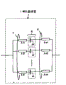
图2示出了根据一种实施方式的功率放大器的第一和第二实例的配置。Fig. 2 shows configurations of first and second examples of a power amplifier according to an embodiment.
图3示出了图2中所示的MOS晶体管的配置图。FIG. 3 shows a configuration diagram of the MOS transistor shown in FIG. 2 .
图4A示出了在栅极长度为90nm的MOS晶体管中,输出功率与负载电阻的相关性。FIG. 4A shows the dependence of output power on load resistance in a MOS transistor with a gate length of 90 nm.
图4B示出了在栅极长度为90nm的MOS晶体管中,寿命与负载电阻的相关性。FIG. 4B shows the dependence of lifetime on load resistance in a MOS transistor with a gate length of 90 nm.
图5A示出了在栅极长度为180nm的MOS晶体管中,输出功率与负载电阻的相关性。FIG. 5A shows the dependence of output power on load resistance in a MOS transistor with a gate length of 180 nm.
图5B示出了在栅极长度为180nm的MOS晶体管中,寿命与负载电阻的相关性。FIG. 5B shows the dependence of lifetime on load resistance in a MOS transistor with a gate length of 180 nm.
图6A示出了在栅极长度为350nm的MOS晶体管中,输出功率与负载电阻的相关性。FIG. 6A shows the dependence of output power on load resistance in a MOS transistor with a gate length of 350 nm.
图6B示出了在栅极长度为350nm的MOS晶体管中,寿命与负载电阻的相关性。FIG. 6B shows the dependence of lifetime on load resistance in a MOS transistor with a gate length of 350 nm.
图7示出了在用于该实施例的功率放大器的第一实例中的栅极长度为90nm的MOS晶体管中,当纵坐标和横坐标分别表示归一化的电压以及负载电阻时,输出功率(实线)和寿命(虚线)的等高线。Fig. 7 shows that in the MOS transistor whose gate length is 90nm in the first example of the power amplifier used in this embodiment, when the ordinate and the abscissa respectively represent the normalized voltage and the load resistance, the output power (solid line) and lifetime (dashed line) contours.
图8A示出在用于该实施例的功率放大器的第二实例中的栅极长度为90nm的MOS晶体管中,输出功率与负载电抗的相关性。FIG. 8A shows the dependence of output power on load reactance in a MOS transistor having a gate length of 90 nm in the second example of the power amplifier used in this embodiment.
图8B示出在用于该实施例的功率放大器的第二实例中的栅极长度为90nm的MOS晶体管中,寿命与负载电抗的相关性。FIG. 8B shows the dependence of lifetime on load reactance in a MOS transistor having a gate length of 90 nm in the second example of the power amplifier used in this embodiment.
图9示出了该实施例的功率放大器的第三实例的配置。FIG. 9 shows the configuration of a third example of the power amplifier of this embodiment.
图10示出了在该实施例的功率放大器的第三实例中使用栅极长度为90nm的MOS晶体管时,输出功率、增益、功率负载效率与输入功率的相关性。FIG. 10 shows the dependence of output power, gain, power load efficiency and input power when a MOS transistor with a gate length of 90 nm is used in the third example of the power amplifier of this embodiment.
图11是描述该实施例的功率放大器的第三实例的控制方法的流程图。FIG. 11 is a flowchart describing a control method of the third example of the power amplifier of this embodiment.
图12示出了该实施例的功率放大器的第四实例的配置。FIG. 12 shows the configuration of a fourth example of the power amplifier of this embodiment.
图13是描述该实施例的功率放大器的第四实例的控制方法的流程图。FIG. 13 is a flowchart describing a control method of the fourth example of the power amplifier of this embodiment.
图14是描述设计该实施例的功率放大器的方法的第一实例的流程图。FIG. 14 is a flowchart describing a first example of a method of designing the power amplifier of this embodiment.
图15是描述设计该实施例的功率放大器的方法的第二实例的流程图。FIG. 15 is a flowchart describing a second example of the method of designing the power amplifier of this embodiment.
图16示出了对于图14中的MOS晶体管作为计算结果的示例性显示而显示的电流-电压特性以及负载圆(load circle)。FIG. 16 shows current-voltage characteristics and load circles displayed for the MOS transistor in FIG. 14 as an exemplary display of calculation results.
图17是对于图15的MOS晶体管作为计算结果的示例性显示而显示的在Smith图上绘制输出电压和寿命的等高线的图。FIG. 17 is a graph plotting contour lines of output voltage and lifetime on a Smith chart displayed as an exemplary display of calculation results for the MOS transistor of FIG. 15 .
具体实施方式 Detailed ways
在下文中,将参照附图描述用于执行本发明的最佳方式。Hereinafter, the best mode for carrying out the invention will be described with reference to the accompanying drawings.
[功率放大器的配置][Configuration of power amplifier]
(第一实例)(first instance)
将描述根据一个实施例的功率放大器的第一实例。A first example of a power amplifier according to an embodiment will be described.
图2示出了根据该实施例的功率放大器的第一实例的配置。具体地,图2示出了在功率放大器是单级放大器时的配置,或者在功率放大器是多级放大器时一级的配置。FIG. 2 shows the configuration of a first example of the power amplifier according to this embodiment. Specifically, FIG. 2 shows a configuration when the power amplifier is a single-stage amplifier, or a configuration of one stage when the power amplifier is a multi-stage amplifier.
参照图2,该实例的功率放大器采用MOS晶体管1作为有源元件。Referring to FIG. 2, the power amplifier of this example employs a
来自输入端子2的信号通过输入匹配电路4输入到MOS晶体管1的栅极端子。通过MOS晶体管1的漏极端子和输出匹配电路5,从输出端子3输出一个输出信号。A signal from the
ZL(=RL+j·XL)限定了利用MOS晶体管的栅极宽度W(mm)归一化的、在从MOS晶体管1的漏极端子看输出匹配电路5时的负载阻抗。ZL (=RL+j·XL) defines the load impedance normalized by the gate width W (mm) of the MOS transistor when the
适当的电位(偏置)从未示出的偏置电路分别施加到MOS晶体管1的栅极端子和漏极端子。Appropriate potentials (biases) are applied to the gate terminal and the drain terminal of the
图3示出了MOS晶体管1的单元配置。FIG. 3 shows the cell configuration of the
参照图3,MOS晶体管1分成多个晶体管单元6,每个晶体管单元包括漏极电极、源极电极和栅极电极(栅指状物)。Referring to FIG. 3 , the
在超高频工作中,从每个晶体管单元6至多根线7,8与之连接的连接点的距离(即多根线7,8的长度)是重要的。在多根线7,8的电长度(electric length)分别是功率放大器的工作频率处十分之一波长或更小时,可以实现有利的功率组合。在这种情形下,前述的ZL可以限定为在输出侧从线8的连接点看时输出匹配电路5的负载阻抗。In UHF operation the distance from each
图4A和4B分别示出了对于栅极长度为90nm的nMOS晶体管所计算的输出功率与负载电阻(RL)的相关性和寿命与RL的相关性,该nMOS晶体管在CMOS工艺中形成。4A and 4B show the calculated output power vs. load resistance (RL) dependence and lifetime vs. RL, respectively, for an nMOS transistor with a gate length of 90 nm formed in a CMOS process.
在这方面,在图4A和4B中,寿命定义为直到将要计算的MOS晶体管中一半的漏极电流减小10%时的时间。此外,对于计算,选择输出功率饱和之前的水平作为输入功率,并且通过栅极宽度归一化的负载电抗(XL)设置为0。此外,归一化的电压Vd_n表示为参数。Vd_n是施加在MOS晶体管1的漏极和源极之间的电压,并且通过DC状态允许的电源电压的最大值Vddmax(在DC状态中允许的值,或者在RF非输入状态中限定的值)归一化。例如,在90nm技术中,1V或1.2V通常用作Vddmax。In this regard, in FIGS. 4A and 4B , the lifetime is defined as the time until the drain current of half of the MOS transistors to be calculated is reduced by 10%. Also, for calculations, the level before output power saturation was chosen as the input power, and the load reactance (XL) normalized by the gate width was set to zero. Furthermore, the normalized voltage Vd_n is expressed as a parameter. Vd_n is a voltage applied between the drain and source of the
参照图4A,输出功率不取决于Vd_n,并且RL达到接近1.3Ω·mm的最大值(峰值)。在每个Vd_n上输出功率达到峰值的位置连接RL的线表示为线A1-A1’。此外,输出功率明显取决于RL的值,并且优选的RL的范围很窄。Referring to FIG. 4A , the output power does not depend on Vd_n, and RL reaches a maximum value (peak value) close to 1.3Ω·mm. The line connecting RL at the point where the output power peaks at each Vd_n is denoted as line A1-A1'. Furthermore, the output power depends significantly on the value of RL, and the range of preferred RL is narrow.
此外,参照图4B,与图4A中的线A1-A1’相对应的连接每个Vd_n上的RL的线表示为线B1-B1’。尽管寿命在Vd_n从0.7至0.9的范围内表现出对RL的很大相关性,对于半导体器件还是保证了1x10⁶-1x10⁸小时的足够的寿命。In addition, referring to FIG. 4B, a line connecting RL on each Vd_n corresponding to the line A1-A1' in FIG. 4A is represented as a line B1-B1'. Although the lifetime shows a large dependence on RL in the range of Vd_n from 0.7 to 0.9, a sufficient lifetime of 1×10 6 -1×10 8 hours is guaranteed for semiconductor devices.
此外,图5A和5B分别示出了对于栅极长度为180nm的nMOS晶体管所计算的寿命与输出功率和RF的相关性,该nMOS晶体管在CMOS工艺中形成,用于与图4A和4B比较。类似地,图5A也通过线A2-A2’表示在输出电压达到峰值的位置连接RL的线;并且图5B也通过线B2-B2’表示与线A2-A2’相对应的连接RL的线。Furthermore, FIGS. 5A and 5B show the calculated lifetime dependence on output power and RF for an nMOS transistor with a gate length of 180 nm formed in a CMOS process for comparison with FIGS. 4A and 4B , respectively. Similarly, Fig. 5A also represents the line connecting RL at the position where the output voltage reaches the peak value by line A2-A2'; and Fig. 5B also represents the line connecting RL corresponding to line A2-A2' by line B2-B2'.
此外,图6A和6B分别示出了对于栅极长度为350nm的nMOS晶体管所计算的寿命与输出功率和RL的相关性,该nMOS晶体管在CMOS工艺中形成,用于与图4A和4B比较。类似地,图6A也通过线A3-A3’表示在输出电压达到峰值的位置连接RL的线;并且图6B也通过线B3-B3’表示与线A3-A3’相对应的连接RL的线。Furthermore, FIGS. 6A and 6B show the calculated lifetime dependence on output power and RL for an nMOS transistor with a gate length of 350 nm formed in a CMOS process for comparison with FIGS. 4A and 4B , respectively. Similarly, Fig. 6A also represents the line connecting RL at the position where the output voltage reaches the peak value by line A3-A3'; and Fig. 6B also represents the line connecting RL corresponding to line A3-A3' by line B3-B3'.
参照图4B、5B和6B,随着RL增加,寿命退化,并且在任何曲线图中,在超过某一RL时退化的比例变得更慢。为了在寿命与RL的相关性波动时定义RL,在每一个曲线图中外推出在低RL区大致描绘曲线的直线,在高RL区大致描绘曲线的直线,以找到两条直线的相交点(P1,P2,P3)。例如,与点Vd_n=0.7相比,P1位于栅极长度为90nm时线B1-B1’的右侧;P2位于栅极长度为180nm时线B2-B2’附近;P3位于栅极长度为350nm时线B3-B3′的左侧。Referring to Figures 4B, 5B and 6B, as RL increases, the lifetime degrades, and in any of the graphs, the proportion of degradation becomes slower beyond a certain RL. To define RL as the lifetime-RL correlation fluctuates, a straight line roughly delineating the curve in the low RL region and a straight line roughly delineating the curve in the high RL region is extrapolated in each graph to find the point of intersection of the two lines (P1 , P2, P3). For example, compared with the point Vd_n=0.7, P1 is located on the right side of the line B1-B1' when the gate length is 90nm; P2 is located near the line B2-B2' when the gate length is 180nm; P3 is located when the gate length is 350nm To the left of line B3-B3'.
具体地,应当理解,对于如图4B所示的栅极长度为90nm的小型栅极,寿命表现出与RL的强相关性,因为P1位于可以产生峰值输出功率处的线B1-B1’的右侧。因而,在这种情形下,应当考虑RL和寿命二者。Specifically, it should be understood that for a small gate with a gate length of 90 nm as shown in Figure 4B, the lifetime exhibits a strong correlation with RL, since P1 is located to the right of the line B1-B1' where peak output power can be generated side. Thus, in this case, both RL and lifetime should be considered.
此外,在栅极长度是图6B所示的350nm的长栅极时,P3位于线B3-B3’的左侧,由此可以理解寿命不是与RL强相关。因而,在这种情形下,取决于Vd_n(电源电压)而不是取决于RL,粗略地确定寿命。In addition, when the gate length is a long gate of 350nm as shown in Fig. 6B, P3 is located on the left side of the line B3-B3', so it can be understood that the lifetime is not strongly correlated with RL. Thus, in this case, the lifetime is roughly determined depending on Vd_n (power supply voltage) instead of depending on RL.
另一方面,当栅极长度为图5B所示的180nm时,P2位于线B2-B2’附近。从该事实可以理解,寿命与RL的相关性波动的边界粗略地位于180nm的栅极长度处。On the other hand, when the gate length is 180 nm as shown in Fig. 5B, P2 is located near the line B2-B2'. It can be understood from this fact that the boundary of the lifetime-RL correlation fluctuation is roughly located at the gate length of 180 nm.
基于该知识,从输出功率和寿命的方面看,Vd_n和RL可以限于优选的范围。Based on this knowledge, Vd_n and RL can be limited to preferred ranges in terms of output power and lifetime.
图7示出了输出功率(相对值,实线)的等高线和寿命的等高线(虚线),横坐标表示归一化的电压Vd_n,纵坐标表示MOS晶体管中的负载电阻。在这种情形下,MOS晶体管1具有90nm的栅极长度。FIG. 7 shows contour lines of output power (relative value, solid line) and lifetime (dotted line), the abscissa represents the normalized voltage Vd_n, and the ordinate represents the load resistance in the MOS transistor. In this case,
此处,基于图7,Vd_n和RL可以限于其中输出功率高并且可以保证足够长的寿命的范围。Here, based on FIG. 7 , Vd_n and RL can be limited to a range in which the output power is high and a sufficiently long lifetime can be secured.
首先,在Vd_n大约为0.9或更小时,保证1x10⁶小时或更长的足够寿命。随后,引用图4B,应当理解,如果Vd_n减小则寿命提高,但如果Vd_n等于或小于0.5则寿命没有提高且输出功率单调减小。因而,Vd_n限于0.5至0.9之间的范围,因为在该范围内最佳。First, a sufficient lifetime of 1x10 6 hours or more is guaranteed when Vd_n is approximately 0.9 or less. Subsequently, referring to FIG. 4B , it should be understood that the lifetime increases if Vd_n decreases, but does not increase and the output power monotonically decreases if Vd_n is equal to or less than 0.5. Therefore, Vd_n is limited to a range between 0.5 and 0.9 because it is optimal within this range.
RL又限于粗略地由RL>0.64×Vd_n+0.19(Ω·mm)和RL<0.64×Vd_ n+1.73(Ω·mm)表示的范围。RL is again limited to ranges roughly represented by RL>0.64×Vd_n+0.19 (Ω·mm) and RL<0.64×Vd_n+1.73 (Ω·mm).
在按照这种方式限制Vd_n和RL的范围中(由图7中的平行四边形表示的范围,下文称为“限制范围”),与寿命的等高线相比,输出功率的等高线延伸到左下。这表示即使采用相同的寿命也可以提供更高的输出功率。In the range where Vd_n and RL are limited in this way (the range indicated by the parallelogram in Fig. 7, hereinafter referred to as the "limited range"), the contour of the output power extends to lower left. This means that higher output power can be provided even with the same lifetime.
例如,在观看图7中寿命为1×10⁸小时的点线时,在限制范围内输出功率(相对值)通常大于10dB,而即使在相同的寿命位于限制范围外部时输出功率也减小。该行为对应于图4A和4B分别示出的输出功率以及寿命与RL的相关性。For example, when looking at the dotted line in Fig. 7 with a lifetime of 1 × 10⁸ hours, the output power (relative value) is usually greater than 10 dB within the limit range, while the output power decreases even when the same lifetime is outside the limit range. This behavior corresponds to the output power and lifetime dependence on RL shown in Figures 4A and 4B, respectively.
综上所述,已经发现,在具有小型栅极的MOS晶体管1中,在其中输出功率高的RL范围内,寿命表现出与RL的强相关性,寿命与RL的相关性波动的边界粗略地位于180nm的栅极长度处,并且如果RL限制在适当的Vd_n以下,可以利用与RL的相关性提供高输出功率和足够长的寿命。In summary, it has been found that, in the
因而,在该实例的功率放大器中,输出匹配电路5设计成提供落在图7中的限制范围内的Vd_n和RL。Thus, in the power amplifier of this example, the
此外,在该实例的功率放大器中,负载阻抗(ZL)的限定是重要的。如上所述,在图3中线8的电长度粗略地为十分之一波长或更小时,可以在线8的连接点处定义用于观看负载阻抗的参考点。另一方面,在线8的电长度大于十分之一波长时,将从每个晶体管单元6看输出侧上的负载阻抗视为ZL是适当的(实际上,ZL/W作为匹配电路的阻抗给出)。此外,如果在从晶体管单元6至线8的连接点的任何位置插入任何元件,则将在从参考点观看输出侧时位于元件前面的负载阻抗(更紧邻晶体管单元6)视为ZL是适当的。Furthermore, in the power amplifier of this example, the definition of the load impedance (ZL) is important. As described above, when the electrical length of the
随后,示出了计算寿命的示例性方法。使用DC状态的寿命τ0,以及测量寿命T0时的Isub_0、Id-0,通过等式(5)计算年龄。Subsequently, an exemplary method of calculating lifetime is shown. Using the lifetime τ 0 in the DC state, and I sub — 0 , I d-0 when the lifetime T 0 was measured, the age is calculated by equation (5).
[等式5][equation 5]
在高频工作时给出相同的Age,等式(1)等于等式(5),使得包括RF状态下的寿命τ的等式由以下的等式(6)给出:Given the same Age when operating at high frequency, Equation (1) is equal to Equation (5), so that the equation including the lifetime τ in the RF state is given by Equation (6) below:
[等式6][equation 6]
假定频率f处的CW(连续波),等式(6)转换为以下的等式(7):Assuming a CW (continuous wave) at frequency f, equation (6) transforms into equation (7) below:
[等式7][equation 7]
此外,τ由以下的等式(8)表示:In addition, τ is represented by the following equation (8):
[等式8][Equation 8]
此处,如果等式(9)中所示的条件成立,τ可以简化地由等式(10)表示:Here, τ can be simplified by Equation (10) if the condition shown in Equation (9) holds:
[等式9][equation 9]
[等式10][equation 10]
前述的等式简单地用在寿命计算的实例中,并且可以更改或改变。The foregoing equations are used simply in the example of life calculation and may be modified or changed.
在如上所述的该实例的功率放大器中,在其中采用栅极长度为180nm或更小的MOS晶体管1的功率放大器中,通过设置Vd_n为0.5-0.9,以及通过设置RL为RL>0.64×Vd_n+0.19(Ω·mm)且RL<0.64×Vd_n+1.73(Ω·mm),可以同时实现高输出功率和长寿命二者。In the power amplifier of this example as described above, in the power amplifier in which the
此外,在该实例的功率放大器配置成具有多级的放大器,可以将其或者串联或者并联组合。Furthermore, the power amplifier in this example is configured as having multiple stages of amplifiers, which can be combined either in series or in parallel.
此外,该实例的功率放大器对于MOS晶体管1优选地采用能够高速工作的n沟道MOS(nMOS)。Furthermore, the power amplifier of this example preferably employs an n-channel MOS (nMOS) capable of high-speed operation for the
此外,在采用栅极长度为180nm或更小的MOS晶体管1时,该实例的功率放大器特别有效,不可以在MOS晶体管1上应用多氧化物技术,其中,优选的可应用频率处于10GHz或更高的微波范围或30GHz或更高的毫米波范围。Furthermore, the power amplifier of this example is particularly effective when using a
(第二实例)(second instance)
将描述根据该实施例的功率放大器的第二实例。应当注意,该实例的功率放大器在自身的配置方面类似于图2所示的第一实例。A second example of the power amplifier according to this embodiment will be described. It should be noted that the power amplifier of this example is similar to the first example shown in FIG. 2 in its own configuration.
该实例的功率放大器除了按照与第一实例类似的方式限制Vd_n和RL之外,还限制了负载电抗(XL)。The power amplifier of this example also limits the load reactance (XL) in addition to limiting Vd_n and RL in a similar manner to the first example.
图8A和8B示出了对于在CMOS工艺中形成的MOS晶体管1所计算的输出功率与XL的相关性和寿命与XL的相关性。在这种情形下,MOS晶体管1具有90nm的栅极长度,并且RL为1.6(Ω·mm)。8A and 8B show the dependence of the output power on XL and the dependence of the lifetime on XL calculated for the
参照图8A和8B,在XL基本上接近零时输出功率变得更大,而寿命也变得更长。此外明显地,寿命具有与XL的强相关性,并且粗略地在XL>-1.28(Ω·mm)和XL<2.05(Ω·mm)的范围内寿命表现出理想值。因而,XL限制在该范围内。Referring to FIGS. 8A and 8B , when XL is substantially close to zero, the output power becomes larger and the lifetime becomes longer. It is also apparent that the lifetime has a strong correlation with XL, and roughly in the range of XL>−1.28 (Ω·mm) and XL<2.05 (Ω·mm), the lifetime exhibits ideal values. Thus, XL is limited to this range.
结果,在该实例的功率放大器中,输出匹配电路5设计成除了第一实例的条件之外,在前述的范围内给出XL。As a result, in the power amplifier of this example, the
(第三实例)(third instance)
将描述根据该实施例的功率放大器的第三实例。A third example of the power amplifier according to this embodiment will be described.
图9示出了该实施例的功率放大器的第三实例的配置。具体地,图9示出了在功率放大器为单级放大器时的配置和在功率放大器为多级放大器时一级的配置。FIG. 9 shows the configuration of a third example of the power amplifier of this embodiment. Specifically, FIG. 9 shows a configuration when the power amplifier is a single-stage amplifier and a configuration of one stage when the power amplifier is a multi-stage amplifier.
参照图9,该实例的功率放大器采用MOS晶体管1作为有源元件。Referring to FIG. 9, the power amplifier of this example employs a
从输入端子2施加的信号通过输入匹配电路4施加到MOS晶体管1的栅极端子。从输出端子3通过输出匹配电路5从MOS晶体管1的漏极端子输出一个输出信号。A signal applied from the
ZL(=RL+j·XL)限定了与利用MOS晶体管的栅极宽度W(mm)归一化的、在从MOS晶体管1的漏极端子看输出匹配电路5时的负载阻抗相等的值。ZL (=RL+j·XL) defines a value equal to the load impedance normalized by the gate width W (mm) of the
此外,MOS晶体管1具有分别与栅极电源电路9和漏极电源电路10相连的栅极端子和漏极端子,从外部进行控制。Furthermore, the
至少漏极电源电路10及其他可以响应来自外部的电源电压指征而改变施加在漏极和源极之间的电压。At least the drain
然后,对于单载波调制(ASK(幅移键控)、FSK(频移键控)、BPSK、QPSK、八相PSK、16QAM),通过将利用DC状态可允许的电压值归一化的电压Vd_n设置为0.5-0.9,并且通过施加相同的电压作为漏源电压,同时实现了可靠性和高输出特性。Then, for single carrier modulation (ASK (Amplitude Shift Keying), FSK (Frequency Shift Keying), BPSK, QPSK, Eight Phase PSK, 16QAM), by normalizing the voltage Vd_n It is set to 0.5-0.9, and by applying the same voltage as the drain-source voltage, both reliability and high output characteristics are achieved.
另一方面,对于多载波调制,Vd_n设置为0.9-1并且作为漏源电压而施加,从而实现了高线性(更高的饱和输出),以同时实现低失真特性和高输出特性。结果,在每种调制方案中可以执行最佳的操作,并且也可以实现更高的效率。On the other hand, for multi-carrier modulation, Vd_n is set to 0.9-1 and applied as a drain-source voltage, thereby achieving high linearity (higher saturated output) to simultaneously realize low distortion characteristics and high output characteristics. As a result, optimal operation can be performed in each modulation scheme, and higher efficiency can also be achieved.
在下文中,将详细描述该实施例的功率放大器的工作。Hereinafter, the operation of the power amplifier of this embodiment will be described in detail.
如上所述,已经发现,在具有小型栅极的MOS晶体管1中,在其中输出功率高的RL范围内,寿命表现出与RL的强相关性,寿命与RL的相关性波动的边界粗略地位于180nm的栅极长度处,并且如果RL限制在适当的Vd_n以下,可以利用与RL的相关性提供高输出功率和足够长的寿命。As described above, it has been found that, in the
换言之,该实例的功率放大器的条件类似于第二实例,其中MOS晶体管1施加有电压Vd_n作为漏源电压,其中利用DC状态可允许的电压值归一化Vd_n,并且设置为0.5-0.9。此外,ZL(=RL+j·XL)表示利用MOS晶体管1的栅极宽度W(mm)对从漏极端子看输出匹配电路5时负载阻抗的归一化所获得的值,其中ZL的实部(RL)是RL>0.64×Vd_n+0.19(Ω·mm)且RL<0.64×Vd_n+1.73(Ω·mm)。进而,ZL的虚部(XL)为XL>-1.28(Ω·mm)且XL<2.05(Ω·mm)。In other words, the condition of the power amplifier of this example is similar to that of the second example in which the
该条件基于向功率放大器施加经过FSK、BPSK、QPSK等作为等幅调制的单载波调制信号的假定,并且基于在输出功率饱和之前输入功率的水平方面所获得的知识。This condition is based on the assumption that a single-carrier modulation signal subjected to FSK, BPSK, QPSK, etc. is applied to the power amplifier as a constant amplitude modulation, and is based on knowledge obtained on the level of input power before the output power is saturated.
另一方面,对于经过OFDM作为二次调制的多载波调制信号,在峰值功率和平均功率之间存在着大的差别,并且在平均功率方面看,工作水平(operation level)变低。例如,功率放大器经常可以在比饱和输出水平低10dB或更多的工作水平下工作。在这种情形下,由于平均输出功率降低,即使作为MOSFET的源漏电压而施加的Vd_n设置为0.9-1.0,在可靠性方面也不会出现问题。On the other hand, for a multicarrier modulated signal subjected to OFDM as secondary modulation, there is a large difference between peak power and average power, and the operation level becomes low in terms of average power. For example, power amplifiers can often operate at
图10示出了在采用栅极长度为90nm的MOS晶体管1的功率放大器(按照三级配置的CMOS放大器,用于60GHz波段)中,输出功率、增益和功率负载效率与输入功率的相关性。FIG. 10 shows the dependence of output power, gain, and power load efficiency on input power in a power amplifier (CMOS amplifier in a three-stage configuration for 60 GHz band) using a
在单载波调制(QPSK)中,在Vd_n设置为0.7(Vd=0.7V)时,可以在1dB增益的压缩点(compressed point)(P1dB)处实现6dBm的输出功率和3%的功率负载效率(PAE)。在其中保证可靠性的条件下,该输出功率最大化。In single carrier modulation (QPSK), when Vd_n is set to 0.7 (Vd=0.7V), an output power of 6dBm and a power load efficiency of 3% can be achieved at the compressed point (P1dB) of 1dB gain ( PAE). This output power is maximized under conditions in which reliability is ensured.
另一方面,在多载波调制中,如果要求为了获得低失真工作而在比P1dB低10dB的点(10dB BO)处工作,在Vd_n=0.7(Vd=0.7V)时所产生的输出功率为-5dBm,并且在Vd_n=1(Vd=1V)时为0dBm,通过提高电压明显改善了输出功率。此外,功率负载效率从小于1%提高至大约1%。在这种情形下,因为输出功率小于单载波调制中的输出功率,在可靠性方面将不会出现问题。On the other hand, in multi-carrier modulation, if it is required to operate at a point 10dB lower than P1dB (10dB BO) in order to obtain low distortion operation, the output power generated at Vd_n=0.7 (Vd=0.7V) is - 5dBm, and 0dBm when Vd_n=1 (Vd=1V), the output power is obviously improved by increasing the voltage. In addition, the power load efficiency is improved from less than 1% to about 1%. In this case, since the output power is smaller than that in single carrier modulation, there will be no problem in terms of reliability.
图11示出了用于描述控制该实例的功率放大器的方法的流程图。具体地,图11示出了通过包括该实例的功率放大器的无线装置执行的控制方法。FIG. 11 shows a flowchart for describing a method of controlling the power amplifier of this example. Specifically, FIG. 11 shows a control method performed by a wireless device including the power amplifier of this example.
参照图11,在开始对功率放大器的控制(S11)时,基于设置来设定调制方案(S12),并且确定施加到功率放大器的信号是否是多载波调制信号(S13)。在施加多载波调制信号时,Vd_n例如设置为1(S14-1)。另一方面,在施加单载波调制信号时,Vd_n例如设置为0.7(S14-2)。随后,指示漏极电源电路10输出该数值的Vd_n(S 15),并且向MOS晶体管1施加来自漏极电源电路10的Vd_n(S16)。因而,结束对功率放大器的控制(S18),随后开始无线通信。通过这些操作,如前所述设置了最佳的电压。Referring to FIG. 11 , upon starting control of the power amplifier (S11), a modulation scheme is set based on settings (S12), and it is determined whether a signal applied to the power amplifier is a multi-carrier modulation signal (S13). When a multi-carrier modulation signal is applied, Vd_n is set to 1, for example (S14-1). On the other hand, when a single carrier modulation signal is applied, Vd_n is set to 0.7, for example (S14-2). Subsequently, the drain
根据如上所述的该实例的功率放大器,通过与两种调制方案(即单载波调制和多载波调制)相对应地控制MOS晶体管1的漏源电压,可以在相应的调制方案中实现高性能。According to the power amplifier of this example as described above, by controlling the drain-source voltage of
(第四实例)(fourth example)
将描述根据该实施例的功率放大器的第四实例。A fourth example of the power amplifier according to this embodiment will be described.
图12示出了该实施例的功率放大器的第四实例的配置。具体地,图12示出了在功率放大器为单级放大器时的配置和在功率放大器为多级放大器时一级的配置。FIG. 12 shows the configuration of a fourth example of the power amplifier of this embodiment. Specifically, FIG. 12 shows a configuration when the power amplifier is a single-stage amplifier and a configuration of one stage when the power amplifier is a multi-stage amplifier.
参照图12,为该实例的功率放大器提供两个功率放大器单元13a,13b。Referring to FIG. 12, two power amplifier units 13a, 13b are provided for the power amplifier of this example.
在功率放大器单元13a,13b中,分别采用MOS晶体管1a,1b作为有源元件。In the power amplifier units 13a, 13b, MOS transistors 1a, 1b are employed as active elements, respectively.
通过从外部进行控制的开关11,向功率放大器单元13a,13b之一施加来自输入端子2的信号。The signal from the
通过输入匹配电路4a,将施加给功率放大器单元13a的信号施加至MOS晶体管1a的栅极端子,并且通过输出匹配电路5a从MOS晶体管1a的漏极端子输出。The signal applied to the power amplifier unit 13a is applied to the gate terminal of the MOS transistor 1a through the
另一方面,通过输入匹配电路4b,将施加给功率放大器单元13b的信号施加至MOS晶体管1b的栅极端子,并且通过输出匹配电路5b从MOS晶体管1b的漏极端子输出。On the other hand, the signal applied to the power amplifier unit 13b is applied to the gate terminal of the MOS transistor 1b through the
通过开关12切换来自每一个功率放大器单元13a,13b的信号输出,类似地从外部进行控制,并且从输出端子3输出。The signal output from each power amplifier unit 13 a , 13 b is switched by the
此外,MOS晶体管1a,1b具有分别与栅极电源电路9和漏极电源电路10相连的栅极端子和漏极端子,从外部进行控制。Furthermore, the MOS transistors 1a and 1b have a gate terminal and a drain terminal respectively connected to a gate
至少漏极电源电路10及其他可以响应来自外部的电源电压指征而改变施加在漏极和源极之间的电压。At least the drain
可以对该实例的功率放大器进行外部控制,以选择功率放大器单元,以及设置所选择的功率放大器单元内的MOS晶体管上所施加的漏源电压。The power amplifier of this example can be controlled externally to select a power amplifier cell and to set the drain-source voltage applied to the MOS transistors in the selected power amplifier cell.
该实例的功率放大器基于与第三实例相同的概念,但在以下的方面有区别。The power amplifier of this example is based on the same concept as the third example, but differs in the following respects.
具体地,与第三实例的功率放大器相比较,该实例的功率放大器包括施加不同电压的多个功率放大器单元,其中至少一个功率放大器单元是施加单载波调制信号的单载波功率放大器单元,并且与此不同的至少一个功率放大器单元是施加多载波调制信号的多载波功率放大器单元。然后,基于向功率放大器施加多载波调制信号还是单载波调制信号,选择和切换单载波功率放大器单元和多载波功率放大器单元。Specifically, compared with the power amplifier of the third example, the power amplifier of this example includes a plurality of power amplifier units applying different voltages, wherein at least one power amplifier unit is a single-carrier power amplifier unit applying a single-carrier modulation signal, and with The different at least one power amplifier unit is a multicarrier power amplifier unit applying a multicarrier modulation signal. Then, the single-carrier power amplifier unit and the multi-carrier power amplifier unit are selected and switched based on whether the multi-carrier modulation signal or the single-carrier modulation signal is applied to the power amplifier.
图13示出了用于描述控制该实例的功率放大器的方法的流程图。具体地,图13示出了通过包括该实例的功率放大器的无线装置执行的控制方法。此外,假定在下文中,功率放大器单元13a是多载波功率放大器单元,且功率放大器单元13b是单载波功率放大器单元。FIG. 13 shows a flowchart for describing a method of controlling the power amplifier of this example. Specifically, FIG. 13 shows a control method performed by a wireless device including the power amplifier of this example. Furthermore, it is assumed that hereinafter, the power amplifier unit 13a is a multi-carrier power amplifier unit, and the power amplifier unit 13b is a single-carrier power amplifier unit.
参照图13,在开始对功率放大器的控制(S11)时,设定调制方案(S12),并且基于设定来确定施加到功率放大器的信号是否是多载波调制信号(S13)。在施加多载波调制信号时,Vd_n例如设置为1(S14-1),指示漏极电源电路10向多载波功率放大器单元13a输出该数值的Vd_n(S15-1),从漏极电源电路10向功率放大器单元13a内的MOS晶体管1a施加Vd n(S16-1),并且切换开关11,12以选择多载波功率放大器单元13a(S17-1)。因而,结束对功率放大器的控制(S18),随后开始无线通信。另一方面,在施加单载波调制信号时,Vd_n例如设置为0.7(S14-2),指示漏极电源电路10向单载波功率放大器单元13b输出该数值的Vd_n(S15-2),从漏极电源电路10向功率放大器单元13b内的MOS晶体管1b施加Vd_n(S16-2),并且切换开关11,12以选择单载波功率放大器单元13b(S17-2)。因而,结束对功率放大器的控制(S18),随后开始无线通信。Referring to FIG. 13 , when the control of the power amplifier is started (S11), a modulation scheme is set (S12), and based on the setting, it is determined whether a signal applied to the power amplifier is a multi-carrier modulation signal (S13). When a multi-carrier modulation signal is applied, Vd_n is set to 1 (S14-1), for example, and the drain
根据如上所述的该实例的功率放大器,通过与两种调制方案(即单载波调制和多载波调制)相关联地切换和使用其漏源电压不同、分别包括MOS晶体管1a,1b的功率放大器单元13a,13b,可以在相应的调制方案中实现高性能。According to the power amplifier of this example as described above, by switching and using power amplifier units whose drain-source voltages are different, including MOS transistors 1a, 1b respectively, in association with two modulation schemes, namely, single-carrier modulation and multi-carrier modulation 13a, 13b, can achieve high performance in corresponding modulation schemes.
在这方面,尽管在第三和第四实例中对于Vd_n使用了特定的值,但Vd_n对于单载波调制可以设置为0.5至0.9,对于多载波调制可以设置为比单载波调制更大的数值。此外,考虑到通常电源电压的精度等,Vd_n对于多载波调制优选地在0.9至1之间,其中考虑了10%的波动。In this regard, although a specific value is used for Vd_n in the third and fourth examples, Vd_n can be set to 0.5 to 0.9 for single carrier modulation and to a larger value than for single carrier modulation for multicarrier modulation. In addition, Vd_n is preferably between 0.9 and 1 for multi-carrier modulation, taking into account the 10% fluctuation, in consideration of the accuracy of the usual power supply voltage and the like.
此外,尽管第三和第四实例已经示出了示例性的控制方法,本发明不限于前述的控制方法,只要Vd_n可以改变或者功率放大器单元可以根据调制方案切换即可。Furthermore, although the third and fourth examples have shown exemplary control methods, the present invention is not limited to the aforementioned control methods as long as Vd_n can be changed or the power amplifier unit can be switched according to the modulation scheme.
[设计功率放大器的方法][How to Design a Power Amplifier]
(第一实例)(first instance)
将描述测量根据该实施例的功率放大器的第一示例性方法。A first exemplary method of measuring the power amplifier according to this embodiment will be described.
图14示出了用于描述设计该实施例的功率放大器的第一示例性方法(部分)的流程图。具体地,图14示出了通过由计算机执行的支持软件(设计CAD工具等)执行的设计图2中所示的功率放大器的方法。Fig. 14 shows a flowchart for describing a first exemplary method (part) of designing the power amplifier of this embodiment. Specifically, FIG. 14 shows a method of designing the power amplifier shown in FIG. 2 performed by supporting software (design CAD tool, etc.) executed by a computer.
参照图14,在开始设计功率放大器(S1)时,对模拟器设置MOS晶体管1的偏置条件(S2),并且设置输入功率(S3)。随后,对模拟器设置负载阻抗(ZL)(S4)。随后,指示模拟器,例如利用等式(8)或等式(9)的右侧的数值计算MOS晶体管1的寿命(S5-1)。确定对于所有的预定负载阻抗是否已经完成计算(S6),如果未完成,重复步骤S4,S5-1,并且在改变负载阻抗的设置的同时计算寿命。在完成计算时,指示模拟器显示计算结果(S7),并且基于该计算结果设计输出匹配电路5(S8)。因而,结束功率放大器的设计(S9)。Referring to FIG. 14, when starting to design the power amplifier (S1), the bias condition of the
(第二实例)(second instance)
将描述设计该实施例的功率放大器的第二示例性方法。A second exemplary method of designing the power amplifier of this embodiment will be described.
在图14中所示的第一实例中,将注意力放在寿命与负载阻抗的相关性上来设计功率放大器,然而,也可以组合另外的性能指数。In the first example shown in Fig. 14, the power amplifier is designed focusing on the dependence of the lifetime on the load impedance, however, other performance indices can also be combined.
例如,在功率放大器中,输出功率、功率增益和效率取决于负载阻抗,存在着用于澄清这些相关性的称为“负载拉升”(load pull)的FET评估方法。并且,通常,在设计功率放大器的模拟器上表现出称为“负载拉升”的该FET评估方法。For example, in power amplifiers, output power, power gain, and efficiency depend on load impedance, and there is a FET evaluation method called "load pull" to clarify these dependencies. And, usually, this FET evaluation method called "load pull" is performed on a simulator for designing power amplifiers.
图15示出了表示设计该实施例的功率放大器的第二示例性方法(部分)的流程图。具体地,图15示出了通过由计算机执行的支持软件(设计CAD工具等)执行的设计图2中所示的功率放大器的方法。Fig. 15 shows a flowchart representing a second exemplary method (part) of designing the power amplifier of this embodiment. Specifically, FIG. 15 shows a method of designing the power amplifier shown in FIG. 2 performed by supporting software (design CAD tool, etc.) executed by a computer.
参照图15,设计该实施例的功率放大器的方法是其将负载拉升与寿命计算相结合的方法,并且,具体地在图15中,将注意力放在输出功率及负载拉升。Referring to FIG. 15 , the method of designing the power amplifier of this embodiment is its method of combining load pull with lifetime calculation, and, specifically in FIG. 15 , attention is paid to output power and load pull.
该实例的设计功率放大器的方法不同于第一实例之处仅在于:对于MOS晶体管1,除了计算寿命(S5-1)之外,还计算输出功率(S5-2)。The method of designing a power amplifier of this example differs from the first example only in that, for the
在下文中,将参照图16和17描述在图14和15中所示的S7处对MOS晶体管1的计算结果的示例性显示,Hereinafter, an exemplary display of the calculation result for the
图16示出了MOS晶体管1的电流-电压特性,作为在图14中所示的S7处对MOS晶体管1的计算结果的示例性显示。通过设置偏置点和负载阻抗,可以利用模拟器绘制图16类似的负载圆。尽管在图16中也绘制了归一化的衬底电流(Isub)的等高线,然而可以例如使用等式(7)-(9)计算等高线。FIG. 16 shows the current-voltage characteristics of the
同时,也绘出了负载圆(例如,在功率放大器的工作频率为60GHz时)。在该情形下,通过在时间上累积沿负载圆俘获的Isub、漏极电流等,计算由等式(1)表示的Age,并且Age的倒数是寿命。图16的绘图对于作为保证寿命的参考是有用的。At the same time, a load circle is also drawn (for example, when the operating frequency of the power amplifier is 60 GHz). In this case, Age expressed by Equation (1) is calculated by temporally accumulating Isub captured along the load circle, drain current, etc., and the reciprocal of Age is the lifetime. The plot of Figure 16 is useful as a reference for guaranteed life.
图17是在表示负载阻抗的Smith图上绘出输出功率和寿命的等高线的图,作为图14中所示的S7处对MOS晶体管的计算结果的示例性显示而示出。利用图17,一下子就可以理解是否可以实现所需的输出功率和寿命。因而,图17对于显示计算结果(S7)是很有用的。此外,在针对每一个电源电压(或归一化的电压)来绘制图17时,可以容易地理解输出功率、寿命以及电源电压之间的关系,因而在设计时提供了不可限量的优点。FIG. 17 is a graph plotting contour lines of output power and lifetime on a Smith chart representing load impedance, shown as an exemplary display of calculation results for MOS transistors at S7 shown in FIG. 14 . Using Fig. 17, it is possible to understand at a glance whether the desired output power and lifetime can be achieved. Thus, Fig. 17 is useful for displaying the calculation result (S7). Furthermore, when graph 17 is plotted for each supply voltage (or normalized voltage), the relationship between output power, lifetime, and supply voltage can be easily understood, thus providing unlimited advantages in design.
顺便指出,图16的绘图给出了一些额外的知识。例如,在负载阻抗的虚部(负载电抗XL)取很大的正值或负值时,负载圆膨胀,甚至进入其中衬底电流指数增加的右侧(朝向更高的电压)。可以估计,这导致寿命退化,并且是在该实施例的功率放大器的第二实例中将假想值限制在零附近的基础。此外,在功率放大器采用诸如GaAs的化合物半导体的情形下,通常不在高频下绘制图16所示的狭窄负载圆。据推测,这主要归因于寄生电抗分量。Incidentally, the plot of Figure 16 gives some additional insight. For example, when the imaginary part of the load impedance (load reactance XL) takes large positive or negative values, the load circle expands even into the right side (towards higher voltages) where the substrate current increases exponentially. It can be estimated that this leads to lifetime degradation, and is the basis for limiting the phantom value to around zero in the second example of the power amplifier of this embodiment. Also, in the case of a power amplifier employing a compound semiconductor such as GaAs, the narrow load circle shown in FIG. 16 is generally not drawn at high frequencies. Presumably, this is mainly due to the parasitic reactance component.
由于该实施例的功率放大器采用MOS晶体管形成工艺(包括CMOS工艺),其中涉及短栅极长度和精细布线规则,可以理解,即使在等于或高于10GHz的高频下,也存在着一些寄生电抗分量,在其中XL很小的区域可以实现狭窄的负载圆,并且限制了寿命的退化。从利用这方面进行验证的事实来讲,图16在设计期间是有效的。Since the power amplifier of this embodiment employs MOS transistor formation processes (including CMOS processes), which involve short gate lengths and fine wiring rules, it can be understood that there are some parasitic reactances even at high frequencies equal to or higher than 10 GHz component, a narrow load circle can be achieved in the area where the XL is small, and life degradation is limited. Figure 16 is valid during design in terms of the fact that it is verified using this aspect.
如上所述,根据设计功率放大器的第一和第二示例性方法,可能有利地澄清MOS晶体管1的输出功率和寿命之间的关系,并且因为OS晶体管1的性能容易得知,可能在短时间内设计高性能功率放大器。此外,有利地,可以在考虑MOS晶体管1的寿命、增益、效率、失真特性等的同时设计出功率放大器。As described above, according to the first and second exemplary methods of designing a power amplifier, it is possible to advantageously clarify the relationship between the output power and the lifetime of the
尽管已经参照实施例描述了本发明,但本发明不限于实施例。在本发明的范围内,可以按照不同的方式对本发明在配置和细节上进行更改,这些方式是本领域的技术人员可以理解的。Although the present invention has been described with reference to the embodiments, the present invention is not limited to the embodiments. The present invention may be modified in configuration and details in various ways within the scope of the present invention, which will be understood by those skilled in the art.
本申请要求基于2007年10月31日提交的JP-2007-283539和2008年5月20日提交的JP-2008-131772的优先权,其公开内容以全文引用的方式包含在本文中。This application claims priority based on JP-2007-283539 filed on October 31, 2007 and JP-2008-131772 filed on May 20, 2008, the disclosures of which are incorporated herein by reference in their entirety.
Claims (8)
Applications Claiming Priority (5)
| Application Number | Priority Date | Filing Date | Title |
|---|---|---|---|
| JP2007-283539 | 2007-10-31 | ||
| JP2007283539 | 2007-10-31 | ||
| JP2008131772 | 2008-05-20 | ||
| JP2008-131772 | 2008-05-20 | ||
| PCT/JP2008/066095 WO2009057385A1 (en) | 2007-10-31 | 2008-09-05 | Power amplifier and power amplifier control method |
Publications (2)
| Publication Number | Publication Date |
|---|---|
| CN101842978A CN101842978A (en) | 2010-09-22 |
| CN101842978B true CN101842978B (en) | 2014-03-12 |
Family
ID=40590786
Family Applications (1)
| Application Number | Title | Priority Date | Filing Date |
|---|---|---|---|
| CN200880113793.0A Expired - Fee Related CN101842978B (en) | 2007-10-31 | 2008-09-05 | Power amplifier and power amplifier control method |
Country Status (5)
| Country | Link |
|---|---|
| US (1) | US8326244B2 (en) |
| JP (1) | JP5141690B2 (en) |
| CN (1) | CN101842978B (en) |
| TW (1) | TWI397256B (en) |
| WO (1) | WO2009057385A1 (en) |
Families Citing this family (6)
| Publication number | Priority date | Publication date | Assignee | Title |
|---|---|---|---|---|
| EP2346175B1 (en) * | 2010-01-15 | 2015-03-11 | Telefonaktiebolaget L M Ericsson | A method and apparatuses for transmitter to multi-carrier power amplifier configuration |
| JP5720927B2 (en) * | 2010-10-25 | 2015-05-20 | ソニー株式会社 | Receiving device and method, demodulating device and method, and program |
| JP5896718B2 (en) * | 2011-02-04 | 2016-03-30 | 日本電波工業株式会社 | Piezoelectric oscillator |
| US8779868B2 (en) | 2011-03-10 | 2014-07-15 | Harris Corporation | Mobile wireless communications device with adjustable impedance matching network and associated methods |
| JP5829957B2 (en) | 2012-03-16 | 2015-12-09 | パナソニック株式会社 | Wireless communication device |
| JP6430122B2 (en) * | 2014-02-06 | 2018-11-28 | 株式会社東芝 | amplifier |
Citations (4)
| Publication number | Priority date | Publication date | Assignee | Title |
|---|---|---|---|---|
| EP1096670A2 (en) * | 1999-10-08 | 2001-05-02 | M/A-Com Eurotec | System and method for transmitting digital information using interleaved delta modulation |
| JP2001257544A (en) * | 2000-03-13 | 2001-09-21 | Hitachi Kokusai Electric Inc | MOS-FET amplifier circuit |
| CN1636315A (en) * | 2002-02-21 | 2005-07-06 | 艾利森公司 | Current modulator with dynamic amplifier impedance compensation |
| US20050200407A1 (en) * | 2001-12-12 | 2005-09-15 | Renesas Technology Corp. | High frequency power amplifier and wireless communication module |
Family Cites Families (9)
| Publication number | Priority date | Publication date | Assignee | Title |
|---|---|---|---|---|
| JP2540928B2 (en) * | 1988-12-21 | 1996-10-09 | 日本電気株式会社 | Logic circuit |
| JPH09330344A (en) | 1996-06-10 | 1997-12-22 | Mitsubishi Electric Corp | Semiconductor device design support apparatus and design support method |
| JP2000174559A (en) | 1998-12-03 | 2000-06-23 | Mitsubishi Electric Corp | Microwave power amplifier |
| JP2000323709A (en) | 1999-03-09 | 2000-11-24 | Fujitsu Ltd | Hot carrier deterioration simulation method, semiconductor device manufacturing method, and computer-readable recording medium |
| US6813319B1 (en) * | 1999-10-08 | 2004-11-02 | M/A-Com Eurotec | System and method for transmitting digital information using interleaved delta modulation |
| JP4095753B2 (en) | 2000-03-30 | 2008-06-04 | 株式会社ルネサステクノロジ | Computer-readable storage medium and semiconductor device design method |
| JP2003298364A (en) | 2002-04-03 | 2003-10-17 | Hitachi Ltd | High frequency power amplifier |
| JP4255703B2 (en) | 2003-01-29 | 2009-04-15 | 三菱電機株式会社 | Cascode power amplifier |
| JP2005259777A (en) | 2004-03-09 | 2005-09-22 | Matsushita Electric Ind Co Ltd | Reliability simulation method for semiconductor device |
-
2008
- 2008-09-05 CN CN200880113793.0A patent/CN101842978B/en not_active Expired - Fee Related
- 2008-09-05 WO PCT/JP2008/066095 patent/WO2009057385A1/en not_active Ceased
- 2008-09-05 US US12/682,175 patent/US8326244B2/en not_active Expired - Fee Related
- 2008-09-05 JP JP2009538976A patent/JP5141690B2/en not_active Expired - Fee Related
- 2008-10-22 TW TW097140444A patent/TWI397256B/en not_active IP Right Cessation
Patent Citations (4)
| Publication number | Priority date | Publication date | Assignee | Title |
|---|---|---|---|---|
| EP1096670A2 (en) * | 1999-10-08 | 2001-05-02 | M/A-Com Eurotec | System and method for transmitting digital information using interleaved delta modulation |
| JP2001257544A (en) * | 2000-03-13 | 2001-09-21 | Hitachi Kokusai Electric Inc | MOS-FET amplifier circuit |
| US20050200407A1 (en) * | 2001-12-12 | 2005-09-15 | Renesas Technology Corp. | High frequency power amplifier and wireless communication module |
| CN1636315A (en) * | 2002-02-21 | 2005-07-06 | 艾利森公司 | Current modulator with dynamic amplifier impedance compensation |
Non-Patent Citations (1)
| Title |
|---|
| JP特开平2001-257544A 2001.09.21 |
Also Published As
| Publication number | Publication date |
|---|---|
| US8326244B2 (en) | 2012-12-04 |
| US20100225399A1 (en) | 2010-09-09 |
| CN101842978A (en) | 2010-09-22 |
| TW200937846A (en) | 2009-09-01 |
| JP5141690B2 (en) | 2013-02-13 |
| WO2009057385A1 (en) | 2009-05-07 |
| JPWO2009057385A1 (en) | 2011-03-10 |
| TWI397256B (en) | 2013-05-21 |
Similar Documents
| Publication | Publication Date | Title |
|---|---|---|
| Voinigescu et al. | Silicon millimeter-wave, terahertz, and high-speed fiber-optic device and benchmark circuit scaling through the 2030 ITRS horizon | |
| Srivastava et al. | MOSFET technologies for double-pole four-throw radio-frequency switch | |
| TWI675551B (en) | Body-biased switching device | |
| US7619482B1 (en) | Compact low voltage low noise amplifier | |
| Srivastava et al. | Design and performance analysis of double-gate MOSFET over single-gate MOSFET for RF switch | |
| CN101842978B (en) | Power amplifier and power amplifier control method | |
| CN103516342B (en) | Body contact portion depleted silicon on insulator transistor | |
| US20010040479A1 (en) | Electronic switch | |
| JP6616949B2 (en) | Low noise amplifier drain switch circuit | |
| KR20010070295A (en) | High frequency power amplifier module and wireless communication system | |
| CN107924938A (en) | High Performance RF Switches | |
| Callender et al. | FinFET for mm wave-technology and circuit design challenges | |
| Nakatani et al. | Millimeter-wave GaN power amplifier MMICs for 5G application | |
| US6734509B2 (en) | Semiconductor integrated circuit | |
| US20110294444A1 (en) | Switching device, radio frequency signal switch, and radio frequency signal amplification module | |
| Engelmann et al. | A broadband 22nm FDSOI D-band power amplifier with dynamic back gate bias gain-linearization achieving 9.6% PAE at 8.7 dBm OPldB and 3.7% at 6 dB back-off | |
| Jain et al. | Novel mmWave NMOS device for high pout mmWave power amplifiers in 45RFSOI | |
| US20110025579A1 (en) | Semiconductor device, and radio frequency switch and radio frequency module using the semiconductor device | |
| Rusanen et al. | Ka-band stacked power amplifier on 22 nm CMOS FDSOI technology utilizing back-gate bias for linearity improvement | |
| Gu et al. | Low insertion loss and high linearity PHEMT SPDT and SP3T switch ICs for WLAN 802.11 a/b/g applications | |
| JP5450955B2 (en) | High frequency switch | |
| CN102549916B (en) | Dual use transistor | |
| US11368127B2 (en) | Active mixer and method for improving gain and noise | |
| Laha et al. | 60 GHz OOK transmitter in 32 nm DG FinFET technology | |
| Gangadharan et al. | Comparator Based Envelope Tracking for RF PA Using FinFET |
Legal Events
| Date | Code | Title | Description |
|---|---|---|---|
| C06 | Publication | ||
| PB01 | Publication | ||
| C10 | Entry into substantive examination | ||
| SE01 | Entry into force of request for substantive examination | ||
| GR01 | Patent grant | ||
| GR01 | Patent grant | ||
| CF01 | Termination of patent right due to non-payment of annual fee | ||
| CF01 | Termination of patent right due to non-payment of annual fee |
Granted publication date: 20140312 |