CN101840968A - A semiconductor optoelectronic element capable of improving light extraction rate and its manufacturing method - Google Patents
A semiconductor optoelectronic element capable of improving light extraction rate and its manufacturing method Download PDFInfo
- Publication number
- CN101840968A CN101840968A CN200910119566A CN200910119566A CN101840968A CN 101840968 A CN101840968 A CN 101840968A CN 200910119566 A CN200910119566 A CN 200910119566A CN 200910119566 A CN200910119566 A CN 200910119566A CN 101840968 A CN101840968 A CN 101840968A
- Authority
- CN
- China
- Prior art keywords
- light
- layer
- light emitting
- substrate
- type
- Prior art date
- Legal status (The legal status is an assumption and is not a legal conclusion. Google has not performed a legal analysis and makes no representation as to the accuracy of the status listed.)
- Granted
Links
Images


Landscapes
- Led Devices (AREA)
Abstract
Description
技术领域technical field
本发明涉及一种半导体光电元件的结构及其制造方法,特别涉及包含突出结构的半导体光电元件的结构及其制造方法。The invention relates to a structure of a semiconductor optoelectronic element and a manufacturing method thereof, in particular to a structure of a semiconductor optoelectronic element including a protruding structure and a manufacturing method thereof.
背景技术Background technique
发光二极管(Light Emitting Diode;简称LED),为一种可将电能转化为光能的电子元件,并同时具备二极管的特性。一般给予直流电时,发光二极管会稳定地发光,但如果接上交流电,发光二极管会呈现闪烁的形态,闪烁的频率依据输入交流电的频率而定。发光二极管的发光原理是外加电压使得电子与空穴在半导体内结合后,将能量以光的形式释放。Light Emitting Diode (LED for short) is an electronic component that can convert electrical energy into light energy, and also has the characteristics of a diode. Generally, when DC power is supplied, the LEDs will emit light steadily, but if AC power is connected, the LEDs will flash, and the frequency of the flashing depends on the frequency of the input AC power. The light-emitting principle of a light-emitting diode is that an external voltage causes electrons and holes to combine in a semiconductor, and release energy in the form of light.
对于发光二极管而言,寿命长、低发热量及低耗电量,并且可以节约能源及减少污染是最大的优点。发光二极管的应用面很广,然而发光效率为其中一个有待提升的问题,也始终困扰着发光二极管照明技术的推广普及。发光效率要提升,有效增加取出效率就是其中一个方法。For light-emitting diodes, long life, low calorific value, low power consumption, energy saving and pollution reduction are the biggest advantages. Light-emitting diodes have a wide range of applications, but luminous efficiency is one of the problems that needs to be improved, and it has always plagued the promotion and popularization of light-emitting diode lighting technology. To improve the luminous efficiency, effectively increasing the extraction efficiency is one of the methods.
传统的发光二极管结构受限于全反射及横向波导效应,无法将发光层所产生的光全部取出,使得发光二极管整体的取光率偏低。The traditional light-emitting diode structure is limited by total reflection and transverse waveguide effect, and cannot extract all the light generated by the light-emitting layer, so that the overall light extraction rate of the light-emitting diode is low.
以氮化镓系(GaN)三族氮化物发光二极管为例,氮化镓(GaN)的折射率为2.5,空气折射率为1,假定光的射出是在均匀的光学表面,可以计算出来全反射的临界角为23.5度。当光从氮化镓系(GaN)发光二极管发光层射出,只要入射角度大于23.5度,就会全部反射回材料内部。目前发展出许多技术试着有效提升光的取出效率,而表面微结构工艺是提高发光二极管出光效率的其中一个有效技术。一种方法为中国台湾专利公开号码I296861,即于发光区域外围的n型披覆层形成一粗糙表面,降低产生全反射的情形。Taking the gallium nitride (GaN) group III nitride light-emitting diode as an example, the refractive index of gallium nitride (GaN) is 2.5, and the refractive index of air is 1. Assuming that the light is emitted on a uniform optical surface, the full The critical angle for reflection is 23.5 degrees. When the light is emitted from the light-emitting layer of the gallium nitride (GaN) light-emitting diode, as long as the incident angle is greater than 23.5 degrees, it will all be reflected back into the material. At present, many technologies have been developed to try to effectively improve the light extraction efficiency, and the surface microstructure process is one of the effective technologies to improve the light extraction efficiency of LEDs. One method is Taiwan Patent Publication No. I296861, that is, the n-type cladding layer on the periphery of the light-emitting region forms a rough surface to reduce the occurrence of total reflection.
另外,中国台湾专利公开号码200701521、美国专利公告号码US6953952B2、美国专利公告号码US 7358544B2以及美国专利公开号码US2007/0228393的发明所述,该发明于发光区域外围形成多个柱状结构并围绕于所述的发光区域,其柱状结构的高度与发光区域的高度可以相等,柱状的角度范围约30~80度,以降低全反射的现象。请参考图1,显示一现有技术俯视图,为半导体光电元件为同面电极形式的俯视图。在图1中,发光区域110上形成一p型电极114,发光区域旁边形成一n型电极115。多个柱状结构122位于元件切割平台124上,围绕于所述发光区域110与所述n型电极115周围。所述多个柱状结构122之间包含多个隙缝123。由于光无方向性以及光子的位置分布在发光层的每一点,其结构可以使得大部分光线利用柱状结构的角度及高度改变光线折射角度而射出,但是光子也可能遇到柱状结构之间的缝隙而无法射出,仍然在发光区域的结构内全反射或是折射,最后转换成热能。In addition, as described in the inventions of Taiwan Patent Publication No. 200701521, U.S. Patent Publication No. US6953952B2, U.S. Patent Publication No. US 7358544B2 and U.S. Patent Publication No. US2007/0228393, the invention forms a plurality of columnar structures on the periphery of the light-emitting area and surrounds the described In the light-emitting area, the height of the columnar structure can be equal to the height of the light-emitting area, and the angle range of the columnar structure is about 30-80 degrees, so as to reduce the phenomenon of total reflection. Please refer to FIG. 1 , which shows a top view of a prior art, which is a top view of a semiconductor optoelectronic element in the form of electrodes on the same plane. In FIG. 1 , a p-
发明内容Contents of the invention
鉴于上述的发明背景中,为了符合产业利益的需求,改善上述的问题,以及提高半导体光电元件的光转换率,本发明提供一种半导体光电元件,主要于发光区域外围以至少一个突出结构围绕。In view of the above-mentioned background of the invention, in order to meet the needs of industrial interests, improve the above-mentioned problems, and improve the light conversion rate of the semiconductor optoelectronic element, the present invention provides a semiconductor optoelectronic element, which is mainly surrounded by at least one protruding structure around the periphery of the light-emitting area.
本发明提供一种能够提升光取出率的半导体光电元件的结构,包含一基板,一发光区域,至少一个突出结构,其中的突出结构位于一元件切割平台上并与所述发光区域间隔一沟槽,以及围绕于所述发光区域周围,所述发光区域包含一n型导通层位于该基板上,一发光层位于该n型导通层上,一p型导通层位于该发光层上。The invention provides a structure of a semiconductor optoelectronic element capable of improving the light extraction rate, comprising a substrate, a light-emitting area, and at least one protruding structure, wherein the protruding structure is located on an element cutting platform and separated from the light-emitting area by a groove , and surrounding the light-emitting area, the light-emitting area includes an n-type conduction layer on the substrate, a light-emitting layer on the n-type conduction layer, and a p-type conduction layer on the light-emitting layer.
所述基板与所述n型导通层之间可包含一缓冲层,所述发光层与所述p型导通层之间可包含一电子阻挡层,一透明导电层位于所述发光区域上,一n型电极位于n型导通层上,一p型电极位于所述透明导电层上,最后一保护层覆盖于所述发光区域并暴露出该p型电极,或是覆盖于所述发光区域及所述突出结构并暴露出所述p型电极及n型电极。A buffer layer may be included between the substrate and the n-type conduction layer, an electron blocking layer may be included between the light-emitting layer and the p-type conduction layer, and a transparent conductive layer is located on the light-emitting region , an n-type electrode is located on the n-type conduction layer, a p-type electrode is located on the transparent conductive layer, and the last protective layer covers the light-emitting region and exposes the p-type electrode, or covers the light-emitting region and the protruding structure and expose the p-type electrode and n-type electrode.
所述突出结构与所述发光区域之间间隔一沟槽,所述沟槽的宽度介于0.1至10μm之间。A groove is spaced between the protruding structure and the light emitting region, and the width of the groove is between 0.1 μm and 10 μm.
所述突出结构的侧面为一倾斜面,该倾斜面的切面可为梯形或是三角形。The side of the protruding structure is an inclined surface, and the cut surface of the inclined surface can be trapezoidal or triangular.
所述倾斜面的倾斜角度范围介于45°~90°之间。The range of inclination angle of the inclined surface is between 45° and 90°.
所述倾倾斜角度范围介于65°~80°之间。The range of the inclination angle is between 65° and 80°.
所述突出结构的高度介于p型导通层及n型导通层之间,其宽度介于0.1至10μm之间。The height of the protruding structure is between the p-type conduction layer and the n-type conduction layer, and its width is between 0.1 and 10 μm.
另外,本发明也提供一种能够提升光取出率的半导体光电元件的制造方法,包含提供一基板,形成一发光结构于所述基板上,蚀刻所述发光结构以形成一发光区域、一元件切割平台以及一突出结构位于所述元件切割平台上,所述突出结构与所述发光区域之间间隔一沟槽并围绕于所述发光区域。In addition, the present invention also provides a method for manufacturing a semiconductor optoelectronic element capable of improving the light extraction rate, including providing a substrate, forming a light-emitting structure on the substrate, etching the light-emitting structure to form a light-emitting region, cutting the element The platform and a protruding structure are located on the component cutting platform, and a groove is spaced between the protruding structure and the light emitting area and surrounds the light emitting area.
所述基板与所述n型导通层之间可包含形成一层缓冲层,所述发光层与所述p型导通层之间可包含形成一层电子阻挡层,一透明导电层形成于所述发光区域上。一n型电极形成于n型欧姆接触层上,一p型电极形成于所述透明导电层上。最后一保护层覆盖于所述发光区域并暴露出该p型电极,或是覆盖于所述发光区域及所述突出结构并暴露出所述p型电极及n型电极。A buffer layer may be formed between the substrate and the n-type conduction layer, an electron blocking layer may be formed between the light-emitting layer and the p-type conduction layer, and a transparent conduction layer is formed on on the light-emitting area. An n-type electrode is formed on the n-type ohmic contact layer, and a p-type electrode is formed on the transparent conductive layer. The last protection layer covers the light-emitting region and exposes the p-type electrode, or covers the light-emitting region and the protruding structure and exposes the p-type electrode and the n-type electrode.
上述的结构可让光线除了直接由p型导通层的方向向外射出,也可从内部经由反射或折射后而自突出结构向外射出。所述突出结构以围绕方式位于发光区域周围可增加光线经过的可能性,进而减少内部能量的损耗,有效提高光取出率效益。The above-mentioned structure allows light not only to be emitted outward directly from the direction of the p-type conduction layer, but also to be emitted outward from the protruding structure after being reflected or refracted from inside. The protruding structure is located around the light-emitting area in a surrounding manner to increase the possibility of light passing through, thereby reducing the loss of internal energy and effectively improving the efficiency of light extraction.
附图说明Description of drawings
图1为本发明的现有技术;Fig. 1 is the prior art of the present invention;
图2为本发明单一突出结构的同面电极形式半导体光电元件俯视图;Fig. 2 is the top view of the same-plane electrode form semiconductor optoelectronic element with single protruding structure of the present invention;
图3(a)至图3(g)为图2A到A′的截面的各步骤结构形成示意图;Fig. 3 (a) to Fig. 3 (g) is each step structure formation schematic diagram of the section of Fig. 2A to A';
图4为本发明多个突出结构的同面电极形式半导体光电元件俯视图;Fig. 4 is a top view of a semiconductor optoelectronic element in the form of a plurality of protruding structures in the same plane of the present invention;
图5为图4B到B′的截面的示意图;Fig. 5 is the schematic diagram of the section of Fig. 4B to B';
图6(a)为本发明突出结构放大图;Fig. 6 (a) is the enlarged view of the protruding structure of the present invention;
图6(b)为本发明突出结构示意图;Figure 6(b) is a schematic diagram of the prominent structure of the present invention;
图7为本发明单一突出结构的双面电极形式半导体光电元件俯视图;7 is a top view of a semiconductor photoelectric element in the form of double-sided electrodes with a single protrusion structure of the present invention;
图8为图7C到C′的截面的示意图;Figure 8 is a schematic view of the cross-section of Figure 7C to C';
图9为本发明多个突出结构的双面电极形式半导体光电元件俯视图;Fig. 9 is a top view of a semiconductor optoelectronic element in the form of double-sided electrodes with multiple protruding structures in the present invention;
图10为图9D到D′的截面的示意图;Fig. 10 is a schematic diagram of the cross section of Fig. 9D to D';
图11(a)至图11(e)为多个突出结构的分离式同面电极形式半导体光电元件各步骤结构形成示意图;Figure 11(a) to Figure 11(e) are schematic diagrams of the formation of the structure of each step of the semiconductor optoelectronic element in the form of separate electrodes with multiple protruding structures;
图12为本发明与现有技术单独的半导体光电元件结构的发光光场图;Fig. 12 is the luminous light field diagram of the semiconductor optoelectronic element structure of the present invention and the prior art alone;
图13为本发明的突出结构中倾斜角度及围绕在发光区域数目与光增益的关系图。FIG. 13 is a graph showing the relationship between the inclination angle and the number of surrounding light-emitting regions and light gain in the protruding structure of the present invention.
上述附图中的附图标记说明如下:The reference numerals in the above-mentioned accompanying drawings are explained as follows:
101 基板 102 缓冲层101
103 GaN层 104 n型导通层103 GaN layer 104 n-type conduction layer
105 发光层 106 电子阻挡层105
107 p型导通层 109 发光结构107 p-
110 发光区域 101 基板110
111 111a 111b 111c 突出结构111
112 透明导电层112 transparent conductive layer
113 113a 113b 113c 沟槽113
114 p型电极 115 n型电极114 p-type electrode 115 n-type electrode
116 保护层 117 沟槽的宽度116
118 突出结构高度 119 突出结构宽度118
120 倾斜角度A120 Tilt angle A
121 导电材料层 122 柱状结构121
123 隙缝 124 元件切割平台123
125 突出结构切面 126 突出结构表面125 Protruding Structural Sections 126 Protruding Structural Surfaces
127 金属层 128 第一表面127
129 第二表面129 second surface
具体实施方式Detailed ways
本发明在此所探讨的方向为一种能够提升光取出率的半导体光电元件及其制造方法。为了能彻底地了解本发明,将在下列的描述中提出详尽的步骤及其组成。显然地,本发明的实施并未限定于半导体光电元件工艺的领域普通技术人员所公知的特殊细节。另一方面,众所周知的组成或步骤并未描述于细节中,以避免造成本发明不必要的限制。本发明的较佳实施例会详细描述如下,然而除了这些详细描述之外,本发明还可以广泛地实施在其他的实施例中,且本发明的范围不受限定,其以之后的权利要求为准。The direction of the present invention discussed here is a semiconductor optoelectronic element capable of improving the light extraction rate and its manufacturing method. In order to provide a thorough understanding of the present invention, detailed steps and components thereof will be set forth in the following description. Obviously, the practice of the invention is not limited to specific details known to those skilled in the art of semiconductor optoelectronic element processing. On the other hand, well-known components or steps have not been described in detail so as not to unnecessarily limit the invention. The preferred embodiments of the present invention will be described in detail as follows, but in addition to these detailed descriptions, the present invention can also be widely implemented in other embodiments, and the scope of the present invention is not limited, it is based on the following claims .
本发明利用半导体光电结构经外延后,通过蚀刻过程形成一突出结构与一发光区域。所述的突出结构及发光区域之间间隔一沟槽,且所述的突出结构围绕于该发光区域周围。因为光线是无方向性的,当发光区域的发光层产生光线后,光线除了从p型导通层方向射出外,同时也会朝内部方向或侧边方向射出。随着光线从内部经由反射或折射后而自突出结构向外射出,除了增加半导体光电元件的亮度以外,并提高半导体光电元件的光取出效益。In the present invention, a protruding structure and a light-emitting area are formed through an etching process after epitaxy of the semiconductor optoelectronic structure. A groove is separated between the protruding structure and the light emitting area, and the protruding structure surrounds the light emitting area. Because the light is non-directional, when the light-emitting layer in the light-emitting region generates light, the light will not only be emitted from the direction of the p-type conduction layer, but also be emitted toward the inner direction or the side direction. As the light is emitted from the protruding structure after being reflected or refracted from the inside, in addition to increasing the brightness of the semiconductor optoelectronic element, it also improves the light extraction efficiency of the semiconductor optoelectronic element.
从本发明的手段中,本发明提供一种能够提升光取出率的半导体光电元件的结构,包含一基板,一发光区域,一突出结构,其中所述突出结构位于一元件切割平台上并与所述发光区域间隔一沟槽,以及围绕于所述发光区域周围。From the means of the present invention, the present invention provides a structure of a semiconductor optoelectronic element capable of improving the light extraction rate, comprising a substrate, a light-emitting region, and a protruding structure, wherein the protruding structure is located on a component cutting platform and is connected to the The light emitting area is separated by a groove and surrounds the light emitting area.
所述发光区域包含一n型导通层位于所述基板上,一发光层位于所述n型导通层上,一p型导通层位于所述发光层上。The light emitting area includes an n-type conduction layer on the substrate, a light-emitting layer on the n-type conduction layer, and a p-type conduction layer on the light-emitting layer.
所述基板与所述n型导通层之间可包含一缓冲层。所述发光层与所述p型导通层之间可包含一电子阻挡层。一透明导电层位于所述发光区域上。一n型电极位于n型导通层上。一p型电极位于所述透明导电层上。最后一保护层覆盖于所述发光区域并暴露出该p型电极,或是覆盖于所述发光区域及所述突出结构并暴露出所述p型电极及n型电极。A buffer layer may be included between the substrate and the n-type conduction layer. An electron blocking layer may be included between the light emitting layer and the p-type conduction layer. A transparent conductive layer is located on the light emitting area. An n-type electrode is located on the n-type conduction layer. A p-type electrode is located on the transparent conductive layer. The last protection layer covers the light-emitting region and exposes the p-type electrode, or covers the light-emitting region and the protruding structure and exposes the p-type electrode and the n-type electrode.
所述基板可为蓝宝石(Al2O3)基板、碳化硅(SiC)基板、铝酸锂基板(LiAlO2)、镓酸锂基板(LiGaO2)、硅(Si)基板、氮化镓(GaN)基板、氧化锌(ZnO)基板、氧化铝锌基板(AlZnO)、砷化镓(GaAs)基板、磷化镓(GaP)基板、锑化镓基板(GaSb)、磷化铟(InP)基板、砷化铟(InAs)基板或硒化锌(ZnSe)基板。The substrate can be sapphire (Al 2 O 3 ) substrate, silicon carbide (SiC) substrate, lithium aluminate substrate (LiAlO 2 ), lithium gallate substrate (LiGaO 2 ), silicon (Si) substrate, gallium nitride (GaN ) substrate, zinc oxide (ZnO) substrate, aluminum zinc oxide substrate (AlZnO), gallium arsenide (GaAs) substrate, gallium phosphide (GaP) substrate, gallium antimonide substrate (GaSb), indium phosphide (InP) substrate, Indium Arsenide (InAs) substrate or Zinc Selenide (ZnSe) substrate.
所述缓冲层可为氮化镓(GaN)、氮化铝镓(AlGaN)、氮化铝(AlN)、或是InxGa1-xN/InyGa1-yN超晶格结构;其中x≠y。The buffer layer can be gallium nitride (GaN), aluminum gallium nitride (AlGaN), aluminum nitride (AlN), or an In x Ga 1-x N/InyGa 1-y N superlattice structure; where x ≠y.
所述n型导通层包含掺质为硅(Si),p型导通层包含掺质为镁(Mg)。The n-type conduction layer contains silicon (Si) dopant, and the p-type conduction layer contains magnesium (Mg) dopant.
所述透明导电层可为镍金合金(Ni/Au)、氧化铟锡(Indium Tin Oxide;ITO)、氧化铟锌(Indium Zinc Oxide;IZO)、氧化铟钨(Indium Tungsten Oxide;IWO)或是氧化铟镓(Indium Gallium Oxide;IGO)。The transparent conductive layer can be nickel-gold alloy (Ni/Au), indium tin oxide (Indium Tin Oxide; ITO), indium zinc oxide (Indium Zinc Oxide; IZO), indium tungsten oxide (Indium Tungsten Oxide; IWO) or Indium Gallium Oxide (IGO).
一n型电极电性连接所述n型导通层,一p型电极电性连接所述p型导通层。An n-type electrode is electrically connected to the n-type conduction layer, and a p-type electrode is electrically connected to the p-type conduction layer.
所述保护层可为二氧化硅(SiO2)或氮化硅(Si3N4)。The protection layer may be silicon dioxide (SiO 2 ) or silicon nitride (Si 3 N 4 ).
所述突出结构与所述发光区域之间间隔一沟槽而且所述多突出结构之间间隔一沟槽,所述沟槽的宽度介于0.1至10μm之间。A groove is spaced between the protruding structure and the light-emitting area, and a groove is spaced between the multi-protruding structures, and the width of the groove is between 0.1 μm and 10 μm.
所述突出结构的侧面为一倾斜面,其倾斜面的倾斜角度范围介于45°~90°之间,其较佳倾斜角度范围范围介于65°~80°之间。其切面可为梯形或是三角形。The side of the protruding structure is an inclined surface, and the inclined angle range of the inclined surface is between 45°-90°, and the preferred range of the inclined angle is between 65°-80°. Its section can be trapezoidal or triangular.
所述突出结构的高度介于p型导通层及n型导通层之间,其宽度介于0.1至10μm之间。The height of the protruding structure is between the p-type conduction layer and the n-type conduction layer, and its width is between 0.1 and 10 μm.
另外,本发明提供能够提升光取出率的半导体光电元件的制造方法。包含提供一基板。形成一发光结构于所述基板上。蚀刻所述发光结构以形成一发光区域、一元件切割平台以及一突出结构位于所述元件切割平台上。所述突出结构与所述发光区域之间间隔一沟槽并围绕于所述发光区域。In addition, the present invention provides a method for manufacturing a semiconductor photoelectric element capable of improving the light extraction rate. Including providing a substrate. A light emitting structure is formed on the substrate. The light emitting structure is etched to form a light emitting area, a device cutting platform and a protruding structure located on the device cutting platform. A groove is spaced between the protruding structure and the light emitting area and surrounds the light emitting area.
所述发光结构包含一n型导通层位于该基板上,一发光层位于该n型导通层上,一p型导通层位于该发光层上。The light-emitting structure includes an n-type conduction layer on the substrate, a light-emitting layer on the n-type conduction layer, and a p-type conduction layer on the light-emitting layer.
所述基板与所述n型导通层之间可包含形成一层缓冲层。所述发光层与所述p型导通层之间可包含一电子阻挡层。一透明导电层形成于所述发光区域上。一n型电极形成于n型导通层上,一p型电极形成于所述透明导电层上。最后一保护层覆盖于所述发光区域并暴露出该p型电极,或是覆盖于所述发光区域及所述突出结构并暴露出所述p型电极及n型电极。A buffer layer may be formed between the substrate and the n-type conduction layer. An electron blocking layer may be included between the light emitting layer and the p-type conduction layer. A transparent conductive layer is formed on the light emitting area. An n-type electrode is formed on the n-type conduction layer, and a p-type electrode is formed on the transparent conduction layer. The last protection layer covers the light-emitting region and exposes the p-type electrode, or covers the light-emitting region and the protruding structure and exposes the p-type electrode and the n-type electrode.
上述的实施内容,将搭配附图与各步骤的结构示意图详细介绍本发明的结构与各步骤的形成方式。In the above implementation content, the structure of the present invention and the formation method of each step will be described in detail in conjunction with the accompanying drawings and the structural schematic diagrams of each step.
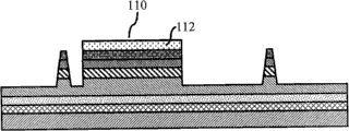
本发明提供一种能够提高光取出率的半导体光电元件的结构。请参考图2,显示本发明单一突出结构的同面电极形式半导体光电元件俯视图。其发光区域110上形成一p型电极114,在所述发光区域110旁边形成一n型电极115。一突出结构111位于元件切割平台124上,与所述发光区域110及所述n型电极115之间间隔一沟槽113,并围绕于所述发光区域110与所述n型电极115周围。接下来,请参考图3(a)至图3(g),为图2A到A′的截面的各步骤结构形成示意图。The present invention provides a structure of a semiconductor photoelectric element capable of improving the light extraction rate. Please refer to FIG. 2 , which shows a top view of a semiconductor optoelectronic device in the form of a same-plane electrode with a single protrusion structure of the present invention. A p-
图3(a)所示,进行基板101表面的净化处理。提供一基板101,例如:蓝宝石(Al2O3)基板、碳化硅(SiC)基板、铝酸锂基板(LiAlO2)、镓酸锂基板(LiGaO2)、硅(Si)基板、氮化镓(GaN)基板、氧化锌(ZnO)基板、氧化铝锌基板(AlZnO)、砷化镓(GaAs)基板、磷化镓(GaP)基板、锑化镓基板(GaSb)、磷化铟(InP)基板、砷化铟(InAs)基板或硒化锌(ZnSe)基板。将基材表面进行清洗。例如:于充满氢气的环境中以1200℃温度进行热清洗(thermal cleaning)。再通入氨气与三族元素的有机金属先驱物(precursor)。可以采用铝、镓或铟的有机金属化合物作为该有机金属先驱物,例如:三甲基铝(trimethylaluminum;TMAl)或是三乙基铝(triethylaluminum;TEAl)、三甲基镓(trimethylgalliaum;TMGa)、三乙基镓(triethylgalliaum;TEGa)、三甲基铟(trimethylindium;TMIn)及三乙基铟(triethylindium;TEIn)等。As shown in FIG. 3( a ), the surface of the
图3(b)所示,于所述基板101上形成一缓冲层102。由于晶格结构与晶格常数是另一项选择外延基板的重要依据。若基板与外延层之间晶格常数差异过大,往往需要先形成一缓冲层才可以得到较佳的外延品质。所述缓冲层102形成的方式是以化学气相沉积法(Chemical Vapor Deposition;CVD)。例如有机金属化学气相沉积(MOCVD;Metal Organic Chemical Vapor Deposition)机台或是分子束外延(MBE;Molecular Beam Epitaxy)机台,以相对于后续正常外延温度较低的环境长晶。例如氮化铝镓铟的一般长晶温度约在800~1400℃之间,而缓冲层的长晶温度约在250~700℃之间。当使用有机金属化学气相沉积法时,氮的先驱物可以是NH3或是N2,镓的先驱物可以是三甲基镓(trimethylgallium;TMGa)或是三乙基镓(triethylgallium;TEGa),铝的先驱物可以是三甲基铝(trimethylaluminum;TMAl)或是三乙基铝(triethylaluminum;TEAl),而铟的先驱物可以是三甲基铟(trimethylindium;TMIn)或是三乙基铟(triethylindium;TEIn)。反应室的压力可以是低压或是常压。缓冲层102可为氮化镓(GaN)、氮化铝镓(AlGaN)、氮化铝(AlN)、或是InxGa1-xN/InyGa1-yN超晶格结构,其中氮化铝(AlN)为TG公司申请的缓冲层专利,氮化铝镓(AlGaN)为日亚化学公司申请的缓冲层专利,而InxGa1-xN/InyGa1-yN超晶格结构为先进开发光电股份有限公司所申请的缓冲层专利。有关于形成InxGa1-xN/InyGa1-yN超晶格结构的技术,可以参阅先进开发光电股份有限公司的专利申请提案,中国台湾专利申请号096104378。As shown in FIG. 3( b ), a
图3(c)所示,完成缓冲层102后,于缓冲层102上外延形成一发光结构109。为提升发光结构的外延晶格的成长品质,可先形成一无掺杂的氮化镓层(GaN)103或是氮化铝镓层(AlGaN)在缓冲层102上。形成一无参杂氮化物层103后,掺杂四族的原子以形成n型导通层104。在本实施例中是硅原子(Si),而硅的先驱物在有机金属化学气相沉积机台中可以是硅甲烷(SiH4)或是硅乙烷(Si2H6)。n型导通层104的形成方式依序由高浓度掺杂硅原子(Si)的氮化镓层(GaN)或是氮化铝镓层(AlGaN)至低浓度掺杂硅原子(Si)的氮化镓层或是氮化铝镓层(AlGaN)。高浓度掺杂硅原子(Si)的氮化镓层(GaN)或是氮化铝镓层(AlGaN)可以提供n型电极之间较佳的导电效果。As shown in FIG. 3( c ), after the
接着是形成一发光层105在n型导通层上。其中发光层105可以是单异质结构、双异质结构、单量子阱层或是多重量子阱层结构。目前多采用多重量子阱层结构,也就是多重量子阱层/阻挡层的结构。量子阱层可以使用氮化铟镓(InGaN),而阻挡层可以使用氮化铝镓(AlGaN)等的三元结构。另外,也可以采用四元结构,也就是使用氮化铝镓铟(AlxInyGa1-x-yN)同时作为量子阱层以及阻挡层。其中调整铝与铟的比例使得氮化铝镓铟晶格的能阶可以分别成为高能阶的阻挡层与低能阶的量子阱层。发光层105可以掺杂n型或是p型的掺杂子(dopant),可以是同时掺杂n型与p型的掺杂子,也可以完全不掺杂。并且,可以是量子阱层掺杂而阻挡层不掺杂、量子阱层不掺杂而阻挡层掺杂、量子阱层与阻挡层都掺杂或是量子阱层与阻挡层都不掺杂。再者,也可以在量子阱层的部分区域进行高浓度的掺杂(delta doping)。Next, a
之后,在发光层105上形成一p型导通的电子阻挡层106。p型导通的电子阻挡层106包括第一种III-V族半导体层,以及第二种III-V族半导体层。这两种III-V族半导体层的能隙不同,且具有周期性地重复沉积在上述发光层105上,前周期性地重复沉积动作可形成能障较高的电子阻挡层(能障高于有源发光层的能障),用以阻挡过多电子(e-)溢流发光层105。所述第一种III-V族半导体层可为氮化铝铟镓(AlxInyGa1-x-yN)层,所述第二种III-V族半导体层可为氮化铝铟镓(AluInvGa1-u-vN)层。其中,0<x≤1,0≤y<1,x+y≤1,0≤u<1,0≤v≤1以及u+v≤1。当x=u时,y≠v。另外,所述III-V族半导体层也可为氮化镓(GaN)、氮化铝(AlN)、氮化铟(InN)、氮化铝镓(AlGaN)、氮化铟镓(InGaN)、氮化铝铟(AlInN)。After that, a p-type conduction
最后,掺杂二族的原子以形成p型导通层107于电子阻挡层106上。在本实施例中是镁原子。而镁的先驱物在有机金属化学气相沉积机台中可以是CP2Mg。p型导通层107的形成方式依序由低浓度掺杂镁原子(Mg)的氮化镓层(GaN)或是氮化铝镓层(AlGaN)至高浓度掺杂镁原子(Mg)的氮化镓层或是氮化铝镓层(AlGaN)。高浓度掺杂镁原子(Mg)的氮化镓层(GaN)或是氮化铝镓层可以提供p型电极之间较佳的导电效果。Finally, group II atoms are doped to form a p-
如图3(d)所示,在完成外延后,通过光致抗蚀剂自旋涂布机以离心力将光致抗蚀剂全面涂布于发光结构109的表面上方以形成光致抗蚀剂膜。再以光刻法(Photolithography)将光致抗蚀剂膜图案化而形成掩模,使得预计蚀刻部分显露。再以电感式等离子体蚀刻系统(Inductively coupled plasma etcher;ICP)蚀刻出发光区域110、突出结构111、元件切割平台124及暴露出n型导通层104,最后再去光致抗蚀剂。所述突出结构111位于所述元件切割平台124上,与所述发光区域110间隔一沟槽113,以及围绕于该发光区域110周围。若为多个突出结构则多个突出结构111之间单独间隔一沟槽113以及平行方式围绕于该发光区域110。As shown in FIG. 3( d), after the epitaxy is completed, the photoresist is fully coated on the surface of the
关于突出结构111的结构特性做进一步说明。请参考图6(a),显示突出结构放大图。所述突出结构111与发光区域110之间以及多个突出结构之间的沟槽宽度117介于0.1至10μm之间。突出结构的宽度119介于0.1至10μm之间。突出结构的高度118介于p型导通层及n型导通层之间。请参考图6(b),显示突出结构示意图所示。突出结构的侧面为一倾斜面,且其倾斜角度为角度“A”120范围介于45°~90°之间,其较佳范围介于65°~80°之间。突出结构切面125为梯形或是三角形。The structural characteristics of the protruding
图3(e)所示,蚀刻出发光区域110及突出结构111后,接着形成一透明导电层112于所述的发光区域110上方。所述透明导电层112必须要有高穿透率和高导电特性,可以透光且使电流均匀分散。一般以蒸镀,溅镀等物理气相沉积法形成透明导电层112于发光区域110上。其材料可为镍金合金(Ni/Au)、氧化铟锡(Indium Tin Oxide;ITO)、氧化铟锌(Indium Zinc Oxide;IZO)、氧化铟钨(Indium Tungsten Oxide;IWO)或是氧化铟镓(Indium Gallium Oxide;IGO)。As shown in FIG. 3( e ), after the
图3(f)所示,形成一p型电极114于透明导电层112上以电性连接p型导通层107,以及形成一n型电极115电性连接于n型导通层104上。所述p型电极114的材料可为镍金合金(Ni/Au)、铂金合金(Pt/Au)、钨(W)、铬金合金(Cr/Au)或钯(Pd)。所述n型电极115的材料可为Ti/Al/Ti/Au(钛/铝/钛/金)、铬金合金(Cr/Au)或Pd/Au(铅/金)。As shown in FIG. 3( f ), a p-
图3(g)所示,最后形成一保护层116。所述保护层116可覆盖于所述发光区域110并暴露出p型电极114、覆盖于该发光区域110及该突出结构111并暴露出该p型电极114,或是覆盖于该发光区域110及该突出结构111并暴露出p型电极114及n型电极115。所述保护层116保护发光区域110不易受到外界污染或干扰而导致受损。所述保护层116的材料可为二氧化硅(SiO2)或氮化硅(Si3N4)。As shown in FIG. 3(g), a
本发明的突出结构可多个平行地围绕于发光区域。请参考图4,显示本发明多个突出结构的同面电极形式半导体光电元件俯视图。其中包含一发光区域110上形成一p型电极114,所述发光区域110旁边形成一n型电极115。多个突出结构111位于n型电极115位于n型导通层104上及所述发光区域110旁边。多个突出结构111a、111b及111c位于元件切割平台124上。所述突出结构111a及所述发光区域110之间间隔一沟槽113a。突出结构之间间隔着多个沟槽113b及113c。其以平行方式围绕着所述发光区域110及所述n型电极115。突出结构的数目并无限定,一保护层116覆盖于所述发光区域110及多个突出结构111a、111b及111c上方,暴露所述p型电极114及n型电极115,或是所述保护层116仅覆盖于所述发光区域110上暴露所述p型电极114。A plurality of protruding structures of the present invention can surround the light emitting area in parallel. Please refer to FIG. 4 , which shows a top view of a semiconductor photoelectric element in the form of same-plane electrodes with multiple protruding structures of the present invention. Therein, a p-
一般商业上以使用蓝宝石(Al2O3)基板为主,但因蓝宝石基板有导电性不佳及不易散热等缺点,可能降低半导体光电元件的信赖度(Reliability)。为减少所述的因素影响半导体光电元件的信赖度,本发明人也采用碳化硅(SiC)基板、硅(Si)基板、氮化镓(GaN)基板、砷化镓(GaAs)基板、磷化镓(GaP)基板、锑化镓基板(GaSb)、磷化铟(InP)基板、砷化铟(InAs)基板或硒化锌(ZnSe)基板等具有导电性以及散热性较佳等特性的基板,形成双面电极形式的半导体光电元件结构。Generally, sapphire (Al 2 O 3 ) substrates are mainly used commercially, but the sapphire substrate has disadvantages such as poor conductivity and difficulty in heat dissipation, which may reduce the reliability of semiconductor optoelectronic devices. In order to reduce the reliability of semiconductor optoelectronic components due to the factors mentioned above, the inventors also use silicon carbide (SiC) substrates, silicon (Si) substrates, gallium nitride (GaN) substrates, gallium arsenide (GaAs) substrates, phosphide Gallium (GaP) substrates, gallium antimonide substrates (GaSb), indium phosphide (InP) substrates, indium arsenide (InAs) substrates, or zinc selenide (ZnSe) substrates and other substrates with good electrical conductivity and heat dissipation , forming a semiconductor photoelectric element structure in the form of double-sided electrodes.
请参考图7,显示本发明单一突出结构的双面电极形式半导体光电元件俯视图。一发光区域110上形成一p型电极114。一突出结构111位于元件切割平台124上,与所述发光区域110之间间隔一沟槽113,并围绕于所述发光区域110周围。接下来,请参考图8,为图7C到C′的截面的示意图。一发光区域110上形成一透明导电层112。一p型电极114位于所述透明导电层112上。一突出结构111位于元件切割平台124上,与所述发光区域110之间间隔一沟槽113,并围绕于所述发光区域110周围。一n型电极115位于基板101下方。Please refer to FIG. 7 , which shows a top view of a semiconductor optoelectronic device in the form of double-sided electrodes with a single protrusion structure of the present invention. A p-
另外,所述双面电极形式半导体光电元件也可为多个突出结构,请参考图9,显示本发明多个突出结构的双面电极形式半导体光电元件俯视图。其中包含一发光区域110上形成一p型电极114。多个突出结构111位于元件切割平台124上。第一突出结构111a与所述发光区域110之间间隔一沟槽113a。所述第一突出结构111a及第二突出结构111b之间间隔一沟槽113b与第二突出结构111b及第三突出结构111c之间间隔一沟槽113c。所述多个突出结构111平行并围绕于所述发光区域110周围。接下来,请参考图10,为图9D到D′的截面的示意图。从本截面图中可以清楚看出一发光区域110上方形成一透明导电层112。一p型电极114位于所述透明导电层112上方。多个突出结构111a、111b及111c位于元件切割平台124上。所述突出结构111a及所述发光区域110之间间隔一沟槽113a,突出结构之间间隔着多个沟槽113b及113c,其以平行方式围绕着所述发光区域110。突出结构的数目并无限定。一保护层116覆盖于所述发光区域110及多个突出结构111a、111b及111c上方,暴露所述p型电极114,或是所述保护层116仅覆盖于所述发光区域110上暴露所述p型电极114。一n型电极位于所述基板101下方。In addition, the double-sided electrode form semiconductor optoelectronic element can also have multiple protruding structures. Please refer to FIG. 9 , which shows a top view of the double-sided electrode form semiconductor optoelectronic element of the present invention with multiple protruding structures. A p-
另外,在半导体的外延制造过程中,由于半导体层与异质基板之间的晶格常数与热膨胀系数的差异,容易造成半导体于外延过程中产生穿透错位与热应力的问题。因此,本发明的另一种制造方法即以半导体分离的技术降低所述的问题,并增加本发明的光电元件的稳定性。In addition, in the semiconductor epitaxial manufacturing process, due to the difference in lattice constant and thermal expansion coefficient between the semiconductor layer and the heterogeneous substrate, it is easy to cause the problems of penetration dislocation and thermal stress in the semiconductor during the epitaxial process. Therefore, another manufacturing method of the present invention is to use semiconductor separation technology to reduce the above problems and increase the stability of the photovoltaic device of the present invention.
下述几种半导体分离的技术为先进开发光电股份有限公司的专利申请提案。先经由基板与发光结构分离后,再以蚀刻工艺形成发光区域与突出结构。(本部分的图示步骤即为图11(a)至图11(e),将由蚀刻步骤开始说明,而半导体分离的技术将不在本说明书赘述)The following semiconductor separation technologies are proposed by Advanced Development Optoelectronics Co., Ltd. for patent applications. After being separated from the light-emitting structure through the substrate, the light-emitting region and the protruding structure are formed by an etching process. (The illustrated steps in this part are Figure 11(a) to Figure 11(e), which will be described starting from the etching step, and the semiconductor separation technology will not be described in this specification)
第一种半导体分离的方法为成长一第一三族氮化合物半导体层于一暂时基板的表面,以光刻蚀刻工艺图案化所述第一三族氮化合物半导体层。形成一第二三族氮化合物半导体层于所述已图案化的第一三族氮化合物半导体层上。形成一导电材料层于所述第二三族氮化合物半导体层,以及自所述第一三族氮化合物半导体层分离以得到第二三族氮化合物半导体层及导电材料层的组合体。关于本第一种半导体分离的步骤的详细的内容与形成方式,可以参阅先进开发光电股份有限公司的专利申请提案,中国台湾专利申请号097107609。The first semiconductor separation method is to grow a first III-group nitrogen compound semiconductor layer on the surface of a temporary substrate, and pattern the first III-group nitrogen compound semiconductor layer by a photolithographic etching process. A second group-III nitride compound semiconductor layer is formed on the patterned first group-III nitride compound semiconductor layer. A conductive material layer is formed on the second Group-III nitride compound semiconductor layer, and separated from the first Group-III nitride compound semiconductor layer to obtain a combination of the second Group-III nitride compound semiconductor layer and the conductive material layer. For the detailed content and formation method of the first semiconductor separation step, please refer to the patent application proposal of Advanced Development Optoelectronics Co., Ltd., China Taiwan Patent Application No. 097107609.
第二种半导体分离的方法为成长一第一三族氮化合物半导体层于一原始基板的表面。形成一外延阻断层于所述第一三族氮化合物半导体层。成长一第二三族氮化合物半导体层于所述外延阻断层及无覆盖的所述第一三族氮化合物半导体层上。移除所述外延阻断层。成长一第三三族氮化合物半导体层于所述第二三族氮化合物半导体层上。沉积一导电材料层于所述第三三族氮化合物半导体层上,以及将所述第三三族氮化合物半导体层及其上结构自所述第二三族氮化合物半导体层分离。关于本第二种半导体分离的方法的详细的内容与形成方式,可以参阅先进开发光电股份有限公司的专利申请提案,中国台湾专利申请号097115512。The second semiconductor separation method is to grow a first group III nitrogen compound semiconductor layer on the surface of an original substrate. An epitaxial blocking layer is formed on the first Group-III nitride compound semiconductor layer. A second group-III nitride compound semiconductor layer is grown on the epitaxial blocking layer and the uncovered first group-III nitride compound semiconductor layer. The epitaxial blocking layer is removed. A third group III nitrogen compound semiconductor layer is grown on the second group III nitrogen compound semiconductor layer. Depositing a conductive material layer on the third group III nitrogen compound semiconductor layer, and separating the third group III nitrogen compound semiconductor layer and its upper structure from the second group III nitrogen compound semiconductor layer. For the detailed content and formation method of the second semiconductor separation method, please refer to the patent application proposal of Advanced Development Optoelectronics Co., Ltd., China Taiwan Patent Application No. 097115512.
第三种半导体分离的方法为首先,配置一掩模于一基板上,并退火此一掩模以形成多个掩模部,再通过多个掩模部间的空隙将基板蚀刻出多个柱体,最后再分离掩模与基板,即可形成一具有柱阵列的基板,其中上述的多个柱体即构成上述的柱阵列。随后通过此一柱阵列进行外延生长一半导体层,并对柱阵列进行湿蚀刻以分离此一半导体层与基板,借此以取得一独立式(free-standing)的块材或薄膜。关于本第三种半导体分离的方法的详细的内容与形成方式,可以参阅先进开发光电股份有限公司的专利申请提案,中国台湾专利申请号097117099。The third semiconductor separation method is firstly to arrange a mask on a substrate, and anneal the mask to form a plurality of mask parts, and then etch the substrate to form a plurality of pillars through the gaps between the plurality of mask parts. body, and finally the mask and the substrate are separated to form a substrate with a pillar array, wherein the above-mentioned plurality of pillars constitute the above-mentioned pillar array. A semiconductor layer is then epitaxially grown through the pillar array, and the pillar array is wet-etched to separate the semiconductor layer from the substrate, thereby obtaining a free-standing bulk or film. For the detailed content and formation method of the third semiconductor separation method, please refer to the patent application proposal of Advanced Development Optoelectronics Co., Ltd., China Taiwan Patent Application No. 097117099.
本发明以第二种半导体分离的方法后续工艺为例继而说明。请参考图11(a)所示,以电镀或复合电镀方式形成于一导电材料层121于所述发光结构109的第一表面128上。所述发光结构109与所述导电材料121之间包含一层金属层127。然后再分离所述基板101与所述发光结构109,使得暴露出相对于所述发光结构109第一表面128的第二表面129。所述导电材料可为铜(Cu)、镍(Ni)或是钨铜合金(CuW)。所述发光结构包含n型导通层104、发光层105、电子阻挡层106、p型导通层107。其中p型导通层107为所述发光结构109的第一表面128,相对于所述发光结构109第一表面的第二表面129为n型导通层104。The present invention is described by taking the subsequent process of the second semiconductor separation method as an example. Please refer to FIG. 11( a ), a
请参考图11(b)所示,通过光致抗蚀剂自旋涂布机以离心力将光致抗蚀剂剂全面涂布于发光结构的表面上方以形成光致抗蚀剂膜。再以光刻法(Photolithography)将光致抗蚀剂膜图案化而形成光掩模,使得预计蚀刻部分显露。再以电感式等离子体蚀刻系统(Inductively coupled plasma etcher;ICP)蚀刻出一发光区域110、多个突出结构111a、111b以及111c、沟槽113a、113b以及113b、一元件切割平台124并暴露出n型导通层104。同时也分隔出每个单位裸片,以利后续的切割。最后再去光致抗蚀剂。所述突出结构111a与所述发光区域110间隔一沟槽113a。突出结构111a、111b以及111c之间间隔着多个沟槽113b及113c,其以平行方式围绕着所述发光区域110,突出结构的数目并无限定。Please refer to FIG. 11( b ), the photoresist is fully coated on the surface of the light-emitting structure by a photoresist spin coater with centrifugal force to form a photoresist film. The photoresist film is then patterned by photolithography to form a photomask, so that the expected etching portion is exposed. Then use an inductively coupled plasma etcher (ICP) to etch a
关于突出结构111的要求仍与所述同面电极形式以及双面电极形式相同。请参考图6(a),显示突出结构放大图。所述突出结构111与发光区域110之间以及多个突出结构之间的沟槽宽度117介于0.1至10μm之间。突出结构的宽度119介于0.1至10μm之间。突出结构的高度118介于p型导通层及n型导通层之间。请参考图6(b),显示突出结构示意图。突出结构的侧面为一倾斜面,且其倾斜角度120范围介于45°~90°之间,其较佳范围介于65°~80°之间。突出结构切面125为梯形或是三角形。The requirements on the protruding
请参考图11(c)所示,蚀刻完成后,接着形成一透明导电层112于所述的发光区域110上方。所述透明导电层112必须要有高穿透率和高导电特性,可以透光且使电流均匀分散。一般以蒸镀,溅镀等物理气相沉积法形成透明导电层112于发光区域110上,其材料可为镍金合金(Ni/Au)、氧化铟锡(Indium Tin Oxide;ITO)、氧化铟锌(Indium Zinc Oxide;IZO)、氧化铟钨(Indium Tungsten Oxide;IWO)或是氧化铟镓(Indium Gallium Oxide;IGO)。Please refer to FIG. 11( c ), after the etching is completed, a transparent
请参照图11(d)所示,形成一n型电极115于透明导电层112上以电性连接n型导通层104,所述n型电极115可为Ti/Al/Ti/Au(钛/铝/钛/金)、铬金合金(Cr/Au)或Pd/Au(铅/金)。Please refer to FIG. 11 (d), an n-
请参考图11(e)所示,最后形成一保护层116可覆盖于所述发光区域110,并暴露出n型电极115或是覆盖于该发光区域110及该突出结构111a、111b以及111c,并暴露出该n型电极115,以保护发光区域110不易受到外界污染或干扰而导致受损。该保护层116的材料可为二氧化硅(SiO2)或氮化硅(Si3N4)。Please refer to FIG. 11( e ), finally forming a
依上述的结构及制造方法,本发明人执行两项测试,一项测试为本发明与现有技术美国专利公开号码US 2007/0228393的结构进行发光强度的比较。图12为本发明与现有技术单独的半导体光电元件结构的发光光场图,黑色点代表本发明,白色点代表现有技术。因此,可以清楚比较出本发明的发光范围大于现有技术,这表示本发明的结构可得到的发光强度大于现有技术的结构且比现有技术多5%以上的发光强度。According to the above-mentioned structure and manufacturing method, the inventors performed two tests, one test was to compare the luminous intensity between the present invention and the structure of the prior art US Patent Publication No. US 2007/0228393. Fig. 12 is a light field diagram of the semiconductor photoelectric element structure of the present invention and the prior art. The black dots represent the present invention, and the white dots represent the prior art. Therefore, it can be clearly compared that the luminous range of the present invention is greater than that of the prior art, which means that the luminous intensity obtained by the structure of the present invention is greater than that of the prior art and more than 5% more than the prior art.
另一项测试为本发明的突出结构的数量及倾斜角度探讨。本发明的突出结构围绕在发光区域的周围。由于光线无方向性,当光的方向主要从p型导通层方向射出外,某些光线则以反射或折射方式从突出结构射出。请参考图13,为本发明的突出结构中倾斜角度及围绕在发光区域数目与光增益的关系图。其中可以明显看出当突出结构围绕发光区域的个数增加时,其光增益有增加的趋势。再者观察角度变化,突出结构围绕在发光区域的数目为一时,以倾斜角度“A”为60°所得到的光增益比原来无突出结构的发光结构高出6%,为所有角度中光增益最高。突出结构围绕在发光区域的数目为二以上,倾斜角度“A”为70°所得到的光增益为所有角度中最高。故,从所述关系图中可以发现,突出结构围绕在发光区域数目为四以上且突出结构的倾斜角度“A”为70°,其光的增益比例比原来无突出结构的发光结构可高出15%以上。Another test is to investigate the number and inclination angle of the protruding structures of the present invention. The protruding structure of the present invention surrounds the light emitting area. Due to the non-directionality of light, when the direction of light is mainly emitted from the direction of the p-type conduction layer, some light is emitted from the protruding structure in the form of reflection or refraction. Please refer to FIG. 13 , which is a graph showing the relationship between the tilt angle and the number of surrounding light-emitting regions and light gain in the protruding structure of the present invention. It can be clearly seen that when the number of protruding structures surrounding the light-emitting region increases, the light gain tends to increase. Furthermore, observing the change of angle, when the number of protruding structures surrounding the light-emitting area is one, the light gain obtained with the inclination angle "A" being 60° is 6% higher than that of the original light-emitting structure without protruding structures, which is the light gain in all angles Highest. The number of protruding structures surrounding the light-emitting area is more than two, and the light gain obtained by the inclination angle "A" of 70° is the highest among all angles. Therefore, it can be found from the relationship diagram that the number of light-emitting regions surrounded by the protruding structure is more than four and the inclination angle "A" of the protruding structure is 70°, and its light gain ratio can be higher than that of the light-emitting structure without the protruding structure. More than 15%.
很显然的,由上述两项测试得到一个正向结果,本发明的结构可有效达到提升光取出率,进而减少内部能量的消耗。Obviously, a positive result is obtained from the above two tests, and the structure of the present invention can effectively increase the light extraction rate, thereby reducing internal energy consumption.
显然地,依照上面实施例中的描述,本发明可能有许多的修正与差异。因此需要在其附加的权利要求项的范围内加以理解,除了上述详细的描述外,本发明还可以广泛地在其他的实施例中实施。上述仅为本发明的较佳实施例而已,并非用以限定本发明的专利范围;凡其它未脱离本发明所揭示的精神下所完成的等效改变或修饰,均应包含在所附权利要求范围内。Obviously, according to the description in the above embodiments, the present invention may have many modifications and differences. It is therefore to be understood, within the scope of the appended claims, that the invention may be practiced broadly in other embodiments than the foregoing detailed description. The above are only preferred embodiments of the present invention, and are not intended to limit the patent scope of the present invention; all other equivalent changes or modifications that do not deviate from the spirit disclosed in the present invention should be included in the appended claims within range.
Claims (10)
Priority Applications (1)
| Application Number | Priority Date | Filing Date | Title |
|---|---|---|---|
| CN2009101195665A CN101840968B (en) | 2009-03-16 | 2009-03-16 | Semiconductor photoelectric element capable of improving light extraction efficiency and method for manufacturing same |
Applications Claiming Priority (1)
| Application Number | Priority Date | Filing Date | Title |
|---|---|---|---|
| CN2009101195665A CN101840968B (en) | 2009-03-16 | 2009-03-16 | Semiconductor photoelectric element capable of improving light extraction efficiency and method for manufacturing same |
Publications (2)
| Publication Number | Publication Date |
|---|---|
| CN101840968A true CN101840968A (en) | 2010-09-22 |
| CN101840968B CN101840968B (en) | 2012-03-21 |
Family
ID=42744223
Family Applications (1)
| Application Number | Title | Priority Date | Filing Date |
|---|---|---|---|
| CN2009101195665A Expired - Fee Related CN101840968B (en) | 2009-03-16 | 2009-03-16 | Semiconductor photoelectric element capable of improving light extraction efficiency and method for manufacturing same |
Country Status (1)
| Country | Link |
|---|---|
| CN (1) | CN101840968B (en) |
Cited By (6)
| Publication number | Priority date | Publication date | Assignee | Title |
|---|---|---|---|---|
| CN105206729A (en) * | 2015-10-30 | 2015-12-30 | 厦门乾照光电股份有限公司 | GaN-LED chip for improving light extraction efficiency |
| CN105206723A (en) * | 2015-11-03 | 2015-12-30 | 湘能华磊光电股份有限公司 | Epitaxial growth method for improving LED brightness |
| CN109545948A (en) * | 2018-11-30 | 2019-03-29 | 厦门理工学院 | A kind of LED chip and preparation method thereof improving positive light |
| CN111199994A (en) * | 2018-11-19 | 2020-05-26 | 三星显示有限公司 | Organic Light Emitting Display Device |
| CN114628560A (en) * | 2022-03-21 | 2022-06-14 | 聚灿光电科技(宿迁)有限公司 | An enhanced LED structure |
| CN120390492A (en) * | 2025-06-30 | 2025-07-29 | 山西中科潞安紫外光电科技有限公司 | Ultraviolet LED with micro-nano structure in cutting path and preparation method thereof |
Family Cites Families (1)
| Publication number | Priority date | Publication date | Assignee | Title |
|---|---|---|---|---|
| JP4980615B2 (en) * | 2005-02-08 | 2012-07-18 | ローム株式会社 | Semiconductor light emitting device and manufacturing method thereof |
-
2009
- 2009-03-16 CN CN2009101195665A patent/CN101840968B/en not_active Expired - Fee Related
Cited By (7)
| Publication number | Priority date | Publication date | Assignee | Title |
|---|---|---|---|---|
| CN105206729A (en) * | 2015-10-30 | 2015-12-30 | 厦门乾照光电股份有限公司 | GaN-LED chip for improving light extraction efficiency |
| CN105206723A (en) * | 2015-11-03 | 2015-12-30 | 湘能华磊光电股份有限公司 | Epitaxial growth method for improving LED brightness |
| CN105206723B (en) * | 2015-11-03 | 2017-11-07 | 湘能华磊光电股份有限公司 | A kind of epitaxial growth method for improving LED luminance |
| CN111199994A (en) * | 2018-11-19 | 2020-05-26 | 三星显示有限公司 | Organic Light Emitting Display Device |
| CN109545948A (en) * | 2018-11-30 | 2019-03-29 | 厦门理工学院 | A kind of LED chip and preparation method thereof improving positive light |
| CN114628560A (en) * | 2022-03-21 | 2022-06-14 | 聚灿光电科技(宿迁)有限公司 | An enhanced LED structure |
| CN120390492A (en) * | 2025-06-30 | 2025-07-29 | 山西中科潞安紫外光电科技有限公司 | Ultraviolet LED with micro-nano structure in cutting path and preparation method thereof |
Also Published As
| Publication number | Publication date |
|---|---|
| CN101840968B (en) | 2012-03-21 |
Similar Documents
| Publication | Publication Date | Title |
|---|---|---|
| US8598607B2 (en) | Light emitting device and method of manufacturing the same | |
| KR101034053B1 (en) | Light emitting device, light emitting device manufacturing method and light emitting device package | |
| CN107112394B (en) | Light emitting diode and light emitting diode array comprising the same | |
| KR101813935B1 (en) | Light emitting device | |
| US20130193448A1 (en) | Patterned substrate and stacked light emitting diode | |
| KR20110128545A (en) | Light emitting device, manufacturing method and light emitting device package | |
| WO2017167190A1 (en) | Graphical si substrate-based led epitaxial wafer and preparation method therefor | |
| CN102097561A (en) | Semi-conductor light emitting device and method for manufacturing thereof | |
| US20100224897A1 (en) | Semiconductor optoelectronic device and method for forming the same | |
| KR101081129B1 (en) | Light emitting device and fabrication method thereof | |
| KR101425167B1 (en) | Menufacturing Method of Nitride Semiconductor Light Emitting Device and Nitride Semiconductor Light Emitting Device by the Same | |
| KR100801617B1 (en) | Light emitting diodes with nanostructures for light extraction and methods of manufacturing the same | |
| CN101840968A (en) | A semiconductor optoelectronic element capable of improving light extraction rate and its manufacturing method | |
| KR100999756B1 (en) | Light emitting device and manufacturing method | |
| TWI437731B (en) | Semiconductor optoelectronic component with improved light extraction rate and method of manufacturing same | |
| KR101072200B1 (en) | Light emitting device and method for fabricating the same | |
| KR101007078B1 (en) | Light emitting device and manufacturing method | |
| CN101840969A (en) | A semiconductor optoelectronic element with improved light extraction rate and its manufacturing method | |
| KR101091048B1 (en) | Semiconductor light emitting device | |
| KR100735488B1 (en) | Method of manufacturing gallium nitride-based light emitting diode device | |
| US10971648B2 (en) | Ultraviolet light-emitting element and light-emitting element package | |
| KR101039970B1 (en) | Semiconductor layer forming method and light emitting device manufacturing method | |
| KR20110044094A (en) | Semiconductor light emitting device | |
| US11894487B2 (en) | Light emitting device | |
| KR100730755B1 (en) | Vertical light emitting device manufacturing method and vertical light emitting device |
Legal Events
| Date | Code | Title | Description |
|---|---|---|---|
| C06 | Publication | ||
| PB01 | Publication | ||
| C10 | Entry into substantive examination | ||
| SE01 | Entry into force of request for substantive examination | ||
| ASS | Succession or assignment of patent right |
Owner name: RONGCHUANG ENERGY TECHNOLOGY CO., LTD. Owner name: ZHANJING TECHNOLOGY (SHENZHEN) CO., LTD. Free format text: FORMER OWNER: ADVANCED DEVELOPMENT PHOTOELECTRIC CO., LTD. Effective date: 20101122 |
|
| C41 | Transfer of patent application or patent right or utility model | ||
| COR | Change of bibliographic data |
Free format text: CORRECT: ADDRESS; FROM: HSINCHU COUNTY, TAIWAN PROVINCE, CHINA TO: 518100 NO. 2, E. RING ROAD 2, INDUSTRY ZONE 10, YOUSONG, LONGHUA SUBDISTRICT OFFICE, BAO AN DISTRICT, SHENZHEN CITY, GUANGDONG PROVINCE |
|
| TA01 | Transfer of patent application right |
Effective date of registration: 20101122 Address after: 518100, Shenzhen, Guangdong, Baoan District province Longhua Street tenth Pine Industrial Zone, No. two, East Ring Road, No. 2 Applicant after: Zhanjing Technology (Shenzhen) Co., Ltd. Co-applicant after: Advanced Optoelectronic Technology Inc. Address before: Hsinchu County, Taiwan, China Applicant before: Advanced Development Photoelectric Co., Ltd. |
|
| C14 | Grant of patent or utility model | ||
| GR01 | Patent grant | ||
| CF01 | Termination of patent right due to non-payment of annual fee |
Granted publication date: 20120321 Termination date: 20150316 |
|
| EXPY | Termination of patent right or utility model |