CN101743267B - Multiple-layer film and method for manufacturing same - Google Patents
Multiple-layer film and method for manufacturing same Download PDFInfo
- Publication number
- CN101743267B CN101743267B CN2008800184845A CN200880018484A CN101743267B CN 101743267 B CN101743267 B CN 101743267B CN 2008800184845 A CN2008800184845 A CN 2008800184845A CN 200880018484 A CN200880018484 A CN 200880018484A CN 101743267 B CN101743267 B CN 101743267B
- Authority
- CN
- China
- Prior art keywords
- nitrogen
- oxygen
- multilayer film
- silicon
- sublayers
- Prior art date
- Legal status (The legal status is an assumption and is not a legal conclusion. Google has not performed a legal analysis and makes no representation as to the accuracy of the status listed.)
- Active
Links
- 238000004519 manufacturing process Methods 0.000 title claims abstract description 24
- 238000000034 method Methods 0.000 title claims description 58
- 239000002365 multiple layer Substances 0.000 title 1
- 239000013077 target material Substances 0.000 claims abstract description 37
- IJGRMHOSHXDMSA-UHFFFAOYSA-N Atomic nitrogen Chemical compound N#N IJGRMHOSHXDMSA-UHFFFAOYSA-N 0.000 claims description 134
- QVGXLLKOCUKJST-UHFFFAOYSA-N atomic oxygen Chemical compound [O] QVGXLLKOCUKJST-UHFFFAOYSA-N 0.000 claims description 67
- 229910052757 nitrogen Inorganic materials 0.000 claims description 67
- 239000001301 oxygen Substances 0.000 claims description 67
- 229910052760 oxygen Inorganic materials 0.000 claims description 67
- XUIMIQQOPSSXEZ-UHFFFAOYSA-N Silicon Chemical group [Si] XUIMIQQOPSSXEZ-UHFFFAOYSA-N 0.000 claims description 58
- 239000010703 silicon Substances 0.000 claims description 58
- 229910052710 silicon Inorganic materials 0.000 claims description 58
- 239000000203 mixture Substances 0.000 claims description 52
- 239000007789 gas Substances 0.000 claims description 47
- 230000008569 process Effects 0.000 claims description 38
- 239000000463 material Substances 0.000 claims description 20
- PXHVJJICTQNCMI-UHFFFAOYSA-N Nickel Chemical compound [Ni] PXHVJJICTQNCMI-UHFFFAOYSA-N 0.000 claims description 14
- 239000000470 constituent Substances 0.000 claims description 13
- 239000012495 reaction gas Substances 0.000 claims description 9
- 229910052782 aluminium Inorganic materials 0.000 claims description 8
- XAGFODPZIPBFFR-UHFFFAOYSA-N aluminium Chemical compound [Al] XAGFODPZIPBFFR-UHFFFAOYSA-N 0.000 claims description 8
- 238000000576 coating method Methods 0.000 claims description 8
- ATJFFYVFTNAWJD-UHFFFAOYSA-N Tin Chemical compound [Sn] ATJFFYVFTNAWJD-UHFFFAOYSA-N 0.000 claims description 7
- RTAQQCXQSZGOHL-UHFFFAOYSA-N Titanium Chemical compound [Ti] RTAQQCXQSZGOHL-UHFFFAOYSA-N 0.000 claims description 7
- 229910052759 nickel Inorganic materials 0.000 claims description 7
- 150000004767 nitrides Chemical class 0.000 claims description 7
- 229910052718 tin Inorganic materials 0.000 claims description 7
- 239000011135 tin Substances 0.000 claims description 7
- 239000010936 titanium Substances 0.000 claims description 7
- 229910052719 titanium Inorganic materials 0.000 claims description 7
- WFKWXMTUELFFGS-UHFFFAOYSA-N tungsten Chemical compound [W] WFKWXMTUELFFGS-UHFFFAOYSA-N 0.000 claims description 7
- 229910052721 tungsten Inorganic materials 0.000 claims description 7
- 239000010937 tungsten Substances 0.000 claims description 7
- 239000011248 coating agent Substances 0.000 claims description 6
- OKTJSMMVPCPJKN-UHFFFAOYSA-N Carbon Chemical compound [C] OKTJSMMVPCPJKN-UHFFFAOYSA-N 0.000 claims description 5
- 229910052799 carbon Inorganic materials 0.000 claims description 5
- 239000002985 plastic film Substances 0.000 claims description 5
- 229920006255 plastic film Polymers 0.000 claims description 5
- 229910052581 Si3N4 Inorganic materials 0.000 claims description 4
- HQVNEWCFYHHQES-UHFFFAOYSA-N silicon nitride Chemical compound N12[Si]34N5[Si]62N3[Si]51N64 HQVNEWCFYHHQES-UHFFFAOYSA-N 0.000 claims description 4
- 239000004411 aluminium Substances 0.000 claims 3
- 150000001875 compounds Chemical class 0.000 claims 3
- 230000015572 biosynthetic process Effects 0.000 claims 1
- 239000002131 composite material Substances 0.000 claims 1
- 239000000758 substrate Substances 0.000 abstract description 26
- 239000010410 layer Substances 0.000 description 62
- 238000000151 deposition Methods 0.000 description 21
- 230000008021 deposition Effects 0.000 description 18
- 239000011159 matrix material Substances 0.000 description 18
- 238000004544 sputter deposition Methods 0.000 description 17
- 230000004888 barrier function Effects 0.000 description 16
- 238000002834 transmittance Methods 0.000 description 15
- XLYOFNOQVPJJNP-UHFFFAOYSA-N water Chemical compound O XLYOFNOQVPJJNP-UHFFFAOYSA-N 0.000 description 11
- 239000011521 glass Substances 0.000 description 10
- 239000011147 inorganic material Substances 0.000 description 10
- 229910010272 inorganic material Inorganic materials 0.000 description 9
- XKRFYHLGVUSROY-UHFFFAOYSA-N Argon Chemical compound [Ar] XKRFYHLGVUSROY-UHFFFAOYSA-N 0.000 description 8
- 238000001816 cooling Methods 0.000 description 8
- 238000005137 deposition process Methods 0.000 description 5
- 230000035699 permeability Effects 0.000 description 5
- QGZKDVFQNNGYKY-UHFFFAOYSA-N Ammonia Chemical compound N QGZKDVFQNNGYKY-UHFFFAOYSA-N 0.000 description 4
- 238000004833 X-ray photoelectron spectroscopy Methods 0.000 description 4
- 229910052786 argon Inorganic materials 0.000 description 4
- 238000010586 diagram Methods 0.000 description 4
- 238000000921 elemental analysis Methods 0.000 description 4
- 229910052751 metal Inorganic materials 0.000 description 4
- 239000002184 metal Substances 0.000 description 4
- 238000000623 plasma-assisted chemical vapour deposition Methods 0.000 description 4
- -1 polyethylene terephthalate Polymers 0.000 description 4
- 230000000052 comparative effect Effects 0.000 description 3
- 239000000945 filler Substances 0.000 description 3
- 238000005259 measurement Methods 0.000 description 3
- 150000001247 metal acetylides Chemical class 0.000 description 3
- 239000011368 organic material Substances 0.000 description 3
- 230000000704 physical effect Effects 0.000 description 3
- 229920000139 polyethylene terephthalate Polymers 0.000 description 3
- 239000005020 polyethylene terephthalate Substances 0.000 description 3
- 239000004065 semiconductor Substances 0.000 description 3
- XPDWGBQVDMORPB-UHFFFAOYSA-N Fluoroform Chemical compound FC(F)F XPDWGBQVDMORPB-UHFFFAOYSA-N 0.000 description 2
- 239000004642 Polyimide Substances 0.000 description 2
- VYPSYNLAJGMNEJ-UHFFFAOYSA-N Silicium dioxide Chemical compound O=[Si]=O VYPSYNLAJGMNEJ-UHFFFAOYSA-N 0.000 description 2
- 239000012790 adhesive layer Substances 0.000 description 2
- 229910021529 ammonia Inorganic materials 0.000 description 2
- QVQLCTNNEUAWMS-UHFFFAOYSA-N barium oxide Chemical compound [Ba]=O QVQLCTNNEUAWMS-UHFFFAOYSA-N 0.000 description 2
- TZCXTZWJZNENPQ-UHFFFAOYSA-L barium sulfate Chemical compound [Ba+2].[O-]S([O-])(=O)=O TZCXTZWJZNENPQ-UHFFFAOYSA-L 0.000 description 2
- 230000005540 biological transmission Effects 0.000 description 2
- 239000000805 composite resin Substances 0.000 description 2
- 230000007547 defect Effects 0.000 description 2
- 238000013461 design Methods 0.000 description 2
- 238000009792 diffusion process Methods 0.000 description 2
- 238000005538 encapsulation Methods 0.000 description 2
- 239000000835 fiber Substances 0.000 description 2
- 239000001307 helium Substances 0.000 description 2
- 229910052734 helium Inorganic materials 0.000 description 2
- SWQJXJOGLNCZEY-UHFFFAOYSA-N helium atom Chemical compound [He] SWQJXJOGLNCZEY-UHFFFAOYSA-N 0.000 description 2
- 239000012535 impurity Substances 0.000 description 2
- 238000007733 ion plating Methods 0.000 description 2
- 239000004033 plastic Substances 0.000 description 2
- 229920003023 plastic Polymers 0.000 description 2
- 229920003207 poly(ethylene-2,6-naphthalate) Polymers 0.000 description 2
- 229920001230 polyarylate Polymers 0.000 description 2
- 239000011112 polyethylene naphthalate Substances 0.000 description 2
- 229920001721 polyimide Polymers 0.000 description 2
- 239000000843 powder Substances 0.000 description 2
- 238000000992 sputter etching Methods 0.000 description 2
- 239000000126 substance Substances 0.000 description 2
- IRPGOXJVTQTAAN-UHFFFAOYSA-N 2,2,3,3,3-pentafluoropropanal Chemical compound FC(F)(F)C(F)(F)C=O IRPGOXJVTQTAAN-UHFFFAOYSA-N 0.000 description 1
- KLZUFWVZNOTSEM-UHFFFAOYSA-K Aluminum fluoride Inorganic materials F[Al](F)F KLZUFWVZNOTSEM-UHFFFAOYSA-K 0.000 description 1
- RYGMFSIKBFXOCR-UHFFFAOYSA-N Copper Chemical compound [Cu] RYGMFSIKBFXOCR-UHFFFAOYSA-N 0.000 description 1
- 239000004593 Epoxy Substances 0.000 description 1
- 229920012266 Poly(ether sulfone) PES Polymers 0.000 description 1
- 229910004298 SiO 2 Inorganic materials 0.000 description 1
- BLRPTPMANUNPDV-UHFFFAOYSA-N Silane Chemical compound [SiH4] BLRPTPMANUNPDV-UHFFFAOYSA-N 0.000 description 1
- YKTSYUJCYHOUJP-UHFFFAOYSA-N [O--].[Al+3].[Al+3].[O-][Si]([O-])([O-])[O-] Chemical compound [O--].[Al+3].[Al+3].[O-][Si]([O-])([O-])[O-] YKTSYUJCYHOUJP-UHFFFAOYSA-N 0.000 description 1
- NIXOWILDQLNWCW-UHFFFAOYSA-N acrylic acid group Chemical group C(C=C)(=O)O NIXOWILDQLNWCW-UHFFFAOYSA-N 0.000 description 1
- 229910052916 barium silicate Inorganic materials 0.000 description 1
- HMOQPOVBDRFNIU-UHFFFAOYSA-N barium(2+);dioxido(oxo)silane Chemical compound [Ba+2].[O-][Si]([O-])=O HMOQPOVBDRFNIU-UHFFFAOYSA-N 0.000 description 1
- AYJRCSIUFZENHW-DEQYMQKBSA-L barium(2+);oxomethanediolate Chemical compound [Ba+2].[O-][14C]([O-])=O AYJRCSIUFZENHW-DEQYMQKBSA-L 0.000 description 1
- 230000009286 beneficial effect Effects 0.000 description 1
- 230000008901 benefit Effects 0.000 description 1
- 239000001506 calcium phosphate Substances 0.000 description 1
- 229910000389 calcium phosphate Inorganic materials 0.000 description 1
- 235000011010 calcium phosphates Nutrition 0.000 description 1
- 239000000378 calcium silicate Substances 0.000 description 1
- 229910052918 calcium silicate Inorganic materials 0.000 description 1
- OYACROKNLOSFPA-UHFFFAOYSA-N calcium;dioxido(oxo)silane Chemical compound [Ca+2].[O-][Si]([O-])=O OYACROKNLOSFPA-UHFFFAOYSA-N 0.000 description 1
- 230000008859 change Effects 0.000 description 1
- 238000005234 chemical deposition Methods 0.000 description 1
- 238000005229 chemical vapour deposition Methods 0.000 description 1
- 239000004927 clay Substances 0.000 description 1
- 229910052570 clay Inorganic materials 0.000 description 1
- 239000011247 coating layer Substances 0.000 description 1
- 238000010924 continuous production Methods 0.000 description 1
- 229910052802 copper Inorganic materials 0.000 description 1
- 239000010949 copper Substances 0.000 description 1
- 238000012864 cross contamination Methods 0.000 description 1
- 239000013078 crystal Substances 0.000 description 1
- 230000007423 decrease Effects 0.000 description 1
- 230000032798 delamination Effects 0.000 description 1
- 238000001514 detection method Methods 0.000 description 1
- 238000011161 development Methods 0.000 description 1
- 229910003460 diamond Inorganic materials 0.000 description 1
- 239000010432 diamond Substances 0.000 description 1
- 238000001652 electrophoretic deposition Methods 0.000 description 1
- 239000003256 environmental substance Substances 0.000 description 1
- 239000003822 epoxy resin Substances 0.000 description 1
- 238000005530 etching Methods 0.000 description 1
- LYCAIKOWRPUZTN-UHFFFAOYSA-N ethylene glycol Natural products OCCO LYCAIKOWRPUZTN-UHFFFAOYSA-N 0.000 description 1
- 239000012765 fibrous filler Substances 0.000 description 1
- 239000003365 glass fiber Substances 0.000 description 1
- 239000000383 hazardous chemical Substances 0.000 description 1
- 239000001257 hydrogen Substances 0.000 description 1
- 229910052739 hydrogen Inorganic materials 0.000 description 1
- WGCNASOHLSPBMP-UHFFFAOYSA-N hydroxyacetaldehyde Natural products OCC=O WGCNASOHLSPBMP-UHFFFAOYSA-N 0.000 description 1
- HCWCAKKEBCNQJP-UHFFFAOYSA-N magnesium orthosilicate Chemical compound [Mg+2].[Mg+2].[O-][Si]([O-])([O-])[O-] HCWCAKKEBCNQJP-UHFFFAOYSA-N 0.000 description 1
- GVALZJMUIHGIMD-UHFFFAOYSA-H magnesium phosphate Chemical compound [Mg+2].[Mg+2].[Mg+2].[O-]P([O-])([O-])=O.[O-]P([O-])([O-])=O GVALZJMUIHGIMD-UHFFFAOYSA-H 0.000 description 1
- 239000004137 magnesium phosphate Substances 0.000 description 1
- 229910000157 magnesium phosphate Inorganic materials 0.000 description 1
- 229960002261 magnesium phosphate Drugs 0.000 description 1
- 235000010994 magnesium phosphates Nutrition 0.000 description 1
- 239000000391 magnesium silicate Substances 0.000 description 1
- 229910052919 magnesium silicate Inorganic materials 0.000 description 1
- 235000019792 magnesium silicate Nutrition 0.000 description 1
- 150000002739 metals Chemical class 0.000 description 1
- QKCGXXHCELUCKW-UHFFFAOYSA-N n-[4-[4-(dinaphthalen-2-ylamino)phenyl]phenyl]-n-naphthalen-2-ylnaphthalen-2-amine Chemical compound C1=CC=CC2=CC(N(C=3C=CC(=CC=3)C=3C=CC(=CC=3)N(C=3C=C4C=CC=CC4=CC=3)C=3C=C4C=CC=CC4=CC=3)C3=CC4=CC=CC=C4C=C3)=CC=C21 QKCGXXHCELUCKW-UHFFFAOYSA-N 0.000 description 1
- 238000000016 photochemical curing Methods 0.000 description 1
- 239000004417 polycarbonate Substances 0.000 description 1
- 229920000515 polycarbonate Polymers 0.000 description 1
- 229920000647 polyepoxide Polymers 0.000 description 1
- 230000002265 prevention Effects 0.000 description 1
- 238000012545 processing Methods 0.000 description 1
- 230000001681 protective effect Effects 0.000 description 1
- 239000002994 raw material Substances 0.000 description 1
- 239000000376 reactant Substances 0.000 description 1
- 230000009257 reactivity Effects 0.000 description 1
- 229910000077 silane Inorganic materials 0.000 description 1
- 239000000377 silicon dioxide Substances 0.000 description 1
- 229910001220 stainless steel Inorganic materials 0.000 description 1
- 239000010935 stainless steel Substances 0.000 description 1
- 238000012360 testing method Methods 0.000 description 1
- 238000001029 thermal curing Methods 0.000 description 1
- QORWJWZARLRLPR-UHFFFAOYSA-H tricalcium bis(phosphate) Chemical compound [Ca+2].[Ca+2].[Ca+2].[O-]P([O-])([O-])=O.[O-]P([O-])([O-])=O QORWJWZARLRLPR-UHFFFAOYSA-H 0.000 description 1
- 150000003673 urethanes Chemical class 0.000 description 1
- 229920001345 ε-poly-D-lysine Polymers 0.000 description 1
Images


Classifications
-
- B—PERFORMING OPERATIONS; TRANSPORTING
- B32—LAYERED PRODUCTS
- B32B—LAYERED PRODUCTS, i.e. PRODUCTS BUILT-UP OF STRATA OF FLAT OR NON-FLAT, e.g. CELLULAR OR HONEYCOMB, FORM
- B32B15/00—Layered products comprising a layer of metal
- B32B15/04—Layered products comprising a layer of metal comprising metal as the main or only constituent of a layer, which is next to another layer of the same or of a different material
-
- H—ELECTRICITY
- H01—ELECTRIC ELEMENTS
- H01L—SEMICONDUCTOR DEVICES NOT COVERED BY CLASS H10
- H01L21/00—Processes or apparatus adapted for the manufacture or treatment of semiconductor or solid state devices or of parts thereof
- H01L21/02—Manufacture or treatment of semiconductor devices or of parts thereof
- H01L21/02104—Forming layers
- H01L21/02107—Forming insulating materials on a substrate
- H01L21/02109—Forming insulating materials on a substrate characterised by the type of layer, e.g. type of material, porous/non-porous, pre-cursors, mixtures or laminates
- H01L21/022—Forming insulating materials on a substrate characterised by the type of layer, e.g. type of material, porous/non-porous, pre-cursors, mixtures or laminates the layer being a laminate, i.e. composed of sublayers, e.g. stacks of alternating high-k metal oxides
-
- C—CHEMISTRY; METALLURGY
- C08—ORGANIC MACROMOLECULAR COMPOUNDS; THEIR PREPARATION OR CHEMICAL WORKING-UP; COMPOSITIONS BASED THEREON
- C08J—WORKING-UP; GENERAL PROCESSES OF COMPOUNDING; AFTER-TREATMENT NOT COVERED BY SUBCLASSES C08B, C08C, C08F, C08G or C08H
- C08J5/00—Manufacture of articles or shaped materials containing macromolecular substances
- C08J5/18—Manufacture of films or sheets
-
- C—CHEMISTRY; METALLURGY
- C23—COATING METALLIC MATERIAL; COATING MATERIAL WITH METALLIC MATERIAL; CHEMICAL SURFACE TREATMENT; DIFFUSION TREATMENT OF METALLIC MATERIAL; COATING BY VACUUM EVAPORATION, BY SPUTTERING, BY ION IMPLANTATION OR BY CHEMICAL VAPOUR DEPOSITION, IN GENERAL; INHIBITING CORROSION OF METALLIC MATERIAL OR INCRUSTATION IN GENERAL
- C23C—COATING METALLIC MATERIAL; COATING MATERIAL WITH METALLIC MATERIAL; SURFACE TREATMENT OF METALLIC MATERIAL BY DIFFUSION INTO THE SURFACE, BY CHEMICAL CONVERSION OR SUBSTITUTION; COATING BY VACUUM EVAPORATION, BY SPUTTERING, BY ION IMPLANTATION OR BY CHEMICAL VAPOUR DEPOSITION, IN GENERAL
- C23C14/00—Coating by vacuum evaporation, by sputtering or by ion implantation of the coating forming material
- C23C14/06—Coating by vacuum evaporation, by sputtering or by ion implantation of the coating forming material characterised by the coating material
- C23C14/0641—Nitrides
- C23C14/0652—Silicon nitride
-
- C—CHEMISTRY; METALLURGY
- C23—COATING METALLIC MATERIAL; COATING MATERIAL WITH METALLIC MATERIAL; CHEMICAL SURFACE TREATMENT; DIFFUSION TREATMENT OF METALLIC MATERIAL; COATING BY VACUUM EVAPORATION, BY SPUTTERING, BY ION IMPLANTATION OR BY CHEMICAL VAPOUR DEPOSITION, IN GENERAL; INHIBITING CORROSION OF METALLIC MATERIAL OR INCRUSTATION IN GENERAL
- C23C—COATING METALLIC MATERIAL; COATING MATERIAL WITH METALLIC MATERIAL; SURFACE TREATMENT OF METALLIC MATERIAL BY DIFFUSION INTO THE SURFACE, BY CHEMICAL CONVERSION OR SUBSTITUTION; COATING BY VACUUM EVAPORATION, BY SPUTTERING, BY ION IMPLANTATION OR BY CHEMICAL VAPOUR DEPOSITION, IN GENERAL
- C23C14/00—Coating by vacuum evaporation, by sputtering or by ion implantation of the coating forming material
- C23C14/22—Coating by vacuum evaporation, by sputtering or by ion implantation of the coating forming material characterised by the process of coating
- C23C14/34—Sputtering
-
- C—CHEMISTRY; METALLURGY
- C23—COATING METALLIC MATERIAL; COATING MATERIAL WITH METALLIC MATERIAL; CHEMICAL SURFACE TREATMENT; DIFFUSION TREATMENT OF METALLIC MATERIAL; COATING BY VACUUM EVAPORATION, BY SPUTTERING, BY ION IMPLANTATION OR BY CHEMICAL VAPOUR DEPOSITION, IN GENERAL; INHIBITING CORROSION OF METALLIC MATERIAL OR INCRUSTATION IN GENERAL
- C23C—COATING METALLIC MATERIAL; COATING MATERIAL WITH METALLIC MATERIAL; SURFACE TREATMENT OF METALLIC MATERIAL BY DIFFUSION INTO THE SURFACE, BY CHEMICAL CONVERSION OR SUBSTITUTION; COATING BY VACUUM EVAPORATION, BY SPUTTERING, BY ION IMPLANTATION OR BY CHEMICAL VAPOUR DEPOSITION, IN GENERAL
- C23C14/00—Coating by vacuum evaporation, by sputtering or by ion implantation of the coating forming material
- C23C14/22—Coating by vacuum evaporation, by sputtering or by ion implantation of the coating forming material characterised by the process of coating
- C23C14/54—Controlling or regulating the coating process
- C23C14/548—Controlling the composition
-
- C—CHEMISTRY; METALLURGY
- C23—COATING METALLIC MATERIAL; COATING MATERIAL WITH METALLIC MATERIAL; CHEMICAL SURFACE TREATMENT; DIFFUSION TREATMENT OF METALLIC MATERIAL; COATING BY VACUUM EVAPORATION, BY SPUTTERING, BY ION IMPLANTATION OR BY CHEMICAL VAPOUR DEPOSITION, IN GENERAL; INHIBITING CORROSION OF METALLIC MATERIAL OR INCRUSTATION IN GENERAL
- C23C—COATING METALLIC MATERIAL; COATING MATERIAL WITH METALLIC MATERIAL; SURFACE TREATMENT OF METALLIC MATERIAL BY DIFFUSION INTO THE SURFACE, BY CHEMICAL CONVERSION OR SUBSTITUTION; COATING BY VACUUM EVAPORATION, BY SPUTTERING, BY ION IMPLANTATION OR BY CHEMICAL VAPOUR DEPOSITION, IN GENERAL
- C23C28/00—Coating for obtaining at least two superposed coatings either by methods not provided for in a single one of groups C23C2/00 - C23C26/00 or by combinations of methods provided for in subclasses C23C and C25C or C25D
- C23C28/04—Coating for obtaining at least two superposed coatings either by methods not provided for in a single one of groups C23C2/00 - C23C26/00 or by combinations of methods provided for in subclasses C23C and C25C or C25D only coatings of inorganic non-metallic material
- C23C28/042—Coating for obtaining at least two superposed coatings either by methods not provided for in a single one of groups C23C2/00 - C23C26/00 or by combinations of methods provided for in subclasses C23C and C25C or C25D only coatings of inorganic non-metallic material including a refractory ceramic layer, e.g. refractory metal oxides, ZrO2, rare earth oxides
-
- C—CHEMISTRY; METALLURGY
- C23—COATING METALLIC MATERIAL; COATING MATERIAL WITH METALLIC MATERIAL; CHEMICAL SURFACE TREATMENT; DIFFUSION TREATMENT OF METALLIC MATERIAL; COATING BY VACUUM EVAPORATION, BY SPUTTERING, BY ION IMPLANTATION OR BY CHEMICAL VAPOUR DEPOSITION, IN GENERAL; INHIBITING CORROSION OF METALLIC MATERIAL OR INCRUSTATION IN GENERAL
- C23C—COATING METALLIC MATERIAL; COATING MATERIAL WITH METALLIC MATERIAL; SURFACE TREATMENT OF METALLIC MATERIAL BY DIFFUSION INTO THE SURFACE, BY CHEMICAL CONVERSION OR SUBSTITUTION; COATING BY VACUUM EVAPORATION, BY SPUTTERING, BY ION IMPLANTATION OR BY CHEMICAL VAPOUR DEPOSITION, IN GENERAL
- C23C28/00—Coating for obtaining at least two superposed coatings either by methods not provided for in a single one of groups C23C2/00 - C23C26/00 or by combinations of methods provided for in subclasses C23C and C25C or C25D
- C23C28/40—Coatings including alternating layers following a pattern, a periodic or defined repetition
- C23C28/42—Coatings including alternating layers following a pattern, a periodic or defined repetition characterized by the composition of the alternating layers
-
- G—PHYSICS
- G02—OPTICS
- G02F—OPTICAL DEVICES OR ARRANGEMENTS FOR THE CONTROL OF LIGHT BY MODIFICATION OF THE OPTICAL PROPERTIES OF THE MEDIA OF THE ELEMENTS INVOLVED THEREIN; NON-LINEAR OPTICS; FREQUENCY-CHANGING OF LIGHT; OPTICAL LOGIC ELEMENTS; OPTICAL ANALOGUE/DIGITAL CONVERTERS
- G02F1/00—Devices or arrangements for the control of the intensity, colour, phase, polarisation or direction of light arriving from an independent light source, e.g. switching, gating or modulating; Non-linear optics
- G02F1/01—Devices or arrangements for the control of the intensity, colour, phase, polarisation or direction of light arriving from an independent light source, e.g. switching, gating or modulating; Non-linear optics for the control of the intensity, phase, polarisation or colour
- G02F1/13—Devices or arrangements for the control of the intensity, colour, phase, polarisation or direction of light arriving from an independent light source, e.g. switching, gating or modulating; Non-linear optics for the control of the intensity, phase, polarisation or colour based on liquid crystals, e.g. single liquid crystal display cells
- G02F1/133—Constructional arrangements; Operation of liquid crystal cells; Circuit arrangements
- G02F1/1333—Constructional arrangements; Manufacturing methods
- G02F1/1335—Structural association of cells with optical devices, e.g. polarisers or reflectors
-
- H—ELECTRICITY
- H01—ELECTRIC ELEMENTS
- H01L—SEMICONDUCTOR DEVICES NOT COVERED BY CLASS H10
- H01L21/00—Processes or apparatus adapted for the manufacture or treatment of semiconductor or solid state devices or of parts thereof
- H01L21/02—Manufacture or treatment of semiconductor devices or of parts thereof
- H01L21/02104—Forming layers
- H01L21/02107—Forming insulating materials on a substrate
- H01L21/02109—Forming insulating materials on a substrate characterised by the type of layer, e.g. type of material, porous/non-porous, pre-cursors, mixtures or laminates
- H01L21/02112—Forming insulating materials on a substrate characterised by the type of layer, e.g. type of material, porous/non-porous, pre-cursors, mixtures or laminates characterised by the material of the layer
- H01L21/02123—Forming insulating materials on a substrate characterised by the type of layer, e.g. type of material, porous/non-porous, pre-cursors, mixtures or laminates characterised by the material of the layer the material containing silicon
- H01L21/0217—Forming insulating materials on a substrate characterised by the type of layer, e.g. type of material, porous/non-porous, pre-cursors, mixtures or laminates characterised by the material of the layer the material containing silicon the material being a silicon nitride not containing oxygen, e.g. SixNy or SixByNz
-
- H—ELECTRICITY
- H01—ELECTRIC ELEMENTS
- H01L—SEMICONDUCTOR DEVICES NOT COVERED BY CLASS H10
- H01L21/00—Processes or apparatus adapted for the manufacture or treatment of semiconductor or solid state devices or of parts thereof
- H01L21/02—Manufacture or treatment of semiconductor devices or of parts thereof
- H01L21/02104—Forming layers
- H01L21/02107—Forming insulating materials on a substrate
- H01L21/02225—Forming insulating materials on a substrate characterised by the process for the formation of the insulating layer
- H01L21/0226—Forming insulating materials on a substrate characterised by the process for the formation of the insulating layer formation by a deposition process
- H01L21/02263—Forming insulating materials on a substrate characterised by the process for the formation of the insulating layer formation by a deposition process deposition from the gas or vapour phase
- H01L21/02266—Forming insulating materials on a substrate characterised by the process for the formation of the insulating layer formation by a deposition process deposition from the gas or vapour phase deposition by physical ablation of a target, e.g. sputtering, reactive sputtering, physical vapour deposition or pulsed laser deposition
-
- H—ELECTRICITY
- H01—ELECTRIC ELEMENTS
- H01L—SEMICONDUCTOR DEVICES NOT COVERED BY CLASS H10
- H01L21/00—Processes or apparatus adapted for the manufacture or treatment of semiconductor or solid state devices or of parts thereof
- H01L21/02—Manufacture or treatment of semiconductor devices or of parts thereof
- H01L21/04—Manufacture or treatment of semiconductor devices or of parts thereof the devices having potential barriers, e.g. a PN junction, depletion layer or carrier concentration layer
- H01L21/18—Manufacture or treatment of semiconductor devices or of parts thereof the devices having potential barriers, e.g. a PN junction, depletion layer or carrier concentration layer the devices having semiconductor bodies comprising elements of Group IV of the Periodic Table or AIIIBV compounds with or without impurities, e.g. doping materials
- H01L21/30—Treatment of semiconductor bodies using processes or apparatus not provided for in groups H01L21/20 - H01L21/26
- H01L21/31—Treatment of semiconductor bodies using processes or apparatus not provided for in groups H01L21/20 - H01L21/26 to form insulating layers thereon, e.g. for masking or by using photolithographic techniques; After treatment of these layers; Selection of materials for these layers
- H01L21/314—Inorganic layers
- H01L21/316—Inorganic layers composed of oxides or glassy oxides or oxide based glass
-
- H—ELECTRICITY
- H01—ELECTRIC ELEMENTS
- H01L—SEMICONDUCTOR DEVICES NOT COVERED BY CLASS H10
- H01L21/00—Processes or apparatus adapted for the manufacture or treatment of semiconductor or solid state devices or of parts thereof
- H01L21/02—Manufacture or treatment of semiconductor devices or of parts thereof
- H01L21/04—Manufacture or treatment of semiconductor devices or of parts thereof the devices having potential barriers, e.g. a PN junction, depletion layer or carrier concentration layer
- H01L21/18—Manufacture or treatment of semiconductor devices or of parts thereof the devices having potential barriers, e.g. a PN junction, depletion layer or carrier concentration layer the devices having semiconductor bodies comprising elements of Group IV of the Periodic Table or AIIIBV compounds with or without impurities, e.g. doping materials
- H01L21/30—Treatment of semiconductor bodies using processes or apparatus not provided for in groups H01L21/20 - H01L21/26
- H01L21/31—Treatment of semiconductor bodies using processes or apparatus not provided for in groups H01L21/20 - H01L21/26 to form insulating layers thereon, e.g. for masking or by using photolithographic techniques; After treatment of these layers; Selection of materials for these layers
- H01L21/314—Inorganic layers
- H01L21/318—Inorganic layers composed of nitrides
-
- H—ELECTRICITY
- H10—SEMICONDUCTOR DEVICES; ELECTRIC SOLID-STATE DEVICES NOT OTHERWISE PROVIDED FOR
- H10F—INORGANIC SEMICONDUCTOR DEVICES SENSITIVE TO INFRARED RADIATION, LIGHT, ELECTROMAGNETIC RADIATION OF SHORTER WAVELENGTH OR CORPUSCULAR RADIATION
- H10F10/00—Individual photovoltaic cells, e.g. solar cells
-
- H—ELECTRICITY
- H10—SEMICONDUCTOR DEVICES; ELECTRIC SOLID-STATE DEVICES NOT OTHERWISE PROVIDED FOR
- H10K—ORGANIC ELECTRIC SOLID-STATE DEVICES
- H10K50/00—Organic light-emitting devices
- H10K50/80—Constructional details
- H10K50/84—Passivation; Containers; Encapsulations
- H10K50/844—Encapsulations
- H10K50/8445—Encapsulations multilayered coatings having a repetitive structure, e.g. having multiple organic-inorganic bilayers
-
- H—ELECTRICITY
- H01—ELECTRIC ELEMENTS
- H01L—SEMICONDUCTOR DEVICES NOT COVERED BY CLASS H10
- H01L21/00—Processes or apparatus adapted for the manufacture or treatment of semiconductor or solid state devices or of parts thereof
- H01L21/02—Manufacture or treatment of semiconductor devices or of parts thereof
- H01L21/02104—Forming layers
- H01L21/02107—Forming insulating materials on a substrate
- H01L21/02296—Forming insulating materials on a substrate characterised by the treatment performed before or after the formation of the layer
- H01L21/02299—Forming insulating materials on a substrate characterised by the treatment performed before or after the formation of the layer pre-treatment
- H01L21/02304—Forming insulating materials on a substrate characterised by the treatment performed before or after the formation of the layer pre-treatment formation of intermediate layers, e.g. buffer layers, layers to improve adhesion, lattice match or diffusion barriers
-
- H—ELECTRICITY
- H01—ELECTRIC ELEMENTS
- H01L—SEMICONDUCTOR DEVICES NOT COVERED BY CLASS H10
- H01L21/00—Processes or apparatus adapted for the manufacture or treatment of semiconductor or solid state devices or of parts thereof
- H01L21/02—Manufacture or treatment of semiconductor devices or of parts thereof
- H01L21/04—Manufacture or treatment of semiconductor devices or of parts thereof the devices having potential barriers, e.g. a PN junction, depletion layer or carrier concentration layer
- H01L21/18—Manufacture or treatment of semiconductor devices or of parts thereof the devices having potential barriers, e.g. a PN junction, depletion layer or carrier concentration layer the devices having semiconductor bodies comprising elements of Group IV of the Periodic Table or AIIIBV compounds with or without impurities, e.g. doping materials
- H01L21/30—Treatment of semiconductor bodies using processes or apparatus not provided for in groups H01L21/20 - H01L21/26
- H01L21/31—Treatment of semiconductor bodies using processes or apparatus not provided for in groups H01L21/20 - H01L21/26 to form insulating layers thereon, e.g. for masking or by using photolithographic techniques; After treatment of these layers; Selection of materials for these layers
- H01L21/314—Inorganic layers
- H01L21/3148—Silicon Carbide layers
-
- Y—GENERAL TAGGING OF NEW TECHNOLOGICAL DEVELOPMENTS; GENERAL TAGGING OF CROSS-SECTIONAL TECHNOLOGIES SPANNING OVER SEVERAL SECTIONS OF THE IPC; TECHNICAL SUBJECTS COVERED BY FORMER USPC CROSS-REFERENCE ART COLLECTIONS [XRACs] AND DIGESTS
- Y02—TECHNOLOGIES OR APPLICATIONS FOR MITIGATION OR ADAPTATION AGAINST CLIMATE CHANGE
- Y02E—REDUCTION OF GREENHOUSE GAS [GHG] EMISSIONS, RELATED TO ENERGY GENERATION, TRANSMISSION OR DISTRIBUTION
- Y02E10/00—Energy generation through renewable energy sources
- Y02E10/50—Photovoltaic [PV] energy
-
- Y—GENERAL TAGGING OF NEW TECHNOLOGICAL DEVELOPMENTS; GENERAL TAGGING OF CROSS-SECTIONAL TECHNOLOGIES SPANNING OVER SEVERAL SECTIONS OF THE IPC; TECHNICAL SUBJECTS COVERED BY FORMER USPC CROSS-REFERENCE ART COLLECTIONS [XRACs] AND DIGESTS
- Y10—TECHNICAL SUBJECTS COVERED BY FORMER USPC
- Y10T—TECHNICAL SUBJECTS COVERED BY FORMER US CLASSIFICATION
- Y10T428/00—Stock material or miscellaneous articles
- Y10T428/24—Structurally defined web or sheet [e.g., overall dimension, etc.]
- Y10T428/24942—Structurally defined web or sheet [e.g., overall dimension, etc.] including components having same physical characteristic in differing degree
- Y10T428/2495—Thickness [relative or absolute]
-
- Y—GENERAL TAGGING OF NEW TECHNOLOGICAL DEVELOPMENTS; GENERAL TAGGING OF CROSS-SECTIONAL TECHNOLOGIES SPANNING OVER SEVERAL SECTIONS OF THE IPC; TECHNICAL SUBJECTS COVERED BY FORMER USPC CROSS-REFERENCE ART COLLECTIONS [XRACs] AND DIGESTS
- Y10—TECHNICAL SUBJECTS COVERED BY FORMER USPC
- Y10T—TECHNICAL SUBJECTS COVERED BY FORMER US CLASSIFICATION
- Y10T428/00—Stock material or miscellaneous articles
- Y10T428/26—Web or sheet containing structurally defined element or component, the element or component having a specified physical dimension
Landscapes
- Chemical & Material Sciences (AREA)
- Engineering & Computer Science (AREA)
- Physics & Mathematics (AREA)
- Manufacturing & Machinery (AREA)
- General Physics & Mathematics (AREA)
- Chemical Kinetics & Catalysis (AREA)
- Microelectronics & Electronic Packaging (AREA)
- Power Engineering (AREA)
- Condensed Matter Physics & Semiconductors (AREA)
- Materials Engineering (AREA)
- Computer Hardware Design (AREA)
- Organic Chemistry (AREA)
- Metallurgy (AREA)
- Mechanical Engineering (AREA)
- Optics & Photonics (AREA)
- Inorganic Chemistry (AREA)
- Nonlinear Science (AREA)
- Ceramic Engineering (AREA)
- Health & Medical Sciences (AREA)
- Crystallography & Structural Chemistry (AREA)
- Mathematical Physics (AREA)
- Polymers & Plastics (AREA)
- Medicinal Chemistry (AREA)
- Laminated Bodies (AREA)
- Physical Vapour Deposition (AREA)
- Electroluminescent Light Sources (AREA)
Abstract
本发明提供了一种多层膜,包括基质层和设置于该基质层的至少一面的多层,所述多层具有两个或多个通过使用单一靶材料形成的子层;及其制造方法。

The present invention provides a multilayer film comprising a substrate layer and a multilayer provided on at least one side of the substrate layer, the multilayer having two or more sublayers formed by using a single target material; and a manufacturing method thereof .
Description
技术领域 technical field
本发明涉及一种多层膜及其制造方法,其中,该多层具有优异的气体和水汽阻隔性能以及透光率。The present invention relates to a multilayer film and a manufacturing method thereof, wherein the multilayer has excellent gas and water vapor barrier properties and light transmittance.
本发明要求享有于2007年6月1日提交的韩国专利申请No.2007-0053767的优先权,并在此将其公开的全部内容通过引用方式并入本申请。This application claims priority from Korean Patent Application No. 2007-0053767 filed on Jun. 1, 2007, the entire disclosure of which is hereby incorporated by reference into this application.
背景技术 Background technique
用于制造有机或无机发光器件、显示器件、太阳能电池器件等的内部电子器件,因环境中的化学物质如氧气和水汽而必须受到保护。传统上,用玻璃板作为基质材料或覆盖片以保护内部化学敏感的电子器件。玻璃板具有的优点在于其显示出包括透光率,热膨胀系数和耐化学性的令人满意的性能。但是,由于其往往容易破裂、重且坚硬,在处理和设计的简便性上受到一些限制。Internal electronics used in the manufacture of organic or inorganic light-emitting devices, display devices, solar cell devices, etc. must be protected from environmental chemicals such as oxygen and moisture. Traditionally, glass plates have been used as substrate materials or cover sheets to protect the chemically sensitive electronics inside. The glass plate has an advantage in that it exhibits satisfactory properties including light transmittance, coefficient of thermal expansion, and chemical resistance. However, since they tend to break easily, are heavy and rigid, they are somewhat limited in ease of handling and design.
最近,由于塑料基质在重量,抗冲击性和柔韧性方面比玻璃板更为优越,许多研究致力于用塑料替代品取代用作此电子器件基质材料的玻璃板。然而,商用塑料薄膜相比玻璃基质显示出低劣的性能,因此,有必要改善其物理性能,特别是气体的阻隔性能以取代之。Recently, since plastic substrates are superior to glass sheets in terms of weight, impact resistance, and flexibility, many studies have been devoted to replacing glass sheets used as substrate materials for such electronic devices with plastic substitutes. However, commercial plastic films show inferior performance compared to glass substrates, and therefore, it is necessary to improve their physical properties, especially gas barrier properties, to replace them.
为了提高电子器件用的基质的气体阻隔性能,有机或无机材料通常通过如溅射法、化学气相沉积法以及溶胶凝胶涂覆方法的各种方法涂覆并沉积。随着基质上沉积涂层厚度的增加,气体的阻隔性可提高,但透光率降低。此外,残余应力随着厚度增加,从而导致裂缝的发展和柔韧性降低。为了克服这些缺点,已经公开了具有多对交替的无机和高分子材料层(BarixTM)的气体阻隔结构,但其具有沉积的无机和高分子材料层之间容易出现剥离的问题。In order to improve the gas barrier properties of substrates for electronic devices, organic or inorganic materials are usually coated and deposited by various methods such as sputtering method, chemical vapor deposition method, and sol-gel coating method. As the thickness of the deposited coating on the substrate increases, the gas barrier property can be improved, but the light transmittance decreases. In addition, residual stress increases with thickness, leading to crack development and reduced flexibility. To overcome these disadvantages, a gas barrier structure with pairs of alternating layers of inorganic and polymeric materials (Barix ™ ) has been disclosed, but it suffers from the problem of easy delamination between the deposited layers of inorganic and polymeric materials.
最近,在美国专利No.US7,015,640B2(通用电气)中,公开的是一种通过使用等离子体增强化学气相沉积(PECVD)控制注入的原料气体的组分而具有交替的有机和无机材料的气体阻隔层,其中,涂层材料组成从第一层到第二层连续变化,从而解决了沉积的无机/有机材料层(BarixTM)之间剥离的问题。然而,由于PECVD设备的体积增加,很难以预计的即时方式适当地控制设备内的气体反应物。因此,每层的组成和厚度不容易按照设计控制。这些问题在如滚动式沉积工艺的连续工艺中可能变得更加严重。此外,在PECVD工艺中还存在使用如硅烷的危险物的缺点,且使用更安全的原材料可导致不希望的杂质在沉积层中的增加。More recently, in U.S. Patent No. US7,015,640B2 (General Electric), disclosed is a method with alternating organic and inorganic materials by controlling the composition of the injected feed gas using plasma-enhanced chemical vapor deposition (PECVD). A gas barrier layer where the coating material composition changes continuously from the first layer to the second layer, thereby solving the problem of debonding between deposited inorganic/organic material layers (Barix ™ ). However, due to the increased volume of PECVD equipment, it is difficult to properly control the gaseous reactants within the equipment in a predictable and instantaneous manner. Therefore, the composition and thickness of each layer are not easily controlled by design. These problems may become more severe in continuous processes such as roll-to-roll deposition processes. Furthermore, there is the disadvantage of using hazardous substances like silane in the PECVD process, and using safer raw materials can lead to an increase of unwanted impurities in the deposited layer.
发明内容 Contents of the invention
技术问题technical problem
因此,本发明的目的是提供一种多层膜,其具有优异的气体和水汽阻隔性能以及透光率,及其制造方法。Accordingly, an object of the present invention is to provide a multilayer film having excellent gas and moisture barrier properties and light transmittance, and a method for producing the same.
技术方案Technical solutions
本发明提供了一种多层膜,包括基质层和设置于基质层的至少一面的多层,所述多层具有两个或多个通过使用单一靶材料形成的子层。The present invention provides a multilayer film comprising a substrate layer and a multilayer provided on at least one side of the substrate layer, the multilayer having two or more sublayers formed by using a single target material.
本发明提供了一种多层膜,包括基质层;和设置于基质层的至少一面的多层,其中多层具有两个或多个子层的堆叠结构,该子层通过使用选自硅、铝、锡、钛、镍、钨、其氧化物、其氮化物及其碳化物中的一种或多种层组成材料形成,且两子层之间的每种元素含量的差异为3at%或更低。The present invention provides a multilayer film, comprising a matrix layer; and a multilayer disposed on at least one side of the matrix layer, wherein the multilayer has a stacked structure of two or more sublayers, the sublayers are selected from silicon, aluminum , tin, titanium, nickel, tungsten, their oxides, their nitrides, and their carbides, and the difference in the content of each element between two sublayers is 3 at% or more Low.
本发明提供了一种制造该多层膜的方法,包括通过使用单一靶材料形成两个或多个子层以在基质层的至少一面上形成具有两个或多个子层的多层的步骤。The present invention provides a method of manufacturing the multilayer film comprising the step of forming a multilayer having two or more sublayers on at least one side of a substrate layer by forming two or more sublayers using a single target material.
有益效果Beneficial effect
根据本发明的多层膜具有优异的气体和水汽阻隔性能以及透光率,因此在如发光器件、显示器件和太阳能电池器件的电子器件中可用作基质材料、防护盖和封装材料。The multilayer film according to the present invention has excellent gas and water vapor barrier properties and light transmittance, and thus can be used as a matrix material, a protective cover and an encapsulation material in electronic devices such as light emitting devices, display devices and solar cell devices.
附图说明 Description of drawings
图1是说明可用于制造本发明的多层的沉积设备的原理图150;Figure 1 is a schematic diagram 150 illustrating a deposition apparatus that may be used to fabricate multiple layers of the present invention;
图2是说明图1的改进沉积设备的原理图250;FIG. 2 is a schematic diagram 250 illustrating the improved deposition apparatus of FIG. 1;
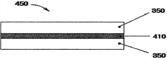
图3是通过在基质层320上形成多层310而制造的多层膜的横截面图350;3 is a
图4是通过使用粘合层410粘附两个多层膜350而制造的多层膜的横截面图450;4 is a
图5是通过在形成于多层膜350或450上的电路层420上形成多层310而制造的电子器件的横截面图550;5 is a
图6是通过在形成于如玻璃和半导体晶片的基质材料430上的电路层420上堆叠多层膜350或450而制造的电子器件的横截面图650;6 is a
图7是根据本发明的实施例1的多层的横截面图,在多沉积层中观察到的,距离为4~5nm的反复形成的无机材料层;7 is a cross-sectional view of a multi-layer according to Example 1 of the present invention, observed in a multi-deposition layer, with a distance of 4-5 nm repeatedly formed inorganic material layers;
图8是根据本发明的实施例2的多层的横截面图;8 is a cross-sectional view of a multilayer according to Embodiment 2 of the present invention;
图9是根据本发明的实施例3的多层的横截面图;以及9 is a cross-sectional view of a multilayer according to Embodiment 3 of the present invention; and
图10是根据本发明的实施例4的多层的横截面图,在多沉积层中观察到的,距离为2~3nm的反复形成的无机材料层。10 is a cross-sectional view of a multi-layer according to Example 4 of the present invention, repeatedly formed inorganic material layers with a distance of 2-3 nm observed in a multi-deposition layer.
具体实施方式 Detailed ways
根据本发明的多层膜包括基质层和设置于基质层的至少一面的多层,所述多层具有两个或多个通过使用单一靶材料形成的子层。A multilayer film according to the present invention includes a substrate layer and a multilayer provided on at least one side of the substrate layer, the multilayer having two or more sublayers formed by using a single target material.
优选的基质层为具有优异柔韧性的基质层。如果需要,为了制造出透明的多层膜,根据其目的,可使用塑料膜,或优选可使用玻璃片、半导体晶片、或复合树脂组合物、或使用金属制备的基质材料。A preferred substrate layer is one having excellent flexibility. If necessary, in order to produce a transparent multilayer film, depending on the purpose, a plastic film may be used, or preferably a glass sheet, a semiconductor wafer, or a composite resin composition, or a matrix material made of a metal may be used.
用于基质层塑料膜的合适材料的例子为选自聚对苯二甲酸乙二醇酯(PET)、聚芳酯、聚醚砜(PES)、聚碳酸酯(PC)、聚萘二甲酸乙二醇酯(PEN)、聚酰亚胺(PI)、聚芳酯和环氧树脂中的一种或多种。Examples of suitable materials for the substrate layer plastic film are selected from the group consisting of polyethylene terephthalate (PET), polyarylate, polyethersulfone (PES), polycarbonate (PC), polyethylene naphthalate One or more of glycol ester (PEN), polyimide (PI), polyarylate and epoxy resin.
为了提高机械性能和热性能,用于基质层的塑料膜可在以下简单填充物或纤维型填充物的协助下形成复合树脂组合物。In order to improve the mechanical and thermal properties, the plastic film used for the matrix layer can form a composite resin composition with the assistance of the following simple fillers or fiber type fillers.
优选的简单填充物的例子包括金属、玻璃粉末、金刚石粉、氧化硅、粘土、磷酸钙、磷酸镁、硫酸钡、氟化铝、硅酸钙、硅酸镁、硅酸钡、碳酸钡、氢氧化钡和硅酸铝。Examples of preferred simple fillers include metal, glass powder, diamond powder, silica, clay, calcium phosphate, magnesium phosphate, barium sulfate, aluminum fluoride, calcium silicate, magnesium silicate, barium silicate, barium carbonate, hydrogen barium oxide and aluminum silicate.
此外,优选的纤维型填充物的例子包括玻璃纤维和玻璃织物纤维。In addition, examples of preferable fibrous fillers include glass fibers and glass woven fibers.
用于基质层的金属的优选例子包括选自不锈钢、铜和铝中的一个或多个。Preferable examples of the metal used for the base layer include one or more selected from stainless steel, copper and aluminum.
由两个或多个子层形成的多层,和2个子层可通过使用一个单一靶材料而不是多个靶材料形成。A multilayer formed of two or more sublayers, and 2 sublayers can be formed by using a single target material instead of multiple target materials.
在这方面,单一靶材料的使用意味着每个子层不是通过使用不同靶材料形成,而是通过使用单一靶材料,例如氮化硅(Si3N4)(但不限于此)的无机靶形成。In this regard, the use of a single target material means that each sublayer is formed not by using a different target material, but by using a single target material, such as an inorganic target of silicon nitride (Si 3 N 4 ) (but not limited thereto). .
通过使用单一靶材料形成的两个子层之间每种元素含量的差异可小于3at%、0~1at%或1~3at%。A difference in content of each element between two sublayers formed by using a single target material may be less than 3 at %, 0˜1 at %, or 1˜3 at %.
由于两个或多个子层通过使用单一靶材料形成,制造过程可以简化。此外,在子层之间元素含量只有很小的差异(3at%或更低),因此减少了易于发生在多层膜之间的剥离。Since two or more sublayers are formed by using a single target material, the manufacturing process can be simplified. In addition, there is only a small difference (3 at % or less) in element content between sublayers, thus reducing the tendency for peeling between multilayer films to occur.
因此,本发明提供的是一种多层膜,其具有优异的气体和水汽阻隔性能以及透光率。Accordingly, the present invention provides a multilayer film having excellent gas and water vapor barrier properties and light transmittance.
用于多层的单一靶材料可包括选自硅、铝、锡、钛、镍、钨、其氧化物、其氮化物及其碳化物中的一种或多种层组成材料。A single target material for multiple layers may include one or more layer constituent materials selected from silicon, aluminum, tin, titanium, nickel, tungsten, oxides thereof, nitrides thereof, and carbides thereof.
每个子层元素组分可包括硅(Si)、氧(O)和氮(N),并进一步包括碳(C)。Each sublayer element composition may include silicon (Si), oxygen (O), and nitrogen (N), and further include carbon (C).
每个子层元素组分可包括硅(Si)和氮(N),且硅(Si)比氮(N)的元素比例(Si/N)可以为1~20。此外,硅(Si)比氮(N)的元素比例(Si/N)可以为1.7~15。Each sub-layer element composition may include silicon (Si) and nitrogen (N), and an element ratio (Si/N) of silicon (Si) to nitrogen (N) may be 1˜20. In addition, an element ratio (Si/N) of silicon (Si) to nitrogen (N) may be 1.7-15.
每个子层元素组分可包括氧(O)和氮(N),且氧(O)比氮(N)的元素比例(O/N)可以为0.1~30。此外,氧(O)比氮(N)的元素比例(O/N)可以为1.4~26。Each sub-layer element composition may include oxygen (O) and nitrogen (N), and an element ratio (O/N) of oxygen (O) to nitrogen (N) may be 0.1˜30. In addition, an element ratio (O/N) of oxygen (O) to nitrogen (N) may be 1.4˜26.
每个子层元素组分可包括氧(O)和硅(Si),且氧(O)比硅(Si)的元素比例(O/Si)可以为0.1~2。此外,氧(O)比硅(Si)的元素比例(O/Si)可以为0.8~1.7。Each sub-layer element composition may include oxygen (O) and silicon (Si), and an element ratio (O/Si) of oxygen (O) to silicon (Si) may be 0.1˜2. In addition, an element ratio (O/Si) of oxygen (O) to silicon (Si) may be 0.8 to 1.7.
每个子层元素组分可包括硅(Si)、氮(N)和氧(O),且硅(Si)比氮(N)的元素比例(Si/N)可以为1~20,且氧(O)比氮(N)的元素比例(O/N)可以为0.1~30。The element composition of each sublayer may include silicon (Si), nitrogen (N) and oxygen (O), and the element ratio (Si/N) of silicon (Si) to nitrogen (N) may be 1-20, and oxygen ( The element ratio (O/N) of O) to nitrogen (N) may be 0.1-30.
每个子层元素组分可包括硅(Si)、氮(N)和氧(O),且硅(Si)比氮(N)的元素比例(Si/N)可以为1.7~15,且氧(O)比氮(N)的元素比例(O/N)可以为1.4~26。Each sublayer element composition may include silicon (Si), nitrogen (N) and oxygen (O), and the element ratio (Si/N) of silicon (Si) to nitrogen (N) may be 1.7-15, and oxygen ( The element ratio (O/N) of O) to nitrogen (N) may be 1.4-26.
每个子层元素组分可包括硅(Si)、氮(N)和氧(O),且硅(Si)比氮(N)的元素比例(Si/N)可以为1~20,氧(O)比氮(N)的元素比例(O/N)可以为0.1~30,且氧(O)比硅(Si)的元素比例(O/Si)可以为0.1~2。The element composition of each sub-layer may include silicon (Si), nitrogen (N) and oxygen (O), and the element ratio (Si/N) of silicon (Si) to nitrogen (N) may be 1 to 20, and oxygen (O The element ratio (O/N) of ) to nitrogen (N) may be 0.1-30, and the element ratio (O/Si) of oxygen (O) to silicon (Si) may be 0.1-2.
每个子层元素组分可包括硅(Si)、氮(N)和氧(O),且硅(Si)比氮(N)的元素比例(Si/N)可以为1.7~15,氧(O)比氮(N)的元素比例(O/N)可以为1.4~26,且氧(O)比硅(Si)的元素比例(O/Si)可以为0.8~1.7。The element composition of each sublayer may include silicon (Si), nitrogen (N) and oxygen (O), and the element ratio (Si/N) of silicon (Si) to nitrogen (N) may be 1.7-15, and oxygen (O The element ratio (O/N) of ) to nitrogen (N) may be 1.4˜26, and the element ratio (O/Si) of oxygen (O) to silicon (Si) may be 0.8˜1.7.
基于组成每个子层的总元素含量,每个子层元素组分可包括30~50at%的硅(Si)、10~65at%的氧(O)和1~50at%的氮(N)。Based on the total element content constituting each sublayer, the element composition of each sublayer may include 30˜50 at % silicon (Si), 10˜65 at % oxygen (O), and 1˜50 at % nitrogen (N).
基于组成每个子层的总元素含量,每个子层元素组分可包括30~50at%的硅(Si)、10~65at%的氧(O)、1~50at%的氮(N)和大于0~5at%的碳(C)。Based on the total element content of each sublayer, the element composition of each sublayer may include 30-50 at% silicon (Si), 10-65 at% oxygen (O), 1-50 at% nitrogen (N) and more than 0 ~5 at% carbon (C).
每个子层可具有由下列公式1表示的氧(O)和氮(N)比硅(Si)为0.5~1的元素比例。Each sublayer may have an element ratio of oxygen (O) and nitrogen (N) to silicon (Si) of 0.5˜1 represented by the following Equation 1.
(公式1)(Formula 1)
(O2+N4/3)/Si(O 2 +N 4/3 )/Si
每个子层可具有0.1nm~50nm的厚度,优选0.5nm~30nm,更优选0.5nm~15nm。Each sublayer may have a thickness of 0.1 nm to 50 nm, preferably 0.5 nm to 30 nm, more preferably 0.5 nm to 15 nm.
两个子层可以具有彼此不同的厚度。The two sublayers may have different thicknesses from each other.
两个或多个子层之中,至少一个子层可具有0.1~50nm的厚度,且其他子层可具有0.1~10nm的厚度。Among the two or more sublayers, at least one sublayer may have a thickness of 0.1 to 50 nm, and the other sublayers may have a thickness of 0.1 to 10 nm.
此外,在两个或多个子层之中,两个具有不同厚度的子层可依次反复堆叠。In addition, among two or more sublayers, two sublayers with different thicknesses may be repeatedly stacked in sequence.
例如,如图7~10所示,具有两个或多个子层的多层可以有厚度范围为0.1~50nm的第一子层、比第一子层薄的厚度范围为0.1~10nm的第二子层、厚度范围为0.1~50nm的第一子层和比第一子层薄的厚度范围为0.1~10nm的第二子层交替堆叠的多层结构。For example, as shown in Figures 7 to 10, a multilayer having two or more sublayers may have a first sublayer with a thickness in the range of 0.1 to 50 nm, a second sublayer thinner than the first sublayer with a thickness in the range of 0.1 to 10 nm. A multilayer structure in which sublayers, first sublayers with a thickness ranging from 0.1 to 50 nm and second sublayers thinner than the first sublayer and with a thickness ranging from 0.1 to 10 nm are stacked alternately.
具有两个或多个子层的多层的厚度可优选根据每个子层的厚度和堆叠数量确定,优选在10nm~5000nm范围内,更优选在10nm~1000nm范围内,且最优选在10nm~300nm范围内。The thickness of a multilayer having two or more sublayers can preferably be determined according to the thickness of each sublayer and the number of stacks, preferably in the range of 10 nm to 5000 nm, more preferably in the range of 10 nm to 1000 nm, and most preferably in the range of 10 nm to 300 nm Inside.
具有两个或多个子层的多层可在基质层的一面或两面上形成,且两个和多个含有根据本发明的多层的多层膜可互相粘附后使用。A multilayer having two or more sublayers can be formed on one or both sides of the substrate layer, and two or more multilayer films containing the multilayer according to the present invention can be used after being adhered to each other.
此外,根据本发明的多层膜可进一步包括涂层,其设置于多层的至少一面上。In addition, the multilayer film according to the present invention may further include a coating layer provided on at least one side of the multilayer.
该涂层可以提高基质层的物理性质,或提供新的性质,如基质层和多层之间粘附的加强、多层膜的机械变形中作用在多层上的应力的迟缓、和防止装运损坏。The coating can improve the physical properties of the substrate layer, or provide new properties, such as enhancement of adhesion between the substrate layer and the multilayer, retardation of stresses acting on the multilayer during mechanical deformation of the multilayer film, and prevention of shipment damage.
该涂层可以使用热固化和/或光固化方法通过选自溶胶凝胶材料、丙烯酸系列、环氧系列、和氨酯系列中的单一材料或一种或多种材料的组合而形成。The coating may be formed by a single material or a combination of one or more materials selected from sol-gel materials, acrylic series, epoxy series, and urethane series using thermal curing and/or photocuring methods.
此外,本发明的多层膜的另一种类型包括一个基质层;和设置于基质层的至少一面上的多层,其中多层具有两个或多个子层的堆叠结构,该子层通过使用选自硅、铝、锡、钛、镍、钨、其氧化物、其氮化物及其碳化物的一种或多种层组成材料形成,且两子层之间的每种元素含量的差异为3at%或更低。其详细说明与以上所提及的相同,因此省略。In addition, another type of the multilayer film of the present invention includes a substrate layer; and a multilayer provided on at least one side of the substrate layer, wherein the multilayer has a stacked structure of two or more sublayers, and the sublayers are obtained by using One or more layer constituent materials selected from silicon, aluminum, tin, titanium, nickel, tungsten, their oxides, their nitrides and their carbides are formed, and the difference in the content of each element between two sublayers is 3at% or less. The detailed description thereof is the same as mentioned above and thus omitted.
根据本发明的多层膜具有优异的气体和水汽阻隔性能以及透光率,因此根据沉积在基质层上的材料,将其制为具有电绝缘性能的基质材料,如,在电泳显示(EPD)、有机发光二极管(OLED)或无机发光器件等中作为基质材料。The multilayer film according to the present invention has excellent gas and water vapor barrier properties and light transmittance, so it is made into a matrix material with electrical insulating properties depending on the material deposited on the matrix layer, e.g., in electrophoretic display (EPD) , organic light-emitting diodes (OLEDs) or inorganic light-emitting devices as matrix materials.
此外,根据本发明的多层膜可用于保护对如水汽和氧气的环境气体敏感的内部电子器件的目的,如需要气体阻隔的EPD、OLED、无机发光器件或产品封装。Furthermore, the multilayer films according to the invention can be used for the purpose of protecting internal electronic devices which are sensitive to ambient gases like water vapor and oxygen, like EPDs, OLEDs, phosphors or product encapsulations requiring a gas barrier.
根据本发明的一种制造该多层膜的方法可以包括通过使用单一靶材料形成两个或多个子层的步骤,以在基质层的至少一面上形成具有两个或多个子层的多层。其详细说明与以上所提及的相同,因此省略。A method of manufacturing the multilayer film according to the present invention may include a step of forming two or more sublayers by using a single target material to form a multilayer having two or more sublayers on at least one side of the substrate layer. The detailed description thereof is the same as mentioned above and thus omitted.
在形成两个或多个子层的步骤中,如果多层不是通过使用多种靶材料形成,而是通过使用单一靶材料由单一步骤形成,则可以简化制造工艺。此外,在子层之间元素含量只有很小的差异(3at%或更低),因此提供了一种具有优异的气体和水汽阻隔性能以及透光率的多层膜。In the step of forming two or more sublayers, if the multilayer is not formed by using a plurality of target materials but is formed in a single step by using a single target material, the manufacturing process can be simplified. In addition, there is only a small difference (3 at % or less) in element content between sublayers, thus providing a multilayer film with excellent gas and water vapor barrier properties and light transmittance.
在不同条件下在同一沉积室使用多靶材料的情况下,靶材料或工艺气体可能很容易相互污染。在本发明中,单一靶材料用于单一步骤。因此,考虑到生产率,即使单一靶材料重复使用,也不会存在由于靶材料和工艺气体条件的差异造成的交叉污染的危险。In cases where multiple target materials are used in the same deposition chamber under different conditions, the target materials or process gases may easily contaminate each other. In the present invention, a single target material is used in a single step. Therefore, considering the productivity, even if a single target material is reused, there is no risk of cross-contamination due to differences in target material and process gas conditions.
此外,在使用单一靶材料形成子层的情况下,由于可在电子显微镜下观察到的子层在元素组分或晶体结构上存在差异,由子层的反复沉积可预期每一次沉积的初始化。也就是说,由于反复堆叠有机和无机物质层,层之间缺陷的生长或扩散由于本发明的微多层结构而被抑制,从而获得了良好的气体阻隔性。In addition, in the case of forming a sublayer using a single target material, since sublayers that can be observed under an electron microscope differ in elemental composition or crystal structure, initialization per deposition can be expected from repeated deposition of sublayers. That is, since layers of organic and inorganic substances are repeatedly stacked, the growth or diffusion of defects between layers is suppressed due to the micromultilayer structure of the present invention, thereby obtaining good gas barrier properties.
具体地说,当两个或多个子层反复堆叠时,在形成层结构的界面产生元素组分(3at%或更低)或微晶结构的差异,该层结构可在电子显微镜下观察到。Specifically, when two or more sublayers are repeatedly stacked, a difference in elemental composition (3 at% or less) or microcrystalline structure occurs at the interface forming the layer structure, which can be observed under an electron microscope.
两个相邻层之间的子层正常堆叠,而起到初始化每次沉积的作用。因此,在使用单一靶材料沉积的过程中,可以预防缺陷的扩散,从而改善了气体阻隔性。因此,在本发明中,微多层结构反复形成以提供具有两个或多个子层的多层。The sublayers between two adjacent layers are stacked normally, which serves to initialize each deposition. Therefore, during deposition using a single target material, diffusion of defects can be prevented, thereby improving gas barrier properties. Therefore, in the present invention, the micromultilayer structure is repeatedly formed to provide a multilayer having two or more sublayers.
可以在氮气和氧气的混合反应气体中使用氮化硅(Si3N4)作为单一靶材料沉积两个或多个子层。Two or more sub-layers can be deposited using silicon nitride (Si 3 N 4 ) as a single target material in a mixed reaction gas of nitrogen and oxygen.
基于总工艺气体,氮气和氧气的混合反应气体可以以大于0和小于60%的比例使用。Based on the total process gas, the mixed reaction gas of nitrogen and oxygen can be used at a ratio of greater than 0 and less than 60%.
混合反应气体中含有的氧气和氮气的比例可能是1∶100~80∶30。考虑到透光率,混合反应气体中含有的氧气和氮气的比例可能是30∶70~75∶25。The ratio of oxygen and nitrogen contained in the mixed reaction gas may be 1:100 to 80:30. In consideration of light transmittance, the ratio of oxygen and nitrogen contained in the mixed reaction gas may be 30:70˜75:25.
形成两个或多个子层的步骤可以在0.5~20mTorr的压力下进行。The step of forming two or more sublayers may be performed under a pressure of 0.5-20 mTorr.
根据本发明的制造多层膜的方法,至少有一个工艺条件,如气流量,处理压力和沉积速率可以根据子层的沉积条件调整,从而改变微多层结构,并将元素组分控制在预定范围内。According to the method for manufacturing a multilayer film of the present invention, at least one process condition, such as gas flow, processing pressure and deposition rate, can be adjusted according to the deposition conditions of the sub-layers, thereby changing the micro-multilayer structure and controlling the elemental composition at a predetermined within range.
该子层优选通过溅射方法、离子镀方法、化学沉积方法、以及溶胶凝胶涂覆方法沉积。但是,为了有效实现本发明的目的,可优选使用溅射方法或离子镀方法。This sublayer is preferably deposited by sputtering methods, ion plating methods, chemical deposition methods, and sol-gel coating methods. However, in order to effectively achieve the object of the present invention, a sputtering method or an ion plating method may be preferably used.
在这方面,调整溅射方法的工艺参数,以控制微观结构、元素组分、构成多层的每个子层的厚度。In this regard, the process parameters of the sputtering method are adjusted in order to control the microstructure, elemental composition, thickness of each sublayer constituting the multilayer.
通过溅射方法沉积若干层的情况下,通常使用相应于沉积层数量的靶材料。然而,在使用单一靶材料的情况下,沉积层的组成可以通过控制反应供料气体的组成改变。例如,在使用如硅、铝、锡、钛、镍、钨等金属的情况下,通过控制溅射工艺中使用的反应气体的类型(例如,氧气,氮气)或浓度,形成并沉积各种无机材料层。此外,在使用碳化物或氮化物作为靶的情况下,工艺气体和其他反应气体(如氧,氨)混合以调整与靶材料的相对反应性,因此,沉积的子层组成可很容易控制。In the case of depositing several layers by sputtering methods, a target material corresponding to the number of deposited layers is generally used. However, in the case of using a single target material, the composition of the deposited layer can be varied by controlling the composition of the reaction feed gas. For example, in the case of using metals such as silicon, aluminum, tin, titanium, nickel, tungsten, etc., by controlling the type (for example, oxygen, nitrogen) or concentration of the reactive gas used in the sputtering process, various inorganic material layer. Furthermore, in the case of using carbide or nitride as targets, the process gas is mixed with other reactive gases (such as oxygen, ammonia) to adjust the relative reactivity with the target material, thus, the deposited sublayer composition can be easily controlled.
根据本发明的溅射方法,除了工艺气体成分,还可调整其他工艺参数如沉积过程中的处理压力、靶的进给能(feeding energy)、沉积的无机材料的冷却条件,沉积设备的几何条件,和沉积时间以控制具有子层的多层的组成。这是因为,调整了工艺参数,从而改变了每个子层的元素组分或微观结构。因此,即使使用单一靶材料并控制工艺参数至单一条件,仍有可能形成由不同子层组成的多层,该不同子层具有不同微无机材料结构和元素组分。According to the sputtering method of the present invention, in addition to the composition of the process gas, other process parameters such as the process pressure during deposition, the feeding energy of the target, the cooling conditions of the deposited inorganic material, the geometrical conditions of the deposition apparatus can be adjusted , and deposition time to control the composition of multiple layers with sublayers. This is because the process parameters are adjusted, thereby changing the elemental composition or microstructure of each sublayer. Therefore, even if a single target material is used and the process parameters are controlled to a single condition, it is still possible to form multilayers composed of different sublayers with different micro-inorganic material structures and elemental compositions.
根据本发明的溅射方法中使用的工艺气体的优选例子包括选自氩气、氦气、氮气(或氨)、氧气、三氟化氮(NF3)、和三氟甲烷(CHF3)中的两个或多个混合反应气体。Preferred examples of the process gas used in the sputtering method according to the present invention include those selected from argon, helium, nitrogen (or ammonia), oxygen, nitrogen trifluoride (NF 3 ), and trifluoromethane (CHF 3 ). Two or more mixed reaction gases.
在这方面,氩气或氦气优选作为基本工艺气体,且至少其他气体作为反应工艺气体与基本工艺气体共同使用。气体进给总量调整在能维持0.5~20mTorr的溅射压力的范围内。基于总工艺气体,混合在工艺气体中的反应气体可以以大于0和小于60%的含量使用,以改变沉积的无机材料的元素组分。例如,压力可保持在0.5~20mTorr范围内,且反应气体混合物的含量可以在大于0和小于35%的范围内,但不限于此。In this respect, argon or helium is preferably used as the basic process gas, and at least one other gas is used together with the basic process gas as a reactive process gas. The total amount of gas feeding is adjusted within the range that can maintain the sputtering pressure of 0.5-20 mTorr. The reactive gas mixed in the process gas can be used at a content greater than 0 and less than 60% based on the total process gas to change the elemental composition of the deposited inorganic material. For example, the pressure may be maintained in the range of 0.5-20 mTorr, and the content of the reaction gas mixture may be in the range of greater than 0 and less than 35%, but not limited thereto.
在上述范围内使用两个或多个的反应气体,例如氧气和氮气,则可以控制沉积的无机材料的元素组分。Using two or more reactive gases within the above range, such as oxygen and nitrogen, can control the elemental composition of the deposited inorganic material.
在溅射工艺中,组成多层的每个子层的厚度根据进给能、气体组成、沉积基质材料的移动速度、和处理压力而变化,且这些参数可以根据沉积系统调节以达到最佳的物理性能(气体阻隔性,透光率等)。In the sputtering process, the thickness of each sublayer that makes up the multilayer varies according to the feed energy, gas composition, moving speed of the deposited matrix material, and process pressure, and these parameters can be adjusted according to the deposition system to achieve the best physical Properties (gas barrier properties, light transmittance, etc.).
在溅射工艺中,组成多层的每个子层的元素组分可根据靶材料的类型、反应气体的类型和浓度、处理压力、和靶的进给能而变化。In a sputtering process, the elemental composition of each sublayer making up a multilayer may vary depending on the type of target material, the type and concentration of reactive gas, process pressure, and feed energy of the target.
在溅射工艺中,组成多层的每个子层的微观结构可根据进给能、沉积工艺过程中沉积层的冷却条件和层中的元素组分而变化。特别的,关于冷却条件,沉积系统可以配备额外的冷却装置,以便于在沉积工艺过程中或其后控制沉积层的冷却。In the sputtering process, the microstructure of each sublayer that makes up the multilayer can vary depending on the feed energy, the cooling conditions of the deposited layer during the deposition process, and the elemental composition in the layer. In particular, regarding cooling conditions, the deposition system can be equipped with additional cooling devices in order to control the cooling of the deposited layer during or after the deposition process.
溅射可优选控制主要工艺参数,如靶的进给能、基质材料的移动速度(或基质材料的冷却速度)、处理压力、以及工艺气体的流量和组成。Sputtering may preferably control key process parameters such as target feed energy, matrix material movement rate (or matrix material cooling rate), process pressure, and process gas flow and composition.
以下,根据本发明的制造多层膜的方法将参考附图详细描述。Hereinafter, a method of manufacturing a multilayer film according to the present invention will be described in detail with reference to the accompanying drawings.
图1是沉积系统150的原理图,其可用于通过溅射方法制造根据本发明的多层。在沉积设备150中,靶131固定在基质材料120上方,且通过电源132向其供电。基质材料120放置在传送带121上,并通过一对辊141和142的旋转左右移动。辊141和142的旋转速度在左右方向上是可控的,基质材料的移动距离在靶下方左右方向上可变,且基质材料120在传送带121的两端的停留时间可任意控制。Figure 1 is a schematic diagram of a
图2是改进的沉积设备250的原理图,该设备通过在辊141和142改进图1的设备150为一个连续膜工艺而制造,其中改进的系统在移动基质材料下方装备了具有冷却装置220,以在沉积工艺过程中或其后控制沉积层的冷却条件。此外,在使用配备了两个或多个靶的沉积系统(150或250)的情况下,有可能形成具有不同微多层结构的多层。FIG. 2 is a schematic diagram of a modified
图3显示了通过在基质层320上形成由几个子层组成的多层310而制造的多层膜350的横截面图。FIG. 3 shows a cross-sectional view of a
图4显示了通过使用一个粘合层410粘附两个多层膜350而制造的多层膜450的横截面图。FIG. 4 shows a cross-sectional view of a
图5显示了通过在形成于多层膜350或450上的电路层420上形成多层310而制造的电子器件550的横截面图。FIG. 5 shows a cross-sectional view of an
图6显示了通过在形成于如玻璃和半导体晶片的基质材料430上的电路层420上堆叠多层膜350或450而制造的电子器件650的横截面图;6 shows a cross-sectional view of an
本发明提供了含有多层膜的发光器件、显示器件、或太阳能电池器件。The present invention provides a light emitting device, a display device, or a solar cell device comprising a multilayer film.
实施例Example
以下将根据实施例详细描述本发明。但是,本发明可以以许多不同的形式实施,且本发明不应该被解释为限于以下所述的实施例。相反,这些实施例的提供意味着本公开向所属领域技术人员全面彻底,并且充分表达了本发明的概念。Hereinafter, the present invention will be described in detail based on examples. However, the present invention can be embodied in many different forms, and the present invention should not be construed as being limited to the embodiments described below. Rather, these embodiments are provided to mean that this disclosure is thorough and thorough, and fully conveys the concept of the invention to those skilled in the art.
<实施例1~4><Examples 1 to 4>
通过溅射单一氮化硅(Si3N4)在100μm厚的PET基质层上沉积一个多层。在如表1所示的不同的工艺气体组成和处理压力下进行实施例1~4,且在每个实施例的沉积工艺过程中,工艺气体的组分保持在表1中所示的比例。共同的工艺条件如下:加载到靶上的电能为2kW,基于总的工艺气体,氧气和氮气的混合反应气体的浓度保持在20%,并调整靶下方每个方向上的基质材料的移动距离。A multilayer was deposited by sputtering a single silicon nitride (Si 3 N 4 ) layer on a 100 μm thick PET substrate layer. Examples 1-4 were performed under different process gas compositions and process pressures as shown in Table 1, and during the deposition process of each example, the components of the process gas were maintained at the ratios shown in Table 1. The common process conditions are as follows: the electric power loaded on the target is 2kW, the concentration of the mixed reaction gas of oxygen and nitrogen is kept at 20% based on the total process gas, and the moving distance of the matrix material in each direction under the target is adjusted.
<对比实施例1和2><Comparative Examples 1 and 2>
在对比实施例1中,沉积了没有多层的基质层,以及在对比实施例2中,通过在保持基于总的工艺气体中氧气浓度为10%,和进给能为2kW的条件下溅射SiO2靶制造了多层膜。In Comparative Example 1, a matrix layer without multiple layers was deposited, and in Comparative Example 2, by sputtering while maintaining an oxygen concentration of 10% based on the total process gas, and a feed energy of 2 kW SiO 2 targets fabricated multilayer films.
<实验实施例1>透湿性和透光率的测量<Experimental Example 1> Measurement of moisture permeability and light transmittance
为了评估本发明的多层的性能,测量了每个多层的透湿性和透光率。透湿性用水蒸气渗透性测试仪(L80-5000,Lyssy)在38℃、保持膜两面的湿度差异90%RH下测量,以及透光率是用分光光度计测量(Cary 3E,Varian)。多层的横截面用透射电子显微镜(TEM,TECHNAI 20-S,飞利浦)分析。测量的结果呈现于下表1。In order to evaluate the performance of the multilayers of the present invention, the moisture permeability and light transmittance of each multilayer were measured. Moisture permeability was measured with a water vapor permeability tester (L80-5000, Lyssy) at 38°C, maintaining a humidity difference of 90% RH on both sides of the film, and light transmittance was measured with a spectrophotometer (Cary 3E, Varian). The cross-sections of the multilayers were analyzed with a transmission electron microscope (TEM, TECHNAI 20-S, Philips). The results of the measurements are presented in Table 1 below.
【表1】【Table 1】

如表1所示,实施例1~3中所制造的多层膜被发现具有测试仪器检测极限以下的透湿性,且根据溅射条件下可保持优异的透光率。图7~10显示了使用透射电子显微镜(TEM)观察的实施例1~4中沉积的多层的横截面,其中多层通过反复堆叠2~5nm厚的薄成分层形成,即使在每种情况下使用的是单一靶和单一气体条件。As shown in Table 1, the multilayer films produced in Examples 1-3 were found to have moisture permeability below the detection limit of the testing instrument, and could maintain excellent light transmittance under sputtering conditions. 7 to 10 show the cross-sections of the multilayers deposited in Examples 1 to 4 observed using a transmission electron microscope (TEM), where the multilayers are formed by repeatedly stacking thin component layers with a thickness of 2 to 5 nm, even in each case A single target and single gas condition was used below.
<实验实施例2>多层的元素分析和水接触角的测量<Experimental Example 2> Elemental analysis of multiple layers and measurement of water contact angle
使用XPS(X射线光电子能谱,ESCA Lab 250 System)进行根据实施例1~4的多层的元素分析,其结果如表2~4所示。为评价根据实施例1~4的多层的表面性质,测量其水滴接触角,其结果如表2所示。Use XPS (X-ray Photoelectron Spectroscopy,
【表2】【Table 2】

【表3】【table 3】

【表4】【Table 4】

※表3和表4是通过反复氩离子蚀刻以消除因暴露于大气中产生的杂质而进行的XPS元素分析的结果,其中时间点(秒)表示氩离子蚀刻在预定条件下经过的时间段,且在每个时间点进行元素分析。※Table 3 and Table 4 are the results of XPS elemental analysis performed by repeated argon ion etching to eliminate impurities generated by exposure to the atmosphere, where the time points (seconds) indicate the period of time elapsed by argon ion etching under predetermined conditions, And elemental analysis was performed at each time point.
如表2的水滴接触角所示,多层的表面性质可通过改变工艺条件控制。As shown by the water droplet contact angles in Table 2, the surface properties of the multilayers can be controlled by changing the process conditions.
此外,如表2所示,组成根据本发明的实施例1~4的多层的子层被发现具有硅、氧、氮或氧、氮、硅、碳的元素组分,说明多层的元素组分可通过调整工艺条件控制。In addition, as shown in Table 2, the sublayers constituting the multilayers according to Examples 1 to 4 of the present invention were found to have elemental components of silicon, oxygen, nitrogen or oxygen, nitrogen, silicon, carbon, indicating that the elemental composition of the multilayers Components can be controlled by adjusting process conditions.
如表3~表4所示,其为在每个时间点分析元素组分的结果,当通过使用单一靶材料形成组成实施例1~4的多层的两个或多个子层时,经过10秒或更长时间的蚀刻,子层之间的元素组分的差异保持在误差范围内。As shown in Tables 3 to 4, which are the results of analyzing elemental components at each time point, when two or more sublayers of the multilayers of Examples 1 to 4 are formed by using a single target material, after 10 The difference in elemental composition between sublayers remains within the error range for etching times of seconds or longer.
因此,当具有两个或多个子层的多层不是通过使用多个靶材料形成,而是通过使用单一靶材料和单一的一套工艺条件形成时,通过使用单一靶材料形成的两个或多个子层之间的元素含量仅有微小的差异(3at%或更低),从而提供一种具有优异的气体和水汽阻隔性能以及透光率的多层膜。Therefore, when a multilayer having two or more sublayers is formed not by using a plurality of target materials but by using a single target material and a single set of process conditions, two or more sublayers formed by using a single target material There are only slight differences (3 at% or less) in element content between the sublayers, thereby providing a multilayer film with excellent gas and water vapor barrier properties and light transmittance.
Claims (35)
Applications Claiming Priority (3)
| Application Number | Priority Date | Filing Date | Title |
|---|---|---|---|
| KR10-2007-0053767 | 2007-06-01 | ||
| KR20070053767 | 2007-06-01 | ||
| PCT/KR2008/003091 WO2008147163A1 (en) | 2007-06-01 | 2008-06-02 | Multiple-layer film and method for manufacturing the same |
Publications (2)
| Publication Number | Publication Date |
|---|---|
| CN101743267A CN101743267A (en) | 2010-06-16 |
| CN101743267B true CN101743267B (en) | 2013-12-25 |
Family
ID=40075297
Family Applications (1)
| Application Number | Title | Priority Date | Filing Date |
|---|---|---|---|
| CN2008800184845A Active CN101743267B (en) | 2007-06-01 | 2008-06-02 | Multiple-layer film and method for manufacturing same |
Country Status (6)
| Country | Link |
|---|---|
| US (1) | US20100279092A1 (en) |
| EP (1) | EP2152786B1 (en) |
| JP (1) | JP5419868B2 (en) |
| KR (1) | KR101019061B1 (en) |
| CN (1) | CN101743267B (en) |
| WO (1) | WO2008147163A1 (en) |
Families Citing this family (7)
| Publication number | Priority date | Publication date | Assignee | Title |
|---|---|---|---|---|
| JP5381734B2 (en) * | 2010-01-14 | 2014-01-08 | コニカミノルタ株式会社 | Barrier film and organic electronic device |
| US9991399B2 (en) | 2012-10-04 | 2018-06-05 | Cree, Inc. | Passivation structure for semiconductor devices |
| US9812338B2 (en) * | 2013-03-14 | 2017-11-07 | Cree, Inc. | Encapsulation of advanced devices using novel PECVD and ALD schemes |
| US8994073B2 (en) | 2012-10-04 | 2015-03-31 | Cree, Inc. | Hydrogen mitigation schemes in the passivation of advanced devices |
| JP6030815B1 (en) * | 2015-04-28 | 2016-11-24 | 三井金属鉱業株式会社 | Surface-treated copper foil and method for producing the same, copper-clad laminate for printed wiring board, and printed wiring board |
| CN109411417B (en) | 2017-08-18 | 2020-09-11 | 财团法人工业技术研究院 | Electronic component package and display panel |
| KR20200125852A (en) | 2019-04-26 | 2020-11-05 | 조규찬 | The double screw system of discharge that discharges liquid substances only by a quantitative amount |
Citations (3)
| Publication number | Priority date | Publication date | Assignee | Title |
|---|---|---|---|---|
| US5876788A (en) * | 1997-01-16 | 1999-03-02 | International Business Machines Corporation | High dielectric TiO2 -SiN composite films for memory applications |
| CN1695257A (en) * | 2002-09-11 | 2005-11-09 | 通用电气公司 | Diffusion barrier coatings having graded compositions and devices incorporating the same |
| WO2006082794A1 (en) * | 2005-02-01 | 2006-08-10 | Mitsui Chemicals, Inc. | Method for joining members, composite film and use thereof |
Family Cites Families (22)
| Publication number | Priority date | Publication date | Assignee | Title |
|---|---|---|---|---|
| JP3684593B2 (en) * | 1993-07-28 | 2005-08-17 | 旭硝子株式会社 | Sputtering method and apparatus |
| JP3634460B2 (en) * | 1995-10-03 | 2005-03-30 | 株式会社神戸製鋼所 | Coating film excellent in halogen-based gas corrosion resistance and halogen-based plasma corrosion resistance, and laminated structure provided with the coating film |
| JPH10160902A (en) * | 1996-11-27 | 1998-06-19 | Sony Corp | Antireflection film, its forming method and forming device |
| KR100275389B1 (en) * | 1997-01-16 | 2000-12-15 | 포만 제프리 엘 | High dielectric tio2-sin composite films for memory applications |
| JP2000026139A (en) * | 1998-07-06 | 2000-01-25 | Nippon Sheet Glass Co Ltd | Coating method with insulating film and glass substrate for image display using same |
| EP1145338B1 (en) * | 1998-12-16 | 2012-12-05 | Samsung Display Co., Ltd. | Environmental barrier material for organic light emitting device and method of making |
| EP1054456A3 (en) * | 1999-05-17 | 2007-01-03 | Dai Nippon Printing Co., Ltd. | Protective sheet for solar battery module, method of fabricating the same and solar battery module |
| JP2002100469A (en) * | 2000-09-25 | 2002-04-05 | Pioneer Electronic Corp | Organic electroluminescence display panel |
| JP2003093896A (en) * | 2001-07-19 | 2003-04-02 | Toto Ltd | Method for forming photocatalyst titanium oxide film |
| JP3859518B2 (en) * | 2002-01-15 | 2006-12-20 | 住友ベークライト株式会社 | Transparent water vapor barrier film |
| US20040121146A1 (en) * | 2002-12-20 | 2004-06-24 | Xiao-Ming He | Composite barrier films and method |
| JP4261902B2 (en) * | 2002-12-26 | 2009-05-13 | 大日本印刷株式会社 | Barrier film and laminate using the same, packaging container, image display medium, and barrier film manufacturing method |
| TWI370700B (en) * | 2003-03-31 | 2012-08-11 | Dainippon Printing Co Ltd | Protective coat and method for manufacturing thereof |
| JP2004330623A (en) * | 2003-05-08 | 2004-11-25 | Teijin Ltd | Gas barrier polymer laminated film suitable for display |
| US7635525B2 (en) * | 2003-09-30 | 2009-12-22 | Fujifilm Corporation | Gas barrier laminate film and method for producing the same |
| JP4589128B2 (en) * | 2004-03-09 | 2010-12-01 | 大日本印刷株式会社 | Gas barrier film that prevents bending |
| JP4593213B2 (en) * | 2004-09-14 | 2010-12-08 | 大日本印刷株式会社 | Gas barrier plastic container and manufacturing method thereof |
| JP2006123306A (en) * | 2004-10-28 | 2006-05-18 | Dainippon Printing Co Ltd | Gas barrier laminate |
| JP4698310B2 (en) * | 2005-07-11 | 2011-06-08 | 富士フイルム株式会社 | Gas barrier film, substrate film and organic electroluminescence device |
| JP4279816B2 (en) | 2005-09-02 | 2009-06-17 | 国立大学法人北陸先端科学技術大学院大学 | Transparent gas barrier substrate |
| JP4763400B2 (en) * | 2005-09-22 | 2011-08-31 | 株式会社巴川製紙所 | Clay thin film substrate, clay thin film substrate with electrode, and display element using them |
| JP4717674B2 (en) * | 2006-03-27 | 2011-07-06 | 富士フイルム株式会社 | Gas barrier film, substrate film and organic electroluminescence device |
-
2008
- 2008-06-02 JP JP2010510232A patent/JP5419868B2/en active Active
- 2008-06-02 WO PCT/KR2008/003091 patent/WO2008147163A1/en active Application Filing
- 2008-06-02 EP EP08766053.6A patent/EP2152786B1/en active Active
- 2008-06-02 US US12/451,778 patent/US20100279092A1/en not_active Abandoned
- 2008-06-02 KR KR1020080051838A patent/KR101019061B1/en active IP Right Grant
- 2008-06-02 CN CN2008800184845A patent/CN101743267B/en active Active
Patent Citations (3)
| Publication number | Priority date | Publication date | Assignee | Title |
|---|---|---|---|---|
| US5876788A (en) * | 1997-01-16 | 1999-03-02 | International Business Machines Corporation | High dielectric TiO2 -SiN composite films for memory applications |
| CN1695257A (en) * | 2002-09-11 | 2005-11-09 | 通用电气公司 | Diffusion barrier coatings having graded compositions and devices incorporating the same |
| WO2006082794A1 (en) * | 2005-02-01 | 2006-08-10 | Mitsui Chemicals, Inc. | Method for joining members, composite film and use thereof |
Non-Patent Citations (2)
| Title |
|---|
| JP特开2002-100469A 2002.04.05 |
| JP特开2004-330623A 2004.11.25 |
Also Published As
| Publication number | Publication date |
|---|---|
| KR101019061B1 (en) | 2011-03-07 |
| JP5419868B2 (en) | 2014-02-19 |
| JP2010528894A (en) | 2010-08-26 |
| EP2152786A1 (en) | 2010-02-17 |
| US20100279092A1 (en) | 2010-11-04 |
| EP2152786A4 (en) | 2012-03-07 |
| WO2008147163A1 (en) | 2008-12-04 |
| EP2152786B1 (en) | 2016-08-17 |
| KR20090004491A (en) | 2009-01-12 |
| CN101743267A (en) | 2010-06-16 |
Similar Documents
| Publication | Publication Date | Title |
|---|---|---|
| CN101743267B (en) | Multiple-layer film and method for manufacturing same | |
| US20240288610A1 (en) | Multi-layer wet-dry hardcoats for flexible cover lens | |
| US8133577B2 (en) | Silicon-nitrogen compound film, and gas-barrier film and thin-film device using the silicon-nitrogen compound film | |
| US7074501B2 (en) | Coatings with low permeation of gases and vapors | |
| WO2020263633A1 (en) | Flexible multi-layered cover lens stacks for foldable displays | |
| JP3859518B2 (en) | Transparent water vapor barrier film | |
| KR20130025969A (en) | Transparent conductive film and manufacturing method therefor | |
| KR20150041061A (en) | Articles including a (co)polymer reaction product of a urethane (multi)-(meth)acrylate (multi)-silane | |
| JP2007526601A (en) | Diffusion barrier layer and method for producing diffusion barrier layer | |
| US8975534B2 (en) | Flexible base material and flexible electronic device | |
| CN110168135B (en) | Hard coating system and method for producing a hard coating system in a continuous roll-to-roll process | |
| Lee et al. | Environmental reliability and moisture barrier properties of silicon nitride and silicon oxide films using roll-to-roll plasma enhanced chemical vapor deposition | |
| US10961622B2 (en) | Gas barrier film and method of manufacturing the same | |
| TWI700180B (en) | Laminated body and gas barrier film | |
| JP4506365B2 (en) | Barrier film manufacturing method | |
| CN107428126B (en) | Laminate and gas barrier film | |
| TWI703614B (en) | Barrier layer system, electro-optical device having the same, and method for manufacturing a barrier layer system in a continuous roll-to-roll process | |
| JP2005059211A (en) | Gas barrier base material | |
| Kimmel et al. | 10.2: High‐Performance Barrier Films for Flexible Organic Display and Lighting Applications | |
| WO2015141741A1 (en) | Electronic device | |
| JP2004001356A (en) | Transparent steam barrier film sheet and its manufacturing method |
Legal Events
| Date | Code | Title | Description |
|---|---|---|---|
| C06 | Publication | ||
| PB01 | Publication | ||
| C10 | Entry into substantive examination | ||
| SE01 | Entry into force of request for substantive examination | ||
| C14 | Grant of patent or utility model | ||
| GR01 | Patent grant |