CN101681667B - Sense amplifier with stages to reduce capacitance mismatch in current mirror load - Google Patents
Sense amplifier with stages to reduce capacitance mismatch in current mirror load Download PDFInfo
- Publication number
- CN101681667B CN101681667B CN200880002070.3A CN200880002070A CN101681667B CN 101681667 B CN101681667 B CN 101681667B CN 200880002070 A CN200880002070 A CN 200880002070A CN 101681667 B CN101681667 B CN 101681667B
- Authority
- CN
- China
- Prior art keywords
- output node
- transistor
- node
- current
- coupled
- Prior art date
- Legal status (The legal status is an assumption and is not a legal conclusion. Google has not performed a legal analysis and makes no representation as to the accuracy of the status listed.)
- Expired - Fee Related
Links
Images


Classifications
-
- G—PHYSICS
- G11—INFORMATION STORAGE
- G11C—STATIC STORES
- G11C7/00—Arrangements for writing information into, or reading information out from, a digital store
- G11C7/06—Sense amplifiers; Associated circuits, e.g. timing or triggering circuits
- G11C7/062—Differential amplifiers of non-latching type, e.g. comparators, long-tailed pairs
-
- G—PHYSICS
- G11—INFORMATION STORAGE
- G11C—STATIC STORES
- G11C16/00—Erasable programmable read-only memories
- G11C16/02—Erasable programmable read-only memories electrically programmable
- G11C16/06—Auxiliary circuits, e.g. for writing into memory
- G11C16/26—Sensing or reading circuits; Data output circuits
- G11C16/28—Sensing or reading circuits; Data output circuits using differential sensing or reference cells, e.g. dummy cells
-
- G—PHYSICS
- G11—INFORMATION STORAGE
- G11C—STATIC STORES
- G11C7/00—Arrangements for writing information into, or reading information out from, a digital store
- G11C7/06—Sense amplifiers; Associated circuits, e.g. timing or triggering circuits
- G11C7/067—Single-ended amplifiers
-
- G—PHYSICS
- G11—INFORMATION STORAGE
- G11C—STATIC STORES
- G11C2207/00—Indexing scheme relating to arrangements for writing information into, or reading information out from, a digital store
- G11C2207/06—Sense amplifier related aspects
- G11C2207/063—Current sense amplifiers
Landscapes
- Read Only Memory (AREA)
- Static Random-Access Memory (AREA)
- Mram Or Spin Memory Techniques (AREA)
Abstract
Description
技术领域 technical field
本发明涉及从存储器读取数据,且更明确地说,涉及用于存储器单元的读取电路,在其中对单元电流与参考电流进行比较。The present invention relates to reading data from a memory, and more particularly to a read circuit for a memory cell in which the cell current is compared to a reference current.
背景技术 Background technique
读出放大器是通常包含于电子装置中的存储器组件中且完成存储器中的存储器单元的状态的读取的电子电路。此读取过程取决于在明确界定的偏置条件下存储器单元吸收多少电流。读出放大器的任务是将此电流信息变换成适于用作内部数字存储器数据的二进制信息。在最简单的情况下,二进制信息由两个逻辑电平(“1”或“0”)组成,所述逻辑电平分别对应于其中在明确界定的偏置条件下单元吸收电流或不吸收电流的存储器单元状态。A sense amplifier is an electronic circuit typically included in a memory component in an electronic device and that performs the reading of the state of the memory cells in the memory. This read process depends on how much current the memory cell sinks under well-defined bias conditions. The task of the sense amplifier is to transform this current information into binary information suitable for use as internal digital memory data. In the simplest case, binary information consists of two logic levels ("1" or "0") corresponding to where the cell sinks current or does not sink current under well-defined bias conditions, respectively. state of the memory cell.
读取单元状态的一种方法是将单元电流(Icell)与通常由另一单元提供的参考电流(Iref)进行比较,且跟踪存储器单元的过程特性。参考单元通常吸收具有位于逻辑状态“1”下的单元电流与逻辑状态“0”下的单元电流之间的值的电流。举例来说,如果处于状态“0”的存储器单元不吸收电流,那么参考单元可吸收逻辑状态“1”下的单元电流的一半。读出放大器读取单元电流与参考电流之间的差,将所述差变换成适合由其它存储器芯片电路使用的二进制信息。举例来说,如果单元状态为“1”或“0”,那么电流差可分别为正或负,使得读出放大器分别产生二进制信号“1”或“0”。One method of reading the state of a cell is to compare the cell current (I cell ) to a reference current (I ref ), typically provided by another cell, and track the memory cell's process characteristics. A reference cell typically sinks a current having a value between the cell current in a logic state "1" and the cell current in a logic state "0." For example, if a memory cell in state "0" sinks no current, a reference cell may sink half the current of a cell in logic state "1." A sense amplifier reads the difference between the cell current and the reference current, transforming the difference into binary information suitable for use by other memory chip circuits. For example, if the cell state is "1" or "0," then the current difference can be positive or negative, respectively, so that the sense amplifier produces a binary signal of "1" or "0," respectively.
图1说明用于读出放大器系统10的常规方案。元件500、600、530和630并非读出放大器自身的部分,但这些元件示意性地描绘单元存储器阵列。存储器单元500是想要知晓其状态的单元,且提供参考单元600作为参考。这些单元通常分别通过位线530和630而链接到读出放大器电路。为了允许单元500和600传导其电流,必须使栅极510和610以及漏极520和620的电压达到适宜的电压值。明确地说,漏极电压是由读出放大器电路使用由反相器310和410构成的反馈配置来设置的。在其它实施例中,可使用其它方法来确保漏极电压的正确极化。反相器确保适宜的电压值(例如,约1V)被设置于分别位于位线530和630的末端处的节点540和640上以及节点520和620上。由启用信号710控制的传递栅极700仅在被称为“均衡阶段”的初始瞬变周期内使节点800和900保持在同一电压值。在此阶段期间,晶体管200设置节点900的电压,且经由传递栅极700使用晶体管100,还设置节点800的电压。实际上,由于晶体管200处于二极管配置,所以其栅极到源极电压与漏极电流之间存在明确界定的关系:FIG. 1 illustrates a conventional scheme for a
其中Ids是漏极到源极电流,μ是载流子迁移率,Cox是每单位面积的栅极氧化物电容,W和L分别是晶体管的宽度和长度,Vgs是栅极到源极电压,且Vth是阈值电压。对于给定Ids,节点900的电压值是确定的,因为其值与如出现在等式(1)中的晶体管200的Vgs相符。where Ids is the drain-to-source current, μ is the carrier mobility, Cox is the gate oxide capacitance per unit area, W and L are the width and length of the transistor, respectively, and Vgs is the gate-to-source pole voltage, and V th is the threshold voltage. For a given I ds , the voltage value of
现在针对“稳定状态”条件而呈现对电路的第一简化分析,其中所有电流和电压都是固定的。一旦达到此状态,晶体管300和400就分别吸收单元电流和参考电流。晶体管100和200构成众所周知的镜像配置,即,穿过晶体管200的所有电流全部被转移到晶体管100。一旦传递栅极700断开,晶体管200就供应参考单元电流经过晶体管400。晶体管200又通过晶体管100将参考单元电流转移到电路的另一侧。节点800接收来自晶体管100的参考电流和来自晶体管300的单元电流。因此,从在均衡阶段期间由晶体管200固定的电压开始,节点800逐渐演变为由电流差(Iref-Icell)驱动,遵循此简单定律:A first simplified analysis of the circuit is now presented for a "steady state" condition, where all currents and voltages are fixed. Once this state is reached,
其中ΔV800是由电流差(Iref-Icell)对节点800的寄生电容(称为C800)进行充电或放电经过时间ΔT后而得到的电压差。C800是耦合到节点800的晶体管的寄生电容加上组件连接的互连金属的寄生电容的和。值得注意的是,在等式(2)中,对于此简化分析,假定Iref和Icell是不随时间而变化的,因为推测已达到稳定状态条件。节点900的电压电平准确地表示参考电流,因为根据等式(1),节点的值直接取决于Iref值,而节点800的电压电平准确地表示单元电流,因为取决于单元电流值,节点800相对于其起始值而被充电或放电。如果为简单起见而将C800称为Cout,那么用于Vout的等式变为:Wherein ΔV 800 is the voltage difference obtained after the current difference (I ref −I cell ) charges or discharges the parasitic capacitance of node 800 (called C 800 ) for a time ΔT. C 800 is the sum of the parasitic capacitance of the transistor coupled to
如果电路正感测“0”,那么Vout具有正号,如果正感测“1”,那么Vout具有负号,且Vout的量值随时间而增长。此电压差适合用作比较器1000的输入,比较器1000将此电压差放大,以便具有满幅信号(即,GND或Vdd)。信号的经放大形式提供所需的二进制信息,且适合用于内部二进制数据交换;按照惯例,处于Vdd或GND的满幅信号分别对应于逻辑电平“1”或“0”。If the circuit is sensing a "0" then V out has a positive sign, if it is sensing a "1" then V out has a negative sign and the magnitude of V out increases over time. This voltage difference is suitable for use as an input to
上述分析是针对其中仅稳定状态电流经过晶体管的简单情况。遗憾的是,稳定状态条件可能要花费较长时间才能达到,尤其是在高电容性位线将单元链接到读出放大器电路且单元电流非常低的情况下。在被称为“预充电阶段”(其在来自主路径晶体管的电流开始对位线进行充电时开始,且一旦预充电电流变为相对于单元电流来说为可忽略时就结束)的瞬变周期期间,电流穿过位线,以将单元的漏极提升到所要的电压电平(约1V)。此阶段必须花费尽可能短的时间;因此,晶体管100、200、300和400的宽度必须足够大,以从Vdd供应所有所需的预充电电流。在所述阶段开始时,此电流达到与位线电容值成正比例的峰值,且接着所述电流降落到零,且仅稳态电流穿过晶体管300和400。一旦传递栅极700断开,节点800就以与C800的值成反比的速度改变(如等式(2)所描绘)。由于晶体管100和300可能相当大,所以C800也可能相当大,且节点800可能无法足够快地改变而允许系统的所要读取性能。此外,电流差(Iref-Icell)可能非常小,从而以非常低的强度来驱动节点800。总之,这种简单的读出放大器方案可能不适合于以快速方式来读取数据,尤其是在其中较长的位线将单元链接到读出放大器电路且电流差(Iref-Icell)非常小的情况下。The above analysis is for the simple case where only steady state current passes through the transistor. Unfortunately, steady-state conditions can take a long time to reach, especially in cases where a highly capacitive bit line links the cell to the sense amplifier circuit and the cell current is very low. Transient during what is known as the "precharge phase" which begins when the current from the main path transistor begins to charge the bit line and ends once the precharge current becomes negligible relative to the cell current During a cycle, current is passed through the bit line to boost the cell's drain to the desired voltage level (approximately 1V). This phase must take as short a time as possible; therefore, the width of
图2中展示用于读出放大器系统20的另一方法。将折叠级添加到图1的系统,以改进在均衡阶段后输出节点的演变速度。晶体管100和110与晶体管200和210成镜像配置,其中穿过晶体管100和200的电流分别由晶体管110和210转移到折叠级。在均衡阶段期间,晶体管220根据等式(1)来设置节点910的电压值,且经由传递栅极700,连同晶体管120一起,还设置节点810的电压。一旦达到稳定状态,晶体管210和110就分别向折叠级供应参考电流和单元电流。当传递栅极700断开时,节点810经由晶体管110接收单元电流,且由于晶体管220和120成镜像配置,而经由晶体管120接收参考电流。节点810因此逐渐演变为由如由以下等式描绘的电流差(Iref-Icell)驱动:Another approach for
节点810的演变速度取决于其电容C810的值。等式(4)类似于描绘图1中的方案的行为的等式(2);因此,为获得相对于先前方案的改进,C810必须比等式(2)中出现的C800小得多。不管互连金属,C810的主要分量是由于与节点810耦合的晶体管110和120的寄生电容而引起的。这些晶体管越小,节点的电容性就越小。因为晶体管110转移折叠级中的单元电流,所以过多地减小晶体管110的大小是不合宜的:如果(例如)110比100小n倍,那么折叠级中所转移的电流将小n倍,因为110和100是两个镜像连接晶体管。这是不可取的,因为Icell的值可能非常小。代替地,有可能提供较小的晶体管120,因为其不必供应如由主电路路径中的晶体管供应的预充电电流。节点810接着可在电容方面比节点800低很多,且当传递栅极700断开时,节点810可比图1中的电路的节点800更快地演变。如果为简单起见将C810称为Cf,out,那么用于Vout的等式变为:The speed at which
其中Cf,out比等式(3)中出现的Cout小很多。如果电路感测“1”,那么Vout具有正号,如果电路感测“0”,那么Vout具有负号。where C f,out is much smaller than C out appearing in equation (3). If the circuit senses a "1" then V out has a positive sign and if the circuit senses a "0" then V out has a negative sign.
然而,图2的方案具有涉及其自身的折叠级的瞬变行为的其它问题。在位线预充电阶段期间,晶体管100和200分别向晶体管110和210供应单元电流和参考电流(Icell和Iref),加上对应的位线预充电电流或(在更一般的情况下)任何其它瞬变电流。即使在传递栅极700断开时,来自主电路的单元侧和参考侧的总电流也可能由于所有上文所提及的瞬变电流而随时间改变。因此,晶体管220必须不断地调适其偏置条件以引导所供应的电流,从而将所供应的电流转移到镜像连接晶体管120。根据等式(1),晶体管220的栅极到源极电压必须适应从晶体管210注入的电流。因此,节点910的寄生电容(称为C910)必须被充电或放电,以便达到正确的偏置条件。这产生与节点910上的电荷转移有关的杂散电流分量(称为IC910)。由于晶体管220和120成镜像配置,所以电流IC910被供应到节点810,节点810逐渐演变为也由此电流分量驱动。将分别从主电路的单元侧和参考侧供应的总电流称为Icell,side(Icell加上任何瞬变电流)和Iref,side(Iref加上任何瞬变电流),用于节点810的等式变为:However, the scheme of Fig. 2 has other problems related to the transient behavior of its own folding stage. During the bitline precharge phase,
值得注意的是,因为等式(6)中的所有项都随时间而变化(为简单起见,忽略电容C810由于晶体管110和120的不同偏置条件而也随时间变化的事实),所以需要所述等式中的积分形式。还应指出,来自主电路(包含晶体管100或200)的任何瞬变电流的确切行为以及其对读取性能的影响不在此分析的范围内。从上述等式开始,有可能将分析集中在电容性电流分量IC910的影响下的折叠电路行为。如等式(6)所示,后一项是可能引起不正确数据读取的唯一电流分量(取决于折叠级自身)。此电流是由某一瞬变行为产生的,且接着在稳定状态下所述电流减小到零。此杂散电流分量可破坏从单元获取的正确数据信息。在下文的分析中,将电路的稳定状态行为(由等式(4)描绘,且被陈述为目标行为)与由等式(6)描绘的行为进行比较。It is worth noting that since all terms in equation (6) vary with time (for simplicity, ignoring the fact that capacitance C 810 also varies with time due to the different bias conditions of
取决于节点910的充电或放电,可分析两种情况。然而,为了简单且不失一般性起见,此处仅分析其中节点910正在放电的情况。执行放电所需的额外电流由晶体管220供应,且接着由镜像连接晶体管120转移到节点810。因此,等式(6)中的项Ic910为正,从而具有使节点810放电的效应。当读取“0”(Icell<Iref)时,处于稳定状态的电路行为将是使节点810放电,如等式4所描绘。在等式(6)中,其展示电流Ic910有助于使此节点放电。因此,在读取“0”时,此电流不引起任何危险效应,确切地说,读取操作受益于此杂散电流。相反,当读取“1”(Icell>Iref)时,稳定状态行为(仍由等式(4)描述)是使节点810充电,此由正电流差(Icell-Iref)驱动。代替于此,如等式(6)所示,节点810可由电流IC910放电;如果此电流的值相对于电流差(Icell-Iref)来说为不可忽略,那么这种情况发生。因此,项IC910可改变电路的正确行为:当IC910大于差(Icell-Iref)时,开始使节点810放电,且只有在节点910差不多要达到其稳定状态值(即,IC910<(Icell-Iref))时,节点810的电荷才可能正确地开始增多。因此,当读取“1”时,Vout信号在瞬变行为开始时可能是不正确的且指示“0”状态,且只有在杂散电流几乎消失时才变为正确。Depending on the charging or discharging of
因此,杂散电流的问题变得重要,尤其是在读出放大器被设计成读取单元电流与参考电流之间的非常低的电流差时。实际上,在此情况下,电容性电流IC910相对于此差来说为不可忽略,从而导致不正确的数据采集,直到电容性电流IC910几乎达到零值为止。明确地说,所述问题涉及其中单元电流绝对值非常小的情况;作为直接结果,参考电流也将非常小,且因而所述两个电流的差将非常小。Therefore, the problem of stray current becomes important, especially when the sense amplifier is designed to read very low current differences between the cell current and the reference current. In fact, in this case the capacitive current I C910 is non-negligible relative to this difference, resulting in incorrect data acquisition until the capacitive current I C910 reaches almost zero value. Specifically, the problem relates to the case where the absolute value of the cell current is very small; as a direct consequence, the reference current will also be very small, and thus the difference between the two currents will be very small.
避免单元状态的不正确读取的一种方法是等待直到杂散电容性电流达到零值或几乎零值为止。然而,等待此效应所需的时间对于许多系统的所要读取性能来说可能太长。One way to avoid incorrect reading of the cell state is to wait until the stray capacitive current reaches zero or nearly zero value. However, the time required to wait for this effect may be too long for the desired read performance of many systems.
因此,在许多应用中,将需要一种可减少或抵消杂散电容性电流对读取存储器单元的状态的危险效应(即使在此电流尚不可忽略或尚不为零时)的读出放大器电路。Therefore, in many applications, there will be a need for a sense amplifier circuit that reduces or counteracts the dangerous effect of stray capacitive currents on reading the state of a memory cell even when this current is not negligible or not yet zero. .
发明内容 Contents of the invention
本申请案的本发明涉及用于读取存储器单元的状态的读取电路,其中将单元电流与参考电流进行比较。在本发明的一个方面中,用于读取存储器单元的状态的读出放大器电路包含接收从存储器单元得到的单元电流和从参考单元得到的参考电流的第一级,以及接收所述单元电流和所述参考电流的第二级。耦合到第一级和第二级的比较器提供输出,所述输出基于由第一级和第二级提供的电压的差来指示存储器单元的状态,其中比较器所指示的状态大体上不受第一级和第二级的瞬变行为所提供的电容性电流分量影响。The invention of the present application relates to a read circuit for reading the state of a memory cell, wherein the cell current is compared to a reference current. In one aspect of the invention, a sense amplifier circuit for reading the state of a memory cell includes a first stage receiving a cell current derived from a memory cell and a reference current derived from a reference cell, and receiving the cell current and the second level of the reference current. A comparator coupled to the first and second stages provides an output indicative of the state of the memory cell based on the difference in voltages provided by the first and second stages, wherein the state indicated by the comparator is substantially independent of the The transient behavior of the first and second stages contributes to the contribution of capacitive current components.
在本发明的另一方面中,一种用于读取存储器的电路包含具有状态的存储器单元、参考单元以及主电路,所述主电路耦合到所述存储器单元和所述参考单元,并提供从存储器单元得到的单元电流和从参考单元得到的参考电流。读出放大器电路耦合到主电路,且提供指示存储器单元的状态的输出,其中比较器所指示的状态大体上不受读出放大器电路的电路的瞬变行为所提供的电容性电流分量影响。In another aspect of the invention, a circuit for reading a memory includes a memory cell having a state, a reference cell, and a master circuit coupled to the memory cell and the reference cell and providing slave The cell current derived from the memory cell and the reference current derived from the reference cell. The sense amplifier circuit is coupled to the main circuit and provides an output indicative of the state of the memory cell, wherein the state indicated by the comparator is substantially unaffected by a capacitive current component provided by transient behavior of the sense amplifier circuit.
在本发明的另一方面中,提供一种用于使用读出放大器电路来读取存储器单元的状态的方法,所述方法包括:提供接收从存储器单元得到的单元电流和从参考单元得到的参考电流的第一级;以及提供接收所述单元电流和所述参考电流的第二级。提供来自比较器的输出,所述输出基于由第一级和第二级提供的电压的差来指示存储器单元的状态。比较器所指示的状态大体上不受第一级和第二级的瞬变行为所提供的电容性电流分量影响。In another aspect of the present invention, there is provided a method for reading the state of a memory cell using a sense amplifier circuit, the method comprising: providing a cell current derived from a memory cell and a reference cell derived from a reference cell a first stage of current; and a second stage provided to receive said cell current and said reference current. An output from the comparator is provided indicating the state of the memory cell based on the difference in the voltages provided by the first and second stages. The state indicated by the comparator is substantially unaffected by the capacitive current components provided by the transient behavior of the first and second stages.
本发明提供一种用于读取存储器的读出放大器电路,且所述读出放大器电路通过甚至在瞬变/杂散电流尚不可忽略或尚不为零时抵消此电流对电路的影响,来允许甚至在瞬变和杂散电流对电路有影响的周期期间,也能快速且准确地读取存储器单元的状态。The present invention provides a sense amplifier circuit for reading a memory by canceling the effect of transient/spurious current on the circuit even when this current is not yet negligible or not zero. Allows for fast and accurate reading of the state of the memory cell even during periods when transients and stray currents are affecting the circuit.
附图说明 Description of drawings
图1是现有技术的读出放大器电路的示意图;1 is a schematic diagram of a prior art sense amplifier circuit;
图2是现有技术读出放大器电路的另一实施例的示意图;以及2 is a schematic diagram of another embodiment of a prior art sense amplifier circuit; and
图3是本发明的读出放大器电路的示意图。FIG. 3 is a schematic diagram of a sense amplifier circuit of the present invention.
具体实施方式 Detailed ways
本发明涉及从存储器读取数据,且更明确地说,涉及一种用于存储器单元的读取电路,其中将单元电流与参考电流进行比较。呈现以下描述是为了使所属领域的技术人员能够制作和使用本发明,且以下描述是在专利申请案及其要求的上下文中提供的。对本文中所描述的优选实施例以及一般原理和特征的各种修改对于所属领域的技术人员来说将是显而易见的。因此,本发明无意限于所展示的实施例,而是被赋予与本文中所描述的原理和特征一致的最宽范围。The present invention relates to reading data from a memory, and more particularly to a read circuit for a memory cell in which the cell current is compared to a reference current. The following description is presented to enable any person skilled in the art to make and use the invention, and is provided in the context of a patent application and its claims. Various modifications to the preferred embodiment, and the general principles and features described herein will be readily apparent to those skilled in the art. Thus, the present invention is not intended to be limited to the embodiments shown but is to be accorded the widest scope consistent with the principles and features described herein.
主要依据特定实施方案中所提供的特定电路来描述本发明。然而,所属领域的技术人员将容易认识到,此电路将在其它实施方案和应用中有效地运作。The invention has been described primarily in terms of specific circuitry provided in specific implementations. However, one skilled in the art will readily recognize that this circuit will operate effectively in other implementations and applications.
为了更明确地描述本发明的特征,请结合下文的论述来参看图3。In order to describe the features of the present invention more clearly, please refer to FIG. 3 in conjunction with the discussion below.
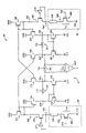
图3是本发明的读出放大器系统30的示意图。所述读出放大器系统包含于用于读取存储器(例如非易失性存储器)的电路结构中;明确地说,将单元电流与参考电流进行比较,以读取存储器单元的状态。本发明描述一种用于读出放大器的方案,其避免与现有技术实施方案的折叠级中的电容性电流分量有关的问题。所描述的晶体管是如图3的实例中所示的p沟道或n沟道。FIG. 3 is a schematic diagram of a
读出放大器系统30包含单元存储器阵列40和读出放大器电路42。单元存储器阵列40包含存储器单元500和参考单元600。存储器单元500存储预期由读出放大器电路42读取的信息。存储器单元500的漏极520通过位线530耦合到读出放大器电路42。类似地,参考单元600的漏极620通过位线630耦合到读出放大器电路。为了使单元500和600传导其电流,必须使栅极510和610以及漏极520和620的电压达到适宜的电压值。明确地说,漏极电压是由读出放大器电路42使用由反相器310和410构成的反馈配置来设置的。在替代实施例中,可使用其它方法来确保漏极电压的正确极化。晶体管300具有在节点540处耦合到位线530的源极,且反相器310耦合到晶体管300的栅极。类似地,晶体管400具有在节点640处耦合到位线630的源极,且反相器410耦合到晶体管400的栅极。反相器310和410确保适宜的电压值(例如,约1V)被设置于分别位于位线530和630的末端处的节点540和640上以及节点520和620上。The
晶体管100具有连接到晶体管300的漏极的漏极,且晶体管100的源极连接到Vdd。类似地,晶体管200具有连接到晶体管400的漏极的漏极,且晶体管200的源极连接到Vdd。在本文中,读出放大器电路42的“主电路”包含位于单元侧的组件(从晶体管100到晶体管300),以及位于参考侧的组件(从晶体管200到晶体管400)。
读出放大器电路42具有两个并联折叠级,其中所述级彼此类似。晶体管100和200用于向所述级提供电流。晶体管100与晶体管130和150成镜像配置,使得晶体管100的栅极连接到晶体管130和150的栅极。晶体管130是第一折叠级(或图3的配置实例中的“左边级”)的一部分,而晶体管150是第二折叠级(或图3的配置实例中的“右边级”)的一部分。类似地,晶体管200与晶体管230和250成镜像配置,使得晶体管200的栅极连接到晶体管230和250的栅极。晶体管230是第一级的一部分,而晶体管250是第二折叠级的一部分。单元电流由晶体管130和150转移到两个折叠级,而参考电流由晶体管230和250转移到两个折叠级。(左边级和右边级也可被视为整个单折叠级的部分)。The
在左边级中,晶体管130的漏极耦合到以二极管配置连接的晶体管140的漏极。晶体管140的栅极耦合到晶体管240的栅极,且晶体管240的漏极耦合到晶体管230的漏极。传递栅极720(具有选择线710)耦合在节点820与830之间,所述节点分别提供于晶体管130与140之间以及晶体管230与240之间。晶体管130和230的源极耦合到Vdd,而晶体管140和240的源极耦合到接地。In the left stage, the drain of
类似地,在电路的右边级中,晶体管250的漏极耦合到以二极管配置连接的晶体管260的漏极。晶体管260的栅极耦合到晶体管160的栅极,且晶体管160的漏极耦合到晶体管150的漏极。传递栅极730(具有选择线710)耦合在节点930与920之间,所述节点分别提供于晶体管150与160之间以及晶体管250与260之间。晶体管150和250的源极耦合到Vdd,而晶体管160和260的源极耦合到接地。Similarly, in the right stage of the circuit, the drain of
传递栅极700(具有选择线710)耦合在节点830与930之间。比较器1000使其输入端耦合于传递栅极700的任一侧上(即耦合于节点830和930处)。比较器1000的输出提供满幅信号,所述满幅信号用于提供呈“1”或“0”形式的数字信息。举例来说,传递栅极可包含由互补输入连接的互补晶体管对,例如,一个n沟道晶体管,其栅极作为启用信号710,且其漏极耦合到节点830且其源极耦合到节点930;以及一p沟道晶体管,其栅极作为启用信号710的互补信号,且其漏极耦合到节点830且其源极耦合到节点930。Transfer gate 700 (with select line 710 ) is coupled between
在替代实施例中,可在电路中使用其它类型的晶体管。举例来说,可使用PNP晶体管来代替PMOS,且使用NPN来代替NMOS。在其它实施例中,在对电路连接作适当修改的情况下,可将n沟道晶体管用于p沟道晶体管,且反之亦然。In alternative embodiments, other types of transistors may be used in the circuit. For example, PNP transistors may be used instead of PMOS, and NPNs instead of NMOS. In other embodiments, n-channel transistors may be used for p-channel transistors, and vice versa, with appropriate modifications to the circuit connections.
在图3中,将折叠方案加倍成两个并联级。电路的右边折叠级(晶体管150、160、250和260)等效于图2中所示的折叠级镜像配置。因此,所述折叠级的瞬变行为仍由等式(6)来描绘,且所述折叠级遭受针对图2的方案而描述的相同问题。当采用等式(6)并代入正确的电流和电容时,用于节点930的等式变为:In Figure 3, the folding scheme is doubled into two parallel stages. The right folding stage of the circuit (
假设节点920在瞬变周期期间放电,那么当从存储器单元500读取“0”状态时,图3的电路的右边级得益于杂散电流IC920。为了从存储器单元正确地读取“1”状态,电容性电流分量IC920应相对于差(Icell-Iref)来说为可忽略。Assuming
除来自主电路的连接被调换(即,提供于级的相对“侧”上)以外,电路的并联左边折叠级与右边级相同。举例来说,二极管连接式晶体管(左边级中的晶体管140)接收来自主电路的存储器单元侧的电流,而右边级中的二极管连接式晶体管260接收来自主电路的参考侧的电流。当代入正确的项时,可从等式(6)获得用于输出节点830的等式,从而产生以下等式:The parallel left fold stage of the circuit is identical to the right stage, except that the connections from the main circuit are reversed (ie, provided on opposite "sides" of the stage). For example, a diode-connected transistor (
类似于对图2中的电路的分析,可分析折叠电路的左边部分在其瞬变周期期间的行为。为了简单起见,仅在当电容性分量IC820为正时节点820正在放电的情况下提供此分析。当读取“1”状态(Icell>Iref)时,电流IC820与单元电流具有相同的符号,因此有助于使节点830放电,直到电流IC820相对于电流差(Iref-Icell)来说为不可忽略为止。最初,可使节点830放电;在放电后,节点830可由电流差(Iref-Icell)正确地充电。类似于对图2的电路的阐释,Vout信号符号在左边折叠级的瞬变行为开始时可能是不正确的,只有在电容性电流分量IC810小于电流差(Iref-Icell)时才变为正确。Similar to the analysis of the circuit in Figure 2, the behavior of the left part of the folded circuit during its transient period can be analyzed. For simplicity, this analysis is only provided when node 820 is discharging when
值得注意的是,折叠电路的两个并联级具有相反的行为:例如,左边级感测“1”而无任何问题,而右边级读取“0”而无问题。本发明的电路将两个折叠级合并在一起,以利用其相反行为。这样做时,整个电路的功能性从所述两个级获得最佳性能,从而抵消所述两个级的缺陷。通过检查用于Vout的等式来展示此结果:It is worth noting that the two parallel stages of the folded circuit have opposite behavior: for example, the left stage senses a "1" without any problem, while the right stage reads a "0" without problem. The circuit of the present invention combines the two folding stages to take advantage of their opposite behavior. In doing so, the functionality of the overall circuit derives its optimum performance from the two stages, thereby canceling out the imperfections of the two stages. Demonstrate this result by examining the equation for V out :
在此等式中,两个项IC820和IC920表示对读取操作的潜在干扰。如果两个项IC820和IC920以及两个寄生电容值C830和C930具有相同的值,那么两个杂散电流分量将自行抵消。因为两个电容性电流分量仅取决于与节点820和920耦合的寄生电容值,所以通过本发明的布局设计不难实现此目标。如果左边级与右边级中的晶体管具有相同(或大体上相同)的物理尺寸,且将电路布局实施为使得互连金属包含相同(或大体上相同)的寄生电容,那么两个杂散电流IC820和IC920的值将相同(或大体上相同),寄生电容C820和C920的值也将相同。当令C830=C930=Cout时,用于Vout的等式因此变为:In this equation, the two terms I C820 and I C920 represent the potential interference to the read operation. If the two terms I C820 and I C920 and the two parasitic capacitance values C 830 and C 930 have the same value, then the two stray current components will cancel themselves out. Since the two capacitive current components depend only on the parasitic capacitance coupling to
等式(10)展示仅单元侧电流和参考侧电流留下以确定Vout电压值和符号。因此,输出电压不再取决于折叠级中的二极管连接式晶体管的瞬变行为所产生的电容性电流。对于正确且准确的读取操作,不必等待此分量衰减到几乎为零。代替地,甚至在折叠级瞬变阶段期间,也有可能执行准确的读取操作。这与现有技术方案所需的时间相比,允许电路以非常快的方式执行读取操作。此外,由于所述电路结构,输出信号相对于先前方案而加倍。因此,相同电压差较早地出现在比较器输入处,其也允许比现有技术实施方案快的读取时间。Equation (10) shows that only the cell side current and the reference side current are left to determine the V out voltage value and sign. Therefore, the output voltage no longer depends on the capacitive current generated by the transient behavior of the diode-connected transistors in the folding stage. For a correct and accurate read operation, it is not necessary to wait for this component to decay to almost zero. Instead, it is possible to perform accurate read operations even during the folding stage transient phase. This allows the circuit to perform read operations in a very fast manner compared to the time required by prior art solutions. Furthermore, due to the described circuit structure, the output signal is doubled compared to previous solutions. Thus, the same voltage difference appears earlier at the comparator input, which also allows for a faster read time than prior art implementations.
通过甚至在瞬变/杂散电流尚不可忽略或尚不为零时抵消此电流对电路的效应,本发明允许甚至在瞬变电流和杂散电流对电路有影响的周期期间,快速且准确地读取存储器单元的状态。By canceling the effects of transient/spurious currents on the circuit even when such currents are not yet negligible or not zero, the invention allows fast and accurate Read the state of the memory cell.
尽管已根据所示的实施例而描述了本发明,但所属领域的技术人员将容易认识到,可存在所述实施例的变化,且那些变化将在本发明的精神和范围内。因此,所属领域的技术人员可在不脱离所附权利要求书的精神和范围的情况下,作出许多修改。While the invention has been described in terms of the illustrated embodiments, those skilled in the art will readily recognize that variations from the described embodiments can exist and those variations will fall within the spirit and scope of the invention. Accordingly, many modifications can be made by those skilled in the art without departing from the spirit and scope of the appended claims.
Claims (28)
Applications Claiming Priority (3)
| Application Number | Priority Date | Filing Date | Title |
|---|---|---|---|
| US11/652,770 | 2007-01-12 | ||
| US11/652,770 US7522463B2 (en) | 2007-01-12 | 2007-01-12 | Sense amplifier with stages to reduce capacitance mismatch in current mirror load |
| PCT/US2008/051025 WO2008089159A2 (en) | 2007-01-12 | 2008-01-15 | Sense amplifier with stages to reduce capacitance mismatch in current mirror load |
Publications (2)
| Publication Number | Publication Date |
|---|---|
| CN101681667A CN101681667A (en) | 2010-03-24 |
| CN101681667B true CN101681667B (en) | 2013-08-21 |
Family
ID=39617651
Family Applications (1)
| Application Number | Title | Priority Date | Filing Date |
|---|---|---|---|
| CN200880002070.3A Expired - Fee Related CN101681667B (en) | 2007-01-12 | 2008-01-15 | Sense amplifier with stages to reduce capacitance mismatch in current mirror load |
Country Status (5)
| Country | Link |
|---|---|
| US (1) | US7522463B2 (en) |
| CN (1) | CN101681667B (en) |
| DE (1) | DE112008000150T5 (en) |
| TW (1) | TWI349424B (en) |
| WO (1) | WO2008089159A2 (en) |
Families Citing this family (10)
| Publication number | Priority date | Publication date | Assignee | Title |
|---|---|---|---|---|
| US7724595B2 (en) * | 2008-01-08 | 2010-05-25 | Macronix International Co., Ltd. | Current-mode sense amplifier and sense amplifying method |
| JP5679801B2 (en) * | 2010-12-22 | 2015-03-04 | ラピスセミコンダクタ株式会社 | Nonvolatile memory device |
| US8514645B2 (en) | 2011-12-13 | 2013-08-20 | Atmel Corporation | Current-mode sense amplifier for high-speed sensing |
| JP5922935B2 (en) * | 2012-01-24 | 2016-05-24 | エスアイアイ・セミコンダクタ株式会社 | Read circuit of nonvolatile memory device |
| US9268899B2 (en) * | 2013-03-14 | 2016-02-23 | Silicon Storage Technology, Inc. | Transistor design for use in advanced nanometer flash memory devices |
| US9773537B2 (en) | 2015-10-27 | 2017-09-26 | Nxp Usa, Inc. | Sense path circuitry suitable for magnetic tunnel junction memories |
| US9659622B1 (en) | 2016-01-22 | 2017-05-23 | Nxp Usa, Inc. | Sense amplifier |
| US11271566B2 (en) * | 2018-12-14 | 2022-03-08 | Integrated Device Technology, Inc. | Digital logic compatible inputs in compound semiconductor circuits |
| US11862233B2 (en) | 2021-11-05 | 2024-01-02 | Changxin Memory Technologies, Inc. | System and method for detecting mismatch of sense amplifier |
| CN116092541B (en) * | 2021-11-05 | 2025-06-27 | 长鑫存储技术有限公司 | System and method for detecting mismatch of sense amplifier |
Citations (3)
| Publication number | Priority date | Publication date | Assignee | Title |
|---|---|---|---|---|
| CN1404067A (en) * | 2001-08-17 | 2003-03-19 | 株式会社东芝 | Semiconductor memory |
| JP2003178574A (en) * | 2001-10-11 | 2003-06-27 | Hewlett Packard Co <Hp> | High density memory sense amplifier |
| US7088626B2 (en) * | 2004-02-09 | 2006-08-08 | Sharp Kabushiki Kaisha | Bias voltage applying circuit and semiconductor memory device |
Family Cites Families (14)
| Publication number | Priority date | Publication date | Assignee | Title |
|---|---|---|---|---|
| US4713797A (en) | 1985-11-25 | 1987-12-15 | Motorola Inc. | Current mirror sense amplifier for a non-volatile memory |
| US4871933A (en) * | 1988-08-10 | 1989-10-03 | Actel Corporation | High-speed static differential sense amplifier |
| IT1308856B1 (en) * | 1999-10-29 | 2002-01-11 | St Microelectronics Srl | READING CIRCUIT FOR A NON-VOLATILE MEMORY. |
| DE10022263A1 (en) | 2000-05-08 | 2001-11-22 | Infineon Technologies Ag | Memory sense amplifier circuit, has precharging circuit and two amplifier stages that can be initialized to voltage supply and earth potentials respectively |
| DE10038383C1 (en) | 2000-08-07 | 2002-03-14 | Infineon Technologies Ag | High-speed sense current amplifier |
| US6747892B2 (en) | 2000-11-21 | 2004-06-08 | Sandisk Corporation | Sense amplifier for multilevel non-volatile integrated memory devices |
| US6535426B2 (en) | 2001-08-02 | 2003-03-18 | Stmicroelectronics, Inc. | Sense amplifier circuit and method for nonvolatile memory devices |
| EP1324344B1 (en) | 2001-12-28 | 2007-04-04 | STMicroelectronics S.r.l. | Sense amplifier structure for multilevel non-volatile memory devices and corresponding reading method |
| US6946882B2 (en) | 2002-12-20 | 2005-09-20 | Infineon Technologies Ag | Current sense amplifier |
| US7251178B2 (en) | 2004-09-07 | 2007-07-31 | Infineon Technologies Ag | Current sense amplifier |
| ITRM20040199A1 (en) | 2004-04-21 | 2004-07-21 | Micron Technology Inc | DETECTION AMPLIFIER FOR A NON-VOLATILE MEMORY DEVICE. |
| ITMI20042074A1 (en) | 2004-10-29 | 2005-01-29 | St Microelectronics Srl | CURRENT READING AMPLIFIER FOR LOW VOLTAGE APPLICATIONS WITH DIRECT SENSING ON THE BITLINE OF A MEMORY MATRIX |
| US7161861B2 (en) | 2004-11-15 | 2007-01-09 | Infineon Technologies Ag | Sense amplifier bitline boost circuit |
| US20060146624A1 (en) | 2004-12-02 | 2006-07-06 | Saifun Semiconductors, Ltd. | Current folding sense amplifier |
-
2007
- 2007-01-12 US US11/652,770 patent/US7522463B2/en active Active
-
2008
- 2008-01-11 TW TW097101304A patent/TWI349424B/en not_active IP Right Cessation
- 2008-01-15 CN CN200880002070.3A patent/CN101681667B/en not_active Expired - Fee Related
- 2008-01-15 WO PCT/US2008/051025 patent/WO2008089159A2/en not_active Ceased
- 2008-01-15 DE DE112008000150T patent/DE112008000150T5/en not_active Withdrawn
Patent Citations (3)
| Publication number | Priority date | Publication date | Assignee | Title |
|---|---|---|---|---|
| CN1404067A (en) * | 2001-08-17 | 2003-03-19 | 株式会社东芝 | Semiconductor memory |
| JP2003178574A (en) * | 2001-10-11 | 2003-06-27 | Hewlett Packard Co <Hp> | High density memory sense amplifier |
| US7088626B2 (en) * | 2004-02-09 | 2006-08-08 | Sharp Kabushiki Kaisha | Bias voltage applying circuit and semiconductor memory device |
Non-Patent Citations (2)
| Title |
|---|
| JP特开2003-178574A 2003.06.27 |
| US 7,088,626 B2,2006.08.08,说明书第10栏第20行至第19栏第10行,图1-3,11,12. |
Also Published As
| Publication number | Publication date |
|---|---|
| US20080170454A1 (en) | 2008-07-17 |
| WO2008089159A2 (en) | 2008-07-24 |
| TWI349424B (en) | 2011-09-21 |
| CN101681667A (en) | 2010-03-24 |
| DE112008000150T5 (en) | 2009-12-03 |
| US7522463B2 (en) | 2009-04-21 |
| WO2008089159A3 (en) | 2009-12-30 |
| TW200838124A (en) | 2008-09-16 |
Similar Documents
| Publication | Publication Date | Title |
|---|---|---|
| CN101681667B (en) | Sense amplifier with stages to reduce capacitance mismatch in current mirror load | |
| US7545694B2 (en) | Sense amplifier with leakage testing and read debug capability | |
| US9105331B2 (en) | Semiconductor memory apparatus and method of operating using the same | |
| US7483306B2 (en) | Fast and accurate sensing amplifier for low voltage semiconductor memory | |
| US9589630B2 (en) | Low voltage current reference generator for a sensing amplifier | |
| EP1493158B1 (en) | Single-ended current sense amplifier | |
| CN113607293B (en) | Integrated circuit with temperature sensor | |
| KR102524472B1 (en) | Reference voltage generating circuit | |
| US7482843B2 (en) | Signal amplifier | |
| US20160380596A1 (en) | Sense Amplifier | |
| JPH10188585A (en) | Nonvolatile semiconductor memory device and its constant voltage generating circuit | |
| US6836443B2 (en) | Apparatus and method of high speed current sensing for low voltage operation | |
| ITMI992119A1 (en) | HIGH READING MEMORY CIRCUIT FOR CURRENT LEVEL DISCRIMINATION CAPACITY | |
| KR100955089B1 (en) | Cascode Amplifier Circuit to Generate Fast, Stable, and Accurate Bitline Voltages | |
| KR100267012B1 (en) | Sense amplifier of semiconductor memory device | |
| US6707703B2 (en) | Negative voltage generating circuit | |
| JPH10125084A (en) | Current amplifier | |
| JP2002025286A (en) | Semiconductor memory integrated circuit | |
| US7268589B2 (en) | Address transition detector for fast flash memory device | |
| US8077499B2 (en) | Semiconductor integrated memory circuit and trimming method thereof | |
| JP2007234206A (en) | Semiconductor memory device, power supply detector, semiconductor device | |
| KR100357041B1 (en) | Low Voltage Current Sensing Amplifier | |
| KR100721545B1 (en) | Pulse Width Mismatch Detector | |
| JP2008090885A (en) | Semiconductor integrated device | |
| US20160300598A1 (en) | Circuit |
Legal Events
| Date | Code | Title | Description |
|---|---|---|---|
| C06 | Publication | ||
| PB01 | Publication | ||
| C10 | Entry into substantive examination | ||
| SE01 | Entry into force of request for substantive examination | ||
| C14 | Grant of patent or utility model | ||
| GR01 | Patent grant | ||
| C17 | Cessation of patent right | ||
| CF01 | Termination of patent right due to non-payment of annual fee |
Granted publication date: 20130821 Termination date: 20140115 |