[go: up one dir, main page]

CN101542745B - Multi-junction solar cells and methods and apparatuses for forming the same - Google Patents

Multi-junction solar cells and methods and apparatuses for forming the same Download PDF

Info

Publication number
CN101542745B
CN101542745B CN2008800001789A CN200880000178A CN101542745B CN 101542745 B CN101542745 B CN 101542745B CN 2008800001789 A CN2008800001789 A CN 2008800001789A CN 200880000178 A CN200880000178 A CN 200880000178A CN 101542745 B CN101542745 B CN 101542745B
Authority
CN
China
Prior art keywords
silicon layer
amorphous silicon
layer
type
hydrogen
Prior art date
Legal status (The legal status is an assumption and is not a legal conclusion. Google has not performed a legal analysis and makes no representation as to the accuracy of the status listed.)
Expired - Fee Related
Application number
CN2008800001789A
Other languages
Chinese (zh)
Other versions
CN101542745A (en
Inventor
盛殊然
蔡容基
崔寿永
元泰景
李立伟
Current Assignee (The listed assignees may be inaccurate. Google has not performed a legal analysis and makes no representation or warranty as to the accuracy of the list.)
Applied Materials Inc
Original Assignee
Applied Materials Inc
Priority date (The priority date is an assumption and is not a legal conclusion. Google has not performed a legal analysis and makes no representation as to the accuracy of the date listed.)
Filing date
Publication date
Priority claimed from US12/110,120 external-priority patent/US20080223440A1/en
Application filed by Applied Materials Inc filed Critical Applied Materials Inc
Publication of CN101542745A publication Critical patent/CN101542745A/en
Application granted granted Critical
Publication of CN101542745B publication Critical patent/CN101542745B/en
Expired - Fee Related legal-status Critical Current
Anticipated expiration legal-status Critical

Links

Images

Classifications

    • HELECTRICITY
    • H10SEMICONDUCTOR DEVICES; ELECTRIC SOLID-STATE DEVICES NOT OTHERWISE PROVIDED FOR
    • H10FINORGANIC SEMICONDUCTOR DEVICES SENSITIVE TO INFRARED RADIATION, LIGHT, ELECTROMAGNETIC RADIATION OF SHORTER WAVELENGTH OR CORPUSCULAR RADIATION
    • H10F77/00Constructional details of devices covered by this subclass
    • H10F77/10Semiconductor bodies
    • H10F77/16Material structures, e.g. crystalline structures, film structures or crystal plane orientations
    • H10F77/169Thin semiconductor films on metallic or insulating substrates
    • H10F77/1692Thin semiconductor films on metallic or insulating substrates the films including only Group IV materials
    • HELECTRICITY
    • H10SEMICONDUCTOR DEVICES; ELECTRIC SOLID-STATE DEVICES NOT OTHERWISE PROVIDED FOR
    • H10FINORGANIC SEMICONDUCTOR DEVICES SENSITIVE TO INFRARED RADIATION, LIGHT, ELECTROMAGNETIC RADIATION OF SHORTER WAVELENGTH OR CORPUSCULAR RADIATION
    • H10F19/00Integrated devices, or assemblies of multiple devices, comprising at least one photovoltaic cell covered by group H10F10/00, e.g. photovoltaic modules
    • H10F19/10Integrated devices, or assemblies of multiple devices, comprising at least one photovoltaic cell covered by group H10F10/00, e.g. photovoltaic modules comprising photovoltaic cells in arrays in a single semiconductor substrate, the photovoltaic cells having vertical junctions or V-groove junctions
    • HELECTRICITY
    • H10SEMICONDUCTOR DEVICES; ELECTRIC SOLID-STATE DEVICES NOT OTHERWISE PROVIDED FOR
    • H10FINORGANIC SEMICONDUCTOR DEVICES SENSITIVE TO INFRARED RADIATION, LIGHT, ELECTROMAGNETIC RADIATION OF SHORTER WAVELENGTH OR CORPUSCULAR RADIATION
    • H10F10/00Individual photovoltaic cells, e.g. solar cells
    • H10F10/10Individual photovoltaic cells, e.g. solar cells having potential barriers
    • H10F10/17Photovoltaic cells having only PIN junction potential barriers
    • H10F10/172Photovoltaic cells having only PIN junction potential barriers comprising multiple PIN junctions, e.g. tandem cells
    • HELECTRICITY
    • H10SEMICONDUCTOR DEVICES; ELECTRIC SOLID-STATE DEVICES NOT OTHERWISE PROVIDED FOR
    • H10FINORGANIC SEMICONDUCTOR DEVICES SENSITIVE TO INFRARED RADIATION, LIGHT, ELECTROMAGNETIC RADIATION OF SHORTER WAVELENGTH OR CORPUSCULAR RADIATION
    • H10F19/00Integrated devices, or assemblies of multiple devices, comprising at least one photovoltaic cell covered by group H10F10/00, e.g. photovoltaic modules
    • H10F19/30Integrated devices, or assemblies of multiple devices, comprising at least one photovoltaic cell covered by group H10F10/00, e.g. photovoltaic modules comprising thin-film photovoltaic cells
    • HELECTRICITY
    • H10SEMICONDUCTOR DEVICES; ELECTRIC SOLID-STATE DEVICES NOT OTHERWISE PROVIDED FOR
    • H10FINORGANIC SEMICONDUCTOR DEVICES SENSITIVE TO INFRARED RADIATION, LIGHT, ELECTROMAGNETIC RADIATION OF SHORTER WAVELENGTH OR CORPUSCULAR RADIATION
    • H10F71/00Manufacture or treatment of devices covered by this subclass
    • H10F71/10Manufacture or treatment of devices covered by this subclass the devices comprising amorphous semiconductor material
    • H10F71/103Manufacture or treatment of devices covered by this subclass the devices comprising amorphous semiconductor material including only Group IV materials
    • HELECTRICITY
    • H10SEMICONDUCTOR DEVICES; ELECTRIC SOLID-STATE DEVICES NOT OTHERWISE PROVIDED FOR
    • H10FINORGANIC SEMICONDUCTOR DEVICES SENSITIVE TO INFRARED RADIATION, LIGHT, ELECTROMAGNETIC RADIATION OF SHORTER WAVELENGTH OR CORPUSCULAR RADIATION
    • H10F71/00Manufacture or treatment of devices covered by this subclass
    • H10F71/121The active layers comprising only Group IV materials
    • H10F71/1224The active layers comprising only Group IV materials comprising microcrystalline silicon
    • YGENERAL TAGGING OF NEW TECHNOLOGICAL DEVELOPMENTS; GENERAL TAGGING OF CROSS-SECTIONAL TECHNOLOGIES SPANNING OVER SEVERAL SECTIONS OF THE IPC; TECHNICAL SUBJECTS COVERED BY FORMER USPC CROSS-REFERENCE ART COLLECTIONS [XRACs] AND DIGESTS
    • Y02TECHNOLOGIES OR APPLICATIONS FOR MITIGATION OR ADAPTATION AGAINST CLIMATE CHANGE
    • Y02EREDUCTION OF GREENHOUSE GAS [GHG] EMISSIONS, RELATED TO ENERGY GENERATION, TRANSMISSION OR DISTRIBUTION
    • Y02E10/00Energy generation through renewable energy sources
    • Y02E10/50Photovoltaic [PV] energy
    • Y02E10/545Microcrystalline silicon PV cells
    • YGENERAL TAGGING OF NEW TECHNOLOGICAL DEVELOPMENTS; GENERAL TAGGING OF CROSS-SECTIONAL TECHNOLOGIES SPANNING OVER SEVERAL SECTIONS OF THE IPC; TECHNICAL SUBJECTS COVERED BY FORMER USPC CROSS-REFERENCE ART COLLECTIONS [XRACs] AND DIGESTS
    • Y02TECHNOLOGIES OR APPLICATIONS FOR MITIGATION OR ADAPTATION AGAINST CLIMATE CHANGE
    • Y02EREDUCTION OF GREENHOUSE GAS [GHG] EMISSIONS, RELATED TO ENERGY GENERATION, TRANSMISSION OR DISTRIBUTION
    • Y02E10/00Energy generation through renewable energy sources
    • Y02E10/50Photovoltaic [PV] energy
    • Y02E10/548Amorphous silicon PV cells
    • YGENERAL TAGGING OF NEW TECHNOLOGICAL DEVELOPMENTS; GENERAL TAGGING OF CROSS-SECTIONAL TECHNOLOGIES SPANNING OVER SEVERAL SECTIONS OF THE IPC; TECHNICAL SUBJECTS COVERED BY FORMER USPC CROSS-REFERENCE ART COLLECTIONS [XRACs] AND DIGESTS
    • Y02TECHNOLOGIES OR APPLICATIONS FOR MITIGATION OR ADAPTATION AGAINST CLIMATE CHANGE
    • Y02PCLIMATE CHANGE MITIGATION TECHNOLOGIES IN THE PRODUCTION OR PROCESSING OF GOODS
    • Y02P70/00Climate change mitigation technologies in the production process for final industrial or consumer products
    • Y02P70/50Manufacturing or production processes characterised by the final manufactured product

Landscapes

  • Photovoltaic Devices (AREA)

Abstract

Embodiments of the present invention generally relate to solar cells and methods and apparatuses for forming the same. More particularly, embodiments of the present invention relate to thin film multi-junction solar cells and methods and apparatuses for forming the same. Embodiments of the present invention also include an improved thin film silicon solar cell, and methods and apparatus for forming the same, where one or more of the layers in the solar cell comprises at least one amorphous silicon layer that has improved electrical characteristics and mechanical properties, and is capable of being deposited at rates many times faster than conventional amorphous silicon deposition processes.

Description

多结太阳能电池及其形成方法与设备Multi-junction solar cell and its forming method and device

技术领域 technical field

本发明实施例一般涉及太阳能电池及其形成方法和设备。更具体地,本发明实施例涉及薄膜多结太阳能电池及其形成方法和设备。Embodiments of the invention generally relate to solar cells and methods and apparatus for forming the same. More specifically, embodiments of the present invention relate to thin film multi-junction solar cells and methods and devices for forming the same.

背景技术 Background technique

太阳能电池将太阳辐射与其它光线转换成可用的电能。因为光伏(photovoltaic)效应而发生能量转换。太阳能电池可由晶态材料或由非晶或微晶材料所形成。一般而言,现今大量生产的太阳能电池主要类型有两种,分别为结晶硅太阳能电池与薄膜太阳能电池。结晶硅太阳能电池通常应用单结晶基材(即,纯硅的单晶基材)或多结晶硅基材(即,多晶或多晶硅)。在硅基材上沉积附加膜层以改善光线俘获、形成电路以及保护器件。薄膜太阳能电池使用沉积在适合基材上的材料薄层,以形成一个或多个p-n结。适合的基材包括玻璃、金属和聚合物基材。已经发现,薄膜太阳能电池的性能在暴露于光线后会随着时间而降低,这会导致器件稳定性不如预期。通常会降低的太阳能电池性能为填充因数(FF)、短路电流与开路电压(Voc)。Solar cells convert solar radiation and other light into usable electrical energy. Energy conversion occurs due to the photovoltaic effect. Solar cells can be formed from crystalline materials or from amorphous or microcrystalline materials. Generally speaking, there are two main types of solar cells mass-produced today, namely crystalline silicon solar cells and thin-film solar cells. Crystalline silicon solar cells typically employ either a single crystalline substrate (ie, a single crystal substrate of pure silicon) or a polycrystalline silicon substrate (ie, polycrystalline or polycrystalline silicon). Additional layers are deposited on silicon substrates to improve light trapping, form circuits, and protect devices. Thin film solar cells use thin layers of material deposited on a suitable substrate to form one or more p-n junctions. Suitable substrates include glass, metal and polymeric substrates. It has been found that the performance of thin-film solar cells degrades over time after exposure to light, which can lead to less-than-expected device stability. Solar cell properties that typically degrade are fill factor (FF), short circuit current and open circuit voltage (Voc).

目前薄膜太阳能电池的问题包括低效率与高成本。因此,需要改良的薄膜太阳能电池及在工厂环境中制造改良的薄膜太阳能电池的方法与设备。还需要可制造具有高填充因数、高短路电流、高开路电压与良好器件稳定性的高稳定性p-i-n太阳能电池的工艺。Problems with current thin-film solar cells include low efficiency and high cost. Accordingly, there is a need for improved thin film solar cells and methods and apparatus for manufacturing improved thin film solar cells in a factory environment. There is also a need for a process that can fabricate highly stable p-i-n solar cells with high fill factor, high short circuit current, high open circuit voltage and good device stability.

发明内容 Contents of the invention

本发明的实施例涉及薄膜多结太阳能电池及其形成方法与设备。在一实施例中,在基材上形成薄膜多结太阳能电池的方法包括形成第一p-i-n结并于第一p-i-n结上形成第二p-i-n结。形成第一p-i-n结可包括形成p型非晶硅层、在p型非晶硅层上形成本征型(intrinsic type)非晶硅层、并在本征型非晶硅层上形成n型微晶硅层。形成第二p-i-n结可包括形成p型微晶硅层、在p型微晶硅层上形成本征型微晶硅层、并在本征型微晶层上形成n型非晶硅层。在一实施例中,形成薄膜多结太阳能电池的设备包括至少一个配置成形成第一p-i-n结的第一系统与至少一个配置成在第一p-i-n结上形成第二p-i-n结的第二系统。第一系统可包括配置成沉积p型非晶硅层的单一p-腔室与数个各自配置成沉积本征型非晶硅层与n型微晶硅层的i/n-腔室。第二系统可包括配置成沉积p型微晶硅层的单一p-腔室与数个各自配置成沉积本征型微晶硅层与n型非晶硅层的i/n-腔室。Embodiments of the invention relate to thin film multi-junction solar cells and methods and devices for forming the same. In one embodiment, a method of forming a thin film multi-junction solar cell on a substrate includes forming a first p-i-n junction and forming a second p-i-n junction on the first p-i-n junction. Forming the first p-i-n junction may include forming a p-type amorphous silicon layer, forming an intrinsic type (intrinsic type) amorphous silicon layer on the p-type amorphous silicon layer, and forming an n-type microcrystalline silicon layer on the intrinsic type amorphous silicon layer. crystalline silicon layer. Forming the second p-i-n junction may include forming a p-type microcrystalline silicon layer, forming an intrinsic type microcrystalline silicon layer on the p-type microcrystalline silicon layer, and forming an n-type amorphous silicon layer on the intrinsic type microcrystalline silicon layer. In one embodiment, an apparatus for forming a thin film multi-junction solar cell includes at least one first system configured to form a first p-i-n junction and at least one second system configured to form a second p-i-n junction on the first p-i-n junction. The first system may include a single p-chamber configured to deposit a p-type amorphous silicon layer and a plurality of i/n-chambers each configured to deposit an intrinsic type amorphous silicon layer and an n-type microcrystalline silicon layer. The second system may include a single p-chamber configured to deposit a p-type microcrystalline silicon layer and a plurality of i/n-chambers each configured to deposit an intrinsic type microcrystalline silicon layer and an n-type amorphous silicon layer.

本发明实施例还包括提供一种在基材上形成薄膜多结太阳能电池的方法,该方法包括在基材上形成第一光伏结并在第一光伏结上形成第二光伏结,形成第二光伏结包括形成p型微晶硅层、在p型微晶硅层上形成本征型微晶硅层、并在本征型微晶层上形成n型非晶硅层,其中当本征型微晶硅层形成时,一个或更多个处理变量被调整以控制本征型微晶硅层厚度内二个或更多个点处的结晶系数(crystalline fraction)。Embodiments of the present invention also include providing a method for forming a thin film multi-junction solar cell on a substrate, the method comprising forming a first photovoltaic junction on the substrate and forming a second photovoltaic junction on the first photovoltaic junction, forming a second photovoltaic junction The photovoltaic junction includes forming a p-type microcrystalline silicon layer, forming an intrinsic type microcrystalline silicon layer on the p-type microcrystalline silicon layer, and forming an n-type amorphous silicon layer on the intrinsic type microcrystalline layer, wherein when the intrinsic type As the microcrystalline silicon layer is formed, one or more process variables are adjusted to control the crystalline fraction at two or more points within the thickness of the intrinsic microcrystalline silicon layer.

本发明实施例还提供一种在基材上形成薄膜多结太阳能电池的方法,该方法包括:在基材上形成第一光伏结,在基材上形成第一光伏结包括形成p型非晶硅层、在p型非晶硅层上形成本征型非晶硅层、并在本征型非晶硅层上形成n型微晶硅层,其中本征型非晶硅层包括p-i缓冲本征型非晶硅层与主体(bulk)本征型非晶硅层;以及在第一光伏结上形成第二光伏结,在第一光伏结上形成第二光伏结包括形成p型微晶硅层、在p型微晶硅层上形成本征型微晶硅层、并在本征型微晶层上形成n型非晶硅层。An embodiment of the present invention also provides a method for forming a thin film multi-junction solar cell on a substrate, the method comprising: forming a first photovoltaic junction on the substrate, and forming the first photovoltaic junction on the substrate includes forming a p-type amorphous Silicon layer, forming an intrinsic type amorphous silicon layer on the p-type amorphous silicon layer, and forming an n-type microcrystalline silicon layer on the intrinsic type amorphous silicon layer, wherein the intrinsic type amorphous silicon layer includes a p-i buffer An intrinsic type amorphous silicon layer and a bulk intrinsic type amorphous silicon layer; and forming a second photovoltaic junction on the first photovoltaic junction, and forming the second photovoltaic junction on the first photovoltaic junction includes forming p-type microcrystalline silicon layer, forming an intrinsic type microcrystalline silicon layer on the p-type microcrystalline silicon layer, and forming an n-type amorphous silicon layer on the intrinsic type microcrystalline silicon layer.

本发明实施例还包括提供一种串接(tandem)结光伏器件,该串接结光伏器件包括第一光伏结与第二光伏结,其中第二光伏结包括p型掺杂微晶硅层、本征型微晶硅层、与邻接本征型微晶硅层的n型掺杂非晶硅层,其中本征型微晶硅层通过多步骤沉积处理加以形成,其中每个沉积步骤具有不同氢/硅烷比例的气体混合物,以在每个沉积步骤中形成不同的薄膜结晶系数。在一实施例中,不同的氢/硅烷比例控制跨本征型微晶硅层的整个厚度均匀地形成的结晶系数。Embodiments of the present invention also provide a tandem junction photovoltaic device, the tandem junction photovoltaic device includes a first photovoltaic junction and a second photovoltaic junction, wherein the second photovoltaic junction includes a p-type doped microcrystalline silicon layer, An intrinsic type microcrystalline silicon layer, and an n-type doped amorphous silicon layer adjacent to the intrinsic type microcrystalline silicon layer, wherein the intrinsic type microcrystalline silicon layer is formed by a multi-step deposition process, wherein each deposition step has a different Gas mixtures with hydrogen/silane ratios to form different film crystallization coefficients in each deposition step. In one embodiment, different hydrogen/silane ratios control the crystallization coefficient that forms uniformly across the entire thickness of the intrinsic type microcrystalline silicon layer.

附图说明 Description of drawings

因此,可详细理解本发明的上述陈述特征的方式,即对以上简述发明的更具体描述可通过参考实施例得到,一些实施例在附图中描述。So that the manner in which the above recited features of the invention can be understood in detail, a more particular description of the invention briefly described above can be had by reference to the Examples, some of which are illustrated in the accompanying drawings.

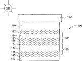
图1是朝向光线或太阳辐射的多结太阳能电池的某些实施例的示意图。Figure 1 is a schematic diagram of certain embodiments of multi-junction solar cells oriented towards light or solar radiation.

图2是图1的多结太阳能电池进一步包括n型非晶硅缓冲层的示意图。FIG. 2 is a schematic diagram of the multi-junction solar cell of FIG. 1 further comprising an n-type amorphous silicon buffer layer.

图3是图1的多结太阳能电池进一步包括p型微晶硅接触层的示意图。FIG. 3 is a schematic diagram of the multi-junction solar cell of FIG. 1 further comprising a p-type microcrystalline silicon contact layer.

图4是可沉积一个或多个太阳能电池膜的等离子体辅助化学气相沉积(PECVD)室的一实施例的示意截面图。4 is a schematic cross-sectional view of one embodiment of a plasma-assisted chemical vapor deposition (PECVD) chamber that can deposit one or more solar cell films.

图5是具有数个处理室的处理系统的一实施例的示意俯视图。Figure 5 is a schematic top view of an embodiment of a processing system having several processing chambers.

图6描述了用以形成串接p-i-n结太阳能电池的沉积参数设定。Figure 6 depicts the deposition parameter settings for forming tandem p-i-n junction solar cells.

图7描述了本发明一实施例的太阳能电池的特性。FIG. 7 depicts the characteristics of a solar cell according to an embodiment of the present invention.

图8A-C描述单结太阳能电池的不同实施例的示意图。8A-C depict schematic diagrams of different embodiments of single junction solar cells.

图9描述单结太阳能电池的不同实施例的示意图。Figure 9 depicts schematic diagrams of different embodiments of single junction solar cells.

图10是根据本发明一实施例的单结太阳能电池的示意图。FIG. 10 is a schematic diagram of a single-junction solar cell according to an embodiment of the present invention.

然而,值得注意的是附图仅描述本发明的典型实施例,因此并不视为对本发明范围的限制,因为本发明允许其它等效实施例。It is to be noted, however, that the appended drawings depict only typical embodiments of this invention and are therefore not to be considered limiting of its scope, for the invention may admit to other equally effective embodiments.

为了有助于理解,尽可能使用相同的附图标记来表示附图中相同的元件。To facilitate understanding, identical reference numerals have been used wherever possible to refer to identical elements in the drawings.

具体实施方式 Detailed ways

本发明实施例包括改良的薄膜多结太阳能电池及其形成方法和设备。图1是朝向光或太阳辐射101的多结太阳能电池100的某些实施例的示意图。太阳能电池100包括基材102,诸如玻璃基材、聚合物基材、金属基材或其它适当基材,基材102形成有薄膜。太阳能电池100进一步包括形成在基材102上的第一透明导电氧化物(TCO)层110、形成在第一TCO层110上的第一p-i-n结120、形成在第一p-i-n结120上的第二p-i-n结130、形成在第二p-i-n结130上的第二TCO层140以及形成在第二TCO层140上的金属基底层150。为了通过增强光俘获来改善光吸收,通过湿法、等离子体、离子和/或机械处理,可任选地使基材和/或一个或多个形成在基材上的薄膜具有纹理。例如,在图1中所示的实施例中,使第一TCO层110具有纹理,随后沉积于第一TCO层110上的薄膜通常会跟随下方表面的形貌起伏。Embodiments of the invention include improved thin film multi-junction solar cells and methods and apparatus for forming the same. FIG. 1 is a schematic diagram of certain embodiments of a multi-junction solar cell 100 oriented toward light or solar radiation 101 . Solar cell 100 includes a substrate 102, such as a glass substrate, a polymer substrate, a metal substrate, or other suitable substrate, formed with a thin film. The solar cell 100 further includes a first transparent conductive oxide (TCO) layer 110 formed on the substrate 102, a first p-i-n junction 120 formed on the first TCO layer 110, a second p-i-n junction formed on the first p-i-n junction 120 The p-i-n junction 130 , the second TCO layer 140 formed on the second p-i-n junction 130 , and the metal base layer 150 formed on the second TCO layer 140 . To improve light absorption by enhancing light trapping, the substrate and/or one or more films formed on the substrate may optionally be textured by wet, plasma, ionic, and/or mechanical treatments. For example, in the embodiment shown in FIG. 1 , the first TCO layer 110 is textured, and then the thin film deposited on the first TCO layer 110 generally follows the topography of the underlying surface.

第一TCO层110和第二TCO层140各自包括氧化锡、氧化锌、氧化铟锡、锡酸镉、上述的组合物或其它适合的材料。可以理解TCO材料还可包括附加的掺杂物和成分。例如,氧化锌可进一步包括掺杂物,诸如铝、镓、硼和其它适当掺杂物。氧化锌较佳地包括5原子%或更少的掺杂物,并且更佳为包括2.5原子%或更少的铝。在某些情况中,可由玻璃制造商提供已经设置有第一TCO层110的基材102。The first TCO layer 110 and the second TCO layer 140 each include tin oxide, zinc oxide, indium tin oxide, cadmium stannate, combinations thereof, or other suitable materials. It is understood that the TCO material may also include additional dopants and components. For example, zinc oxide may further include dopants such as aluminum, gallium, boron, and other suitable dopants. Zinc oxide preferably includes 5 atomic % or less of dopants, and more preferably includes 2.5 atomic % or less of aluminum. In some cases, the substrate 102 may already be provided with the first TCO layer 110 by a glass manufacturer.

第一p-i-n结120可包括p型非晶硅层122、形成在p型非晶硅层122上的本征型非晶硅层124以及形成在本征型非晶硅层124上的n型微晶硅层126。在某些实施例中,p型非晶硅层122可形成的厚度在约

Figure GSB00000766977000041
和约
Figure GSB00000766977000042
之间。在某些实施例中,本征型非晶硅层124可形成的厚度在约
Figure GSB00000766977000043
和约
Figure GSB00000766977000044
之间。在某些实施例中,n型微晶半导体层126可形成的厚度在约
Figure GSB00000766977000045
和约
Figure GSB00000766977000046
之间。The first pin junction 120 may include a p-type amorphous silicon layer 122, an intrinsic type amorphous silicon layer 124 formed on the p-type amorphous silicon layer 122, and an n-type microstructure formed on the intrinsic type amorphous silicon layer 124. crystalline silicon layer 126 . In some embodiments, the p-type amorphous silicon layer 122 can be formed with a thickness of about
Figure GSB00000766977000041
peace treaty
Figure GSB00000766977000042
between. In some embodiments, the intrinsic type amorphous silicon layer 124 can be formed with a thickness of about
Figure GSB00000766977000043
peace treaty
Figure GSB00000766977000044
between. In some embodiments, the n-type microcrystalline semiconductor layer 126 can be formed to a thickness of about
Figure GSB00000766977000045
peace treaty
Figure GSB00000766977000046
between.

第二p-i-n结130可包括p型微晶硅层132、形成在p型微晶硅层132上的本征型微晶硅层134以及形成在本征型微晶硅层134上的n型非晶硅层136。在某些实施例中,p型微晶硅层132可形成的厚度在约和约

Figure GSB00000766977000048
之间。在某些实施例中,本征型微晶硅层134可形成的厚度在约
Figure GSB00000766977000049
和约
Figure GSB000007669770000410
之间。在某些实施例中,n型非晶硅层136可形成的厚度在约
Figure GSB000007669770000411
和约
Figure GSB000007669770000412
之间。The second pin junction 130 may include a p-type microcrystalline silicon layer 132, an intrinsic type microcrystalline silicon layer 134 formed on the p-type microcrystalline silicon layer 132, and an n-type non-crystalline silicon layer formed on the intrinsic type microcrystalline silicon layer 134. Crystalline silicon layer 136 . In some embodiments, the p-type microcrystalline silicon layer 132 can be formed with a thickness of about peace treaty
Figure GSB00000766977000048
between. In some embodiments, the intrinsic microcrystalline silicon layer 134 can be formed to a thickness of about
Figure GSB00000766977000049
peace treaty
Figure GSB000007669770000410
between. In some embodiments, the n-type amorphous silicon layer 136 can be formed to a thickness of about
Figure GSB000007669770000411
peace treaty
Figure GSB000007669770000412
between.

金属基底层150可包括但不限于选自Al、Ag、Ti、Cr、Au、Cu、Pt、上述的合金或上述的组合物所构成的群组的材料。可执行例如激光刻划处理的其它处理以形成太阳能电池100。可在金属基底层150上设置其它膜、材料、基材和/或封装以完成太阳能电池。可使太阳能电池相互连接以形成模块,接着可连接模块以形成阵列。The metal base layer 150 may include, but is not limited to, a material selected from the group consisting of Al, Ag, Ti, Cr, Au, Cu, Pt, the above alloys, or the above combinations. Other processing, such as a laser scribing process, may be performed to form solar cell 100 . Other films, materials, substrates, and/or encapsulation may be disposed on the metal base layer 150 to complete the solar cell. The solar cells can be connected to each other to form a module, and the modules can then be connected to form an array.

太阳辐射101通过p-i-n结120、130的本征层吸收,并转换成电子空穴对。延伸穿过本征层且在p型层和n型层之间产生的电场,可使电子流向n型层并使空穴流向p型层,因而产生电流。因为非晶硅和微晶硅吸收不同波长的太阳辐射101,所以第一p-i-n结120包括本征型非晶硅层124而第二p-i-n结130包括本征型微晶硅层134。因此,太阳能电池100由于俘获较大部分的太阳辐射光谱而更具效率。由于非晶硅与微晶硅相比具有较宽的能带隙,因此非晶硅本征层和微晶本征层以使得太阳辐射101首先通过本征型非晶硅层124,然后通过本征型微晶硅层134的方式堆叠。不被第一p-i-n结120吸收的太阳辐射继续入射到第二p-i-n结130上。令人惊讶地发现,此处公开为太阳能电池设置的第一p-i-n结120以及第二p-i-n结130的p-i-n层的厚度可改进效率并且降低制造成本。除了明确地在权利要求中陈述之外,不希望为理论所限制,一般认为:一方面,较厚的本征层124、134有利于吸收更多量的太阳辐射光谱,另一方面,若本征层124、134和/或p-i-n结120、130太厚,则从那里穿过的电子流会受阻碍。Solar radiation 101 is absorbed by the intrinsic layers of the p-i-n junctions 120, 130 and converted into electron-hole pairs. An electric field extending across the intrinsic layer and created between the p-type layer and the n-type layer causes electrons to flow to the n-type layer and holes to flow to the p-type layer, thereby generating an electric current. Because amorphous silicon and microcrystalline silicon absorb different wavelengths of solar radiation 101 , the first p-i-n junction 120 includes an intrinsic type amorphous silicon layer 124 and the second p-i-n junction 130 includes an intrinsic type microcrystalline silicon layer 134 . Thus, solar cell 100 is more efficient by capturing a larger portion of the solar radiation spectrum. Since amorphous silicon has a wider energy band gap than microcrystalline silicon, the intrinsic layer of amorphous silicon and the intrinsic layer of microcrystalline make the solar radiation 101 first pass through the intrinsic type amorphous silicon layer 124, and then pass through the intrinsic type amorphous silicon layer 124. The typical microcrystalline silicon layer 134 is stacked. Solar radiation not absorbed by the first p-i-n junction 120 continues to be incident on the second p-i-n junction 130 . It has been surprisingly found that the thickness of the p-i-n layers of the first p-i-n junction 120 and the second p-i-n junction 130 disclosed herein for solar cell configurations can improve efficiency and reduce manufacturing costs. Without wishing to be bound by theory, except as expressly stated in the claims, it is generally believed that: on the one hand, a thicker intrinsic layer 124, 134 facilitates the absorption of a greater amount of the solar radiation spectrum, and on the other hand, if the intrinsic If the layers 124, 134 and/or the p-i-n junctions 120, 130 are too thick, the flow of electrons therethrough will be hindered.

在一方面中,太阳能电池100不需利用第一p-i-n结120和第二p-i-n结130之间的金属隧道层。第一p-i-n结120的n型微晶硅层126和p型微晶硅层132具有充分的导电性,以提供隧道结从而允许电子从第一p-i-n结120流向第二p-i-n结130。In one aspect, the solar cell 100 does not need to utilize a metal tunnel layer between the first p-i-n junction 120 and the second p-i-n junction 130 . The n-type microcrystalline silicon layer 126 and the p-type microcrystalline silicon layer 132 of the first p-i-n junction 120 have sufficient conductivity to provide a tunnel junction allowing electrons to flow from the first p-i-n junction 120 to the second p-i-n junction 130 .

在一方面中,一般认为由于第二p-i-n结130的n型非晶硅层136更耐氧(例如,空气中的氧)的侵蚀,因此可提供更高的电池效率。氧会侵蚀硅膜并因此形成杂质,杂质降低膜参与电子/空穴穿过膜的传输的性能。还认为非晶硅层相对于结晶硅层较低的电阻率可使已形成的太阳能电池结构/器件的电特性将有所改善,这是因为所形成的第二p-i-n结130中发电时不合需要的分流路径(shunt path)的影响减少。通常垂直延伸穿越所形成的p-i-n层的分流路径,通过使所形成的太阳能电池器件的局部横向区域短路而降低太阳能电池性能。因此,由于非晶n型层的横向电阻(即,与垂直方向垂直)远高于结晶层,因此分流型缺陷对所形成的太阳能电池其余部分的影响便较低。减少分流型缺陷的影响将改善太阳能电池的器件性能。In one aspect, it is generally believed that since the n-type amorphous silicon layer 136 of the second p-i-n junction 130 is more resistant to attack by oxygen (eg, oxygen in the air), it can provide higher cell efficiency. Oxygen attacks the silicon film and thus forms impurities that degrade the film's ability to participate in the transport of electrons/holes through the film. It is also believed that the lower resistivity of the amorphous silicon layer relative to the crystalline silicon layer will result in improved electrical characteristics of the formed solar cell structure/device since the second p-i-n junction 130 formed is undesirable for power generation. The impact of the shunt path is reduced. The shunt paths, which typically extend vertically across the formed p-i-n layers, degrade solar cell performance by shorting localized lateral regions of the formed solar cell device. Therefore, since the lateral resistance (ie, perpendicular to the vertical direction) of the amorphous n-type layer is much higher than that of the crystalline layer, the effect of shunt-type defects on the rest of the formed solar cell is lower. Reducing the impact of shunt-type defects will improve the device performance of solar cells.

图2是图1的多结太阳能电池100进一步包括形成在本征型非晶硅层124与n型微晶硅层126之间的n型非晶硅缓冲层125的示意图。在某些实施例中,n型非晶硅缓冲层125可形成的厚度在约

Figure GSB00000766977000061
和约
Figure GSB00000766977000062
之间。一般认为n型非晶硅缓冲层125有助于桥接能带隙偏移,而该能带隙偏移认为存在于本征型非晶硅层124和n型微晶硅层126之间。因此认为增强电流收集可改善电池效率。FIG. 2 is a schematic diagram of the multi-junction solar cell 100 of FIG. 1 further including an n-type amorphous silicon buffer layer 125 formed between the intrinsic type amorphous silicon layer 124 and the n-type microcrystalline silicon layer 126 . In some embodiments, the n-type amorphous silicon buffer layer 125 can be formed with a thickness of about
Figure GSB00000766977000061
peace treaty
Figure GSB00000766977000062
between. It is generally believed that the n-type amorphous silicon buffer layer 125 helps to bridge the bandgap offset that is believed to exist between the intrinsic type amorphous silicon layer 124 and the n-type microcrystalline silicon layer 126 . Enhanced current harvesting is therefore believed to improve cell efficiency.

图3是图1的多结太阳能电池100进一步包括形成在第一TCO层110和p型非晶硅层122之间的p型微晶硅接触层121的示意图。在某些实施例中,p型微晶硅接触层121可形成的厚度在约和约

Figure GSB00000766977000064
之间。一般认为p型微晶硅接触层121有助于实现与TCO层的低阻抗接触。因此认为改进本征型非晶硅层122和氧化锌第一TCO层100间的电流可改善电池效率。由于大量氢用以形成接触层,因此p型微晶硅接触层121较佳与包括耐氢等离子体的材料(例如,氧化锌)的TCO层一起使用。已发现由于氢等离子体可化学还原氧化锡,因此氧化锡不适合结合p型微晶硅接触层一起使用。进一步可理解的是,太阳能电池100进一步包括形成在本征型非晶硅层124和n型微晶半导体层126之间的可任选n型非晶硅缓冲层,如图2所述。FIG. 3 is a schematic diagram of the multi-junction solar cell 100 of FIG. 1 further including a p-type microcrystalline silicon contact layer 121 formed between the first TCO layer 110 and the p-type amorphous silicon layer 122 . In some embodiments, the p-type microcrystalline silicon contact layer 121 can be formed with a thickness of about peace treaty
Figure GSB00000766977000064
between. It is generally believed that the p-type microcrystalline silicon contact layer 121 helps to achieve a low resistance contact with the TCO layer. Therefore, it is believed that improving the current flow between the intrinsic type amorphous silicon layer 122 and the first ZnO TCO layer 100 can improve the cell efficiency. Since a large amount of hydrogen is used to form the contact layer, the p-type microcrystalline silicon contact layer 121 is preferably used with a TCO layer comprising a hydrogen plasma resistant material such as zinc oxide. Tin oxide has been found to be unsuitable for use in conjunction with p-type microcrystalline silicon contact layers due to the chemical reduction of tin oxide by hydrogen plasma. It is further understandable that the solar cell 100 further includes an optional n-type amorphous silicon buffer layer formed between the intrinsic type amorphous silicon layer 124 and the n-type microcrystalline semiconductor layer 126 , as shown in FIG. 2 .

图4是可沉积诸如图1、图2或图3的太阳能电池100的一个或多个太阳能电池膜的等离子体辅助化学气相沉积(PECVD)室400的一实施例的示意截面图。一适合的等离子体辅助化学气相沉积室可从美国加利福尼亚州圣克拉拉的应用材料公司(Applied Materials,Inc.)得到。可预期的是,可利用包括来自其它制造商的其它沉积室来实践本发明。4 is a schematic cross-sectional view of an embodiment of a plasma-assisted chemical vapor deposition (PECVD) chamber 400 that may deposit one or more solar cell films, such as solar cell 100 of FIGS. 1 , 2 or 3 . A suitable plasma-assisted chemical vapor deposition chamber is available from Applied Materials, Inc., Santa Clara, California, USA. It is contemplated that the invention may be practiced with other deposition chambers, including from other manufacturers.

腔室400通常包括界定处理容积406的壁402、底404、喷头410以及基材支撑件430。可通过阀408进入处理容积,从而可将基材(例如,基材100)传送进和传送出腔室400。基材支撑件430包括用以支撑基材的基材接收表面432,以及耦接到升降系统436以升高和降低基材支撑件430的杆434。可任选地在基材100的周边放置遮蔽框433。通过基材支撑件430可移动地布置举升销438以将基材移动至基材接收表面432和从基材接收表面432移动基材。基材支撑件430还包括加热和/或冷却元件439,用以使基材支撑件430保持在所期望的温度上。基材支撑件430还包括接地带431,用以在基材支撑件430的周边提供RF接地。在2000年2月15日授权给Law等人的美国专利6,024,044和2006年12月20日Park等人申请的美国专利申请No.11/613,934公开接地带431的示例,这两个申请的与本公开不矛盾范围的全部内容都被并入作为参考。Chamber 400 generally includes walls 402 defining a processing volume 406 , a bottom 404 , a showerhead 410 , and a substrate support 430 . The processing volume is accessible through valve 408 so that substrates (eg, substrate 100 ) can be transferred into and out of chamber 400 . The substrate support 430 includes a substrate receiving surface 432 for supporting a substrate, and a rod 434 coupled to a lift system 436 for raising and lowering the substrate support 430 . A shadow frame 433 may optionally be placed around the periphery of the substrate 100 . Lift pins 438 are movably disposed through the substrate support 430 to move the substrate to and from the substrate receiving surface 432 . The substrate support 430 also includes heating and/or cooling elements 439 to maintain the substrate support 430 at a desired temperature. The substrate support 430 also includes a ground strap 431 to provide RF grounding at the periphery of the substrate support 430 . Examples of ground straps 431 are disclosed in U.S. Patent 6,024,044, issued February 15, 2000 to Law et al., and in U.S. Patent Application No. 11/613,934, filed December 20, 2006, by Park et al. All disclosures to the extent not contradictory are hereby incorporated by reference.

喷头410在周边通过悬架414与背板412耦接。喷头410还可通过一个或多个中心支撑件416与背板耦接,以有助于防止喷头410的下垂和/或控制喷头410的平直度/曲率。气源420被耦接至背板412以通过背板412和通过喷头410将气体提供至基材接收表面432。真空泵409被耦接至腔室400以控制处理容积406处于期望压力。RF功率源422被耦接至背板412和/或喷头410,以将RF功率提供给喷头410,而在喷头和基材支撑件之间产生电场,从而可由喷头410和基材支撑件430之间的气体产生等离子体。可使用各种的RF频率,例如约0.3MHz和约200MHz间的频率。在一实施例中,以13.56MHz的频率提供RF功率源。2002年11月12日授权给White等人的美国专利6,477,980,2006年11月17日公开的Choi等人的美国专利申请公开No.20050251990,以及2006年3月23日公开的Keller等人的美国专利申请公开No.2006/0060138公开了喷头的示例,这些专利申请中所有与本公开不矛盾范围的全部内容都被并入作为参考。The showerhead 410 is peripherally coupled to the backplate 412 via a suspension 414 . The showerhead 410 may also be coupled to the backplate via one or more center supports 416 to help prevent sagging of the showerhead 410 and/or control the straightness/curvature of the showerhead 410 . A gas source 420 is coupled to the backing plate 412 to provide gas to the substrate receiving surface 432 through the backing plate 412 and through the showerhead 410 . A vacuum pump 409 is coupled to the chamber 400 to control the process volume 406 at a desired pressure. An RF power source 422 is coupled to the backplate 412 and/or the showerhead 410 to provide RF power to the showerhead 410 to generate an electric field between the showerhead and the substrate support so that the showerhead 410 and the substrate support 430 can be powered The gas in between produces plasma. Various RF frequencies can be used, such as frequencies between about 0.3 MHz and about 200 MHz. In one embodiment, the RF power source is provided at a frequency of 13.56 MHz. US Patent 6,477,980 issued November 12, 2002 to White et al., US Patent Application Publication No. 20050251990 to Choi et al. published November 17, 2006, and US Patent Application Publication No. 20050251990 to Keller et al. published March 23, 2006. Examples of spray heads are disclosed in Patent Application Publication No. 2006/0060138, and the entire contents of these patent applications are hereby incorporated by reference to the extent that they do not contradict the present disclosure.

远程等离子体源424(例如,感应耦合远程等离子体源)还可耦合在气源和背板之间。在处理基材之间,可将清洁气体提供给远程等离子体源424,因此产生并提供远程等离子体以清洁腔部件。通过提供给喷头的RF功率源422进一步激发清洁气体。适合的清洁气体包括但不限于NF3、F2和SF6。1998年8月4日授权给Shang等人的美国专利5,788,778公开了远程等离子体源的示例,该专利中所有与本公开不矛盾范围的全部内容都被并入作为参考。A remote plasma source 424 (eg, an inductively coupled remote plasma source) may also be coupled between the gas source and the backplate. Between processing substrates, cleaning gas may be provided to remote plasma source 424, thereby generating and providing remote plasma to clean chamber components. The cleaning gas is further energized by the RF power source 422 provided to the showerhead. Suitable cleaning gases include, but are not limited to, NF 3 , F 2 and SF 6 . An example of a remote plasma source is disclosed in US Patent 5,788,778 issued August 4, 1998 to Shang et al., which is hereby incorporated by reference in its entirety to the extent not inconsistent with this disclosure.

一个或多个硅层(例如,图1、图2或图3的太阳能电池100的一个或多个硅层)的沉积方法,可包括图4的处理室或其它适合腔室中的下列沉积参数。将具有10,000cm2或更大,较佳为40,000cm2或更大,且更佳为55,000cm2或更大的表面积的基材提供给腔室。可以理解,在处理之后,可切割基材以形成较小的太阳能电池。A method of depositing one or more silicon layers (e.g., one or more silicon layers of the solar cell 100 of FIG. 1, FIG. 2, or FIG. 3) may include the following deposition parameters in the process chamber of FIG. 4 or other suitable chambers . A substrate having a surface area of 10,000 cm 2 or greater, preferably 40,000 cm 2 or greater, and more preferably 55,000 cm 2 or greater is provided to the chamber. It is understood that after processing, the substrate can be cut to form smaller solar cells.

在一实施例中,可设定加热和/或冷却元件439来提供沉积过程中温度为约400℃或更少,较佳为约100℃和约400℃之间,更佳为约150℃和约300℃之间,例如约200℃的基材支撑件。In one embodiment, heating and/or cooling elements 439 may be configured to provide a temperature of about 400° C. or less during deposition, preferably between about 100° C. and about 400° C., more preferably between about 150° C. and about 300° C. °C, for example about 200 °C for the substrate support.

在设置在基材接收表面432上的基材顶表面和喷头410之间沉积的过程中,间距可为400密耳(mil)和约1,200密耳之间,较佳为400密耳和约800密耳之间。During deposition between the top surface of the substrate disposed on the substrate receiving surface 432 and the showerhead 410, the spacing may be between 400 mils and about 1,200 mils, preferably between 400 mils and about 800 mils between.

为了沉积硅膜,可提供硅系气体和氢系气体。适合的硅系气体包括但不限于硅烷(SiH4)、二硅烷(Si2H6)、四氟化硅(SiF4)、四氯化硅(SiCl4)、二氯硅烷(SiH2Cl2)和上述的组合物。适合的氢系气体包括但不限于氢气(H2)。p型硅层的p型掺杂物可各自包括III族元素(例如,硼或铝)。较佳地将硼作为p型掺杂物。含有硼的源的示例包括三甲基硼(TMB(或B(CH3)3))、二硼烷(B2H6)、BF3、B(C2H5)3和相似化合物。较佳地将TMB作为p型掺杂物。n型硅层的n型掺杂物可各自包括V族元素(例如,磷、砷或锑)。较佳地将磷作为n型掺杂物。含有磷的源的示例包括磷化氢和相似化合物。通常通过载气提供掺杂物,载气例如氢、氩、氦和其它适合的化合物。在本文中公开的处理方式中,提供氢气总流率。因此,如果提供氢气作为载气,例如为了掺杂,则应从氢的总流率中减去载气流率,以确定应向腔室提供多少附加氢气。For depositing a silicon film, a silicon-based gas and a hydrogen-based gas can be supplied. Suitable silicon-based gases include, but are not limited to, silane (SiH 4 ), disilane (Si 2 H 6 ), silicon tetrafluoride (SiF 4 ), silicon tetrachloride (SiCl 4 ), dichlorosilane (SiH 2 Cl 2 ) and the above-mentioned composition. Suitable hydrogen-based gases include, but are not limited to, hydrogen (H 2 ). The p-type dopants of the p-type silicon layer may each include a Group III element (eg, boron or aluminum). Boron is preferably used as p-type dopant. Examples of boron-containing sources include trimethylboron (TMB (or B(CH 3 ) 3 )), diborane (B 2 H 6 ), BF 3 , B(C 2 H 5 ) 3 , and similar compounds. TMB is preferably used as a p-type dopant. The n-type dopants of the n-type silicon layer may each include a group V element (eg, phosphorous, arsenic, or antimony). Phosphorus is preferably used as n-type dopant. Examples of phosphorus-containing sources include phosphine and similar compounds. Dopants are typically provided by a carrier gas such as hydrogen, argon, helium and other suitable compounds. In the treatment regime disclosed herein, a total flow rate of hydrogen is provided. Therefore, if hydrogen is supplied as a carrier gas, for example for doping, the carrier gas flow rate should be subtracted from the total hydrogen flow rate to determine how much additional hydrogen should be supplied to the chamber.

沉积p型微晶硅接触层(例如,图3中的接触层121)的某些实施例,可包括提供比例约200∶1或更大的氢气/硅烷气体的气体混合物。可以约0.1sccm/L和约0.8sccm/L之间的流率提供硅烷气体。可以约60sccm/L和约500sccm/L之间的流率提供氢气。可以约0.0002sccm/L和约0.0016sccm/L之间的流率提供三甲基硼。换句话说,如果在载气中以0.5%的摩尔浓度或体积浓度来提供三甲基硼,那么可以约0.04sccm/L和约0.32sccm/L之间的流率提供掺杂物/载气气体混合物。本公开中的流率以每内部腔室容积的sccm来表示。内部腔室容积的定义为气体可占用的腔室内部容积。例如,腔室400的内部腔室容积为,由腔室的背板412和壁402以及底404界定的容积,减去喷头器件(即,包括喷头410、悬架414、中心支撑件415)和基材支撑器件(即,基材支撑件430、接地带431)所占用的容积。将约50毫瓦/cm2和约700毫瓦/cm2之间的RF功率提供给喷头。本公开中的RF功率以提供到每基材面积的电极上的瓦数来表示。例如,为了提供10,385瓦的RF功率给喷头以处理面积220cm×260cm的基材,RF功率应为10,385瓦/(220cm×260cm)=180毫瓦/cm2。腔室压力保持在约1托(Torr)和约100托之间,较佳为约3托和约20托之间,更佳为4托和约12托之间。p型微晶硅接触层的沉积速率可为约

Figure GSB00000766977000091
/分或更大。p型微晶硅接触层具有约20%和80%之间,较佳为50%和70%之间的结晶系数。Certain embodiments of depositing a p-type microcrystalline silicon contact layer (eg, contact layer 121 in FIG. 3 ) may include providing a gas mixture of hydrogen/silane gas in a ratio of about 200:1 or greater. Silane gas may be provided at a flow rate between about 0.1 sccm/L and about 0.8 sccm/L. Hydrogen may be provided at a flow rate between about 60 sccm/L and about 500 sccm/L. Trimethylboron may be provided at a flow rate between about 0.0002 sccm/L and about 0.0016 sccm/L. In other words, if trimethylboron is provided at a molar or volume concentration of 0.5% in the carrier gas, the dopant/carrier gas can be provided at a flow rate between about 0.04 sccm/L and about 0.32 sccm/L mixture. Flow rates in this disclosure are expressed in sccm per internal chamber volume. The internal chamber volume is defined as the internal volume of the chamber that can be occupied by a gas. For example, the internal chamber volume of chamber 400 is the volume bounded by the back plate 412 and walls 402 and bottom 404 of the chamber, minus the showerhead assembly (i.e., including showerhead 410, suspension 414, center support 415) and The volume occupied by the substrate support means (ie, substrate support 430, ground strap 431). RF power between about 50 mW/ cm2 and about 700 mW/ cm2 is supplied to the showerhead. RF power in this disclosure is expressed in watts delivered to electrodes per substrate area. For example, to provide 10,385 watts of RF power to a showerhead to treat a substrate with an area of 220 cm x 260 cm, the RF power should be 10,385 watts/(220 cm x 260 cm) = 180 mW/cm 2 . The chamber pressure is maintained between about 1 Torr and about 100 Torr, preferably between about 3 Torr and about 20 Torr, more preferably between 4 Torr and about 12 Torr. The deposition rate of the p-type microcrystalline silicon contact layer can be about
Figure GSB00000766977000091
/min or greater. The p-type microcrystalline silicon contact layer has a crystallization coefficient between about 20% and 80%, preferably between 50% and 70%.

沉积p型非晶硅层(例如,图1、图2或图3的硅层122)的某些实施例,可包括提供比例约20∶1或更少的氢气/硅烷气体的气体混合物。可以约1sccm/L和约10sccm/L之间的流率提供硅烷气体。可以约5sccm/L和60sccm/L之间的流率提供氢气。可以约0.005sccm/L和约0.05sccm/L之间的流率提供三甲基硼。换句话说,如果在载气中以0.5%的摩尔浓度或体积浓度提供三甲基硼,那么可以约1sccm/L和约10sccm/L之间的流率提供掺杂物/载气气体混合物。可以约1sccm/L和约15sccm/L之间的流率提供甲烷。可将约15毫瓦/cm2和约200毫瓦/cm2之间的RF功率提供给喷头。腔室压力保持在约0.1托和20托之间,较佳为约1托和约4托之间。p型非晶硅接触层的沉积速率可为约/分或更大。甲烷或其它含碳化合物(诸如,C3H8、C4H10、C2H2)可用于改进p型非晶硅层的窗(window)特性(例如,降低对太阳辐射的吸收)。因此,可通过本征层吸收更多量的太阳辐射并因此改进电池效率。在利用三甲基硼来提供p型非晶硅层122中的硼掺杂物的实施例中,硼掺杂物浓度维持于约1×1018原子/cm2与约1×1020原子/cm2之间。在利用甲烷气体提供以形成p型层作为碳化硅层的实施例中,碳掺杂物浓度被控制于层的约10原子%与20原子%之间。Certain embodiments of depositing a p-type amorphous silicon layer (eg, silicon layer 122 of FIG. 1 , 2 or 3 ) may include providing a gas mixture of hydrogen/silane gas in a ratio of about 20:1 or less. Silane gas may be provided at a flow rate between about 1 sccm/L and about 10 sccm/L. Hydrogen may be provided at a flow rate between about 5 sccm/L and 60 sccm/L. Trimethylboron may be provided at a flow rate between about 0.005 sccm/L and about 0.05 sccm/L. In other words, if trimethylboron is provided at a molar or volume concentration of 0.5% in the carrier gas, the dopant/carrier gas mixture may be provided at a flow rate between about 1 sccm/L and about 10 sccm/L. Methane may be provided at a flow rate between about 1 sccm/L and about 15 sccm/L. RF power between about 15 mW/ cm2 and about 200 mW/ cm2 may be provided to the showerhead. The chamber pressure is maintained between about 0.1 Torr and 20 Torr, preferably between about 1 Torr and about 4 Torr. The deposition rate of the p-type amorphous silicon contact layer can be about /min or greater. Methane or other carbon-containing compounds (such as C 3 H 8 , C 4 H 10 , C 2 H 2 ) can be used to improve the window properties of the p-type amorphous silicon layer (eg, reduce absorption of solar radiation). Thus, a greater amount of solar radiation can be absorbed by the intrinsic layer and thus improve cell efficiency. In an embodiment utilizing trimethyl boron to provide the boron dopant in the p-type amorphous silicon layer 122, the boron dopant concentration is maintained at about 1×10 18 atoms/cm 2 and about 1×10 20 atoms/cm 2 cm2 between. In an embodiment utilizing methane gas supply to form the p-type layer as the silicon carbide layer, the carbon dopant concentration is controlled between about 10 atomic % and 20 atomic % of the layer.

沉积本征型非晶硅层(例如,图1、图2或图3的硅层124)的某些实施例,包括提供比例约20∶1或更少的氢气/硅烷气体混合物。可以约0.5sccm/L和约7sccm/L之间的流率提供硅烷气体。可以约5sccm/L和约60sccm/L之间的流率提供氢气。可将约15毫瓦/cm2和约250毫瓦/cm2之间的RF功率提供给喷头。腔室压力保持在约0.1托和20托之间,较佳为约0.5托和约5托之间。本征型非晶硅层的沉积速率可为约

Figure GSB00000766977000101
/分或更大。在示例性实施例中,在氢/硅烷比例约12.5∶1下沉积本征型非晶硅层。Certain embodiments of depositing an intrinsic type amorphous silicon layer (eg, silicon layer 124 of FIG. 1, FIG. 2, or FIG. 3) include providing a hydrogen/silane gas mixture in a ratio of about 20:1 or less. Silane gas may be provided at a flow rate between about 0.5 sccm/L and about 7 sccm/L. Hydrogen may be provided at a flow rate between about 5 sccm/L and about 60 sccm/L. RF power between about 15 mW/ cm2 and about 250 mW/ cm2 may be provided to the showerhead. The chamber pressure is maintained between about 0.1 Torr and 20 Torr, preferably between about 0.5 Torr and about 5 Torr. The deposition rate of the intrinsic type amorphous silicon layer can be about
Figure GSB00000766977000101
/min or greater. In an exemplary embodiment, the intrinsic type amorphous silicon layer is deposited at a hydrogen/silane ratio of about 12.5:1.

在一实施例中,本征型非晶硅层(诸如,图1、图2或图3的硅层124)的沉积可包括多于一个步骤,例如多步骤沉积处理。举例而言,在主体本征型非晶硅层沉积处理之前,可将图9A所示的p-i缓冲本征型非晶硅层(PIB层)904沉积于p型非晶硅层上。PIB层904的详细描述将在后面参照图9A更加详细地描述。可在单一腔室通过平滑地改变沉积过程中的处理参数而沉积p-i缓冲本征型非晶硅层(PIB层)与主体i型非晶硅层124,以形成具有不同期望薄膜特性的多个层。p-i缓冲本征型非晶硅层(PIB层)以相对较低的RF功率沉积从而最小化对下方的p型非晶硅层的伤害。此外,因为下方的p型非晶硅层与主体i型非晶硅层124各自具有不同的薄膜透明度与性质,缓冲i型非晶硅层可有助于平滑地转变各层中的薄膜性质,藉此最小化光学能隙(OBG)中的显著变化,并因此提供较宽的能隙以及约20meV至50meV的改良开路电压。In one embodiment, the deposition of an intrinsic type amorphous silicon layer, such as the silicon layer 124 of FIG. 1 , FIG. 2 or FIG. 3 , may include more than one step, eg, a multi-step deposition process. For example, the p-i buffer intrinsic type amorphous silicon layer (PIB layer) 904 shown in FIG. 9A may be deposited on the p-type amorphous silicon layer before the bulk intrinsic type amorphous silicon layer deposition process. A detailed description of the PIB layer 904 will be described in more detail later with reference to FIG. 9A . The p-i buffer intrinsic type amorphous silicon layer (PIB layer) and the bulk i-type amorphous silicon layer 124 can be deposited in a single chamber by smoothly changing the processing parameters during the deposition process to form multiple layers with different desired film properties. layer. The p-i buffer intrinsic type amorphous silicon layer (PIB layer) is deposited with relatively low RF power to minimize damage to the underlying p-type amorphous silicon layer. In addition, because the underlying p-type amorphous silicon layer and the main i-type amorphous silicon layer 124 each have different film transparency and properties, the buffer i-type amorphous silicon layer can help to smoothly transform the film properties in each layer, Significant changes in the optical bandgap (OBG) are thereby minimized and thus provide a wider bandgap and an improved open circuit voltage of about 20 to 50 meV.

在一实施例中,可通过提供比例约为40∶1或更少(例如,低于约30∶1,例如约20∶1与与30∶1之间(例如,约25))的氢气/硅烷气体的气体混合物来沉积p-i缓冲本征型非晶硅层(PIB层)。可以约0.5sccm/L与约5sccm/L之间的流率(例如,约2.28sccm/L)提供硅烷气体。可以约5sccm/L与80sccm/L之间的流率(例如,约20sccm/L与约65sccm/L之间,例如约57sccm/L)提供氢气。可将约15毫瓦/cm2和约250毫瓦/cm2之间的RF功率(例如,约30毫瓦/cm2)提供给喷头。腔室压力保持在约0.1托和20托之间,较佳为约0.5托和约5托之间(例如,约3托)。p-i缓冲本征型非晶硅层(PIB层)的沉积速率约

Figure GSB00000766977000102
/分或更大。p-i缓冲本征型非晶硅层(PIB层)的厚度在约
Figure GSB00000766977000103
与约
Figure GSB00000766977000104
之间(例如,约
Figure GSB00000766977000105
与约
Figure GSB00000766977000106
之间,例如约
Figure GSB00000766977000107
)。值得注意的是p-i缓冲本征型非晶硅层(PIB层)与主体本征型非晶硅层124可在单一腔室中整合式沉积或在不同腔室中分别沉积。In one embodiment, hydrogen/hydrogen/ A gas mixture of silane gas is used to deposit a pi-buffered intrinsic amorphous silicon layer (PIB layer). Silane gas may be provided at a flow rate between about 0.5 sccm/L and about 5 sccm/L (eg, about 2.28 sccm/L). Hydrogen may be provided at a flow rate between about 5 sccm/L and 80 sccm/L (eg, between about 20 sccm/L and about 65 sccm/L, eg, about 57 sccm/L). RF power between about 15 mW/cm 2 and about 250 mW/cm 2 (eg, about 30 mW/cm 2 ) may be provided to the showerhead. The chamber pressure is maintained between about 0.1 Torr and 20 Torr, preferably between about 0.5 Torr and about 5 Torr (eg, about 3 Torr). The deposition rate of the pi-buffered intrinsic amorphous silicon layer (PIB layer) is about
Figure GSB00000766977000102
/min or greater. The thickness of the pi buffer intrinsic type amorphous silicon layer (PIB layer) is about
Figure GSB00000766977000103
make an appointment
Figure GSB00000766977000104
between (for example, about
Figure GSB00000766977000105
make an appointment
Figure GSB00000766977000106
between, for example about
Figure GSB00000766977000107
). It should be noted that the pi buffer intrinsic amorphous silicon layer (PIB layer) and the bulk intrinsic amorphous silicon layer 124 can be deposited integrally in a single chamber or deposited separately in different chambers.

当p-i缓冲本征型非晶硅层(PIB层)达到期望厚度时,可改变向缓冲本征型非晶硅层124供应的气体混合物以沉积接下来的主体本征型非晶硅层124。在p-i缓冲本征型非晶硅层(PIB层)至主体本征型非晶硅层124的沉积转变过程中,气体混合物中供应的氢气逐渐减少而硅烷气体保持相同或逐渐增加。在一实施例中,气体混合物中的氢/硅烷气体的比例由25∶1转变成约12.5∶1,以将p-i缓冲本征型非晶硅层(PIB层)的沉积转变至主体本征型非晶硅层124的沉积。RF功率可逐渐由p-i缓冲本征型非晶硅层(PIB层)沉积的30毫瓦/cm2爬升至主体本征型非晶硅层沉积的50毫瓦/cm2。处理压力可大致维持相同或由约3托逐渐调整至约2.5托。When the pi buffer intrinsic type amorphous silicon layer (PIB layer) reaches a desired thickness, the gas mixture supplied to the buffer intrinsic type amorphous silicon layer 124 may be changed to deposit the next bulk intrinsic type amorphous silicon layer 124 . During the deposition transition from the pi-buffer intrinsic type amorphous silicon layer (PIB layer) to the bulk intrinsic type amorphous silicon layer 124 , the hydrogen gas supplied in the gas mixture gradually decreases while the silane gas remains the same or gradually increases. In one embodiment, the ratio of hydrogen/silane gas in the gas mixture was changed from 25:1 to about 12.5:1 to convert the deposition of the pi-buffered intrinsic type amorphous silicon layer (PIB layer) to the bulk intrinsic type Deposition of the amorphous silicon layer 124 . The RF power can be gradually ramped from 30 mW/cm 2 for the deposition of the pi-buffer intrinsic amorphous silicon layer (PIB layer) to 50 mW/cm 2 for the deposition of the bulk intrinsic amorphous silicon layer. The process pressure can be maintained approximately the same or gradually adjusted from about 3 Torr to about 2.5 Torr.

沉积n型非晶硅缓冲层(例如,图2的硅层125)的某些实施例包括提供比例约20∶1或更小的氢气/硅气。可以约1sccm/L与约10sccm/L之间的流率提供硅烷气体。可以约4sccm/L与约50sccm/L之间的流率提供氢气。可以约0.0005sccm/L与约0.0075sccm/L之间的流率提供磷化氢。换句话说,若在载气中以0.5%摩尔或体积浓度来提供磷化氢,那么可以约0.1sccm/L与约1.5sccm/L之间的流率提供掺杂物/载气的气体混合物。可将约15毫瓦/cm2和约250毫瓦/cm2之间的RF功率提供给喷头。腔室压力保持在约0.1托和20托之间,较佳为约0.5托和约4托之间。n型非晶硅缓冲层的沉积速率约为

Figure GSB00000766977000111
/分或更高。在使用磷化氢提供n型非晶硅层中的磷掺杂物的实施例中,磷掺杂物浓度维持于约1×1018原子/cm2与约1×1020原子/cm2之间。Certain embodiments of depositing an n-type amorphous silicon buffer layer (eg, silicon layer 125 of FIG. 2 ) include providing a hydrogen/silicon gas ratio of about 20:1 or less. Silane gas may be provided at a flow rate between about 1 sccm/L and about 10 sccm/L. Hydrogen may be provided at a flow rate between about 4 sccm/L and about 50 sccm/L. Phosphine may be provided at a flow rate between about 0.0005 sccm/L and about 0.0075 sccm/L. In other words, if phosphine is provided at a 0.5% molar or volume concentration in the carrier gas, then the dopant/carrier gas mixture can be provided at a flow rate between about 0.1 sccm/L and about 1.5 sccm/L . RF power between about 15 mW/ cm2 and about 250 mW/ cm2 may be provided to the showerhead. The chamber pressure is maintained between about 0.1 Torr and 20 Torr, preferably between about 0.5 Torr and about 4 Torr. The deposition rate of the n-type amorphous silicon buffer layer is about
Figure GSB00000766977000111
/min or higher. In an embodiment where phosphine is used to provide the phosphorus dopant in the n-type amorphous silicon layer, the phosphorus dopant concentration is maintained between about 1×10 18 atoms/cm 2 and about 1×10 20 atoms/cm 2 between.

沉积n型微晶硅层(例如,图1、图2或图3的硅层126)的某些实施例包括提供比例约100∶1或更高的氢气/硅烷气体的气体混合物。可以约0.1sccm/L与约0.8sccm/L之间的流率(例如,约0.35sccm/L)提供硅烷气体。可以约30sccm/L与约250sccm/L之间的流率(例如,约71.43sccm/L)提供氢气。可以约0.0005sccm/L与约0.006sccm/L之间的流率提供磷化氢。换句话说,若在载气中以0.5%摩尔或体积浓度提供磷化氢,那么可以约0.1sccm/L与约1.2sccm/L之间的流率提供掺杂物/载气。可将约100毫瓦/cm2和约900毫瓦/cm2之间的RF功率提供给喷头。腔室压力保持在约1托和100托之间,较佳为约3托和约20托之间,更佳为4托与约12托之间。n型微晶硅层的沉积速率约为/分或更高。n型微晶硅层的结晶系数介于约20%与约80%之间,较佳为50%与约70%之间。在使用磷化氢提供n型微晶硅层中的磷掺杂物的实施例中,磷掺杂物浓度维持于约1×1018原子/cm2与约1×1020原子/cm2之间。Certain embodiments of depositing an n-type microcrystalline silicon layer (eg, silicon layer 126 of FIG. 1 , 2 or 3 ) include providing a gas mixture of hydrogen/silane gas in a ratio of about 100:1 or greater. Silane gas may be provided at a flow rate between about 0.1 sccm/L and about 0.8 sccm/L (eg, about 0.35 sccm/L). Hydrogen may be provided at a flow rate between about 30 sccm/L and about 250 sccm/L (eg, about 71.43 sccm/L). Phosphine may be provided at a flow rate between about 0.0005 sccm/L and about 0.006 sccm/L. In other words, if phosphine is provided at a 0.5 mole or volume concentration in the carrier gas, then the dopant/carrier gas may be provided at a flow rate between about 0.1 sccm/L and about 1.2 sccm/L. RF power between about 100 mW/ cm2 and about 900 mW/ cm2 may be provided to the showerhead. The chamber pressure is maintained between about 1 Torr and 100 Torr, preferably between about 3 Torr and about 20 Torr, more preferably between 4 Torr and about 12 Torr. The deposition rate of the n-type microcrystalline silicon layer is about /min or higher. The crystallization coefficient of the n-type microcrystalline silicon layer is between about 20% and about 80%, preferably between 50% and about 70%. In an embodiment where phosphine is used to provide the phosphorus dopant in the n-type microcrystalline silicon layer, the phosphorus dopant concentration is maintained between about 1×10 18 atoms/cm 2 and about 1×10 20 atoms/cm 2 between.

在沉积n型微晶硅层(例如,图1、图2或图3的硅层126)的另一实施例中,沉积处理包括提供比例约500∶1或更低(例如,约100∶1与约400∶1之间,例如约304∶1或约203∶1)的氢气/硅烷气体的气体混合物。可以约0.1sccm/L与约0.8sccm/L之间的流率(例如,约0.32sccm/L与约0.45sccm/L之间)提供硅烷气体。可以约30sccm/L与约250sccm/L之间的流率(例如,约68sccm/L与约142.85sccm/L之间)提供氢气。可以约0.0005sccm/L与约0.025sccm/L之间的流率(例如,约0.0025sccm/L与约0.015sccm/L之间,例如约0.005sccm/L)提供磷化氢。换句话说,若在载气中以0.5%摩尔或体积浓度提供磷化氢,那么可以约0.1sccm/L与约5sccm/L之间的流率(例如,约0.5sccm/L与约3sccm/L之间,例如约0.9sccm/L与约1.088sccm/L之间)提供掺杂物/载气。可将约100毫瓦/cm2和约900毫瓦/cm2之间的RF功率(例如,约370毫瓦/cm2)提供给喷头。腔室压力保持在约1托和100托之间,较佳为约3托和约20托之间,更佳为4托与约12托之间,诸如约6托或约9托。n型微晶硅层的沉积速率约为

Figure GSB00000766977000121
/分或更高。In another embodiment of depositing an n-type microcrystalline silicon layer (e.g., silicon layer 126 of FIG. 1, FIG. 2, or FIG. 3), the deposition process includes providing and between about 400:1, such as about 304:1 or about 203:1) hydrogen/silane gas gas mixture. Silane gas may be provided at a flow rate between about 0.1 sccm/L and about 0.8 sccm/L (eg, between about 0.32 sccm/L and about 0.45 sccm/L). Hydrogen may be provided at a flow rate between about 30 seem/L and about 250 seem/L (eg, between about 68 seem/L and about 142.85 seem/L). Phosphine may be provided at a flow rate between about 0.0005 sccm/L and about 0.025 sccm/L (eg, between about 0.0025 sccm/L and about 0.015 sccm/L, eg, about 0.005 sccm/L). In other words, if phosphine is provided in a carrier gas at a molar or volume concentration of 0.5 sccm/L, then flow rates between about 0.1 sccm/L and about 5 sccm/L (e.g., about 0.5 sccm/L and about 3 sccm/L Between L, eg, between about 0.9 sccm/L and about 1.088 sccm/L) provides the dopant/carrier gas. RF power between about 100 mW/cm 2 and about 900 mW/cm 2 (eg, about 370 mW/cm 2 ) may be provided to the showerhead. The chamber pressure is maintained between about 1 Torr and 100 Torr, preferably between about 3 Torr and about 20 Torr, more preferably between 4 Torr and about 12 Torr, such as about 6 Torr or about 9 Torr. The deposition rate of the n-type microcrystalline silicon layer is about
Figure GSB00000766977000121
/min or higher.

沉积p型微晶硅层(例如,图1、图2或图3的硅层132)的某些实施例包括提供比例约200∶1或更高的氢气/硅烷气体的气体混合物。可以约0.1sccm/L与约0.8sccm/L之间的流率提供硅烷气体。可以约60sccm/L与约500sccm/L之间的流率提供氢气。可以约0.0002sccm/L与约0.0016sccm/L之间的流率提供三甲基硼。换句话说,若在载气中以0.5%摩尔或体积浓度提供三甲基硼,那么可以约0.04sccm/L与约0.32sccm/L之间的流率提供掺杂物/载气混合物。可将约50毫瓦/cm2和约700毫瓦/cm2之间的RF功率提供给喷头。腔室压力保持在约1托和100托之间,较佳为约3托和约20托之间,更佳为4托与约12托之间。p型微晶硅层的沉积速率约为

Figure GSB00000766977000123
/分或更高。p型微晶硅接触层的结晶系数介于约20%与约80%之间,较佳为50%与约70%之间。在使用三甲基硼来提供p型微晶硅层中的硼掺杂物的实施例中,硼掺杂物浓度维持于约1×1018原子/cm2与约1×1020原子/cm2之间。Certain embodiments of depositing a p-type microcrystalline silicon layer (eg, silicon layer 132 of FIG. 1 , FIG. 2 , or FIG. 3 ) include providing a gas mixture of hydrogen/silane gas in a ratio of about 200:1 or greater. Silane gas may be provided at a flow rate between about 0.1 sccm/L and about 0.8 sccm/L. Hydrogen may be provided at a flow rate between about 60 sccm/L and about 500 sccm/L. Trimethylboron may be provided at a flow rate between about 0.0002 sccm/L and about 0.0016 sccm/L. In other words, if trimethylboron is provided at a 0.5% molar or volume concentration in the carrier gas, the dopant/carrier gas mixture may be provided at a flow rate between about 0.04 sccm/L and about 0.32 sccm/L. RF power between about 50 mW/ cm2 and about 700 mW/ cm2 may be provided to the showerhead. The chamber pressure is maintained between about 1 Torr and 100 Torr, preferably between about 3 Torr and about 20 Torr, more preferably between 4 Torr and about 12 Torr. The deposition rate of the p-type microcrystalline silicon layer is about
Figure GSB00000766977000123
/min or higher. The crystallization coefficient of the p-type microcrystalline silicon contact layer is between about 20% and about 80%, preferably between 50% and about 70%. In an embodiment where trimethylboron is used to provide boron dopant in the p-type microcrystalline silicon layer, the boron dopant concentration is maintained at about 1×10 18 atoms/cm 2 and about 1×10 20 atoms/cm between 2 .

在沉积p型微晶硅层(诸如,图1、图2或图3的硅层132)的又一实施例中,沉积处理包括提供比例约1000∶1或更低(例如,约200∶1与约800∶1之间,例如约601∶1或约401∶1)的氢气/硅烷气体的气体混合物。可以约0.1sccm/L与约0.8sccm/L之间的流率(诸如,约0.2sccm/L与约0.38sccm/L)提供硅烷气体。可以约60sccm/L与约500sccm/L之间的流率(例如,约142.85sccm/L)提供氢气。可以约0.0002sccm/L与约0.0016sccm/L之间的流率(例如,约0.00115sccm/L)提供三甲基硼。换句话说,若在载气中以0.5%摩尔或体积浓度提供三甲基硼,那么可以约0.04sccm/L与约0.32sccm/L之间的流率(例如,约0.23sccm/L)提供掺杂物/载气混合物。可将约50毫瓦/cm2和约700毫瓦/cm2之间的RF功率(例如,约290毫瓦/cm2和约440毫瓦/cm2之间)提供给喷头。腔室压力保持在约1托和100托之间,较佳为约3托和约20托之间,更佳为4托与约12托之间,诸如约9托或约7托。p型微晶硅层的沉积速率约为

Figure GSB00000766977000131
分或更高。In yet another embodiment of depositing a p-type microcrystalline silicon layer (such as silicon layer 132 of FIG. 1, FIG. 2, or FIG. and between about 800:1, such as about 601:1 or about 401:1) hydrogen/silane gas gas mixture. Silane gas may be provided at a flow rate between about 0.1 sccm/L and about 0.8 sccm/L, such as about 0.2 sccm/L and about 0.38 sccm/L. Hydrogen may be provided at a flow rate between about 60 sccm/L and about 500 sccm/L (eg, about 142.85 sccm/L). Trimethylboron may be provided at a flow rate between about 0.0002 sccm/L and about 0.0016 sccm/L (eg, about 0.00115 sccm/L). In other words, if trimethylboron is provided at a 0.5% molar or volume concentration in the carrier gas, then it can be provided at a flow rate between about 0.04 sccm/L and about 0.32 sccm/L (e.g., about 0.23 sccm/L). Dopant/Carrier Gas Mixture. RF power between about 50 mW/cm 2 and about 700 mW/cm 2 (eg, between about 290 mW/cm 2 and about 440 mW/cm 2 ) may be provided to the showerhead. The chamber pressure is maintained between about 1 Torr and 100 Torr, preferably between about 3 Torr and about 20 Torr, more preferably between 4 Torr and about 12 Torr, such as about 9 Torr or about 7 Torr. The deposition rate of the p-type microcrystalline silicon layer is about
Figure GSB00000766977000131
score or higher.

沉积本征型微晶硅层(诸如,图1、图2或图3的硅层134)的某些实施例可包括提供比例为1∶20与1∶200间的硅烷气体/氢气的气体混合物。可以约0.5sccm/L与约5sccm/L之间的流率提供硅烷气体。可以约40sccm/L与约400sccm/L之间的流率提供氢气。在某些实施例中,硅烷流率在沉积过程中由第一流率爬升至第二流率。在某些实施例中,氢气流率在沉积过程中由第一流率下降至第二流率。可将约300毫瓦/cm2或更高(较佳为600毫瓦/cm2或更高)的RF功率提供给喷头。在某些实施例中,功率密度在沉积过程中由第一功率密度下降至第二功率密度。腔室压力保持在约1托和100托之间,较佳为约3托和约20托之间,更佳为4托与约12托之间。本征型微晶硅层的沉积速率约为

Figure GSB00000766977000132
分或更高,较佳为
Figure GSB00000766977000133
分。2006年6月23日提交的题为“Methods and Apparatus forDepositing a Microcrystalline Silicon Film for Photovoltaic Device”的美国专利申请11/426,127公开了沉积微晶本征层的方法和设备,该申请的与本公开不矛盾范围内的全部内容都被并入作为参考。微晶硅本征层具有约20%和80%之间,较佳为55%和75%之间的结晶系数。令人惊讶地发现,结晶系数为约70%或以下的微晶硅本征层提供增大的开路电压并且导致更高的电池效率。Certain embodiments of depositing an intrinsic microcrystalline silicon layer, such as silicon layer 134 of FIG. 1, FIG. 2, or FIG. . Silane gas may be provided at a flow rate between about 0.5 sccm/L and about 5 sccm/L. Hydrogen may be provided at a flow rate between about 40 sccm/L and about 400 sccm/L. In some embodiments, the silane flow rate is ramped from a first flow rate to a second flow rate during deposition. In some embodiments, the hydrogen flow rate is decreased from a first flow rate to a second flow rate during deposition. An RF power of about 300 mW/ cm2 or higher, preferably 600 mW/ cm2 or higher, may be provided to the showerhead. In some embodiments, the power density is decreased from a first power density to a second power density during deposition. The chamber pressure is maintained between about 1 Torr and 100 Torr, preferably between about 3 Torr and about 20 Torr, more preferably between 4 Torr and about 12 Torr. The deposition rate of the intrinsic type microcrystalline silicon layer is about
Figure GSB00000766977000132
score or higher, preferably
Figure GSB00000766977000133
point. U.S. Patent Application 11/426,127, entitled "Methods and Apparatus for Depositing a Microcrystalline Silicon Film for Photovoltaic Device," filed June 23, 2006, discloses a method and apparatus for depositing a microcrystalline intrinsic layer. All content to the extent contradictory is hereby incorporated by reference. The intrinsic layer of microcrystalline silicon has a crystallization coefficient of between about 20% and 80%, preferably between 55% and 75%. It was surprisingly found that an intrinsic layer of microcrystalline silicon having a crystallization coefficient of about 70% or less provides increased open circuit voltage and leads to higher cell efficiencies.

在沉积本征型微晶硅层(诸如,图1、图2或图3的硅层134)的又一实施例中,可通过一个或更多个步骤(例如,多个沉积步骤)来沉积本征型微晶硅层。由于结晶系数会随着沉积薄膜的厚度增加而改变,沉积过程中供应的气体比例还会改变以维持整体本征型微晶硅层的结晶系数。因此,可在利用不同处理参数或处理变量的数个步骤中执行沉积以在得到的薄膜中形成不同的结晶系数。数个沉积步骤可使本征型微晶硅层能形成倾斜薄膜,该本征型微晶硅层在膜中不同厚度水平处具有不同的期望薄膜特性。在一实施例中,在各个沉积步骤中改变的处理参数或处理变量包括RF功率、沉积时间、气体混合物中供应的氢/硅烷气体比例、气体混合物中供应的气体种类、处理压力、气体流率、间隔、RF频率和/或其它适当的处理参数。在一实施例中,氢气/硅烷气体比例、处理压力、RF功率或沉积时间的处理变量可加以改变以控制形成的本征型微晶硅层的不同部分中的结晶系数。在另一实施例中,改变各个沉积步骤中氢气/硅烷气体比例的处理变量以控制形成的本征型微晶硅层不同部分中的结晶系数。In yet another embodiment of depositing an intrinsic type microcrystalline silicon layer (such as the silicon layer 134 of FIG. 1, FIG. 2, or FIG. 3), it may be deposited in one or more steps (eg, multiple deposition steps). Intrinsic microcrystalline silicon layer. Since the crystallization coefficient will change as the thickness of the deposited film increases, the gas ratio supplied during the deposition process will also be changed to maintain the crystallization coefficient of the entire intrinsic type microcrystalline silicon layer. Thus, deposition can be performed in several steps with different process parameters or process variables to form different crystallization coefficients in the resulting thin film. Several deposition steps enable the formation of sloped films of intrinsic microcrystalline silicon layers with different desired film properties at different thickness levels in the film. In one embodiment, the process parameters or process variables that are changed during each deposition step include RF power, deposition time, hydrogen/silane gas ratio supplied in the gas mixture, gas species supplied in the gas mixture, process pressure, gas flow rate , spacing, RF frequency and/or other suitable processing parameters. In one embodiment, process variables such as hydrogen/silane gas ratio, process pressure, RF power, or deposition time can be varied to control the crystallization coefficient in different portions of the formed intrinsic type microcrystalline silicon layer. In another embodiment, the process variable of the hydrogen/silane gas ratio is varied in each deposition step to control the crystallization coefficient in different portions of the formed intrinsic type microcrystalline silicon layer.

在一实施例中,沉积处理中所执行的步骤数目根据本征型微晶硅层所期望的厚度决定。例如,若需要本征型微晶硅层沉积相当大的厚度(超过

Figure GSB00000766977000141
),则整体处理可分成更多个步骤以维持薄膜的结晶系数一致。相反,若需要本征型微晶硅层沉积较薄的厚度,则可在适当的范围内控制沉积处理中的步骤数目。In one embodiment, the number of steps performed in the deposition process depends on the desired thickness of the intrinsic microcrystalline silicon layer. For example, if the intrinsic type microcrystalline silicon layer is required to be deposited to a considerable thickness (more than
Figure GSB00000766977000141
), the overall process can be divided into more steps to maintain the same crystallization coefficient of the film. On the contrary, if a thinner thickness of the intrinsic microcrystalline silicon layer is required, the number of steps in the deposition process can be controlled within an appropriate range.

在形成厚度约

Figure GSB00000766977000142
的本征型微晶硅层的示例性实施例中,沉积处理可分成四个步骤,且各个沉积步骤中气体混合物内的氢/硅烷气体的比例不同。可将各个步骤中形成的厚度控制成大致等于各个步骤约
Figure GSB00000766977000143
(例如,
Figure GSB00000766977000144
总厚度/4沉积步骤=每步骤
Figure GSB00000766977000145
)。在沉积过程中,氢气/硅烷气体的气体比例在各个连续步骤中逐渐减少以将沉积薄膜的整体结晶系数有效地维持于预定范围内,从而避免薄膜的整体结晶系数随着整体薄膜厚度增加而提升。可通过减少气体混合物中供应的氢气量与/或增加气体混合物提供的硅烷气体量达成小比例的氢气/硅烷气体。此处所讨论的比例为提供给处理室的流率比例(例如,体积比)。在一特别实施例中,可将氢气/硅烷气体的气体比例控制在沉积处理的第一步骤中约为100∶1、第二步骤中为95∶1、第三步骤中为90∶1、而第四/最终步骤中为85∶1。值得注意的是氢气/硅烷气体的气体比例可在约20∶1与200∶1之间可任选地调整以符合不同的处理方案。在一实施例中,在调整沉积过程的气流中,硅烷气流可保持一致而逐渐减少气体混合物中供应的氢气流,从而造成气体混合物中较低的氢气/硅烷气体比例,这可降低本征型微晶硅层形成的结晶系数,反之亦然。其它处理参数(诸如,气体压力、基材温度、RF功率等)可在各个沉积步骤过程中保持大致相同。In forming thickness approx.
Figure GSB00000766977000142
In the exemplary embodiment of the intrinsic type microcrystalline silicon layer, the deposition process can be divided into four steps, and the ratio of hydrogen/silane gas in the gas mixture is different in each deposition step. The thickness formed in each step can be controlled to be roughly equal to about
Figure GSB00000766977000143
(For example,
Figure GSB00000766977000144
Total thickness/4 deposition steps = each step
Figure GSB00000766977000145
). During the deposition process, the gas ratio of hydrogen/silane gas is gradually reduced in each successive step to effectively maintain the overall crystallization coefficient of the deposited film within a predetermined range, thereby avoiding the overall crystallization coefficient of the film from increasing with the increase of the overall film thickness . A small ratio of hydrogen/silane gas can be achieved by reducing the amount of hydrogen gas supplied in the gas mixture and/or increasing the amount of silane gas supplied in the gas mixture. The ratios discussed herein are ratios of flow rates (eg, volumetric ratios) provided to the processing chamber. In a particular embodiment, the gas ratio of hydrogen/silane gas can be controlled to be about 100:1 in the first step of the deposition process, 95:1 in the second step, 90:1 in the third step, and 85:1 in the fourth/final step. It is worth noting that the gas ratio of hydrogen/silane gas can be optionally adjusted between about 20:1 and 200:1 to suit different treatment schemes. In one embodiment, in adjusting the gas flow of the deposition process, the silane gas flow can be kept consistent while gradually reducing the hydrogen flow supplied in the gas mixture, resulting in a lower hydrogen/silane gas ratio in the gas mixture, which can reduce the intrinsic type The crystallization coefficient for the formation of microcrystalline silicon layers and vice versa. Other processing parameters (such as gas pressure, substrate temperature, RF power, etc.) may remain approximately the same during each deposition step.

在一实施例中,可以约0.1sccm/L与约5sccm/L之间的流率(例如,约0.97sccm/L)提供硅烷气体。可以约10sccm/L与约200sccm/L之间的流率(例如,约80sccm/L与约105sccm/L之间)提供氢气。在沉积具有多个步骤(例如,四个步骤)的示例性实施例中,氢气气流可配置成在第一步骤中为约97sccm/L,并在随后的处理步骤中分别逐渐减少至92sccm/L、87.5sccm/L与82.6sccm/L。可将约300毫瓦/cm2或更高(例如,约490毫瓦/cm2)的RF功率提供给喷头。腔室压力保持在约1托和100托之间,例如约3托和约20托之间,例如为4托与约12托之间,例如约9托。本征型微晶硅层的沉积速率约为

Figure GSB00000766977000151
/分或更高,例如
Figure GSB00000766977000152
/分。In one embodiment, silane gas may be provided at a flow rate between about 0.1 sccm/L and about 5 sccm/L (eg, about 0.97 sccm/L). Hydrogen may be provided at a flow rate between about 10 seem/L and about 200 seem/L (eg, between about 80 seem/L and about 105 seem/L). In an exemplary embodiment where the deposition has multiple steps (e.g., four steps), the hydrogen gas flow can be configured to be about 97 sccm/L in the first step and gradually decrease to 92 sccm/L in each of the subsequent processing steps , 87.5 sccm/L and 82.6 sccm/L. RF power of about 300 mW/cm 2 or higher (eg, about 490 mW/cm 2 ) may be provided to the showerhead. The chamber pressure is maintained between about 1 Torr and 100 Torr, such as between about 3 Torr and about 20 Torr, such as between 4 Torr and about 12 Torr, such as about 9 Torr. The deposition rate of the intrinsic type microcrystalline silicon layer is about
Figure GSB00000766977000151
/min or higher, e.g.
Figure GSB00000766977000152
/point.

沉积n型非晶硅层(诸如,图1、图2或图3的硅层136)的方法的某些实施例包括以第一硅烷流率沉积可任选第一n型非晶硅层并以第二硅烷流率(低于第一硅烷流率)在第一可任选n型非晶硅层上沉积第二n型非晶硅层。第一可任选n型非晶硅层可包括提供比例约20∶1或更少(例如,约5∶5∶1)的氢气/硅烷气体的气体混合物。可以约1sccm/L与约10sccm/L之间的流率(例如,约5.5sccm/L)提供硅烷气体。可以约4sccm/L与约40sccm/L之间的流率(例如,约27sccm/L)提供氢气。可以约0.0005sccm/L与约0.0015sccm/L之间的流率(例如,约0.0095sccm/L)提供磷化氢。换句话说,若在载气中以0.5%摩尔或体积浓度提供磷化氢,那么可以约0.1sccm/L与约3sccm/L之间的流率(例如,约1.9sccm/L)提供掺杂物/载气混合物。可将约25毫瓦/cm2和约250毫瓦/cm2之间的RF功率(例如,约80毫瓦/cm2)提供给喷头。腔室压力保持在约0.1托和20托之间,较佳为约0.5托和约4托之间,例如约1.5托。第一n型非晶硅层的沉积速率约为

Figure GSB00000766977000161
/分或更高,例如约/分。在使用磷化氢来提供n型非晶硅层中的磷掺杂物的实施例中,磷掺杂物浓度维持于约1×1018原子/cm2与约1×1020原子/cm2之间。Certain embodiments of methods of depositing an n-type amorphous silicon layer, such as silicon layer 136 of FIG. 1, FIG. 2, or FIG. 3, include depositing an optional first n-type amorphous silicon layer at a first silane flow rate and A second n-type amorphous silicon layer is deposited on the first optional n-type amorphous silicon layer at a second silane flow rate (lower than the first silane flow rate). The first optional n-type amorphous silicon layer may include a gas mixture providing a hydrogen/silane gas ratio of about 20:1 or less (eg, about 5:5:1). Silane gas may be provided at a flow rate between about 1 sccm/L and about 10 sccm/L (eg, about 5.5 sccm/L). Hydrogen may be provided at a flow rate between about 4 sccm/L and about 40 sccm/L (eg, about 27 sccm/L). Phosphine may be provided at a flow rate between about 0.0005 sccm/L and about 0.0015 sccm/L (eg, about 0.0095 sccm/L). In other words, if phosphine is provided at a concentration of 0.5 sccm/L and about 3 sccm/L (e.g., about 1.9 sccm/L), if phosphine is provided in a carrier gas at a concentration of 0.5 sccm/L and about 3 sccm/L substance/carrier gas mixture. RF power between about 25 mW/cm 2 and about 250 mW/cm 2 (eg, about 80 mW/cm 2 ) may be provided to the showerhead. The chamber pressure is maintained between about 0.1 Torr and 20 Torr, preferably between about 0.5 Torr and about 4 Torr, for example about 1.5 Torr. The deposition rate of the first n-type amorphous silicon layer is about
Figure GSB00000766977000161
/min or higher, such as approx. /point. In an embodiment where phosphine is used to provide the phosphorus dopant in the n-type amorphous silicon layer, the phosphorus dopant concentration is maintained at about 1×10 18 atoms/cm 2 and about 1×10 20 atoms/cm 2 between.

第二n型非晶硅层沉积可包括提供比例为约20∶1或更小(例如,约7.8∶1)的氢气/硅烷气体的气体混合物。可以约0.1sccm/L与约5sccm/L之间的流率(诸如,约0.5sccm/L与约3sccm/L,例如约1.42sccm/L)提供硅烷气体。可以约1sccm/L与约10sccm/L之间的流率(例如,约6.42sccm/L)提供氢气。可以约0.01sccm/L与约0.075sccm/L之间的流率(诸如,约0.015sccm/L与约0.03sccm/L,例如约0.023sccm/L)提供磷化氢。换句话说,若在载气中以0.5%摩尔或体积浓度提供磷化氢,那么可以约2sccm/L与约15sccm/L之间的流率(诸如约3sccm/L与约6sccm/L,例如,约4.71sccm/L)提供掺杂物/载气混合物。可将约25毫瓦/cm2和约250毫瓦/cm2之间的RF功率(例如,约60毫瓦/cm2)提供给喷头。腔室压力保持在约0.1托和20托之间,较佳为约0.5托和约4托之间,例如约1.5托。第二n型非晶硅层的沉积速率约为

Figure GSB00000766977000163
/分或更高,例如约
Figure GSB00000766977000164
/分。第二n型非晶硅层的厚度低于约
Figure GSB00000766977000165
诸如在约
Figure GSB00000766977000166
与约
Figure GSB00000766977000167
之间,例如约
Figure GSB00000766977000168
第二n型非晶硅层被重度掺杂(heavily doped)并具有约500Ω-cm或以下的电阻率。一般认为重度(例如,退化)n型掺杂非晶硅提供与TCO层(例如,TCO层140)的改良欧姆接触。因此,可改善电池性能。可任选的第一n型非晶硅被用来提高整个n型非晶硅层的沉积速率。可以理解,n型非晶硅层可在不具有可任选第一n型非晶硅的情况下形成,且主要由重度(例如,退化)掺杂第二n型非晶层形成。Deposition of the second n-type amorphous silicon layer may include providing a gas mixture of hydrogen/silane gas in a ratio of about 20:1 or less (eg, about 7.8:1). Silane gas may be provided at a flow rate between about 0.1 sccm/L and about 5 sccm/L, such as about 0.5 sccm/L and about 3 sccm/L, eg, about 1.42 sccm/L. Hydrogen may be provided at a flow rate between about 1 sccm/L and about 10 sccm/L (eg, about 6.42 sccm/L). Phosphine may be provided at a flow rate between about 0.01 sccm/L and about 0.075 sccm/L, such as about 0.015 sccm/L and about 0.03 sccm/L, eg, about 0.023 sccm/L. In other words, if phosphine is provided in a carrier gas at a concentration of 0.5 sccm/L and about 15 sccm/L (such as about 3 sccm/L and about 6 sccm/L, e.g. , about 4.71 sccm/L) to provide a dopant/carrier gas mixture. RF power between about 25 mW/cm 2 and about 250 mW/cm 2 (eg, about 60 mW/cm 2 ) may be provided to the showerhead. The chamber pressure is maintained between about 0.1 Torr and 20 Torr, preferably between about 0.5 Torr and about 4 Torr, for example about 1.5 Torr. The deposition rate of the second n-type amorphous silicon layer is about
Figure GSB00000766977000163
/min or higher, such as approx.
Figure GSB00000766977000164
/point. The thickness of the second n-type amorphous silicon layer is less than about
Figure GSB00000766977000165
such as in about
Figure GSB00000766977000166
make an appointment
Figure GSB00000766977000167
between, for example about
Figure GSB00000766977000168
The second n-type amorphous silicon layer is heavily doped and has a resistivity of about 500 Ω-cm or less. It is generally believed that heavily (eg, degenerate) n-type doped amorphous silicon provides improved ohmic contact to the TCO layer (eg, TCO layer 140 ). Therefore, battery performance can be improved. The optional first n-type amorphous silicon is used to increase the deposition rate of the entire n-type amorphous silicon layer. It will be appreciated that the n-type amorphous silicon layer may be formed without the optional first n-type amorphous silicon, and formed primarily of heavily (eg, degenerately) doped second n-type amorphous layer.

值得注意的是,在多个层(包括n型、本征型与p型含硅层)各自沉积之前,可进行可任选的氢或氩等离子体气体处理。可执行氢处理工艺以处理下层从而抑制表面污染。再者,等离子体处理工艺还可改善界面的电性,因为在处理工艺过程中可移除或排除表面缺陷。在一实施例中,可通过将氢气或氩气供应给处理室来执行等离子体处理工艺。用于供应氢气或氩气的气流介于约10sccm/L与约45sccm/L之间,例如约15sccm/L与约40sccm/L之间,诸如约20sccm/L与约36sccm/L.在一示例中,可以约21.42sccm/L供应氢气或可以约35.7sccm/L供应氩气。用来执行处理工艺的RF功率可被控制在约25milli瓦/cm2与约250milli瓦/cm2之间(例如,约60milli瓦/cm2),并可向喷头提供10milli瓦/cm2与约250milli瓦/cm2之间的RF功率,例如针对氢气处理为约80milli瓦/cm2而针对氩气处理为约25milli瓦/cm2Notably, an optional hydrogen or argon plasma gas treatment may be performed prior to the respective deposition of the various layers, including n-type, intrinsic and p-type silicon-containing layers. A hydrogen treatment process may be performed to treat the underlying layer to suppress surface contamination. Furthermore, the plasma treatment process can also improve the electrical properties of the interface because surface defects can be removed or excluded during the treatment process. In one embodiment, the plasma processing process may be performed by supplying hydrogen or argon gas to the processing chamber. The gas flow for supplying hydrogen or argon is between about 10 sccm/L and about 45 sccm/L, for example between about 15 sccm/L and about 40 sccm/L, such as about 20 sccm/L and about 36 sccm/L. In one example , hydrogen may be supplied at about 21.42 sccm/L or argon may be supplied at about 35.7 sccm/L. The RF power used to perform the treatment process can be controlled between about 25 milli watts/cm 2 and about 250 milli watts/cm 2 (eg, about 60 milli watts/cm 2 ), and can provide 10 milli watts/cm 2 and about 250 milli watts/cm 2 to the showerhead. RF power between 250 milli watts/cm 2 , eg about 80 milli watts/cm 2 for hydrogen treatment and about 25 milli watts/cm 2 for argon treatment.

在一实施例中,在p型非晶硅层沉积之前执行氩处理工艺。在一实施例中,当有利时,可在沉积本征型非晶硅层、n型微晶硅层、p型微晶硅层与本征型微晶硅层以及其它层的每一个之前执行氢气处理工艺。In one embodiment, an argon treatment process is performed before the deposition of the p-type amorphous silicon layer. In one embodiment, it may be performed prior to depositing each of the intrinsic type amorphous silicon layer, the n-type microcrystalline silicon layer, the p-type microcrystalline silicon layer, and the intrinsic type microcrystalline silicon layer, as well as other layers, when advantageous. Hydrogen treatment process.

图8A-C示意性地描述太阳能电池的不同实施例。虽然图8A-C所示的实施例描述单结太阳能电池,但应当注意所述的层可为利用不同材料所形成的串接结、三合结或更大结的太阳能电池的部分,这些测量包括但不限于多晶硅、非晶硅、微晶硅或通过本文所述的方法制成的任何上述的组合。8A-C schematically depict different embodiments of solar cells. While the embodiments shown in Figures 8A-C describe a single junction solar cell, it should be noted that the layers described can be part of solar cells with tandem junctions, triple junctions, or larger junctions formed using different materials, these measurements Including but not limited to polycrystalline silicon, amorphous silicon, microcrystalline silicon, or combinations of any of the foregoing made by the methods described herein.

图8A描绘基材102具有放置于TCO层110上的太阳能电池850。太阳能电池850具有p型非晶硅层122、本征型非晶层124与n型非晶层804。在沉积p型非晶硅层122之前,可在基材102上形成初步p型非晶硅层802。通过在p型非晶硅层沉积处理过程中控制硅烷流率来形成初步p型非晶硅层802。在沉积过程中,可提供第一硅烷流率以沉积初步p型非晶硅层802,且可提供第二硅烷流率以在初步p型非晶硅层802上沉积p型非晶硅层122。可将第二硅烷流率控制为高于第一硅烷流率。FIG. 8A depicts substrate 102 with solar cells 850 disposed on TCO layer 110 . The solar cell 850 has a p-type amorphous silicon layer 122 , an intrinsic type amorphous layer 124 and an n-type amorphous layer 804 . Before depositing the p-type amorphous silicon layer 122 , a preliminary p-type amorphous silicon layer 802 may be formed on the substrate 102 . The preliminary p-type amorphous silicon layer 802 is formed by controlling the silane flow rate during the p-type amorphous silicon layer deposition process. During the deposition process, a first silane flow rate may be provided to deposit the preliminary p-type amorphous silicon layer 802 and a second silane flow rate may be provided to deposit the p-type amorphous silicon layer 122 on the preliminary p-type amorphous silicon layer 802 . The second silane flow rate can be controlled to be higher than the first silane flow rate.

得到的初步p型非晶硅层802为重度(例如,退化)掺杂p型非晶硅层且具有约105Ω-cm或更低的电阻率。一般认为重度(例如,退化)掺杂初步p型非晶硅层802可提供与TCO层(例如,TCO层110)的改善欧姆接触。重度掺杂初步p型非晶硅层802提供宽度减小的耗尽区(depletionregion)(例如,TCO层110与太阳能电池850之间的势垒),因此,有助于有效电流传输的隧穿效应。此外,重度掺杂初步p型非晶硅层802中存在的大量类受体元素还可降低TCO层110与太阳能电池850界面处的势垒。因此,p型非晶硅层122用作为宽能隙层。藉此改善电池性能。p型非晶硅层122被用来提高整个p型硅形成处理的沉积速率。可以理解,p型非晶硅层122还可由相同的重度掺杂初步p型非晶硅802材料形成。The resulting preliminary p-type amorphous silicon layer 802 is a heavily (eg, degenerated) doped p-type amorphous silicon layer and has a resistivity of about 10 5 Ω-cm or less. It is generally believed that heavily (eg, degenerately) doping the preliminary p-type amorphous silicon layer 802 can provide improved ohmic contact to the TCO layer (eg, TCO layer 110 ). The heavily doped preliminary p-type amorphous silicon layer 802 provides a depletion region (eg, a barrier between the TCO layer 110 and the solar cell 850 ) of reduced width, thus facilitating tunneling for efficient current transport. effect. In addition, the heavily doped primary p-type amorphous silicon layer 802 with a large number of acceptor-like elements can also reduce the barrier at the interface between the TCO layer 110 and the solar cell 850 . Therefore, the p-type amorphous silicon layer 122 functions as a wide energy gap layer. This improves battery performance. The p-type amorphous silicon layer 122 is used to increase the deposition rate of the entire p-type silicon formation process. It can be understood that the p-type amorphous silicon layer 122 can also be formed from the same heavily doped primary p-type amorphous silicon 802 material.

重度掺杂初步p型非晶硅层802的沉积处理可包括提供比例为约20∶1或更小的氢气/硅烷气体的气体混合物。可以约0.5sccm/L与约5sccm/L之间的流率提供硅烷气体。可以约1sccm/L与约50sccm/L之间的流率提供氢气。可以约0.0025sccm/L与约0.15sccm/L之间的流率提供三甲基硼。换句话说,若在载气中以0.5%摩尔或体积浓度提供三甲基硼,那么可以约0.5sccm/L与约30sccm/L之间的流率提供掺杂物/载气混合物。可将约15毫瓦/cm2和约250毫瓦/cm2之间的RF功率提供给喷头。腔室压力保持在约0.1托和20托之间,例如约0.5托和约4托之间。初步p型非晶硅层802的沉积速率约为

Figure GSB00000766977000181
/分或更大。在一实施例中,重度掺杂p型非晶硅层802的掺杂物浓度介于约1020原子/立方公分与约1021原子/立方公分之间。The deposition process of the heavily doped preliminary p-type amorphous silicon layer 802 may include providing a gas mixture of hydrogen/silane gas in a ratio of about 20:1 or less. Silane gas may be provided at a flow rate between about 0.5 sccm/L and about 5 sccm/L. Hydrogen may be provided at a flow rate between about 1 sccm/L and about 50 sccm/L. Trimethylboron may be provided at a flow rate between about 0.0025 sccm/L and about 0.15 sccm/L. In other words, if trimethylboron is provided at a 0.5% molar or volume concentration in the carrier gas, the dopant/carrier gas mixture may be provided at a flow rate between about 0.5 sccm/L and about 30 sccm/L. RF power between about 15 mW/ cm2 and about 250 mW/ cm2 may be provided to the showerhead. The chamber pressure is maintained between about 0.1 Torr and 20 Torr, such as between about 0.5 Torr and about 4 Torr. The deposition rate of the preliminary p-type amorphous silicon layer 802 is about
Figure GSB00000766977000181
/min or greater. In one embodiment, the dopant concentration of the heavily doped p-type amorphous silicon layer 802 is between about 10 20 atoms/cm 3 and about 10 21 atoms/cm 3 .

在一实施例中,可用与参照图1-3所述的相似方法制备p型非晶硅层122。In one embodiment, the p-type amorphous silicon layer 122 can be prepared by a method similar to that described with reference to FIGS. 1-3 .

同样地,n型非晶硅层804沉积处理可包括两步骤的沉积处理以沉积n型非晶硅层804以及重度掺杂非晶硅层806。两步骤的沉积处理相似于参照图1-3所讨论的n型非晶硅层136沉积处理。或者,n型非晶硅层804可主要形成重度掺杂n型非晶硅层806,以提供与TCO层(例如,TCO层140)的改良欧姆接触。在一实施例中,重度掺杂n型非晶硅层806的掺杂物浓度介于约1020原子/立方公分与约1021原子/立方公分之间。Likewise, the n-type amorphous silicon layer 804 deposition process may include a two-step deposition process to deposit the n-type amorphous silicon layer 804 and the heavily doped amorphous silicon layer 806 . The two-step deposition process is similar to the n-type amorphous silicon layer 136 deposition process discussed with reference to FIGS. 1-3. Alternatively, n-type amorphous silicon layer 804 may primarily form heavily doped n-type amorphous silicon layer 806 to provide improved ohmic contact to the TCO layer (eg, TCO layer 140 ). In one embodiment, the dopant concentration of the heavily doped n-type amorphous silicon layer 806 is between about 10 20 atoms/cm 3 and about 10 21 atoms/cm 3 .

在一实施例中,p型非晶硅层122的厚度介于约

Figure GSB00000766977000182
与约之间而重度掺杂p型非晶硅层802的厚度介于约与约
Figure GSB00000766977000185
之间。n型非晶硅层804的厚度介于
Figure GSB00000766977000186
与约
Figure GSB00000766977000187
之间而重度掺杂n型非晶硅层806的厚度介于约
Figure GSB00000766977000188
与约
Figure GSB00000766977000189
之间。In one embodiment, the thickness of the p-type amorphous silicon layer 122 is between about
Figure GSB00000766977000182
make an appointment and the thickness of the heavily doped p-type amorphous silicon layer 802 is between about make an appointment
Figure GSB00000766977000185
between. The thickness of the n-type amorphous silicon layer 804 is between
Figure GSB00000766977000186
make an appointment
Figure GSB00000766977000187
The thickness of the heavily doped n-type amorphous silicon layer 806 is between about
Figure GSB00000766977000188
make an appointment
Figure GSB00000766977000189
between.

图8B描绘放置于基材102上的太阳能电池852的另一实施例。类似于图8A的太阳能电池850,太阳能电池852与图8A一样包括重度掺杂p型非晶硅层802、p型非晶硅层122与本征型非晶硅层124,并包括n型非晶硅缓冲层820与n型微晶硅层808。n型非晶硅缓冲层820相似于图2的缓冲层125且在本征型非晶硅层124与n型微晶硅层808之间形成。n型非晶硅缓冲层820有助于桥接可能发生在本征型硅层124与n型硅层808之间的能隙偏移。因此,一般认为因为电流收集的增强而改善电池性能。可通过任何适当的处理(例如,上述的处理)制备这些层802、122、124、808。FIG. 8B depicts another embodiment of a solar cell 852 placed on the substrate 102 . Similar to the solar cell 850 in FIG. 8A, the solar cell 852 includes the heavily doped p-type amorphous silicon layer 802, the p-type amorphous silicon layer 122 and the intrinsic type amorphous silicon layer 124 as in FIG. 8A, and includes an n-type amorphous silicon layer. The crystalline silicon buffer layer 820 and the n-type microcrystalline silicon layer 808 . The n-type amorphous silicon buffer layer 820 is similar to the buffer layer 125 of FIG. 2 and is formed between the intrinsic type amorphous silicon layer 124 and the n-type microcrystalline silicon layer 808 . The n-type amorphous silicon buffer layer 820 helps bridge the energy gap offset that may occur between the intrinsic type silicon layer 124 and the n-type silicon layer 808 . Therefore, it is generally believed that battery performance is improved due to enhanced current harvesting. These layers 802, 122, 124, 808 may be prepared by any suitable processing, such as those described above.

图8C描绘放置于基材102上的太阳能电池854的又一实施例。类似于上述的电池结构,太阳能电池854包括p型微晶硅层810、本征型微晶硅层812、n型非晶硅阻挡层821与n型微晶硅层814。n型非晶硅阻挡层821作为形成于本征型微晶硅层812与n型微晶硅层814之间的阻挡层。n型非晶硅阻挡层821有助于提高薄膜横向电阻率并避免周边电流问题。在一实施例中,可用与图8B的n型非晶硅缓冲层820和图2的缓冲层125相似的沉积方法沉积n型非晶硅阻挡层821。可用薄膜成分类似于缓冲层820、125的方法制备n型非晶硅阻挡层821。由于阻挡层821接触基于微晶的硅膜(诸如,本征型微晶硅层812与n型微晶硅层814)而不是缓冲层820、125所接触的非晶硅膜,阻挡层821用来提高薄膜横向电阻率并避免周边电流问题。FIG. 8C depicts yet another embodiment of a solar cell 854 placed on the substrate 102 . Similar to the above cell structure, the solar cell 854 includes a p-type microcrystalline silicon layer 810 , an intrinsic type microcrystalline silicon layer 812 , an n-type amorphous silicon barrier layer 821 and an n-type microcrystalline silicon layer 814 . The n-type amorphous silicon barrier layer 821 serves as a barrier layer formed between the intrinsic type microcrystalline silicon layer 812 and the n-type microcrystalline silicon layer 814 . The n-type amorphous silicon barrier layer 821 helps to improve the lateral resistivity of the film and avoid peripheral current problems. In one embodiment, the n-type amorphous silicon barrier layer 821 can be deposited using a deposition method similar to that of the n-type amorphous silicon buffer layer 820 of FIG. 8B and the buffer layer 125 of FIG. 2 . The n-type amorphous silicon barrier layer 821 can be prepared by a method similar to the buffer layers 820, 125 in film composition. Since the barrier layer 821 is in contact with a microcrystalline-based silicon film (such as the intrinsic type microcrystalline silicon layer 812 and the n-type microcrystalline silicon layer 814) rather than the amorphous silicon film that the buffer layers 820, 125 are in contact with, the barrier layer 821 is used for To improve the lateral resistivity of the film and avoid peripheral current problems.

在需要一个或更多个(例如,数个)结的实施例中,图8A的太阳能电池850可构成接触基材的顶部电池而图8C的太阳能电池854可构成放置于顶部太阳能电池850上的底部电池。由于需要顶部电池提供较高的能隙,因此太阳能电池850的本征型非晶硅层124可提供高于太阳能电池854的本征型微晶硅层812的能隙。或者,可以任何适当方法构建电池的配置以实现期望的电池性能。In embodiments where one or more (e.g., several) junctions are desired, the solar cell 850 of FIG. 8A may constitute a top cell contacting the substrate and the solar cell 854 of FIG. bottom battery. Since the top cell needs to provide a higher energy gap, the intrinsic type amorphous silicon layer 124 of the solar cell 850 may provide a higher energy gap than the intrinsic type microcrystalline silicon layer 812 of the solar cell 854 . Alternatively, the configuration of the battery may be constructed in any suitable manner to achieve desired battery performance.

图9描绘多结太阳能电池900的另一示例性实施例,该多结太阳能电池900包括设置于电池900中的数个不同的接触层、缓冲层或界面层。电池900包括放置于基材102上的第一结910与第二结920,且具有放置于基材102上的TCO层110。界面层908可沉积于第一结910与第二结920之间。界面层908被沉积以改善界面接触电阻与导电率并提供较宽的光学能隙。此外,界面层908的材料被选择成可调整层908的反射系数(RI)与光线吸收以提供不同器件需要的不同电特性与光线俘获效率。在一实施例中,用于形成界面层908的适当材料包括SiON、SiN、SiC、SiO、SiOC、SiCN与其它适当含碳、含氧或氮的硅系材料或硅合金。在一实施例中,界面层908为碳化硅(SiC)、氧化硅(SiO)或氧氮化硅(SiON)层。可通过改变在沉积过程中供应用来沉积层908的气体混合物来调整界面层908的反射系数(RI)。当供应用来沉积的气体混合物改变时,沉积的界面层908中所形成的碳或氮掺杂物也会不同,以使得到的薄膜具有所期望的薄膜能隙、光线吸收性与结晶系数。当薄膜能隙与光线吸收性改善时,电池转换性能因此提高。再者,界面层908还可用于任何与TCO层、金属背板和/或基材接触的界面。FIG. 9 depicts another exemplary embodiment of a multi-junction solar cell 900 including several different contact layers, buffer layers, or interfacial layers disposed in the cell 900 . Cell 900 includes first junction 910 and second junction 920 disposed on substrate 102 and has TCO layer 110 disposed on substrate 102 . An interfacial layer 908 may be deposited between the first junction 910 and the second junction 920 . The interfacial layer 908 is deposited to improve interfacial contact resistance and conductivity and to provide a wider optical energy gap. In addition, the material of the interface layer 908 is selected to adjust the reflectance (RI) and light absorption of the layer 908 to provide different electrical characteristics and light-trapping efficiencies required by different devices. In one embodiment, suitable materials for forming the interface layer 908 include SiON, SiN, SiC, SiO, SiOC, SiCN, and other suitable silicon-based materials or silicon alloys containing carbon, oxygen, or nitrogen. In one embodiment, the interfacial layer 908 is a silicon carbide (SiC), silicon oxide (SiO) or silicon oxynitride (SiON) layer. The reflectance (RI) of the interface layer 908 can be adjusted by varying the gas mixture supplied to deposit the layer 908 during the deposition process. When the gas mixture supplied for deposition is changed, the carbon or nitrogen dopant formed in the deposited interfacial layer 908 will also be different, so that the resulting film has the desired film energy gap, light absorption and crystallization coefficient. When the energy gap and light absorption of the film are improved, the conversion performance of the battery is thus improved. Furthermore, interface layer 908 may also be used for any interface that contacts the TCO layer, metal backplane, and/or substrate.

在图9描绘的实施例中,界面层908被置于第一结910与第二结920之间。第一结包括第一上界面层902、p型非晶硅层233、PIB层904、i型非晶硅层124、n型非晶硅缓冲层906与n型微晶硅层126。在一实施例中,第一上界面层902的薄膜特性可具有类似于上述的界面层908的膜特性。或者,第一上界面层902类似于上述参照图1-3与图8A-C所述的p型微晶硅接触层121、重度(例如,退化)掺杂初步p型非晶硅层802、p型微晶硅层810或p型非晶硅层。在另一实施例中,PIB层904可类似于上述的p-i缓冲本征型非晶硅层(PIB层)。n型非晶硅缓冲层906可类似于参照图8B-C与图2所示的非晶硅缓冲层820、821或缓冲层125。In the embodiment depicted in FIG. 9 , interface layer 908 is disposed between first junction 910 and second junction 920 . The first junction includes a first upper interface layer 902 , a p-type amorphous silicon layer 233 , a PIB layer 904 , an i-type amorphous silicon layer 124 , an n-type amorphous silicon buffer layer 906 and an n-type microcrystalline silicon layer 126 . In one embodiment, the film properties of the first upper interface layer 902 may have film properties similar to those of the interface layer 908 described above. Alternatively, the first upper interface layer 902 is similar to the p-type microcrystalline silicon contact layer 121, the heavily (for example, degenerated) doped preliminary p-type amorphous silicon layer 802 described above with reference to FIGS. 1-3 and FIGS. 8A-C , The p-type microcrystalline silicon layer 810 or the p-type amorphous silicon layer. In another embodiment, the PIB layer 904 may be similar to the p-i buffer intrinsic type amorphous silicon layer (PIB layer) described above. The n-type amorphous silicon buffer layer 906 may be similar to the amorphous silicon buffer layers 820 , 821 or the buffer layer 125 shown with reference to FIGS. 8B-C and FIG. 2 .

第二结920包括p型微晶硅层132、可任选的PIB层912、本征型微晶硅层914、n型非晶硅层916与第二下界面层918。第二下界面层918可类似于上述的界面层908。或者,第二下界面层918可类似于上述参照图8B-C的重度(例如,退化)掺杂非晶硅层806或n型微晶硅层814或其它相似的n型接触层。p型微晶硅层132已经参照图1-3在以上描述。可任选的PIB层912可类似于上述的p-i缓冲本征型非晶硅层(PIB层)。或者,因为PIB层912接触p型微晶硅层(例如,p型微晶硅层132),可视需要将可任选PIB层912沉积为基于微晶硅或非晶硅的材料。可将可任选PIB层912沉积为基于微晶硅或非晶硅的材料的沉积处理可选自任何上述的本征型硅式沉积处理。如上所述,可用单一步骤或多个步骤沉积本征型微晶硅层914。在一特定实施例中,利用一四步骤处理沉积本征型微晶硅层914,该四步骤处理通过逐渐调整气体混合物中的氢气/硅烷比例来提供所得到薄膜中一致的结晶系数。n型非晶硅层916可类似于上述参照图1-3与图8A所述的n型非晶硅层136、804。The second junction 920 includes a p-type microcrystalline silicon layer 132 , an optional PIB layer 912 , an intrinsic type microcrystalline silicon layer 914 , an n-type amorphous silicon layer 916 and a second lower interface layer 918 . The second lower interface layer 918 may be similar to the interface layer 908 described above. Alternatively, the second lower interface layer 918 may be similar to the heavily (eg, degenerated) doped amorphous silicon layer 806 or n-type microcrystalline silicon layer 814 or other similar n-type contact layer described above with reference to FIGS. 8B-C . The p-type microcrystalline silicon layer 132 has been described above with reference to FIGS. 1-3 . The optional PIB layer 912 can be similar to the p-i buffer intrinsic type amorphous silicon layer (PIB layer) described above. Alternatively, since PIB layer 912 contacts a p-type microcrystalline silicon layer (eg, p-type microcrystalline silicon layer 132 ), optional PIB layer 912 can be deposited as a microcrystalline or amorphous silicon-based material, as desired. The deposition process by which the optional PIB layer 912 may be deposited as a microcrystalline silicon or amorphous silicon based material may be selected from any of the intrinsic silicon deposition processes described above. As described above, the intrinsic type microcrystalline silicon layer 914 can be deposited in a single step or in multiple steps. In a particular embodiment, the intrinsic microcrystalline silicon layer 914 is deposited using a four-step process that provides a consistent crystallization coefficient in the resulting film by gradually adjusting the hydrogen/silane ratio in the gas mixture. The n-type amorphous silicon layer 916 may be similar to the n-type amorphous silicon layer 136, 804 described above with reference to FIGS. 1-3 and FIG. 8A.

第二TCO层140与背电极层150可随后放置于第二结920上以完成结形成处理。The second TCO layer 140 and the back electrode layer 150 may then be placed on the second junction 920 to complete the junction formation process.

图5是具有多个处理室531-537的处理系统500的一实施例的示意顶视图,处理室是例如图4中的PECVD腔室400或其它可沉积硅膜的适合腔室。处理系统500包括耦合至负载锁定室510和处理室531-537的传送室520。负载锁定室510允许在系统外的周围环境与传送室520和处理室531-537内的真空环境之间传送基材。负载锁定室510包括一个或多个支撑一个或多个基材的可排空区域。在将基材放入系统500中的过程中可排空区域抽气,并且在将基材从系统500拿出的过程中从可排空区域排气。传送室520设置有至少一个真空机械臂522,该真空机械臂522适合在负载锁定室510和处理室531-537之间传送基材。图5中示出七个处理室;然而,系统可具有任何适合数目的处理室。5 is a schematic top view of one embodiment of a processing system 500 having a plurality of processing chambers 531-537, such as PECVD chamber 400 in FIG. 4 or other suitable chambers that can deposit silicon films. Processing system 500 includes transfer chamber 520 coupled to load lock chamber 510 and processing chambers 531-537. Load lock chamber 510 allows transfer of substrates between the ambient environment outside the system and the vacuum environment within transfer chamber 520 and process chambers 531-537. Load lock chamber 510 includes one or more evacuable regions that support one or more substrates. The evacuable area is evacuated during the introduction of substrates into the system 500 and exhausted from the evacuable area during removal of the substrates from the system 500 . The transfer chamber 520 is provided with at least one vacuum robot 522 adapted to transfer substrates between the load lock chamber 510 and the process chambers 531-537. Seven process chambers are shown in Figure 5; however, the system may have any suitable number of process chambers.

在发明的某些实施例中,配置一个系统500以沉积多结太阳能电池的包含本征型非晶硅层的第一p-i-n结,例如第一p-i-n结120。其中一个处理室531-537配置成沉积第一p-i-n结的p型硅层而其余处理室531-537各自配置成沉积本征型非晶硅层和n型硅层两者。第一p-i-n结的本征型非晶硅层和n型硅层可在相同腔室中沉积而在沉积步骤间不需要任何钝化处理。因此,基材通过负载锁定室510进入系统,通过真空机械臂传送到配置成用来沉积p型硅层的专用处理室中,通过真空机械臂传送到配置成用来沉积本征型硅层和n型硅层两者的其它处理室中,以及通过真空机械臂传送回负载锁定室510中。在某些实施例中,处理室处理基材以形成p型硅层的时间,比在单个腔室中形成本征型非晶硅层和n型硅层的时间快大约4或更多倍,较佳地为快6或更多倍。因此,在用于沉积第一p-i-n结的系统的某些实施例中,p腔室与i/n腔室的比例为1∶4或更多,较佳为1∶6或更多。包括提供处理室的等离子体清洁的时间的系统生产量约为10基材/小时或更多,较佳为20基材/小时或更多。In some embodiments of the invention, a system 500 is configured to deposit a first p-i-n junction, such as first p-i-n junction 120, comprising an intrinsic type amorphous silicon layer of a multi-junction solar cell. One of the process chambers 531-537 is configured to deposit the p-type silicon layer of the first p-i-n junction and the remaining process chambers 531-537 are each configured to deposit both the intrinsic type amorphous silicon layer and the n-type silicon layer. The intrinsic type amorphous silicon layer and the n-type silicon layer of the first p-i-n junction can be deposited in the same chamber without any passivation treatment between deposition steps. Thus, the substrate enters the system through the load lock chamber 510, is conveyed by the vacuum robot into a dedicated process chamber configured to deposit the p-type silicon layer, is conveyed by the vacuum robot into the dedicated process chamber configured for the deposition of the intrinsic silicon layer and The n-type silicon layer is both in the other processing chamber and transferred back to the load lock chamber 510 by the vacuum robot. In certain embodiments, the process chamber processes the substrate to form the p-type silicon layer about 4 or more times faster than forming the intrinsic type amorphous silicon layer and the n-type silicon layer in a single chamber, Preferably 6 or more times faster. Thus, in certain embodiments of the system for depositing the first p-i-n junction, the ratio of p chambers to i/n chambers is 1:4 or more, preferably 1:6 or more. The system throughput including the time provided for plasma cleaning of the processing chamber is about 10 substrates/hour or more, preferably 20 substrates/hour or more.

在发明的某些实施例中,配置一个系统500以沉积多结太阳能电池包含本征型微晶硅层的第二p-i-n结,例如第二p-i-n结130。处理室531-537之一配置成沉积第一p-i-n结的p型硅层而其余处理室531-537各自配置成沉积本征型微晶硅层和n型硅层两者。第二p-i-n结的本征型微晶硅层和n型硅层可在相同腔室中沉积而在沉积步骤之间不需要任何钝化处理。在某些实施例中,处理室处理基材以形成p型硅层的时间,比在单一腔室中形成本征型微晶硅层和n型硅层的时间快大约4或更多倍。因此,在沉积第二p-i-n结的系统的某些实施例中,p腔室与i/n腔室的比例为1∶4或更多,例如约1∶6或更多。包括提供处理室的等离子体清洁的时间的系统生产量约为3基材/小时或更多,例如约5基材/小时或更多。In some embodiments of the invention, a system 500 is configured to deposit a second p-i-n junction, such as second p-i-n junction 130, of a multi-junction solar cell comprising an intrinsic type microcrystalline silicon layer. One of the process chambers 531-537 is configured to deposit a p-type silicon layer of the first p-i-n junction and the remaining process chambers 531-537 are each configured to deposit both an intrinsic type microcrystalline silicon layer and an n-type silicon layer. The intrinsic type microcrystalline silicon layer and the n-type silicon layer of the second p-i-n junction can be deposited in the same chamber without any passivation treatment between deposition steps. In certain embodiments, the process chamber processes the substrate to form the p-type silicon layer about 4 or more times faster than forming the intrinsic microcrystalline silicon layer and the n-type silicon layer in a single chamber. Thus, in certain embodiments of the system for depositing the second p-i-n junction, the ratio of p-chambers to i/n chambers is 1:4 or more, such as about 1:6 or more. The system throughput including the time provided for plasma cleaning of the process chamber is about 3 substrates/hour or more, such as about 5 substrates/hour or more.

在某些实施例中,由于本征型微晶硅层比本征型非晶硅层厚,用来沉积包含本征型非晶硅层的第一p-i-n结的系统500的生产量,是用来沉积包含本征型微晶硅层的第二p-i-n结的系统500的生产量的近2倍或更多。因此,适合沉积包含本征型非晶硅层的第一p-i-n结的单一系统500,可与两个或更多个适合沉积包含本征型微晶硅层的第二p-i-n结的系统500相配。一旦在一个系统中将第一p-i-n结形成在一个基材上,就可将该基材暴露在周围环境中(也就是,真空消失)并且传送至第二系统。在第一系统沉积第一p-i-n结和第二p-i-n结之间的对基材的湿式或干式清洁,并非是必需的。In some embodiments, since the intrinsic type microcrystalline silicon layer is thicker than the intrinsic type amorphous silicon layer, the throughput of the system 500 for depositing the first p-i-n junction comprising the intrinsic type amorphous silicon layer is Nearly 2 times or more the throughput of the system 500 for depositing the second p-i-n junction comprising the intrinsic type microcrystalline silicon layer. Thus, a single system 500 adapted to deposit a first p-i-n junction comprising an intrinsic type amorphous silicon layer can be matched with two or more systems 500 adapted to deposit a second p-i-n junction comprising an intrinsic type microcrystalline silicon layer. Once the first p-i-n junction has been formed on a substrate in one system, the substrate can be exposed to ambient (ie, the vacuum is removed) and transferred to a second system. Wet or dry cleaning of the substrate between deposition of the first p-i-n junction and the second p-i-n junction by the first system is not necessary.

示例example

除非明确地在权利要求中阐述,本文中公开的实施例本质上是示意性的,并且不旨在限制本发明范围。Unless expressly set forth in the claims, the embodiments disclosed herein are illustrative in nature and are not intended to limit the scope of the invention.

处理具有4,320cm2表面积的基材,可在具有130公升内部腔室容积的AKT 4300PECVD系统中进行,该系统可从美国加利福尼亚州圣克拉拉的AKT America Inc.获得。在PECVD系统的第一腔室中沉积层1。在PECVD系统的第二腔室中沉积层2-4。在PECVD系统的第三腔室中沉积层5。在PECVD系统的第四腔室中沉积层6-11。在沉积层1-11的过程中,设置间距为550密耳并且设置基材温度为200℃。图6中阐述的沉积参数被用来形成串接p-i-n结太阳能电池。在氢载气中以0.5%混合物提供磷化氢。在氢载气中以0.5%混合物提供三甲基硼。图6中氢气流率示出了与掺杂载气分开的氢气流率。太阳能电池具有图7中阐述的下列特性。Processing of substrates with a surface area of 4,320 cm2 may be performed in an AKT 4300PECVD system with an internal chamber volume of 130 liters, available from AKT America Inc., Santa Clara, California, USA. Layer 1 was deposited in the first chamber of the PECVD system. Layers 2-4 were deposited in the second chamber of the PECVD system. Layer 5 is deposited in the third chamber of the PECVD system. Layers 6-11 were deposited in the fourth chamber of the PECVD system. During the deposition of layers 1-11, the spacing was set at 550 mils and the substrate temperature was set at 200°C. The deposition parameters set forth in Figure 6 were used to form tandem pin junction solar cells. Phosphine was supplied as a 0.5% mixture in a hydrogen carrier gas. Trimethylboron was provided as a 0.5% mixture in a hydrogen carrier gas. The hydrogen flow rate in FIG. 6 shows the hydrogen flow rate separate from the dopant carrier gas. The solar cell has the following characteristics set forth in FIG. 7 .

非晶沉积处理Amorphous deposition treatment

本发明的一方面包括改良的薄膜硅太阳能电池及其形成方法与设备,其中太阳能电池中的一个或多个层包括至少一个非晶硅层,该至少一个非晶硅层具有改良的电特性与机械特性且能以比传统非晶硅沉积处理快上许多倍的速率加以沉积。利用本文所述的方法实现的改良沉积速率能通过太阳能电池基材处理系统大幅改善基材产量。在一实施例中,本文所述的处理被用于形成薄膜p-i-n太阳能电池中的非晶本征型层,其中非晶本征型层的沉积速率大于约

Figure GSB00000766977000231
/分。在一实施例中,非晶本征型层沉积速率在至少2200mm×2600mm大小的基材上介于约
Figure GSB00000766977000232
/分与约/分之间。One aspect of the present invention includes improved thin film silicon solar cells and methods and apparatus for their formation, wherein one or more layers in the solar cell include at least one layer of amorphous silicon having improved electrical properties and mechanical properties and can be deposited at rates many times faster than conventional amorphous silicon deposition processes. The improved deposition rates achieved using the methods described herein can substantially improve substrate throughput with solar cell substrate processing systems. In one embodiment, the processes described herein are used to form an amorphous intrinsic type layer in a thin film pin solar cell, wherein the deposition rate of the amorphous intrinsic type layer is greater than about
Figure GSB00000766977000231
/point. In one embodiment, the deposition rate of the amorphous intrinsic type layer is between about
Figure GSB00000766977000232
/ points and about / min.

由于一般认为在非晶硅沉积处理过程中使用高压将通过降低所产生的等离子体中的离子能量与电子温度而导致减少成长薄膜表面的离子轰击,已经意外地发现本文所述的方法可改善所形成的薄膜太阳能电池的光稳定性。再者,一般还认为当还在处理过程中利用高氢气/硅烷气体比例时,会抑制较高阶硅烷相关化学物种的产生,已经发现这不利于所形成的太阳能电池器件的光稳定度。虽然以下大致讨论单结太阳能电池的形成方法,但此配置并不预期会限制本发明的范围,因为以下所述的一个或更多个处理步骤可与先前所述的一个或更多个步骤组合应用。在一示例中,阻挡层沉积处理步骤、本征型层沉积步骤、功率提升(power lift)步骤、温度稳定步骤与等离子体清洁步骤可与以上结合图1-9所述的一个或更多个步骤一起应用。Since it is generally believed that the use of high voltages during amorphous silicon deposition processes will result in reduced ion bombardment of the surface of the growing thin film by reducing the ion energy and electron temperature in the generated plasma, it has been surprisingly found that the methods described herein improve the Photostability of the formed thin film solar cells. Furthermore, it is also believed that when high hydrogen/silane gas ratios are also utilized during processing, the generation of higher order silane related chemical species is suppressed, which has been found to be detrimental to the photostability of the formed solar cell device. While a method of forming a single junction solar cell is generally discussed below, this configuration is not intended to limit the scope of the invention, as one or more of the processing steps described below may be combined with one or more of the previously described steps application. In one example, the barrier layer deposition process step, intrinsic layer deposition step, power lift step, temperature stabilization step, and plasma cleaning step may be combined with one or more of the steps described above in connection with FIGS. 1-9 . The steps are applied together.

图10描述利用本文所述的方法所形成的太阳能电池1000的一示例。太阳能电池1000包括具有基材102,诸如玻璃基材、聚合物基材或其它适当基材,基材102上形成有薄膜。太阳能电池1000可进一步包括形成于基材102上的第一透明导电氧化物(TCO)层110;形成于第一TCO层110上的p-i-n结1020;形成于p-i-n结1020上的第二TCO层1032;与形成于第二TCO层1032上的金属基底层1034。如上所述,为了通过增加光线俘获来提高光线吸收,通过湿式、等离子体、离子和/或机械处理,可任选地使基材和/或一个或多个形成于基材上的薄膜具有纹理。例如,使太阳能电池1000中第一TCO层110具有纹理,随后沉积于第一TCO层110上的薄膜通常会跟随下方表面的地形起伏。第一TCO层110和第二TCO层1032各自包括氧化锡(SnxOy)、氧化锌(ZnxOy)、氧化铟锡(InxSnyOz)、锡酸镉、上述的组合物或其它适合的材料,且还可如上所述地包括附加的掺杂物和成分。Figure 10 depicts an example of a solar cell 1000 formed using the methods described herein. The solar cell 1000 includes a substrate 102, such as a glass substrate, a polymer substrate, or other suitable substrate, on which a thin film is formed. The solar cell 1000 may further include a first transparent conductive oxide (TCO) layer 110 formed on the substrate 102; a pin junction 1020 formed on the first TCO layer 110; a second TCO layer 1032 formed on the pin junction 1020 ; and the metal base layer 1034 formed on the second TCO layer 1032 . As noted above, the substrate and/or one or more films formed on the substrate may optionally be textured by wet, plasma, ionic, and/or mechanical treatments in order to increase light absorption by increasing light trapping . For example, by texturing the first TCO layer 110 in the solar cell 1000, the thin film deposited on the first TCO layer 110 will generally follow the topography of the underlying surface. The first TCO layer 110 and the second TCO layer 1032 each include tin oxide (Sn x O y ), zinc oxide (Zn x O y ), indium tin oxide (In x Sn y O z ), cadmium stannate, combinations thereof or other suitable materials, and may also include additional dopants and components as described above.

p-i-n结1020可包括:p型非晶硅层1022;形成于p型非晶硅层1022上的本征型非晶硅层1024;以及形成于本征型非晶硅层1024上的n型非晶硅层1026。在某些实施例中,p型非晶硅层1022可形成的厚度在约和约

Figure GSB00000766977000242
之间。在某些实施例中,本征型非晶硅层1024可形成的厚度在约
Figure GSB00000766977000243
和约
Figure GSB00000766977000244
之间。在某些实施例中,n型非晶半导体层1026可形成的厚度在约
Figure GSB00000766977000245
和约
Figure GSB00000766977000246
之间。在某些实施例中,如图10所示,p-i-n结1020还可包括退化(例如,重度)掺杂n++型非晶半导体层1027,该退化)掺杂n++型非晶半导体层1027可形成的厚度在约
Figure GSB00000766977000247
与约
Figure GSB00000766977000248
之间。The pin junction 1020 may include: a p-type amorphous silicon layer 1022; an intrinsic type amorphous silicon layer 1024 formed on the p-type amorphous silicon layer 1022; and an n-type amorphous silicon layer formed on the intrinsic type amorphous silicon layer 1024. Crystalline silicon layer 1026 . In some embodiments, the p-type amorphous silicon layer 1022 can be formed with a thickness of about peace treaty
Figure GSB00000766977000242
between. In some embodiments, the intrinsic type amorphous silicon layer 1024 can be formed with a thickness of about
Figure GSB00000766977000243
peace treaty
Figure GSB00000766977000244
between. In some embodiments, the n-type amorphous semiconductor layer 1026 can be formed with a thickness of about
Figure GSB00000766977000245
peace treaty
Figure GSB00000766977000246
between. In some embodiments, as shown in FIG. 10, the pin junction 1020 may further include a degenerate (for example, heavily) doped n ++ type amorphous semiconductor layer 1027, the degenerate) doped n ++ type amorphous semiconductor layer 1027 can be formed in thicknesses of approx.
Figure GSB00000766977000247
make an appointment
Figure GSB00000766977000248
between.

金属基底层1034可包括但不限于选自Al、Ag、Ti、Cr、Au、Cu、Pt、上述的合金或上述的组合物所构成的群组的材料。可执行例如激光刻划处理的其它处理以形成太阳能电池1000。可在金属基底层1034上设置其它膜、材料、基材和/或封装以完成太阳能电池。The metal base layer 1034 may include, but not limited to, a material selected from the group consisting of Al, Ag, Ti, Cr, Au, Cu, Pt, the above alloys, or the above combinations. Other processing, such as a laser scribing process, may be performed to form solar cell 1000 . Other films, materials, substrates, and/or encapsulation may be disposed on the metal base layer 1034 to complete the solar cell.

参照图4,虽然描述了单一腔室,但系统500(例如,图5所述)可包括数个围绕基材机器臂522排列的腔室。在上述的系统中,在将基材移到沉积附加层的另一腔室之前,可在一腔室中沉积一个或更多个非晶硅层。一般而言,在第一腔室将p型层沉积于基材上并接着将基材移到另一腔室,在另一腔室中将i型层与n型层沉积于基材上。Referring to FIG. 4 , while a single chamber is depicted, a system 500 (eg, as depicted in FIG. 5 ) may include several chambers arranged around a substrate robot arm 522 . In the systems described above, one or more layers of amorphous silicon may be deposited in one chamber before moving the substrate to another chamber where additional layers are deposited. Generally, a p-type layer is deposited on a substrate in a first chamber and then the substrate is moved to another chamber where an i-type layer and an n-type layer are deposited on the substrate.

在一实施例中,可设定加热和/或冷却元件439以在沉积过程中提供温度为约250℃或更少的基材支撑件。在一实施例中,将基材支撑件温度维持于约150℃与约250℃之间。在一示例中,将基材支撑件温度维持于约200℃。在不同沉积步骤的过程中,设置在基材支撑件430的基材接收表面432上的基材顶表面和喷头410(即,RF电极)之间的间距可为600密耳和约6000密耳之间。用于太阳能应用的玻璃基材的一般厚度介于约40密耳和约200密耳之间。In one embodiment, heating and/or cooling elements 439 may be configured to provide a substrate support temperature of about 250° C. or less during deposition. In one embodiment, the substrate support temperature is maintained between about 150°C and about 250°C. In one example, the substrate support temperature was maintained at about 200°C. During the various deposition steps, the spacing between the top surface of the substrate and the showerhead 410 (i.e., the RF electrode) disposed on the substrate receiving surface 432 of the substrate support 430 can be between 600 mils and about 6000 mils. between. Typical thicknesses for glass substrates for solar applications are between about 40 mils and about 200 mils.

在一实施例中,利用下述步骤形成p-i-n非晶硅太阳能电池。下述的处理数值与示例并非用来限制此处所述的发明范围,而在某些实例中,涉及腔室容积约2900公升且适合处理2200mm×2600mm基材的60k处理系统。首先,将具有TCO层110放置于至少一个表面上的基材被插入PECVD腔室400并置于基材支撑件430上,以使TCO 110可接收包含于p-i-n结1020中的一个或更多个层。In one embodiment, a p-i-n amorphous silicon solar cell is formed using the following steps. The following processing values and examples are not intended to limit the scope of the invention described herein, but in some instances relate to a 60k processing system with a chamber volume of approximately 2900 liters and suitable for processing 2200 mm x 2600 mm substrates. First, a substrate having TCO layer 110 disposed on at least one surface is inserted into PECVD chamber 400 and placed on substrate support 430 such that TCO 110 can receive one or more layer.

在一实施例中,在沉积p-i-n结1020中的一个或更多个层之前,通过使气体(诸如,氩、氢或氦)流过处理室约3至5分钟的一段时间来稳定基材的温度,以使通常3mm至5mm厚的玻璃基材温度提升到期望温度,例如约200℃。在一示例中,温度稳定步骤包括以约25.8sccm/L(例如,75,000sccm)的流率提供氩气,以达成约2.0与约2.5托之间的腔室压力从而在约5分钟内将基材(与喷头410相隔约640密耳)温度稳定于所期望的水平。在此示例中,可将基材支撑件温度维持于约200℃。In one embodiment, prior to depositing one or more layers in p-i-n junction 1020, the substrate is stabilized by flowing a gas such as argon, hydrogen, or helium through the chamber for a period of about 3 to 5 minutes. The temperature is raised to a desired temperature, for example about 200° C., of the glass substrate, which is usually 3 mm to 5 mm thick. In one example, the temperature stabilization step includes providing argon gas at a flow rate of about 25.8 sccm/L (e.g., 75,000 sccm) to achieve a chamber pressure of between about 2.0 and about 2.5 Torr to cool the base in about 5 minutes. The material (approximately 640 mils from the showerhead 410) temperature stabilized at the desired level. In this example, the substrate support temperature may be maintained at about 200°C.

在下一步骤或等离子体清洁步骤中,当传送氩、氢或氦气通过腔室时在处理容积406中产生等离子体以清洁TCO层110的表面并改善TCO层110的电特性。在一实施例中,由于含氢等离子体会侵略性地与TCO层(例如,含有氧化锡的TCO层)反应,流过处理容积的气体包括氩。在一实施例中,需要使用清洁气体(包括氢气)来在TCO层(包括氧化锌)上执行等离子体清洁步骤。In a next step or plasma cleaning step, a plasma is generated in the processing volume 406 to clean the surface of the TCO layer 110 and improve the electrical properties of the TCO layer 110 as argon, hydrogen or helium gas is passed through the chamber. In one embodiment, the gas flowing through the process volume includes argon because hydrogen-containing plasmas react aggressively with TCO layers (eg, tin oxide-containing TCO layers). In one embodiment, it is desirable to perform a plasma cleaning step on the TCO layer (including zinc oxide) using a cleaning gas (including hydrogen).

在下一步骤中,通常在清洁TCO层110表面之后,将p型掺杂非晶层沉积于TCO表面上。在一实施例中,分两阶段沉积p型掺杂非晶层,第一阶段处理可利用约0与约6.0之间的氢/硅烷稀释比例。此低氢稀释比例用来避免对TCO层的可能因为TCO层与产生的等离子体的相互作用而发生的伤害。在一实施例中,第一p型掺杂非晶层为退化(例如,重度)掺杂p++型非晶硅层,该退化掺杂p++型非晶硅层的掺杂浓度相当于在约2与约2.5托之间的压力下以约2∶1与约6∶1之间的TMB:硅烷前体气体混合物比例形成的层,其中TMB前体包括0.5%TMB。在一实施例中,在约45毫瓦/cm2(2400瓦)与约91毫瓦/cm2(4800瓦)之间的等离子体功率下形成第一p型掺杂非晶层。在一示例中,p型非晶硅层的第一阶段(例如,图10所示的层1022的一部分)可通过下述条件加以形成:以约2.1sccm/L(例如,6000sccm)与约3.1sccm/L(例如,9000sccm)间的流率提供硅烷、以使氢气/硅烷气体混合物比例约为6.0的流率提供氢气、以相当于0.5%TMB气体/硅烷气体混合物比例约为6∶1的流率提供掺杂前体,同时将基材支撑件温度维持于约200℃、将等离子体功率控制于约57毫瓦/cm2(3287瓦)下并在约2.5托的腔室压力下维持约3-5秒以形成约

Figure GSB00000766977000261
的薄膜。在此示例中,可将基材与喷头410相隔640密耳地放置。一般认为此掺杂浓度下形成的非晶p型掺杂硅层可改善硅太阳能电池的空穴传输。In a next step, typically after cleaning the TCO layer 110 surface, a p-type doped amorphous layer is deposited on the TCO surface. In one embodiment, the p-type doped amorphous layer is deposited in two stages, the first stage process utilizing a hydrogen/silane dilution ratio between about 0 and about 6.0. This low hydrogen dilution ratio is used to avoid possible damage to the TCO layer due to the interaction of the TCO layer with the generated plasma. In one embodiment, the first p-type doped amorphous layer is a degenerate (for example, heavily) doped p ++ type amorphous silicon layer, and the doping concentration of the degenerately doped p ++ type amorphous silicon layer is equivalent to A layer formed at a TMB:silane precursor gas mixture ratio of between about 2:1 and about 6:1 at a pressure between about 2 and about 2.5 Torr, wherein the TMB precursor includes 0.5% TMB. In one embodiment, the first p-type doped amorphous layer is formed at a plasma power between about 45 mW/cm 2 (2400 W) and about 91 mW/cm 2 (4800 W). In one example, the first stage of the p-type amorphous silicon layer (eg, a portion of layer 1022 shown in FIG. Silane is provided at a flow rate between sccm/L (e.g., 9000 sccm), hydrogen is provided at a flow rate such that the hydrogen/silane gas mixture ratio is about 6.0, and hydrogen gas is provided at a rate corresponding to 0.5% TMB gas/silane gas mixture ratio of about 6:1 The flow rate provides the dopant precursor while maintaining the substrate support temperature at about 200°C, controlling the plasma power at about 57 mW/ cm2 (3287 watts) and maintaining a chamber pressure of about 2.5 Torr about 3-5 seconds to form about
Figure GSB00000766977000261
film. In this example, the substrate may be placed 640 mils apart from the showerhead 410 . It is generally believed that the amorphous p-type doped silicon layer formed at this doping concentration can improve the hole transport of silicon solar cells.

在第一p型掺杂非晶层的沉积之后,可接着沉积第二p型掺杂非晶层。第二p型掺杂非晶层的厚度在约80与

Figure GSB00000766977000262
之间,该第二p型掺杂非晶层通常利用一掺杂浓度沉积,该第二p型掺杂非晶层的掺杂浓度相当于利用TMB:硅烷前体混合物比例为约1∶1与约2∶3之间且氢气/硅烷稀释比例为约5与约10之间所形成的层。在一实施例中,在约45毫瓦/cm2(2400瓦)与约91毫瓦/cm2(4800瓦)之间的等离子体功率下形成第二p型掺杂非晶层。再者,在一实施例中,需要在第二非晶硅p型掺杂层沉积处理过程中,通过将含碳前体气体(例如,甲烷(CH4))传送到处理区域中而将一定量的碳提供给沉积薄膜以提高沉积的薄膜的导电性。在一实施例中,纯甲烷/硅烷比例在约1∶1至约2∶3(甲烷∶硅烷)之间变化,其中硅烷流率可在约2.1sccm/L(6000sccm)与约3.1sccm/L(9000sccm)之间变化。在一示例中,p型非晶硅层的第二阶段可通过下述条件加以形成:以约2.3sccm/L(6702sccm)的流率提供硅烷、以使氢气/硅烷气体混合物比例为约10.0的流率提供氢气、以相当于0.5%TMB气体/硅烷气体混合物比例约5.8∶1的流率提供掺杂前体、以使甲烷/硅烷气体混合物比例为约1∶1的流率提供甲烷气体,同时将基材支撑件温度维持于约200℃、将等离子体功率控制于约56毫瓦/cm2(3217瓦)下并将腔室压力维持于约2.5托下以在约21秒中形成约在此示例中,可将基材与喷头410相隔640密耳放置。一般认为在第一p型掺杂非晶层之后立即使用第二p型掺杂非晶层有助于减少光学吸收损失,因为使用了薄的重度(例如,退化)掺杂第一p型层以及较厚较宽能带间隙的第二p型非晶层材料。After the deposition of the first p-type doped amorphous layer, a second p-type doped amorphous layer may then be deposited. The thickness of the second p-type doped amorphous layer is between about 80 and
Figure GSB00000766977000262
In between, the second p-type doped amorphous layer is usually deposited using a doping concentration equivalent to using a TMB:silane precursor mixture ratio of about 1:1. A layer formed between about 2:3 and a hydrogen/silane dilution ratio between about 5 and about 10. In one embodiment, the second p-type doped amorphous layer is formed at a plasma power between about 45 mW/cm 2 (2400 W) and about 91 mW/cm 2 (4800 W). Moreover, in one embodiment, it is necessary to transfer a certain carbon-containing precursor gas (for example, methane (CH 4 )) into the processing region during the deposition process of the second amorphous silicon p-type doped layer. A certain amount of carbon is provided to the deposited film to increase the conductivity of the deposited film. In one embodiment, the ratio of pure methane/silane varies from about 1:1 to about 2:3 (methane:silane), where the silane flow rate can be between about 2.1 sccm/L (6000 sccm) and about 3.1 sccm/L (9000sccm) varies. In one example, the second stage of the p-type amorphous silicon layer can be formed by providing silane at a flow rate of about 2.3 sccm/L (6702 sccm) such that the hydrogen/silane gas mixture ratio is about 10.0 providing hydrogen gas at a flow rate, providing the doping precursor at a flow rate corresponding to a 0.5% TMB gas/silane gas mixture ratio of about 5.8:1, providing methane gas at a flow rate such that the methane/silane gas mixture ratio is about 1:1, While maintaining the substrate support temperature at about 200 °C, controlling the plasma power at about 56 mW/ cm2 (3217 watts) and maintaining the chamber pressure at about 2.5 Torr to form about In this example, the substrate may be placed 640 mils apart from the showerhead 410 . It is generally believed that using a second p-type doped amorphous layer immediately after the first p-type doped amorphous layer helps to reduce optical absorption losses due to the use of a thin heavily (eg, degenerately) doped first p-type layer And the second p-type amorphous layer material with thicker and wider energy band gap.

在一个或更多个PECVD沉积步骤的过程中,例如p型层沉积步骤过程中,基材上会产生静电。当通过机械式基材举升机构从基材接收表面432强制地移除静电时,静电可能大到足以造成基材的损坏。为了消除静电,在腔室内产生氢等离子体的同时可改变基材上表面与喷头间之间距。因此,在一实施例中,由于某些用来形成太阳能电池器件的沉积步骤在不同腔室中执行(诸如,p型沉积步骤、i型沉积步骤、n型沉积步骤),因此在由处理室传输基材之前可使用可任选的等离子体处理步骤或功率提升步骤来帮助将基材102与基材支撑件430分隔开。所产生的等离子体可使先前处理步骤过程中介电基材所收集的电荷排放。在此步骤中,当氩、氢或氦气通过处理室时在处理容积406中产生等离子体以形成路径从而使基材中俘获的电荷消散。还可将基材支撑件维持于所期望的温度,例如约200℃。在一实施例中,功率提升步骤包括在不同基材至喷头间距下的多个步骤,例如不同间距下的6个步骤,以完全消除静电。在一实施例中,可以在约38毫瓦/cm2(1000瓦)与约76毫瓦/cm2(4000瓦)之间的RF功率下以约5.2sccm/L(15,000sccm)与约15.5sccm/L(45000sccm)之间的流率将主要含氢气体传送通过处理容积。在一示例中,功率提升步骤包括以约10.3sccm/L(30,000sccm)的流率提供氢气以实现约2.0托的腔室压力,同时将基材与喷头410相隔约1400密耳地放置并传送约57毫瓦/cm2的RF功率约3秒。在另一示例中,功率提升步骤包括第一步骤与第二步骤。在第一步骤中,以约10.3sccm/L(30,000sccm)的流率传送氢气以实现约2.0托的腔室压力,同时将基材与喷头410相隔约1400密耳地放置并传送约57毫瓦/cm2的RF功率约3秒。在第二步骤中,以约10.3sccm/L(30,000sccm)的流率传送氢气以实现约2.0托的腔室压力,同时将基材与喷头410相隔约6000密耳地放置并传送约57毫瓦/cm2的RF功率约5秒。During one or more PECVD deposition steps, for example a p-type layer deposition step, static electricity is generated on the substrate. When the static electricity is forcibly removed from the substrate receiving surface 432 by the mechanical substrate lift mechanism, the static electricity may be large enough to cause damage to the substrate. In order to eliminate static electricity, the distance between the upper surface of the substrate and the shower head can be changed while generating hydrogen plasma in the chamber. Thus, in one embodiment, since certain deposition steps used to form solar cell devices are performed in different chambers (such as p-type deposition steps, i-type deposition steps, n-type deposition steps), the process chamber An optional plasma treatment step or power boosting step may be used prior to transferring the substrate to help separate the substrate 102 from the substrate support 430 . The generated plasma discharges charges collected on the dielectric substrate during previous processing steps. In this step, a plasma is generated in the processing volume 406 as argon, hydrogen, or helium gas passes through the processing chamber to form a path for the charge trapped in the substrate to dissipate. The substrate support may also be maintained at a desired temperature, for example about 200°C. In one embodiment, the power boosting step includes multiple steps at different distances from the substrate to the showerhead, for example, 6 steps at different distances, so as to completely eliminate static electricity. In one embodiment, about 5.2 sccm/ L (15,000 sccm) and about 15.5 sccm/ L (15,000 sccm) and about 15.5 A flow rate between sccm/L (45000 sccm) delivers the predominantly hydrogen-containing gas through the process volume. In one example, the power boosting step includes providing hydrogen gas at a flow rate of about 10.3 sccm/L (30,000 sccm) to achieve a chamber pressure of about 2.0 Torr while placing and conveying the substrate about 1400 mils apart from the showerhead 410 RF power of about 57 mW/ cm2 for about 3 seconds. In another example, the power boosting step includes a first step and a second step. In the first step, hydrogen gas is delivered at a flow rate of about 10.3 sccm/L (30,000 sccm) to achieve a chamber pressure of about 2.0 Torr, while the substrate is placed about 1400 mils apart from the showerhead 410 and delivered about 57 mm. Watts/ cm2 of RF power for about 3 seconds. In the second step, hydrogen gas is delivered at a flow rate of about 10.3 sccm/L (30,000 sccm) to achieve a chamber pressure of about 2.0 Torr, while the substrate is placed about 6000 mils apart from the showerhead 410 and delivered about 57 mm. Watts/ cm2 of RF power for about 5 seconds.

在下一步骤中,可任选地将氢气传送通过处理室约20秒的时间以使基材稳定于所期望的温度下,例如约200℃。在某些示例中,用来完成此步骤的时间周期是短的,因为一般认为当在真空环境下沉积有p型材料的基材在多腔室PECVD系统中从一腔室传送至另一腔室时,不会损失大量温度。在一示例中,温度稳定步骤以约25.9sccm/L(75,000sccm)的流率提供氩气以实现约2.5托的腔室压力,以在20-60秒后稳定基材(与喷头410相隔约640密耳)的温度。可将基材支撑件温度维持于约200℃。In a next step, hydrogen gas may optionally be passed through the chamber for a period of about 20 seconds to stabilize the substrate at a desired temperature, eg, about 200°C. In some examples, the time period used to complete this step is short because it is generally believed that when a substrate deposited with a p-type material is transferred from one chamber to another in a multi-chamber PECVD system under vacuum There is no significant loss of temperature when left in the chamber. In one example, the temperature stabilization step provides argon gas at a flow rate of about 25.9 sccm/L (75,000 sccm) to achieve a chamber pressure of about 2.5 Torr to stabilize the substrate after 20-60 seconds (separated from the showerhead 410 by about 640 mil) temperature. The substrate support temperature may be maintained at about 200°C.

在通常对基材执行一次的下一步骤或等离子体清洁步骤,已将基材加载到第二处理室中。在此步骤中,在下一材料层(例如,阻挡层)沉积之前,在第二处理室的处理容积中产生氢等离子体以适当地清洁沉积p型层的表面。氢等离子体处理可钝化p型层、移除任何已经形成的表面缺陷、并抑制在没有氢等离子体处理步骤的情况下倾向于扩散至i型层的任何碳与硼污染。在一实施例中,氢等离子体清洁步骤包括提供约35毫瓦/cm2(2000瓦)与约136毫瓦/cm2(7200瓦)之间的等离子体功率与足够的氢气以实现约2与约2.5托之间的腔室压力长达约0与约60秒之间的时间。在一示例中,氢等离子体清洁步骤包括提供约10.3sccm/L(30,000sccm)的流率的氢气与52毫瓦/cm2(3000瓦)的等离子体功率以实现约2.5托的腔室压力达约15秒,而基材与喷头410相隔640密耳地放置。In the next step, or plasma cleaning step, which is typically performed once on the substrate, the substrate has been loaded into the second process chamber. In this step, a hydrogen plasma is generated in the process volume of the second process chamber to properly clean the surface on which the p-type layer is deposited, prior to the deposition of the next material layer (eg barrier layer). The hydrogen plasma treatment can passivate the p-type layer, remove any surface defects that have formed, and suppress any carbon and boron contamination that would tend to diffuse into the i-type layer without the hydrogen plasma treatment step. In one embodiment, the hydrogen plasma cleaning step includes providing a plasma power between about 35 mW/cm 2 (2000 watts) and about 136 mW/cm 2 (7200 watts) and sufficient hydrogen gas to achieve about 2 The chamber pressure is between about 2.5 Torr for a time between about 0 and about 60 seconds. In one example, the hydrogen plasma cleaning step includes providing hydrogen gas at a flow rate of about 10.3 sccm/L (30,000 sccm) and a plasma power of 52 mW/ cm (3000 watts) to achieve a chamber pressure of about 2.5 Torr for about 15 seconds while the substrate was placed 640 mils apart from the showerhead 410 .

已经发现p-i层之间界面处的阻挡层1023可改善太阳能电池的电特性。在一实施例中,阻挡层1023类似于上述的PIB层。在某些实施例中,阻挡层1023通过等离子体沉积形成,等离子体沉积在等于随后的i-层沉积处理的压力或比该压力大约0.5托的压力下利用稀释于氢气中且比例约20与约50之间的硅烷前体达约38与约225秒来形成厚度在约50与

Figure GSB00000766977000281
之间的阻挡层。一般认为阻挡层提供的宽的能带间隙可改善太阳能电池的开路电压高达约50meV。阻挡层还可用来最小化先前沉积层的离子轰击,因为阻挡层置于先前沉积层与随后沉积的高沉积速率本征型层(如后所述)之间。为了最小化阻挡层沉积步骤过程中先前沉积层的轰击,沉积处理通常使用低的RF等离子体沉积功率。在一实施例中,阻挡层为利用比例为稀释比为约20与约50之间的氢气稀释的硅烷气体混合物、在等于或大于i-层沉积处理的腔室压力的压力下、约23毫瓦/cm2(1200瓦)与约61毫瓦/cm2(3240瓦)之间的RF等离子体功率在长达约18与约3600秒之间的时间段内形成于基材上的本征型非晶材料。在一配置中,腔室压力与i-层沉积处理相等或比i-层沉积处理大约0.5托。在一示例中,阻挡层包括本征型非晶硅层,该阻挡层通过以下形成:以约1.5sccm/L(4235sccm)的流率提供硅烷、以使氢气/硅烷气体混合物比例为约25的流率提供氢气,同时将基材支撑件温度维持于约200℃、将等离子体功率控制于约27毫瓦/cm2(1525瓦)、并将腔室压力维持于约3.0托长达约35秒。在一配置中,由于利用上述的处理所形成的阻挡层薄膜的特性,一般认为阻挡层可用来帮助改善所形成的太阳能电池器件的蓝光吸收,并改善太阳能电池的性能。一般认为在氢气/硅烷稀释比例为约20与约50之间且流率超过37.9sccm/L(110,000sccm)时沉积的阻挡层相对于其它常规形成的太阳能电池器件,可改善电特性(例如,填充因数)与较佳的光稳定度。The barrier layer 1023 at the interface between the pi layers has been found to improve the electrical characteristics of the solar cell. In one embodiment, the barrier layer 1023 is similar to the PIB layer described above. In certain embodiments, barrier layer 1023 is formed by plasma deposition at a pressure equal to or approximately 0.5 Torr greater than that of the subsequent i-layer deposition process using dilution in hydrogen in a ratio of about 20 to A silane precursor between about 50 for about 38 and about 225 seconds to form a thickness between about 50 and
Figure GSB00000766977000281
barrier between. It is generally believed that the wide band gap provided by the barrier layer can improve the open circuit voltage of the solar cell up to about 50 meV. The barrier layer can also be used to minimize ion bombardment of previously deposited layers, since the barrier layer is placed between the previously deposited layer and a subsequently deposited high deposition rate intrinsic type layer (described later). In order to minimize bombardment of previously deposited layers during the barrier layer deposition step, the deposition process typically uses low RF plasma deposition power. In one embodiment, the barrier layer is a silane gas mixture diluted with hydrogen gas at a dilution ratio of between about 20 and about 50, at a pressure equal to or greater than the chamber pressure of the i-layer deposition process, about 23 mM RF plasma power between watts/cm 2 (1200 watts) and about 61 mW/cm 2 (3240 watts) formed on the substrate for a period of time up to between about 18 and about 3600 seconds type amorphous material. In one configuration, the chamber pressure is equal to or about 0.5 Torr higher than the i-layer deposition process. In one example, the barrier layer comprises an intrinsic type amorphous silicon layer formed by providing silane at a flow rate of about 1.5 sccm/L (4235 sccm) such that the hydrogen/silane gas mixture ratio is about 25 The flow rate provides hydrogen while maintaining the substrate support temperature at about 200° C., controlling the plasma power at about 27 mW/cm 2 (1525 watts), and maintaining the chamber pressure at about 3.0 Torr for about 35 Second. In one configuration, due to the properties of the barrier film formed using the processes described above, it is believed that the barrier layer can be used to help improve the blue light absorption of the formed solar cell device and improve the performance of the solar cell. It is generally believed that barrier layers deposited at hydrogen/silane dilution ratios between about 20 and about 50 and at flow rates in excess of 37.9 sccm/L (110,000 sccm) provide improved electrical characteristics relative to other conventionally formed solar cell devices (e.g., Filling factor) and better light stability.

在下一步骤中,本征型层1024被沉积于基材表面。缓冲层沉积之后,通过利用稀释比例约8与约15间的氢气稀释的硅烷气体混合物、约2与约3托之间的腔室压力、约27毫瓦/cm2(1440瓦)与约91毫瓦/cm2之间的RF等离子体功率在长达约300与约1800秒之间的时间内,2000至厚的本征型非晶材料层被形成于基材上。在一示例中,

Figure GSB00000766977000292
的本征型非晶层可通过以下形成:以约9000sccm的流率提供硅烷、以使氢气/硅烷气体混合物比例为约12.5的流率提供氢气,同时将基材支撑件温度维持于约200℃、将等离子体功率控制于约55毫瓦/cm2(3168瓦)、并将腔室压力维持于约2.5托长达约736秒。In the next step, an intrinsic type layer 1024 is deposited on the surface of the substrate. After the buffer layer is deposited, by utilizing a hydrogen diluted silane gas mixture at a dilution ratio of between about 8 and about 15, a chamber pressure between about 2 and about 3 Torr, about 27 mW/cm 2 (1440 watts) and about 91 RF plasma power between mW/ cm2 for periods up to between about 300 and about 1800 seconds, 2000 to A thick layer of intrinsically amorphous material is formed on the substrate. In one example,
Figure GSB00000766977000292
The intrinsic type amorphous layer of can be formed by providing silane at a flow rate of about 9000 seem, hydrogen gas at a flow rate such that the hydrogen/silane gas mixture ratio is about 12.5, while maintaining the substrate support temperature at about 200°C . Control the plasma power at about 55 mW/cm 2 (3168 watts) and maintain the chamber pressure at about 2.5 Torr for about 736 seconds.

在下一步骤中,通过利用约5.0与约9.0之间的氢气/硅烷稀释比例、流率相当于约1∶1与约1∶3掺杂物:硅比例之间的0.5%磷化氢(PH3)气体/硅烷气体混合物比例的掺杂前体、约68(3600瓦)与约114毫瓦/cm2(6000瓦)之间的RF等离子体功率、以及约1与约3托之间的腔室压力长达约24与约36秒之间的时间,n型掺杂非晶层1026被沉积于i型本征型层1024表面上。在一示例中,

Figure GSB00000766977000293
的n型非晶硅层通过以下形成:以约1.0sccm/L(3000sccm)与约3.1sccm/L(6000sccm)的流率提供硅烷、以使氢气/硅烷气体混合物比例为约5.0的流率提供氢气、以相当于约1∶3的0.5%磷化氢((PH3)气体/硅烷气体混合物比例的流率提供掺杂前体,同时将基材支撑件温度维持于约200℃、将等离子体功率控制于约81毫瓦/cm2(4678瓦)并将腔室压力维持于约1.5托长达约25秒。在此示例中,基材与喷头410相隔约640密耳地放置。In the next step, 0.5% phosphine (PH 3 ) a dopant precursor gas/silane gas mixture ratio, an RF plasma power of between about 68 (3600 watts) and about 114 mW/ cm2 (6000 watts), and an RF plasma power of between about 1 and about 3 torr The chamber pressure is maintained for between about 24 and about 36 seconds, and the n-type doped amorphous layer 1026 is deposited on the surface of the i-type intrinsic layer 1024 . In one example,
Figure GSB00000766977000293
The n-type amorphous silicon layer is formed by providing silane at a flow rate of about 1.0 sccm/L (3000 sccm) and about 3.1 sccm/L (6000 sccm), such that the hydrogen/silane gas mixture ratio is about 5.0. Hydrogen gas, the dopant precursor was provided at a flow rate corresponding to a 0.5% phosphine (( PH3 ) gas/silane gas mixture ratio of about 1:3, while maintaining the substrate support temperature at about 200°C, the plasma The bulk power was controlled at about 81 mW/ cm2 (4678 watts) and the chamber pressure was maintained at about 1.5 Torr for about 25 seconds. In this example, the substrate was placed about 640 mils apart from the showerhead 410.

在下一步骤中,通过利用约5.0与约9.0之间的氢/硅烷稀释比例、流率相当于约1∶2与约1∶5(磷化氢∶硅比例)之间的0.5%磷化氢(PH3)气体/硅烷气体混合物比例的掺杂前体、约68毫瓦/cm2(3600瓦)与约113毫瓦/cm2(6000瓦)之间的RF等离子体功率、及约1与约3托之间的腔室压力长达约8与约25秒之间以形成50至

Figure GSB00000766977000301
厚的层,退化掺杂(例如,n++)n型掺杂非晶层1027被沉积于n型层1026表面上。在一示例中,
Figure GSB00000766977000302
n++型非晶硅层通过以下形成:以约0.5sccm/L(1500sccm)与约3.1sccm/L(6000sccm)间的流率提供硅烷、以使氢气/硅烷气体混合物比例为约8.3的流率提供氢气、以相当于5∶1的磷化氢(PH3)气体/硅烷气体混合物比例的流率提供掺杂前体,同时将基材支撑件温度维持于约200℃、将等离子体功率控制于约72毫瓦/cm2(4153瓦)并将腔室压力维持于约1.5托长达约10秒。在此示例中,基材与喷头410可相隔约640密耳地放置。In the next step, by utilizing a hydrogen/silane dilution ratio between about 5.0 and about 9.0, the flow rate corresponds to 0.5% phosphine between about 1:2 and about 1:5 (phosphine:silicon ratio) (PH 3 ) gas/silane gas mixture ratio of doping precursors, RF plasma power between about 68 mW/cm 2 (3600 watts) and about 113 mW/cm 2 (6000 watts), and about 1 Chamber pressure between about 3 Torr for between about 8 and about 25 seconds to develop 50 to
Figure GSB00000766977000301
A thick layer, degenerately doped (eg, n ++ ) n-type doped amorphous layer 1027 is deposited on the n-type layer 1026 surface. In one example,
Figure GSB00000766977000302
The n ++ type amorphous silicon layer is formed by providing silane at a flow rate between about 0.5 sccm/L (1500 sccm) and about 3.1 sccm/L (6000 sccm) such that the hydrogen/silane gas mixture ratio is about 8.3 The hydrogen gas was supplied at a rate of 5:1, the dopant precursor was supplied at a flow rate corresponding to a phosphine (PH 3 ) gas/silane gas mixture ratio of 5:1, while the substrate support temperature was maintained at about 200° C., and the plasma power Controlled at about 72 mW/ cm2 (4153 watts) and maintaining the chamber pressure at about 1.5 Torr for about 10 seconds. In this example, the substrate and showerhead 410 may be placed approximately 640 mils apart.

在n与n+层形成之后,接着再度在处理容积中产生等离子体以如上所述地消除基材上的静电。在一实施例中,此步骤包括在不同基材至喷头间距下的多个子步骤,例如不同间距下的6个步骤,以完全消除静电。在一实施例中,流过处理容积的气体包括氢气。在一示例中,所谓的“功率提升步骤”包括以约10.3sccm/L(30,000sccm)的流率提供氢气以达到约2.0托的腔室压力,同时将基材与喷头410相隔约1400密耳地放置,并传送约57毫瓦/cm2的RF功率长达约3秒。在另一示例中,功率提升步骤包括第一步骤与第二步骤。在第一步骤中,氢气流率为约10.3sccm/L(30,000sccm)以达到约2.0托的腔室压力,同时将基材与喷头410相隔约1400密耳地放置,并传送约57毫瓦/cm2的RF功率长达约3秒。在第二步骤中,氢气流率为约10.3sccm/L(30,000sccm)以达到约2.0托的腔室压力,同时将基材与喷头410相隔约6000密耳地放置,并传送约57毫瓦/cm2的RF功率长达约5秒。After the n and n + layers are formed, a plasma is then again generated in the process volume to eliminate static electricity on the substrate as described above. In one embodiment, this step includes multiple sub-steps at different distances from the substrate to the shower head, for example, 6 steps at different distances, so as to eliminate static electricity completely. In one embodiment, the gas flowing through the processing volume includes hydrogen. In one example, the so-called "power boost step" includes providing hydrogen gas at a flow rate of about 10.3 sccm/L (30,000 sccm) to achieve a chamber pressure of about 2.0 Torr while separating the substrate from the showerhead 410 by about 1400 mils Place on the ground and deliver RF power of about 57 mW/ cm2 for about 3 seconds. In another example, the power boosting step includes a first step and a second step. In the first step, the hydrogen flow rate was about 10.3 sccm/L (30,000 sccm) to achieve a chamber pressure of about 2.0 Torr while the substrate was spaced about 1400 mils from the showerhead 410 and delivered about 57 milliwatts /cm 2 of RF power for up to about 3 seconds. In the second step, the hydrogen flow rate was about 10.3 sccm/L (30,000 sccm) to achieve a chamber pressure of about 2.0 Torr while the substrate was spaced about 6000 mils from the showerhead 410 and about 57 milliwatts were delivered / cm2 of RF power for up to about 5 seconds.

虽然前述内容涉及本发明的实施例,但可在不脱离本发明基本范围的情况下设计本发明的其它和进一步的实施例,且本发明的范围是由所附权利要求加以限定。例如,图4中的处理室以水平位置示出。可以理解在本发明的其它实施例中,处理室可处于任何非水平位置,例如垂直。举例来说,已经参照图5的多处理室丛集工具来描述本发明的实施例。可以理解的是,本发明实施例还可在直列(in-line)系统和直列/丛集混合系统中实现。例如,已经参照配置成形成第一p-i-n结和第二p-i-n结的第一系统来描述本发明的实施例。可以理解的是,在发明的其它实施例中,第一p-i-n结和第二p-i-n结可在单一系统中形成。例如,已经参照适合沉积本征型层和n型层两者的处理室来描述本发明的实施例。可以理解的是,在发明的其它实施例中,不同的腔室可适合沉积本征型层和n型层。可以理解的是,在发明的其它实施例中,处理室可适于沉积p型层和本征型层两者。While the foregoing relates to embodiments of the invention, other and further embodiments of the invention may be devised without departing from the essential scope of the invention, which is defined by the appended claims. For example, the processing chamber in Figure 4 is shown in a horizontal position. It is understood that in other embodiments of the invention, the processing chamber may be in any non-horizontal position, such as vertical. By way of example, embodiments of the invention have been described with reference to the multi-chamber cluster tool of FIG. 5 . It can be understood that the embodiments of the present invention can also be implemented in an in-line (in-line) system and an in-line/cluster hybrid system. For example, embodiments of the invention have been described with reference to a first system configured to form a first p-i-n junction and a second p-i-n junction. It is understood that in other embodiments of the invention, the first p-i-n junction and the second p-i-n junction may be formed in a single system. For example, embodiments of the invention have been described with reference to processing chambers suitable for depositing both intrinsic and n-type layers. It is understood that in other embodiments of the invention, different chambers may be suitable for depositing intrinsic and n-type layers. It will be appreciated that in other embodiments of the invention, the processing chamber may be adapted to deposit both p-type and intrinsic-type layers.

Claims (26)

1. method that forms the film multijunction solar cell at base material comprises:
Form the first photovoltaic junction at base material, comprising:
Form the p-type amorphous silicon layer;
Form p-i buffering Intrinsical amorphous silicon layer at described p-type amorphous silicon layer;
Form main body Intrinsical amorphous silicon layer at described p-i buffering Intrinsical amorphous silicon layer, wherein reduce gradually p-i is cushioned the Intrinsical amorphous silicon layer in order to the hydrogen of supplying in the admixture of gas that forms this p-i buffering Intrinsical amorphous silicon layer and smoothly be transformed into main body Intrinsical amorphous silicon layer, and the silicon of wherein supplying to form this p-i buffering Intrinsical amorphous silicon layer is that the specific gas flow rate of gas keeps identical or increases gradually; And
Form the N-shaped microcrystal silicon layer at this main body Intrinsical amorphous silicon layer;
Form the second photovoltaic junction at this first photovoltaic junction, comprising:
Form the p-type microcrystal silicon layer;
Form the Intrinsical microcrystal silicon layer at this p-type microcrystal silicon layer, wherein when this Intrinsical microcrystal silicon layer was formed, one or more treatment variables are adjusted to be lower than 70% with the crystallization coefficient of keeping the Intrinsical microcrystal silicon layer; And
Form the N-shaped amorphous silicon layer at this Intrinsical microcrystalline coating.
2. the method for claim 1 also comprises:
Between this main body Intrinsical amorphous silicon layer and this N-shaped microcrystal silicon layer, form N-shaped amorphous silicon resilient coating.
3. the method for claim 1, wherein this p-i buffering Intrinsical amorphous silicon layer is deposited by the admixture of gas between the hydrogen/silane gas ratio 20: 1 and 30: 1.
4. the method for claim 1 wherein forms this Intrinsical microcrystal silicon layer and also comprises:
Adjust the ratio between the first gas and silane gas in the forming process of this Intrinsical microcrystal silicon layer, wherein this first gas comprises hydrogen.
5. method as claimed in claim 4, wherein this first gas/silane gas ratio is to be controlled between 20: 1 and 200: 1.
6. method as claimed in claim 5, wherein the air-flow of this hydrogen reduces in this Intrinsical microcrystal silicon layer process of deposition.
7. the method for claim 1 wherein forms this N-shaped microcrystal silicon layer and also comprises:
Admixture of gas between the supply hydrogen/silane gas ratio 100: 1 and 400: 1 is to deposit this N-shaped microcrystal silicon layer.
8. the method for claim 1 wherein forms this p-type microcrystal silicon layer and also comprises:
Admixture of gas between the supply hydrogen/silane gas ratio 200: 1 and 800: 1 is to deposit this p-type microcrystal silicon layer.
9. the method for claim 1 also comprises:
N-shaped amorphous silicon layer in this second photovoltaic junction forms severe Doped n-type amorphous silicon layer.
10. method as claimed in claim 9, wherein the thickness of this severe Doped n-type amorphous silicon layer less than
Figure FSB00000872167800021
11. the method for claim 1 also comprises:
Before forming this p-type microcrystal silicon layer, carry out hydrogen at this base material and process processing procedure, wherein this hydrogen is processed and is comprised that the gas biography that will comprise hydrogen produces the RF plasma to the surface of this base material and on the surface of this base material.
12. the method for claim 1 also comprises:
Before forming this Intrinsical microcrystal silicon layer, carry out hydrogen at this base material and process processing procedure, wherein this hydrogen is processed and is comprised that the gas that will comprise hydrogen passes to being disposed at the p-type microcrystal silicon layer on this substrate surface and producing the RF plasma on the surface of this p-type microcrystal silicon layer.
13. the method for claim 1 also comprises:
Carry out argon and process processing procedure before the deposition of this p-type amorphous silicon layer, wherein this argon is processed and is comprised that the gas biography that will comprise argon produces the RF plasma to the surface of this base material and on the surface of this base material.
14. the method for claim 1 also comprises:
Between this first photovoltaic junction and this second photovoltaic junction, form interface layer.
15. method as claimed in claim 14, wherein this interface layer be selected from following at least one of them: SiON, SiN, SiC, SiO, SiOC, SiCN and other suitable silicon based material or silicon alloy, contain oxygen or nitrogenous at described silicon based material or silicon alloy carbon containing.
16. the method for claim 1 also comprises:
Forming interface layer on first between this base material and this p-type amorphous silicon layer.
17. method as claimed in claim 16, wherein this on first interface layer be following at least one of them: severe doped p type amorphous silicon layer, p-type microcrystal silicon layer, p-type amorphous silicon layer, SiON, SiN, SiC, SiO, SiOC, SiCN and with other suitable silicon based material or silicon alloy, described silicon based material or silicon alloy carbon containing, contain oxygen or nitrogenous.
18. the method for claim 1, wherein the boron concentration of this p-type microcrystal silicon layer is 1x10 18Atom/cm 2With 1x 10 20Atom/cm 2Between.
19. the method for claim 1 wherein forms this N-shaped amorphous silicon layer and comprises:
Transmit silane gas to the surface of this base material with the first flow rate;
Transmit hydrogen-containing gas, so that hydrogen/silane dilution ratio is between 5.0 and 9.0;
Transmit the doping precursor gases so that the precursor gases/silane gas mixture ratio that mixes is between 1: 1 and 1: 3 with a flow rate; And
The pressure of control one in the processing volume on the surface of this base material between 1 and 3 hold in the palm between.
20. the method for claim 1 also comprises:
After forming this p-type microcrystal silicon layer, produce the RF plasma on the surface of this base material, wherein form this p-type microcrystal silicon layer and carry out in the first process chamber with this RF plasma of generation; And
This base material is sent to the second process chamber, and then forms this Intrinsical microcrystal silicon layer and this N-shaped amorphous silicon layer.
21. a method that forms the film multijunction solar cell at base material comprises:
Form the first photovoltaic junction at base material, comprising:
Form the p-type amorphous silicon layer;
Form the Intrinsical amorphous silicon layer at this p-type amorphous silicon layer, wherein this Intrinsical amorphous silicon layer comprises p-i buffering Intrinsical amorphous silicon layer and main body Intrinsical amorphous silicon layer, and wherein reduce gradually p-i is cushioned the Intrinsical amorphous silicon layer in order to the hydrogen of supplying in the admixture of gas that forms this p-i buffering Intrinsical amorphous silicon layer and smoothly be transformed into main body Intrinsical amorphous silicon layer, and the silicon of wherein supplying to form this p-i buffering Intrinsical amorphous silicon layer is that the specific gas flow rate of gas keeps identical or increases gradually; And
Form the N-shaped microcrystal silicon layer at this Intrinsical amorphous silicon layer; And at this first photovoltaic junction formation the second photovoltaic junction, comprise
Form the p-type microcrystal silicon layer;
Form the Intrinsical microcrystal silicon layer at this p-type microcrystal silicon layer; And
Form the N-shaped amorphous silicon layer at this Intrinsical microcrystalline coating.
22. method as claimed in claim 21, wherein this admixture of gas comprises silane gas.
23. method as claimed in claim 21 also comprises:
Between this first photovoltaic junction and this second photovoltaic junction, form interface layer.
24. method as claimed in claim 23, wherein this interface layer be selected from following at least one of them: SiON, SiN, SiC, SiO, SiOC, SiCN and other suitable silicon based material or silicon alloy, contain oxygen or nitrogenous at described silicon based material or silicon alloy carbon containing.
25. method as claimed in claim 21, wherein
Forming this main body Intrinsical amorphous silicon layer also comprises:
Transmit silane gas to the processing volume in abutting connection with the surface of this base material with the first flow rate;
Transmit hydrogen-containing gas to this processing volume, so that hydrogen/silane dilution ratio is between 8 and 15; And
Control pressure to the first pressure in this processing volume; And
Before forming this main body Intrinsical amorphous silicon layer, form p-i buffering Intrinsical amorphous silicon layer, wherein form this p-i buffering Intrinsical amorphous silicon layer and also comprise:
Transmit silane gas to this processing volume with the second flow rate;
Transmit hydrogen-containing gas to this processing volume, so that the ratio of hydrogen-containing gas flow rate/second flow rate is between 20 and 50; And
Control pressure in this processing volume to more than or equal to the pressure of this first pressure.
26. method as claimed in claim 21 also comprises:
After forming this p-type amorphous silicon layer, produce the RF plasma on the surface of this base material, wherein forming this p-type amorphous silicon layer is to carry out in the first process chamber with producing this RF plasma; And
This base material is sent to the second process chamber, and then forms this Intrinsical amorphous silicon layer and this N-shaped microcrystal silicon layer.
CN2008800001789A 2007-07-24 2008-07-23 Multi-junction solar cells and methods and apparatuses for forming the same Expired - Fee Related CN101542745B (en)

Applications Claiming Priority (7)

Application Number Priority Date Filing Date Title
US95160807P 2007-07-24 2007-07-24
US60/951,608 2007-07-24
US98240007P 2007-10-24 2007-10-24
US60/982,400 2007-10-24
US12/110,120 US20080223440A1 (en) 2007-01-18 2008-04-25 Multi-junction solar cells and methods and apparatuses for forming the same
US12/110,120 2008-04-25
PCT/US2008/070900 WO2009015213A1 (en) 2007-07-24 2008-07-23 Multi-junction solar cells and methods and apparatuses for forming the same

Publications (2)

Publication Number Publication Date
CN101542745A CN101542745A (en) 2009-09-23
CN101542745B true CN101542745B (en) 2013-03-06

Family

ID=40281799

Family Applications (1)

Application Number Title Priority Date Filing Date
CN2008800001789A Expired - Fee Related CN101542745B (en) 2007-07-24 2008-07-23 Multi-junction solar cells and methods and apparatuses for forming the same

Country Status (6)

Country Link
EP (1) EP2171759A1 (en)
JP (1) JP2010534938A (en)
KR (1) KR101019273B1 (en)
CN (1) CN101542745B (en)
TW (1) TW200913292A (en)
WO (1) WO2009015213A1 (en)

Families Citing this family (23)

* Cited by examiner, † Cited by third party
Publication number Priority date Publication date Assignee Title
EP2215652A4 (en) * 2007-11-02 2011-10-05 Applied Materials Inc PLASMA PROCESSING BETWEEN DEPOSITION PROCESSES
FR2949237B1 (en) * 2009-08-24 2011-09-30 Ecole Polytech METHOD OF CLEANING THE SURFACE OF A SILICON SUBSTRATE
KR100989615B1 (en) * 2009-09-02 2010-10-26 엘지전자 주식회사 Solar cell
TWI405343B (en) * 2009-09-09 2013-08-11 Univ Nat Pingtung Sci & Tech Flexible solar cell with high conversion efficiency and the manufacturing method
TWI415137B (en) * 2009-12-17 2013-11-11 Macronix Int Co Ltd Local word line driver
TWI459571B (en) * 2009-12-29 2014-11-01 Epistar Corp Solar cell
TWI407578B (en) * 2009-12-31 2013-09-01 Metal Ind Res Anddevelopment Ct Chemical vapor deposition process
WO2011097745A1 (en) * 2010-02-10 2011-08-18 Oerlikon Solar Ag, Trübbach Method for manufacturing a solar panel
TWI415278B (en) * 2010-02-11 2013-11-11 Nexpower Technology Corp Multi-layered thin-film solar cell
CN102194903B (en) * 2010-03-19 2013-07-31 晶元光电股份有限公司 A kind of solar cell with graded buffer layer
JP5540431B2 (en) * 2010-07-30 2014-07-02 国立大学法人東北大学 Photoelectric conversion member
KR101143477B1 (en) * 2011-01-28 2012-05-22 (재)나노소자특화팹센터 Organic solar cell and method of fabricating the same
KR101573029B1 (en) * 2011-02-23 2015-12-03 한국전자통신연구원 Thin film solar cells and methods for fabricating the same
JP5409675B2 (en) * 2011-03-08 2014-02-05 三菱電機株式会社 Thin film solar cell and manufacturing method thereof
TWI467782B (en) * 2011-06-21 2015-01-01 Asiatree Technology Co Ltd Thin film solar cell
WO2013167282A1 (en) * 2012-05-10 2013-11-14 Tel Solar Ag Silicon-based solar cells with improved resistance to light-induced degradation
CN105470339A (en) * 2014-08-08 2016-04-06 上海建冶环保科技股份有限公司 Nanosilicon thin-film multi-junction solar cell
TWI511316B (en) * 2015-02-13 2015-12-01 Neo Solar Power Corp Heterojunction solar cell and method of manufacturing same
DE102015015017A1 (en) * 2015-11-19 2017-05-24 Institut Für Solarenergieforschung Gmbh A solar cell and method of making a solar cell having a plurality of absorbers interconnected by charge carrier selective contacts
CN105489669B (en) * 2015-11-26 2018-10-26 新奥光伏能源有限公司 A kind of silicon heterogenous solar cell and its interface processing method
JP6612359B2 (en) * 2015-12-24 2019-11-27 株式会社カネカ Method for manufacturing photoelectric conversion device
KR101879363B1 (en) * 2017-01-17 2018-08-16 엘지전자 주식회사 Manufacturng method of solar cell
CN111640816B (en) * 2020-06-10 2025-07-08 通威太阳能(金堂)有限公司 Heterojunction solar cell, laminated tile assembly and manufacturing method

Citations (4)

* Cited by examiner, † Cited by third party
Publication number Priority date Publication date Assignee Title
US5256887A (en) * 1991-07-19 1993-10-26 Solarex Corporation Photovoltaic device including a boron doping profile in an i-type layer
US5730808A (en) * 1996-06-27 1998-03-24 Amoco/Enron Solar Producing solar cells by surface preparation for accelerated nucleation of microcrystalline silicon on heterogeneous substrates
CN1220484A (en) * 1997-11-27 1999-06-23 佳能株式会社 Method of forming microcrystalline sillicon film, photovoltaic element, and method of producing same
US6242686B1 (en) * 1998-06-12 2001-06-05 Sharp Kabushiki Kaisha Photovoltaic device and process for producing the same

Family Cites Families (4)

* Cited by examiner, † Cited by third party
Publication number Priority date Publication date Assignee Title
JP4335351B2 (en) * 1999-02-26 2009-09-30 株式会社カネカ Manufacturing method of silicon-based thin film photoelectric conversion device
JP2002033499A (en) 2000-07-18 2002-01-31 Sanyo Electric Co Ltd Photovoltaic device
JP4257332B2 (en) * 2003-07-24 2009-04-22 株式会社カネカ Silicon-based thin film solar cell
JP2006269607A (en) * 2005-03-23 2006-10-05 Canon Inc Photovoltaic element manufacturing method

Patent Citations (4)

* Cited by examiner, † Cited by third party
Publication number Priority date Publication date Assignee Title
US5256887A (en) * 1991-07-19 1993-10-26 Solarex Corporation Photovoltaic device including a boron doping profile in an i-type layer
US5730808A (en) * 1996-06-27 1998-03-24 Amoco/Enron Solar Producing solar cells by surface preparation for accelerated nucleation of microcrystalline silicon on heterogeneous substrates
CN1220484A (en) * 1997-11-27 1999-06-23 佳能株式会社 Method of forming microcrystalline sillicon film, photovoltaic element, and method of producing same
US6242686B1 (en) * 1998-06-12 2001-06-05 Sharp Kabushiki Kaisha Photovoltaic device and process for producing the same

Also Published As

Publication number Publication date
TW200913292A (en) 2009-03-16
KR20090035471A (en) 2009-04-09
KR101019273B1 (en) 2011-03-07
EP2171759A1 (en) 2010-04-07
JP2010534938A (en) 2010-11-11
CN101542745A (en) 2009-09-23
WO2009015213A1 (en) 2009-01-29

Similar Documents

Publication Publication Date Title
CN101542745B (en) Multi-junction solar cells and methods and apparatuses for forming the same
US8203071B2 (en) Multi-junction solar cells and methods and apparatuses for forming the same
US7582515B2 (en) Multi-junction solar cells and methods and apparatuses for forming the same
US20080173350A1 (en) Multi-junction solar cells and methods and apparatuses for forming the same
US7741144B2 (en) Plasma treatment between deposition processes
CN101836299B (en) Microcrystalline silicon deposition for thin film solar applications
US20080223440A1 (en) Multi-junction solar cells and methods and apparatuses for forming the same
US20110240114A1 (en) Method of forming a negatively charged passivation layer over a diffused p-type region
US20130247972A1 (en) Passivation film stack for silicon-based solar cells
EP2187446A2 (en) Microcrystalline silicon alloys for thin film and wafer based solar applications
WO2013130179A2 (en) Buffer layer for improving the performance and stability of surface passivation of si solar cells
US20130112264A1 (en) Methods for forming a doped amorphous silicon oxide layer for solar cell devices
JP2012523715A (en) Pulsed plasma deposition to form microcrystalline silicon layers for solar cells
KR20100016349A (en) Methods for forming a photovoltaic device with low contact resistance
CN101803039A (en) NIP-NIP thin-film photovoltaic structure
US20110114177A1 (en) Mixed silicon phase film for high efficiency thin film silicon solar cells
CN102356474A (en) High quality tco-silicon interface contact structure for high efficiency thin film silicon solar cells
US20110171774A1 (en) Cleaning optimization of pecvd solar films
US20110275200A1 (en) Methods of dynamically controlling film microstructure formed in a microcrystalline layer

Legal Events

Date Code Title Description
C06 Publication
PB01 Publication
C10 Entry into substantive examination
SE01 Entry into force of request for substantive examination
C53 Correction of patent of invention or patent application
CB02 Change of applicant information

Address after: American California

Applicant after: Applied Materials Inc.

Address before: American California

Applicant before: Applied Materials Inc.

C14 Grant of patent or utility model
GR01 Patent grant
CF01 Termination of patent right due to non-payment of annual fee

Granted publication date: 20130306

Termination date: 20140723

EXPY Termination of patent right or utility model