CN101499413B - Single wafer dryer and drying methods - Google Patents
Single wafer dryer and drying methods Download PDFInfo
- Publication number
- CN101499413B CN101499413B CN2009101281209A CN200910128120A CN101499413B CN 101499413 B CN101499413 B CN 101499413B CN 2009101281209 A CN2009101281209 A CN 2009101281209A CN 200910128120 A CN200910128120 A CN 200910128120A CN 101499413 B CN101499413 B CN 101499413B
- Authority
- CN
- China
- Prior art keywords
- wafer
- port
- orientation
- assembly
- processing
- Prior art date
- Legal status (The legal status is an assumption and is not a legal conclusion. Google has not performed a legal analysis and makes no representation as to the accuracy of the status listed.)
- Expired - Fee Related
Links
Images


Classifications
-
- H10P52/00—
-
- H10P72/0408—
-
- B—PERFORMING OPERATIONS; TRANSPORTING
- B08—CLEANING
- B08B—CLEANING IN GENERAL; PREVENTION OF FOULING IN GENERAL
- B08B3/00—Cleaning by methods involving the use or presence of liquid or steam
- B08B3/04—Cleaning involving contact with liquid
- B08B3/10—Cleaning involving contact with liquid with additional treatment of the liquid or of the object being cleaned, e.g. by heat, by electricity or by vibration
-
- H10P72/3308—
-
- H10P72/53—
-
- H10P72/7618—
-
- Y—GENERAL TAGGING OF NEW TECHNOLOGICAL DEVELOPMENTS; GENERAL TAGGING OF CROSS-SECTIONAL TECHNOLOGIES SPANNING OVER SEVERAL SECTIONS OF THE IPC; TECHNICAL SUBJECTS COVERED BY FORMER USPC CROSS-REFERENCE ART COLLECTIONS [XRACs] AND DIGESTS
- Y10—TECHNICAL SUBJECTS COVERED BY FORMER USPC
- Y10S—TECHNICAL SUBJECTS COVERED BY FORMER USPC CROSS-REFERENCE ART COLLECTIONS [XRACs] AND DIGESTS
- Y10S414/00—Material or article handling
- Y10S414/135—Associated with semiconductor wafer handling
- Y10S414/139—Associated with semiconductor wafer handling including wafer charging or discharging means for vacuum chamber
Landscapes
- Cleaning Or Drying Semiconductors (AREA)
- Drying Of Solid Materials (AREA)
Abstract
本发明提供一种用于处理晶片的组件,此组件包含具有一个或更多个特征的处理部分,这些特征可以包含例如(1)可转动晶片支持器,用于转动输入晶片由第一定向转动到第二定向,在第一定向上的晶片对齐于负载端口,到了第二定向上的晶片是对齐于卸载端口;(2)捕获器,用于接触并在晶片由处理部分卸载时,与晶片一起被动地移动;(3)一被围体围绕的输出部分,用于产生一个空气的层流,由一侧流到另一侧;(4)一输出部分,具有多个晶片接收器;(5)没入的液体喷嘴;以及/或者(6)干燥蒸气流变流装置等。本发明的其它方案包含晶片的处理方法。
The present invention provides an assembly for processing wafers comprising a processing portion having one or more features which may include, for example, (1) a rotatable wafer holder for rotating an incoming wafer from a first orientation rotated to a second orientation, the wafer in the first orientation is aligned with the load port, and the wafer in the second orientation is aligned with the unload port; (2) catcher for contacting and engaging with the wafer as it is unloaded by the processing section the wafers move passively together; (3) an output section surrounded by an enclosure for creating a laminar flow of air from one side to the other; (4) an output section with a plurality of wafer receivers; (5) submerged liquid nozzles; and/or (6) dry vapor rheological devices, etc. Other aspects of the invention include methods of processing wafers.
Description
本发明是提交于2002年11月1日,申请号为02821969.4,题为“单个晶片的干燥装置和干燥方法”的专利申请的分案申请。The present invention is a divisional application of the patent application filed on November 1, 2002 with the application number 02821969.4 entitled "Drying Device and Drying Method for a Single Wafer".
技术领域technical field
本发明有关一种半导体制作工序,特别是有关一种将半导体基材干燥的方法。The invention relates to a semiconductor manufacturing process, in particular to a method for drying a semiconductor substrate.
背景技术Background technique
随着半导体元件尺寸持续缩小,超洁净(ultra clean)制作工序的重要性也持续升高。在一槽(或液体浴)的液体内以水溶液清洁,其后紧接着旋干冲洗(例如在另一个槽中,或是更换清洁槽中的液体),就可以获得所期望的洁净程度。在由旋干制作工序移出后,若不使用旋干装置,清洗液体将由基材表面挥发,并且导致条纹或斑点的产生,或是留下清洗残留物在基材表面上。这些条纹、斑点以及清洗残留物可能导致后续的元件失效。因此很多注意力被导向改善基材由液体槽移出时,使其干燥的方法。As the size of semiconductor devices continues to shrink, the importance of ultra clean manufacturing processes continues to increase. Cleaning with an aqueous solution in one tank (or liquid bath) of liquid followed by a spin-dry rinse (for example in another tank, or changing the liquid in the cleaning tank) can achieve the desired degree of cleanliness. After removal from the spin-drying process, if the spin-drying device is not used, the cleaning liquid will evaporate from the substrate surface and cause streaks or spots, or leave cleaning residues on the substrate surface. These streaks, spots, and cleaning residues can cause subsequent component failures. Much attention has therefore been directed to improving the method by which substrates are dried as they are removed from the bath.
一种众所周知的Marangoni干燥法,可以产生表面张力梯度,以将冲洗液引导而离开基材,使其表面基本上不留下冲洗液,并且藉此所产生的流动方式,得以避免产生条纹、斑点以及冲洗液残留物。特别是利用Marangoni方法,将可与冲洗液(例如IPA蒸气)溶混的溶剂导入到弯液面上,此弯液面是在基材被由冲洗盆举起时所形成的,或是当冲洗液体漏出而流过基材时所形成的,溶剂蒸气是以高于弯液面的顶端的被吸收蒸气浓度,而沿着液体表面被吸收,此被吸收气体的较高浓度,导致弯液面顶端的表面张力较冲洗液体内部的表面张力为低,因此使得冲洗液体由干燥中的弯液面,流向冲洗液体内部。这样的流动就是所谓的「Marangoni」流动,且可加以利用,以避免在基材上留下斑纹、斑点或是洗液残留物的情况下,进而将基材干燥。A well-known Marangoni drying method that creates a surface tension gradient to direct the rinse fluid away from the substrate leaving essentially no rinse fluid on the surface, and the resulting flow pattern avoids streaking, spotting and flushing fluid residue. With the Marangoni method in particular, a solvent miscible with the rinse liquid (such as IPA vapor) is introduced into the meniscus formed when the substrate is lifted from the rinse basin, or when the rinse Formed when a liquid leaks and flows through a substrate, solvent vapor is absorbed along the surface of the liquid with a higher concentration of absorbed vapor than the top of the meniscus. This higher concentration of absorbed gas results in a meniscus The surface tension of the tip is lower than that of the inside of the flushing liquid, so that the flushing liquid flows from the drying meniscus to the inside of the flushing liquid. This flow is known as "Marangoni" flow and can be exploited to dry the substrate without leaving streaks, spots or lotion residue on the substrate.
发明内容Contents of the invention
本发明的第一方案提供第一组件,用以处理晶片,此组件包含处理部分(processing portion),该处理部分包含负载端口和卸载端口。晶片经过负载端口而降低进入该处理部分;而卸载端口自该负载端口而水平移位设置,使得该晶片可以在卸载端口上被举高而离开该处理部分。该处理部分还包含可转动晶片支持器,用于转动输入晶片由第一定向转到第二定向,该输入晶片具有该第一定向时,是与该负载端口对齐,该输入晶片具有该第二定向时,是与该卸载端口对齐。A first aspect of the present invention provides a first assembly for processing wafers, the assembly including a processing portion including a load port and an unload port. A wafer is lowered into the processing section through the load port; and an unload port is positioned horizontally displaced from the load port so that the wafer can be lifted over the unload port out of the processing section. The processing section also includes a rotatable wafer holder for rotating an incoming wafer from a first orientation, the incoming wafer having the first orientation, aligned with the load port, to a second orientation, the incoming wafer having the The second orientation is to align with the offload port.
本发明的第二方案提供第二组件,用以处理晶片,此第二组件包含处理部分,该处理部分包含如第一方案的第一组件内功能相当的负载端口和卸载端口。第二组件还包含(1)外部溢流堰(an external overflow weir),其位于沿着前述处理部分的外部表面上;以及(2)分离壁,其位于负载端口和卸载端口之间,以将处理部分的上面区域分隔成第一区域和第二区域,并且可制止表面液体在第一区域和第二区域之间的流动。A second aspect of the present invention provides a second assembly for processing wafers, the second assembly including a processing section including load ports and unload ports that are functionally equivalent to those in the first assembly of the first aspect. The second assembly also includes (1) an external overflow weir located along the exterior surface of the aforementioned processing section; and (2) a separation wall located between the load port and the unload port to separate The upper area of the treatment portion is divided into a first area and a second area, and flow of surface liquid between the first area and the second area can be prevented.
本发明的第三方案提供第三组件,用以处理晶片,此第三组件包含处理部分,其具有如第一方案中第一组件内相同功能的负载端口。第三组件还包含喷洒机构,此喷洒机构能于处理时没入处理部分的液体中,且该喷洒机构的位置是能喷洒液体到晶片位于水面下的表面上(该晶片是经由负载端口被降低进入水面)。A third aspect of the present invention provides a third assembly for processing wafers, the third assembly including a processing section having a load port with the same function as in the first assembly of the first aspect. The third component also includes a spray mechanism that can be submerged in the liquid in the processing section during processing and that is positioned to spray the liquid onto the surface of the wafer that is lowered into the water through the load port. water surface).
本发明的第四方每提供第四组件,用以处理晶片,此第四组件包含处理部分,该处理部分包含如第一方案中第一组件内相同功能的负载端口和卸载端口。第四组件还包含输出部分,该输出部分具有(1)第一晶片接收器,用于接收经由卸载端口所举高的晶片;以及(2)捕获器,其被耦合到第一晶片接收器,被用于接触被卸载端口升高的晶片,并且也随着被动地升高。The fourth party of the present invention each provides a fourth assembly for processing wafers, the fourth assembly includes a processing section including load ports and unload ports with the same functions as in the first assembly in the first aspect. The fourth assembly also includes an output section having (1) a first wafer receiver for receiving a wafer lifted via the unload port; and (2) a catcher coupled to the first wafer receiver, Used to contact wafers raised by the unload port and also passively raised.
本发明的第五方面提供第五组件,用以处理晶片,此第五组件包含处理部分,该处理部分包含如第一方案中的第一组件内相同功能的负载端口和卸载端口。第五组件还包含输出部分,该输出部分具有一第一晶片接收器,用于接收经由卸载端口所举高的晶片;以及一围体(enclosure),此围体环绕第一晶片接收器。此围体包含有(1)第一开口,用于使得晶片可以由处理部分举高,经卸载端口而到该第一晶片接收器;(2)第二开口,用于使得晶片可以被晶片握持器由晶片接收器中抽取出来;以及(3)多个外加开口,用于允许在前述围体中,建立起空气的层流。A fifth aspect of the present invention provides a fifth assembly for processing wafers, the fifth assembly comprising a processing section including a load port and an unload port having the same functions as in the first assembly of the first aspect. The fifth assembly also includes an output portion having a first wafer receiver for receiving wafers lifted through the unloading port, and an enclosure surrounding the first wafer receiver. The enclosure contains (1) a first opening for allowing the wafer to be lifted by the processing section, through the unload port to the first wafer receiver; (2) a second opening for allowing the wafer to be held by the wafer the holder is extracted from the wafer receiver; and (3) additional openings for allowing a laminar flow of air to be established within the aforementioned enclosure.
本发明的第六方案提供第六组件,用以处理晶片,此第六组件包含处理部分,该处理部分包含如第一方案中的第一组件内相同功能的负载端口和卸载端口。第六组件也包含输出部分,该输出部分具有(1)第一晶片接收器,用于接收经由卸载端口所举高的晶片;以及(2)第二晶片接收器,用于接收经过该卸载端口而升高的晶片。其中上述的第一晶片接收器以及第二晶片接收器是用于分别位于第一位置和第二位置之间传送晶片,其中该第一晶片接收器被置放的位置是接收经过该卸载端口而升高的该晶片,该第二晶片接收器被置放的位置是接收经过该卸载端口而升高的该晶片。如所提出的数种其他方案,有关于本发明的方法、装置以及系统的方案,是依据上述这些方案而提出。A sixth aspect of the present invention provides a sixth module for processing wafers, the sixth module comprising a processing section including load ports and unload ports having the same functions as in the first module in the first aspect. The sixth assembly also includes an output section having (1) a first wafer receiver for receiving wafers lifted through the unload port; and (2) a second wafer receiver for receiving wafers lifted through the unload port. while raising the wafer. Wherein the first wafer receiver and the second wafer receiver are used to transfer wafers between the first position and the second position, respectively, wherein the position of the first wafer receiver is placed to receive the wafer passing through the unloading port With the wafer raised, the second wafer receiver is positioned to receive the wafer raised through the unload port. As with several other solutions proposed, the solutions related to the method, device and system of the present invention are proposed based on the above-mentioned solutions.
为进一步说明本发明的上述目的、结构特点和效果,以下将结合附图对本发明进行详细的描述。In order to further illustrate the above-mentioned purpose, structural features and effects of the present invention, the present invention will be described in detail below in conjunction with the accompanying drawings.
附图说明Description of drawings
图1所显示的是所提出的一种干燥装置的侧视图,其中该装置至少包含处理部分以及输出部分,二者的结构皆是依据第一方案所提出;What Fig. 1 shows is a side view of a proposed drying device, wherein the device at least includes a processing part and an output part, both of which are proposed according to the first scheme;
图2A至图2I为本发明所提出的图1的干燥装置的概略的侧视图,其显示了晶片传输通过及输出来源的一连串阶段的干燥装置;2A-2I are schematic side views of the drying apparatus of FIG. 1 according to the present invention, showing the drying apparatus in a series of stages of wafer transport through and output sources;
图3A与图3B分别为本发明所提出的图1的干燥装置的概略的侧视图以及俯视平面图,其中的输出部分是依据第二方案所建造而成;3A and 3B are respectively a schematic side view and a top plan view of the drying device of FIG. 1 proposed by the present invention, wherein the output part is constructed according to the second scheme;
图4A至图4I为本发明所提出的图3A与图3B的干燥装置的概略的侧视图,其显示了晶片输出的过程中,输出部分所处的一连串位置;4A to 4I are schematic side views of the drying device of FIG. 3A and FIG. 3B proposed by the present invention, which show a series of positions of the output part during the wafer output process;
图5为本发明所提出的干燥装置的概略的侧视图,其处理部分是依据本发明所提出的第二方案所建构而成;Fig. 5 is a schematic side view of the drying device proposed by the present invention, and its processing part is constructed according to the second solution proposed by the present invention;
图6为可以和蒸气喷嘴一同建构在本发明所提出的干燥装置内的蒸气气流变流装置的概略的侧视图;Fig. 6 is a schematic side view of the steam flow flow device that can be constructed together with the steam nozzle in the drying device proposed by the present invention;
图7为依据所观察到经由被不同IPA浓度和不同气流率的情况下,被干燥化处理的晶片,其表面上被发现的粒子数目的图表;FIG. 7 is a graph of the number of particles found on the surface of wafers dried under different IPA concentrations and different gas flow rates as observed;
图8A是对于描述蒸气气流角度时可以帮助了解的概略性示意图;以及Figure 8A is a schematic diagram that can help to understand when describing the steam flow angle; and
图8B是将含有不同材料的基材干燥化时,所常常使用的蒸气气流角度的一个列表。FIG. 8B is a list of commonly used vapor flow angles when drying substrates containing different materials.
具体实施方式Detailed ways
依据本发明所提出的一个干燥装置包含处理部份和输出部份,前述处理部份包含一主室,而主室的建构可以是依据两个主要的方案而完成。在第一方案(没入室18a)中,晶片沉浸在液体浴中,并且可以参照图1至2I图所显示及其所伴随进行的说明;第二方案(喷雾室18b)对于未没入于液体中的晶片加以喷洒液体于其表面上,并且可以参照图5所显示及其所伴随进行的说明。A drying device proposed according to the present invention comprises a processing section and an output section, the aforementioned processing section comprising a main chamber whose construction can be accomplished according to two main schemes. In the first option (submerged
类似前段所述,输出部分包含输出平台,而此输出平台的建构可以是依据两个主要的方案而完成。在第一方案(转动平台58)中,将晶片由大致垂直方向转动到大体是水平的方向,并且可以参照图1至图2I所显示及其所伴随进行的说明;第二方案(传送平台158)水平地传送,以在多个晶片接收器中,接收一个大体是垂直方向的晶片,并且可以参照图3A至图4K所显示及其所伴随进行的说明。Similar to the previous paragraph, the output part includes the output platform, and the construction of the output platform can be completed according to two main solutions. In the first scenario (rotating platform 58), the wafer is rotated from a generally vertical orientation to a generally horizontal orientation, and reference can be made to that shown in FIGS. 1 to 2I and the accompanying descriptions; ) is conveyed horizontally to receive a generally vertically oriented wafer in a plurality of wafer receivers, and reference may be made to those shown in FIGS. 3A to 4K and their accompanying descriptions.
处理部分和输出部份的每一个方案就其本身而言,都被认为是一个独立的发明。也因此,每一个处理部分的方案就可以利用不同的每一个输出部分的方案,同理,反之亦然。另外,处理部和输出部也可以分别使用传统的处理部分和输出部分。最后,处理部分和输出部分的数个各别的特征是具有发明性的,并且可以通过参照下列附图及其描述而获得。Each arrangement of the processing section and the output section is considered a separate invention in its own right. Therefore, the scheme of each processing part can use a different scheme of each output part, and in the same way, and vice versa. In addition, the processing section and the output section may use conventional processing sections and output sections, respectively. Finally, several individual features of the processing section and the output section are inventive and can be obtained by reference to the following figures and their description.
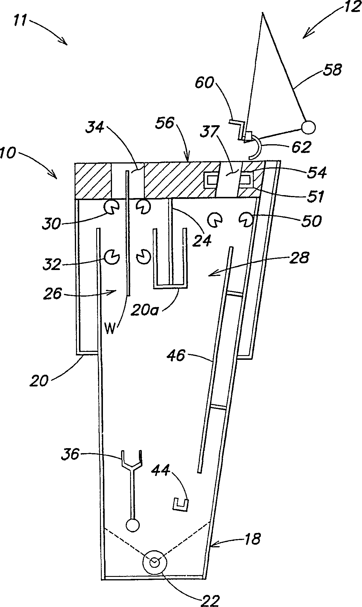
图1所显示的是依据本发明所提出的干燥装置11的结构的侧视图,其中所显示的处理部分和输出部分是依据本发明的第一方案提出。依据本发明所提出的一种干燥装置11包含处理部份10和输出部分12。Fig. 1 shows a side view of the structure of a
处理部-第一方案Processing Department - First Program
处理部分10包含一没入室18a,其将晶片沉浸在例如去离子水的液体浴中,其中可能包含也可能不包含表面活性剂(surfactant)或是其他的化学清洁剂,例如应用材料(Applied Material)公司的ElectraCleanTM溶液。The
上分离壁24(图2A)将没入室18a分隔成两个部分,一个旋干部分26和干燥部分28。借着将干燥部分28与旋干部分26隔离开来,可以获得并维持一个较干净的出口区域,并且可以降低要移除的微粒重新附着于晶片,诸如此类的污染的危险性,因为微粒很容易在此旋干部分26中被移除,并由此被排出。没入室18a可以具有一围绕着没入室18a的溢流堰20,以使得液体得以流入。液体可能持续供应到,例如较低部位的没入室18a,所以液体持续地溢流到溢流堰20。溢流堰20(如图2A至2I所示)可以被耦合到上分离壁24,以帮助由旋干部分26及干燥部分28中移除微粒。(图中所未显示的)高准位和低准位液体传感器可以被耦合到没入室18a以及溢流堰20、20a。在另一个并未显示出来的方案中,溢流堰20可以包含一室,而处理部10则嵌入在其中。排气管线(例如设施排气管线)可以被耦合到此室(例如靠近其底部),并且泄出管线可以被安排于沿着此室底部的位置,其可以被倾斜以加速排除泄出物。The upper separating wall 24 ( FIG. 2A ) divides the
旋干部分26可以装配有顶头喷嘴30,并且/或者没入喷嘴32,前述每一个都是要在晶片进入旋干部分26时,将液体导流到晶片表面上。此旋干部分26,在一方案中,是用来将传送到依据本发明所提出的干燥装置11前已经喷洒于晶片上的任何液体的薄膜(例如表面活性剂)加以旋干。这样的介面活性剂喷洒步骤,已知能防止晶片在送入依据本发明所提出的干燥装置11前其表面的液体就干化而残留。因此在将晶片载入干燥装置前,若有对晶片喷洒以介面活性剂(经常适合使用的是含有低浓度的介面活性剂喷溢,例如Alfonic介面活性剂),将可以避免晶片进入干燥装置前,晶片表面上的液体干化而留下水痕。这样一个依据本发明所提出的步骤可以在清洗装置中或是在晶片传递(例如晶片握持器或是清洗器可以包含将基材施以介面活性剂,以让其在清洗过程中或是在基材被由清洗装置移出,或是在通过晶片握持器传送基材的时候,都能保持其湿润)过程中进行。The spin-drying
旋干部分26可以还包含负载部34,其可以只是一个位置,晶片即是经由此区域进入旋干部分26;或者负载部分也可以是一由旋干部分26的顶部溢流堰或是盖子(若是有盖子的话)所限定的一个开口。The spin-drying
正位于或是靠近没入室18a底部的是托架36,被用于接收或是支持大体是垂直方向的晶片(可能有稍微的与铅直方向有出入),托架36可更进一步地产生一个转动,此转动是由一个托架36可以接收经由负载部34进入旋干部分26的晶片的一个第一位置,转到第二位置,此第二位置是晶片可以被托架36举起,经由干燥部分28的出口部分37的位置离开。当托架36将晶片由旋干部分26转动到干燥部分28时,晶片是保持没入在液体中。Located at or near the bottom of the
通常使用来转动托架36的机构常常是嵌在处理部10的外部上,并且是经由处理部10的外溢流堰,而被直接或是磁吸在耦合到托架36上。在图1例示性的实施例中,当链接系统被启动是往下时,链接系统38可把托架36由第一位置(在旋干部分26中)旋转到第二位置(在干燥部分28中)。当链接系统被启动往上时,链接系统38可把托架36由干燥部分28撤回旋干部分26。所显示的促动器40被耦合到链接系统38上,其中的促动器40可以是任何传统的促动器,例如汽缸等。The mechanism typically used to rotate the
得以驱使托架转动的另一种结构可以包含将托架36嵌于一棍状物上,此棍状物是沿着没入室18a的底部而水平延伸,所以托架36可以沿着该棍状物转动,在这样一个结构中,托架36可以是例如与没入室18a同宽,使得一磁性物质得以同时嵌在前述二者之上,并且可以是经由没入室18a的侧壁而耦合到外部的磁性物质。此外部磁性物质可以被某种促动器(例如气动式的促动器40)向前驱动或是向后驱动。为了使托架36和外部磁性物质转动,滚筒可以被嵌置于其上,以接触并且沿着没入室18a的侧壁滚动。Another structure that can drive the carriage to rotate may include embedding the
一对传感器(未图示)可以被耦合到促动器40、链接系统38以及/或者托架36上,以检测得知第一及第二托架位置。进一步而言,一个传感器,例如光学传感器(未图示)可以检测晶片是否存在于托架36上,一旦检测到晶片存在,则一信号被送到促动器40,以使得促动器40将托架36由第一位置转动到第二位置。A pair of sensors (not shown) may be coupled to
干燥部分28可以包含推进器44,其是被设计成能以最小接触面积来接触晶片的一较低的边缘。这样的一个推进器即是传统所指称的刀缘推进器(knife-edge pushers),此刀缘推进器44可以被耦合到一垂直导引(未图示)上,其是沿着干燥部分28的后壁而放置的,并且可以被进一步(例如磁性地)耦合到促动器(例如一个由马达所驱动的,如图1的铅质螺旋物48)上,其是被用来沿着导引而将推进器44举高或是降低,以至于推进器44得以将晶片由干燥部分28处举起来,并可以在此后让该推进器回到托架36下面的原始位置。Drying
此干燥部分28的后壁通常是倾斜的,(例如,倾斜九度)使得该推进器可以在晶片被由干燥部分28举起时,将该晶片维持在其倾斜的位置,也可以确保晶片位于一较可重复实现的位置,亦即,较一非倾斜的垂直方向更能达成的位置。The rear wall of the drying
一对倾斜导引46也可以被耦合到干燥部分28的后壁,并且其所放置的位置是使其在晶片由托架36经由干燥部分28而被举起时,可以接触晶片的反面边缘。每一个导引46可以包含一个插槽,其可以是U型的或是V型的插槽,而晶片的边缘可以被抓住于其中。或者,每一个导引46可以包含晶片边缘所倚靠的一个斜表面,或是导引46可以形成一个由晶片开始向外远离的角度,以尽可能降低接触面积。A pair of
干燥部分28的出口部分37通常是被限定成干燥部分28的一个顶部墙或是盖子,使得干燥时所产生的蒸气得以由此排出(例如经由泵),而不是由逸散到周围的空气中。在液体准位的上及出口部分37之下,设置有一对的喷洒机构50,其是被用来在晶片被举起而离开液体表面的时候,提供跨过晶片正表面和反面表面的全面连续性的蒸气喷洒。喷洒机构50所摆放的位置是要喷洒蒸气到晶片被由液体中举起时,所形成的凹面上。虽然喷洒机构可能包含一个单一线性喷嘴或是多个喷嘴,其通常包含有一个具有一连串洞孔(例如具有直径0.005至0.007英寸直径的114个洞孔,并且沿着与晶片相邻8.5英寸的距离均匀地分布)形成于其中的管子,前述的喷洒机构(管子)50通常是由石英或是不锈钢所建构而成。The
每一个喷洒机构(管子)50可以是人工手动调整方向,以导流出一个具有预期角度(此角度可以如下所述,相对于经过喷洒管子50中心所画出的水平线,以及垂直于图8A中的液体表面的垂直线)的蒸气流(例如IPA蒸气)。当进一步参照到图6时,此IPA蒸气流的导向,可以有也可以没有气流变流装置的帮助。此气流的特定角度可能视该晶片将要干燥的物质的不同而有所改变,图8B所列出的对照表,是举例所常使用的物质,以及其相对应常使用的气流角度。Each spraying mechanism (pipe) 50 can manually adjust the direction to guide the flow out with a desired angle (this angle can be described below, relative to the horizontal line drawn through the center of the spraying
此被供应到弯液面的IPA蒸气流产生了一个Marangoni力,其引起了与晶片举起方向相反的向下液体流,因此在凹面上的该晶片表面会被干燥。This flow of IPA vapor supplied to the meniscus creates a Marangoni force which causes a downward flow of liquid against the direction of wafer lift, so that the wafer surface on the concave side is dried.
为了要容纳以及排出在干燥部分28内的IPA蒸气,所以提供了废气歧管51和全(blanket)氮气歧管54,这些歧管的制作可以伸入位于喷洒机构50上面的干燥部分28的顶盖56。气流组件(未图示)被耦合到喷洒机构50,废气歧管51和全氮气歧管54控制了IPA蒸气流率、废气流率和氮气遮掩流率。此外废气管线(未图示)可以是被制作在输出部12的下方,经由输出部12可以维持一垂直的流线型的气流,并且可以将由干燥部分28散出的IPA蒸气稀释掉。喷洒机构50通常是被放置在靠近凹面的地方,并且全氮气歧管54通常是被制作在靠近卸载端口37的地方。In order to contain and exhaust the IPA vapors in the
晶片处理-第一方案Wafer Processing -
图2A至图2I是侧面立视图的结构概要图,其显示当晶片被本发明所提出的装置所传送时,该晶片所处的不同阶段。参照图2A,当一机械臂(例如走动横杆机械臂,未于此图示,于公元2000年4月26日送件申请的美国申请专利案第09/558,815号中所揭示,,其一并引用于此)经由负载端口34而将晶片W载入旋干部分26,喷嘴30与喷嘴32,都喷洒去离子水于晶片W的两个面上,此机械臂释放晶片于托架36上,然后由旋干部分26退回其位于负载端口34上方的原始位置。一个光学传感器(未图示)检测到晶片存在于托架36(图2B)上,并且送信号到促动器40,以启动链接系统38,使其由旋干部分26转动到干燥部分28。2A to 2I are side elevation schematic diagrams showing the different stages of the wafer when it is conveyed by the apparatus of the present invention. Referring to FIG. 2A, when a mechanical arm (such as a walking crossbar mechanical arm, not shown here, disclosed in U.S. Patent Application No. 09/558,815 filed on April 26, 2000, one and reference here) the wafer W is loaded into the spin-drying
托架36被制作的位置,是在没入室18a的底部上,或是与前述底部靠近的地方,而其制作的功能是可以传送晶片,由旋干部份26传送到干燥部分28。在此传送过程中,晶片都保持没入在液体面之下,因此托架36为了要接收晶片,由一垂直位置开始转动,为了晶片升高通过干燥部分28(图2C)而转动一个倾斜位置(例如,倾斜9度)。The position that
然后晶片W被举起,经由推进器44以一个举起速度向卸载部37靠近,其举起是以一进行速度(例如每秒十毫米),起始于当晶片顶端没入箱内液体时(此时即是干燥蒸气开始喷洒的时),直到晶片的下缘(例如下面部分的三十至四十毫米的部分的晶片)没入箱内液体。当晶片下缘没入箱内液体中并且通过干燥蒸气时,此晶片会被以一种较慢(例如小于每秒五毫米)的速度举起,因为晶片较低的部分较不好将其干燥(起因于晶片的曲率),在整个晶片干燥后,此晶片可以被以一种较高(例如高于每秒十毫米)的速度举起,以进入到传送位置。当晶片被举起,晶片边缘会因为重力而倚靠在两个平行倾斜引导46上,该导引是沉没在液体中。Then the wafer W is lifted and approaches the unloading
当晶片W被举出液体表面时,该对喷洒机构50(图2D)喷洒IPA蒸气以及氮的混合气体,于晶片W的两面所形成的凹面上。此IPA蒸气流可以借助或是不借助如图6所进一步参照说明的气流变流装置,而得以导引气流方向。此气流的该特定角度,可以视晶片上所要干燥的物质的不同而有所改变。When the wafer W is lifted from the liquid surface, the pair of spraying mechanisms 50 ( FIG. 2D ) spray the mixed gas of IPA vapor and nitrogen on the concave surfaces formed on both sides of the wafer W. The IPA vapor flow can be guided in the direction of the air flow with or without the aid of an air deflector as further described with reference to FIG. 6 . The specific angle of the airflow can vary depending on what is being dried on the wafer.
图8A是一个有助于说明蒸气气流的概略图。参照图8A,如图所示,蒸气/承载气体气流72的流动角度θ是相对于水/空气介面(并且/或者经过喷洒管子50的水平中心线)而量测出来的。(在一较佳实施例中,喷洒管子50是被建构在晶片W侧面水平距离0.5英寸的地方,此时的流动角度被选择在大约25度,并且喷嘴高度是被选择为HN,使得气流72敲击晶片W,大约在晶片/气流介面以上3.7毫米,亦即高度HV的地方。也可使用其他水平间隔、流动角度、喷嘴高度HN以及蒸气敲击高度HV)。图8B表列出例示性物质材料的较佳流动角度(是相对于水/空气介面作测量)。表面物质是指晶片表面上所欲干燥的物质。干进(dry-in)或湿进(wet-in)是指在干燥装置11内处理前的晶片是湿的或是干的,干出(dry-out)表示当晶片由干燥装置11移出时是干的。黑钻石(Black)是一个应用材料公司所可以使用的低k(介电常数)值的介电物质(例如掺杂有碳的氧化物)。IPA蒸气流产生一个″Marangoni″作用力,此会导致与晶片举起方向相反的向下液体流,藉此,在凹面上方的晶片表面会被干燥化。Figure 8A is a schematic diagram to help illustrate vapor flow. 8A, as shown, the flow angle θ of the vapor/
在干燥步骤中,IPA蒸气是经废气歧管51,由处理部分10排出,并且氮气流被导向横跨过输出部分37(经由全氮气歧管54),以制止IPA蒸气逸散出处理部分10。此气体传递组件(未图示)控制IPA蒸气流、废气流率以及全氮气气流流率。During the drying step, IPA vapor is exhausted from the
输出部分-第一方案Output part - first scheme
在如图1至图2I所显示的较佳实施例中,输出部分12包含平台58,是被用于在两个位置之间转动,该二位置是:用于由干燥部分28接收晶片的处理位置(图2E),以及用于输出晶片到传输机械臂的FAB介面位置(图2G)。处理位置是与晶片被由干燥部分28举起的倾斜位置相符,并且处理部份大致而言是为水平的。被耦合到输出部12的马达或是其他驱动机构,可以驱动平台58的转动。In the preferred embodiment, as shown in FIGS. location (FIG. 2E), and the FAB interface location (FIG. 2G) for outputting wafers to the transfer robot. The processing position corresponds to the inclined position where the wafer is lifted by the drying
输出部分12可以包含用来与晶片W被动地移动的捕获器60,其可以被架在线性球切片(linear ball slide)(未图示)上,该线性球切片的每一边的端点上都具有阻挡器。当平台58在处理位置(例如以一个与倾斜的导引46倾斜角相同的角度--九度,向处理部10倾斜)中时,此捕获器60因为重力的因素会掉到线性球切片的底部,可以利用光学传感器(未图示)来检测出此低位。捕获器60可以于两个相隔一距离的点上接触晶片,并且也能够紧密跟随晶片所处环境,而只在一容许误差值内变化,因此捕获器60可以对于精确的晶片定位有所帮助。The
输出部分12也可以包含抓指62(finger 62),用于在晶片固定位置和晶片通行位置之间移动,当其在晶片固定位置,在晶片被举起而位于抓指62之上时,抓指62可以锁住并且固定晶片,因此可以容许推进器44撤回,留下晶片被抓指62和捕获器60固定在输出部分12中的位置上。抓指62可以是,例如汽缸(未图示)所促动,并且配备有一对的开关(未图示)以检测抓指62的晶片固定以及晶片通过位置。也可以利用光学检测器(未图示)来检测何时晶片已经到达抓指62以上足够高的位置,使得抓指62可以安全地假设晶片固定位置。The
晶片输出-第一方案Wafer Output -
在举起晶片W通过干燥部分28前,平台58大致而言是垂直倾斜(例如以一个九度的角度倾斜)(如图2C所示),捕获器60是在其低位置,并且抓指62是在晶片通过位置上。当晶片W离开干燥部分28(如图2D所示),其推动捕获器60(例如接触的两个点),并且导致捕获器60抗拒重力而向上移动。此晶片W因此固定在三点(经由推进器44以及捕获器60)之间,当推进器44到达其高位时,抓指62被启动而来到晶片固定位置,以将晶片固定在平台58上,然后推进器44撤回。(抓指62显示在图2E中的晶片固定位置中)因为捕获器60随着升起的晶片W一起被动地移动,所以在传送进入输出部分12的时候,晶片摩擦和所产生的微粒都得以大量减少。Before lifting the wafer W through the drying
当晶片W被固定在平台58上时,平台58转到其水平位置(如图2F所示),汽缸64(图1),其可包含一可调整式制动器和震动吸收器(未图示),并且可以被用来将平台58降低到一个已定的输出位置,例如,在一个晶片握持器(图2H)可以抽出晶片W处做一升起动作的地方。然后抓指62如图2H所示那样撤回,并且晶片握持器将晶片W拿起以将其转换到另一个位置(例如,转换到卡匣)。然后平台58回到其大体是垂直倾斜的处理位置(图2I),以准备好接收下一个处理好的晶片W′,而使其当被由干燥部分28举起时,作为下一个处理中的晶片W′。When the wafer W is fixed on the
在本发明的较佳实施例或是其他更多的实施例中,可以使用精密的气体传递和废气排放组件(未图示),藉此以传递异丙醇(isopropyl alchol,IPA)蒸气、氮气以及废气到干燥装置11(例如,靠近喷洒机构)。例如干燥而干净的空气伴随以一个或更多个控流管(venturis)(未图示)可以提供其排出(例如气体管线(未图示)可以供应清洁干燥的空气到嵌于卸载端口37附近的控流管的压力部分以供排放)。In the preferred embodiment of the present invention, or other further embodiments, sophisticated gas delivery and exhaust components (not shown) may be used to deliver isopropyl alcohol (IPA) vapor, nitrogen And the exhaust air to the drying device 11 (for example, close to the spraying mechanism). For example, dry and clean air with one or more venturis (not shown) can provide its exhaust (for example, a gas line (not shown) can supply clean dry air to be inserted near the unloading
为了要将IPA/氮气流提供到喷洒机构50,一个质量流控制器(未图示)可以提供一个预设气流量的氮气流,供应到IPA喷口(未图示)。至少在一实施例中,一个1.4公升的喷口被用来传递IPA/氮气混合气体,其具有的成分大约5%的IPA,当然也可以使用其他尺寸的喷口以及/或者其他浓度的IPA。To provide the IPA/nitrogen flow to the
在依据本发明所提出的另一个特定的较佳实施例中,此喷口可以配备有三个准位传感器:低、高以及高-高,首二个准位传感器,被使用的场合可以是,例如,在IPA喷口的自动重新填充期间。而后者的高-高传感器可以被使用的场合是,例如,作为硬件互锁,以避免重新充填时过度填充喷口。一个被加压的供应容器(未图示),例如一公升或是适合容量的容器,可以被使用来对喷口重新填充IPA液体。此供应容器可以包含一个低准位传感器,并且在其低准位传感器被触发时,可以自动地或是人工手动地进行重新填充。In another specific preferred embodiment according to the present invention, the spout can be equipped with three level sensors: low, high and high-high, the first two level sensors can be used, for example , during the automatic refill of the IPA spout. Whereas the latter high-high sensor could be used, for example, as a hardware interlock to avoid overfilling the spout when refilling. A pressurized supply container (not shown), such as a liter or suitable capacity container, can be used to refill the spout with IPA liquid. The supply container can contain a low level sensor and can be refilled automatically or manually when the low level sensor is triggered.
全氮气气流流率(例如为了防止IPA蒸气气流由处理部10逸散而出)可以利用针状阀门或是其他合适的机构加以控制,为了安全的目的,清洁的干燥空气以及全氮气供应管线任一个都可以被加上气流开关(例如当废气或是全氮气气流丧失时,硬件互锁气流开关可以被用来关掉IPA蒸气供应),压力调节器可以被用来控制每一个供应管线中的压力。The full nitrogen gas flow rate (for example to prevent the IPA vapor stream from escaping from the treatment section 10) can be controlled using a needle valve or other suitable mechanism. For safety purposes, clean dry air and full nitrogen supply lines are optional. A gas flow switch can be added to either (for example a hardware interlock gas flow switch can be used to shut off the IPA vapor supply when exhaust or full nitrogen gas flow is lost), and pressure regulators can be used to control the flow rate in each supply line. pressure.
输出部-第二方案Output Department - Second Scheme
图3A至图3B,分别是依据本发明所提出的第二较佳实施例所提出的输出部分12,其概略的侧视图和俯视的概略图。此处依据本发明所提出的图3A至图3B中的装置11a,其包含围绕输出部分12的围体111,输出部分12的可传动平台158可以包含两个或更多个晶片接收器113a及113b,参照图1至图2I,每一个都包含捕获器60和抓指62。在此较佳实施例中,可传动平台158是被用于水平地移动(例如,经由一个铅质螺旋物、汽缸、马达或类似件),所以被由干燥部分28所举起的晶片可以被第一或是第二晶片接收器113a、113b所接收。利用此种方式,得以让晶片产出最大化。当第一晶片可以被第一晶片接收器113a握住,以供晶片握持器(未图示)所提起,而此时第二晶片正被输出到第二晶片接收器113b,反之的亦然。3A to 3B are respectively a schematic side view and a schematic top view of the
此围体111具有可以被建构在邻近于传送机械臂(未图示)的第一侧壁115a,此第一侧壁115a具有开口117,经此开口,传送机械臂可以抽出晶片。围体111也可以具有位置在与第一例壁115a相反的内部分隔壁115b,其用以将围体111分隔成两个气室111a与111b。第一气室111a可以包围可传动平台158,并且也包围了足够空间以容许可传动平台向前或是向后传,并且也可以接收晶片在第一或第二晶片接收器113a与113b上。第二气室111b可以包围用以传递可传动平台158以及任何其他移动部件(大体上由图3B中的参考数字159所代表)的机构。这样分隔两个气室的内部分隔壁115b,可以具有多个小开口119(图3A),其通常涵盖了整个内部分隔壁115b。当相邻于传动机械臂的区域的压力,较相邻于依据本发明所提出的装置11a的区域的压力为高时,空气可能流动式地流动在开口117中,越过第一及第二晶片接收器113a和113b(如箭头F所表示的,平行于晶片的主要表面),并且通过小开口119到达第二气室111b,第二气室111b可以通过废气排放系统而排放废气。The
此外,废气管线(未图示)位于输出部分12之下,经由输出部12维持一可接受的垂直流线型气流,并且也稀释由干燥部分28逸散而出的任何IPA蒸气。输出部分112的围体111作用如一外加的污染机构,以防止IPA蒸气进入环绕干燥装置11a周围的空气中。Additionally, an exhaust line (not shown) is located below
为了要容许晶片可以被输出到第一晶片接收器113a,而不会阻挡主容箱118的旋干部分26,主容箱118的前壁121(也就是旋干部分26的前壁),可以如图3所示那样,使其具有一定角度(例如九度)。通过将旋干部分26的前壁弯曲一角度,负载端口34将可以被制作在一个离输出部分37足够远的地方,以避免被围体111所阻挡,但是处理部分10的液体体积的增加,并没有和使用直的前壁时所会增加的体积一样多。在使用前述具有角度前壁的实施例中,托架36可以被举起到一个靠近负载端口34的位置,使得晶片握持器可以放置晶片于被举起的托架36。这样一个举起的托架36,容许使用没有能力转动以让负载端口34和处理部分10角度符合的晶片握持器。这一个可提高的托架36可以被耦合到一个导引,此导引的位置是沿着具有某角度的前壁的内部表面,并且经由前壁可以磁性地耦合到外部促动器,并且因此可以与可提高的推进器44具有相类似的运作方式。In order to allow wafers to be output to the
晶片输出-第二方案Wafer Output -
图4A至图4I,是显示晶片在如图3A到图3B所显示的另一个不同的装置11a,于不同的处理阶段时的概略的侧视图,如图4A所示,晶片W1被放置在输出平台158的晶片接收器113a上,并且输出平台158是在其最右边的位置,而第二晶片接收器113b被放置的位置,是使其可以接收由干燥部分28所输出的晶片。晶片W2是被放置在没入的托架36上,并且推进器44所在的位置是在托架36下方。在图4B中,推进器44被举高(例如经由托架36中的槽或是开口),以由托架36上举起晶片W2,并且托架36已经被转回到垂直位置。4A to 4I are schematic side views showing wafers at different processing stages in another
在图4C中,推进器44已经到达升高的位置,此位置是晶片W2通过卸载端口37的位置,并且晶片W2的顶缘接触到捕获器60。当晶片W2移动进入卸载端口37,IPA蒸气喷洒、全氮气以及废气开始启动,图4C也显示托架36已经举起,并且被放置在负载端口34中,以准备好接收下一个要进入的晶片。In FIG. 4C ,
如图4D所示,第一晶片W1已经被由围体111的第一晶片接收器113a所抽出,并且捕获器60已经回其较低的位置,第二晶片W2已经提升到第二晶片接收器113b上的一个抓指62的上方,抓指62已经移动进入到第二晶片W2的下方,并且推动器44已经降低其位置,并不在支持第二晶片W2,其于此时是被握持在抓指62和捕获器60之间。第三晶片W3被负载在托架36之上,并且托架36已经降低到处理部10的底部,值得注意的是因为第三晶片W3经由可能是在被没入喷嘴32以及/或是未没入喷嘴30(未图示)所喷洒的负载端口34而降低其位置。As shown in Figure 4D, the first wafer W1 has been drawn out by the
如图4E所示,平台158被移动到其最左侧的位置,使第一晶片接收器113a所处的位置能够接收由干燥部份28所输出的晶片,此推进器44已经降低到一个位置低于托架36所提高,并且托架36将会旋转第三晶片W3,使其由旋干部分26到干燥部分28。As shown in Figure 4E, the
如图4F所示,托架36转动到干燥部分36中的第三晶片W3的位置,并且第三晶片W3的上侧部分停驻在晶片导引46上。As shown in FIG. 4F , the
如图4G所示,推进器44已经升高,举起托架36的第三晶片W3而升高,并且托架36转动而回到一个垂直位置。As shown in FIG. 4G, the
如图4H所示,经由IPA蒸气喷洒,推进器44开始举起第三晶片W3而升高,并且经由全氮气,到达第三晶片W3的顶端接触到第一晶片接收器113a的捕获器60。该托架36已经举高,以将其本身放到负载端口34中,以准备好接收下一个要进入的晶片。As shown in FIG. 4H , through the IPA vapor spraying, the
如图4I所示,第二晶片W2已经由输出围体111的第二晶片接收器113b所抽出,并且捕获器60已经回到其较低的位置,此第三晶片W3已经被举起在第一晶片接收器113a上,而到达抓指62上方,抓指62已经移动进入第三晶片W3之下的位置,并且推进器44已经降低其位置,已不再支持第三晶片W3,其此时被握持在介于抓指62和捕获器60之间的位置。第四晶片W4负载到托架36之上,并且托架36已经降低到旋干部分10的底部上,值得注意的是因为第三晶片W4经由可能是在被没入喷嘴32以及/或是未没入喷嘴(未图示)所喷洒的负载端口34而降低其位置。As shown in Figure 4I, the second wafer W2 has been extracted by the
处理部份-第二方案Processing part - second option
图5是为依据本发明所提出的一个干燥装置211的侧视概略图,其中只显示处理部份10。此处理部份10是依据本发明所提出的第二个方案所建构,特别的是不使用要浸入晶片(例如显示于图1至图2I的没入室18a)的主室。在本发明所提出的第二方案中,主室对以液体对于未没入的晶片喷洒,以旋干并且/或是维持在旋干气室226中的晶片的潮湿度,并且以液体对于未没入的晶片进行喷洒,以产生在干燥器室228中的弯液面(用于Marangoni干燥方法)。只有少数硬件差异存在于为了没入器室处理方式所建构的处理部分,以及为了非没入器室处理方式所建构的处理部分之间?FIG. 5 is a schematic side view of a
如参照图5所可以看见的,图1至图2I的溢流溢流堰20和20a可以被省略,通常所使用的一对顶头喷嘴30所制作的位置,是使得当晶片进入而经过负载端口34时,其可以对晶片的前表面和后表面都喷洒液体。在图5所显示的较佳实施例中,隔离墙24制止了所喷洒的液体由旋干部分226溅入到干燥部分228所提供的液体喷嘴上方的区域(并因此制止了已经干燥的晶片不小心被重新弄湿)。在干燥部分228中,一个额外的液体供应喷洒机构50a被提供在IPA供应喷洒机构50之下。As can be seen with reference to FIG. 5, the
在操作时,正在进入的晶片被喷洒的液体,例如去离子水,其可以有或没有包含介面活性剂,或是其他清洁用的化学药剂,例如应用材料公司的ElectraCleanTM溶液,以用于旋干以及/或是维持晶片表面的潮湿度。当晶片离开干燥部分228时,晶片被喷洒以例如去离子水的液体,其中可以掺杂或是不掺杂介面活性剂或是其他清洁剂,此出口液体喷洒形成了一个横跨晶片的均匀弯液面。此IPA喷洒机构50喷洒IPA蒸气到凹面上,因此创造了可以将晶片干燥化的Marangoni流。值得注意的是晶片传输是在处理部10,并且晶片输出到输出部分12可以如图1至图4I所描述的那样。In operation, the incoming wafer is sprayed with a liquid, such as deionized water, which may or may not contain surfactants, or other cleaning chemicals, such as Applied Materials' ElectraClean ™ solution, for spin dry and/or maintain the wetness of the wafer surface. As the wafer exits the
气流变流装置air deflector
IPA蒸气传送到水/空气/水介面(亦即凹面)的效率,可以因为对于每个IPA传递蒸气喷嘴/管50建立蒸气气流变流装置而获得改善,一个这样建构的装置的概略图显示在图6中。虽然在实务上的喷管50以及气流变流装置68,可以被提供在晶片W的每一个侧边,为了绘制上的简化,喷管50(可以包含上述的喷嘴50)以及气流变流装置68只显示在晶片W的一个侧边上。虽然晶片W可以用一个倾斜角(虽然可以使用其他的角度,但是在此例中是利用为垂直线算起约九度的角度)离开水76的表面,晶片W也可以如图所示的,离开垂水76时,是垂直于其表面的。The efficiency of IPA vapor delivery to the water/air/water interface (i.e. concave surface) can be improved by creating a vapor flow deflector for each IPA delivery vapor nozzle/
在本发明所提出的一较佳实施例中,气流变流装置68可以利用两个部分套管的形式,其是用于配合喷嘴50,气流变流装置68限定出一个楔型空间70,一股气流的IPA蒸气(例如混杂以氮气的承载气体)被喷洒,并且被设计将气流72以一特定的角度导流入楔形空间70中,此角度是相对于,例如经过喷嘴50中心并且平行于水表面,的一条水平线L。气流变流装置68的第二区域(例如低翼74)可以浸(dip)在水76的下面,以限制水暴露在IPA蒸气下的部分的体积。IPA蒸气的气流72通常是使用向下的角度,如图6所示那样,打在气流变流装置68的第一区域69的内部表面78。然后IPA蒸气的气流72可以被内部表面78反射(未图示)到形成于水/空气/水介面的凹面80上。在本发明所提出的一个或更多的较佳实施例当中,IPA气流72与内部表面78之间的角度并不会超过四十五度,虽然IPA气流72角度的选择,通常是使得IPA气流以一个预期的角度范围内(如以下所述并参照图8A到图8B)打在凹面80上,并且/或是以一个预期的气流速度使得IPA蒸气传递到凹面80上得以最佳化。In a preferred embodiment proposed by the present invention, the
在一个用以说明本发明而举例的实施例中,气流变流装置68具有一个细缝开口82,其宽度可以是0.05英寸,并且细缝可以是被隔开的,例如远离晶片W达0.1英寸的地方,使其有效率地传递IPA蒸气到凹面80。同理,对于其他宽度的细缝、在水76表面上方不同距离以及/或者与晶片W具不同的距离,这些上述条件也都可以适用。气流变流装置68可以位于对于水76表面具有四十五度的一个角度上,然而也可以利用其他的角度。细缝开口82的角度通常会被定在刚好位于凹面80下方。In one exemplary embodiment to illustrate the present invention, the
此气流变流装置68是用以限制曝露在IPA蒸气下的水的体积,因此可以降低IPA的浪费和使用量,同时也改进了干燥器效率以及其性能,并且降低了安全性的风险。在依据本发明所提出的一较佳实施例中,虽然其他数据仍能进行,但是一般而言,对于300毫米的晶片而言,曝露在IPA蒸气下的水的体积的范围大约是零至十二毫升(milliliter),对于200毫米的晶片而言,曝露在IPA蒸气下的水的体积的范围大约是零至八毫升。The
若没有使用气流变流装置68,IPA蒸气的气流72可以在一角度范围上,约为22度到30度,打在水76表面上,此已经被发现适合于形成在晶片上的数个不同种类的薄膜的干燥化工序,其他入射角也可以使用在本发明中。此气流变流装置68可以用单一个整体物件,或者是两个以上的物件合并而成,气流变流装置68可以由不锈钢或是其他适合的物质来作成。If the
低浓度的IPA混合气体Low concentration of IPA mixed gas
要进一步改善此清洁/干燥化组件的安全性以及效率,可以降低IPA/负载气体的混合气体中的IPA蒸气浓度(例如降低到0.2%),同时也可以增加混合气体的气体流率(例如至少每分钟二至三公升,常常使用的是每分钟五公升)。此增加的气流流率补偿了低浓度的IPA气体,并且也因此达到高效率以及高干燥率下的低缺陷的干燥工序(使得200毫米的晶片,在假设都是使用相同的晶片升高速度的条件下,例如每秒十毫米,其干燥时间是20秒)。图7是一个画出了具有粒径0.12微米(图3中,一般称的)的粒子的数目的图形,其为发现于被气体(氮)干燥的晶片上,其中的气体具有不同的IPA浓度和不同的气流流率。结果可能也因为喷嘴直径、喷嘴相隔于晶片表面的距离、气流变流装置的使用及角度等因素而有不同。对于每分钟五公升的承载气体流率所做的实验性数据,显示当IPA蒸气的浓度由1%降低到0.2%时,硅上面的缺陷和包含晶片的低k介电物质上面的缺陷,并没有增加。To further improve the safety and efficiency of this cleaning/drying assembly, the IPA vapor concentration in the mixed gas of IPA/carrying gas can be reduced (for example, down to 0.2%), and the gas flow rate of the mixed gas can also be increased (for example, at least 2 to 3 liters per minute, 5 liters per minute is often used). This increased gas flow rate compensates for the low concentration of IPA gas, and thus achieves a high efficiency and low-defect drying process at a high drying rate (making 200mm wafers, assuming that the same wafer raising speed is used) Under conditions, such as ten millimeters per second, the drying time is 20 seconds). Figure 7 is a graph plotting the number of particles having a particle size of 0.12 microns (commonly referred to in Figure 3) as found on wafers dried by gas (nitrogen) with varying concentrations of IPA and different air flow rates. Results may also vary due to factors such as nozzle diameter, distance of the nozzle from the wafer surface, use and angle of the aerofluidic device, etc. Experimental data for a carrier gas flow rate of five liters per minute showed that when the concentration of IPA vapor was reduced from 1% to 0.2%, defects on the silicon and on the low-k dielectric containing the wafer, and No increase.
如前面所叙述的,当晶片W的较低部分被干燥时,晶片举起速度可以被降低。相似地,当晶片W的较低部分已经干燥化时,在IPA/承载气体混合气体中的IPA浓度可以增加,并且/或者IPA/承载气体混合气体的气流流率可以增加。如众所周知的,以上的氮气可以被其他惰性气体所取代仍能正常进行制作工序,而同时广为了解的是,IPA可以被其他传统用于Marangoni干燥工序等的有机气体所取代,并仍能正常进行制作工序。As previously stated, when the lower portion of the wafer W is dried, the wafer lift speed can be reduced. Similarly, when the lower portion of the wafer W has been dried, the IPA concentration in the IPA/carrier gas mixture may be increased and/or the flow rate of the IPA/carrier gas mixture may be increased. As is well known, the above nitrogen can be replaced by other inert gases and the production process can still be carried out normally. At the same time, it is widely known that IPA can be replaced by other organic gases traditionally used in the Marangoni drying process, etc., and still work normally. Carry out the production process.
当此发明连同其所描述的较佳实施例被揭示之后,其他的实施例如众所周知的,也都落在本发明的精神和范围中。特别的是,本发明所提出的用来举起的机制,以及本发明所提出的IPA气流变流装置,显然地可以被使用在任何干燥化系统中,并且不限定只能使用在所揭示的系统中。相似地,当基材进入旋干工序箱中时,可以使用喷嘴(水下的以及/或是水/液体面之上的)来进行旋干工序,然而也可以用在本发明实施例所揭示以外的系统中。具有一倾斜角度的室壁,配合以用一已知方向输出晶片的组件,被认为是具有发明性的,作为一个被动的输出捕获器。更进一步的发明特征,其包含用于传送晶片(特别是一个没入液体中的晶片),由第一角度在传送过程中转变到到第二角度的组件与方法,也包含一个组件,其用于传送晶片,由一个角度到下一个角度,以移动该晶片由对齐一输入部分,到此晶片对其输出部分。因此,所能被了解的是,在此所描述的所有实施例只是解说举例,并且本发明所提出的装置可以使用以下的一个或多个特征。While the invention has been disclosed with its described preferred embodiments, other embodiments, as known, fall within the spirit and scope of the invention. In particular, the lifting mechanism proposed by the present invention, as well as the IPA aerofluidic device proposed by the present invention, can obviously be used in any desiccation system, and are not limited to be used only in the disclosed system. Similarly, nozzles (underwater and/or above the water/liquid surface) can be used to perform the spin-drying process when the substrate enters the spin-drying chamber, but can also be used in the in other systems. The assembly of chamber walls having a sloped angle, in cooperation with outputting wafers in a known direction, is believed to be inventive as a passive output catcher. Further inventive features include an assembly and method for transferring a wafer, particularly a wafer submerged in a liquid, from a first angle to a second angle during transfer, and also includes an assembly for Transfers the wafer, from one angle to the next, to move the wafer from aligned to an input section, to the wafer to its output section. Therefore, it is to be understood that all embodiments described herein are illustrative examples only, and that the proposed device of the present invention may utilize one or more of the following features.
有些能被单独使用的发明特征如下所述:Some of the inventive features that can be used on their own are as follows:
●结合旋干部分和干燥部分,而没有旋干的晶片表面曝露在空气中的一个组件;An assembly that combines a spin-drying section and a drying section, without the spin-drying wafer surface being exposed to air;
●配备有用于改善移除介面活性剂和制作工序箱微粒(顶头喷嘴提供了最有效的旋干)的没入以及/或是顶头喷嘴的一个旋干部分;Equipped with a submersion and/or a spin-drying section of the top nozzle for improved removal of surfactants and process tank particles (the top nozzle provides the most efficient spin-drying);
●具有两个部分,以分开负载和卸载部分的一个主要制作工序箱;A main fabrication process box with two sections to separate the loading and unloading sections;
●管子、喷嘴以及/或是气流变流装置,用于精确地递送IPA蒸气(例如传送到弯液面的顶端),以将IPA的消耗最小化;- tubes, nozzles, and/or aerodynamic devices for precise delivery of IPA vapor (e.g., to the top of the meniscus) to minimize consumption of IPA;
●IPA喷洒管子,可以被精确地位于一个最佳角度方向上,以供应IPA到弯液面上;(参照申请日为2001年3月5日的、发明名称为喷洒棒的美国专利第60/273,786号,现一并引用于此);The IPA spray pipe can be precisely located on an optimal angle direction to supply IPA to the meniscus; (with reference to the U.S. Patent No. 60 / 273,786, hereby incorporated by reference);
●不碎裂的导引机构,其使用嵌入输出站顶端的一个″捕获器″;Non-fragmentation guiding mechanism using a "catch" embedded in the top of the output station;
●托架,简化水面下晶片由旋干部传递到干燥部的过程;●The bracket simplifies the transfer process of the wafer under the water surface from the spinning part to the drying part;
●可变速度推进器,其具有一个提高速度机构;A variable speed propeller with a speed increasing mechanism;
●倾斜的后壁以及/或是倾斜的前壁;a sloped rear wall and/or a sloped front wall;
●内部溢流溢流堰,用于具有分离的输入和输出部分的制作工序箱;An internal overflow overflow weir for fabrication process boxes with separate input and output sections;
●具有流线型气流的被包围的输出;●Enclosed output with streamlined airflow;
●变流器,用于限制曝露在干燥化(例如IPA)蒸气的液体的表面的面积;Current transformers to limit the surface area of the liquid exposed to desiccated (eg IPA) vapors;
●使用限流管的排放,用于稀释有机溶剂的浓度;Use the discharge of the restrictor tube to dilute the concentration of organic solvents;
●干燥化混合气体的使用,其具有被降低浓度的有机溶剂,并被提高空气流率;● the use of desiccated gas mixtures with reduced concentrations of organic solvents and increased air flow rates;
●多个输出晶片支持器,用于由干燥器而来的至少部分的同时输出,并且以机械臂取拾;以及a plurality of output wafer holders for at least some simultaneous output from the dryer and picked up by a robotic arm; and
●一个组件,具有旋干部分,以及可以在其内部使用Marangoni干燥方法的部分,前述两个部分皆使用喷洒机构而不是使用晶片没入处理。• An assembly with a spin-dried part and a part inside which the Marangoni drying method can be used, both using a spray mechanism instead of a wafer submersion process.
与传统的SRD比较,本发明所提出的装置11可以提供特别优越的表现,并在将斥水性或是亲水性晶片进行干燥工序时,都容许较大的制作工序误差。此新的植基于″Marangoni″原理的干燥技术,以下仅为举例说明,可以只留下3奈米(neon-meter)厚的层,相对的,传统的SRD所会留下的是大约200奈米厚的层。通过将处理组件与输出站结合,本发明所提出的装置可以快速的干燥,以致对于各种不同的薄膜种类的晶片的干燥工序,都可以具有高产出。此旋干部分喷嘴,也有能力去除可能在刷洗以及传送到干燥组件时,被施于斥水性晶片表面的介面活性剂。Compared with the traditional SRD, the
应该注意的是全氮气只是举例说明,并且任何的惰性气体或是空气或是或是多种气体混合,都可以用来形成横越过输出部分的一个包围,并且接着制止干燥蒸气由此装置逸散出去。也应该注意的是IPA蒸气也只是举例说明所用的,并且可以溶解于液体(被施于干燥部分中)的其他蒸气或气体,其用于产生可将干燥化的Marangoni气流,这些气体都可以使用在本发明中。因此这样的蒸气或是气体在此将会被指认为干燥化气体。在此揭示时所使用的词句″捕获器″、″抓指″以及″托架″,并非用以限定本发明的相应物件到特定的形状或结构,而是广泛地指称任何与在此所描述的捕获器、抓指以及托架,具有相同功能的结构的物件。It should be noted that full nitrogen is by way of example only, and that any inert gas, or air, or a mixture of gases, may be used to form an enclosure across the output section and then prevent dry vapor from escaping from the device. go out. It should also be noted that the IPA vapor is used for illustration only, and that other vapors or gases that can be dissolved in the liquid (applied to the dry part) that are used to generate the dry Marangoni stream can be used In the present invention. Such vapors or gases will therefore be referred to herein as desiccated gases. The words "catch", "finger" and "bracket" used in this disclosure are not intended to limit the corresponding objects of the present invention to a specific shape or structure, but generally refer to any The catcher, finger and bracket of the same function structure.
虽然本发明已参照当前的具体实施例来描述,但是本技术领域中的普通技术人员应当认识到,以上的实施例仅是用来说明本发明,在没有脱离本发明精神的情况下还可作出各种等效的变化或替换,因此,只要在本发明的实质精神范围内对上述实施例的变化、变型都将落在本申请的权利要求书的范围内。Although the present invention has been described with reference to the current specific embodiments, those of ordinary skill in the art should recognize that the above embodiments are only used to illustrate the present invention, and other modifications can be made without departing from the spirit of the present invention. Various equivalent changes or substitutions, therefore, as long as the changes and modifications to the above embodiments are within the spirit of the present invention, they will all fall within the scope of the claims of the present application.
Claims (28)
Applications Claiming Priority (2)
| Application Number | Priority Date | Filing Date | Title |
|---|---|---|---|
| US33533501P | 2001-11-02 | 2001-11-02 | |
| US60/335,335 | 2001-11-02 |
Related Parent Applications (1)
| Application Number | Title | Priority Date | Filing Date |
|---|---|---|---|
| CNB028219694A Division CN100477071C (en) | 2001-11-02 | 2002-11-01 | Drying device and drying method for single wafer |
Publications (2)
| Publication Number | Publication Date |
|---|---|
| CN101499413A CN101499413A (en) | 2009-08-05 |
| CN101499413B true CN101499413B (en) | 2011-05-04 |
Family
ID=23311345
Family Applications (5)
| Application Number | Title | Priority Date | Filing Date |
|---|---|---|---|
| CN2009101281209A Expired - Fee Related CN101499413B (en) | 2001-11-02 | 2002-11-01 | Single wafer dryer and drying methods |
| CN2008101660361A Expired - Fee Related CN101414547B (en) | 2001-11-02 | 2002-11-01 | Method for cleaning microelectronic device |
| CN2008101660376A Expired - Fee Related CN101414548B (en) | 2001-11-02 | 2002-11-01 | Single wafer drying device and drying method |
| CNB028219694A Expired - Lifetime CN100477071C (en) | 2001-11-02 | 2002-11-01 | Drying device and drying method for single wafer |
| CN200710103401XA Expired - Fee Related CN101086955B (en) | 2001-11-02 | 2002-11-01 | Single wafer dryer and drying methods |
Family Applications After (4)
| Application Number | Title | Priority Date | Filing Date |
|---|---|---|---|
| CN2008101660361A Expired - Fee Related CN101414547B (en) | 2001-11-02 | 2002-11-01 | Method for cleaning microelectronic device |
| CN2008101660376A Expired - Fee Related CN101414548B (en) | 2001-11-02 | 2002-11-01 | Single wafer drying device and drying method |
| CNB028219694A Expired - Lifetime CN100477071C (en) | 2001-11-02 | 2002-11-01 | Drying device and drying method for single wafer |
| CN200710103401XA Expired - Fee Related CN101086955B (en) | 2001-11-02 | 2002-11-01 | Single wafer dryer and drying methods |
Country Status (7)
| Country | Link |
|---|---|
| US (6) | US6955516B2 (en) |
| EP (1) | EP1446827A2 (en) |
| JP (1) | JP4296090B2 (en) |
| KR (2) | KR20080095310A (en) |
| CN (5) | CN101499413B (en) |
| TW (1) | TWI285911B (en) |
| WO (1) | WO2003041131A2 (en) |
Families Citing this family (53)
| Publication number | Priority date | Publication date | Assignee | Title |
|---|---|---|---|---|
| US6328814B1 (en) * | 1999-03-26 | 2001-12-11 | Applied Materials, Inc. | Apparatus for cleaning and drying substrates |
| US7513062B2 (en) * | 2001-11-02 | 2009-04-07 | Applied Materials, Inc. | Single wafer dryer and drying methods |
| CN101499413B (en) * | 2001-11-02 | 2011-05-04 | 应用材料股份有限公司 | Single wafer dryer and drying methods |
| US20080000495A1 (en) * | 2001-12-07 | 2008-01-03 | Eric Hansen | Apparatus and method for single substrate processing |
| US20090029560A1 (en) * | 2001-12-07 | 2009-01-29 | Applied Materials, Inc. | Apparatus and method for single substrate processing |
| US20040031167A1 (en) | 2002-06-13 | 2004-02-19 | Stein Nathan D. | Single wafer method and apparatus for drying semiconductor substrates using an inert gas air-knife |
| US20040200409A1 (en) * | 2002-12-16 | 2004-10-14 | Applied Materials, Inc. | Scrubber with integrated vertical marangoni drying |
| US7244315B2 (en) * | 2003-06-27 | 2007-07-17 | Fsi International, Inc. | Microelectronic device drying devices and techniques |
| JP4248989B2 (en) | 2003-10-10 | 2009-04-02 | 大日本スクリーン製造株式会社 | High pressure processing apparatus and high pressure processing method |
| US20060003570A1 (en) * | 2003-12-02 | 2006-01-05 | Arulkumar Shanmugasundram | Method and apparatus for electroless capping with vapor drying |
| KR100634374B1 (en) * | 2004-06-23 | 2006-10-16 | 삼성전자주식회사 | Apparatus and method for drying a substrate |
| US7127830B2 (en) * | 2004-08-02 | 2006-10-31 | Wafertech, Llc | Reticle carrier apparatus and method that tilts reticle for drying |
| JP4758846B2 (en) * | 2005-11-18 | 2011-08-31 | 東京エレクトロン株式会社 | Drying apparatus, drying method, and drying program, and substrate processing apparatus, substrate processing method, and substrate processing program having the same |
| JP4580327B2 (en) * | 2005-11-21 | 2010-11-10 | 東京エレクトロン株式会社 | Method of taking out object to be processed, program storage medium, and mounting mechanism |
| JP4901395B2 (en) * | 2006-09-26 | 2012-03-21 | 富士フイルム株式会社 | Drying method of coating film |
| KR101433868B1 (en) * | 2006-10-02 | 2014-08-29 | 램 리서치 아게 | Apparatus and method for removing liquid from a surface of an object, such as a disc |
| US7980000B2 (en) | 2006-12-29 | 2011-07-19 | Applied Materials, Inc. | Vapor dryer having hydrophilic end effector |
| US20080155852A1 (en) * | 2006-12-29 | 2008-07-03 | Olgado Donald J K | Multiple substrate vapor drying systems and methods |
| US7694688B2 (en) | 2007-01-05 | 2010-04-13 | Applied Materials, Inc. | Wet clean system design |
| US20080163900A1 (en) * | 2007-01-05 | 2008-07-10 | Douglas Richards | Ipa delivery system for drying |
| US7950407B2 (en) | 2007-02-07 | 2011-05-31 | Applied Materials, Inc. | Apparatus for rapid filling of a processing volume |
| US20080293329A1 (en) * | 2007-05-21 | 2008-11-27 | Applied Materials, Inc. | Methods and apparatus for identifying a substrate edge profile and adjusting the processing of the substrate according to the identified edge profile |
| US20090205686A1 (en) * | 2008-02-19 | 2009-08-20 | United Microelectronics Corp. | Wafer cleaning apparatus |
| US8002901B1 (en) | 2009-01-15 | 2011-08-23 | Wd Media, Inc. | Temperature dependent pull speeds for drying of a wet cleaned workpiece |
| JP5140641B2 (en) * | 2009-06-29 | 2013-02-06 | 株式会社荏原製作所 | Substrate processing method and substrate processing apparatus |
| US20110289795A1 (en) | 2010-02-16 | 2011-12-01 | Tomoatsu Ishibashi | Substrate drying apparatus, substrate drying method and control program |
| US20120306139A1 (en) | 2011-06-03 | 2012-12-06 | Arthur Keigler | Parallel single substrate processing system holder |
| WO2013162638A1 (en) * | 2012-04-26 | 2013-10-31 | Applied Materials, Inc. | Vapor dryer module with reduced particle generation |
| US8869422B2 (en) | 2012-04-27 | 2014-10-28 | Applied Materials, Inc. | Methods and apparatus for marangoni substrate drying using a vapor knife manifold |
| CN102914139B (en) * | 2012-10-19 | 2015-12-09 | 上海华虹宏力半导体制造有限公司 | Drying wafer equipment and forming method thereof |
| CN103909072A (en) * | 2013-01-07 | 2014-07-09 | 台湾暹劲股份有限公司 | Electronic element washing device and operation device used by same |
| CN103017483A (en) * | 2013-01-11 | 2013-04-03 | 彩虹(佛山)平板显示有限公司 | Drying method of mask after cleaning |
| JP6351993B2 (en) * | 2013-03-18 | 2018-07-04 | 芝浦メカトロニクス株式会社 | Substrate processing apparatus and substrate processing method |
| US9728428B2 (en) * | 2013-07-01 | 2017-08-08 | Applied Materials, Inc. | Single use rinse in a linear Marangoni drier |
| US9922801B2 (en) | 2013-08-23 | 2018-03-20 | Mapper Lithography Ip B.V. | Drying apparatus for use in a lithography system |
| NL2011710C2 (en) * | 2013-10-31 | 2015-05-04 | F G J Lammertink Beheer B V | Device for cleaning a stylus of a measuring probe. |
| KR20160026302A (en) * | 2014-08-29 | 2016-03-09 | 삼성전자주식회사 | Substrate processing apparatus, apparatus for manufacturing integrated circuit device, substrate processing method and method of manufacturing integrated circuit device |
| US9984867B2 (en) * | 2014-12-19 | 2018-05-29 | Applied Materials, Inc. | Systems and methods for rinsing and drying substrates |
| US9352471B1 (en) | 2015-01-21 | 2016-05-31 | Applied Materials, Inc. | Substrate gripper apparatus and methods |
| CN107845590B (en) * | 2017-11-02 | 2020-03-31 | 德淮半导体有限公司 | Cleaning device |
| CN111602021B (en) * | 2017-11-13 | 2024-08-30 | 振兴电子有限责任公司 | Method and apparatus for drying electronic equipment |
| US11430672B2 (en) | 2019-03-04 | 2022-08-30 | Applied Materials, Inc. | Drying environments for reducing substrate defects |
| CN109887865B (en) * | 2019-03-07 | 2021-08-20 | 上海华力微电子有限公司 | Wafer cleaning and drying device and method and chemical mechanical polishing machine |
| CN111092036B (en) * | 2020-03-23 | 2020-07-14 | 杭州众硅电子科技有限公司 | A wafer cleaning and drying device |
| US11682567B2 (en) | 2020-06-30 | 2023-06-20 | Applied Materials, Inc. | Cleaning system with in-line SPM processing |
| CN111540702B (en) * | 2020-07-10 | 2020-09-29 | 清华大学 | Vertical marangoni wafer processing device |
| CN111785663B (en) * | 2020-07-10 | 2023-02-28 | 华海清科股份有限公司 | Wafer post-processing system |
| CN111900109A (en) * | 2020-07-23 | 2020-11-06 | 华虹半导体(无锡)有限公司 | CMP cleaning and drying device |
| KR102360343B1 (en) * | 2020-10-07 | 2022-02-09 | 주식회사 한양티에스 | Unit type test printed circuit board cleaning and drying device |
| US12198944B2 (en) | 2020-11-11 | 2025-01-14 | Applied Materials, Inc. | Substrate handling in a modular polishing system with single substrate cleaning chambers |
| CN214747111U (en) * | 2021-01-22 | 2021-11-16 | 京东方科技集团股份有限公司 | Air drying device |
| KR20240121815A (en) * | 2021-12-22 | 2024-08-09 | 후지필름 일렉트로닉 머티리얼스 유.에스.에이., 아이엔씨. | Method for reducing defects in polished wafers |
| US20250336692A1 (en) * | 2024-04-25 | 2025-10-30 | Yield Engineering Systems, Inc. | Unified rinse and dry cleaning apparatus and methods |
Family Cites Families (118)
| Publication number | Priority date | Publication date | Assignee | Title |
|---|---|---|---|---|
| US3868272A (en) * | 1973-03-05 | 1975-02-25 | Electrovert Mfg Co Ltd | Cleaning of printed circuit boards by solid and coherent jets of cleaning liquid |
| US4647266A (en) * | 1979-12-21 | 1987-03-03 | Varian Associates, Inc. | Wafer coating system |
| JPS58182235A (en) | 1982-04-19 | 1983-10-25 | Nippon Texas Instr Kk | Wafer washing apparatus |
| US4569695A (en) * | 1983-04-21 | 1986-02-11 | Nec Corporation | Method of cleaning a photo-mask |
| US4534314A (en) * | 1984-05-10 | 1985-08-13 | Varian Associates, Inc. | Load lock pumping mechanism |
| US4548699A (en) * | 1984-05-17 | 1985-10-22 | Varian Associates, Inc. | Transfer plate rotation system |
| US4911761A (en) * | 1984-05-21 | 1990-03-27 | Cfm Technologies Research Associates | Process and apparatus for drying surfaces |
| US4984597B1 (en) * | 1984-05-21 | 1999-10-26 | Cfmt Inc | Apparatus for rinsing and drying surfaces |
| US4778532A (en) * | 1985-06-24 | 1988-10-18 | Cfm Technologies Limited Partnership | Process and apparatus for treating wafers with process fluids |
| US4633893A (en) * | 1984-05-21 | 1987-01-06 | Cfm Technologies Limited Partnership | Apparatus for treating semiconductor wafers |
| US4790155A (en) * | 1986-11-18 | 1988-12-13 | Burlington Industries, Inc. | Replaceable fluid dye applicator for inert-blanketed regions |
| NL8900480A (en) | 1989-02-27 | 1990-09-17 | Philips Nv | METHOD AND APPARATUS FOR DRYING SUBSTRATES AFTER TREATMENT IN A LIQUID |
| US5045120A (en) * | 1989-03-06 | 1991-09-03 | Electrovert Ltd. | Method for cleaning electronic and other devices |
| US5115576A (en) * | 1989-10-27 | 1992-05-26 | Semifab Incorporated | Vapor device and method for drying articles such as semiconductor wafers with substances such as isopropyl alcohol |
| US4977688A (en) * | 1989-10-27 | 1990-12-18 | Semifab Incorporated | Vapor device and method for drying articles such as semiconductor wafers with substances such as isopropyl alcohol |
| JPH0418436A (en) | 1990-05-11 | 1992-01-22 | Mitsubishi Kasei Corp | Production of porous resin |
| US5082518A (en) * | 1990-10-29 | 1992-01-21 | Submicron Systems, Inc. | Sparger plate for ozone gas diffusion |
| JPH04179228A (en) | 1990-11-14 | 1992-06-25 | Sonitsuku Fueroo Kk | Drying method of precise cleaning |
| US5205303A (en) * | 1990-12-06 | 1993-04-27 | Electrovert Ltd. | Liquid cleaning process and apparatus for circuit boards and the like |
| US5186192A (en) * | 1990-12-14 | 1993-02-16 | Shin-Etsu Handotai Co., Ltd. | Apparatus for cleaning silicon wafer |
| JP2901098B2 (en) * | 1991-04-02 | 1999-06-02 | 東京エレクトロン株式会社 | Cleaning device and cleaning method |
| US5154730A (en) * | 1991-05-17 | 1992-10-13 | Materials Research Corporation | Semiconductor wafer processing module having an inclined rotating wafer handling turret and a method of using the module |
| US5215420A (en) * | 1991-09-20 | 1993-06-01 | Intevac, Inc. | Substrate handling and processing system |
| JP2727481B2 (en) * | 1992-02-07 | 1998-03-11 | キヤノン株式会社 | Cleaning method for glass substrate for liquid crystal element |
| US6391117B2 (en) * | 1992-02-07 | 2002-05-21 | Canon Kabushiki Kaisha | Method of washing substrate with UV radiation and ultrasonic cleaning |
| US5555981A (en) * | 1992-05-26 | 1996-09-17 | Empak, Inc. | Wafer suspension box |
| JPH06459A (en) * | 1992-06-19 | 1994-01-11 | T H I Syst Kk | Method for cleaning and drying and apparatus thereof |
| US5464480A (en) * | 1993-07-16 | 1995-11-07 | Legacy Systems, Inc. | Process and apparatus for the treatment of semiconductor wafers in a fluid |
| US5489341A (en) * | 1993-08-23 | 1996-02-06 | Semitool, Inc. | Semiconductor processing with non-jetting fluid stream discharge array |
| US5885138A (en) * | 1993-09-21 | 1999-03-23 | Ebara Corporation | Method and apparatus for dry-in, dry-out polishing and washing of a semiconductor device |
| KR100390293B1 (en) * | 1993-09-21 | 2003-09-02 | 가부시끼가이샤 도시바 | Polishing device |
| US5575079A (en) * | 1993-10-29 | 1996-11-19 | Tokyo Electron Limited | Substrate drying apparatus and substrate drying method |
| JP3126858B2 (en) | 1993-10-29 | 2001-01-22 | 大日本スクリーン製造株式会社 | Substrate surface treatment equipment |
| JP3102826B2 (en) | 1993-11-08 | 2000-10-23 | 大日本スクリーン製造株式会社 | Substrate processing equipment |
| US5524654A (en) * | 1994-01-13 | 1996-06-11 | Kabushi Gaisha Ishii Hyoki | Etching, developing and peeling apparatus for printed board |
| JPH07249605A (en) | 1994-03-11 | 1995-09-26 | Dainippon Screen Mfg Co Ltd | Substrate washing equipment |
| JPH07263397A (en) | 1994-03-25 | 1995-10-13 | Hitachi Ltd | Ultrasonic cleaning method |
| DE4413077C2 (en) * | 1994-04-15 | 1997-02-06 | Steag Micro Tech Gmbh | Method and device for chemical treatment of substrates |
| JPH07328572A (en) | 1994-06-08 | 1995-12-19 | Hitachi Ltd | Ultrasonic cleaning method and device |
| US5542441A (en) * | 1994-08-03 | 1996-08-06 | Yieldup International | Apparatus for delivering ultra-low particle counts in semiconductor manufacturing |
| US5931721A (en) * | 1994-11-07 | 1999-08-03 | Sumitomo Heavy Industries, Ltd. | Aerosol surface processing |
| US5571337A (en) * | 1994-11-14 | 1996-11-05 | Yieldup International | Method for cleaning and drying a semiconductor wafer |
| US5958146A (en) * | 1994-11-14 | 1999-09-28 | Yieldup International | Ultra-low particle semiconductor cleaner using heated fluids |
| US5772784A (en) * | 1994-11-14 | 1998-06-30 | Yieldup International | Ultra-low particle semiconductor cleaner |
| US5601655A (en) * | 1995-02-14 | 1997-02-11 | Bok; Hendrik F. | Method of cleaning substrates |
| US5593505A (en) * | 1995-04-19 | 1997-01-14 | Memc Electronic Materials, Inc. | Method for cleaning semiconductor wafers with sonic energy and passing through a gas-liquid-interface |
| US5660642A (en) * | 1995-05-26 | 1997-08-26 | The Regents Of The University Of California | Moving zone Marangoni drying of wet objects using naturally evaporated solvent vapor |
| US5762749A (en) * | 1995-07-21 | 1998-06-09 | Dainippon Screen Mfg. Co., Ltd. | Apparatus for removing liquid from substrates |
| JP3333830B2 (en) | 1995-07-27 | 2002-10-15 | 株式会社タクマ | Method and apparatus for rinsing and drying substrates |
| JPH1022257A (en) | 1996-07-05 | 1998-01-23 | Tokyo Electron Ltd | Drying processing equipment |
| US5975098A (en) * | 1995-12-21 | 1999-11-02 | Dainippon Screen Mfg. Co., Ltd. | Apparatus for and method of cleaning substrate |
| US6286688B1 (en) * | 1996-04-03 | 2001-09-11 | Scp Global Technologies, Inc. | Compliant silicon wafer handling system |
| JP3470501B2 (en) | 1996-04-24 | 2003-11-25 | ソニー株式会社 | Semiconductor wafer centrifugal drying method |
| JPH104078A (en) | 1996-06-17 | 1998-01-06 | Sony Corp | Single wafer immersion cleaning equipment |
| JPH1022249A (en) | 1996-07-01 | 1998-01-23 | Dainippon Screen Mfg Co Ltd | Electrolytic ion water cleaning equipment |
| JPH1022256A (en) | 1996-07-05 | 1998-01-23 | Tokyo Electron Ltd | Cleaning / drying processing apparatus and cleaning / drying processing method |
| US6041938A (en) * | 1996-08-29 | 2000-03-28 | Scp Global Technologies | Compliant process cassette |
| JPH10106918A (en) | 1996-09-26 | 1998-04-24 | Dainippon Screen Mfg Co Ltd | Processing liquid discharge nozzle and substrate processing apparatus |
| US6045624A (en) * | 1996-09-27 | 2000-04-04 | Tokyo Electron Limited | Apparatus for and method of cleaning objects to be processed |
| US5942037A (en) * | 1996-12-23 | 1999-08-24 | Fsi International, Inc. | Rotatable and translatable spray nozzle |
| US5749457A (en) * | 1996-12-23 | 1998-05-12 | Motorola Inc. | Electronic device with switch and pivotable actuator assembly |
| JPH10189528A (en) | 1996-12-27 | 1998-07-21 | Dainippon Screen Mfg Co Ltd | Apparatus and method for cleaning of substrate |
| US6350322B1 (en) * | 1997-03-21 | 2002-02-26 | Micron Technology, Inc. | Method of reducing water spotting and oxide growth on a semiconductor structure |
| US6068002A (en) * | 1997-04-02 | 2000-05-30 | Tokyo Electron Limited | Cleaning and drying apparatus, wafer processing system and wafer processing method |
| JP3552190B2 (en) | 1997-09-10 | 2004-08-11 | 大日本スクリーン製造株式会社 | Substrate drying apparatus, substrate processing apparatus including the same, and substrate drying method |
| JP3937508B2 (en) | 1997-05-22 | 2007-06-27 | 株式会社Sumco | Semiconductor substrate cleaning equipment |
| JPH10335298A (en) | 1997-05-27 | 1998-12-18 | Tokyo Electron Ltd | Processing device and processing method |
| JP3156075B2 (en) | 1997-06-27 | 2001-04-16 | 東京エレクトロン株式会社 | Drying processing equipment |
| JP3156074B2 (en) | 1997-06-13 | 2001-04-16 | 東京エレクトロン株式会社 | Cleaning and drying equipment |
| JP4001662B2 (en) | 1997-06-27 | 2007-10-31 | 株式会社半導体エネルギー研究所 | Method for cleaning silicon and method for producing polycrystalline silicon |
| JP3550277B2 (en) | 1997-07-24 | 2004-08-04 | 大日本スクリーン製造株式会社 | Substrate processing equipment |
| US5884640A (en) | 1997-08-07 | 1999-03-23 | Applied Materials, Inc. | Method and apparatus for drying substrates |
| US5928432A (en) * | 1997-09-22 | 1999-07-27 | Lucent Techologies Inc. | Method for cleaning electronic components |
| US6119706A (en) * | 1997-09-22 | 2000-09-19 | Lucent Technologies Inc. | Apparatus for cleaning electronic components |
| US5807439A (en) * | 1997-09-29 | 1998-09-15 | Siemens Aktiengesellschaft | Apparatus and method for improved washing and drying of semiconductor wafers |
| US6068441A (en) * | 1997-11-21 | 2000-05-30 | Asm America, Inc. | Substrate transfer system for semiconductor processing equipment |
| JPH11176798A (en) * | 1997-12-08 | 1999-07-02 | Toshiba Corp | Substrate cleaning / drying apparatus and method |
| US5913981A (en) * | 1998-03-05 | 1999-06-22 | Micron Technology, Inc. | Method of rinsing and drying semiconductor wafers in a chamber with a moveable side wall |
| JPH11257851A (en) * | 1998-03-10 | 1999-09-24 | Tokyo Electron Ltd | Drying apparatus and drying method |
| US6083566A (en) * | 1998-05-26 | 2000-07-04 | Whitesell; Andrew B. | Substrate handling and processing system and method |
| US6273100B1 (en) * | 1998-08-27 | 2001-08-14 | Micron Technology, Inc. | Surface cleaning apparatus and method |
| US6264036B1 (en) * | 1998-10-09 | 2001-07-24 | Scp Global Technologies, Inc. | Process cassette |
| US6045621A (en) * | 1998-10-26 | 2000-04-04 | Scd Mountain View, Inc. | Method for cleaning objects using a fluid charge |
| US6199564B1 (en) * | 1998-11-03 | 2001-03-13 | Tokyo Electron Limited | Substrate processing method and apparatus |
| US6311702B1 (en) * | 1998-11-11 | 2001-11-06 | Applied Materials, Inc. | Megasonic cleaner |
| US6220259B1 (en) * | 1998-11-11 | 2001-04-24 | Applied Materials, Inc. | Tank design for sonic wafer cleaning |
| US6098643A (en) * | 1998-11-14 | 2000-08-08 | Miranda; Henry R. | Bath system for semiconductor wafers with obliquely mounted transducers |
| US6256555B1 (en) * | 1998-12-02 | 2001-07-03 | Newport Corporation | Robot arm with specimen edge gripping end effector |
| US6230406B1 (en) * | 1999-01-11 | 2001-05-15 | Electric Motion Company, Inc. | Flexible bond harness and manufacturing method therefor |
| JP3174038B2 (en) * | 1999-01-18 | 2001-06-11 | 東邦化成株式会社 | Substrate drying method and apparatus |
| US6098741A (en) * | 1999-01-28 | 2000-08-08 | Eaton Corporation | Controlled torque steering system and method |
| US6245250B1 (en) * | 1999-03-05 | 2001-06-12 | Scp Global Technologies Inc. | Process vessel |
| US6328814B1 (en) * | 1999-03-26 | 2001-12-11 | Applied Materials, Inc. | Apparatus for cleaning and drying substrates |
| US6095741A (en) * | 1999-03-29 | 2000-08-01 | Lam Research Corporation | Dual sided slot valve and method for implementing the same |
| JP3708742B2 (en) | 1999-03-30 | 2005-10-19 | 大日本スクリーン製造株式会社 | Substrate processing equipment |
| US6575177B1 (en) | 1999-04-27 | 2003-06-10 | Applied Materials Inc. | Semiconductor substrate cleaning system |
| US6799583B2 (en) * | 1999-05-13 | 2004-10-05 | Suraj Puri | Methods for cleaning microelectronic substrates using ultradilute cleaning liquids |
| US6468362B1 (en) * | 1999-08-25 | 2002-10-22 | Applied Materials, Inc. | Method and apparatus for cleaning/drying hydrophobic wafers |
| US6192600B1 (en) * | 1999-09-09 | 2001-02-27 | Semitool, Inc. | Thermocapillary dryer |
| US6395101B1 (en) * | 1999-10-08 | 2002-05-28 | Semitool, Inc. | Single semiconductor wafer processor |
| JP2001176833A (en) * | 1999-12-14 | 2001-06-29 | Tokyo Electron Ltd | Substrate processing equipment |
| US6530388B1 (en) * | 2000-02-15 | 2003-03-11 | Quantum Global Technologies, Llc | Volume efficient cleaning systems |
| US6401353B2 (en) * | 2000-03-08 | 2002-06-11 | Dainippon Screen Mfg. Co., Ltd. | Substrate dryer |
| ATE452419T1 (en) * | 2000-06-27 | 2010-01-15 | Imec | METHOD AND DEVICE FOR CLEANING AND DRYING A SUBSTRATE |
| US6558477B1 (en) * | 2000-10-16 | 2003-05-06 | Micron Technology, Inc. | Removal of photoresist through the use of hot deionized water bath, water vapor and ozone gas |
| US20020121289A1 (en) * | 2001-03-05 | 2002-09-05 | Applied Materials, Inc. | Spray bar |
| US6578369B2 (en) * | 2001-03-28 | 2003-06-17 | Fsi International, Inc. | Nozzle design for generating fluid streams useful in the manufacture of microelectronic devices |
| JP3535853B2 (en) * | 2001-09-18 | 2004-06-07 | エム・エフエスアイ株式会社 | Substrate support fixture and method for drying substrate surface using the same |
| CN101499413B (en) * | 2001-11-02 | 2011-05-04 | 应用材料股份有限公司 | Single wafer dryer and drying methods |
| US7513062B2 (en) * | 2001-11-02 | 2009-04-07 | Applied Materials, Inc. | Single wafer dryer and drying methods |
| US6704220B2 (en) * | 2002-05-03 | 2004-03-09 | Infineon Technologies Ag | Layout for thermally selected cross-point MRAM cell |
| US6875289B2 (en) * | 2002-09-13 | 2005-04-05 | Fsi International, Inc. | Semiconductor wafer cleaning systems and methods |
| US20040200409A1 (en) * | 2002-12-16 | 2004-10-14 | Applied Materials, Inc. | Scrubber with integrated vertical marangoni drying |
| US20040129297A1 (en) * | 2003-01-03 | 2004-07-08 | Settlemyer Kenneth T. | Method and system for reducing effects of halfpitch wafer spacing during wet processes |
| US7244315B2 (en) * | 2003-06-27 | 2007-07-17 | Fsi International, Inc. | Microelectronic device drying devices and techniques |
| WO2005013349A2 (en) * | 2003-07-31 | 2005-02-10 | Fsi International, Inc. | Controlled growth of highly uniform, oxide layers, especially ultrathin layers |
| JP4179228B2 (en) | 2004-05-31 | 2008-11-12 | ぺんてる株式会社 | Ballpoint pen tip |
| US20060124155A1 (en) * | 2004-12-13 | 2006-06-15 | Suuronen David E | Technique for reducing backside particles |
-
2002
- 2002-11-01 CN CN2009101281209A patent/CN101499413B/en not_active Expired - Fee Related
- 2002-11-01 EP EP02789348A patent/EP1446827A2/en not_active Withdrawn
- 2002-11-01 CN CN2008101660361A patent/CN101414547B/en not_active Expired - Fee Related
- 2002-11-01 KR KR1020087025343A patent/KR20080095310A/en not_active Ceased
- 2002-11-01 US US10/286,404 patent/US6955516B2/en not_active Expired - Lifetime
- 2002-11-01 WO PCT/US2002/034973 patent/WO2003041131A2/en not_active Ceased
- 2002-11-01 CN CN2008101660376A patent/CN101414548B/en not_active Expired - Fee Related
- 2002-11-01 CN CNB028219694A patent/CN100477071C/en not_active Expired - Lifetime
- 2002-11-01 TW TW091132449A patent/TWI285911B/en not_active IP Right Cessation
- 2002-11-01 KR KR1020047006610A patent/KR100939596B1/en not_active Expired - Lifetime
- 2002-11-01 CN CN200710103401XA patent/CN101086955B/en not_active Expired - Fee Related
- 2002-11-01 JP JP2003543076A patent/JP4296090B2/en not_active Expired - Fee Related
-
2005
- 2005-07-12 US US11/179,926 patent/US20050241684A1/en not_active Abandoned
-
2006
- 2006-04-04 US US11/398,058 patent/US20060174921A1/en not_active Abandoned
-
2007
- 2007-08-28 US US11/846,400 patent/US7980255B2/en not_active Expired - Fee Related
-
2008
- 2008-12-29 US US12/345,642 patent/US20090241996A1/en not_active Abandoned
- 2008-12-29 US US12/345,605 patent/US20100006124A1/en not_active Abandoned
Also Published As
| Publication number | Publication date |
|---|---|
| US20100006124A1 (en) | 2010-01-14 |
| CN101414547B (en) | 2012-02-08 |
| CN1650396A (en) | 2005-08-03 |
| US20050241684A1 (en) | 2005-11-03 |
| WO2003041131A3 (en) | 2004-04-01 |
| KR20080095310A (en) | 2008-10-28 |
| CN101414548A (en) | 2009-04-22 |
| JP2005534162A (en) | 2005-11-10 |
| US20090241996A1 (en) | 2009-10-01 |
| JP4296090B2 (en) | 2009-07-15 |
| US20030121170A1 (en) | 2003-07-03 |
| KR20050042224A (en) | 2005-05-06 |
| CN101414547A (en) | 2009-04-22 |
| TWI285911B (en) | 2007-08-21 |
| US6955516B2 (en) | 2005-10-18 |
| US20060174921A1 (en) | 2006-08-10 |
| WO2003041131A2 (en) | 2003-05-15 |
| US7980255B2 (en) | 2011-07-19 |
| US20070295371A1 (en) | 2007-12-27 |
| CN101086955A (en) | 2007-12-12 |
| TW200301504A (en) | 2003-07-01 |
| KR100939596B1 (en) | 2010-02-01 |
| CN101086955B (en) | 2013-03-27 |
| CN101414548B (en) | 2011-10-19 |
| EP1446827A2 (en) | 2004-08-18 |
| CN100477071C (en) | 2009-04-08 |
| CN101499413A (en) | 2009-08-05 |
Similar Documents
| Publication | Publication Date | Title |
|---|---|---|
| CN101499413B (en) | Single wafer dryer and drying methods | |
| EP1583136B1 (en) | Control of ambient environment during wafer drying using proximity head | |
| US7513062B2 (en) | Single wafer dryer and drying methods | |
| EP1291902A2 (en) | Method and apparatus for drying substrates | |
| US9070549B2 (en) | Substrate processing apparatus and substrate processing method | |
| JP2002200586A (en) | Substrate gripping device, processing device, and gripping method | |
| KR102294940B1 (en) | Substrate liquid processing apparatus and substrate liquid processing method | |
| KR20220006899A (en) | Apparatus for transferring substrate, apparatus and method for treating substrate | |
| US20230178387A1 (en) | Apparatus and method of treating substrate | |
| KR100672942B1 (en) | Substrate drying apparatus and method used for semiconductor device manufacturing | |
| US20080163900A1 (en) | Ipa delivery system for drying | |
| CN115332109A (en) | Substrate processing apparatus and substrate processing method | |
| KR101570161B1 (en) | Apparatus for treating substrate | |
| US20250349576A1 (en) | Apparatus for treating substrate | |
| KR102134431B1 (en) | Substrate treating apparatus | |
| KR102162189B1 (en) | Method and apparatus for treating substrate | |
| KR20250075893A (en) | Apparatus and method for treating a substrate |
Legal Events
| Date | Code | Title | Description |
|---|---|---|---|
| C06 | Publication | ||
| PB01 | Publication | ||
| C10 | Entry into substantive examination | ||
| SE01 | Entry into force of request for substantive examination | ||
| C14 | Grant of patent or utility model | ||
| GR01 | Patent grant | ||
| C56 | Change in the name or address of the patentee | ||
| CP01 | Change in the name or title of a patent holder |
Address after: California, USA Patentee after: APPLIED MATERIALS, Inc. Address before: California, USA Patentee before: APPLIED MATERIALS, Inc. |
|
| CF01 | Termination of patent right due to non-payment of annual fee | ||
| CF01 | Termination of patent right due to non-payment of annual fee |
Granted publication date: 20110504 Termination date: 20211101 |