CN101421650B - Optical transmission module, connecting part, and electronic device having optical transmission module - Google Patents
Optical transmission module, connecting part, and electronic device having optical transmission module Download PDFInfo
- Publication number
- CN101421650B CN101421650B CN200780013147.2A CN200780013147A CN101421650B CN 101421650 B CN101421650 B CN 101421650B CN 200780013147 A CN200780013147 A CN 200780013147A CN 101421650 B CN101421650 B CN 101421650B
- Authority
- CN
- China
- Prior art keywords
- substrate
- mentioned
- transmission module
- optical
- optical transmission
- Prior art date
- Legal status (The legal status is an assumption and is not a legal conclusion. Google has not performed a legal analysis and makes no representation as to the accuracy of the status listed.)
- Expired - Fee Related
Links
Images


Classifications
-
- G—PHYSICS
- G02—OPTICS
- G02B—OPTICAL ELEMENTS, SYSTEMS OR APPARATUS
- G02B6/00—Light guides; Structural details of arrangements comprising light guides and other optical elements, e.g. couplings
- G02B6/24—Coupling light guides
- G02B6/42—Coupling light guides with opto-electronic elements
- G02B6/43—Arrangements comprising a plurality of opto-electronic elements and associated optical interconnections
-
- G—PHYSICS
- G02—OPTICS
- G02B—OPTICAL ELEMENTS, SYSTEMS OR APPARATUS
- G02B6/00—Light guides; Structural details of arrangements comprising light guides and other optical elements, e.g. couplings
- G02B6/24—Coupling light guides
- G02B6/42—Coupling light guides with opto-electronic elements
- G02B6/4201—Packages, e.g. shape, construction, internal or external details
-
- H—ELECTRICITY
- H01—ELECTRIC ELEMENTS
- H01R—ELECTRICALLY-CONDUCTIVE CONNECTIONS; STRUCTURAL ASSOCIATIONS OF A PLURALITY OF MUTUALLY-INSULATED ELECTRICAL CONNECTING ELEMENTS; COUPLING DEVICES; CURRENT COLLECTORS
- H01R12/00—Structural associations of a plurality of mutually-insulated electrical connecting elements, specially adapted for printed circuits, e.g. printed circuit boards [PCB], flat or ribbon cables, or like generally planar structures, e.g. terminal strips, terminal blocks; Coupling devices specially adapted for printed circuits, flat or ribbon cables, or like generally planar structures; Terminals specially adapted for contact with, or insertion into, printed circuits, flat or ribbon cables, or like generally planar structures
- H01R12/50—Fixed connections
- H01R12/51—Fixed connections for rigid printed circuits or like structures
-
- H—ELECTRICITY
- H01—ELECTRIC ELEMENTS
- H01S—DEVICES USING THE PROCESS OF LIGHT AMPLIFICATION BY STIMULATED EMISSION OF RADIATION [LASER] TO AMPLIFY OR GENERATE LIGHT; DEVICES USING STIMULATED EMISSION OF ELECTROMAGNETIC RADIATION IN WAVE RANGES OTHER THAN OPTICAL
- H01S5/00—Semiconductor lasers
- H01S5/02—Structural details or components not essential to laser action
- H01S5/022—Mountings; Housings
-
- H—ELECTRICITY
- H10—SEMICONDUCTOR DEVICES; ELECTRIC SOLID-STATE DEVICES NOT OTHERWISE PROVIDED FOR
- H10F—INORGANIC SEMICONDUCTOR DEVICES SENSITIVE TO INFRARED RADIATION, LIGHT, ELECTROMAGNETIC RADIATION OF SHORTER WAVELENGTH OR CORPUSCULAR RADIATION
- H10F77/00—Constructional details of devices covered by this subclass
- H10F77/40—Optical elements or arrangements
-
- G—PHYSICS
- G02—OPTICS
- G02B—OPTICAL ELEMENTS, SYSTEMS OR APPARATUS
- G02B6/00—Light guides; Structural details of arrangements comprising light guides and other optical elements, e.g. couplings
- G02B6/24—Coupling light guides
- G02B6/42—Coupling light guides with opto-electronic elements
- G02B6/4201—Packages, e.g. shape, construction, internal or external details
- G02B6/4204—Packages, e.g. shape, construction, internal or external details the coupling comprising intermediate optical elements, e.g. lenses, holograms
- G02B6/4214—Packages, e.g. shape, construction, internal or external details the coupling comprising intermediate optical elements, e.g. lenses, holograms the intermediate optical element having redirecting reflective means, e.g. mirrors, prisms for deflecting the radiation from horizontal to down- or upward direction toward a device
Landscapes
- Physics & Mathematics (AREA)
- General Physics & Mathematics (AREA)
- Optics & Photonics (AREA)
- Condensed Matter Physics & Semiconductors (AREA)
- Electromagnetism (AREA)
- Optical Couplings Of Light Guides (AREA)
- Optical Integrated Circuits (AREA)
Abstract
Description
技术领域technical field
本发明涉及光通信线缆模块,特别是涉及光传输模块与基板相连接的连接结构。The invention relates to an optical communication cable module, in particular to a connection structure for connecting an optical transmission module with a substrate.
背景技术Background technique
近年,需要一种可搭载在小型且薄型的民用设备上的空间性和耐噪声性优良、可进行高速大容量的数据通信的数据传输模块。作为上述民用设备中的数据通信,例如可列举笔记本电脑的显示器与主板之间的数据通信、PDA(Personal Digital Assistant,个人数字助理)的显示器与主板之间的数据通信等。为了在这种小型且薄型的民用设备中实现高速大容量的数据通信,在使用电信号的数据通信中,由于通信速度和模块的空间受到限制,因而近年来利用一种使用光信号的数据通信。在使用光信号进行数据通信中,可使用将电信号转换成光信号来传输该光信号的光传输模块。由此,可进行设备内的基板间等的光传输。In recent years, there is a demand for a data transmission module that can be mounted on small and thin consumer equipment, has excellent space performance and noise resistance, and can perform high-speed and large-capacity data communication. Examples of data communication in the aforementioned consumer equipment include data communication between a display and a main board of a notebook computer, data communication between a display and a main board of a PDA (Personal Digital Assistant), and the like. In order to achieve high-speed and large-capacity data communication in such small and thin consumer equipment, in data communication using electrical signals, since the communication speed and the space of modules are limited, a data communication using optical signals has been utilized in recent years. . In data communication using an optical signal, an optical transmission module that converts an electrical signal into an optical signal to transmit the optical signal may be used. This enables optical transmission between substrates and the like within the device.
这里,简单说明利用光传输模块的数据通信的结构。这里,为使光传输模块在设备内部进行数据通信,假定光传输模块的一端搭载在基板A上,该光传输模块的另一端搭载在基板B上。并且,将传输光信号的传输路作为光波导路进行说明。Here, the configuration of data communication using the optical transmission module will be briefly described. Here, it is assumed that one end of the optical transmission module is mounted on the substrate A and the other end of the optical transmission module is mounted on the substrate B in order to enable the optical transmission module to perform data communication inside the device. In addition, a transmission path for transmitting an optical signal will be described as an optical waveguide.
首先,通过基板A所传输的电信号被输入到发送侧的光电转换元件(收发光元件、光元件)a中并被转换成光信号。光电转换元件a将转换处理后的光信号发送到光波导路(光传输路)。从光电转换元件a所发送的光信号从光波导路上的光信号的射入口射入,在导波路内传播。然后,上述光信号从光波导路上的光信号的射出口射出,由受光侧的光电转换元件(收发光元件、光元件)b接收。由光电转换元件b接收到的光信号被转换成电信号,该电信号通过基板B被传输。First, an electrical signal transmitted through the substrate A is input to a photoelectric conversion element (receiver light element, light element) a on the transmission side and converted into an optical signal. The photoelectric conversion element a sends the converted optical signal to an optical waveguide (optical transmission path). The optical signal transmitted from the photoelectric conversion element a enters the optical signal input port on the optical waveguide, and propagates in the waveguide. Then, the above-mentioned optical signal is output from the optical signal output port on the optical waveguide, and received by the photoelectric conversion element (transmitting light-emitting element, optical element) b on the light-receiving side. The optical signal received by the photoelectric conversion element b is converted into an electrical signal, and the electrical signal is transmitted through the substrate B.
这样,通过使光传输模块与基板电连接,从而可进行设备内部的数据通信。In this way, by electrically connecting the optical transmission module to the substrate, data communication within the device can be performed.
这里,以往提出了将光传输模块与基板连接的各种方法。例如,专利文献1记载的光传输模块具有电极销,并具有将该电极销通过钎焊固定在基板上的结构。图34是示出专利文献1记载的光传输模块100的概略结构的侧视图。如该图所示,封装件104搭载有安装了光波导路101和收发光元件102的副基板103,并具有可进行与基板106电连接的电极销105。由此,光传输模块100通过电极销105被固定在基板106上,因而可进行利用光传输的设备(未作图示)间的数据通信。Here, conventionally, various methods for connecting the optical transmission module and the substrate have been proposed. For example, the optical transmission module described in
并且,专利文献2记载了一种使用电连接器来将光传输模块与基板连接的结构。图35是示出专利文献2记载的光传输模块200的概略结构的侧视图。如该图所示,副基板203搭载有光波导路201和收发光元件202,并具有可进行与基板205电连接的电连接器204。由此,光传输模块200通过电连接器24固定在基板205上,因而与上述专利文献1一样,可进行利用光传输的设备(未作图示)间的数据通信。Furthermore,
专利文献1:日本公开特许公报“特开2005-321560号公报(2005年11月17日公开)”Patent Document 1: Japanese Laid-Open Patent Publication "JP-A-2005-321560 (published on November 17, 2005)"
专利文献2:日本公开特许公报“特开2006-42307号公报(2006年2月9日公开)”Patent Document 2: Japanese Laid-Open Patent Publication "JP-A-2006-42307 (published on February 9, 2006)"
不过,为了使用光波导路来传输光信号,有必要使光波导路上的光信号的射入射出口和收发光元件定位来进行光耦合。收发光元件如上所述,将通过基板从外部设备传输来的电信号转换成光信号来发送,并且接收光信号并转换成电信号。然后,为了实现稳定的数据传输,有必要将收发光元件中的光信号的射入射出部与光波导路中的光信号的射入射出口之间的距离以及两者的位置关系保持一定。However, in order to transmit an optical signal using an optical waveguide, it is necessary to position the input and output of the optical signal on the optical waveguide and the receiving and receiving light element for optical coupling. As described above, the light-receiving element converts an electrical signal transmitted from an external device through a substrate into an optical signal for transmission, and receives the optical signal and converts it into an electrical signal. Then, in order to realize stable data transmission, it is necessary to keep the distance between the entrance and exit of the optical signal in the light-receiving element and the entrance and exit of the optical signal in the optical waveguide, and the positional relationship between them.
然而,在上述现有的结构中,具有以下的问题。However, the above-mentioned conventional structure has the following problems.
即,在上述专利文献1记载的结构中,由于光传输模块100和基板106处于通过钎焊而牢固固定的状态,因而例如在将两者钎焊固定时,当光传输模块100的副基板103或封装件104发生翘曲等的情况下,光传输模块100在变形的状态下被固定。并且,即使光传输模块100和基板106没有问题地连接,由于光传输模块100和基板106处于通过钎焊牢固固定的状态,因而也有因基板106受到的外力等引起的变形传给光传输模块100的可能性。而且,在上述结构中由于使用钎焊,因而也认为光波导路由于回流的热的影响而发生变形或受到破坏。That is, in the structure described in
这样,在搭载有光波导路101和收发光元件102的副基板103或封装件104或者光波导路101自身发生变形的情况下,收发光元件102中的光信号的射入射出部与光波导路101中的光信号的射入射出口之间的距离以及两者的位置关系发生变化,因而具有光耦合效率变动、不能进行稳定的数据传输的问题。In this way, when the
特别是,在柔性高的光波导路的情况下,由于大多利用高分子波导路,因而具有容易受到热的影响的性质。因此,难以进行稳定的数据传输。In particular, in the case of highly flexible optical waveguides, since polymer waveguides are often used, they are easily affected by heat. Therefore, it is difficult to perform stable data transmission.
并且,在专利文献2记载的结构中,由于光传输模块200通过电连接器204与基板205连接,因而需要有搭载电连接器204的空间,具有模块整体大型化的问题。并且,在使用电连接器204进行连接的情况下,当基板205受到连接器的围绕插入方向(Z轴)的旋转方向θ的应力时,光传输模块200中的电连接器204的连接部也受到同等的应力,因而该连接部容易破损。其结果是,发生电连接器204的脱落等,不能进行正常的电通信,使光传输受到影响。In addition, in the structure described in
这里,作为连接光传输路的具体方法,可列举出使用作为保持部件的金属圈的方法、直接贴附在光元件上的方法等。然而,在使用上述金属圈的方法中,需要有连接器的空间,模块整体大型化。并且,在搭载在小型设备的情况下,由于容易受到振动和冲击的影响,因而产生光轴偏移,不能进行稳定的数据传输。另一方面,在将光传输路直接贴附在光元件上的方法中,由于基板的变形传给光传输路,因而产生光轴偏移,不能进行稳定的数据传输。Here, specific methods for connecting the optical transmission path include a method of using a ferrule as a holding member, a method of directly attaching to an optical element, and the like. However, in the method using the above-mentioned ferrule, a space for a connector is required, and the overall size of the module is increased. In addition, when mounted on a small device, it is easily affected by vibration and shock, so the optical axis shifts and stable data transmission cannot be performed. On the other hand, in the method of directly attaching the optical transmission line to the optical element, since the deformation of the substrate is transmitted to the optical transmission line, the optical axis is shifted, and stable data transmission cannot be performed.
发明内容Contents of the invention
本发明是鉴于上述各种问题而作成的,本发明的目的是提供一种小型且可进行稳定的数据传输的光传输模块、连接部件以及具有该光传输模块的电子设备。The present invention has been made in view of the various problems described above, and an object of the present invention is to provide a compact optical transmission module capable of stable data transmission, a connection member, and an electronic device including the optical transmission module.
为了解决上述课题,本发明的连接部件将第1基板和第2基板电连接,该第1基板搭载有:将电信号转换成光信号或者将光信号转换成电信号的光元件;以及光传输路上的包含光信号的射入射出口的至少一个端部,该光传输路通过与该光元件光学耦合来传输光信号,该连接部件的特征在于,该连接部件具有:保持上述第1基板的具有弹性的保持部;以及与上述第2基板连接的连接部,上述保持部在与上述第1基板相连接的连接位置具有电极,并通过上述第1基板和上述电极的连接来保持上述第1基板;上述保持部保持上述第1基板中的与相对于跟上述连接部连接的上述第2基板面的面相交方向的面;该连接部件具有至少一对上述保持部,上述一对保持部向上述第1基板提供相反方向的作用力,保持该第1基板。In order to solve the above-mentioned problems, the connection member of the present invention electrically connects the first substrate and the second substrate, and the first substrate is equipped with: an optical element that converts an electrical signal into an optical signal or converts an optical signal into an electrical signal; The optical transmission path includes at least one end of the entrance and exit of the optical signal. The optical transmission path transmits the optical signal by optically coupling with the optical element. The connection part is characterized in that the connection part has: holding the first substrate with an elastic holding part; and a connection part connected to the second substrate, the holding part has an electrode at a connection position connected to the first substrate, and holds the first substrate by connecting the first substrate and the electrode The above-mentioned holding part holds the surface of the above-mentioned first substrate in the direction intersecting with the surface of the above-mentioned second substrate connected to the above-mentioned connecting part; The first substrate provides a force in the opposite direction to hold the first substrate.
这里,光传输路是用于传输光信号的线缆,具体地说例如可列举光波导路和光纤等。Here, the optical transmission line is a cable for transmitting an optical signal, and specific examples thereof include optical waveguides, optical fibers, and the like.
并且,上述保持部使用的材料只要是能吸收振动和冲击等的弹性材料即可,例如可列举出橡胶、弹簧、粘接薄板、树脂等。Moreover, the material used for the said holding|maintenance part should just be an elastic material which can absorb vibration, an impact, etc., For example, rubber, a spring, an adhesive sheet, resin, etc. are mentioned.
根据上述结构,第1基板通过连接部件与第2基板连接。According to the above configuration, the first substrate is connected to the second substrate through the connecting member.
由此,第1基板由于被具有弹性的保持部保持,因而可相对于第2基板移动。因此,例如即使在由于外力和热的影响等而使第2基板发生翘曲等变形的情况下,由于该变形量由保持部吸收,因而第1基板也不会发生变形。Thereby, since the first substrate is held by the elastic holding portion, it can move relative to the second substrate. Therefore, even if the second substrate is deformed by warping or the like due to, for example, external force or heat, the deformation amount is absorbed by the holding portion, so that the first substrate does not deform.
这里,为了实现稳定的数据传输,有必要将光元件中的光信号的射入射出部和光波导路上的光信号的射入射出口之间的距离,即光元件和光波导路的位置关系保持一定。Here, in order to realize stable data transmission, it is necessary to keep the distance between the entrance and exit of the optical signal in the optical element and the entrance and exit of the optical signal on the optical waveguide, that is, the positional relationship between the optical element and the optical waveguide.
以往,由于采用将第2基板和第1基板通过钎焊等固定成一体的结构,因而在第2基板发生变形的情况下,第1基板也发生变形。因此,搭载在第1基板上的光元件与光波导路的位置关系发生变化,光耦合效率变动,不能进行稳定的数据传输。Conventionally, since the second substrate and the first substrate are integrally fixed by brazing or the like, when the second substrate is deformed, the first substrate is also deformed. Therefore, the positional relationship between the optical element mounted on the first substrate and the optical waveguide changes, the optical coupling efficiency fluctuates, and stable data transmission cannot be performed.
与此相对,根据本发明的结构,即使在第2基板发生变形的情况下,由于该变形量由保持部吸收,因而也能防止搭载有光元件的第1基板的变形。这样,由于第1基板不受第2基板产生的影响,因而可将光元件和光波导路的位置关系保持一定。因此,不会使光耦合效率变动,可进行稳定的数据传输。In contrast, according to the configuration of the present invention, even if the second substrate is deformed, the amount of deformation is absorbed by the holding portion, thereby preventing deformation of the first substrate on which the optical element is mounted. In this way, since the first substrate is not affected by the second substrate, the positional relationship between the optical element and the optical waveguide can be kept constant. Therefore, stable data transmission can be performed without changing the optical coupling efficiency.
为了解决上述课题,本发明的光传输模块具有:将电信号转换成光信号或者将光信号转换成电信号的光元件;通过与该光元件光学耦合来传输光信号的光传输路;以及容纳上述光元件和该光传输路上的包含光信号的射入射出口的至少一个端部的第1基板,该光传输模块与第2基板电连接,该光传输模块的特征在于,该光传输模块还具有连接部件,该连接部件具有:保持上述第1基板的具有弹性的保持部;以及与上述第2基板连接的连接部。In order to solve the above-mentioned problems, the optical transmission module of the present invention has: an optical element that converts an electrical signal into an optical signal or converts an optical signal into an electrical signal; an optical transmission path that transmits an optical signal by optical coupling with the optical element; The above-mentioned optical element and the first substrate including at least one end portion of the entrance and exit of the optical signal on the optical transmission path, the optical transmission module is electrically connected to the second substrate, and the optical transmission module is characterized in that the optical transmission module is also A connection member is provided, and the connection member has: an elastic holding portion for holding the first substrate; and a connection portion connected to the second substrate.
根据上述结构,光传输模块的第1基板通过连接部件与第2基板连接。由此,光传输模块的第1基板由于被具有弹性的保持部保持,因而可相对于第2基板移动。因此,例如即使在由于外力和热的影响等而使第2基板发生翘曲等变形的情况下,由于该变形量由保持部吸收,因而第1基板也不会发生变形。According to the above configuration, the first substrate of the optical transmission module is connected to the second substrate through the connecting member. As a result, the first substrate of the light transmission module is held by the elastic holding portion and thus can move relative to the second substrate. Therefore, even if the second substrate is deformed by warping or the like due to, for example, external force or heat, the deformation amount is absorbed by the holding portion, so that the first substrate does not deform.
这样,由于光传输模块的第1基板不受第2基板产生的影响,因而可将光元件和光波导路的位置关系保持一定。因此,不会使光耦合效率变动,可进行稳定的数据传输。In this way, since the first substrate of the optical transmission module is not affected by the second substrate, the positional relationship between the optical element and the optical waveguide can be kept constant. Therefore, stable data transmission can be performed without changing the optical coupling efficiency.
并且,根据上述结构,由于上述光传输模块具有上述连接部件,因而可简化光传输模块和第2基板的连接工序。并且,由于可将连接部件预先安装在第1基板上,因而可提高连接部件在第1基板上的安装精度。Furthermore, according to the above configuration, since the light transmission module has the connection member, the process of connecting the light transmission module and the second substrate can be simplified. Furthermore, since the connecting member can be pre-mounted on the first substrate, the mounting accuracy of the connecting member on the first substrate can be improved.
本发明的其他目的、特征以及优点通过以下所示的记载将会充分了解。并且,本发明的益处在以下参照附图的说明中将会明白。Other objects, features, and advantages of the present invention will be fully understood from the description below. And, the benefits of the present invention will be apparent from the following description referring to the accompanying drawings.
附图说明Description of drawings
图1(a)是示出本实施方式中的光传输模块与基板的连接状态的侧视图。FIG. 1( a ) is a side view showing the connection state of the optical transmission module and the substrate in this embodiment.
图1(b)是示出本实施方式中的光传输模块与基板的连接状态的俯视图。FIG. 1( b ) is a plan view showing the connection state of the optical transmission module and the substrate in this embodiment.
图2是示出上述光传输模块的概略结构的侧视图。Fig. 2 is a side view showing a schematic configuration of the above-mentioned optical transmission module.
图3是示出上述光传输模块的概略结构的俯视图。FIG. 3 is a plan view showing a schematic configuration of the above-mentioned optical transmission module.
图4(a)是示出上述基板的概略结构的侧视图。FIG. 4( a ) is a side view showing a schematic structure of the substrate.
图4(b)是示出图4(a)所示的上述基板的概略结构的俯视图。FIG. 4( b ) is a plan view showing a schematic configuration of the substrate shown in FIG. 4( a ).
图5(a)是示出上述光传输模块与上述基板的连接方法的侧视图。FIG. 5( a ) is a side view illustrating a method of connecting the optical transmission module to the substrate.
图5(b)是示出图5(a)所示的上述光传输模块与上述基板的连接状态的俯视图。FIG. 5( b ) is a plan view showing a connection state between the optical transmission module shown in FIG. 5( a ) and the substrate.
图6(a)是示出上述光传输模块与上述基板的其他连接方法的侧视图。FIG. 6( a ) is a side view illustrating another method of connecting the optical transmission module to the substrate.
图6(b)是示出图6(a)所示的上述光传输模块与上述基板的其他连接状态的俯视图。FIG. 6( b ) is a plan view showing another connection state between the optical transmission module shown in FIG. 6( a ) and the substrate.
图7(a)是示出上述光传输模块与设有阶梯部的基板的连接状态的侧视图。FIG. 7( a ) is a side view showing a connection state between the above-mentioned optical transmission module and a substrate provided with a stepped portion.
图7(b)是示出图7(a)所示的上述光传输模块与上述基板的连接状态的俯视图。FIG. 7( b ) is a plan view showing a connection state between the optical transmission module shown in FIG. 7( a ) and the substrate.
图8(a)是示出上述光传输模块与上述基板的其他连接方法的侧视图。FIG. 8( a ) is a side view illustrating another method of connecting the optical transmission module to the substrate.
图8(b)是示出图8(a)所示的上述光传输模块与上述基板的其他连接状态的俯视图。FIG. 8( b ) is a plan view showing another connection state between the optical transmission module shown in FIG. 8( a ) and the substrate.
图9(a)是示出上述光传输模块与上述基板的其他连接方法的侧视图。FIG. 9( a ) is a side view illustrating another method of connecting the optical transmission module to the substrate.
图9(b)是示出图9(a)所示的上述光传输模块与上述基板的其他连接状态的俯视图。FIG. 9( b ) is a plan view showing another connection state between the optical transmission module shown in FIG. 9( a ) and the substrate.
图10(a)是示出上述光传输模块与上述基板的其他连接方法的侧视图。FIG. 10( a ) is a side view illustrating another method of connecting the optical transmission module to the substrate.
图10(b)是示出图10(a)所示的上述光传输模块与上述基板的其他连接状态的俯视图。FIG. 10( b ) is a plan view showing another connection state between the optical transmission module shown in FIG. 10( a ) and the substrate.
图11(a)是示出上述光传输模块与上述基板的其他连接方法的侧视图。FIG. 11( a ) is a side view illustrating another method of connecting the optical transmission module to the substrate.
图11(b)是示出图11(a)所示的上述光传输模块与上述基板的其他连接状态的俯视图。FIG. 11( b ) is a plan view showing another connection state between the optical transmission module shown in FIG. 11( a ) and the substrate.
图12(a)是示出在弹性保持部上设有突起部的情况下的上述光传输模块与上述基板的连接方法的侧视图。FIG. 12( a ) is a side view illustrating a method of connecting the optical transmission module and the substrate when the elastic holding portion is provided with a protrusion.
图12(b)是示出图12(a)所示的上述光传输模块与上述基板的连接状态的俯视图。FIG. 12( b ) is a plan view showing a connection state between the optical transmission module shown in FIG. 12( a ) and the substrate.
图13(a)是示出在设有键状的弹性保持部的情况下的上述光传输模块与上述基板的连接方法的侧视图。FIG. 13( a ) is a side view illustrating a method of connecting the optical transmission module and the substrate when a key-shaped elastic holding portion is provided.
图13(b)是示出图13(a)所示的上述光传输模块与上述基板的连接状态的俯视图。FIG. 13( b ) is a plan view showing a connection state between the optical transmission module shown in FIG. 13( a ) and the substrate.
图14(a)是示出在设有方柱状的弹性保持部的情况下的上述光传输模块与上述基板的连接方法的侧视图。FIG. 14( a ) is a side view showing a method of connecting the optical transmission module and the substrate when a square pillar-shaped elastic holding portion is provided.
图14(b)是示出图14(a)所示的上述光传输模块与上述基板的连接状态的俯视图。FIG. 14( b ) is a plan view showing a connection state between the optical transmission module shown in FIG. 14( a ) and the substrate.
图15(a)是示出上述光传输模块与上述基板的其他连接方法的侧视图。FIG. 15( a ) is a side view illustrating another method of connecting the optical transmission module to the substrate.
图15(b)是示出图15(a)所示的上述光传输模块与上述基板的连接状态的俯视图。FIG. 15( b ) is a plan view showing a connection state between the optical transmission module shown in FIG. 15( a ) and the substrate.
图16(a)是示出上述光传输模块与上述基板的其他连接方法的侧视图。FIG. 16( a ) is a side view illustrating another method of connecting the optical transmission module to the substrate.
图16(b)是示出图16(a)所示的上述光传输模块与上述基板的连接状态的俯视图。FIG. 16( b ) is a plan view showing a connection state between the optical transmission module shown in FIG. 16( a ) and the substrate.
图17(a)是示出在上述光传输模块的封装件的外壁上设有凸部的情况下的该光传输模块与上述基板的连接方法的侧视图。FIG. 17( a ) is a side view showing a method of connecting the optical transmission module to the substrate when a protrusion is provided on the outer wall of the package of the optical transmission module.
图17(b)是示出图17(a)所示的上述光传输模块与上述基板的连接状态的俯视图。FIG. 17( b ) is a plan view showing a connection state between the optical transmission module shown in FIG. 17( a ) and the substrate.
图18(a)是示出在上述光传输模块的封装件的外壁的大致中央部分上设有凸部的情况下的该光传输模块与上述基板的连接方法的侧视图。FIG. 18( a ) is a side view showing a method of connecting the optical transmission module to the substrate in the case where a convex portion is provided substantially in the center of the outer wall of the package of the optical transmission module.
图18(b)是示出图18(a)所示的上述光传输模块与上述基板的连接状态的俯视图。FIG. 18( b ) is a plan view showing a connection state between the optical transmission module shown in FIG. 18( a ) and the substrate.
图19是示出在图17(a)所示的上述光传输模块的封装件的外壁和凸部之间设有弹性部件的情况下的该光传输模块与上述基板的连接方法的侧视图。19 is a side view illustrating a method of connecting the optical transmission module to the substrate when an elastic member is provided between the outer wall and the protrusion of the package of the optical transmission module shown in FIG. 17( a ).
图20(a)是示出在上述光传输模块的封装件的外壁上设有保持部的情况下的该光传输模块与上述基板的连接方法的侧视图。FIG. 20( a ) is a side view showing a method of connecting the light transmission module to the substrate when a holding portion is provided on the outer wall of the package of the light transmission module.
图20(b)是示出图20(a)所示的上述光传输模块与上述基板的连接状态的侧视图。FIG. 20( b ) is a side view showing a connection state between the optical transmission module shown in FIG. 20( a ) and the board.
图21(a)是示出在上述光传输模块与设置在基板上的阶梯部之间插入保持部的情况下的该光传输模块与上述基板的连接方法的侧视图。FIG. 21( a ) is a side view showing a method of connecting the optical transmission module to the substrate when a holding portion is inserted between the optical transmission module and a stepped portion provided on the substrate.
图21(b)是示出图21(a)所示的上述光传输模块与上述基板的连接状态的侧视图。FIG. 21( b ) is a side view showing a connection state between the optical transmission module shown in FIG. 21( a ) and the board.
图22(a)是示出在将上述光传输模块定位在上述基板上之后安装弹性保持部的情况下的该光传输模块与该基板的连接方法的侧视图。FIG. 22( a ) is a side view showing a method of connecting the optical transmission module to the substrate in the case where the elastic holding portion is attached after positioning the optical transmission module on the substrate.
图22(b)是示出图22(a)所示的上述光传输模块与上述基板的连接状态的俯视图。FIG. 22( b ) is a plan view showing a connection state between the optical transmission module shown in FIG. 22( a ) and the substrate.
图23(a)是示出在将平板状的弹性部件安装在上述光传输模块上的情况下的该光传输模块与该基板的连接方法的侧视图。FIG. 23( a ) is a side view showing a method of connecting the optical transmission module to the substrate when a flat elastic member is attached to the optical transmission module.
图23(b)是示出图23(a)所示的上述光传输模块与上述基板的连接状态的俯视图。FIG. 23( b ) is a plan view showing a connection state between the optical transmission module shown in FIG. 23( a ) and the substrate.
图24是示出在将上述光传输模块安装在箱形状的弹性保持部上的情况下的该光传输模块与上述基板的连接方法的立体图。24 is a perspective view showing a method of connecting the light transmission module to the substrate when the light transmission module is mounted on a box-shaped elastic holding portion.
图25(a)是示出使用金属线将上述光传输模块与上述基板电连接的状态的侧视图。FIG. 25( a ) is a side view showing a state in which the optical transmission module and the substrate are electrically connected using metal wires.
图25(b)是示出使用FPC将图25(a)所示的上述光传输模块与上述基板电连接的状态的侧视图。FIG. 25( b ) is a side view showing a state in which the optical transmission module shown in FIG. 25( a ) is electrically connected to the board using an FPC.
图26是示出在使用粘接薄板作为弹性保持部的情况下的上述光传输模块与上述基板的连接状态的侧视图。FIG. 26 is a side view showing a connection state of the optical transmission module and the substrate when an adhesive sheet is used as the elastic holding portion.
图27(a)是示出使用固定销将上述光传输模块与上述基板连接的状态的侧视图。FIG. 27( a ) is a side view showing a state where the optical transmission module and the substrate are connected using fixing pins.
图27(b)是示出将图27(a)所示的上述光传输模块与上述基板连接的状态的俯视图。FIG. 27( b ) is a plan view showing a state where the optical transmission module shown in FIG. 27( a ) is connected to the substrate.
图28是示出使用FPC和光波导路来将基板间连接的状态的侧视图。FIG. 28 is a side view showing a state in which substrates are connected using an FPC and an optical waveguide.
图29(a)是示出图28所示的光传输模块的详细结构的图。FIG. 29( a ) is a diagram showing a detailed structure of the optical transmission module shown in FIG. 28 .
图29(b)是沿图29(a)的A-A’线的剖视图,是示出在将封装件插入到弹性保持部之间的情况下的上述光传输模块与上述基板的连接方法的图。29( b ) is a cross-sectional view along line AA' of FIG. 29( a ), showing a method of connecting the optical transmission module to the substrate when the package is inserted between the elastic holding parts. picture.
图30是示出在图29(b)所示的光传输模块中,在第3基板与封装件之间填充了树脂的状态的图。FIG. 30 is a view showing a state in which resin is filled between the third substrate and the package in the optical transmission module shown in FIG. 29( b ).
图31(a)是示出具有本实施方式的光传输模块的折叠式便携电话的外观的立体图。FIG. 31( a ) is a perspective view showing the appearance of a foldable mobile phone including the optical transmission module of this embodiment.
图31(b)是图31(a)所示的折叠式便携电话中的应用上述光传输模块的部分的框图。FIG. 31( b ) is a block diagram of a portion to which the above-mentioned optical transmission module is applied in the foldable mobile phone shown in FIG. 31( a ).
图31(c)是图31(a)所示的折叠式便携电话中的铰链部的透视俯视图。FIG. 31( c ) is a perspective plan view of the hinge portion of the foldable mobile phone shown in FIG. 31( a ).
图32(a)是示出具有本实施方式的光传输模块的打印装置的外观的立体图。FIG. 32( a ) is a perspective view showing the appearance of a printing device including the light transmission module of this embodiment.
图32(b)是示出图32(a)所示的打印装置的主要部分的框图。FIG. 32( b ) is a block diagram showing main parts of the printing apparatus shown in FIG. 32( a ).
图32(c)是示出在图32(a)所示的打印装置中打印机头移动(驱动)的情况下的光传输模块的弯曲状态的立体图。FIG. 32( c ) is a perspective view showing a bent state of the light transmission module in the case where the printer head is moved (driven) in the printing apparatus shown in FIG. 32( a ).
图32(d)是示出在图32(a)所示的打印装置中打印机头移动(驱动)的情况下的光传输模块的弯曲状态的立体图。FIG. 32( d ) is a perspective view showing a bent state of the light transmission module in the case where the printer head is moved (driven) in the printing apparatus shown in FIG. 32( a ).
图33是示出具有本实施方式的光传输模块的硬盘记录再现装置的外观的立体图。FIG. 33 is a perspective view showing the appearance of a hard disk recording/reproducing device including the optical transmission module of this embodiment.
图34是示出现有的光传输模块与基板的连接状态的侧视图。Fig. 34 is a side view showing a connection state of a conventional optical transmission module and a substrate.
图35是示出现有的光传输模块与基板的连接状态的侧视图。Fig. 35 is a side view showing a connection state of a conventional optical transmission module and a substrate.
标号说明Label description
1:光传输模块;1: Optical transmission module;
2:基板(第2基板);2: substrate (second substrate);
11:光波导路(光传输路);11: Optical waveguide (optical transmission);
12:收发光元件(光元件);12: Receive and receive light components (light components);
14:封装件(第1基板);14: package (first substrate);
21:弹性保持部(连接部件);21: elastic holding part (connecting part);
21a:销(连接部,电极销);21a: pin (connection part, electrode pin);
21b:弹性部(保持部);21b: elastic part (holding part);
21c:电极。21c: Electrodes.
具体实施方式Detailed ways
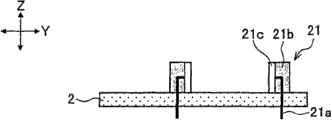
以下使用附图说明本发明的一实施方式。图1(a)是示出本实施方式中的光传输模块1与基板2的连接状态的侧视图,图1(b)是其俯视图。One embodiment of the present invention will be described below using the drawings. FIG. 1( a ) is a side view showing the connection state of the
最初,使用图1(a)和图1(b)简单说明利用光传输模块1的数据通信的结构。这里,为使光传输模块1在设备(未作图示)内部进行数据通信,假定光传输模块1的一端搭载在基板2A上,光传输模块1的另一端搭载在基板2B上。First, the configuration of data communication using the
首先,光传输模块1接收通过基板2A传输来的电信号。然后,光传输模块1将接收到的电信号转换成光信号,将该光信号向基板2B方向传播,再次转换成电信号来传输到基板2B。First, the
这样,通过使光传输模块1和基板2电连接,可进行设备内部的基板间的数据通信。以下,说明光传输模块1和基板2的详细结构。另外,以下,考虑到搭载在小型薄型设备上的光传输模块,将光传输路作为光波导路进行说明,然而不限于此,光传输路可以是光纤等。In this way, by electrically connecting the
首先,说明各部分的结构。First, the configuration of each part will be described.
(光传输模块的结构)(Structure of Optical Transmission Module)
如图2所示,光传输模块1具有:光波导路(光传输路)11,收发光元件(光元件)12,接合线13,以及封装件(第1基板)14。As shown in FIG. 2 , the
光波导路11由折射率大的芯部11a和与该芯部11a的周围相接而设置的折射率小的包层部11b形成,并利用在该芯部11a和包层部11b的边界重复的全反射来传播已入射到芯部11a的光信号。由于芯部11a和包层部11b由具有柔性的高分子材料构成,因而光波导路11具有柔性。The
这里,简单说明光波导路11上的光信号的传播结构。Here, the propagation structure of the optical signal on the
如图2所示,光波导路11的端面被加工成45度的倾斜面,从光波导路11的射入射出口11c入射的光信号由一个端面反射,光路进行90度转换而被引导到光波导路11内。被引导到光波导路11内的光信号在其内部重复全反射的同时向另一个端面方向传播。然后,由另一个端面反射的光信号,其光路进行90度转换而从射入射出口11c向外部射出。As shown in FIG. 2, the end face of the
另外,本实施方式中的光波导路11的端面角度被加工成45度,然而不限于此,只要是能将光信号引导到光波导路11内的结构即可。因此,作为其他结构,例如可以是这样的结构,即:将光波导路11的端面加工成直角,从与该端面垂直的方向射入射出光信号。In addition, although the end face angle of the
收发光元件12将电信号转换成光信号或者将光信号转换成电信号。并且,收发光元件12是面收发光型的元件,从与搭载在后述的封装件14底板上的搭载面相反侧的面发送或接收光信号。The
接合线13将收发光元件12和设置在后述的封装件14上的电气配线(未作图示)连接来传递电信号。The
封装件14具有这样的结构,即:由从底板立起的侧壁形成为凹状以包围四周,并使用盖关闭上部的开口部。在封装件14的内部设置有上述的光波导路11的端部、收发光元件12以及接合线13。并且,封装件14具有与上述的电气配线(未作图示)和外部接触的电极(未作图示),并具有这样的结构,即:与外部例如基板电连接来通过接合线13将电信号传递到收发光元件12。另外,作为封装件14使用的材料,可选择环氧树脂、陶瓷、玻璃、塑料等各种材料。并且,在封装件14的内部可以搭载用于驱动收发光元件12的驱动电路、IC、IC的驱动电路等各种元件。The
另外,本实施方式中的封装件14如上所述具有形成为凹状以容纳光波导路11的端部和收发光元件12等的结构,然而不限于此,例如,可以是由搭载有光波导路11的端部和收发光元件12等的平板状的基板构成的结构。In addition, the
以下使用图2和图3说明由上述各部件构成的光传输模块1的制造方法的一例。另外,在图2和图3中,将封装件14的开口面14a上的平行于光波导路11长度方向的轴设定为Y轴,将垂直于Y轴的轴设定为X轴,将坐标平面设定为X-Y平面,将垂直于X-Y平面的轴设定为Z轴。An example of a method of manufacturing the
首先,在被夹具等固定的封装件14上,使用钎焊等的方法来预先安装收发光元件12、接合线13、电气配线(未作图示)、电连接部(未作图示)以及电极(未作图示)。然后,使用气动卡盘等来把持光波导路11,使用在封装件14的上方(Z轴方向)设置的图像识别装置(未作图示)来进行收发光元件12和光波导路11的位置调整。在光波导路11的倾斜端面上的芯部的投影部(射入射出口)11c和收发光元件12的射入射出部一致的位置,使用粘接等方法将光波导路11固定在封装件14的开口面14a上。First, on the
根据使用上述方法所制造的光传输模块1,由于可支撑光波导路11的射入射出口11c的周围,因而可将收发光元件12中的光信号的射入射出部与光波导路11中的光信号的射入射出口11c之间的距离以及两者的位置关系保持一定。因此,可抑制收发光元件12和光波导路11的光耦合效率的变动,可进行稳定的数据信号传输。According to the
另外,光波导路11的固定方法不作特别限定,只要能将收发光元件12与光波导路11中的光信号的射入射出口11c之间的距离以及两者的位置关系保持一定,就可以是其他结构。作为其他结构,例如可列举出将支撑光波导路11的端部的支撑部件安装在封装件14上的结构。In addition, the fixing method of the
(基板的结构)(substrate structure)
图4(a)是示出基板(第2基板)2的概略结构的侧视图,图4(b)是其俯视图。基板2是与设备(未作图示)连接的一般基板,搭载有各种元件,并在该元件间传递电信号。并且,在基板2上设置有用于保持光传输模块1的封装件14的弹性保持部(连接部件)21。FIG. 4( a ) is a side view showing a schematic structure of the substrate (second substrate) 2 , and FIG. 4( b ) is a plan view thereof. The
弹性保持部21具有:插入到基板2的贯通孔内的销(连接部、电极销)21a;保持光传输模块1的弹性部21b;以及设置在该弹性部21b上并与销21a电连接的电极21c。另外,弹性部21b由可吸收振动和冲击等的弹性材料构成,具体地说例如可列举出橡胶、弹簧、粘接薄板、树脂等的材料。并且,电极21c与在光传输模块1的封装件14上设置的电极接触,从而与收发光元件12电连接。上述弹性保持部21通过钎焊、电连接器(连接部)等电连接固定在基板2上。The elastic holding
下面,使用图1(a)和图1(b)以及图4(a)和图4(b)来说明光传输模块1和基板2中的电信号的通信结构。这里,以在基板2上搭载驱动IC的情况为例进行说明。Next, the communication structure of the electrical signal in the
搭载在一个基板2A上的驱动IC取得来自控制部(未作图示)的命令而发送电信号。所发送的电信号在基板2A内传播,并通过弹性保持部21的销21a被引导到电极21c,以用于将数据传输到另一基板2B。然后,上述电信号通过与电极21c接触的封装件14被输入到收发光元件(发光元件)12。输入到收发光元件12的电信号如上所述被转换成光信号并在光波导路11内传播。在光波导路11内传播的光信号由收发光元件(受光元件)12接收,再次被转换成电信号。然后,转换后的电信号通过封装件14被引导到与该封装件14接触的另一个弹性保持部21的电极21c,通过销21a被输入到搭载在另一个基板2B上的例如放大器等(未作图示),被放大到期望的输出。The driver ICs mounted on one
如上所述,通过将光传输模块1经由弹性保持部21与基板2电连接,从而可利用光传输进行数据通信。As described above, by electrically connecting the
以下说明光传输模块1和基板2的连接部的结构。另外,以下,将平行于基板2中的搭载弹性保持部21的面的坐标平面设定为X-Y平面,将垂直于X-Y平面的轴设定为Z轴,将平行于光波导路11的长度方向的轴设定为Y轴,将垂直于Y轴的轴设定为X轴。The structure of the connecting portion between the
图5(a)是示出在从基板2的上方(Z轴方向)嵌合光传输模块1的情况下的连接方法的侧视图,图5(b)是示出光传输模块1与基板2的连接状态的俯视图。FIG. 5( a ) is a side view showing a connection method in the case of fitting the
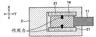
如图5(a)和图5(b)所示,在基板2上,通过钎焊等在Y轴方向上相对设置有一对弹性保持部21。并且,在一对弹性保持部21的相对面上设置有与封装件14电连接的电极21c。另外,电极21c可以设置在一对弹性保持部21内的任一方上。并且,优选的是,一对弹性保持部21之间的距离小于光传输模块1在封装件14中的Y轴方向的长度。即,优选的是,上述距离被调整成可使保持在一对弹性保持部21之间的封装件14移动到Y轴方向的+侧和-侧的程度。As shown in FIG. 5( a ) and FIG. 5( b ), on the
在上述结构中,如图5(a)所示从Z轴方向插入到一对弹性保持部21之间的光传输模块1,从一对弹性保持部21受到在Y轴方向相互不同方向的作用力。由此,可将光传输模块1保持在与基板2电连接的状态。然后,光传输模块1由于通过弹性保持部21而与基板2连接,因而可在被保持于一对弹性保持部21之间的状态下独立于基板2移动。In the above structure, the
因此,即使在基板2发生变形等的情况下,该影响也由弹性保持部21吸收,而不会传到光传输模块1。具体地说,例如在由于外力或热的影响而使基板2发生Z轴方向(上方)的翘曲的情况下,弹性保持部21在一对弹性保持部21沿Y轴方向相互离开的方向进行变形。然而,该变形只对从弹性保持部21赋予给光传输模块1的作用力产生影响,而不会给光传输模块1的封装件14的形状带来影响。由此,即使在安装有光传输模块1的基板2发生变形的情况下,也能防止光传输模块1的变形,因而可将光传输模块1的收发光元件12中的光信号的射入射出部与光波导路11中的光信号的射入射出口11c之间的距离和两者的位置关系保持一定。因此,不会使光耦合效率变动,可进行稳定的数据传输。Therefore, even if the
并且,在本实施方式中,在使光传输模块1与基板2连接时,由于不利用钎焊等的热,因而组装作业容易。而且,由于采用从侧面(X轴方向、Y轴方向)保持光传输模块1的封装件14的结构,因而与使用现有的电连接器的情况相比较,可使光传输模块1的连接部小型化和薄型化。In addition, in this embodiment, since heat such as soldering is not used when connecting the
另外,如图6(a)和图6(b)所示,可以在X轴方向相对设置一对弹性保持部21。这样,只要弹性保持部21在基板2上的固定位置是能配合封装件14的位置即可,可考虑与安装在基板2上的其他元件的配置来适当调整。In addition, as shown in FIG. 6( a ) and FIG. 6( b ), a pair of
并且,在上述说明中,采用了设置一对弹性保持部21并从两侧面保持光传输模块1的封装件14的结构,然而不限于此,可以设置至少一个弹性保持部21。在该情况下,如图7(a)和图7(b)所示,可采用在基板2上的与弹性保持部21相对的位置设置阶梯部2a并在该阶梯部2a与弹性保持部21之间嵌合封装件14的结构。阶梯部2a可以与基板2形成为一体,也可以采用作为单独部件来固定的结构。另外,优选的是,弹性保持部21具有朝阶梯部2a侧弯曲的形状,以便容易将封装件14插入两者之间。In addition, in the above description, a pair of elastic holding
并且,如图8(a)和图8(b)~图11(a)和图11(b)所示,可以采用在基板2上设置多个弹性保持部21以使光传输模块1与弹性保持部21的接点为3处以上的结构。由此,即使在光传输模块1受到基板2上的围绕Z轴的旋转方向θ的应力的情况下,该应力也由多个弹性保持部21吸收,不会传到光传输模块1。因此,可使光传输模块1更稳定。Moreover, as shown in FIG. 8(a) and FIG. 8(b) to FIG. 11(a) and FIG. The contact point of the holding
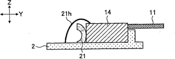
并且,如图12(a)和图12(b)所示,可以采用在弹性保持部21的Z轴方向的上部设置具有倾斜面的弹性的突起部21d的结构。由此,可容易将光传输模块1的封装件14插入到弹性保持部21间,并且所容纳的封装件14即使受到Z轴方向的应力,也难以从基板2脱开。因此,可更稳定地保持光传输模块1。另外,为了更稳定地保持光传输模块1,可以在封装件14的上表面设置用于容纳上述突起部21d的凹部14b。Furthermore, as shown in FIG. 12( a ) and FIG. 12( b ), a configuration may be adopted in which an
另外,在本实施方式中,采用将弹性保持部21设置在光传输模块1中的封装件14的侧面的结构,然而可以采用其他结构,例如将弹性保持部21设置在基板2与封装件14之间的结构。即,可以采用在搭载于基板2上的弹性保持部21的上表面(Z轴方向)搭载封装件14的结构。由此,即使在安装有光传输模块1的基板2发生变形的情况下,也能防止光传输模块1的变形。In addition, in this embodiment, the elastic holding
这里,如图13(a)和图13(b)所示,可以采用以对应于光传输模块1的封装件14的四角的方式在基板2上设置4处键状的弹性保持部21的结构。由此,在基板2上产生的各种方向的应力由四角的弹性保持部21吸收,不会传到光传输模块1。因此,可使光传输模块1更稳定。这样,在上述结构中,为了保持光传输模块1的四角,即使使各个弹性保持部21小型化,也能进行稳定的数据传输。因此,可将光传输模块1搭载在更小型的设备上。Here, as shown in FIG. 13(a) and FIG. 13(b), a structure in which four key-shaped elastic holding
并且,如图14(a)和图14(b)所示,可以采用在基板2上设置4处方柱状的弹性保持部21并在光传输模块1的封装件14的四角设置用于容纳弹性保持部21的Z轴方向的切口部(凹部)14c的结构。由此,可取得与图13(a)和图13(b)相同的效果。并且,由于容纳弹性保持部21的封装件14的外形尺寸可与图13(a)和图13(b)所示的封装件14的外形尺寸大致相同,因而可使模块整体更小型化。Moreover, as shown in Fig. 14(a) and Fig. 14(b), it is possible to set four-square columnar elastic holding
这里,在上述各结构中,采用将光传输模块1的封装件14从Z轴方向的上方插入到弹性保持部21之间的结构而作了说明,然而不限于此,可以采用从Y轴方向或X轴方向插入的结构。在该结构中,在层叠基板之间连接光传输模块1的情况下,或者在基板2的Z轴方向的上方没有空间的情况下是特别有效的。图15(a)和图15(b)以及图16(a)和图16(b)是上述结构的一例,也能应用于设置多个弹性保持部21的情况。Here, in each of the above-mentioned structures, a structure in which the
并且,如图17(a)和图17(b)所示,可以采用在光传输模块1中的封装件14的外壁设置凸部14d并在弹性保持部21的外壁设置容纳该凸部14d的凹部21e的结构。根据该结构,通过将封装件14的凸部14d插入到弹性保持部21的凹部21e内,可保持光传输模块1,因而可容易将光传输模块1插入到弹性保持部21之间,可提高组装作业的效率。另外,为了将光传输模块1和基板2电连接,优选的是在凹部21e内配备电极21c。并且,凸部14d在封装件14上的安装位置以及凹部21e在弹性保持部21上的安装位置不作特别限定,例如,如图18(a)和图18(b)所示,可以安装在Z轴方向的大致中间位置。Moreover, as shown in FIG. 17( a ) and FIG. 17( b ), it is possible to provide a
并且,如图19所示,可以在图17(a)和图17(b)中的封装件14外壁与凸部14d之间设置弹簧等的弹性部14e。Furthermore, as shown in FIG. 19 , an
另外,在本实施方式中,采用在将弹性保持部21预先通过钎焊等固定在基板2上之后安装光传输模块1的结构,然而不限于此,例如可以采用使光传输模块1的封装件14具有弹性保持部21并将弹性保持部21安装在基板2上的结构。并且,如图20(a)和图20(b)所示,可以采用在封装件14的两侧面(外壁面)设有保持部21b并将该封装件14插入到在基板2上相对设置的一对阶梯部2a和2b之间的结构。另外,在上述情况下,为了容易将封装件14插入到阶梯部2a和2b内,优选的是,保持部21b从封装件14向外部弯曲。由此,可将封装件14保持在基板2上,例如在基板2受到围绕Z轴的旋转方向θ的应力的情况下,该应力由弹性保持部21吸收,不会传到光传输模块1的封装件14。因此,光耦合效率不会变动,可进行稳定的数据传输。并且,由于采用保持封装件14的侧面(X轴方向、Y轴方向)的结构,并且由于可抑制Z轴方向的高度,因而可实现薄型化。In addition, in this embodiment, the structure in which the
并且,如图21(a)和图21(b)所示,可以采用这样的结构,即:在相对设置于基板2上的一对阶梯部2a、2b的内侧,以保持光传输模块1的封装件14侧面的方式将保持部21b插入在封装件14与阶梯部2a和/或阶梯部2b之间。由此,由于基板2的变形由保持部21吸收,因而可防止封装件14的变形。Furthermore, as shown in FIG. 21( a ) and FIG. 21( b ), such a structure may be adopted, that is, inside a pair of stepped
并且,如图22(a)和图22(b)所示,可以采用在使光传输模块1定位在基板2的期望位置之后将弹性保持部21安装在基板2上的结构。由此,由于可自由设定光传输模块1的搭载位置,因而可提高基板2上的安装效率。另外,如图23(a)和图23(b)所示,可以采用将平板状的弹性保持部21安装成从光传输模块1的封装件14的上方(Z轴方向)盖上的结构。由此,可自由设定光传输模块1的搭载位置,并且即使基板2发生Z轴方向的变形的情况下,也能进行更稳定的数据传输。Also, as shown in FIG. 22( a ) and FIG. 22( b ), a structure may be employed in which the elastic holding
这里,使用图24说明弹性保持部21的另一结构。图24是示出在将光传输模块1安装在弹性保持部21上的情况下的光传输模块1与基板2的连接方法的立体图。Here, another configuration of the elastic holding
如图24所示,弹性保持部21具有:对Z轴方向的上表面作了开口的形成为箱形状的壳体21f;设置在该壳体21f的外壁面且电连接固定在基板2上的销21a;以及设置在上述壳体21f内部且在4处保持光传输模块1的封装件14的由弹簧等构成的弹性部21b。并且,在弹性部21b中的与封装件14接触的位置设置有电极21c。另外,优选的是,壳体21f使用树脂一体成型。As shown in FIG. 24 , the elastic holding
并且,优选的是,如图24所示,在光传输模块1中的封装件14的外壁面上,沿Z轴方向具有容纳上述电极21c的槽部(凹部)14f。Furthermore, it is preferable that, as shown in FIG. 24 , on the outer wall surface of the
根据上述结构,通过将光传输模块1的封装件14嵌入到箱形状的弹性保持部21内就可进行安装,因而可提高安装作业的效率。并且,由于可以多个支点保持光传输模块1,因而可使光传输模块1更稳定,可进行稳定的数据传输。而且,由于弹性保持部21可进行一体的树脂成型,因而通用性优良,可实现成本降低。According to the above structure, since the
另外,在本实施方式中,采用将电极21c设置在弹性保持部21上的结构,然而不限于此,例如,如图25(a)和图25(b)所示,可以采用将金属线21g或柔性印刷基板(FPC)21h的一端与基板2连接并将另一端与光传输模块1的封装件14连接的结构。根据该结构,可不通过弹性保持部21而将基板2和光传输模块1电连接。并且,在该情况下,如图26所示,可以采用利用不包含电极的粘接薄板22作为弹性保持部21来将光传输模块1的封装件14与基板2连接的结构。In addition, in this embodiment, the
并且,作为图25(a)和图25(b)所示的弹性保持部21的变形例,弹性保持部21可以由设置在基板2上的弹性部21b以及与光传输模块1电连接的金属线21g或柔性印刷基板(FPC)21h构成。Moreover, as a modified example of the elastic holding
并且,如图27(a)和图27(b)所示,可以采用这样的结构,即:在光传输模块1中的封装件14的外壁设置了具有贯通孔14g的突起部14h,利用直径比该贯通孔14g的内部直径小的的固定销23来将封装件14与基板2连接。根据该结构,由于在固定销23与贯通孔14g之间形成间隙,因而封装件14可相对于基板2移动。因此,光传输模块1不会受到基板2发生的变形的影响。Furthermore, as shown in Fig. 27(a) and Fig. 27(b), such a structure may be adopted, that is, the outer wall of the
这里,本实施方式中的光传输模块1可与在基板2之间进行通信的电气配线(例如FPC21h)一起设置。在该情况下,优选的是,如图28所示,将光传输模块1的光波导路11的长度设定成比FPC21h的长度长。由此,即使在Y轴方向施加了力的情况下,由于不向光波导路11施加负荷,因而也能防止光波导路11的损伤,可进行稳定的数据传输。Here, the
图29(a)是示出图28所示的光传输模块的详细结构的图,图29(b)是沿图29(a)的A-A’线的剖视图,是示出在将封装件14插入到弹性保持部21之间的情况下的光传输模块1与基板2的连接方法的图。如图29(a)和图29(b)所示,光传输模块1由光波导路11、收发光元件12、封装件14、弹性保持部21以及第3基板24构成。Fig. 29(a) is a diagram showing the detailed structure of the optical transmission module shown in Fig. 28, and Fig. 29(b) is a cross-sectional view along line AA' of Fig. 29(a), showing that the
封装件14由搭载有收发光元件12的基板和从该基板立起的侧壁形成为凹部状,以将光波导路11和收发光元件12容纳在内部。收发光元件12具有将该收发光元件12的电端子24通过钎焊固定在上述基板上的结构。并且,采用上述基板和上述侧壁通过钎焊25a相互连接的结构。另外,在上述侧壁上设置有可进行与外部的电连接的电气配线26a。The
上述封装件14与第3基板24经由设置在封装件14的侧壁上的电气配线26a通过钎焊25b连接起来。这样,由于封装件14与第3基板24仅通过柔性电气配线26a来连接,因而因施加给第3基板24的振动、冲击、热膨胀、挠曲、拉伸、嵌合等作用所产生的应力难以传到封装件14。因此,收发光元件12和光波导路11难以受到第3基板24的变形的影响,因而不会使光耦合效率变动,可进行稳定的数据传输。The above-mentioned
弹性保持部21对置设置在基板2上,并具有电气配线26b,该电气配线26b是相互朝相对的方向实施作用力(图29(b)的黑箭头)的弹簧结构。根据该结构,如图29(b)所示,封装件14通过插入到相对的弹性保持部21之间(该图的白箭头方向)来固定在基板2上。由此,可将封装件14保持在电连接的状态。The
另外,优选的是,封装件14通过树脂成型来制作,其刚性大于第3基板24的刚性。并且,优选的是,第3基板24是FPC那样的具有柔性的基板。In addition, it is preferable that the
图30是示出在图29(b)所示的光传输模块中,在第3基板24和封装件14之间填充了树脂27的状态的图。FIG. 30 is a diagram showing a state where resin 27 is filled between
优选的是,填充的树脂27的弹性模量小于封装件14的弹性模量。由此,因施加给第3基板24的振动、冲击、热膨胀、挠曲、拉伸、嵌合等作用所产生的应力由树脂27吸收,因而难以传到封装件14。因此,收发光元件12和光波导路11难以受到第3基板24的变形的影响,因而不会使光耦合效率变动,可进行稳定的数据传输。Preferably, the elastic modulus of the filled resin 27 is smaller than that of the
并且,优选的是,树脂27的硬度大于封装件14的硬度。由此,第3基板24产生的上述应力由树脂27遮断,因而难以传到封装件14。因此,可取得与上述效果相同的效果。Also, it is preferable that the hardness of the resin 27 is greater than that of the
(应用例)(Application example)
最后,本实施方式的光传输模块1例如可以应用于以下的电子设备。Finally, the
首先,作为第一应用例,可用于折叠式便携电话、折叠式PHS(Personal Handyphone System,个人手机系统)、折叠式PDA(PersonalDigital Assistant,个人数字助理)、折叠式笔记本电脑等的折叠式电子设备中的铰链部中。First of all, as the first application example, it can be used in foldable electronic devices such as foldable mobile phones, foldable PHS (Personal Handyphone System), foldable PDA (Personal Digital Assistant), foldable notebook computers, etc. In the hinge part.
图31(a)~图31(c)示出将光传输模块1应用于折叠式便携电话40的例子。即,图31(a)是示出内置有光传输模块1的折叠式便携电话40的外观的立体图。FIGS. 31( a ) to 31 ( c ) show examples in which the
图31(b)是图31(a)所示的折叠式便携电话40中的应用光传输模块1的部分的框图。如该图所示,设置在折叠式便携电话40中的主体40a侧的控制部41与设置在以铰链部为轴可旋转地配备于主体一端的盖(驱动部)40b侧的外部存储器42、相机部(数码相机)43和显示部(液晶显示器显示)44分别通过光传输模块1连接。FIG. 31( b ) is a block diagram of a portion to which the
图31(c)是图31(a)中的铰链部(由虚线包围的部分)的透视俯视图。如该图所示,光传输模块1通过卷绕在铰链部中的支撑棒上进行弯曲,来分别连接在主体侧设置的控制部与在盖侧设置的外部存储器42、相机部43和显示部44。FIG. 31( c ) is a perspective top view of the hinge portion (portion surrounded by broken lines) in FIG. 31( a ). As shown in the figure, the
通过将光传输模块1应用于这些折叠式电子设备,可在有限的空间内实现高速大容量的通信。因此,例如特别适合于对折叠式液晶显示装置等的需要高速大容量的数据通信且要求小型化的设备。By applying the
作为第2应用例,光传输模块1可应用于打印装置(电子设备)中的打印机头和硬盘记录再现装置中的读取部等具有驱动部的装置中。As a second application example, the
图32(a)~图32(c)示出将光传输模块1应用于打印装置50的例子。图32(a)是示出打印装置50的外观的立体图。如该图所示,打印装置50具有在向纸52的宽度方向移动的同时对纸52进行打印的打印机头51,该打印机头51与光传输模块1的一端连接。FIGS. 32( a ) to 32 ( c ) show examples in which the
图32(b)是示出打印装置50中的应用光传输模块1的部分的框图。如该图所示,光传输模块1的一端部与打印机头51连接,另一端部与打印装置50中的主体侧基板连接。另外,该主体侧基板配备有控制打印装置50的各部分动作的控制单元等。FIG. 32( b ) is a block diagram showing a portion of the printing apparatus 50 to which the
图32(c)和图32(d)是示出在打印装置50中打印机头51移动(驱动)的情况下光传输模块1的光波导路11的弯曲状态的立体图。如该图所示,在将光传输模块1应用于打印机头51那样的驱动部的情况下,由于打印机头51的驱动而使光波导路11的弯曲状态发生变化,并且光波导路11的各位置反复弯曲。32( c ) and 32( d ) are perspective views showing the bent state of the
因此,本实施方式的光传输模块1适用于这些驱动部。并且,通过将光传输模块1应用于这些驱动部,可实现使用驱动部的高速大容量通信。Therefore, the
图33示出将光传输模块1应用于硬盘记录再现装置60的例子。FIG. 33 shows an example in which the
如该图所示,硬盘记录再现装置60具有磁盘(硬盘)61、机头(读取、写入用机头)62、基板导入部63、驱动部(驱动电动机)64以及光传输模块1。As shown in the figure, the hard disk recording and reproducing
驱动部64使机头62沿磁盘61的半径方向驱动。机头62读取记录在磁盘61上的信息,还在磁盘61上写入信息。另外,机头62通过光传输模块1与基板导入部63连接,将从磁盘61所读取的信息作为光信号传播到基板导入部63,并且接收从基板导入部63所传播的要写入到磁盘61内的信息的光信号。The driving
这样,通过将光传输模块1应用于硬盘记录再现装置60中的机头62那样的驱动部,可实现高速大容量通信。Thus, by applying the
本发明不限于上述实施方式,可在权利要求书所示范围内进行各种变更。即,将在权利要求书所示范围内作了适当变更后的技术手段进行组合而得到的实施方式也包含在本发明的技术范围内。The present invention is not limited to the above-described embodiments, and various changes can be made within the scope shown in the claims. That is, an embodiment obtained by combining technical means appropriately modified within the scope of the claims is also included in the technical scope of the present invention.
如上所述,本发明的连接部件优选的是,在上述记载的连接部件中,上述保持部设置在上述第2基板上。As described above, in the connecting member of the present invention, it is preferable that in the connecting member described above, the holding portion is provided on the second substrate.
根据上述结构,由于上述保持部设置在上述第2基板上,因而由第2基板保持的第1基板可相对于第2基板移动。因此,例如即使在由于外力和热的影响等而使第2基板发生翘曲等的变形的情况下,由于该变形量由保持部吸收,因而第1基板也不会发生变形。According to the above configuration, since the holding portion is provided on the second substrate, the first substrate held by the second substrate can move relative to the second substrate. Therefore, even if the second substrate is deformed such as warping due to, for example, external force or heat, the deformation amount is absorbed by the holding portion, so that the first substrate does not deform.
并且,本发明的连接部件优选的是,在上述记载的连接部件中,上述保持部保持如下所述的面,该面是上述第1基板中的与相对于连接上述连接部的上述第2基板面的面相交方向的面。In addition, in the connection member of the present invention, in the connection member described above, it is preferable that the holding portion holds a surface that is the surface of the first substrate that is opposite to the second substrate to which the connection portion is connected. Faces of Faces Faces in the direction of the face intersection.
根据上述结构,上述第1基板中的与相对于连接上述连接部的上述第2基板面的面相交方向的面由保持部保持。即,连接部件在第2基板与第1基板之间、或者在第1基板中的与对置于第2基板的面相反侧的面不连接,而与第1基板的侧面连接,因而可抑制与上述第2基板面垂直方向的高度,因此可使包含第2基板和第1基板的模块整体小型化和薄型化。According to the above configuration, the surface of the first substrate in a direction intersecting with the surface of the second substrate connected to the connecting portion is held by the holding portion. That is, the connection member is not connected between the second substrate and the first substrate, or on the surface of the first substrate opposite to the surface facing the second substrate, but is connected to the side surface of the first substrate, so that the Therefore, the overall height of the module including the second substrate and the first substrate can be reduced in size and thickness.
并且,本发明的连接部件优选的是,在上述记载的连接部件中,具有至少一对上述保持部,上述一对保持部对上述第1基板施加相反方向的作用力以保持该第1基板。In addition, the connection member of the present invention preferably has at least one pair of the holding portions in the connection member described above, and the pair of holding portions applies forces in opposite directions to the first substrate to hold the first substrate.
根据上述结构,上述第1基板是受到来自至少一对保持部的相反方向的作用力而被保持的。According to the above configuration, the first substrate is held by being biased in opposite directions from the at least one pair of holding portions.
由此,由于第1基板由弹性保持部保持成夹住该第1基板的侧面,因而例如即使在由于外力和热的影响等而使第2基板发生翘曲等的变形的情况下,该变形量由保持部吸收,因而第1基板也不会产生变形。因此,由于可将搭载在第1基板上的光元件和光波导路的位置关系保持一定,因而不会使光耦合效率变动,可进行稳定的数据传输。并且,由于保持第1基板的侧面,因而可使包含第2基板和第1基板的模块整体小型化和薄型化。As a result, since the first substrate is held by the elastic holding portion so as to sandwich the side surface of the first substrate, even when the second substrate is deformed such as warping due to external force or heat, for example, the deformation will not change. The amount is absorbed by the holding part, so the first substrate will not be deformed. Therefore, since the positional relationship between the optical element mounted on the first substrate and the optical waveguide can be kept constant, stable data transmission can be performed without changing the optical coupling efficiency. In addition, since the side surface of the first substrate is held, the entire module including the second substrate and the first substrate can be reduced in size and thickness.
并且,本发明的连接部件优选的是,在上述记载的连接部件中,上述连接部形成为凹部状以用于容纳上述第1基板,上述保持部设置在上述凹部中的面临内部空间的面上。In addition, in the connecting member of the present invention, in the connecting member described above, it is preferable that the connecting portion is formed in a concave shape for accommodating the first substrate, and the holding portion is provided on a surface of the concave portion facing the internal space. .
根据上述结构,上述第1基板在上述连接部的凹部内由弹性保持部保持成夹住该第1基板的侧面,因而可更稳定地保持第1基板,因此可进行更稳定的数据传输。并且,由于保持第1基板的侧面,因而可使包含第2基板和第1基板的模块整体小型化和薄型化。According to the above configuration, the first substrate is held by the elastic holding portion so as to sandwich the side surface of the first substrate in the concave portion of the connection portion, so that the first substrate can be held more stably, and thus more stable data transmission can be performed. In addition, since the side surface of the first substrate is held, the entire module including the second substrate and the first substrate can be reduced in size and thickness.
并且,本发明的连接部件优选的是,在上述记载的连接部件中,上述保持部在与上述第1基板相连接的连接位置具有电极。In addition, in the connection member of the present invention, in the connection member described above, it is preferable that the holding portion has an electrode at a connection position to the first substrate.
根据上述结构,由于上述保持部在与上述第1基板相连接的连接位置具有电极,因而即使在第1基板相对于第2基板移动的情况下,也能将第1基板保持在与电极连接的状态。因此,可进行稳定的数据传输。According to the above structure, since the holding part has an electrode at the connection position connected to the first substrate, even when the first substrate moves relative to the second substrate, the first substrate can be held at the position connected to the electrode. state. Therefore, stable data transmission can be performed.
并且,由于保持部具有电极,因而无需另行设置用于使第1基板和第2基板电连接的部件,因而可有效地利用第2基板上的空间,并可实现包含第2基板和第1基板的模块整体的小型化。In addition, since the holding part has electrodes, there is no need to separately provide components for electrically connecting the first substrate and the second substrate, so the space on the second substrate can be effectively used, and the combination of the second substrate and the first substrate can be realized. The overall miniaturization of the module.
并且,本发明的连接部件优选的是,在上述记载的连接部件中,上述连接部具有与上述第2基板电连接的电极销。Furthermore, in the connecting member of the present invention, it is preferable that in the connecting member described above, the connecting portion has an electrode pin electrically connected to the second substrate.
根据上述结构,由于上述连接部具有与上述第2基板电连接的电极销,因而可利用钎焊来与第2基板连接。并且,可通过电极销使第2基板和第1基板电连接。According to the above configuration, since the connecting portion has the electrode pins electrically connected to the second substrate, it can be connected to the second substrate by soldering. In addition, the second substrate and the first substrate can be electrically connected through electrode pins.
并且,本发明的光传输模块优选的是,在上述记载的光传输模块中,上述保持部设置在上述第1基板上。In addition, in the light transmission module of the present invention, it is preferable that in the light transmission module described above, the holding portion is provided on the first substrate.
由此,当连接了第1基板和第2基板时,由于具有弹性的保持部夹设在第1基板和第2基板之间,因而第1基板可相对于第2基板移动。由此,即使在由于例如外力和热的影响等而使第2基板发生翘曲等的变形的情况下,由于该变形量由保持部吸收,因而第1基板也不发生变形。Thus, when the first substrate and the second substrate are connected, since the elastic holding portion is interposed between the first substrate and the second substrate, the first substrate can move relative to the second substrate. Thereby, even if the second substrate is deformed by warping or the like due to, for example, external force or thermal influence, the first substrate is not deformed because the amount of deformation is absorbed by the holding portion.
并且,本发明的光传输模块优选的是,在上述记载的光传输模块中,上述第1基板设置有容纳上述连接部件的凹部。In addition, in the light transmission module of the present invention, it is preferable that in the light transmission module described above, the first substrate is provided with a concave portion for accommodating the connecting member.
根据上述结构,由于上述第1基板设置有容纳上述连接部件的凹部,因而与在第1基板上不设置凹部的情况相比较,可减小容纳连接部件的第1基板的外形尺寸。因此,可实现包含第2基板和光传输模块的模块整体的小型化。According to the above configuration, since the first substrate is provided with the recess for accommodating the connection member, the outer dimension of the first substrate for accommodating the connection member can be reduced compared to the case where no recess is provided on the first substrate. Therefore, it is possible to reduce the size of the entire module including the second substrate and the optical transmission module.
并且,本发明的光传输模块优选的是,在上述记载的光传输模块中,上述第1基板由底板和侧壁形成为凹状,该底板搭载有上述光元件,该侧壁从该底板立起以包围该光元件的周围,容纳上述连接部件的凹部设置在上述侧壁中的面临上述凹状的内部空间的面相反侧的面上。In addition, in the optical transmission module of the present invention, in the optical transmission module described above, the first substrate is preferably formed in a concave shape by a bottom plate and a side wall on which the optical element is mounted, and the side wall stands up from the bottom plate. A concave portion for accommodating the connecting member is provided on a surface of the side wall opposite to a surface facing the concave internal space so as to surround the optical element.
根据上述结构,容纳连接部件的凹部设置在从搭载有上述光元件的底板立起以包围该光元件的周围的侧壁中的面临凹状的内部空间的面相反侧的面上。According to the above configuration, the recess for accommodating the connecting member is provided on the surface opposite to the surface facing the concave internal space among the side walls rising from the bottom plate on which the optical element is mounted so as to surround the optical element.
由此,与在第1基板上不设置凹部的情况相比较,可减小容纳连接部件的第1基板的外形尺寸。因此,可实现包含第2基板和光传输模块的模块整体的小型化。This makes it possible to reduce the external dimensions of the first substrate that accommodates the connecting member, compared to the case where no recess is provided on the first substrate. Therefore, it is possible to reduce the size of the entire module including the second substrate and the optical transmission module.
并且,本发明的光传输模块优选的是,在上述记载的光传输模块中,上述连接部件具有电极以用于与上述第2基板电连接。In addition, in the light transmission module of the present invention, it is preferable that in the light transmission module described above, the connection member has an electrode for electrically connecting to the second substrate.
根据上述结构,上述连接部件具有电极以用于与上述第2基板电连接。因此,通过使连接部件与第2基板连接,可使光传输模块和第2基板电连接。因此,由于无需另行设置用于使光传输模块和第2基板电连接的部件,因而可有效地利用第2基板上的空间,并可实现包含第2基板和光传输模块的模块整体的小型化。According to the above configuration, the connecting member has electrodes for electrically connecting to the second substrate. Therefore, by connecting the connection member to the second substrate, the optical transmission module and the second substrate can be electrically connected. Therefore, since there is no need to separately provide components for electrically connecting the optical transmission module and the second substrate, the space on the second substrate can be effectively used, and the entire module including the second substrate and the optical transmission module can be downsized.
并且,本发明的光传输模块优选的是,在上述记载的光传输模块中,上述第1基板的挠曲刚性大于上述第2基板。In addition, in the light transmission module of the present invention, in the light transmission module described above, preferably, the flexural rigidity of the first substrate is greater than that of the second substrate.
根据上述结构,由于上述第1基板的挠曲刚性大于上述第2基板,因而即使在第2基板由于外力等的影响而发生变形的情况下,第1基板也难以发生变形。因此,可将光元件和光波导路的位置关系保持一定,因而不会使光耦合效率变动,可进行稳定的数据传输。According to the above configuration, since the flexural rigidity of the first substrate is greater than that of the second substrate, even when the second substrate is deformed due to external force or the like, the first substrate is hardly deformed. Therefore, since the positional relationship between the optical element and the optical waveguide can be kept constant, stable data transmission can be performed without changing the optical coupling efficiency.
在发明的详细说明中执行的具体实施方式或实施例使本发明的技术内容非常清楚,不应仅限于这种具体例进行狭义解释,可在本发明的精神和后面记载的权利要求书的范围内进行各种变更来实施。The specific implementation or examples implemented in the detailed description of the invention make the technical content of the present invention very clear, and should not be limited to this specific example for narrow interpretation, but can be within the spirit of the present invention and the scope of the claims described later Make various changes to implement.
由于可进行使用柔性光缆的稳定的数据传输,因而可用作便携电话、笔记本个人计算机、PDA(便携信息终端)、液晶电视、台式监视器、打印机、车载电装设备、服务器、路由器、试验机、其他民用设备和通用设备等的基板间的数据传输。Since stable data transmission using flexible optical cables is possible, it can be used as mobile phones, notebook personal computers, PDAs (portable information terminals), LCD TVs, desktop monitors, printers, automotive electrical equipment, servers, routers, testing machines , Data transmission between substrates of other civil equipment and general equipment.
Claims (12)
Applications Claiming Priority (3)
| Application Number | Priority Date | Filing Date | Title |
|---|---|---|---|
| JP112774/2006 | 2006-04-14 | ||
| JP2006112774 | 2006-04-14 | ||
| PCT/JP2007/058145 WO2007119814A1 (en) | 2006-04-14 | 2007-04-13 | Optical transmission module, connecting part, and electronic device having optical transmission module |
Publications (2)
| Publication Number | Publication Date |
|---|---|
| CN101421650A CN101421650A (en) | 2009-04-29 |
| CN101421650B true CN101421650B (en) | 2014-05-14 |
Family
ID=38609574
Family Applications (1)
| Application Number | Title | Priority Date | Filing Date |
|---|---|---|---|
| CN200780013147.2A Expired - Fee Related CN101421650B (en) | 2006-04-14 | 2007-04-13 | Optical transmission module, connecting part, and electronic device having optical transmission module |
Country Status (5)
| Country | Link |
|---|---|
| US (2) | US7865046B2 (en) |
| JP (1) | JP5309990B2 (en) |
| KR (1) | KR100996805B1 (en) |
| CN (1) | CN101421650B (en) |
| WO (1) | WO2007119814A1 (en) |
Families Citing this family (18)
| Publication number | Priority date | Publication date | Assignee | Title |
|---|---|---|---|---|
| EP1986027A4 (en) * | 2006-01-11 | 2012-01-04 | Omron Tateisi Electronics Co | Optical cable module and apparatus employing it |
| JP2008091365A (en) * | 2006-09-29 | 2008-04-17 | Matsushita Electric Works Ltd | Photoelectric converter, and electronic apparatus employing it |
| US7918611B2 (en) * | 2007-07-11 | 2011-04-05 | Emcore Corporation | Reconfiguration and protocol adaptation of optoelectronic modules and network components |
| JP5246534B2 (en) * | 2008-02-22 | 2013-07-24 | 独立行政法人産業技術総合研究所 | Optical module |
| JP5246535B2 (en) * | 2008-02-22 | 2013-07-24 | 独立行政法人産業技術総合研究所 | Optical module |
| JP2009198921A (en) * | 2008-02-22 | 2009-09-03 | National Institute Of Advanced Industrial & Technology | Optical module |
| JP5407829B2 (en) * | 2009-12-15 | 2014-02-05 | 住友ベークライト株式会社 | Opto-electric hybrid board, optical module, opto-electric hybrid board manufacturing method, and electronic apparatus |
| US20110206379A1 (en) * | 2010-02-25 | 2011-08-25 | International Business Machines Corporation | Opto-electronic module with improved low power, high speed electrical signal integrity |
| JP5556905B2 (en) * | 2011-01-13 | 2014-07-23 | 株式会社村田製作所 | connector |
| CN105974535B (en) | 2011-07-01 | 2022-05-27 | 申泰公司 | Transceiver and interface for IC package |
| US9419403B2 (en) | 2011-07-01 | 2016-08-16 | Samtec, Inc. | Transceiver system |
| KR101276508B1 (en) | 2011-12-09 | 2013-06-18 | 엘에스엠트론 주식회사 | Optical interconnection module |
| DE102012008996A1 (en) * | 2012-05-04 | 2013-11-07 | Amphenol-Tuchel Electronics Gmbh | Electrical coupling device for an optoelectronic component |
| JP6319759B2 (en) | 2013-04-18 | 2018-05-09 | 日東電工株式会社 | Opto-electric hybrid module |
| JP2015014641A (en) * | 2013-07-03 | 2015-01-22 | Seiオプティフロンティア株式会社 | Communication equipment |
| JP6034778B2 (en) * | 2013-12-26 | 2016-11-30 | インテル・コーポレーション | Input/Output (I/O) Devices |
| JP6400316B2 (en) * | 2014-03-27 | 2018-10-03 | 住友電工デバイス・イノベーション株式会社 | Optical device |
| TWI678568B (en) * | 2018-08-21 | 2019-12-01 | 傳承光電股份有限公司 | Optical transceiver device |
Citations (2)
| Publication number | Priority date | Publication date | Assignee | Title |
|---|---|---|---|---|
| CN2362208Y (en) * | 1998-12-28 | 2000-02-02 | 颜裕峰 | Crystal circuit socket for plugging bridge terminals |
| CN2488205Y (en) * | 2001-02-13 | 2002-04-24 | 蔡周旋 | Chip socket |
Family Cites Families (38)
| Publication number | Priority date | Publication date | Assignee | Title |
|---|---|---|---|---|
| JPH0224810A (en) | 1988-07-13 | 1990-01-26 | Hitachi Ltd | Manufacture of thin-film magnetic head |
| JP2528779Y2 (en) * | 1988-08-03 | 1997-03-12 | オムロン株式会社 | Optical components |
| US5532711A (en) * | 1991-09-27 | 1996-07-02 | Inwave Corporation | Lightweight display systems and methods for making and employing same |
| JP3225620B2 (en) | 1992-09-07 | 2001-11-05 | 住友電気工業株式会社 | Optical module |
| JPH0725112A (en) * | 1993-07-08 | 1995-01-27 | Canon Inc | Recording head wiring connection mechanism |
| US5500761A (en) * | 1994-01-27 | 1996-03-19 | At&T Corp. | Micromechanical modulator |
| US5717960A (en) * | 1995-09-06 | 1998-02-10 | Nikon Corporation | Image vibration correcting device |
| JPH1168254A (en) * | 1997-08-25 | 1999-03-09 | Hitachi Ltd | Optical module and method of manufacturing optical module |
| CN2365786Y (en) | 1998-10-09 | 2000-02-23 | 杨建军 | Electric mobile connecting socket |
| US6272276B1 (en) * | 1998-10-15 | 2001-08-07 | Lucent Technologies, Inc. | Device and method for retaining a laser module in an orientation suitable for testing and shipping |
| US6463190B1 (en) * | 1998-10-16 | 2002-10-08 | Japan Aviation Electronics Industry Limited | Optical switch and method of making the same |
| US6254435B1 (en) * | 1999-06-01 | 2001-07-03 | Molex Incorporated | Edge card connector for a printed circuit board |
| US6535663B1 (en) * | 1999-07-20 | 2003-03-18 | Memlink Ltd. | Microelectromechanical device with moving element |
| DE19951158A1 (en) * | 1999-10-25 | 2001-04-26 | Harting Automotive Gmbh & Co | Arrangement of optoelectric elements |
| JP2001337249A (en) * | 2000-05-24 | 2001-12-07 | Matsushita Electric Works Ltd | Receptacle for optical communication |
| JP2002286959A (en) * | 2000-12-28 | 2002-10-03 | Canon Inc | Semiconductor device, photoelectric fusion substrate, and method of manufacturing the same |
| US7183633B2 (en) * | 2001-03-01 | 2007-02-27 | Analog Devices Inc. | Optical cross-connect system |
| WO2003104868A1 (en) * | 2002-06-06 | 2003-12-18 | 富士通株式会社 | Optical module manufacturing method and optical module |
| US6912333B2 (en) * | 2002-06-21 | 2005-06-28 | Fujitsu Limited | Optical interconnection apparatus and interconnection module |
| WO2004015764A2 (en) * | 2002-08-08 | 2004-02-19 | Leedy Glenn J | Vertical system integration |
| US6711312B1 (en) * | 2002-12-20 | 2004-03-23 | General Electric Company | Integrated optoelectronic circuit and method of fabricating the same |
| JP3936925B2 (en) * | 2003-06-30 | 2007-06-27 | 日本オプネクスト株式会社 | Optical transmission module |
| JP4301963B2 (en) * | 2004-01-27 | 2009-07-22 | 三菱電機株式会社 | Optical / electrical batch connector |
| US7271461B2 (en) * | 2004-02-27 | 2007-09-18 | Banpil Photonics | Stackable optoelectronics chip-to-chip interconnects and method of manufacturing |
| JP2006042307A (en) | 2004-03-12 | 2006-02-09 | Matsushita Electric Ind Co Ltd | Portable device |
| JP2005321560A (en) | 2004-05-07 | 2005-11-17 | Fuji Xerox Co Ltd | Polymer optical waveguide module with light receiving/emitting element |
| US7521292B2 (en) * | 2004-06-04 | 2009-04-21 | The Board Of Trustees Of The University Of Illinois | Stretchable form of single crystal silicon for high performance electronics on rubber substrates |
| JP2006024454A (en) * | 2004-07-08 | 2006-01-26 | Fujitsu Ltd | Connector |
| JP2006091241A (en) * | 2004-09-22 | 2006-04-06 | Hitachi Cable Ltd | Opto-electric composite wiring component and electronic device using the same |
| JP4306590B2 (en) * | 2004-11-05 | 2009-08-05 | セイコーエプソン株式会社 | Electro-optical device and electronic apparatus |
| US7305156B2 (en) * | 2005-03-29 | 2007-12-04 | Intel Corporation | Optical sub-assembly |
| JP4446930B2 (en) * | 2005-05-24 | 2010-04-07 | ヒロセ電機株式会社 | Photoelectric composite connector |
| US7637149B2 (en) * | 2005-06-17 | 2009-12-29 | Georgia Tech Research Corporation | Integrated displacement sensors for probe microscopy and force spectroscopy |
| JP2007013761A (en) * | 2005-07-01 | 2007-01-18 | Fujitsu Ltd | Delay time adjusting device and optical receiver using the same |
| US7441447B2 (en) * | 2005-10-07 | 2008-10-28 | Georgia Tech Research Corporation | Methods of imaging in probe microscopy |
| US20070194225A1 (en) * | 2005-10-07 | 2007-08-23 | Zorn Miguel D | Coherent electron junction scanning probe interference microscope, nanomanipulator and spectrometer with assembler and DNA sequencing applications |
| US7395698B2 (en) * | 2005-10-25 | 2008-07-08 | Georgia Institute Of Technology | Three-dimensional nanoscale metrology using FIRAT probe |
| JP2010504571A (en) * | 2006-09-19 | 2010-02-12 | イビデン株式会社 | Optical interconnect device and manufacturing method thereof |
-
2007
- 2007-04-13 CN CN200780013147.2A patent/CN101421650B/en not_active Expired - Fee Related
- 2007-04-13 US US12/296,516 patent/US7865046B2/en not_active Expired - Fee Related
- 2007-04-13 WO PCT/JP2007/058145 patent/WO2007119814A1/en not_active Ceased
- 2007-04-13 KR KR1020087021990A patent/KR100996805B1/en not_active Expired - Fee Related
- 2007-04-13 JP JP2008511001A patent/JP5309990B2/en not_active Expired - Fee Related
-
2009
- 2009-09-28 US US12/568,146 patent/US8087834B2/en not_active Expired - Fee Related
Patent Citations (2)
| Publication number | Priority date | Publication date | Assignee | Title |
|---|---|---|---|---|
| CN2362208Y (en) * | 1998-12-28 | 2000-02-02 | 颜裕峰 | Crystal circuit socket for plugging bridge terminals |
| CN2488205Y (en) * | 2001-02-13 | 2002-04-24 | 蔡周旋 | Chip socket |
Non-Patent Citations (1)
| Title |
|---|
| JP特开平11-68254A 1999.03.09 |
Also Published As
| Publication number | Publication date |
|---|---|
| US20090175579A1 (en) | 2009-07-09 |
| KR20080094098A (en) | 2008-10-22 |
| US8087834B2 (en) | 2012-01-03 |
| KR100996805B1 (en) | 2010-11-25 |
| US20100054672A1 (en) | 2010-03-04 |
| CN101421650A (en) | 2009-04-29 |
| JP5309990B2 (en) | 2013-10-09 |
| JPWO2007119814A1 (en) | 2009-08-27 |
| WO2007119814A1 (en) | 2007-10-25 |
| US7865046B2 (en) | 2011-01-04 |
Similar Documents
| Publication | Publication Date | Title |
|---|---|---|
| CN101421650B (en) | Optical transmission module, connecting part, and electronic device having optical transmission module | |
| CN101765794B (en) | Film light guide package, film light guide module, and electronic device | |
| JP5076603B2 (en) | Optical cable module and electronic device including optical cable module | |
| JP5170080B2 (en) | Package manufacturing method, package, and optical module | |
| JP5233990B2 (en) | Optical waveguide, optical waveguide module, and electronic device | |
| KR101077729B1 (en) | Light transmission path package, light transmission module, electronic device and method for manufacturing light transmission module | |
| JP2009169026A (en) | Optical transmission module, electronic device, and manufacturing method of optical transmission module | |
| KR101082730B1 (en) | Optical transmission module, electronic device, method for assembling optical transmission module and optical transmission method | |
| WO2009087882A1 (en) | Optical transmission module provided with reinforcing component for reinforcing substrate of optical transmission module, and electronic device provided with the optical transmission module | |
| JP4645651B2 (en) | Optical module | |
| JP5135804B2 (en) | Film optical waveguide, film optical waveguide module, and electronic device |
Legal Events
| Date | Code | Title | Description |
|---|---|---|---|
| C06 | Publication | ||
| PB01 | Publication | ||
| C10 | Entry into substantive examination | ||
| SE01 | Entry into force of request for substantive examination | ||
| C14 | Grant of patent or utility model | ||
| GR01 | Patent grant | ||
| CF01 | Termination of patent right due to non-payment of annual fee |
Granted publication date: 20140514 Termination date: 20170413 |
|
| CF01 | Termination of patent right due to non-payment of annual fee |