CN101401187A - Techniques for Monitoring and Controlling Plasma Manufacturing Processes - Google Patents
Techniques for Monitoring and Controlling Plasma Manufacturing Processes Download PDFInfo
- Publication number
- CN101401187A CN101401187A CNA2007800082052A CN200780008205A CN101401187A CN 101401187 A CN101401187 A CN 101401187A CN A2007800082052 A CNA2007800082052 A CN A2007800082052A CN 200780008205 A CN200780008205 A CN 200780008205A CN 101401187 A CN101401187 A CN 101401187A
- Authority
- CN
- China
- Prior art keywords
- plasma
- time
- ion
- ions
- ion species
- Prior art date
- Legal status (The legal status is an assumption and is not a legal conclusion. Google has not performed a legal analysis and makes no representation as to the accuracy of the status listed.)
- Granted
Links
Images


Classifications
-
- H—ELECTRICITY
- H01—ELECTRIC ELEMENTS
- H01J—ELECTRIC DISCHARGE TUBES OR DISCHARGE LAMPS
- H01J49/00—Particle spectrometers or separator tubes
- H01J49/26—Mass spectrometers or separator tubes
- H01J49/34—Dynamic spectrometers
- H01J49/40—Time-of-flight spectrometers
-
- H—ELECTRICITY
- H01—ELECTRIC ELEMENTS
- H01J—ELECTRIC DISCHARGE TUBES OR DISCHARGE LAMPS
- H01J37/00—Discharge tubes with provision for introducing objects or material to be exposed to the discharge, e.g. for the purpose of examination or processing thereof
- H01J37/32—Gas-filled discharge tubes
- H01J37/32917—Plasma diagnostics
- H01J37/32935—Monitoring and controlling tubes by information coming from the object and/or discharge
Landscapes
- Chemical & Material Sciences (AREA)
- Analytical Chemistry (AREA)
- Physics & Mathematics (AREA)
- Engineering & Computer Science (AREA)
- Plasma & Fusion (AREA)
- Other Investigation Or Analysis Of Materials By Electrical Means (AREA)
- Plasma Technology (AREA)
Abstract
Description
技术领域 technical field
本发明是关于一种监测和控制等离子体制造工艺的技术。The present invention relates to a technique for monitoring and controlling a plasma manufacturing process.
背景技术 Background technique
等离子体制造工艺广泛用于(例如)半导体制造,以使用各种掺杂剂对晶圆进行植入,以沉积或蚀刻薄膜。为了获得可预测以及可重复的制造工艺结果,其关键为严密监测和控制等离子体特征。举例而言,对等离子体掺杂(Plasma Doping,即PLAD)制造工艺的研究已表明等离子体的离子组成可能是一种判定掺杂剂种类、掺杂剂深度分布、制造工艺相关的污染等的关键信息。离子组成随PLAD制造工艺参数(诸如气体比例、总气压以及放电功率)而改变。视等离子体腔室的调节状态而定,离子组成亦可发生显著改变。因此,重要的是在PLAD制造工艺期间(较佳为当场(in-situ)及即时地)了解离子组成,以便获得可重复以及可预测的制造工艺结果。Plasma fabrication processes are widely used, for example, in semiconductor fabrication to implant wafers with various dopants to deposit or etch thin films. Close monitoring and control of plasma characteristics is critical for predictable and repeatable manufacturing process results. For example, research on the plasma doping (PLAD) manufacturing process has shown that the ion composition of the plasma may be a key to determine the type of dopant, the depth distribution of the dopant, the contamination related to the manufacturing process, etc. Key Information. Ion composition varies with PLAD fabrication process parameters such as gas ratio, total gas pressure, and discharge power. Depending on the tuning state of the plasma chamber, the ion composition can also change significantly. Therefore, it is important to know the ion composition during the PLAD fabrication process, preferably in-situ and in real time, in order to obtain repeatable and predictable fabrication process results.
现有等离子体工具往往缺乏提供等离子体的详细的即时信息(例如离子组成)的能力。举例而言,在典型PLAD制造工艺中,藉由基于法拉第杯(cup)电流监测植入剂量来控制等离子体。然而,法拉第杯仅为总电荷计数器,其并不区分不同的带电粒子或提供对等离子体特性的任何了解。尽管在一些传统束流(beam-line)离子植入系统中采用了当场质量分析,但在基于等离子体的离子植入系统中通常要避免使用当场质量分析,以便获得高产量。Existing plasma tools often lack the ability to provide detailed real-time information about the plasma, such as ion composition. For example, in a typical PLAD fabrication process, the plasma is controlled by monitoring implant dose based on Faraday cup current. However, the Faraday cup is only a total charge counter, which does not distinguish between different charged particles or provide any insight into the properties of the plasma. While in-situ mass analysis is employed in some conventional beam-line ion implantation systems, in-situ mass analysis is generally avoided in plasma-based ion implantation systems in order to achieve high throughput.
此外,现有习知离子感测器,诸如工业用质能分析器以及四极质谱仪,往往体积太大及/或太麻烦而不能在制造工具中实施。大型离子感测器倾向于扰动量测中的等离子体,且因此歪曲制造工艺结果。此外,现有习知离子感测器的尺寸以及重量往往限制其在半导体制造工艺工具中的部署选择可能。此外,在等离子体交替处于接通及关闭状态的脉冲等离子体处理中,往往需要对等离子体的时间解析的量测。然而,现有离子感测器很少提供时间解析的量测的能力。Additionally, existing conventional ion sensors, such as industrial mass analyzers and quadrupole mass spectrometers, are often too bulky and/or cumbersome to implement in manufacturing tools. Large ion sensors tend to perturb the plasma under measurement and thus skew the fabrication process results. In addition, the size and weight of conventional ion sensors often limit their deployment options in semiconductor manufacturing process tools. In addition, in pulsed plasma processing where the plasma is alternately on and off, time-resolved measurements of the plasma are often required. However, few existing ion sensors provide time-resolved measurement capability.
附图说明 Description of drawings
为了促进更全面地了解本发明,现参照随附图式,其中相同元件具有相同的参考数字。不应将该等图式视为对本发明的限制,而其仅意欲作为例示。To facilitate a more complete understanding of the present invention, reference is now made to the accompanying drawings, in which like elements bear like reference numerals. These drawings should not be considered as limitations of the invention, but are intended as illustrations only.
图1展示根据本发明的一实施例的例示性离子感测器。Figure 1 shows an exemplary ion sensor according to an embodiment of the invention.
图2展示具有一根据本发明的一实施例的例示性配置的离子感测器。Figure 2 shows an ion sensor with an exemplary configuration according to an embodiment of the invention.
图2a展示具有根据本发明的一实施例的能量分析器的离子感测器。Figure 2a shows an ion sensor with an energy analyzer according to an embodiment of the invention.
图3展示具有根据本发明的一实施例的另一例示性配置的离子感测器。Figure 3 shows an ion sensor with another exemplary configuration according to an embodiment of the invention.
图4展示具有根据本发明的一实施例的又一例示性配置的离子感测器。Figure 4 shows an ion sensor having yet another exemplary configuration according to an embodiment of the invention.
图5展示根据本发明的一实施例的离子感测器的一安装选项。FIG. 5 shows a mounting option for an ion sensor according to an embodiment of the invention.
图6展示根据本发明的一实施例的离子感测器的另一安装选项。Figure 6 shows another mounting option for an ion sensor according to an embodiment of the invention.
图6a至6c展示根据本发明的实施例的等离子体处理腔室的不同实例。Figures 6a to 6c show different examples of plasma processing chambers according to embodiments of the invention.
图7展示根据本发明的一实施例的离子感测器的又一安装选项。Figure 7 shows yet another mounting option for an ion sensor according to an embodiment of the invention.
图7a至图7b展示根据本发明的实施例的采用离子感测器以进行制造工艺式控制的例示性系统。7a-7b show an exemplary system employing ion sensors for manufacturing process control according to an embodiment of the present invention.
图8展示根据本发明的一实施例的例示性离子感测器。Figure 8 shows an exemplary ion sensor according to an embodiment of the invention.
50:等离子体 100:离子感测器50: plasma 100: ion sensor
101:电离源 102:外壳101: Ionization source 102: Shell
104:漂移管 106:提取器电极104: Drift tube 106: Extractor electrode
108:静电透镜 110:静电透镜108: Electrostatic lens 110: Electrostatic lens
112:侦测器总成 118:前置放大器112: Detector assembly 118: Preamplifier
120:电子介面 122:处理器单元120: Electronic interface 122: Processor unit
124:网格 200A:离子感测器124: grid 200A: ion sensor
300:离子感测器 400:离子感测器300: ion sensor 400: ion sensor
500:等离子体腔室 502:压板/阴极500: plasma chamber 502: platen/cathode
504:晶圆 506:阳极504: Wafer 506: Anode
507:阳极轴 508:离子感测器507: Anode shaft 508: Ion sensor
600A:等离子体腔室 600B:等离子体腔室600A:
600C:等离子体腔室 602:离子感测器600C: Plasma chamber 602: Ion sensor
604:波纹管密封部分 605:RF电源604: Bellows sealing part 605: RF power supply
606:RF线圈 607:RF匹配单元606: RF coil 607: RF matching unit
608:微波空腔 609:介电质介面608: Microwave cavity 609: Dielectric interface
611:微波源 613:调谐器611: microwave source 613: tuner
702:离子感测器 704:法拉第杯702: Ion Sensor 704: Faraday Cup
706:单元 708:电荷计数器706: Unit 708: Charge Counter
710:校正模块 712:系统控制器710: Calibration module 712: System controller
714:输出功能 800:离子感测器714: output function 800: ion sensor
具体实施方式 Detailed ways
现将参照如随附图式中所示的本发明的例示性实施例来更详细地描述本发明。虽然在下文中参照例示性实施例来描述本发明,但应了解本发明并不限于所述例示性实施例。已阅读本文中的教示的一般熟习此技艺者应了解属于本文中描述的本发明的范畴且本发明对于其具有显著应用价值的额外实施、变更、实施例以及其他使用领域。The present invention will now be described in more detail with reference to illustrative embodiments of the invention as shown in the accompanying drawings. While the invention is described hereinafter with reference to exemplary embodiments, it is to be understood that the invention is not limited to the exemplary embodiments. Those of ordinary skill in the art who have read the teachings herein will recognize additional implementations, permutations, embodiments, and other areas of use that fall within the scope of the invention described herein and to which the invention has significant application.
本发明的实施例提供许多适用于等离子体制造工艺的当场监测和控制的飞行时间(TOF)离子感测器的小型设计。该等设计可采用灵活的离子提取以及离子聚焦技术,以量测等离子体腔室中的离子组成。各TOF离子感测器可以各种方式安装于等离子体腔室中,且可被配置用于许多功能,诸如当场制造工艺式控制、腔室准备就绪验证、故障侦测、植入剂量校正以及植入均一性量测。各离子感测器的敏感性以及尺寸可允许对等离子体的时间解析量测以及空间量测。Embodiments of the present invention provide a number of compact designs of time-of-flight (TOF) ion sensors suitable for in-situ monitoring and control of plasma fabrication processes. These designs enable flexible ion extraction and ion focusing techniques to measure the ion composition in the plasma chamber. Each TOF ion sensor can be mounted in a plasma chamber in various ways and can be configured for many functions such as in situ process control, chamber readiness verification, fault detection, implant dose correction, and implant Uniformity measurement. The sensitivity and size of each ion sensor may allow time-resolved and spatial measurements of the plasma.
参看图1,其展示根据本发明的一实施例的例示性离子感测器100。在一些实施例中,离子感测器100包括产生接近离子感测器100的入口的离子的电离源101。在一实施例中,离子源101使用低能量电子源产生电子云。电子云中的电子会导致有助于中性原子及分子的电离的电子碰撞,以及藉由电子附着(attachment)而进行的离子转换。在各种其他实施例中,离子源101藉由离子碰撞电离及/或光子碰撞电离而产生接近离子感测器100的入口的离子。离子源101可为连续或脉冲离子源。离子源101对于一些需要提供对惰性气体或快速中性粒子种类(fast neutral species)的现有习知RGA型量测的应用是有用的。Referring to FIG. 1 , an
离子感测器100包含可经调适而安装于等离子体腔室的观察口中且可提供差动抽吸(differential pumping)的外壳102。外壳102可个别地偏压于所要电位Vhousing。可将外壳102的左手侧称为“提取器侧”,因为自等离子体提取的离子经由外壳102的左手侧上的小孔(“外壳小孔”)进入离子感测器100。可将外壳102的右手侧称为“侦测器侧”,因为离子侦测发生于外壳102的右手侧上。The
离子感测器100包括外壳102内部的漂移管104,所述漂移管亦可(例如)个别地以所要电位VL3进行偏压。漂移管104通常具有一具有可忽略的电磁场的空洞。漂移管104的提取器侧可具有用于接纳离子的小孔(“漂移管小孔”)。漂移管104的侦测器侧可具有允许离子退出,同时遮罩外部电场的网格(grid)124。等离子体腔室的压力通常为1毫托-3000毫托(mTorr),而漂移管压力通常为2×10⁻⁶托或更低。差动抽吸可用于维持压力差。
各种实施例包括一或多个电极及/或网格,其形成在外壳小孔与漂移管小孔之间接近漂移管104的提取器侧的透镜或偏转器。在一些实施例中,存在用于提取离子以及使离子聚焦的一连串电极。举例而言,可存在接近外壳小孔的提取器电极106。提取器电极106可具有直径在10微米与500微米(对于一些实施例,较佳为50-200微米)之间的小孔,尽管实际小孔尺寸可至少部分地根据差动抽吸的要求而改变。可以合适的电位Vextractor使提取器电极106偏压,以自等离子体吸引正离子或负离子。被吸引的离子可以不同角度行进。Various embodiments include one or more electrodes and/or grids that form lenses or deflectors near the extractor side of the
为了确保被吸引的离子在有限的射束角(例如等于或小于+/-1.5度)范围内向侦测器侧行进,可串联地配置两个或两个以上电极(例如静电透镜108及110),且使所述电极的小孔与外壳102、提取器106以及漂移管104的小孔对准。各静电透镜可个别地被偏压,以建立将离子导引于聚焦射束中的所要静电场。在各种操作模式中,静电透镜以正电压或负电压进行偏压。所述静电透镜之一可被提供电压脉冲以容许被吸引的离子的一部分(或组)进入漂移管104中。可以时控方式重复电压脉冲以实现周期性或近连续的离子取样。To ensure that the attracted ions travel toward the detector side within a limited range of beam angles (e.g., equal to or less than +/-1.5 degrees), two or more electrodes (e.g.,
在各种实施例中,将斥拒极(repeller)电压与提取电压脉冲的组合施加至任意电极对,以将正离子驱动至漂移管104中。相对于提取脉冲发生的时间而判定离子的飞行时间。举例而言,在一实施例中,以正电压脉冲VL1使静电透镜108偏压。正电压脉冲可为周期或非周期的。静电透镜110以正排斥电压VL2进行偏压。在一实施例中,将正斥拒极电压施加至静电透镜110,且将正电压脉冲施加至附近的静电透镜108,以便驱动正离子使通过斥拒极电极,以及进入漂移管104中。正斥拒极电压可为周期或非周期性的。当以VL3来偏压时,漂移管104可充当串联透镜中的第三静电透镜。漂移管上的偏压可为脉冲电压。使用类似配置,可将负离子提取至漂移管中。In various embodiments, a combination of repeller voltage and extraction voltage pulses are applied to any electrode pair to drive positive ions into the
在一些实施例中,将电压脉冲施加至所述电极中的一个以上的电极。举例而言,可将电压脉冲施加至漂移管104、提取器106、静电透镜108以及静电透镜110中的至少两者。可同时或延迟一预定时间而施加所述至少两电压脉冲,以便使离子进入漂移管。In some embodiments, voltage pulses are applied to more than one of the electrodes. For example, voltage pulses may be applied to at least two of
在一些实施例中,将阻隔电压施加至提取器106、静电透镜108、静电透镜110中的至少一个,以便有效地防止离子进入漂移管104。在一些操作方法中,周期性地使阻隔(blocking)电压的大小改变,以便允许一些离子进入漂移管。相对于此电压改变的时间而判定离子通过漂移管104的飞行时间。In some embodiments, a blocking voltage is applied to at least one of
一旦被接纳入漂移管104中,则离子实际上不受任何电场影响地向侦测器端漂移。离子通常具有相同的动能。重离子行进相对较慢,且轻离子行进相对较快。在给定充分的飞行时间(亦即漂移管104的充分长度)的情况下,离子基于其离子种类的离子质量而分离至个别组中。Once received into the
在一些实施例中,使用四极元件的配置来调变离子(正或负)经由漂移管的传输。在一实施例中,所述调变为周期性的。在另一实施例中,所述调变为非周期性的。可藉由改变与个别的四极元件关联的RF或DC电压来完成调变。在该等实施例中,相对于调变发生的时间而判定离子的飞行时间。In some embodiments, a configuration of quadrupole elements is used to modulate the transport of ions (positive or negative) through the drift tube. In an embodiment, the modulation is periodic. In another embodiment, the modulation is aperiodic. Modulation can be accomplished by varying the RF or DC voltages associated with individual quadrupole elements. In these embodiments, the time-of-flight of the ions is determined relative to the time at which the modulation occurs.
在各种其他实施例中,可藉由众多其他方法来调变离子(正或负)经由漂移管的传输。举例而言,可藉由对离子的静电偏转来调变所述离子传输。亦可藉由机械构件(诸如机械闸、多级切断装置或任何其他类型的机械断续器)来调变离子传输。举例而言,在一实施例中,机械断续器为机械闸门(shutter)。藉由机械构件进行的调变有时对于低能量应用是有利的。在该等实施例中,亦相对于调变发生的时间来判定离子的飞行时间。In various other embodiments, the transport of ions (positive or negative) through the drift tube can be modulated by numerous other methods. For example, the ion transport can be modulated by electrostatic deflection of ions. Ion transport can also be modulated by mechanical means such as mechanical gates, multi-stage cut-off devices, or any other type of mechanical interrupter. For example, in one embodiment, the mechanical interrupter is a mechanical shutter. Modulation by mechanical means is sometimes advantageous for low energy applications. In these embodiments, the time-of-flight of the ions is also determined relative to the time at which the modulation occurs.
在侦测器侧,侦测器总成(assembly)112可用于侦测离子。侦测器总成112可为任何类型的市售或定制的离子侦测装置(例如微通道板(MCP)总成)。例如可使用一或多个偏压(例如VMCP)来控制对离子的侦测及/或收集。侦测器总成112可耦接至前置放大器118,所述前置放大器又经由电子介面120耦接至处理器单元122。电子介面120(例如)可为快速数据撷取卡。处理器单元122(例如)可为个人电脑(PC)或工业型计算装置。On the detector side, a
具有截然不同的离子质量数的个别的离子组由侦测器依序侦测。已侦测的信号由前置放大器118放大。放大的信号然后由处理器单元122处理。对应于每一个别组的信号产生质谱中的质量峰值。基于对来自等离子体的离子种类的一个或多个取样,质谱精确地反映等离子体的离子组成。Individual ion groups with distinct ion masses are sequentially detected by the detector. The detected signal is amplified by the
在一些实施例中,侦测器总成112包括用于侦测在某些预定位置处的离子的位置敏感粒子侦测器。该等位置敏感粒子侦测器提供可用于判定离子质量或离子能量的离子位置信息。在各种实施例中,藉由电、磁或机械方法来选择用于侦测离子的侦测器表面的部分。举例而言,可藉由电性来定址的侦测器阵列可用于侦测离子以作为位置的函数。软件演算法可用于自侦测器信号撷取位置敏感数据。此外,可将机械构件用于控制撞击侦测器的离子的有效分散。举例而言,机械障壁(barrier)可用于遮罩侦测器的一部分。此外,可将离子偏转器或离子准直仪用于使离子偏转或成为准直,以使得离子仅撞击所要的侦测器部分。In some embodiments,
根据本发明的实施例,可藉由施加电位的不同组合至外壳102、漂移管104、提取器电极106、静电透镜108及110,以及侦测器总成112来灵活地配置离子感测器100。例示性组态显示在图2至图4中。According to embodiments of the present invention,
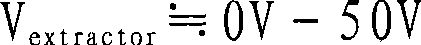
图2展示具有根据本发明的一实施例的一例示性组态的离子感测器200。离子感测器200可实质上包含与图1中所示的离子感测器100相同的组件。在该例示性组态中,可将外壳104接地及/或附着至等离子体腔室壁。在一些实施例中,将提取器电极106偏压于DC提取器电压

为了说明的目的,下文中的描述将假设仅获取正离子样本。然而,应注意的是可容易地调适或配置本发明的实施例以获取负离子样本。此外,为简单起见,将静电透镜108称为透镜1,静电透镜110称为透镜2,且将漂移管104称为透镜3。透镜1及透镜3可保持于相同或类似的电位,其可为在(例如)-150V与-300V之间的固定值。根据若干因数(诸如漂移管104的长度以及所要的离子质量解析度)来判定所要的电位。For purposes of illustration, the following description will assume that only positive ion samples are taken. It should be noted, however, that embodiments of the present invention can be readily adapted or configured to obtain negative ion samples. In addition, for simplicity, the
在一些实施例中,透镜1及透镜3可偏压于不同的电位(例如VL1=-400V--200V以及VL3=-200V)。透镜2可偏压于VL2=-500V--900V。可将透镜2更配置为用于漂移管104的“闸(gate)”。为了打开闸,可将短电压脉冲(例如50-500奈秒)提供至透镜2以将离子组(packet)接纳至漂移管104中。为了关闭闸,可将相对较大的正电位加于透镜2上,以阻挡正离子进入漂移管104。根据一实施例,通常可以正电压(例如+30V或以上)来偏压透镜2(亦即闸电极),在非常短的闸控周期期间除外。举例而言,假设闸脉冲宽度为100ns,且晶圆脉冲频率为5000kHz(周期=200微秒),且每一晶圆脉冲执行一次取样,则在所述周期(199.9微秒)的99.95%期间,闸电极关闭,且仅在所述周期的0.05%中,闸电极打开。In some embodiments, lens 1 and lens 3 can be biased at different potentials (eg, V L1 =-400V--200V and V L3 =-200V). The lens 2 can be biased at V L2 =-500V--900V. The lens 2 can be further configured as a "gate" for the
当闸脉冲与晶圆脉冲同步时,可引入延迟以控制相对于晶圆脉冲在何时打开闸脉冲。以此方式,有可能以高解析度在时间空间中的不同点处对等离子体进行取样。透镜1-3上的偏压的集合效应可为将接纳的离子聚焦于具有有限发散角的射束中的静电场。在侦测器侧,侦测器总成112可偏压于高电压VMCP。网格124可将漂移管104静电遮罩而隔离于所述高电压VMCP。When the gate pulse is synchronized with the wafer pulse, a delay can be introduced to control when the gate pulse is turned on relative to the wafer pulse. In this way, it is possible to sample the plasma at different points in space-time with high resolution. The collective effect of the bias voltages on lenses 1-3 can be an electrostatic field that focuses admitted ions into a beam with a finite divergence angle. On the detector side,
亦可配置离子感测器200以用于等离子体的时间解析量测。许多半导体处理等离子体为周期性地交替处于接通以及关闭(余辉)状态的“脉冲等离子体”。等离子体接通状态可持续每一循环的1-50%(或更高)。脉冲操作可导致等离子体状态以及制造工艺化学性质的动态改变。对离子种类的取样可与等离子体脉冲或晶圆偏压脉冲同步,或在所述两脉冲同步时,与所述两脉冲同步。藉由相对于参考脉冲(等离子体脉冲及/或晶圆偏压)来改变闸延迟,可在整个周期上进行时间解析量测。The ion sensor 200 can also be configured for time-resolved measurements of the plasma. Many semiconductor processing plasmas are "pulsed plasmas" that are periodically alternated on and off (afterglow) states. The plasma on state can last for 1-50% (or more) of each cycle. Pulsed operation can result in dynamic changes in the state of the plasma as well as in the chemistry of the fabrication process. Sampling of ion species may be synchronized with the plasma pulse or the wafer bias pulse, or with the two pulses when the two pulses are synchronized. By varying the gate delay relative to a reference pulse (plasma pulse and/or wafer bias), time-resolved measurements can be made over a period.
藉由观察开始信号与停止信号之间的时间差来判定离子的飞行时间。离子调变事件(电气或机械事件)由开始信号起始。停止信号由在离子侦测器处离子的到达时间来判定。在一些实施例中,将开始及停止信号用于闸控已知频率的脉冲串,以给出与飞行时间成比例的计数。在一特定实施例中,将开始及停止信号用于产生跨越电容器的电压,所述电容器然后以恒定速率放电。将所述放电周期用于闸控脉冲串,以给出与飞行时间成比例的计数。在另一实施例中,将开始及停止信号用来产生类比脉冲,其大小与飞行时间成比例。The time-of-flight of ions is determined by observing the time difference between the start signal and the stop signal. An ion modulation event (electrical or mechanical event) is initiated by a start signal. The stop signal is determined by the arrival time of the ions at the ion detector. In some embodiments, start and stop signals are used to gate a pulse train of known frequency to give a count proportional to flight time. In a particular embodiment, start and stop signals are used to generate a voltage across a capacitor, which is then discharged at a constant rate. The discharge cycle is used for gated bursts to give counts proportional to time-of-flight. In another embodiment, the start and stop signals are used to generate analog pulses whose magnitude is proportional to the time-of-flight.
离子感测器200亦可经配置以量测离子的能量分布及/或等离子体电位。在一实施例中,将电极或网格,诸如提取器电极106、静电透镜108以及静电透镜110经偏压以成为延迟元件。接着,量测作为电极电压的函数的所传输离子的数目。可自量测的数据来判定能量分布以及等离子体电位。Ion sensor 200 may also be configured to measure the energy distribution of ions and/or the plasma potential. In one embodiment, electrodes or grids, such as
在另一实施例中,藉由观察在侦测器总成122处离子的到达时间的散布来判定离子的能量分布。举例而言,可将位置敏感粒子侦测器用于侦测在某些预定位置处的离子,如结合图1所描述。此外,可藉由此项技术中众所熟知的方法来直接量测能量分布。举例而言,可将经校准的粒子侦测器用于藉由观察侦测器产生的信号的振幅来量测能量或质量。In another embodiment, the energy distribution of the ions is determined by observing the spread of the arrival times of the ions at the
在其他实施例中,漂移管104经配置以执行能量分析器的功能。存在众多将漂移管104配置为能量分析器的方法。举例而言,在一实施例中,漂移管104形成为曲线形状,且包括静电或磁偏转元件。漂移管104的形状经选择,使得具有不同能量的离子以不同角度转向。在另一实施例中,漂移管104包括作为至侦测器总成112的漂移路径的一部分的平行板能量分析器。举例而言,所述能量分析器可为45度型(45degree type)能量分析器。在另一实施例中,漂移管104包括作为至侦测器总成112的漂移路径的一部分的柱面镜或球面能量分析器。在另一实施例中,在离子路径中置放一或多个网格以将漂移管104配置为延迟电位元分析器。此外,在另一实施例中,漂移管可包括能够藉由调节RF或DC电压来区分具有不同能量的离子的RF四极或一个或多个永久磁铁或电磁铁。永久磁铁的位置可调整。In other embodiments, the
图2a展示具有根据本发明的一实施例的能量分析器114的离子感测器200A。能量分析器114定位于漂移管104与侦测器总成112之间。能量分析器114可用于选择所要能量范围中的离子。Figure 2a shows an ion sensor 200A with an energy analyzer 114 according to an embodiment of the invention. Energy analyzer 114 is positioned between
图3展示具有根据本发明的一实施例的另一例示性配置的离子感测器300。离子感测器300可实质上包含与图1中展示的离子感测器100相同的组件。然而,在该例示性配置中,提取器电极106接收RF(1-300MHz,通常为13.56MHz)偏压。RF偏压的提取器电极106可具有双重功能。亦即,提取器电极106可提取离子,且亦可在沉积为主的环境中自提取器小孔移除沉积物。FIG. 3 shows an
许多半导体制造工艺在沉积为主的环境中进行,其中薄膜材料沉积于等离子体腔室中。若厚绝缘膜阻塞提取器小孔,则提取器电极106上的DC偏压可能不再有效。RF偏压可有助于溅射清洗提取器小孔以移除沉积的材料。因此,RF偏压可向离子感测器300提供“自清洁”能力。对于离子提取,RF偏压可具有在-50V与0V之间的负平均电位(或RF自偏压),以及0V-100V的峰峰值。为了溅射清洗的目的,RF自偏压可大于溅射临限(threshold)值,且峰峰值可为100-1000V或更高。Many semiconductor manufacturing processes are performed in a deposition-based environment, where thin-film materials are deposited in plasma chambers. If a thick insulating film blocks the extractor aperture, the DC bias on the
图4展示具有根据本发明的一实施例的又一例示性配置的离子感测器400。离子感测器400可实质上包含与图1中展示的离子感测器100相同的组件。然而,在该例示性配置中,提取器电极106亦充当闸。可将闸脉冲提供至提取器电极106以将离子组拉入离子感测器400中。可向透镜2提供DC偏压以聚焦离子束。FIG. 4 shows an
为了灵活侦测等离子体腔室中的离子种类,可以许多方式安装根据本发明的实施例的离子感测器。例示性安装选项在图5至图7中展示。For flexible detection of ion species in a plasma chamber, ion sensors according to embodiments of the present invention can be installed in many ways. Exemplary mounting options are shown in Figures 5-7.
图5展示根据本发明的一实施例的离子感测器508的安装选项。展示了过于简化的等离子体腔室500,其具有固定晶圆504用的压板/阴极502。阳极506定位于压板/阴极502之上。阳极506未必须接地,但可偏压于例如在-1kV与+1kV之间的电压(可能为其他电压)。阳极轴507使得阳极506可在垂直方向上移动。等离子体50可藉由阴极偏压或藉由额外的等离子体源以产生于阳极506与压板/阴极502之间。FIG. 5 shows mounting options for an
对于离子植入应用,可将负电压脉冲施加至压板502以使正离子向晶圆504集合。对于负离子,可使用正电压脉冲。离子感测器508可安装于等离子体腔室500的侧壁中。所述安装可穿过观察口或类似机构。离子感测器508的提取器尖端可横向延伸至等离子体50的边缘中或附近。提取器尖端可定位于可移动的底座上。由于提取器尖端的尺寸小,因此可将其深深地插入等离子体50,而不会显著地干扰等离子体50。For ion implantation applications, negative voltage pulses may be applied to
图6展示根据本发明的一实施例的离子感测器的另一安装选项。在该安装选项中,替代或除了将离子感测器508安装于侧壁中以外,可将离子感测器602安装于阳极侧上。亦即,离子感测器602可穿过阳极506而定位,且可垂直地定向,使其提取器尖端向下伸到等离子体50上或伸至等离子体50中。离子感测器602可与阳极506电性连接。离子感测器602或其提取器尖端可独立于阳极506而向上及向下移动,以在等离子体腔室500中的不同空间点处获取离子样本。或者,离子感测器602或其提取器尖端可与阳极506一起向上及向下移动,以当场诊断不同制造工艺条件。可为了等离子体50的空间量测,以类似方式来致动水准地定位的离子感测器508。Figure 6 shows another mounting option for an ion sensor according to an embodiment of the invention. In this mounting option,
图6a至图6c展示根据本发明的实施例的等离子体处理腔室的不同实例。Figures 6a-6c show different examples of plasma processing chambers according to embodiments of the invention.
在图6a中,展示等离子体腔室600A。离子感测器602可穿过阳极506而安装着。波纹管密封部分604可提供离子感测器602穿过腔室壁的安装及移动。可藉由施加在晶圆504或压板502上的负脉冲电压来产生等离子体50。根据一实施例,自等离子体50将离子提取至离子感测器602中可与等离子体产生同步,且因此与晶圆504上的电压脉冲同步。In Fig. 6a, a
在图6b中,展示等离子体腔室600B。图6b中展示的等离子体产生技术不同于图6a中展示的等离子体产生技术。等离子体腔室600B可具有一个或多个外部等离子体源,例如ICP或Helicon等离子体源。举例而言,在一实施例中,将RF电源605以及RF匹配单元607耦接至RF线圈606。经由介电质介面609,RF线圈606可提供RF电力至等离子体腔室600B中。压板502可经偏压,以控制撞击晶圆504的离子的能量。In Fig. 6b, a
在图6c中,展示等离子体腔室600C,其中采用了另一等离子体产生技术。可将一个或多个微波发射源耦接至等离子体腔室600C以提供产生及维持等离子体50的功率。举例而言,可经由调谐器613以及波导或电缆将微波源611耦接至微波空腔608。供给至微波空腔608的微波功率可在其中产生“源等离子体”,因此,源等离子体可扩散至等离子体腔室600C中,以产生等离子体50。或者,藉由经由空腔608将微波功率耦接到等离子体腔室600C中而直接在等离子体腔室600C内部产生等离子体50。In Fig. 6c, a
图7展示根据本发明的一实施例的离子感测器的又一安装选项。在该安装选项中,可将一或多个离子感测器702安装于阴极侧上。亦即,离子感测器702可穿过压板/阴极502以垂直地定位着,使提取器尖端紧邻晶圆504而定位着。离子感测器702的安装位置可为(或靠近)法拉第杯通常所在的地方。因为提取器尖端向上指向等离子体50,所以离子感测器702以及晶圆504可相对于等离子体50以共用相同或类似的有利位置。因此,离子感测器702可“看见”与晶圆504所见相同的离子组成及剂量,此可有助于晶圆的等离子体处理的更精确的控制。在等离子体掺杂(PLAD)系统中,例如,离子感测器702可以直接侦测哪些离子已被植入至晶圆504中。若需要,亦可为了空间量测而向上及向下移动离子感测器702。Figure 7 shows yet another mounting option for an ion sensor according to an embodiment of the invention. In this installation option, one or
图7a至图7b展示根据本发明的实施例的采用离子感测器以进行制造工艺式控制的例示性系统。7a-7b show an exemplary system employing ion sensors for manufacturing process control according to an embodiment of the present invention.
图7a展示紧接于晶圆而安装的离子感测器702。可将法拉第杯704安装于晶圆504的另一侧上或法拉第杯704可部分地围绕晶圆504。离子感测器702及法拉第杯704和晶圆504一样向上面向等离子体(未图示)。可将离子感测器702耦接至单元706,其基于自离子感测器702接收的侦测数据而计算当场的离子组成。Figure 7a shows an
法拉第杯704可耦接至基于法拉第杯电流来计算总离子剂量的电荷计数器708。可将离子组成信息以及离子剂量数据输入至剂量校正模块710。此外,可将离子组成数据输入至系统控制器712以进行进一步的制造工艺式控制。The
图7b展示安装于晶圆504附近的两个或两个以上的离子感测器702。可将来自该等离子感测器702的当场离子组成数据输入至系统控制器712。系统控制器712的输出功能714可包括(但不限于)离子剂量校正、剂量均一性控制、等离子体腔室调节,及/或制造工艺故障侦测。在感测器安装于晶圆504周围的压板中的实施例中,漂移管104(图1)可与压板分离或处于压板电位。FIG. 7 b shows two or
对于等离子体50的阴极侧(或晶圆侧)量测,可与图2至图4中展示的离子感测器不同地配置离子感测器702。在图8中展示一实例。For cathode side (or wafer side) measurements of
图8展示根据本发明的一实施例的例示性离子感测器800。除移除了提取器电极106外,离子感测器800可实质上包含与图2中展示的离子感测器200相同的组件。提取器侧上的外壳小孔可收缩为大致10-500微米(较佳为50-200微米)。外壳102可被偏压于与晶圆504相同或类似的电位(例如0V--10kV)。透镜1、透镜3(漂移管104)以及侦测器总成112亦可被偏压于相同或类似的电位。透镜2可充当将离子组脉冲输送至漂移管104中的闸。FIG. 8 shows an
在此点上,应注意的是根据如上所述的本发明的离子感测器通常在某种程度上涉及输入数据的处理,以及输出数据的产生。在各种实施例中,可在硬件或软件中实施该输入数据处理以及输出数据产生。举例而言,可在等离子体处理工具或类似或相关的电路中采用特定的电子组件以实施与如上所述根据本发明的对离子种类的当场监测相关联的功能。或者,根据储存的指令来进行操作的一个或多个处理器可实施与如上所述根据本发明的对离子种类的当场监测相关联的功能。若情况如此,则此等指令储存于一个或多个处理器可读取的载体(例如磁盘)上或经由一个或多个信号传输至一个或多个处理器是属于本发明的范畴。At this point it should be noted that an ion sensor according to the invention as described above generally involves to some extent the processing of input data, as well as the generation of output data. In various embodiments, this input data processing and output data generation may be implemented in hardware or software. For example, specific electronic components may be employed in a plasma processing tool or similar or related circuitry to implement the functions associated with in situ monitoring of ion species according to the present invention as described above. Alternatively, one or more processors operating in accordance with stored instructions may implement the functions associated with in situ monitoring of ion species according to the present invention as described above. If this is the case, it is within the scope of the invention for such instructions to be stored on a carrier readable by one or more processors, such as a disk, or to be transmitted via one or more signals to one or more processors.
在一实施例中,可作为自动或半自动封闭控制环路的一部分而改变剂量或等离子体状态,所述封闭控制环路包括回应于自根据本发明的TOF感测器获得的数据的控制器或电脑以及电子仪器。自侦测器总成112获得的数据可包括经量测的TOF频谱的各个部分的绝对或相对大小。来自侦测器总成112的数据亦可包括飞行时间峰值的形状,例如FWHM的变化。来自侦测器总成112的数据亦可包括次要(污染物)峰值的存在与否、能量分布以及质量分布。In one embodiment, the dose or plasma state may be changed as part of an automatic or semi-automatic closed control loop comprising a controller or controller responsive to data obtained from a TOF sensor according to the present invention. Computers and electronic instruments. Data obtained from
来自TOF感测器的数据可用于侦测故障条件,诸如气体杂质、残余污染物以及用于控制等离子体的设备的故障。藉由调节TOF感测器的操作参数(诸如气体流量、气体混合物、压力、RF功率、RF频率、植入电压、工作循环或其他与等离子体相关的参数)可回应于所述数据而改变等离子体状态。Data from TOF sensors can be used to detect fault conditions such as gas impurities, residual contaminants, and malfunctions of equipment used to control the plasma. The plasma can be changed in response to the data by adjusting the TOF sensor's operating parameters such as gas flow, gas mixture, pressure, RF power, RF frequency, implant voltage, duty cycle, or other plasma related parameters. body state.
本发明的范畴并不受限于本文中描述的特定实施例。实际上,根据先前描述以及随附图式,本发明的其他各种实施例以及更改(除本文中描述的实施例以外)对于熟习此技艺者而言是显而易见的。因此,此等其他实施例以及更改仍属于本发明的范畴。此外,尽管是在为了特定目的的特定环境中的特定实施例的上下文中描述本发明,但熟习此技艺者应了解其实用性并不限于此,且本发明可有益地在用于许多目的的许多环境中实施。因此,应根据本文中描述的本发明的完整广度以及精神,来解译在下文中阐明的申请专利范围。The scope of the invention is not limited to the specific embodiments described herein. Indeed, various other embodiments and modifications of the invention, in addition to those described herein, will be apparent to those skilled in the art from the foregoing description and accompanying drawings. Therefore, these other embodiments and modifications still belong to the scope of the present invention. Furthermore, although the invention has been described in the context of a particular embodiment in a particular environment for a particular purpose, those skilled in the art will appreciate that its applicability is not limited thereto, and that the invention may be beneficially employed in many purposes. implemented in many environments. Accordingly, the claims set forth hereinafter should be construed in light of the full breadth and spirit of the invention described herein.
Claims (34)
Applications Claiming Priority (5)
| Application Number | Priority Date | Filing Date | Title |
|---|---|---|---|
| US11/371,907 | 2006-03-10 | ||
| US11/371,907 US7476849B2 (en) | 2006-03-10 | 2006-03-10 | Technique for monitoring and controlling a plasma process |
| US11/678,524 | 2007-02-23 | ||
| US11/678,524 US7453059B2 (en) | 2006-03-10 | 2007-02-23 | Technique for monitoring and controlling a plasma process |
| PCT/US2007/006244 WO2007106449A2 (en) | 2006-03-10 | 2007-03-09 | Technique for monitoring and controlling a plasma process |
Publications (2)
| Publication Number | Publication Date |
|---|---|
| CN101401187A true CN101401187A (en) | 2009-04-01 |
| CN101401187B CN101401187B (en) | 2012-05-30 |
Family
ID=38477985
Family Applications (1)
| Application Number | Title | Priority Date | Filing Date |
|---|---|---|---|
| CN2007800082052A Expired - Fee Related CN101401187B (en) | 2006-03-10 | 2007-03-09 | Technique for monitoring and controlling a plasma process |
Country Status (2)
| Country | Link |
|---|---|
| US (1) | US7476849B2 (en) |
| CN (1) | CN101401187B (en) |
Cited By (10)
| Publication number | Priority date | Publication date | Assignee | Title |
|---|---|---|---|---|
| CN102157324A (en) * | 2009-12-14 | 2011-08-17 | Spp处理技术系统英国有限公司 | Ion beam source |
| CN102290318A (en) * | 2011-07-01 | 2011-12-21 | 上海大学 | Proton transfer reaction device with multipole rod |
| CN103534780A (en) * | 2011-03-28 | 2014-01-22 | 东京毅力科创株式会社 | Ion energy analyzer, methods of electrical signaling therein, and methods of manufacturing and operating the same |
| CN104272103A (en) * | 2012-03-08 | 2015-01-07 | 陶氏益农公司 | Organocolloid-stabilized emulsions for control of insecticide spray drift |
| CN104584184A (en) * | 2012-07-13 | 2015-04-29 | 诺瓦工厂有限公司 | Assembly for use in a vacuum treatment process |
| CN104733279A (en) * | 2013-12-23 | 2015-06-24 | 中微半导体设备(上海)有限公司 | Plasma etching system |
| CN104733277B (en) * | 2013-12-23 | 2017-03-08 | 中微半导体设备(上海)有限公司 | Plasma etching system |
| CN106531603A (en) * | 2015-09-10 | 2017-03-22 | 台湾积体电路制造股份有限公司 | Ion collector, method for controlling plasma system, and method for processing substrate |
| CN108551828A (en) * | 2012-02-27 | 2018-09-21 | 阿吉齐科技公司 | The monitoring and control of edaphic condition |
| US12548745B2 (en) | 2024-05-03 | 2026-02-10 | Taiwan Semiconductor Manufacturing Company, Ltd. | Ion collector for use in plasma systems |
Families Citing this family (11)
| Publication number | Priority date | Publication date | Assignee | Title |
|---|---|---|---|---|
| US7531469B2 (en) * | 2004-10-23 | 2009-05-12 | Applied Materials, Inc. | Dosimetry using optical emission spectroscopy/residual gas analyzer in conjunction with ion current |
| US7453059B2 (en) * | 2006-03-10 | 2008-11-18 | Varian Semiconductor Equipment Associates, Inc. | Technique for monitoring and controlling a plasma process |
| US7476849B2 (en) * | 2006-03-10 | 2009-01-13 | Varian Semiconductor Equipment Associates, Inc. | Technique for monitoring and controlling a plasma process |
| US7714299B2 (en) * | 2006-08-08 | 2010-05-11 | Academia Sinica | Particle detector |
| US7888636B2 (en) * | 2007-11-01 | 2011-02-15 | Varian Semiconductor Equipment Associates, Inc. | Measuring energy contamination using time-of-flight techniques |
| US8097866B2 (en) * | 2008-02-14 | 2012-01-17 | Varian Semiconductor Equipment Associates, Inc. | Apparatus for measuring beam characteristics and a method thereof |
| US20100019141A1 (en) * | 2008-07-25 | 2010-01-28 | Varian Semiconductor Equipment Associates, Inc. | Energy contamination monitor with neutral current detection |
| US8698107B2 (en) | 2011-01-10 | 2014-04-15 | Varian Semiconductor Equipment Associates, Inc. | Technique and apparatus for monitoring ion mass, energy, and angle in processing systems |
| JP5722125B2 (en) * | 2011-06-03 | 2015-05-20 | 株式会社日立ハイテクノロジーズ | Mass spectrometer |
| DE102012200211A1 (en) * | 2012-01-09 | 2013-07-11 | Carl Zeiss Nts Gmbh | Device and method for surface treatment of a substrate |
| US10950421B2 (en) * | 2014-04-21 | 2021-03-16 | Lam Research Corporation | Using modeling for identifying a location of a fault in an RF transmission system for a plasma system |
Family Cites Families (25)
| Publication number | Priority date | Publication date | Assignee | Title |
|---|---|---|---|---|
| US3911314A (en) * | 1972-11-07 | 1975-10-07 | Strahlen Umweltforsch Gmbh | Ion gun for production of ion beams with particular radial current density profile |
| DE2947542A1 (en) | 1979-11-26 | 1981-06-04 | Leybold-Heraeus GmbH, 5000 Köln | DEVICE FOR MONITORING AND / OR CONTROLLING PLASMA PROCESSES |
| US5059739A (en) * | 1989-10-31 | 1991-10-22 | Exxon Chemical Patents Inc. | Hydrogen chloride-free catalyst system for dimerizing and codimerizing olefins |
| US5650616A (en) | 1992-04-14 | 1997-07-22 | Olympus Optical Co., Ltd. | Apparatus and method for analyzing surface |
| US5218204A (en) | 1992-05-27 | 1993-06-08 | Iowa State University Research Foundation, Inc. | Plasma sampling interface for inductively coupled plasma-mass spectrometry (ICP-MS) |
| US5784424A (en) | 1994-09-30 | 1998-07-21 | The United States Of America As Represented By The United States Department Of Energy | System for studying a sample of material using a heavy ion induced mass spectrometer source |
| US5614711A (en) * | 1995-05-04 | 1997-03-25 | Indiana University Foundation | Time-of-flight mass spectrometer |
| US5654543A (en) | 1995-11-02 | 1997-08-05 | Hewlett-Packard Company | Mass spectrometer and related method |
| US5905258A (en) * | 1997-06-02 | 1999-05-18 | Advanced Research & Techology Institute | Hybrid ion mobility and mass spectrometer |
| US6987264B1 (en) | 1998-01-23 | 2006-01-17 | Analytica Of Branford, Inc. | Mass spectrometry with multipole ion guides |
| GB9801565D0 (en) | 1998-01-23 | 1998-03-25 | Micromass Ltd | Method and apparatus for the correction of mass errors in time-of-flight mass spectrometry |
| US6101971A (en) * | 1998-05-13 | 2000-08-15 | Axcelis Technologies, Inc. | Ion implantation control using charge collection, optical emission spectroscopy and mass analysis |
| US6222186B1 (en) | 1998-06-25 | 2001-04-24 | Agilent Technologies, Inc. | Power-modulated inductively coupled plasma spectrometry |
| US6137112A (en) | 1998-09-10 | 2000-10-24 | Eaton Corporation | Time of flight energy measurement apparatus for an ion beam implanter |
| US6956205B2 (en) * | 2001-06-15 | 2005-10-18 | Bruker Daltonics, Inc. | Means and method for guiding ions in a mass spectrometer |
| US6946653B2 (en) * | 2001-11-27 | 2005-09-20 | Ciphergen Biosystems, Inc. | Methods and apparatus for improved laser desorption ionization tandem mass spectrometry |
| CN1639832B (en) | 2002-03-08 | 2010-05-26 | 美国瓦里安澳大利亚有限公司 | Plasma mass spectrometer |
| US7084393B2 (en) | 2002-11-27 | 2006-08-01 | Ionwerks, Inc. | Fast time-of-flight mass spectrometer with improved data acquisition system |
| US20040195503A1 (en) * | 2003-04-04 | 2004-10-07 | Taeman Kim | Ion guide for mass spectrometers |
| US7071466B2 (en) * | 2004-04-19 | 2006-07-04 | Ngx, Inc. | Mass spectrometry system for continuous control of environment |
| US7878145B2 (en) | 2004-06-02 | 2011-02-01 | Varian Semiconductor Equipment Associates, Inc. | Monitoring plasma ion implantation systems for fault detection and process control |
| GB0424426D0 (en) * | 2004-11-04 | 2004-12-08 | Micromass Ltd | Mass spectrometer |
| US7432516B2 (en) * | 2006-01-24 | 2008-10-07 | Brookhaven Science Associates, Llc | Rapid cycling medical synchrotron and beam delivery system |
| US7476849B2 (en) * | 2006-03-10 | 2009-01-13 | Varian Semiconductor Equipment Associates, Inc. | Technique for monitoring and controlling a plasma process |
| US7453059B2 (en) * | 2006-03-10 | 2008-11-18 | Varian Semiconductor Equipment Associates, Inc. | Technique for monitoring and controlling a plasma process |
-
2006
- 2006-03-10 US US11/371,907 patent/US7476849B2/en not_active Expired - Fee Related
-
2007
- 2007-03-09 CN CN2007800082052A patent/CN101401187B/en not_active Expired - Fee Related
Cited By (16)
| Publication number | Priority date | Publication date | Assignee | Title |
|---|---|---|---|---|
| CN102157324A (en) * | 2009-12-14 | 2011-08-17 | Spp处理技术系统英国有限公司 | Ion beam source |
| CN103534780A (en) * | 2011-03-28 | 2014-01-22 | 东京毅力科创株式会社 | Ion energy analyzer, methods of electrical signaling therein, and methods of manufacturing and operating the same |
| CN103534780B (en) * | 2011-03-28 | 2016-07-06 | 东京毅力科创株式会社 | Ion energy analysis instrument, in this ion energy analysis instrument the method for the method of electrical signal and manufacture and this ion energy analysis instrument of operation |
| CN102290318A (en) * | 2011-07-01 | 2011-12-21 | 上海大学 | Proton transfer reaction device with multipole rod |
| CN102290318B (en) * | 2011-07-01 | 2013-09-11 | 上海大学 | Proton transfer reaction device with multipole rod |
| CN108551828A (en) * | 2012-02-27 | 2018-09-21 | 阿吉齐科技公司 | The monitoring and control of edaphic condition |
| CN104272103A (en) * | 2012-03-08 | 2015-01-07 | 陶氏益农公司 | Organocolloid-stabilized emulsions for control of insecticide spray drift |
| CN104584184A (en) * | 2012-07-13 | 2015-04-29 | 诺瓦工厂有限公司 | Assembly for use in a vacuum treatment process |
| CN104733279B (en) * | 2013-12-23 | 2017-02-15 | 中微半导体设备(上海)有限公司 | Plasma etching system |
| CN104733277B (en) * | 2013-12-23 | 2017-03-08 | 中微半导体设备(上海)有限公司 | Plasma etching system |
| CN104733279A (en) * | 2013-12-23 | 2015-06-24 | 中微半导体设备(上海)有限公司 | Plasma etching system |
| CN106531603A (en) * | 2015-09-10 | 2017-03-22 | 台湾积体电路制造股份有限公司 | Ion collector, method for controlling plasma system, and method for processing substrate |
| US10553411B2 (en) | 2015-09-10 | 2020-02-04 | Taiwan Semiconductor Manufacturing Co., Ltd. | Ion collector for use in plasma systems |
| US11581169B2 (en) | 2015-09-10 | 2023-02-14 | Taiwan Semiconductor Manufacturing Co., Ltd. | Ion collector for use in plasma systems |
| US11996276B2 (en) | 2015-09-10 | 2024-05-28 | Taiwan Semiconductor Manufacturing Co., Ltd. | Ion collector for use in plasma systems |
| US12548745B2 (en) | 2024-05-03 | 2026-02-10 | Taiwan Semiconductor Manufacturing Company, Ltd. | Ion collector for use in plasma systems |
Also Published As
| Publication number | Publication date |
|---|---|
| US7476849B2 (en) | 2009-01-13 |
| US20070210248A1 (en) | 2007-09-13 |
| CN101401187B (en) | 2012-05-30 |
Similar Documents
| Publication | Publication Date | Title |
|---|---|---|
| CN101401187B (en) | Technique for monitoring and controlling a plasma process | |
| US7453059B2 (en) | Technique for monitoring and controlling a plasma process | |
| US8698107B2 (en) | Technique and apparatus for monitoring ion mass, energy, and angle in processing systems | |
| US7586100B2 (en) | Closed loop control and process optimization in plasma doping processes using a time of flight ion detector | |
| US20100159120A1 (en) | Plasma ion process uniformity monitor | |
| JP2009529765A5 (en) | ||
| GB2562990A (en) | Ion detector assembly | |
| CN102257606A (en) | Method and apparatus for plasma dose measurement | |
| US7888636B2 (en) | Measuring energy contamination using time-of-flight techniques | |
| WO2015175934A1 (en) | Deposition and patterning using emitted electrons | |
| CN103531432A (en) | Pulsed ion source, mass spectrometer and method for generating ions | |
| CN112868085B (en) | Ion detector | |
| EP1533828B1 (en) | Ion detector | |
| CN110739199B (en) | Method and system for detecting ion spatial distribution | |
| Budtz-Jorgensen | Studies of electrical plasma discharges | |
| JP7548156B2 (en) | Mass Spectrometer | |
| KR20140051123A (en) | Technique and apparatus for monitoring ion mass, energy, and angle in processing systems | |
| JPH11154485A (en) | Mass spectrograph and ion implantation device equipped with it | |
| JP2006221876A (en) | Ion detector, mass spectrometer having the same, and method for operating ion detector | |
| JP2022539216A (en) | Charged particle pulse generator and method for using the charged particle pulse generator |
Legal Events
| Date | Code | Title | Description |
|---|---|---|---|
| C06 | Publication | ||
| PB01 | Publication | ||
| C10 | Entry into substantive examination | ||
| SE01 | Entry into force of request for substantive examination | ||
| C14 | Grant of patent or utility model | ||
| GR01 | Patent grant | ||
| CF01 | Termination of patent right due to non-payment of annual fee | ||
| CF01 | Termination of patent right due to non-payment of annual fee |
Granted publication date: 20120530 Termination date: 20170309 |