CN101232042B - Light emitting device, method of manufacturing the same and manufacturing apparatus therefor - Google Patents
Light emitting device, method of manufacturing the same and manufacturing apparatus therefor Download PDFInfo
- Publication number
- CN101232042B CN101232042B CN2008100012874A CN200810001287A CN101232042B CN 101232042 B CN101232042 B CN 101232042B CN 2008100012874 A CN2008100012874 A CN 2008100012874A CN 200810001287 A CN200810001287 A CN 200810001287A CN 101232042 B CN101232042 B CN 101232042B
- Authority
- CN
- China
- Prior art keywords
- pixel electrode
- organic compound
- compound layer
- light emitting
- electrode
- Prior art date
- Legal status (The legal status is an assumption and is not a legal conclusion. Google has not performed a legal analysis and makes no representation as to the accuracy of the status listed.)
- Expired - Lifetime
Links
Images


Classifications
-
- H10P72/0468—
-
- H—ELECTRICITY
- H05—ELECTRIC TECHNIQUES NOT OTHERWISE PROVIDED FOR
- H05B—ELECTRIC HEATING; ELECTRIC LIGHT SOURCES NOT OTHERWISE PROVIDED FOR; CIRCUIT ARRANGEMENTS FOR ELECTRIC LIGHT SOURCES, IN GENERAL
- H05B33/00—Electroluminescent light sources
- H05B33/10—Apparatus or processes specially adapted to the manufacture of electroluminescent light sources
-
- H—ELECTRICITY
- H10—SEMICONDUCTOR DEVICES; ELECTRIC SOLID-STATE DEVICES NOT OTHERWISE PROVIDED FOR
- H10K—ORGANIC ELECTRIC SOLID-STATE DEVICES
- H10K50/00—Organic light-emitting devices
- H10K50/10—OLEDs or polymer light-emitting diodes [PLED]
- H10K50/11—OLEDs or polymer light-emitting diodes [PLED] characterised by the electroluminescent [EL] layers
- H10K50/125—OLEDs or polymer light-emitting diodes [PLED] characterised by the electroluminescent [EL] layers specially adapted for multicolour light emission, e.g. for emitting white light
- H10K50/13—OLEDs or polymer light-emitting diodes [PLED] characterised by the electroluminescent [EL] layers specially adapted for multicolour light emission, e.g. for emitting white light comprising stacked EL layers within one EL unit
-
- H—ELECTRICITY
- H10—SEMICONDUCTOR DEVICES; ELECTRIC SOLID-STATE DEVICES NOT OTHERWISE PROVIDED FOR
- H10K—ORGANIC ELECTRIC SOLID-STATE DEVICES
- H10K59/00—Integrated devices, or assemblies of multiple devices, comprising at least one organic light-emitting element covered by group H10K50/00
- H10K59/10—OLED displays
- H10K59/12—Active-matrix OLED [AMOLED] displays
- H10K59/123—Connection of the pixel electrodes to the thin film transistors [TFT]
-
- H—ELECTRICITY
- H10—SEMICONDUCTOR DEVICES; ELECTRIC SOLID-STATE DEVICES NOT OTHERWISE PROVIDED FOR
- H10K—ORGANIC ELECTRIC SOLID-STATE DEVICES
- H10K59/00—Integrated devices, or assemblies of multiple devices, comprising at least one organic light-emitting element covered by group H10K50/00
- H10K59/10—OLED displays
- H10K59/12—Active-matrix OLED [AMOLED] displays
- H10K59/124—Insulating layers formed between TFT elements and OLED elements
-
- H—ELECTRICITY
- H10—SEMICONDUCTOR DEVICES; ELECTRIC SOLID-STATE DEVICES NOT OTHERWISE PROVIDED FOR
- H10K—ORGANIC ELECTRIC SOLID-STATE DEVICES
- H10K59/00—Integrated devices, or assemblies of multiple devices, comprising at least one organic light-emitting element covered by group H10K50/00
- H10K59/30—Devices specially adapted for multicolour light emission
- H10K59/32—Stacked devices having two or more layers, each emitting at different wavelengths
-
- H—ELECTRICITY
- H10—SEMICONDUCTOR DEVICES; ELECTRIC SOLID-STATE DEVICES NOT OTHERWISE PROVIDED FOR
- H10K—ORGANIC ELECTRIC SOLID-STATE DEVICES
- H10K59/00—Integrated devices, or assemblies of multiple devices, comprising at least one organic light-emitting element covered by group H10K50/00
- H10K59/30—Devices specially adapted for multicolour light emission
- H10K59/35—Devices specially adapted for multicolour light emission comprising red-green-blue [RGB] subpixels
- H10K59/353—Devices specially adapted for multicolour light emission comprising red-green-blue [RGB] subpixels characterised by the geometrical arrangement of the RGB subpixels
-
- H—ELECTRICITY
- H10—SEMICONDUCTOR DEVICES; ELECTRIC SOLID-STATE DEVICES NOT OTHERWISE PROVIDED FOR
- H10K—ORGANIC ELECTRIC SOLID-STATE DEVICES
- H10K59/00—Integrated devices, or assemblies of multiple devices, comprising at least one organic light-emitting element covered by group H10K50/00
- H10K59/30—Devices specially adapted for multicolour light emission
- H10K59/38—Devices specially adapted for multicolour light emission comprising colour filters or colour changing media [CCM]
-
- H—ELECTRICITY
- H10—SEMICONDUCTOR DEVICES; ELECTRIC SOLID-STATE DEVICES NOT OTHERWISE PROVIDED FOR
- H10K—ORGANIC ELECTRIC SOLID-STATE DEVICES
- H10K59/00—Integrated devices, or assemblies of multiple devices, comprising at least one organic light-emitting element covered by group H10K50/00
- H10K59/80—Constructional details
- H10K59/8791—Arrangements for improving contrast, e.g. preventing reflection of ambient light
- H10K59/8792—Arrangements for improving contrast, e.g. preventing reflection of ambient light comprising light absorbing layers, e.g. black layers
-
- H—ELECTRICITY
- H10—SEMICONDUCTOR DEVICES; ELECTRIC SOLID-STATE DEVICES NOT OTHERWISE PROVIDED FOR
- H10K—ORGANIC ELECTRIC SOLID-STATE DEVICES
- H10K2102/00—Constructional details relating to the organic devices covered by this subclass
- H10K2102/301—Details of OLEDs
- H10K2102/302—Details of OLEDs of OLED structures
- H10K2102/3023—Direction of light emission
- H10K2102/3026—Top emission
-
- H—ELECTRICITY
- H10—SEMICONDUCTOR DEVICES; ELECTRIC SOLID-STATE DEVICES NOT OTHERWISE PROVIDED FOR
- H10K—ORGANIC ELECTRIC SOLID-STATE DEVICES
- H10K59/00—Integrated devices, or assemblies of multiple devices, comprising at least one organic light-emitting element covered by group H10K50/00
- H10K59/10—OLED displays
- H10K59/12—Active-matrix OLED [AMOLED] displays
-
- H—ELECTRICITY
- H10—SEMICONDUCTOR DEVICES; ELECTRIC SOLID-STATE DEVICES NOT OTHERWISE PROVIDED FOR
- H10K—ORGANIC ELECTRIC SOLID-STATE DEVICES
- H10K59/00—Integrated devices, or assemblies of multiple devices, comprising at least one organic light-emitting element covered by group H10K50/00
- H10K59/10—OLED displays
- H10K59/17—Passive-matrix OLED displays
-
- H—ELECTRICITY
- H10—SEMICONDUCTOR DEVICES; ELECTRIC SOLID-STATE DEVICES NOT OTHERWISE PROVIDED FOR
- H10K—ORGANIC ELECTRIC SOLID-STATE DEVICES
- H10K59/00—Integrated devices, or assemblies of multiple devices, comprising at least one organic light-emitting element covered by group H10K50/00
- H10K59/80—Constructional details
- H10K59/87—Passivation; Containers; Encapsulations
- H10K59/871—Self-supporting sealing arrangements
-
- H—ELECTRICITY
- H10—SEMICONDUCTOR DEVICES; ELECTRIC SOLID-STATE DEVICES NOT OTHERWISE PROVIDED FOR
- H10K—ORGANIC ELECTRIC SOLID-STATE DEVICES
- H10K59/00—Integrated devices, or assemblies of multiple devices, comprising at least one organic light-emitting element covered by group H10K50/00
- H10K59/80—Constructional details
- H10K59/87—Passivation; Containers; Encapsulations
- H10K59/873—Encapsulations
-
- H—ELECTRICITY
- H10—SEMICONDUCTOR DEVICES; ELECTRIC SOLID-STATE DEVICES NOT OTHERWISE PROVIDED FOR
- H10K—ORGANIC ELECTRIC SOLID-STATE DEVICES
- H10K71/00—Manufacture or treatment specially adapted for the organic devices covered by this subclass
- H10K71/40—Thermal treatment, e.g. annealing in the presence of a solvent vapour
Landscapes
- Engineering & Computer Science (AREA)
- Physics & Mathematics (AREA)
- Optics & Photonics (AREA)
- Microelectronics & Electronic Packaging (AREA)
- Manufacturing & Machinery (AREA)
- Electroluminescent Light Sources (AREA)
- Condensed Matter Physics & Semiconductors (AREA)
- General Physics & Mathematics (AREA)
- Computer Hardware Design (AREA)
- Power Engineering (AREA)
Abstract
提供具有高清晰度、高孔径比、和高可靠性的发光装置。本发明通过内部形成叠层部分,用使用红、绿和蓝色发光的全色平板显示器实现高清晰度和高孔径比,其中相邻发光元件的不同有机化合物层的部分互相重叠,而不依赖于形成有机化合物层的方法或膜形成精度。
A light emitting device having high definition, high aperture ratio, and high reliability is provided. The present invention achieves high definition and high aperture ratio with a full-color flat-panel display using red, green and blue light-emitting by internally forming laminated parts, wherein parts of different organic compound layers of adjacent light-emitting elements overlap each other without relying on It depends on the method of forming the organic compound layer or the accuracy of film formation.
Description
本发明申请是本发明申请人于2002年12月27日提交的、申请号为02160516.5、发明名称为“发光装置、制造发光装置的方法、及其制造设备”的发明申请的分案申请。The application of the present invention is a divisional application of the invention application submitted by the applicant of the present invention on December 27, 2002, with the application number 02160516.5 and the title of the invention entitled "Light-emitting device, method for manufacturing a light-emitting device, and manufacturing equipment thereof".
技术领域technical field
本发明涉及半导体装置,特别地,本发明涉及具有发光元件的有机发光装置(OLED),所述发光元件形成于具有绝缘表面的衬底上。另外,本发明涉及有机发光模块,包括控制器的IC等在所述模块上面安装到有机发光面板上。注意,在本技术说明中术语有机发光面板和有机发光模块都称作发光装置。本发明另外还涉及制造发光装置的设备。The present invention relates to a semiconductor device, and in particular, the present invention relates to an organic light emitting device (OLED) having a light emitting element formed on a substrate having an insulating surface. In addition, the present invention relates to an organic light emitting module on which an IC including a controller and the like are mounted on an organic light emitting panel. Note that the terms organic light emitting panel and organic light emitting module are both referred to as light emitting devices in this specification. The invention additionally relates to a device for producing a light emitting device.
在本技术说明中,半导体装置对应通过半导体性能的使用来实现其功能的普通装置。因此,发光装置、电光装置、半导体电路和电子装置都包括在半导体装置的类别中。In this specification, a semiconductor device corresponds to a general device that realizes its function through the use of semiconductor properties. Accordingly, light-emitting devices, electro-optical devices, semiconductor circuits, and electronic devices are all included in the category of semiconductor devices.
背景技术Background technique
近年来在衬底上形成TFT(薄膜晶体管)的技术已经取得了巨大进展,并且它们在有源矩阵显示装置上的应用也正在发展。特别是,使用多晶硅膜的TFT比使用传统非晶硅膜的TFT具有更高的电场效应迁移率(也称作迁移率),因此高速运转是可能的。因而对象素进行控制的发展正活跃着,所述控制是通过在上面形成了象素的衬底上形成由使用多晶硅膜的TFT构成的驱动器电路实现。可以预期,通过使用其中象素和驱动器电路安装在同一衬底上的有源矩阵显示装置能得到诸如制造成本的降低、显示装置的小型化、产值的增加、和产量的增加这些多种优越性。The technology of forming TFTs (Thin Film Transistors) on substrates has made great progress in recent years, and their application to active matrix display devices is also developing. In particular, a TFT using a polysilicon film has higher electric field effect mobility (also referred to as mobility) than a TFT using a conventional amorphous silicon film, so high-speed operation is possible. Accordingly, the development of control of pixels by forming a driver circuit composed of TFTs using a polysilicon film on a substrate on which pixels are formed is active. It can be expected that various advantages such as reduction in manufacturing cost, miniaturization of display devices, increase in production value, and increase in yield can be obtained by using an active matrix display device in which pixels and driver circuits are mounted on the same substrate .
另外,对于使用有机发光元件作为自发光元件的有源矩阵发光装置(下文中简单地称作发光装置)的研究已经变得更加活跃。发光装置还称作有机EL显示(OELD)和有机发光二极管(OLED)。In addition, research on active matrix light-emitting devices (hereinafter simply referred to as light-emitting devices) using organic light-emitting elements as self-light-emitting elements has become more active. Light emitting devices are also referred to as organic EL displays (OELDs) and organic light emitting diodes (OLEDs).
有源矩阵发光装置中为每个象素形成TFT开关元件(下文中称作开关元件),利用开关TFT(下文中称作电流控制TFT)用于实施电流控制的驱动器元件被运行,这样使EL层(严格的说,发光层)发光。例如,JP 10-189252A中公开的发光装置是公知的。A TFT switching element (hereinafter referred to as a switching element) is formed for each pixel in an active matrix light emitting device, and a driver element for implementing current control using a switching TFT (hereinafter referred to as a current control TFT) is operated so that the EL The layer (strictly speaking, the emissive layer) emits light. For example, a light emitting device disclosed in JP 10-189252A is known.
有机发光元件是自发光,因而具有高的可见度。液晶显示装置(LCD)所必需的背光源对于有机发光元件是不需要的,这对于使显示装置更薄并没有视角的限制是最佳的。使用有机发光元件的发光装置因此集中在作为CRT和LCD的替代品。Organic light-emitting elements are self-luminous and thus have high visibility. A backlight, which is necessary for a liquid crystal display device (LCD), is unnecessary for an organic light emitting element, which is optimal for making the display device thinner and having no viewing angle limitation. Light-emitting devices using organic light-emitting elements are therefore focused on as replacements for CRTs and LCDs.
注意,EL元件具有包含其中通过电场的施加而产生发光的(电致发光)有机化合物的层(下文中称作EL层)、阳极和阴极。当有机化合物层中从三重激发态回到基态时就有发光(磷光),当从单重激发态回到基态时就有发光(荧光),将这两种类型的发光应用于通过本发明的制造设备和膜形成方法制造的发光装置是可能的。Note that an EL element has a layer containing an organic compound in which light is emitted by application of an electric field (electroluminescence) (hereinafter referred to as an EL layer), an anode, and a cathode. There is luminescence (phosphorescence) when returning to the ground state from the triplet excited state in the organic compound layer, and there is luminescence (fluorescence) when returning to the ground state from the singlet excited state. A light-emitting device manufactured by a manufacturing apparatus and a film forming method is possible.
EL元件具有其中EL层夹在一对电极之间的结构,EL层通常具有叠层结构。由Eastman Kodak公司的Tang等提出的“空穴输运层/发光层/电子输运层”的叠层结构可作为典型的例子给出。这种结构具有非常高的发光效率,目前正在进行研究和发展的几乎所有发光装置都采用这种结构。The EL element has a structure in which an EL layer is sandwiched between a pair of electrodes, and the EL layer generally has a laminated structure. The stacked structure of "hole transport layer/light emitting layer/electron transport layer" proposed by Tang et al. of Eastman Kodak Company can be given as a typical example. This structure has very high luminous efficiency, and almost all light-emitting devices currently being researched and developed adopt this structure.
另外,还可以使用一种结构,其中:空穴注入层、空穴输运层、发光层、电子输运层按顺序叠加在阳极上;或可利用空穴注入层、空穴输运层、发光层、电子输运层、和电子注入层按顺序叠加在阳极上。荧光颜料等也可掺杂到发光层中。另外,所有的层可以用低分子量材料形成,所有的层可以用高分子量材料形成。这些层还可以包括诸如硅的无机材料。In addition, it is also possible to use a structure in which: a hole injection layer, a hole transport layer, a light emitting layer, and an electron transport layer are sequentially stacked on the anode; or a hole injection layer, a hole transport layer, A light emitting layer, an electron transport layer, and an electron injection layer are sequentially stacked on the anode. Fluorescent pigments and the like can also be doped into the light emitting layer. In addition, all layers may be formed of low molecular weight materials, and all layers may be formed of high molecular weight materials. These layers may also include inorganic materials such as silicon.
注意,本技术说明中形成于阳极和阴极之间的所有层通常称作EL层。前面提到的空穴注入层、空穴输运层、发光层、电子输运层、电子注入层因而都包括在EL层的类别中。Note that all layers formed between the anode and the cathode in this specification are generally referred to as EL layers. The aforementioned hole injection layer, hole transport layer, light emitting layer, electron transport layer, electron injection layer are thus included in the category of the EL layer.
低分子量有机化合物材料和高分子量(聚合物)有机化合物材料作为用于被认为是主要EL元件的EL层(严格地说发光层)的有机化合物材料正在进行研究着。Low-molecular-weight organic compound materials and high-molecular-weight (polymer) organic compound materials are being studied as organic compound materials for an EL layer (strictly speaking, a light-emitting layer) considered to be a main EL element.
喷墨法、蒸发、和旋涂法作为形成这些有机材料膜的方法是已知的。Inkjet method, evaporation, and spin coating method are known as methods of forming these organic material films.
然而,用这些方法膜形成精度不是很高。当考虑用红、绿、和蓝色的发光制造全色、平板显示器时,在不同象素之间设计宽的间隙,并且在象素之间形成称作围堤(bank)的绝缘体。However, film formation accuracy is not very high by these methods. When considering the manufacture of full-color, flat-panel displays with red, green, and blue emission, wide gaps are designed between different pixels, and insulators called banks are formed between the pixels.
另外,对于使用红、绿、蓝色发光的全色平板显示器来说,对高清晰度、高孔径比、和高可靠性的需求提高了。然而,这些需求在使发光装置清晰度更高(增加象素数量)并减小发光装置尺寸时象素间距变得更精细时变成了大问题。另外,成品率提高和成本减少的需求也提高了。In addition, for full-color flat panel displays using red, green, and blue light emissions, demands for high definition, high aperture ratio, and high reliability have increased. However, these demands become a big problem when making the light emitting device higher definition (increasing the number of pixels) and making the pixel pitch finer when reducing the size of the light emitting device. In addition, the demand for yield improvement and cost reduction has also increased.
发明内容Contents of the invention
本发明的目因而是通过有意地使相邻发光元件的不同有机化合物的部分互相重叠,在使用红、绿和蓝色发光的全色平板显示器中实现高清晰度和高孔径比,而不依赖于有机化合物层膜形成方法或膜形成精度。The object of the present invention is therefore to achieve high definition and high aperture ratio in a full-color flat panel display using red, green and blue light emission by intentionally overlapping portions of different organic compounds of adjacent light-emitting elements without relying on In organic compound layer film formation method or film formation accuracy.
注意,尽管在其中不同有机化合物层的部分互相重叠的部分中发光的亮度落到其正常值的大约0.1%,流经这里的电流量也降到其正常值的0.1%,假若施加高压(等于或高于大约9V),有可能具有能够充分被识别的状态的发光。Note that although the luminance of light emission falls to about 0.1% of its normal value in the portion where portions of different organic compound layers overlap each other, the amount of current flowing there also drops to 0.1% of its normal value, if a high voltage (equal to or higher than about 9V), it is possible to have luminescence of a sufficiently recognizable state.
本发明公开了一种发光装置,该发光装置包括:第一发光元件,所述第一发光元件包括在第一像素电极和电极之间的第一有机化合物层;与所述第一发光元件相邻的第二发光元件,所述第二发光元件包括在第二像素电极和所述电极之间的第二有机化合物层;以及覆盖所述第一像素电极的末端和所述第二像素电极的末端的绝缘体。其中,所述第二有机化合物层与所述第一像素电极、所述绝缘体、所述第二像素电极以及第一有机化合物层重叠。The invention discloses a light-emitting device, which comprises: a first light-emitting element, the first light-emitting element including a first organic compound layer between a first pixel electrode and an electrode; an adjacent second light emitting element, the second light emitting element including a second organic compound layer between the second pixel electrode and the electrode; and an end covering the first pixel electrode and the second pixel electrode end insulator. Wherein, the second organic compound layer overlaps with the first pixel electrode, the insulator, the second pixel electrode and the first organic compound layer.
本发明还公开了一种发光装置,该发光装置包括:第一发光元件,所述第一发光元件包括在第一像素电极和电极之间的第一有机化合物层;与所述第一发光元件相邻的第二发光元件,所述第二发光元件包括在第二像素电极和所述电极之间的第二有机化合物层;与所述第二发光元件相邻的第三发光元件,所述第三发光元件包括在第三像素电极和所述电极之间的第三有机化合物层;覆盖所述第一像素电极的末端和所述第二像素电极的末端的第一绝缘体;以及覆盖所述第二像素电极的末端和所述第三像素电极的末端的第二绝缘体。其中,所述第二有机化合物层与所述第一像素电极、所述第一绝缘体、所述第二像素电极以及所述第一有机化合物层重叠,以及其中,所述第三有机化合物层与所述第二像素电极、所述第二绝缘体、所述第三像素电极以及第二有机化合物层重叠。The present invention also discloses a light-emitting device, which includes: a first light-emitting element, the first light-emitting element including a first organic compound layer between the first pixel electrode and the electrode; and the first light-emitting element an adjacent second light emitting element, the second light emitting element comprising a second organic compound layer between the second pixel electrode and the electrode; a third light emitting element adjacent to the second light emitting element, the The third light emitting element includes a third organic compound layer between a third pixel electrode and the electrode; a first insulator covering an end of the first pixel electrode and an end of the second pixel electrode; and covering the a second insulator at the end of the second pixel electrode and at the end of the third pixel electrode. Wherein, the second organic compound layer overlaps with the first pixel electrode, the first insulator, the second pixel electrode, and the first organic compound layer, and wherein the third organic compound layer overlaps with The second pixel electrode, the second insulator, the third pixel electrode and the second organic compound layer overlap.
本发明还公开了具有上述发光装置的无源电致发光模块与有源电致发光模块。The invention also discloses a passive electroluminescent module and an active electroluminescent module with the light emitting device.
本发明还公开了一种发光装置,该发光装置包括:形成在衬底上的第一薄膜晶体管和第二薄膜晶体管;形成在所述第一薄膜晶体管和所述第二薄膜晶体管上的夹层绝缘膜;形成在所述夹层绝缘膜上的第一像素电极,所述第一像素电极电连接到所述第一薄膜晶体管;形成在所述夹层绝缘膜上的第二像素电极,所述第二像素电极电连接到所述第二薄膜晶体管;覆盖所述第一像素电极的边缘部分和所述第二像素电极的边缘部分的绝缘体;形成在所述第一像素电极和所述绝缘体上的第一有机化合物层;形成在所述第二像素电极和所述绝缘体上的第二有机化合物层;以及形成在所述第一有机化合物层和所述第二有机化合物层上的电极。其中,所述第二有机化合物层与所述第一有机化合物层及所述绝缘体重叠。The invention also discloses a light-emitting device, which includes: a first thin film transistor and a second thin film transistor formed on a substrate; an interlayer insulating layer formed on the first thin film transistor and the second thin film transistor film; a first pixel electrode formed on the interlayer insulating film, the first pixel electrode is electrically connected to the first thin film transistor; a second pixel electrode formed on the interlayer insulating film, the second The pixel electrode is electrically connected to the second thin film transistor; an insulator covering an edge portion of the first pixel electrode and an edge portion of the second pixel electrode; a first pixel electrode formed on the first pixel electrode and the insulator. an organic compound layer; a second organic compound layer formed on the second pixel electrode and the insulator; and electrodes formed on the first organic compound layer and the second organic compound layer. Wherein, the second organic compound layer overlaps with the first organic compound layer and the insulator.
本发明还公开了一种发光装置,该发光装置包括:形成在衬底上的第一薄膜晶体管、第二薄膜晶体管和第三薄膜晶体管;形成在所述第一薄膜晶体管、所述第二薄膜晶体管和所述第三薄膜晶体管上的夹层绝缘膜;形成在所述夹层绝缘膜上的第一像素电极,所述第一像素电极电连接到所述第一薄膜晶体管;形成在所述夹层绝缘膜上的第二像素电极,所述第二像素电极电连接到所述第二薄膜晶体管;形成在所述夹层绝缘膜上的第三像素电极,所述第三像素电极电连接到所述第三薄膜晶体管;覆盖所述第一像素电极的边缘部分和所述第二像素电极的边缘部分的第一绝缘体;覆盖所述第二像素电极的边缘部分和所述第三像素电极的边缘部分的第二绝缘体;形成在所述第一像素电极和所述第一绝缘体上的第一有机化合物层;形成在所述第一绝缘体、所述第二像素电极和所述第二绝缘体上的第二有机化合物层;形成在所述第二绝缘体和所述第三像素电极上的第三有机化合物层;以及形成在所述第一有机化合物层、所述第二有机化合物层和所述第三有机化合物层上的电极。其中,所述第二有机化合物层与所述第一有机化合物层以及所述第一绝缘体重叠,以及其中,所述第三有机化合物层与所述第二有机化合物层以及所述第二绝缘体重叠。The invention also discloses a light emitting device, which comprises: a first thin film transistor, a second thin film transistor and a third thin film transistor formed on a substrate; an interlayer insulating film on the transistor and the third thin film transistor; a first pixel electrode formed on the interlayer insulating film, the first pixel electrode being electrically connected to the first thin film transistor; an interlayer insulating film formed on the interlayer insulating film A second pixel electrode on the film, the second pixel electrode is electrically connected to the second thin film transistor; a third pixel electrode formed on the interlayer insulating film, the third pixel electrode is electrically connected to the first Three thin film transistors; a first insulator covering an edge portion of the first pixel electrode and an edge portion of the second pixel electrode; an insulator covering an edge portion of the second pixel electrode and an edge portion of the third pixel electrode a second insulator; a first organic compound layer formed on the first pixel electrode and the first insulator; a second organic compound layer formed on the first insulator, the second pixel electrode and the second insulator an organic compound layer; a third organic compound layer formed on the second insulator and the third pixel electrode; and a third organic compound layer formed on the first organic compound layer, the second organic compound layer, and the third organic compound layer Electrodes on the compound layer. wherein the second organic compound layer overlaps the first organic compound layer and the first insulator, and wherein the third organic compound layer overlaps the second organic compound layer and the second insulator .
本发明还公开了一种发光装置,该发光装置包括:形成在衬底上的第一半导体膜和第二半导体膜;形成在所述第一半导体膜和所述第二半导体膜上的栅绝缘膜;形成在所述栅绝缘膜上的第一栅电极和第二栅电极;形成在所述第一栅电极和所述第二栅电极上的第一绝缘膜;形成在所述第一绝缘膜上并电连接到所述第一半导体膜的第一源电极和第一漏电极;形成在所述第一绝缘膜上并电连接到所述第二半导体膜的第二源电极和第二漏电极;形成在所述第一源电极、所述第一漏电极、第二源电极和第二漏电极上的第二绝缘膜;形成在所述第二绝缘膜上并电连接到所述第一源电极和所述第一漏电极中之一的第一像素电极;形成在所述第二绝缘膜上并电连接到所述第二源电极和所述第二漏电极中之一的第二像素电极;形成在所述第二绝缘膜上并覆盖所述第一像素电极的边缘部分和所述第二像素电极的边缘部分的绝缘体;形成在所述第一像素电极和所述绝缘体上的第一有机化合物层;形成在所述第二像素电极和所述绝缘体上的第二有机化合物层;以及形成在所述第一有机化合物层和所述第二有机化合物层上的电极。其中,所述第二有机化合物层与所述第一有机化合物层和所述绝缘体重叠。The invention also discloses a light emitting device, which comprises: a first semiconductor film and a second semiconductor film formed on a substrate; a gate insulating film formed on the first semiconductor film and the second semiconductor film; film; a first gate electrode and a second gate electrode formed on the gate insulating film; a first insulating film formed on the first gate electrode and the second gate electrode; film and electrically connected to the first source electrode and the first drain electrode of the first semiconductor film; formed on the first insulating film and electrically connected to the second source electrode and the second semiconductor film a drain electrode; a second insulating film formed on the first source electrode, the first drain electrode, a second source electrode, and a second drain electrode; formed on the second insulating film and electrically connected to the A first pixel electrode of one of a first source electrode and the first drain electrode; a first pixel electrode formed on the second insulating film and electrically connected to one of the second source electrode and the second drain electrode a second pixel electrode; an insulator formed on the second insulating film and covering an edge portion of the first pixel electrode and an edge portion of the second pixel electrode; an insulator formed on the first pixel electrode and the insulator a first organic compound layer on the second pixel electrode and the insulator; and an electrode formed on the first organic compound layer and the second organic compound layer. Wherein, the second organic compound layer overlaps with the first organic compound layer and the insulator.
本发明还公开了一种发光装置,该发光装置包括:形成在衬底上的第一半导体膜、第二半导体膜和第三半导体膜;形成在所述第一半导体膜、所述第二半导体膜和所述第三半导体膜上的栅绝缘膜;形成在所述栅绝缘膜上的第一栅电极、第二栅电极和第三栅电极;形成在所述第一栅电极、所述第二栅电极和所述第三栅电极上的第一绝缘膜;形成在所述第一绝缘膜上并电连接到所述第一半导体膜的第一源电极和第一漏电极;形成在所述第一绝缘膜上并电连接到所述第二半导体膜的第二源电极和第二漏电极;形成在所述第一绝缘膜上并电连接到所述第三半导体膜的第三源电极和第三漏电极;形成在所述第一源电极、所述第一漏电极、所述第二源电极、所述第二漏电极、所述第三源电极和所述第三漏电极上的第二绝缘膜;形成在所述第二绝缘膜上并电连接到所述第一源电极和所述第一漏电极中之一的第一像素电极;形成在所述第二绝缘膜上并电连接到所述第二源电极和所述第二漏电极中之一的第二像素电极;形成在所述第二绝缘膜上并电连接到所述第三源电极和所述第三漏电极中之一的第三像素电极;形成在所述第二绝缘膜上并覆盖所述第一像素电极的边缘部分和所述第二像素电极的边缘部分的第一绝缘体;形成在所述第二绝缘膜上并覆盖所述第二像素电极的边缘部分和所述第三像素电极的边缘部分的第二绝缘体;形成在所述第一像素电极和所述第一绝缘体上的第一有机化合物层;形成在所述第一绝缘体、所述第二像素电极和所述第二绝缘体上的第二有机化合物层;形成在所述第二绝缘体和所述第三像素电极上的第三有机化合物层;以及形成在所述第一有机化合物层、所述第二有机化合物层和所述第三有机化合物上的电极。其中,所述第二有机化合物层与所述第一有机化合物层以及第一绝缘体重叠,以及其中,所述第三有机化合物层与所述第二有机化合物层以及第二绝缘体重叠。The invention also discloses a light emitting device, which comprises: a first semiconductor film, a second semiconductor film and a third semiconductor film formed on a substrate; film and a gate insulating film on the third semiconductor film; a first gate electrode, a second gate electrode, and a third gate electrode formed on the gate insulating film; A first insulating film on the second gate electrode and the third gate electrode; a first source electrode and a first drain electrode formed on the first insulating film and electrically connected to the first semiconductor film; formed on the first insulating film A second source electrode and a second drain electrode formed on the first insulating film and electrically connected to the second semiconductor film; a third source electrode formed on the first insulating film and electrically connected to the third semiconductor film electrode and a third drain electrode; formed on the first source electrode, the first drain electrode, the second source electrode, the second drain electrode, the third source electrode and the third drain electrode a second insulating film on the second insulating film; a first pixel electrode formed on the second insulating film and electrically connected to one of the first source electrode and the first drain electrode; formed on the second insulating film and electrically connected to a second pixel electrode of one of the second source electrode and the second drain electrode; formed on the second insulating film and electrically connected to the third source electrode and the first A third pixel electrode which is one of the three drain electrodes; a first insulator formed on the second insulating film and covering an edge portion of the first pixel electrode and an edge portion of the second pixel electrode; formed on the second insulating film. A second insulator formed on the second insulating film and covering the edge portion of the second pixel electrode and the edge portion of the third pixel electrode; the first insulator formed on the first pixel electrode and the first insulator an organic compound layer; a second organic compound layer formed on the first insulator, the second pixel electrode, and the second insulator; a third organic compound layer formed on the second insulator and the third pixel electrode an organic compound layer; and electrodes formed on the first organic compound layer, the second organic compound layer, and the third organic compound layer. Wherein, the second organic compound layer overlaps with the first organic compound layer and the first insulator, and wherein, the third organic compound layer overlaps with the second organic compound layer and the second insulator.
本发明还公开了一种具有上述发光装置的电子设备,其中,所述电子设备是选自包括视频相机、数码相机、头戴式显示器、汽车导航系统、汽车立体声、个人计算机、便携式信息终端、使用记录介质的播放器以及显示器的组的一种电子设备。The present invention also discloses an electronic device with the above-mentioned light-emitting device, wherein the electronic device is selected from video cameras, digital cameras, head-mounted displays, car navigation systems, car stereos, personal computers, portable information terminals, An electronic device that uses a set of a player of a recording medium and a display.
根据本技术说明中公开的本发明的结构1,提供了包括多个发光元件的发光装置,每个具有阴极、接触阴极的有机化合物层、和接触有机化合物层的阳极,其中一个发光元件具有:由阴极、接触阴极的有机化合物层、和接触有机化合物层的阳极构造的第一发光区;由阴极、接触阴极的层叠有机化合物层、和接触层叠的有机化合物层的阳极构造的第二发光区。According to
在上述结构1中,叠层有机化合物层是以下各层的叠层:第一发光区中的有机化合物层;与所述一个发光元件相邻并具有与其不同发光颜色的发光元件的有机化合物层。In the
另外,对于全色RGB三类发光元件适当的排列,根据本技术说明中公开的本发明的结构2,提供有包括多个发光元件的发光装置,每个具有阴极、接触阴极的有机化合物层、和接触有机化合物层的阳极,其中,安排了具有第一有机化合物层的第一发光元件、具有第二有机化合物层的第二发光元件、和具有第三有机化合物层的第三发光元件,并且第一有机化合物层的一部分和第二有机化合物层的一部分在第一发光元件中互相重叠。In addition, for the proper arrangement of the full-color RGB three-type light-emitting elements, according to the
并且,根据本技术说明中公开的本发明的结构3,提供有包括多个发光元件的发光装置,每个具有阴极、接触阴极的有机化合物层、和接触有机化合物层的阳极,其中:安排了具有第一发光层的第一发光元件、具有第二发光层的第二发光元件、和具有第三发光层的第三发光元件;第一有机化合物层的一部分和第二有机化合物层的一部分在第一发光元件中互相重叠,并且第二有机化合物层的一部分和第三有机化合物层的一部分在第二发光元件中互相重叠。And, according to the
并且,在上述结构2或3中,第一发光元件发出选自包括红、绿、蓝的组中的一种颜色。并且,第一发光元件、第二发光元件和第三发光元件的每个发出具有互不相同颜色的光。Also, in the
另外,优选的是在结构1、2和3密封时用密封衬底紧紧地密封整个发光元件,例如,玻璃衬底或塑料衬底。In addition, it is preferable to tightly seal the entire light-emitting element with a sealing substrate, for example, a glass substrate or a plastic substrate, when
发光装置有一个问题在于入射到不发光的象素上的外部光(来自发光装置外部的光)被阴极的背面(接触发光层的表面)反射,阴极的背面起到反射镜的作用,在观察表面中(向着观察者的表面)反射外部景物。另外,虽然将圆偏振膜粘结到发光装置的观察表面上以避免这个问题,但是圆偏振膜具有非常高的成本,由于引入制造成本增加,这又是一个问题。A problem with light-emitting devices is that external light (light from outside the light-emitting device) incident on pixels that are not emitting light is reflected by the backside of the cathode (the surface that contacts the light-emitting layer), which acts as a reflector, and when viewed The external scene is reflected in the surface (the surface facing the viewer). Additionally, while bonding the circular polarizing film to the viewing surface of the light emitting device avoids this problem, the circular polarizing film has a very high cost, which is another problem due to the introduction of increased manufacturing costs.
本发明的目的因而是防止将发光装置变成反射镜面,而不使用圆偏振膜,提供低成本发光装置,其中发光装置的制造成本因此就降低了。本发明使用了低成本滤色器作为圆偏振膜的替代物。优选的是在对应于每个象素的每个结构1、2和3的发光装置中提供滤色器以提高色纯度。另外,还可以形成黑色滤色器部分(黑色有机树脂),与位于发光区之间的部分重叠。此外,黑色滤色器部分还可以与其中部分不同有机化合物层互相重叠的部分重叠。The object of the present invention is thus to prevent the light emitting device from being turned into a mirror without using a circular polarizing film, and to provide a low cost light emitting device, wherein the manufacturing cost of the light emitting device is thus reduced. The present invention uses low cost color filters as an alternative to circular polarizing films. It is preferable to provide a color filter in the light emitting device of each
注意,滤色器在所发出光的发射方向形成,它在发光元件和观察者之间。例如,对于光不穿过其上形成了发光元件的衬底的情形,滤色器可以粘结到密封衬底上。此外,如果光穿过发光元件衬底,滤色器可以形成在发光元件衬底上。这样,圆偏振膜变得不必要了。Note that the color filter is formed in the emission direction of the emitted light, which is between the light emitting element and the observer. For example, for the case where light does not pass through the substrate on which the light emitting elements are formed, the color filter may be bonded to the sealing substrate. In addition, if light passes through the light emitting element substrate, a color filter may be formed on the light emitting element substrate. Thus, the circular polarizing film becomes unnecessary.
另外,让EL元件实用化的最大问题是元件的寿命不够。由于EL层的退化在随着长时间光发射而扩展的黑点出现时发生,元件的退化也变成了大问题。In addition, the biggest problem in making EL elements practical is that the life of the elements is not enough. Since the degradation of the EL layer occurs when black spots that expand with long-time light emission appear, degradation of the element also becomes a big problem.
为了解决这个问题,本发明采用由氮化硅膜(silicon nitride film)和氮氧化硅膜(silicon oxynitride film)构成的保护膜覆盖的结构,其中氧化硅膜或氮氧化硅膜作为缓冲层被形成以释放保护膜中的应力。In order to solve this problem, the present invention adopts a structure covered with a protective film composed of a silicon nitride film and a silicon oxynitride film, wherein a silicon oxide film or a silicon oxynitride film is formed as a buffer layer To release the stress in the protective film.
根据本发明的结构4,提供有包括多个发光元件的发光装置,每个有阴极、接触阴极的有机化合物层、和接触有机化合物层的阳极,其中:阳极由透明导电膜构成;阳极被保护膜和缓冲层的叠层覆盖。According to Structure 4 of the present invention, there is provided a light emitting device including a plurality of light emitting elements each having a cathode, an organic compound layer contacting the cathode, and an anode contacting the organic compound layer, wherein: the anode is made of a transparent conductive film; the anode is protected Laminate coverage of membrane and buffer layers.
在上述结构4中,缓冲层可以是以通过溅射(RF溅射或DC溅射)或通过远距(remote)等离子体法形成的氧化硅或氮氧化硅作为其主要成分的绝缘膜,保护膜可以是以通过溅射形成的氮化硅或氮氧化硅作为其主要成分的绝缘膜。In the above structure 4, the buffer layer may be an insulating film mainly composed of silicon oxide or silicon oxynitride formed by sputtering (RF sputtering or DC sputtering) or by a remote (remote) plasma method. The film may be an insulating film having silicon nitride or silicon oxynitride formed by sputtering as its main component.
此外,上述结构4在透明导电膜(典型地ITO)用作阴极或阳极并且保护膜形成于其上面的情形中非常有用。注意,如果氮化硅膜通过溅射形成,虽然有包含在透明导电膜中的杂质(诸如In、Sn和Zn)会混入到接触透明导电膜的氮化硅膜中的危险,可以通过在两层膜之间形成本发明的缓冲层来阻止杂质混入氮化硅膜。杂质(诸如I n和Sn)自透明导电膜中的混入可以根据结构4通过形成缓冲层来阻止,并可以形成没有杂质的上好的保护膜。Furthermore, the above structure 4 is very useful in the case where a transparent conductive film (typically ITO) is used as a cathode or an anode and a protective film is formed thereon. Note that if the silicon nitride film is formed by sputtering, although there is a risk that impurities contained in the transparent conductive film (such as In, Sn, and Zn) will be mixed into the silicon nitride film in contact with the transparent conductive film, it can be achieved by sputtering between the two. The buffer layer of the present invention is formed between the layers to prevent impurities from entering the silicon nitride film. Mixing of impurities such as In and Sn from the transparent conductive film can be prevented by forming a buffer layer according to Structure 4, and a superior protective film free of impurities can be formed.
另外,在实现结构4的制造方法中,优选的是对缓冲层和保护膜使用不同的室。涉及本发明制造方法的结构是制造具有多个发光元件的发光装置的方法,每个发光元件具有阴极、接触阴极的有机化合物层、和接触有机化合物层的阳极。在用同样的室由透明导电膜形成阳极和覆盖阳极的缓冲层之后,保护膜用不同的室形成于缓冲层上。In addition, in the manufacturing method for realizing the structure 4, it is preferable to use different chambers for the buffer layer and the protective film. A structure related to the manufacturing method of the present invention is a method of manufacturing a light-emitting device having a plurality of light-emitting elements each having a cathode, an organic compound layer contacting the cathode, and an anode contacting the organic compound layer. After forming an anode and a buffer layer covering the anode from a transparent conductive film using the same chamber, a protective film is formed on the buffer layer using a different chamber.
另外,具有两个不同发光方向的结构可以考虑作为有源矩阵发光装置。一种是其中发自EL元件的光穿过对面衬底并出来进入观察者眼睛的结构。这个情形中观察者可以从对面衬底侧来识别图像。另一种结构是其中发自EL元件的光穿过元件衬底并出来进入观察者的眼睛。该情形中,观察者可识别来自元件衬底侧的图像。In addition, a structure with two different light emitting directions can be considered as an active matrix light emitting device. One is a structure in which light emitted from the EL element passes through the opposite substrate and comes out into the observer's eyes. In this case the viewer can recognize the image from the opposite substrate side. Another structure is one in which the light emitted from the EL element passes through the element substrate and comes out into the eyes of the observer. In this case, the viewer can recognize the image from the substrate side of the element.
本发明提供能够制造这两种结构的制造设备。The present invention provides fabrication equipment capable of fabricating both structures.
根据本发明的本发明的结构5涉及制造设备,包括:装载室;与装载室耦合的第一输送器室;与第一输送器室耦合的有机化合物层形成室;与第一输送器室连接的第二输送器室;与第二输送器室耦合的金属层膜形成室;透明导电膜形成室;保护膜形成室;与第二输送器室耦合的第三输送器室;与第三输送器室耦合的配料(dispenser)室;密封衬底装载室;和密封室。Structure 5 of the present invention according to the present invention relates to a manufacturing apparatus comprising: a loading chamber; a first conveyor chamber coupled to the loading chamber; an organic compound layer forming chamber coupled to the first conveyor chamber; connected to the first conveyor chamber The second conveyor chamber; the metal layer film forming chamber coupled with the second conveyor chamber; the transparent conductive film forming chamber; the protective film forming chamber; the third conveyor chamber coupled with the second conveyor chamber; A dispenser chamber coupled to the device chamber; a sealed substrate load chamber; and a sealed chamber.
在上述结构5中,透明导电膜形成室配备了多个靶,包括至少一个由透明导电材料制成的靶和由硅制成的靶。并且,在上述结构5中,透明导电膜形成室配备了通过远距等离子体方法形成膜的设备。In the above structure 5, the transparent conductive film forming chamber is equipped with a plurality of targets including at least one target made of a transparent conductive material and a target made of silicon. Also, in the above structure 5, the transparent conductive film forming chamber is equipped with an apparatus for forming a film by a remote plasma method.
另外,在结构5中上面粘结了干燥剂的衬底放在密封衬底装载室中。此外,在密封衬底装载室中有抽真空系统。In addition, the substrate on which the desiccant is bonded in Structure 5 is placed in the sealed substrate loading chamber. In addition, there is a vacuum system in the sealed substrate loading chamber.
另外,在第一输送器室、第二输送器室、第三输送器室和密封室中也有抽真空系统。In addition, there is also a vacuum system in the first conveyor chamber, the second conveyor chamber, the third conveyor chamber and the sealing chamber.
另外,其中形成缓冲层和保护膜的结构4可以用结构5中所示的制造设备以高生产量制造出来。In addition, the structure 4 in which the buffer layer and the protective film are formed can be manufactured with high throughput using the manufacturing equipment shown in the structure 5 .
附图说明Description of drawings
在所附的图中:In the attached figure:
图1A-1C分别是象素(3X3)的俯视图和截面图;1A-1C are respectively a top view and a cross-sectional view of a pixel (3×3);
图2A-2D是示出亮度和电压之间关系的图;2A-2D are graphs showing the relationship between brightness and voltage;
图3A-3C分别是象素(3X3)的俯视图和截面图;3A-3C are respectively a top view and a cross-sectional view of a pixel (3×3);
图4是示出本发明(实施方案样式2)的制造设备的图;FIG. 4 is a diagram showing a manufacturing facility of the present invention (Embodiment Mode 2);
图5A和5B是示出本发明(实施方案样式2)的叠层结构的图;5A and 5B are diagrams showing a laminated structure of the present invention (Embodiment Mode 2);
图6是示出有源矩阵EL显示装置结构的图;FIG. 6 is a diagram showing the structure of an active matrix EL display device;
图7A和7B是示出有源矩阵EL显示装置结构的图;7A and 7B are diagrams showing the structure of an active matrix EL display device;
图8是示出有源矩阵EL显示装置结构的图;FIG. 8 is a diagram showing the structure of an active matrix EL display device;
图9A-9F是示出电子设备实例的图;以及9A-9F are diagrams illustrating examples of electronic equipment; and
图10A-10C是示出电子设备实例的图。10A-10C are diagrams illustrating examples of electronic equipment.
具体实施方式Detailed ways
本发明的实施方案样式在下面说明。Embodiment modes of the present invention are described below.
实施方案样式1
本发明通过从象素部分中许多有规律排列的象素中选出的3X 3象素部分的实例在下面给予说明。The present invention is illustrated below by an example of a 3×3 pixel portion selected from a plurality of regularly arranged pixels in the pixel portion.
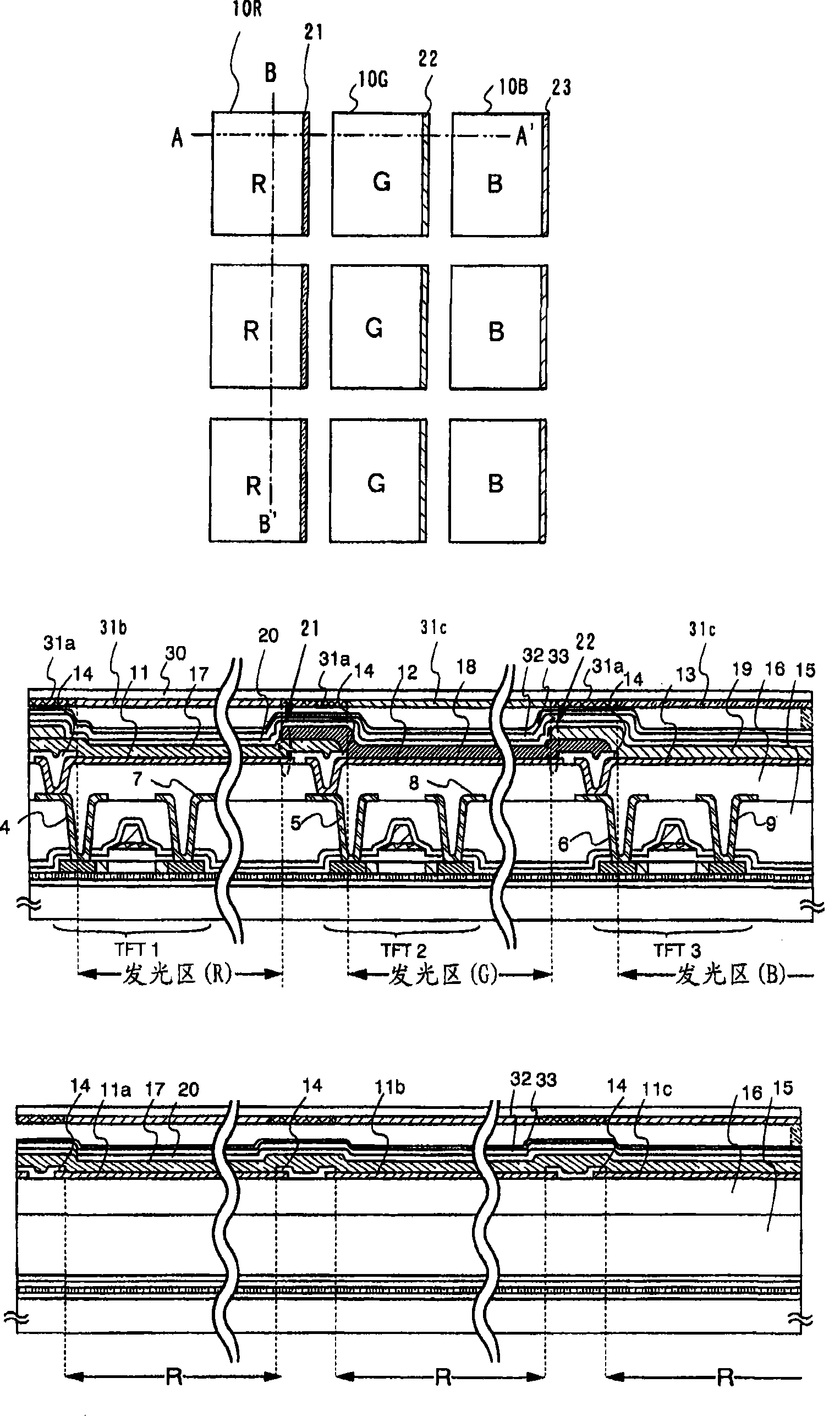
图1A是俯视图。图1A中,发光区10R是红色发光区,发光区10G是绿色发光区,发光区10B是蓝色发光区。全色发光装置通过这三种颜色的发光区来实现。Fig. 1A is a plan view. In FIG. 1A , the
另外,图1B是图1A沿着虚线段A-A’剖开的截面图。本发明中,红色发光EL层17的部分(例如,其中红色发光颜料Nile红加入到Alq3中的EL层)与绿色发光元件18的部分(例如,其中DMQd(二甲基喹吖(二)酮,dimethyl quinacridone)加入到Alq3中的EL层)重叠,形成叠层部分21,如图1B所示。另外,绿色发光EL层18的部分与蓝色发光EL层19(例如,其中二萘嵌苯(perylene)加入到BAlq中的EL层)的部分相重叠,形成叠层部分22。注意,虽然图1A-1C中示出了其中只有发光区的一侧(右侧边缘部分)重叠的实例,但是倘若四周部分的一部分重叠,对于哪一部分要重叠并没有限制。两个边缘,上侧边缘或下侧边缘都可以重叠。In addition, FIG. 1B is a cross-sectional view of FIG. 1A taken along the dotted line segment AA'. In the present invention, the part of the red light-emitting EL layer 17 (for example, the EL layer in which the red luminescent pigment Nile red is added to Alq 3 ) and the part of the green light-emitting element 18 (for example, in which DMQd (dimethylquinacridine (di) Ketone, dimethyl quinacridone) added to the EL layer in Alq 3 ) overlap to form a
EL层部分可以互相重叠的结构被使用,因此可以由使用红、绿和蓝色发光的全色平板显示器实现高清晰度和高孔径比,而不依赖于形成有机化合物层所采用的方法(诸如喷墨印刷,或旋涂)或者膜形成的精度。A structure in which the EL layers partially overlap each other can be used, so that high definition and high aperture ratio can be realized by a full-color flat panel display using red, green, and blue light emission, regardless of the method used to form the organic compound layer (such as inkjet printing, or spin coating) or film forming precision.
另外,图1B中TFT1是控制红色发光EL层17中流过的电流量的元件(p沟道TFT或n沟道TFT),参考编号4指源电极和漏电极中的一个,参考编号7指它们中的另一个。另外,TFT 12是控制绿色发光EL层18中流过的电流量的元件,参考编号5指源电极和漏电极中的一个,参考编号8指它们中的另一个。TFT 3是控制蓝色发光EL层19中流过的电流量的元件,参考编号6指源电极和漏电极中的一个,参考编号9指它们中的另一个。参考编号15和16指由有机绝缘材料或无机绝缘材料制成的夹层绝缘膜。In addition, TFT1 in FIG. 1B is an element (p-channel TFT or n-channel TFT) that controls the amount of current flowing in the red light-emitting
另外,参考编号11-13指有机发光元件阴极(或阳极),参考编号20指有机发光元件阳极(或阴极)。优选的是如果电极11-13是阳极,则使用p沟道TFT,优选的是如果电极11-13是阴极,则使用n沟道TFT。如果电极11-13是阴极,可以用具有较小功函数的材料(Al、Ag、Li、Ca、或它们的合金MgAg、MgIn、AlLi、CaF2、或CaN)。另外,如果电极11-13是阳极,可以使用选自包含Ti、TiN、TiSixNy、Ni、W、WSix、WNx、WSixNy、NbN、Mo、Cr、Pt、Zn、Sn、和In的组中的材料,以上述材料之一作为其主要成分的合金材料,具有以这些材料作为其主要成分的化合物的膜,或者这类膜的叠层膜。电极11-13的两边缘部分和边缘部分之间的部分用无机绝缘体14覆盖。这里,电极11-13用Cr形成作为阴极。电极20用具有高功函数的透明导电膜(ITO(氧化铟锡合金)、氧化铟和氧化锌的合金(In2O3-ZnO)、氧化锌(ZnO)等)形成作为阳极。发自每个发光元件的光穿过阳极20。另外,如果电极11-13是阳极,电极20是阴极,还可以用光透过的金属膜(诸如MgAg、MgIn、或AlLi)和透明导电膜的叠层膜。In addition, reference numbers 11-13 refer to cathodes (or anodes) of organic light emitting elements, and
然后用密封材料(图中没有示出)粘结密封衬底以便保留大约10-的间隙,这样就密封了所有发光元件。此外,滤色器形成于密封衬底30上,对应于每个象素,以提高色纯度。红色发光区10R对面形成红色化层31b,绿色发光区10G对面形成绿色化层31c,蓝色发光区10B对面形成蓝色化层31d。另外,发光区之外的区域用滤色器的黑色部分遮挡,即遮挡部分31a。注意,遮挡部分31a由金属膜(铬等)或包含黑色染料的有机材料构成。The sealing substrate is then bonded with a sealing material (not shown in the figure) so as to leave a gap of about 10-, thus sealing all the light-emitting elements. In addition, a color filter is formed on the sealing
因为形成滤色器,所以本发明中圆偏振片是不必要的。A circular polarizing plate is unnecessary in the present invention because a color filter is formed.
图1C是图1A沿着虚线段B-B’切割的情形中的横截面示图。以参考编号11a-11c表示的边缘部分和边缘部分之间的部分也用图1C中的无机绝缘体14覆盖。这里示出一个实例,其中红色发光EL层17是共同的,但是本发明不限于此,EL层还可以为发射同样颜色光的每个象素来形成。Fig. 1C is a cross-sectional view of Fig. 1A taken along the dashed line segment B-B'. The edge portions denoted by
进行了比较加在发光区10R、10G和10B上的电压和这些发光区发射光的亮度之间关系、以及加在叠层部分21-23上的电压和这些部分发射光的亮度之间关系的实验。实验结果示于图2D中。The relationship between the voltages applied to the light-emitting
图2D是示出横轴上电压(V)和纵轴上亮度(cd/m2)之间关系的图。图2D中圆圈记号所示的数据表示由三层,阴极、有机发光层、和阳极构造的发光元件的亮度和电压之间的关系。另外,三角记号所示的数据表示由四层,阳极、第一有机发光层、第二有机发光层、和阴极构造的发光元件的亮度和电压之间的关系。有机发光层由发光层、空穴输运层(HTL)和空穴注入层(HIL)的叠层构成。换言之,图2D中三角记号所示的数据是具有图2A所示叠层结构的发光元件的亮度和电压之间关系的图。这就是,阳极、第一有机发光层(第一发光层、第一空穴输运层、和第一空穴注入层)、第二有机发光层(第二发光层、第二空穴输运层、和第二空穴注入层)、以及阴极的叠层。FIG. 2D is a graph showing the relationship between voltage (V) on the horizontal axis and luminance (cd/m 2 ) on the vertical axis. The data indicated by circle marks in FIG. 2D represent the relationship between the luminance and the voltage of the light-emitting element constructed of three layers, the cathode, the organic light-emitting layer, and the anode. In addition, the data indicated by the triangle marks represent the relationship between the luminance and voltage of a light-emitting element constructed of four layers, an anode, a first organic light-emitting layer, a second organic light-emitting layer, and a cathode. The organic light-emitting layer is composed of a stack of a light-emitting layer, a hole transport layer (HTL) and a hole injection layer (HIL). In other words, the data shown by the triangle marks in FIG. 2D is a graph of the relationship between the luminance and the voltage of the light emitting element having the laminated structure shown in FIG. 2A. That is, the anode, the first organic light emitting layer (the first light emitting layer, the first hole transport layer, and the first hole injection layer), the second organic light emitting layer (the second light emitting layer, the second hole transport layer layer, and a second hole injection layer), and a stack of cathodes.
如图2D所示,发自具有阳极、两层有机发光层、和阴极的四层结构的发光元件的光的亮度与发自具有阳极、有机发光层、和阴极的三层结构的发光元件的光的亮度相比降低了大约4个数量级。可以预期这是因为当两个有机发光层互相叠加时形成的反向二极管,在其中电流流动变得更困难了。另外,膜厚度变得更厚,因而可以预期电阻变大,电流流动变得更困难。As shown in Figure 2D, the luminance of light emitted from a light-emitting element having a four-layer structure of an anode, two organic light-emitting layers, and a cathode is the same as that of a light-emitting element having a three-layer structure of an anode, an organic light-emitting layer, and a cathode. The brightness of the light is reduced by about 4 orders of magnitude. This is expected to be due to the reverse diode formed when two organic light-emitting layers are stacked on top of each other, in which current flow becomes more difficult. In addition, the film thickness becomes thicker, so it can be expected that the resistance becomes larger and the current flow becomes more difficult.
考虑一下这些结果怎样对应于图1A-1C,发自发光区10R、10G、和10B的光的亮度可以被认为是图2C所示叠层结构的亮度,发自叠层部分21-23的光的亮度可以被认为是图2A所示叠层结构的亮度。发自叠层部分21-23的光的亮度因而大约是发自发光区10R、10G和10B的光的亮度的千分之一。Considering how these results correspond to FIGS. 1A-1C , the brightness of light emitted from light-emitting
另外,在有机发光层中,至少一层是公用的,例如,空穴注入层,第一有机发光层的部分和第二有机发光层的部分可以在空穴注入层上彼此重叠。类似于图2A所示叠层结构的结果还可以从图2B所示的叠层结构中得到,其中空穴注入层是公用的,那就是具有阳极、第一有机发光层(第一发光层和第一空穴输运层)、第二有机发光层(第二发光层、第二空穴输运层、和第一空穴注入层)、和阴极的叠层结构的发光元件的亮度和电压的关系。In addition, among the organic light emitting layers, at least one layer is common, for example, a hole injection layer, and part of the first organic light emitting layer and part of the second organic light emitting layer may overlap each other on the hole injection layer. The result similar to the stacked structure shown in Figure 2A can also be obtained from the stacked structure shown in Figure 2B, wherein the hole injection layer is common, that is, there is an anode, a first organic light-emitting layer (the first light-emitting layer and The luminance and voltage of the light-emitting element with the stacked structure of the first hole transport layer), the second organic light-emitting layer (the second light-emitting layer, the second hole transport layer, and the first hole injection layer), and the cathode Relationship.
另外,具有部分不同于图1A-1C的结构的实例示于图3A-3C中。注意,为简单起见,图3A-3C中与图1A-1C中相同的部分用相同的参考编号。Additionally, examples having structures that differ in part from FIGS. 1A-1C are shown in FIGS. 3A-3C . Note that for simplicity, the same parts in FIGS. 3A-3C as in FIGS. 1A-1C are given the same reference numerals.
如图3A所示,这是一个实例,其中有机树脂制成的围堤25形成于发光区10R和发光区10G之间、以及发光区10G和发光区10B之间。虽然依赖于图形化精度,但是如果形成了围堤25,使发光区10G和发光区10B之间的距离更窄就不可避免地变得困难了。许多情形中,围堤形成于每个象素周围,但是图3A-3C采用了一种结构,其中围堤形成于每个象素列。As shown in FIG. 3A , this is an example in which a
图1A-1C中没有形成围堤,因而每个发光区之间的间隙可以做得很窄,可以实现高清晰度发光装置。No bank is formed in FIGS. 1A-1C , so the gap between each light-emitting area can be made very narrow, and a high-definition light-emitting device can be realized.
另外,形成保护膜33以提高图1A-1C和图3A-3C中的可靠性。保护膜33是以氮化硅或氮氧化硅作为其主要成分的绝缘膜。缓冲层32在形成保护膜之前形成以释放保护膜33之中的应力。缓冲层32可以通过使用DC溅射设备、RF溅射设备、或使用远距等离子体方法的设备由以氧化硅或氮氧化硅作为其主要成分的绝缘膜形成。另外,发出的光穿过图1A-1C和图3A-3C中的保护膜,因而优选的是保护膜的厚度尽可能的薄。In addition, a
如果透明导电膜(典型地I TO)用作图1A-1C和图3A-3C中的阳极或阴极,并且形成保护膜33使其接触透明导电膜,就有包含在透明导电膜中的杂质(In、Sn、Zn等)会混入保护膜33中的危险。在透明导电膜和保护膜之间形成缓冲层32还可以防止杂质混入保护膜。If a transparent conductive film (typically ITO) is used as an anode or a negative electrode in FIGS. 1A-1C and FIGS. 3A-3C, and a
另外,虽然图1A-1C和3A-3C中示出一种结构,其中光在向着密封衬底的方向从EL层中发射,穿过保护膜,当然本发明不限于这种结构。例如,光还可以在穿过夹层绝缘膜这样的方向上从EL层中发射。该情形中,滤色器可以适当地形成于上面形成了TFT的衬底上。In addition, although a structure is shown in FIGS. 1A-1C and 3A-3C in which light is emitted from the EL layer through the protective film in the direction toward the sealing substrate, the present invention is of course not limited to this structure. For example, light can also be emitted from the EL layer in such a direction as to pass through the interlayer insulating film. In this case, a color filter may be suitably formed on a substrate on which TFTs are formed.
实施方案样式2
这里用图5A和5B说明缓冲层和保护膜。Here, the buffer layer and the protective film are explained using FIGS. 5A and 5B.
图5A是示出光在图中箭头方向发射的情形中叠层结构实例的示意图。图5A中,参考编号200指阴极(阳极),参考编号201指EL层,参考编号202指阳极(阴极),参考编号203指应力释放层(缓冲层),参考编号204指保护膜。当光在图5A箭头方向发射时,具有透光性质的材料、非常薄的金属膜、或其叠层因而被用作电极202。FIG. 5A is a schematic view showing an example of a laminated structure in the case where light is emitted in the direction of the arrow in the figure. In FIG. 5A,
保护膜204使用由溅射得到的并以氮化硅或氮氧化硅作为其主要成分的绝缘膜。倘若用硅靶在含氮和氩的气氛中形成,就可以得到氮化硅膜。另外,还可以用氮化硅靶。形成保护膜之前形成缓冲层203以释放保护膜204中的内部膜应力。缓冲层203可以由以氧化硅和氮氧化硅为其主要成分的绝缘膜并用DC溅射设备、RF溅射设备或使用远距等离子体方法的设备来形成。当使用溅射设备时,缓冲层可以用硅靶在含氧和氩的气氛中,或在含氮、氧和氩的气氛中形成。另外,光穿过保护膜,因而优选的是保护膜的厚度尽可能的薄。The
发光元件可以用这类结构保护,因而可以得到高的可靠性。A light-emitting element can be protected with such a structure, and thus high reliability can be obtained.
图5B是示出光在图中箭头方向发射的情形中叠层结构实例的示意图。图4,参考编号300指阴极(或阳极),参考编号301指EL层,参考编号302指阳极(或阴极),参考编号303指应力释放层(缓冲层),参考编号304指保护膜。FIG. 5B is a schematic diagram showing an example of a laminated structure in the case where light is emitted in the direction of the arrow in the figure. 4,
发光元件可以用这种结构保护,类似于图5A的结构,因而能得到高的可靠性。A light-emitting element can be protected with this structure, similar to the structure of Fig. 5A, so that high reliability can be obtained.
另外,能够单独的制造图5A的叠层结构和图5B的叠层结构的制造设备(多室法)的实例示于图4。In addition, an example of a manufacturing apparatus (multi-chamber method) capable of independently manufacturing the laminated structure of FIG. 5A and the laminated structure of FIG. 5B is shown in FIG. 4 .
图4中,参考编号100a-100k和100m-100u指门(gate),参考编号101和119指转移室,参考编号102、104a、107、108、111、和114指输送器室,参考编号105、106R、106B、106G、109、110、112和113指膜形成室,参考编号103指预处理室,参考编号117a和117b指密封衬底装载室,参考编号115指配料室,参考编号116指密封室,参考编号118指紫外光照射室。In Fig. 4,
将上面事先已经形成了TFT和阴极的衬底输送到制造设备中并形成图5A所示叠层结构的过程示于图4中。The process of transporting the substrate on which the TFTs and cathodes have been formed in advance to the manufacturing equipment and forming the stacked structure shown in FIG. 5A is shown in FIG. 4 .
上面形成了TFT和阴极200的衬底首先置于转移室101。衬底然后输送到输送器室102,其与转移室101耦合。抽真空后优选的是惰性气体引入输送器室到大气压从而尽可能少的湿气和氧气存在于输送器室中。The substrate on which the TFT and
另外,用于抽取输送器室内真空的抽真空处理室与输送器室102连接。在抽真空处理室中提供磁悬浮涡轮分子泵、低温泵或干法泵(dry pump)。这样就可能将输送器室中达到的真空度设为10-5-10-6Pa,另外,可以控制杂质从泵一侧和抽气系统中的背扩散。诸如氮气或稀有气体的惰性气体用作引入气体以防止杂质引入到设备中。引入到设备中的气体在被引入到设备中以前用气体纯化设备提纯到很高的纯度。因而有必要提供气体纯化设备以便气体提纯以后再引入到膜形成设备中。这样,气体所含的氧、水和其它杂质可以事先被除去,随后可以防止这些杂质引入到设备中。In addition, an evacuation process chamber for extracting vacuum in the conveyor chamber is connected to the
另外,优选的是进行用于脱气的退火以除去衬底中所含的湿气和其它气体。衬底输送到与输送器室102连接的预处理室103中,可以在此进行退火。另外,如果有必要清洁阴极表面,衬底可以输送到与输送器室102连接的预处理室103中,可以在此进行清洁。In addition, it is preferable to perform annealing for degassing to remove moisture and other gases contained in the substrate. The substrate is transported into a
衬底104c接下来从输送器室102中输送到输送器室104中而不暴露于大气中,然后用输送器机构104b输送到膜形成室106R。然后红色发光EL层适当地形成于阴极200上。这里示出红色发光EL层通过蒸发形成的实例。上面要形成膜的衬底表面朝下放置于膜形成室106R中。注意,优选的是膜形成室在输送衬底到此之前被抽成真空。The
例如,真空抽到等于或小于5x10⁻³乇(Torr)(0.665Pa),优选的介于10-4-10-6Pa的真空度之后在膜形成室106R中进行蒸发。蒸发过程中有机化合物事先通过电阻加热气化,在蒸发过程中挡板(图中没有示出)打开时向着衬底散射。气化的有机化合物向上散射,穿过金属掩模(图中面有示出)中形成的开口部分,淀积到衬底上。注意,衬底的温度(T1)在蒸发过程中通过加热装置设为50-200℃,优选的在65-150℃之间。For example, evaporation is performed in the
对于其中形成三类EL层以提供全色的情形中,可以在膜形成室106R中完成膜形成以后在膜形成室106G和106B中连续地按顺序进行膜形成。In the case where three types of EL layers are formed to provide full colors, film formation may be sequentially performed successively in
接下来,在预定的EL层201形成于阴极200上以后,衬底从输送器室104输送到输送器室107而不暴露于大气中。另外,衬底然后从输送器室107中输送到输送器室108中而不暴露于大气中。Next, after a
接下来,衬底用放置于输送器室108中的输送器机构输送到膜形成室109中,由透明导电膜制成的阳极202适当地形成于EL层201上。这里多个靶置于膜形成室109中,使用至少具有由透明导电材料制成的靶和硅制成的靶的溅射设备。阳极202和应力释放层203因而可以在同一室中形成。注意,用来形成应力释放层203的专用膜形成室也可以单独地提供。该情形中也可以采用溅射设备(RF溅射或DC溅射)或者采用使用了远距等离子体方法的设备。Next, the substrate is conveyed into the
接下来,衬底从输送器室108输送到膜形成室113而不暴露于大气中,保护膜204形成于应力释放层203上。这里,配备了硅制成的靶或者氮化硅制成的靶的溅射设备提供在膜形成室113之中。氮化硅膜可以通过使膜形成室中的气氛变成氮气氛或含氮和氩的气氛来形成。Next, the substrate is conveyed from the
这样,被保护膜和应力释放层覆盖的发光元件通过上述工艺形成于衬底上。In this way, the light emitting element covered with the protective film and the stress release layer is formed on the substrate through the above process.
接下来,衬底从输送器室108输送到输送器室111中而不暴露于大气中,又从输送器室111输送到输送器室114中。Next, the substrate is transported from the
接下来,上面形成了发光元件的衬底从输送器室114输送到密封室116。注意,优选的是在密封室116中提供上面形成了密封材料的密封衬底。Next, the substrate on which the light emitting element is formed is transported from the
密封衬底从外面放入密封衬底装载室117a和117b中。注意,优选的是事先在真空中进行退火以除去诸如湿气的杂质。例如,退火可以在密封衬底装载室117a和117b中进行。对于密封材料形成于密封衬底上的情形,在输送器室108达到大气压之后,密封衬底从密封衬底装载室输送到配料室115中。然后形成密封材料用来粘结到上面形成发光元件的衬底上,具有所形成的密封材料的密封衬底输送到密封室116中。Sealed substrates are put into the sealed
然后具有所形成的密封材料的密封衬底和上面形成发光元件的衬底在真空中或在惰性气体气氛中互相粘结在一起。注意,虽然这里示出了密封材料形成于密封衬底上的实例,本发明不特别地局限于这个实例,密封材料还可以形成于具有已形成的发光元件的衬底上。Then the sealing substrate with the formed sealing material and the substrate on which the light emitting element is formed are bonded to each other in vacuum or in an inert gas atmosphere. Note that although an example in which the sealing material is formed on the sealing substrate is shown here, the present invention is not particularly limited to this example, and the sealing material may also be formed on the substrate having the formed light emitting element.
接下来,粘结的一对衬底从输送器室114输送到紫外光照射室118中。UV光在紫外光照射室118中照射,这样硬化密封材料。注意,虽然紫外凝固树脂在这里用作密封材料,但倘若是粘性材料,在密封材料上没有设置特别的限制。Next, the bonded pair of substrates is conveyed from the
然后衬底对从输送器室114输送到转移室119中,并取出来。The substrate pair is then transported from the
这样就通过使用图4所示的制造设备完成了直到将发光元件完全密封到密闭空间中的工艺过程,而不暴露于大气中,因而制造具有高可靠性的发光装置变成可能。This completes the process up to the complete sealing of the light-emitting element into the closed space without exposure to the atmosphere by using the manufacturing equipment shown in FIG. 4, thus making it possible to manufacture a light-emitting device with high reliability.
注意,还可以使用串联(inline)膜形成设备。Note that an inline film forming apparatus may also be used.
下面示出形成图5B所示叠层结构的过程。上面事先形成了TFT和阳极的衬底输送到图4所示的制造设备中。The process of forming the laminated structure shown in Fig. 5B is shown below. The substrate on which the TFTs and anodes were previously formed was transported to the manufacturing apparatus shown in FIG. 4 .
首先,上面形成了TFT和阳极300的衬底放置在转移室101中。然后衬底输送到与转移室101连接的输送器室102中。优选的是进行真空蒸发之后在大气压下向输送器室中引入惰性气体使得尽可能少的湿气和氧气存在于输送器室内。透明导电材料用作形成阳极300的材料,可以用铟锡化合物、氧化锌等。然后衬底输送到与输送器室102连接的预处理室103中。清洁、氧化工艺、热处理工艺等可以在预处理室中的阳极表面上进行。作为清洁阳极表面的方法,进行真空紫外光照射或氧等离子体处理。另外,作为氧化工艺,也可以在加热到100-120℃的温度下在含氧的气氛中进行紫外光的照射,这对于阳极是诸如I TO的氧化物的情形中是有效的。另外,作为热处理工艺,热处理可以在衬底能够承受的大于或等于50℃,优选的是65℃和150℃之间这样的热处理温度下在真空中进行。这样吸附在衬底上诸如氧和湿气这样的杂质和形成于衬底上的膜内诸如氧和湿气这样的杂质可以被除去。特别是,EL材料容易由于诸如氧和水这样的杂质退化,因而在蒸发前进行真空中热处理是有效的。First, the substrate on which the TFT and
然后衬底104c从输送器室102中输送到输送器室104中而不暴露于大气中,然后用输送器机构104b输送到膜形成室105中。然后EL层的一层,诸如空穴注入层或空穴输运层,适当地形成于阳极300上。这里示出通过蒸发形成EL层的实例。上面要形成膜的衬底表面朝下放在膜形成室105中。注意,优选的是在衬底输送进来之前在膜形成室中进行抽真空。The
然后衬底用输送器机构104b输送到膜形成室106R中而不暴露于大气中,红色发光EL层适当地形成于空穴注入层或空穴输运层上。The substrate is then conveyed by the conveyor mechanism 104b into the
对于其中形成三类EL层以提供全色的情形,可以在膜形成室106R中完成了膜形成之后在膜形成室106G和106B中按顺序进行膜形成。For the case where three types of EL layers are formed to provide full colors, film formation may be sequentially performed in the
然后在预定的EL层301形成于阳极300上之后,衬底从输送器室104中输送到输送器室107中而不暴露于大气中。此外,衬底然后从输送器室107中输送到输送器室108中而不暴露于大气中。Then after a
然后衬底用配备在输送器室108中的输送器机构输送到膜形成室110或112中,由金属材料制成的阴极302适当地形成于EL层301上。这里膜形成室111是蒸发设备或溅射设备。The substrate is then transported into the
然后衬底从输送器室108输送到膜形成设备113中而不暴露于大气中,形成应力释放层303和保护膜304。这里,膜形成室113中提供了配备有硅制成的靶、氮化硅制成的靶、或氧化硅制成的靶的溅射设备。氧化硅膜、氮氧化硅膜、或氮化硅膜可以通过使膜形成室中的气氛变成氮气气氛、含氮和氩的气氛、或含氧、氮和氩的气氛来形成。The substrate is then conveyed from the
这样通过上述工艺,被保护膜和应力释放层覆盖的发光层就形成于衬底上。Thus, through the above process, the light emitting layer covered by the protective film and the stress release layer is formed on the substrate.
接下来的工艺步骤与形成图5A所示叠层结构的过程相同,因而其说明在这里就省略了。Subsequent process steps are the same as those for forming the stacked structure shown in FIG. 5A, and thus descriptions thereof are omitted here.
这样图5A所示的叠层结构和图5B所示的叠层结构通过图4所示的制造设备都可以形成了。In this way, both the laminated structure shown in FIG. 5A and the laminated structure shown in FIG. 5B can be formed by the manufacturing equipment shown in FIG. 4 .
另外,实施方案样式2可以与实施方案样式1自由地组合。In addition,
具有上述结构的本发明通过下面所示实施方案更详细地说明。The present invention having the above structure is explained in more detail by the embodiments shown below.
实施方案1
本实施方案中,将说明在绝缘膜上制造的有源矩阵型发光装置。图6是有源矩阵型发光装置的截面图。作为有源元件,这里使用薄膜晶体管(下文中称作TFT),也可以使用MOS晶体管。In this embodiment, an active matrix type light emitting device fabricated on an insulating film will be described. Fig. 6 is a cross-sectional view of an active matrix type light emitting device. As active elements, thin film transistors (hereinafter referred to as TFTs) are used here, and MOS transistors may also be used.
顶部栅TFT(特别是平面TFT)作为实例示出,也可以使用底部栅TFT(典型地是反向交错的TFT,inversely staggered TFT)。A top-gate TFT (particularly a planar TFT) is shown as an example, and a bottom-gate TFT (typically an inversely staggered TFT) may also be used.
本实施方案中使用由硼硅酸钡玻璃或硼硅酸铝玻璃制成的衬底800,可以使用表面上形成了绝缘膜的不锈钢衬底、金属衬底、硅衬底、石英衬底。还可以使用具有能承受本实施方法中热处理温度的热阻性的塑料衬底,另外可以使用柔性衬底。The
其次,通过等离子体CVD在400℃的温度下用SiH4、NH3、和N2O作为原料气体在耐热玻璃衬底(衬底800)上形成0.7mm厚度的氮氧化硅膜作为基绝缘膜的下层801(氮氧化硅膜的组分比:Si=32%,O=27%,N=24%,H=17%)。氮氧化硅膜具有50nm(优选的10-200nm)的厚度。膜表面用臭氧水清洗,然后表面上的氧化物膜用稀氟酸(稀释至1/100)除去。其次,通过等离子体CVD在400℃的温度下用SiH4和N2O作为原料气体形成氮氧化硅膜作为基绝缘膜的上层802(氮氧化硅膜的组分比:S i=32%,O=59%,N=7%,H=2%)。氮氧化硅膜具有100nm(优选的50-200nm)的厚度,放在下层上面以形成叠层。不要将叠层暴露于空气中,通过等离子体CVD在300℃的温度下用SiH4作为原料气体在叠层上形成具有非晶结构的半导体膜(这里是非晶硅膜)。半导体膜(这里使用非晶硅膜)在厚度上是54nm(优选的是25-200nm)。Next, a silicon oxynitride film with a thickness of 0.7 mm was formed as a base insulating film on a heat-resistant glass substrate (substrate 800) by plasma CVD at a temperature of 400° C. using SiH 4 , NH 3 , and N 2 O as raw material gases. The
本实施方案中基绝缘膜具有两层结构。然而,基绝缘膜可以是主要含硅的两层以上绝缘膜或是单层绝缘膜。半导体膜的材料不受限制,但是优选的是用硅或锗硅合金(SixGe1-x(X=0.0001-0.02))通过已知的方法(溅射、LPCVD、等离子体CVD等)形成半导体膜。所用的等离子体CVD设备可以是一个晶片一个晶片处理的设备,或者是整批处理的设备。基绝缘膜和半导体膜可以在同一个室中连续形成以避免与空气接触。The base insulating film in this embodiment has a two-layer structure. However, the base insulating film may be a two-layer or more insulating film mainly containing silicon or a single-layer insulating film. The material of the semiconductor film is not limited, but it is preferably formed by known methods (sputtering, LPCVD, plasma CVD, etc.) semiconductor film. The plasma CVD equipment used may be a wafer-by-wafer processing equipment, or a batch processing equipment. The base insulating film and the semiconductor film can be successively formed in the same chamber to avoid contact with air.
清洗具有非晶结构的半导体膜表面,然后大约2nm厚度的非常薄的氧化物膜用臭氧水形成于表面上。其次,半导体膜用微量杂质元素(硼或磷)掺杂以控制TFT的阈值。这里,非晶硅膜通过离子掺杂用硼掺杂,其中硼烷(B2H6)用等离子体激发而不发生质量分离。掺杂条件包括将加速电压设定到15kV,用氢稀释硼烷到1%所得到气体的流速设定到30sccm,剂量设定到2x10¹²原子/cm2。The surface of the semiconductor film having an amorphous structure is cleaned, and then a very thin oxide film with a thickness of about 2 nm is formed on the surface with ozone water. Second, the semiconductor film is doped with a trace amount of impurity elements (boron or phosphorus) to control the threshold of the TFT. Here, the amorphous silicon film is doped with boron by ion doping in which borane (B 2 H 6 ) is excited with plasma without mass separation. The doping conditions included setting the acceleration voltage to 15 kV, the flow rate of the gas obtained by diluting borane with hydrogen to 1% to 30 sccm, and the dose to 2×10 12 atoms/cm 2 .
其次,含10ppm重量的镍的醋酸镍溶液用旋转器涂覆。镍元素可以通过溅射喷射到整个表面上来代替涂覆。Next, a nickel acetate solution containing 10 ppm by weight of nickel was coated with a spinner. Nickel can be sprayed onto the entire surface by sputtering instead of coating.
半导体膜受到热处理以使它晶化,得到具有晶体结构的半导体膜。热处理在电炉中实现或通过强光照射实现。当采用在电炉中热处理时,温度设为500-650℃,处理持续4-24小时。这里,在用于脱氢的热处理(500℃,1小时)之后通过用于晶化的热处理(在550℃,4小时)得到具有晶体结构的硅膜。虽然这里通过使用电炉的热处理来晶化半导体膜,但是还可以通过能够在短时间内实现氢化的灯退火设备来晶化。The semiconductor film is subjected to heat treatment to crystallize it, resulting in a semiconductor film having a crystal structure. Heat treatment is achieved in an electric furnace or by exposure to intense light. When heat treatment in an electric furnace is adopted, the temperature is set at 500-650° C., and the treatment lasts for 4-24 hours. Here, a silicon film having a crystal structure is obtained by heat treatment for crystallization (at 550° C., 4 hours) after heat treatment for dehydrogenation (500° C., 1 hour). Although the semiconductor film is crystallized here by heat treatment using an electric furnace, it may also be crystallized by lamp annealing equipment capable of achieving hydrogenation in a short time.
在具有晶体结构的硅膜表面上的氧化物膜用稀释的氟酸等除去之后,晶化非晶半导体膜时,采用连续振荡固体激光和基波的二到四次谐波以得到大晶粒尺寸。由于激光照射在空气或在氧气气氛中进行,结果是在表面上形成氧化物膜。典型地,采用Nd:YVO4激光(基波:1064nm)的二次谐波(532nm)或三次谐波(355nm)。当使用连续波激光器时,发射10W功率连续波YVO4激光器的激光用非线性光学元件转变成谐波。另外,谐波还可以通过将YVO4晶体和非线性元件放在谐振室中得到。谐波优选的用光学系统在照射面上成形为长形或椭圆形激光,然后照射目标。这点所需要的能量密度大约是0.01-100MW/cm2(优选的是0.1-10MW/cm2)。照射的时候,半导体膜以10-2000cm/s的速度相对于激光移动。When crystallizing an amorphous semiconductor film after the oxide film on the surface of a silicon film having a crystal structure is removed with diluted hydrofluoric acid, etc., a continuous-wave solid-state laser and the second to fourth harmonics of the fundamental wave are used to obtain large crystal grains size. Since laser irradiation is performed in air or in an oxygen atmosphere, an oxide film is formed on the surface as a result. Typically, the second harmonic (532 nm) or third harmonic (355 nm) of Nd:YVO 4 laser (fundamental wave: 1064 nm) is used. When using a continuous wave laser, the laser emitting 10W power continuous wave YVO 4 laser is converted into harmonics with nonlinear optical elements. In addition, harmonics can also be obtained by placing YVO 4 crystals and nonlinear components in the resonant chamber. Harmonics are preferably shaped into elongated or elliptical lasers on the irradiated surface with an optical system, and then illuminate the target. The energy density required for this is about 0.01-100 MW/cm 2 (preferably 0.1-10 MW/cm 2 ). During irradiation, the semiconductor film moves relative to the laser light at a speed of 10-2000 cm/s.
当然,尽管在连续振荡YVO4激光的二次谐波照射在其上面之前,TFT可以用具有晶体结构的硅膜形成,因为上面照射了激光的硅膜具有改善了的结晶性并且TFT的电性能提高了,所以优选的是使用激光照射在上面之后具有结晶结构的硅膜以形成TFT。例如,尽管,当使用激光照射在其上面之前就具有结晶结构的硅膜形成TFT时,迁移率几乎是300cm2/Vs,当TFT通过使用激光照射在其上面之后具有结晶结构的硅膜形成时,迁移率极端地提高到大约500-600cm2/Vs。Of course, although the TFT can be formed with a silicon film having a crystalline structure before the second harmonic of the continuous oscillation YVO 4 laser is irradiated thereon, because the silicon film on which the laser is irradiated has improved crystallinity and the electrical properties of the TFT improved, so it is preferable to use a silicon film having a crystalline structure after laser irradiation thereon to form a TFT. For example, although, when a TFT is formed using a silicon film having a crystalline structure before laser irradiation thereon, the mobility is almost 300 cm 2 /Vs, when a TFT is formed by using a silicon film having a crystalline structure after laser irradiation thereon , the mobility is extremely increased to about 500-600 cm 2 /Vs.
在用镍作为提高硅结晶性的金属元素进行晶化之后,连续振荡YVO4激光照射在其上面,虽然不限于此,在形成具有非晶结构的硅膜并进行用于脱氢的热处理之后,具有结晶结构的硅膜可以通过照射连续振荡YVO4激光的二次谐波得到。After crystallization with nickel as a metal element that improves the crystallinity of silicon, continuous oscillation YVO 4 laser is irradiated thereon, although not limited thereto, after forming a silicon film with an amorphous structure and performing heat treatment for dehydrogenation, A silicon film with a crystalline structure can be obtained by irradiating the second harmonic of a continuous oscillation YVO 4 laser.
脉冲振荡激光可以用作连续振荡激光的替代物。在使用脉冲振荡的准分子激光的情形中,优选的是频率设为300Hz,激光能量密度设为100-1000mJ/cm2(典型地是200-800mJ/cm2)。这里,激光可以重叠(overlap)50-98%。A pulsed oscillation laser can be used as a substitute for a continuous oscillation laser. In the case of using a pulsed excimer laser, it is preferable that the frequency is set to 300 Hz and the laser energy density is set to 100-1000 mJ/cm 2 (typically 200-800 mJ/cm 2 ). Here, the lasers may overlap by 50-98%.
激光照射形成的氧化物膜用稀氟酸除去,然后表面用臭氧水处理120秒以形成由1-5nm总厚度的氧化物膜构成的阻挡层。这里阻挡层用臭氧水形成,但是还可以通过在氧气氛中紫外光照射氧化具有晶体结构的半导体膜表面形成,或者通过氧等离子体处理氧化具有晶体结构的半导体膜表面或使用等离子体CVD、溅射或蒸发形成大约1-10nm厚氧化物膜。通过激光照射形成的氧化物膜可以在阻挡层形成之前被除去。The oxide film formed by laser irradiation was removed with dilute hydrofluoric acid, and then the surface was treated with ozone water for 120 seconds to form a barrier layer consisting of an oxide film with a total thickness of 1-5 nm. Here the barrier layer is formed with ozone water, but it can also be formed by oxidizing the surface of a semiconductor film having a crystal structure by ultraviolet light irradiation in an oxygen atmosphere, or oxidizing the surface of a semiconductor film having a crystal structure by oxygen plasma treatment or using plasma CVD, sputtering, etc. Oxide films with a thickness of about 1-10 nm are formed by irradiation or evaporation. The oxide film formed by laser irradiation can be removed before the barrier layer is formed.
其次,通过等离子体CVD或溅射在阻挡层上形成包含氩的非晶硅膜以作为吸取位。非晶硅膜的厚度是50-400nm,这里是150nm。通过使用硅靶的溅射以达到0.3Pa的形成压力在氩气氛中形成非晶硅膜。Next, an amorphous silicon film containing argon is formed as a gettering site on the barrier layer by plasma CVD or sputtering. The thickness of the amorphous silicon film is 50-400nm, here 150nm. An amorphous silicon film was formed in an argon atmosphere by sputtering using a silicon target at a formation pressure of 0.3 Pa.
之后,热处理在650℃于电炉中进行3分钟,用于吸取以减少具有晶体结构的半导体膜中的镍含量。可以使用灯退火设备代替电炉。After that, heat treatment was performed at 650° C. for 3 minutes in an electric furnace for gettering to reduce the nickel content in the semiconductor film having a crystal structure. Lamp annealing equipment can be used instead of electric furnaces.
用阻挡层作为刻蚀阻挡物,吸取位,也就是含氩的非晶硅膜被选择性的除去。然后,阻挡层用稀氟酸被选择性的除去。在吸取过程中镍趋向于向具有高氧浓度的区域运动,因而在吸取之后除去为氧化物膜的阻挡层是理想的。Using the stopper layer as an etch stopper, the gettering sites, that is, the argon-containing amorphous silicon film, are selectively removed. Then, the barrier layer is selectively removed with dilute hydrofluoric acid. Nickel tends to move toward regions with high oxygen concentration during the sucking process, so it is desirable to remove the barrier layer as an oxide film after the sucking.
其次,利用臭氧水薄的氧化物膜在所得到的包含晶体结构的硅膜(还称作多晶硅膜)表面上形成。然后形成抗蚀剂掩模,刻蚀硅膜以形成彼此之间互相分离并具有所需形状的岛状半导体层。半导体膜形成之后,除去抗蚀剂掩模。Next, a thin oxide film is formed on the surface of the resulting silicon film (also referred to as a polysilicon film) containing a crystal structure using ozone water. A resist mask is then formed, and the silicon film is etched to form island-shaped semiconductor layers separated from each other and having a desired shape. After the semiconductor film is formed, the resist mask is removed.
氧化物膜用含氟酸的腐蚀剂除去,同时,清洗硅膜表面。然后,形成主要含硅的绝缘膜来作为栅绝缘膜803。这里栅绝缘膜是通过等离子体CVD形成的氮氧硅膜(组成比:Si=32%、O=59%、N=7%、H=2%),具有115nm的厚度。The oxide film is removed with an etchant containing fluoric acid, and at the same time, the surface of the silicon film is cleaned. Then, an insulating film mainly containing silicon is formed as the
其次,具有20-100nm厚度的第一导电膜和具有100-400nm厚度的第二导电膜的叠层形成于栅绝缘膜上。本实施方案中,具有50nm厚度的氮化钽膜形成于栅绝缘膜803上,然后具有370nm的钨膜放置在上面。导电膜通过下面所示的过程图形化以形成栅电极和线路。Next, a stack of a first conductive film having a thickness of 20-100 nm and a second conductive film having a thickness of 100-400 nm is formed on the gate insulating film. In this embodiment, a tantalum nitride film having a thickness of 50 nm is formed on the
第一导电膜和第二导电膜的导电材料是选自包含Ta、W、Ti、Mo、Al、和Cu的组中的元素,或合金或者主要包含上面这些元素的化合物。第一导电膜和第二导电膜可以是半导体膜,典型地是多晶硅膜,以磷或其它杂质元素掺杂,或可以是Ag-Pd-Cu合金膜。本发明不限于两层结构的导电膜。例如,可以采用包含50nm厚钨膜、500nm厚铝-硅合金(Al-Si)膜、和30nm厚氮化钛膜依次分层的三层结构。当采用三层结构时,第一导电膜的钨可以用氮化钨代替,第二导电膜的铝-硅合金(Al-Si)膜可以用铝-钛合金(Al-Ti)膜代替,第三导电膜的氮化钛膜可以用钛膜代替。另外,可以使用单层导电膜。The conductive material of the first conductive film and the second conductive film is an element selected from the group consisting of Ta, W, Ti, Mo, Al, and Cu, or an alloy or a compound mainly containing the above elements. The first conductive film and the second conductive film may be semiconductor films, typically polysilicon films, doped with phosphorus or other impurity elements, or may be Ag-Pd-Cu alloy films. The present invention is not limited to a conductive film of a two-layer structure. For example, a three-layer structure including a 50 nm thick tungsten film, a 500 nm thick aluminum-silicon alloy (Al—Si) film, and a 30 nm thick titanium nitride film layered in this order may be employed. When a three-layer structure is adopted, the tungsten of the first conductive film can be replaced by tungsten nitride, the aluminum-silicon alloy (Al-Si) film of the second conductive film can be replaced by an aluminum-titanium alloy (Al-Ti) film, and the second conductive film can be replaced by an aluminum-titanium alloy (Al-Ti) film. The titanium nitride film of the three conductive films may be replaced by a titanium film. Alternatively, a single-layer conductive film may be used.
ICP(诱导耦合等离子体)刻蚀优选的用于第一导电膜和第二导电膜的刻蚀(第一刻蚀处理和第二刻蚀处理)。通过使用ICP刻蚀和调整刻蚀条件(加到线圈状电极上的电功率量的多少,加到衬底侧电极上的电功率量的多少,衬底侧电极的温度等),膜可以被刻蚀并如所需要的那样形成锥形。第一刻蚀处理在抗蚀剂制成的掩模形成之后进行。第一刻蚀条件包括在1Pa压力下向线圈型电极上施加700W的RF(13.56MHz)功率,采用CF4、Cl2、和O2作为刻蚀气体,并设定气流速率比为25∶25∶10(s ccm)。衬底侧(样品台)还接受150W的RF(13.56MHz)功率以施加基本上负的自偏压。衬底侧电极的面积(尺寸)是12.5cmX12.5cm,线圈型电极是直径25cm的圆盘(这里是上面配备有线圈的石英盘)。W膜在这些第一刻蚀条件下刻蚀以在边缘周围成为锥形。之后,不除去抗蚀剂构成的掩模将第一刻蚀条件转变成第二刻蚀条件。第二刻蚀条件包括使用CF4和Cl2作为刻蚀气体,设定其气流速率比为30∶30(sccm),并在1Pa的压力下给予线圈型电极500W的RF(13.56MHz)功率以产生等离子体用来刻蚀大约30秒。衬底侧(样品台)还接受20W的RF功率(13.56MHz)以施加基本上负的自偏压。在其中使用CF4和Cl2的混合物的第二刻蚀条件下,W膜和TaN膜被刻蚀到几乎同样的程度。第一刻蚀条件和第二刻蚀条件组成第一刻蚀处理。ICP (Inductively Coupled Plasma) etching is preferably used for etching of the first conductive film and the second conductive film (first etching treatment and second etching treatment). By using ICP etching and adjusting the etching conditions (the amount of electric power applied to the coil-shaped electrode, the amount of electric power applied to the substrate-side electrode, the temperature of the substrate-side electrode, etc.), the film can be etched And taper as desired. The first etching treatment is performed after the mask made of resist is formed. The first etching conditions include applying 700W of RF (13.56MHz) power to the coil-type electrode under 1Pa pressure, using CF4 , Cl2 , and O2 as etching gases, and setting the gas flow rate ratio to 25:25 : 10 (sccm). The substrate side (sample stage) also received 150 W of RF (13.56 MHz) power to apply a substantially negative self-bias. The area (dimensions) of the substrate-side electrode was 12.5 cm×12.5 cm, and the coil-type electrode was a disc (here, a quartz disc provided with a coil thereon) with a diameter of 25 cm. The W film is etched under these first etching conditions to become tapered around the edges. Thereafter, the first etching condition is changed to the second etching condition without removing the mask made of the resist. The second etching condition included using CF4 and Cl2 as etching gas, setting the gas flow rate ratio to 30:30 (sccm), and giving the coil-type electrode 500W of RF (13.56MHz) power under the pressure of 1Pa to Plasma is generated for etching for about 30 seconds. The substrate side (sample stage) also received 20 W of RF power (13.56 MHz) to apply a substantially negative self-bias. Under the second etching condition in which a mixture of CF4 and Cl2 was used, the W film and the TaN film were etched to almost the same extent. The first etching condition and the second etching condition constitute a first etching process.
其次是在抗蚀剂掩模保留不动时接着第二刻蚀处理。第三刻蚀条件包括使用CF4和Cl2作为刻蚀气体,设定其气流速率比为30∶30(sccm),在1Pa的压力下给予线圈型电极500W的RF(13.56MHz)功率以产生等离子体用于刻蚀60秒。衬底侧(样品台)还接受20W的RF功率(13.56MHz)以施加基本上负的自偏压。然后,不除去抗蚀剂掩模将第三刻蚀条件转变为第四刻蚀条件。第四刻蚀条件包括使用CF4、Cl2、和O2作为刻蚀气体,设定其气流速率比为20∶20∶20(sccm),在1Pa的压力下给予线圈型电极500W的RF(13.56MHz)功率以产生等离子体用于刻蚀大约20秒。衬底侧(样品台)还接受20W的RF功率(13.56MHz)以施加基本上负的自偏压。第三刻蚀条件和第四刻蚀条件组成了第二刻蚀处理。在这个阶段,形成具有第一导电层804a作为下层和第二导电层804b作为上层的栅电极804和线路805-807。This is followed by a second etch process while the resist mask is left untouched. The third etching condition includes using CF 4 and Cl 2 as etching gas, setting the gas flow rate ratio to 30:30 (sccm), and giving 500W of RF (13.56MHz) power to the coil-shaped electrode under a pressure of 1Pa to generate Plasma was used to etch for 60 seconds. The substrate side (sample stage) also received 20 W of RF power (13.56 MHz) to apply a substantially negative self-bias. Then, the third etching condition is changed to the fourth etching condition without removing the resist mask. The fourth etching condition includes using CF 4 , Cl 2 , and O 2 as etching gases, setting the gas flow rate ratio to 20:20:20 (sccm), and giving the coil-type electrode 500 W of RF ( 13.56 MHz) power to generate plasma for etching for about 20 seconds. The substrate side (sample stage) also received 20 W of RF power (13.56 MHz) to apply a substantially negative self-bias. The third etching condition and the fourth etching condition constitute the second etching process. At this stage, the gate electrode 804 and the wirings 805-807 are formed having the first conductive layer 804a as the lower layer and the second
其次,为了第一掺杂处理除去抗蚀剂构成的掩模以便用栅电极804-807作为掩模来掺杂整个表面。第一掺杂处理采用离子掺杂或离子注入。这里,离子掺杂条件是剂量设定为1.5X10¹⁴原子/cm2,加速电压设定为60-100keV。作为给出n型导电性的杂质元素,典型地使用磷(P)或砷(As)。第一杂质区(n-区)822-825以自对准的方式形成。Next, the mask made of resist is removed for the first doping process to dope the entire surface using the gate electrodes 804-807 as a mask. The first doping treatment employs ion doping or ion implantation. Here, the ion doping conditions are that the dose is set at 1.5X10 14 atoms/cm 2 , and the accelerating voltage is set at 60-100keV. As an impurity element giving n-type conductivity, phosphorus (P) or arsenic (As) is typically used. The first impurity regions (n - regions) 822-825 are formed in a self-aligned manner.
重新形成由抗蚀剂构成的掩模。这时,由于开关TFT 903的关电流值降低了,所以形成掩模以便与半导体层的沟道形成区重叠,所述导体层形成象素部分901的开关TFT 903和其一部分。形成掩模以保护半导体层的沟道形成区,所述导体层形成驱动器电路的p沟道TFT906和其外围。另外,形成掩模以便与形成象素部分901的电流控制TFT 904和其外围的半导体层的沟道形成区重叠。A mask made of resist is reformed. At this time, since the off-current value of the switching
与栅电极的部分重叠的杂质区(n-区)通过用抗蚀剂构成的掩模选择性地进行第二掺杂处理来形成。第二掺杂处理采用离子掺杂或离子注入。这里使用离子掺杂,用氢稀释磷化氢(PH3)到5%得到的气体流速设为30sccm,剂量设为1.5X10¹⁴原子/cm2,加速电压设为90keV。该情形中由抗蚀剂构成的掩模和第二导电层作为阻止给出n型导电性的杂质元素的掩模,并形成杂质区311和312。第二杂质区用给出n型导电性的杂质元素在1X1016-1X1017原子/cm3的浓度范围内掺杂。这里,与第二杂质区相同浓度范围被称作n-区。An impurity region (n - region) partially overlapping the gate electrode is formed by selectively performing a second doping process using a mask made of resist. The second doping treatment employs ion doping or ion implantation. Ion doping is used here, the gas flow rate obtained by diluting phosphine (PH 3 ) to 5% with hydrogen is set to 30 sccm, the dose is set to 1.5X10 14 atoms/cm 2 , and the accelerating voltage is set to 90 keV. The mask made of resist and the second conductive layer in this case serve as a mask for blocking impurity elements giving n-type conductivity, and impurity regions 311 and 312 are formed. The second impurity region is doped with an impurity element giving n-type conductivity in a concentration range of 1X10 16 -1X10 17 atoms/cm 3 . Here, the same concentration range as the second impurity region is called an n - region.
不除去抗蚀剂构成的掩模进行第三掺杂处理。第三掺杂处理采用离子掺杂或离子注入。作为给出n型导电性的杂质元素,典型地使用磷(P)和砷(As)。这里,使用离子掺杂,用氢稀释磷化氢(PH3)到5%得到的气体流速设为40s ccm,剂量设为2X10¹⁵原子/cm2,加速电压设为80keV。该情形中,抗蚀剂构成的掩模、第一导电层和第二导电层作为阻止给出n型导电性的杂质元素的掩模,并形成第三杂质区813、814、826-828。第三杂质区用给出n型导电性的杂质元素在1X1020-1X1021原子/cm3的浓度范围内掺杂。这里,与第三杂质区同样浓度的范围被称作n+区。The third doping treatment is performed without removing the resist mask. The third doping treatment employs ion doping or ion implantation. As impurity elements giving n-type conductivity, phosphorus (P) and arsenic (As) are typically used. Here, using ion doping, the gas flow rate obtained by diluting phosphine (PH 3 ) to 5% with hydrogen was set at 40 s ccm, the dose was set at 2×10 15 atoms/cm 2 , and the accelerating voltage was set at 80 keV. In this case, the mask made of resist, the first conductive layer, and the second conductive layer serve as a mask for blocking impurity elements giving n-type conductivity, and third impurity regions 813, 814, 826-828 are formed. The third impurity region is doped with an impurity element giving n-type conductivity in a concentration range of 1×10 20 -1×10 21 atoms/cm 3 . Here, a range having the same concentration as the third impurity region is called an n + region.
除去抗蚀剂掩模并形成新的抗蚀剂掩模之后,进行第四掺杂处理。形成第四杂质区818、819、832、833和第五杂质区816、817、830、831,其中给出p型导电性的杂质元素通过第四掺杂处理添加到形成p沟道TFT的半导体层中。After the resist mask is removed and a new resist mask is formed, a fourth doping process is performed.
给出p型导电性的杂质元素的浓度设为1X10²⁰-1X10²¹原子/cm3以添加到第四杂质区818、819、832和833中。作为区(n-区)的第四杂质区818、819、832和833在前面的步骤中已经用磷(P)掺杂,但以浓度是磷浓度1.5-3倍的给出p型导电性的杂质元素掺杂以得到p型导电性。这里,具有与第四杂质区相同浓度范围的区也称作p+区。The concentration of the impurity element giving p-type conductivity is set to 1×10 20 -1×10 21 atoms/cm 3 to be added to the
第五杂质区816、817、830和831形成于与第二导电层锥形部分重叠的区域中。给出p型导电性的杂质元素在1X10¹⁸-1X10²⁰原子/cm3的浓度范围添加于此。这里,具有与第五杂质同样浓度范围的区被称作p-区。
通过上述步骤,具有n型或p型导电性的杂质区形成于各半导体层中。导电层804-807变成TFT的栅电极。Through the above steps, an impurity region having n-type or p-type conductivity is formed in each semiconductor layer. Conductive layers 804-807 become gate electrodes of TFTs.
形成绝缘以覆盖几乎整个表面(没有示出)。本实施方案中,具有50nm厚度的氧化硅膜用等离子体CVD法形成。当然,绝缘膜不限于氧化硅膜,可以用含硅的其它绝缘膜的叠层或单层。Insulation is formed to cover almost the entire surface (not shown). In this embodiment, a silicon oxide film having a thickness of 50 nm is formed by plasma CVD. Of course, the insulating film is not limited to a silicon oxide film, and a stack or a single layer of other insulating films containing silicon may be used.
下一个步骤是用于掺杂各个半导体层的杂质元素的激活处理。激活步骤采用使用灯光源的快速热退火(RTA)、激光照射、使用炉子的热处理、或这些方法的组合。The next step is activation treatment of impurity elements for doping the respective semiconductor layers. The activation step employs rapid thermal annealing (RTA) using a lamp light source, laser irradiation, heat treatment using a furnace, or a combination of these methods.
本实施方案示出绝缘膜在上述激活之前形成的实例。但是,绝缘膜可以在激活之前形成。This embodiment shows an example in which an insulating film is formed before the above-mentioned activation. However, an insulating film may be formed before activation.
形成由氮化硅膜构成的第一夹层绝缘膜808。然后,半导体受到热处理(在300-550℃处理1-12小时)以氢化半导体层。这个步骤是用第一夹层绝缘膜808中所含的氢来终止半导体层中悬挂键。无论是否存在氧化硅膜构成的绝缘膜,半导体层都会被氢化。其它可采用的氢化方法包括等离子体氢化(使用等离子体激发的氢)。A first
其次,第二夹层绝缘膜809a由有机绝缘材料形成于第一夹层绝缘膜808上面。本实施方案中,形成丙烯酸树脂膜809a以具有1.6μm的厚度。Next, a second
接下来形成的是到达作为栅电极或栅线路的导电层的接触孔和到达各个杂质区的接触孔。本实施方案中,刻蚀处理连续进行几次。并且,在本实施方案中,第一夹层绝缘膜用作刻蚀阻挡物以刻蚀第二夹层绝缘膜,然后再刻蚀第一夹层绝缘膜。Next formed are contact holes reaching the conductive layer as the gate electrode or gate wiring and contact holes reaching the respective impurity regions. In this embodiment, the etching treatment is performed several times in succession. Also, in the present embodiment, the first interlayer insulating film is used as an etching stopper to etch the second interlayer insulating film, and then the first interlayer insulating film is etched.
之后,电极835-841,具体地,源线路、电源供给线、引出电极、连接电极等用Al、Ti、Mo、W等形成。这里,电极和线路通过图形化Ti膜(100nm厚度)、含硅的A l膜(350nm厚度)和另一层T i膜(50nm厚度)的叠层得到。这样源电极、源线路、连接电极、引出电极、电源供给线等如所需要的那样形成。用来与被夹层绝缘膜覆盖的栅线路接触的引出电极配备在栅线路的末端,其它线路在其末端也有输入/输出端子部分,具有多个电极用来连接到外部电路和外部电源上。After that, electrodes 835-841, specifically, source lines, power supply lines, lead-out electrodes, connection electrodes, etc. are formed with Al, Ti, Mo, W, or the like. Here, electrodes and circuits are obtained by stacking a patterned Ti film (100nm thickness), a silicon-containing Al film (350nm thickness) and another Ti film (50nm thickness). In this way, source electrodes, source lines, connection electrodes, extraction electrodes, power supply lines, etc. are formed as necessary. Lead-out electrodes for contacting gate lines covered with an interlayer insulating film are provided at the ends of the gate lines, and other lines also have input/output terminal portions at their ends, with a plurality of electrodes for connection to external circuits and external power sources.
具有其中n沟道TFT 905和p沟道TFT 906互补组合的CMOS电路的驱动器电路902和具有其每个都有n沟道TFT 903或p沟道TFT904的多个象素的象素部分901以上述方式形成。A
其次,无机绝缘材料构成的第三夹层绝缘膜809b形成于第二夹层绝缘膜809a上面。这里用溅射形成200nm厚度的氮化硅膜809b。Next, a third
其次,形成接触孔以便于到达与p沟道TFT构成的电流控制TFT904的漏区接触形成的连接电极841。形成象素电极834以便于与连接电极841重叠和接触。本实施方案中,象素电极834作为有机发光元件的阳极起作用,象素电极834作为透明导电膜以便于将发自有机发光元件的光发射传送到象素电极和衬底上。Next, a contact hole is formed so as to reach the
无机绝缘体842形成于象素电极834的每个末端以便于覆盖象素电极834的每个末端。优选的是无机绝缘体842通过溅射用含硅的绝缘膜形成然后再图形化。另外,可以形成有机绝缘体形成的围堤用来作为无机绝缘体842的替代物。An
其次,有机发光元件的阴极844和EL层843形成于其末端被无机绝缘体842覆盖的象素电极834上面。本实施方案中,EL层843可以用喷墨法、蒸发、旋涂法等形成。Next, a
EL层843(用来发光和用来移动载流子以引起发光的层)可以通过自由地组合发光层、电荷输运层和电荷注入层来形成。例如,用低分子量有机EL材料或高分子量有机EL材料形成EL层。EL层可以是通过单重态激发(荧光)(单重态化合物)发光的发光材料形成的薄膜或者是通过三重态激发(磷光)(三重态化合物)发光的发光材料形成的薄膜。诸如碳化硅的无机材料可以用作电荷输运层和电荷注入层。可以采用已知的有机EL材料和无机材料。The EL layer 843 (a layer for emitting light and for moving carriers to cause light emission) can be formed by freely combining a light emitting layer, a charge transport layer, and a charge injection layer. For example, the EL layer is formed with a low-molecular-weight organic EL material or a high-molecular-weight organic EL material. The EL layer may be a thin film of a light emitting material that emits light through singlet excitation (fluorescence) (singlet compound) or a thin film of a light emitting material that emits light through triplet excitation (phosphorescence) (triplet compound). Inorganic materials such as silicon carbide can be used as the charge transport layer and the charge injection layer. Known organic EL materials and inorganic materials can be used.
据称阴极844的优选材料是具有低功函数的金属(典型地,周期表中属于1族或2族的金属元素)或这类金属的合金。功函数变低时发光效率会提高。因而,含碱金属之一的Li(锂)的合金材料作为阴极材料是特别理想的。It is stated that a preferred material for the
其次,形成覆盖阴极844的保护膜846。作为保护膜846,可以形成以氮化硅或氮氧化硅为其主要成分的绝缘膜。优选的是形成缓冲层845以便于释放保护膜846中的膜压力。保护膜846防止诸如湿气和氧的物质的侵入,由于EL层从外面氧化,这些物质加速了退化。作为缓冲层845,可以形成以氧化硅或氮氧化硅作为其主要成分的绝缘膜。缓冲层845可以在膜淀积时防止来自阴极844的杂质元素的入侵。但是,没有必要在以后FPC需要与之连接的输入/输出端子部分提供保护膜等。Next, a
完成了到目前为止的这些步骤的阶段示于图6。尽管有机发光元件的电流供给TFT(电流控制TFT 904)和开关TFT 903示于图6,不用说不限制于此,多个TFT形成的各种电路可以配备在TFT栅电极的末端。The stages that have completed the steps so far are shown in Figure 6. Although the current supply TFT (current control TFT 904) and the switching
其次,至少具有阴极、有机化合物层、和阳极的有机发光元件优选的用密封衬底或密封罐密封以将有机发光元件完全与外部切断,防止诸如湿气和氧的物质的渗入,其由于EL层的氧化会加速退化。Next, the organic light-emitting element having at least the cathode, the organic compound layer, and the anode is preferably sealed with a hermetic substrate or a hermetic can to completely cut off the organic light-emitting element from the outside, preventing infiltration of substances such as moisture and oxygen, which are due to EL Oxidation of the layer accelerates degradation.
FPC(柔性印刷电路)用各向异性导电材料附连到输入/输出端子部分的电极上。各向异性导电材料由树脂和直径几十到几百μm表面镀金等的导电颗粒组成。导电颗粒将输入/输出端子部分的各个电极与形成于FPC中的线路电连接在一起。FPC (Flexible Printed Circuit) is attached to the electrodes of the input/output terminal portion with an anisotropic conductive material. The anisotropic conductive material is composed of resin and conductive particles with a diameter of tens to hundreds of μm, surface gold plating, etc. The conductive particles electrically connect the respective electrodes of the input/output terminal portion with the wiring formed in the FPC.
另外,对应于各个象素的滤色器形成于衬底上。形成了滤色器,就没有必要形成圆偏振片了。如必要,可以提供其它光学膜,可以安装IC芯片等。In addition, color filters corresponding to the respective pixels are formed on the substrate. Once the color filter is formed, there is no need to form a circular polarizing plate. If necessary, other optical films can be provided, and IC chips and the like can be mounted.
通过上述步骤,完成了连接FPC的模块型发光装置。Through the above steps, the modular light emitting device connected to the FPC is completed.
本实施方案可以与实施方案样式1或2自由的组合。This embodiment can be freely combined with
实施方案2
示出实施方案1得到的模块型发光装置(也称作EL模块)的横截面图和上表面示图。A cross-sectional view and an upper surface view of the module-type light-emitting device (also referred to as an EL module) obtained in
图7A是EL模块的上表面示图,图7B是沿着图7A中A-A’线得到的横截面图。图7A示出基绝缘膜401形成于衬底400上(例如,诸如耐热玻璃),象素部分402、源侧驱动器电路404、栅侧驱动器电路403形成于其上。这些象素部分和驱动器电路部分可以根据上述实施方案1得到。Fig. 7A is a top surface view of the EL module, and Fig. 7B is a cross-sectional view taken along line A-A' in Fig. 7A. 7A shows that a base insulating film 401 is formed on a substrate 400 (for example, such as heat-resistant glass), and a
参考编号419是保护膜。象素部分和驱动器电路部分用保护膜419覆盖。此外,保护膜可以通过使用粘结组件的覆盖材料420密封。密封衬底(诸如玻璃衬底和塑料衬底)可以用作覆盖材料420,EL层和覆盖材料420之间的间隙可以用惰性气体填充。另外,干燥剂可以用双面胶提供在覆盖材料420上。
此外,参考编号408表示用来传输要输入到源侧驱动器电路404和栅侧驱动器电路403中的信号的线路,从变成外部输入端子的FPC(柔性印刷电路)409接收视频信号和时钟信号。此外,这里,图中只示出了FPC,但是,印刷线路板(PWB)可以附连到这个FPC上。假设本技术说明中的发光装置不仅包含发光装置本身还包括FPC或PWB附连于其中的状态(state)。Further,
说明图7B所示的横截面结构。基绝缘膜401形成于衬底400上。象素部分402和栅侧驱动器电路403形成于绝缘膜401上面。象素部分402由电流控制TFT 411和包括电连接到电流控制TFT 411的漏的象素电极412的多个象素组成。此外,栅侧驱动器电路403用与n沟道TFT 413和p沟道TFT 414结合的CMOS电路形成。The cross-sectional structure shown in FIG. 7B is explained. A base insulating film 401 is formed on a
TFT(包括411、413和414)可以根据实施方案1的n沟道TFT和实施方案1的p沟道TFT制造。尽管只有有机发光元件的电流供给TFT(电流控制TFT 411)示于图7中,不用说,不限于此,多个TFT形成的各种电路可以提供在TFT栅电极的末端。TFTs (including 411, 413, and 414) can be manufactured according to the n-channel TFT of
象素部分402、源侧驱动器电路404、和栅侧驱动器电路403形成于根据实施方案1的同一衬底上。The
象素电极412作为发光元件(OLED)的阴极起作用。无机绝缘体415形成于象素电极412的两个末端部分。发光元件的阳极417和有机化合物层416形成于象素电极412上。The
作为有机化合物层416,应当理解有机化合物层(用来进行发光和因而载流子运动的层)可以通过自由组合发光层、电荷输运层或电荷注入层形成。As the
阳极417作为到所有象素的共用线路,并通过连接线路408电连接到FPC 409上。另外,包含在象素部分402和栅侧驱动器电路403中的元件都用保护膜419覆盖。
保护膜可以形成于包括衬底400背面的整个表面上。这种情形中,有必要仔细地形成保护膜以便于没有保护膜形成于其中提供有外部输入端子(FPC)的部分。可以用掩模来防止保护膜在这个位置的膜形成。外部输入端子部分可以用诸如用作CVD设备中掩盖带的Teflon(注册商标)构成的带这样的带覆盖以防止保护膜的膜形成。氮化硅膜、DLC膜、或AlNxOy膜可以用作保护膜419。A protective film may be formed on the entire surface including the back surface of the
如上构造的发光元件用保护膜419封起来以便将发光元件与外界完全隔离,这样防止诸如通过氧化来加速有机化合物层退化的氧和湿气这样的材料从外面进入。这样,得到具有改善了的可靠性的发光装置。从EL层的淀积到密封的步骤可以用图4所示的设备实施。The light emitting element constructed as above is sealed with the
另一种安排是可能的,其中象素电极用作阳极,有机化合物层和阴极作为叠层以便在图7中所示方向相反的方向发光。图8示出这种安排的实例。其俯视图与图7所示的俯视图一样,因而在此省略了。Another arrangement is possible in which the pixel electrode is used as the anode, and the organic compound layer and the cathode are stacked so as to emit light in the direction opposite to that shown in FIG. Figure 8 shows an example of this arrangement. Its top view is the same as that shown in Fig. 7, so it is omitted here.
将说明图8的横截面图所示的结构。绝缘膜610形成于衬底600上,象素部分602和栅侧驱动电路603形成于绝缘膜610上面。象素部分602用包括电流控制TFT 611和电连接到电流控制TFT 611的漏极的象素电极612的多个象素形成。栅侧驱动器电路603用n沟道TFT613和p沟道TFT 614组合的CMOS电路形成。The structure shown in the cross-sectional view of FIG. 8 will be described. An insulating
这些TFT(包括611、613和614)可以用与实施方案1的n沟道TFT和实施方案1的p沟道TFT同样的方式制作。虽然只有有机发光元件的电流供给TFT(电流控制TFT 611)示于图8中,不用说,不限于此,多个TFT形成的各种电路可以提供在TFT栅电极的末端。These TFTs (including 611, 613, and 614) can be fabricated in the same manner as the n-channel TFT of
象素电极612作为有机发光元件(OLED)的阳极起作用。无机绝缘体615形成于象素电极612的相对末端,发光元件的有机化合物层616和阴极617形成于象素电极612的上面。The
阴极617还作为连接到所有象素公用的线路元件,并通过连接线路608电连接到FPC 609上。包括在象素部分602和栅侧驱动器电路603中的所有元件用保护膜619覆盖。尽管这里图中没有示出,优选的是如实施方案样式2所述在保护膜619的形成之前提供缓冲层。本实施方案中,变成缓冲层的氧化硅膜和变成保护膜的氮化硅膜通过溅射连续地形成于透明导电膜构成的阴极617上。The
覆盖组件620用粘结剂粘结到元件层。另外,对应于各个象素的滤色器621提供在覆盖组件620中以提高色纯度。提供了滤色器621,就没有必要提供圆偏振片。另外,可以在覆盖组件620中放置干燥剂。
图8中,象素电极用作阳极,而有机化合物层和阴极形成叠层,从而光发自图8箭头所示的方向。In FIG. 8, the pixel electrode is used as an anode, and the organic compound layer and the cathode are laminated so that light is emitted from the direction indicated by the arrow in FIG.
顶部栅TFT已经通过实例的方式说明,本发明不管哪种TFT结构都可以应用。例如,本发明可应用于底部栅(反转交错结构)TFT和交错结构TFT。The top-gate TFT has been illustrated by way of example, and the present invention is applicable regardless of any TFT structure. For example, the present invention is applicable to bottom gate (inverted staggered structure) TFTs and staggered structure TFTs.
本实施方案可以与实施方案样式1-2中任何一个和实施方案1自由组合。This embodiment can be freely combined with any one of Embodiment Patterns 1-2 and
实施方案3
实施本发明,就可完成EL模块(有源矩阵EL模块和无源EC模块)。即,通过实施本发明,可完成其中构造各种模块的所有电子设备。By implementing the present invention, EL modules (active matrix EL modules and passive EC modules) can be completed. That is, by implementing the present invention, all electronic devices in which various modules are constructed can be completed.
下面可以给出这类设备:视频相机;数码相机;头戴式显示器(护目镜型显示器);汽车导航系统;汽车立体声;个人计算机;便携式信息终端(移动计算机,移动电话,电子图书等)等。它们的实例示于图9A-9F和10A-10C。Such devices can be given as follows: video cameras; digital cameras; head-mounted displays (goggle-type displays); car navigation systems; car stereos; personal computers; portable information terminals (mobile computers, mobile phones, electronic books, etc.), etc. . Examples of these are shown in Figures 9A-9F and 10A-10C.
图9A是个人计算机,包括:主体2001;图像输入部分2002;显示部分2003;键盘2004等。9A is a personal computer including: a main body 2001; an image input section 2002; a display section 2003; a keyboard 2004 and the like.
图9B是视频相机,包括:主体2101;显示部分2102;声音输入部分2103;操作开关2104;电池2105和图像接收部分2106等。9B is a video camera including: a main body 2101; a display portion 2102; a sound input portion 2103; an operation switch 2104;
图9C是移动计算机,包括:主体2201;相机部分2202;图像接收部分2203;操作开关2204和显示部分2205等。9C is a mobile computer including: a main body 2201; a camera portion 2202; an image receiving portion 2203; an operation switch 2204, a display portion 2205, and the like.
图9D是护目镜式显示器,包括:主体2301;显示部分2302;和臂部分2303等。FIG. 9D is a goggle-type display, including: a main body 2301; a display portion 2302; and an arm portion 2303, and the like.
图9E是使用其中记录了节目的记录介质(下文中称作记录介质)的播放器,包括:主体2401;显示部分2402;扬声器部分2403;记录介质2404;操作开关2405等。这个设备用DVD(数字通用盘)、CD等做记录介质,可进行音乐欣赏、电影欣赏、游戏和用来上Internet。9E is a player using a recording medium (hereinafter referred to as recording medium) in which a program is recorded, and includes: a main body 2401; a display portion 2402; a speaker portion 2403; a recording medium 2404; This device uses DVD (Digital Versatile Disc), CD, etc. as recording media, and can perform music appreciation, movie appreciation, games and Internet access.
图9F是数码相机,包括:主体2501;显示部分2502;取景器2503;操作开关2504;和图像接收部分(图中没有示出)等。9F is a digital camera including: a main body 2501; a display portion 2502; a viewfinder 2503; an operation switch 2504;
图10A是移动电话,包括:主体2901;声音输出部分2902;声音输入部分2903;显示部分2904;操作开关2905;天线2906;和图像输入部分(CCD,图像传感器等)2907等。10A is a mobile phone including: a
图10B是便携式图书(电子图书),包括:主体3001;显示部分3002和3003;记录介质3004;操作开关3005和天线3006等。10B is a portable book (electronic book), including: a
图10C是显示器,包括:主体3101;支撑部分3102;和显示部分3103等。Fig. 10C is a display including: a
此外,图10C所示的显示器有小的和中等尺寸或大尺寸屏幕,例如5-20英寸的尺寸。另外,为了制造这种尺寸的显示部分,优选的是通过用1x1m尺寸的衬底完成多图形进行大批生产。In addition, the display shown in FIG. 10C is available in small and medium or large size screens, eg, 5-20 inch sizes. In addition, in order to manufacture a display portion of this size, it is preferable to perform mass production by performing multi-patterning with a substrate of 1x1m size.
如上所述,本发明的应用范围非常大,本发明可应用于各种领域的电子设备。注意,本实施方案的电子装置可以通过利用实施方案样式1-2和实施方案1-2的构成的任何组合来实现。As described above, the application range of the present invention is very wide, and the present invention can be applied to electronic devices in various fields. Note that the electronic device of this embodiment can be realized by utilizing any combination of the constitutions of Embodiment Pattern 1-2 and Embodiment 1-2.
根据本发明,极高成本的圆偏振片变得不必要了,因而制造成本可以减少。According to the present invention, extremely high-cost circular polarizing plates become unnecessary, and thus manufacturing costs can be reduced.
另外,对于使用红、绿和蓝色发光的全色平板显示器可以实现高清晰度、高孔径比、和高可靠性。In addition, high definition, high aperture ratio, and high reliability can be achieved for a full-color flat panel display using red, green, and blue light emissions.
Claims (31)
Applications Claiming Priority (2)
| Application Number | Priority Date | Filing Date | Title |
|---|---|---|---|
| JP401687/2001 | 2001-12-28 | ||
| JP2001401687 | 2001-12-28 |
Related Parent Applications (1)
| Application Number | Title | Priority Date | Filing Date |
|---|---|---|---|
| CNB021605165A Division CN100375290C (en) | 2001-12-28 | 2002-12-27 | light emitting device |
Publications (2)
| Publication Number | Publication Date |
|---|---|
| CN101232042A CN101232042A (en) | 2008-07-30 |
| CN101232042B true CN101232042B (en) | 2011-06-15 |
Family
ID=19189810
Family Applications (2)
| Application Number | Title | Priority Date | Filing Date |
|---|---|---|---|
| CN2008100012874A Expired - Lifetime CN101232042B (en) | 2001-12-28 | 2002-12-27 | Light emitting device, method of manufacturing the same and manufacturing apparatus therefor |
| CNB021605165A Expired - Lifetime CN100375290C (en) | 2001-12-28 | 2002-12-27 | light emitting device |
Family Applications After (1)
| Application Number | Title | Priority Date | Filing Date |
|---|---|---|---|
| CNB021605165A Expired - Lifetime CN100375290C (en) | 2001-12-28 | 2002-12-27 | light emitting device |
Country Status (5)
| Country | Link |
|---|---|
| US (8) | US6815723B2 (en) |
| JP (3) | JP2009117398A (en) |
| KR (2) | KR20030057377A (en) |
| CN (2) | CN101232042B (en) |
| TW (1) | TWI280818B (en) |
Families Citing this family (123)
| Publication number | Priority date | Publication date | Assignee | Title |
|---|---|---|---|---|
| KR100945467B1 (en) | 2001-10-09 | 2010-03-05 | 가부시키가이샤 한도오따이 에네루기 켄큐쇼 | Switching element, display device, light emitting device and semiconductor device using the switching element |
| JP4202012B2 (en) | 2001-11-09 | 2008-12-24 | 株式会社半導体エネルギー研究所 | Light emitting device and current memory circuit |
| US6815723B2 (en) | 2001-12-28 | 2004-11-09 | Semiconductor Energy Laboratory Co., Ltd. | Light emitting device, method of manufacturing the same, and manufacturing apparatus therefor |
| US7098069B2 (en) | 2002-01-24 | 2006-08-29 | Semiconductor Energy Laboratory Co., Ltd. | Light emitting device, method of preparing the same and device for fabricating the same |
| JP4046267B2 (en) * | 2002-03-26 | 2008-02-13 | 株式会社半導体エネルギー研究所 | Display device |
| SG130013A1 (en) * | 2002-07-25 | 2007-03-20 | Semiconductor Energy Lab | Method of fabricating light emitting device |
| JP4517304B2 (en) * | 2002-12-11 | 2010-08-04 | ソニー株式会社 | Display device and manufacturing method of display device |
| JP4089544B2 (en) * | 2002-12-11 | 2008-05-28 | ソニー株式会社 | Display device and manufacturing method of display device |
| TWI232066B (en) * | 2002-12-25 | 2005-05-01 | Au Optronics Corp | Manufacturing method of organic light emitting diode for reducing reflection of external light |
| WO2004064453A1 (en) * | 2003-01-10 | 2004-07-29 | Semiconductor Energy Laboratory Co., Ltd. | Light emitting element and process for preparing the same |
| TW580846B (en) * | 2003-01-10 | 2004-03-21 | Au Optronics Corp | Organic electroluminescence display device and the fabricating method |
| JP4493926B2 (en) | 2003-04-25 | 2010-06-30 | 株式会社半導体エネルギー研究所 | Manufacturing equipment |
| US6991332B1 (en) * | 2003-05-02 | 2006-01-31 | Fan Nong-Qiang | Digital hand stamp with memory to store multiple images |
| AU2003242415A1 (en) * | 2003-06-13 | 2005-01-04 | Fuji Electric Holdings Co., Ltd. | Organic el display |
| WO2005011332A1 (en) * | 2003-07-24 | 2005-02-03 | Semiconductor Energy Laboratory Co., Ltd. | Method of producing light emitting element |
| US7211454B2 (en) * | 2003-07-25 | 2007-05-01 | Semiconductor Energy Laboratory Co., Ltd. | Manufacturing method of a light emitting device including moving the source of the vapor deposition parallel to the substrate |
| EP1511095A3 (en) * | 2003-08-19 | 2011-02-23 | LG Display Co., Ltd. | Organic electroluminescent device and method of manufacturing the same |
| KR101172467B1 (en) | 2003-08-29 | 2012-08-09 | 가부시키가이샤 한도오따이 에네루기 켄큐쇼 | Display device |
| US7520790B2 (en) * | 2003-09-19 | 2009-04-21 | Semiconductor Energy Laboratory Co., Ltd. | Display device and manufacturing method of display device |
| US7541734B2 (en) * | 2003-10-03 | 2009-06-02 | Semiconductor Energy Laboratory Co., Ltd. | Light emitting device having a layer with a metal oxide and a benzoxazole derivative |
| WO2005041249A2 (en) | 2003-10-28 | 2005-05-06 | Semiconductor Energy Laboratory Co., Ltd. | Method of manufacturing optical film |
| EP1557891A3 (en) | 2004-01-20 | 2006-10-04 | LG Electronics Inc. | Organic electroluminescent device and fabrication method thereof |
| JP4378186B2 (en) * | 2004-02-06 | 2009-12-02 | キヤノン株式会社 | Organic EL element array |
| EP1566838A3 (en) * | 2004-02-20 | 2010-09-01 | LG Electronics, Inc. | Organic electro-luminescence display device and fabricating method thereof |
| US20050183824A1 (en) * | 2004-02-25 | 2005-08-25 | Advanced Display Process Engineering Co., Ltd. | Apparatus for manufacturing flat-panel display |
| TWI367686B (en) * | 2004-04-07 | 2012-07-01 | Semiconductor Energy Lab | Light emitting device, electronic device, and television device |
| JP4393402B2 (en) * | 2004-04-22 | 2010-01-06 | キヤノン株式会社 | Organic electronic device manufacturing method and manufacturing apparatus |
| US7365360B2 (en) * | 2004-05-11 | 2008-04-29 | Lg. Chem, Ltd. | Organic electronic device |
| KR101080354B1 (en) * | 2004-08-12 | 2011-11-04 | 삼성전자주식회사 | Thin film transistor array panel and manufacturing method thereof |
| US8350466B2 (en) | 2004-09-17 | 2013-01-08 | Semiconductor Energy Laboratory Co., Ltd. | Display device and manufacturing method thereof |
| US7753751B2 (en) | 2004-09-29 | 2010-07-13 | Semiconductor Energy Laboratory Co., Ltd. | Method of fabricating the display device |
| KR100718555B1 (en) * | 2004-10-11 | 2007-05-15 | 두산디앤디 주식회사 | Large Area Organic Thin Film Deposition System Combining Inkjet Printing and Low Molecular Organic Deposition |
| US8772783B2 (en) * | 2004-10-14 | 2014-07-08 | Semiconductor Energy Laboratory Co., Ltd. | Display device |
| JP4329740B2 (en) * | 2004-10-22 | 2009-09-09 | セイコーエプソン株式会社 | Method for manufacturing organic electroluminescent device and organic electroluminescent device |
| KR100741968B1 (en) * | 2004-11-23 | 2007-07-23 | 삼성에스디아이 주식회사 | Organic electroluminescent display device and manufacturing method thereof |
| JP2006156035A (en) * | 2004-11-26 | 2006-06-15 | Toshiba Matsushita Display Technology Co Ltd | Display device |
| JP4712372B2 (en) * | 2004-12-16 | 2011-06-29 | 株式会社半導体エネルギー研究所 | Light emitting device |
| KR20060104531A (en) * | 2005-03-30 | 2006-10-09 | 삼성에스디아이 주식회사 | Manufacturing method of light emitting display device |
| US7471041B2 (en) * | 2005-04-25 | 2008-12-30 | Eastman Kodak Company | OLED multicolor displays |
| US7602119B2 (en) * | 2005-04-25 | 2009-10-13 | Eastman Kodak Company | OLED with magenta and green emissive layers |
| US7436113B2 (en) * | 2005-04-25 | 2008-10-14 | Eastman Kodak Company | Multicolor OLED displays |
| WO2006125735A1 (en) * | 2005-05-23 | 2006-11-30 | Thomson Licensing | Light-emitting panel for illuminating or displaying images provided with a composite transparent upper electrode |
| US20060290276A1 (en) * | 2005-06-22 | 2006-12-28 | Eastman Kodak Company | OLED device having spacers |
| TWI517378B (en) | 2005-10-17 | 2016-01-11 | 半導體能源研究所股份有限公司 | Semiconductor device and method of manufacturing same |
| TWI339442B (en) * | 2005-12-09 | 2011-03-21 | Samsung Mobile Display Co Ltd | Flat panel display and method of fabricating the same |
| CN101083275B (en) * | 2006-05-30 | 2010-12-01 | 奇美电子股份有限公司 | Display image system |
| US7659664B2 (en) * | 2006-05-30 | 2010-02-09 | Tpo Displays Corp. | System for displaying image |
| KR20080013068A (en) * | 2006-08-07 | 2008-02-13 | 학교법인 포항공과대학교 | Manufacturing Method of Flexible Device Using Laser and Flexible Device |
| KR100722118B1 (en) * | 2006-09-04 | 2007-05-25 | 삼성에스디아이 주식회사 | Organic light emitting display device |
| KR100824881B1 (en) * | 2006-11-10 | 2008-04-23 | 삼성에스디아이 주식회사 | Organic electroluminescent display and manufacturing method thereof |
| KR100824880B1 (en) * | 2006-11-10 | 2008-04-23 | 삼성에스디아이 주식회사 | Organic electroluminescent display and manufacturing method thereof |
| TWI323047B (en) * | 2006-11-28 | 2010-04-01 | Univ Nat Taiwan | The method for forming electronic devices by using protection layers |
| KR100833738B1 (en) * | 2006-11-30 | 2008-05-29 | 삼성에스디아이 주식회사 | Organic electroluminescent display and manufacturing method thereof |
| KR100824902B1 (en) * | 2006-12-13 | 2008-04-23 | 삼성에스디아이 주식회사 | Organic electroluminescent display and manufacturing method thereof |
| KR101318307B1 (en) * | 2006-12-20 | 2013-10-18 | 삼성디스플레이 주식회사 | Organic light emitting display device and method for manufacturing the same |
| WO2009052089A1 (en) * | 2007-10-15 | 2009-04-23 | E.I. Du Pont De Nemours And Company | Backplane structures for solution processed electronic devices |
| EP2225776A4 (en) | 2007-12-14 | 2013-01-16 | Du Pont | REAR PANEL STRUCTURES FOR ELECTRONIC DEVICES |
| KR101450889B1 (en) * | 2008-01-07 | 2014-10-14 | 엘지디스플레이 주식회사 | Light Emitting Display Device |
| JP4734368B2 (en) * | 2008-03-31 | 2011-07-27 | 株式会社 日立ディスプレイズ | Organic light emitting display |
| WO2009129353A1 (en) * | 2008-04-15 | 2009-10-22 | Purdue Research Foundation | Metallized silicon substrate for indium gallium nitride light-emitting diode |
| WO2010036776A2 (en) | 2008-09-24 | 2010-04-01 | Alliance For Sustainable Energy, Llc | Thin film electronic devices with conductive and transparent gas and moisture permeation barriers |
| JP2011003522A (en) | 2008-10-16 | 2011-01-06 | Semiconductor Energy Lab Co Ltd | Flexible light-emitting device, electronic equipment, and method of manufacturing flexible light-emitting device |
| KR100970397B1 (en) * | 2008-12-17 | 2010-07-15 | 삼성모바일디스플레이주식회사 | Organic light emitting device and method for manufacturing same |
| TWI607670B (en) | 2009-01-08 | 2017-12-01 | 半導體能源研究所股份有限公司 | Light-emitting device and electronic device |
| KR101156436B1 (en) * | 2010-01-19 | 2012-06-18 | 삼성모바일디스플레이주식회사 | Optical film and organic light emitting display apparatus having the same |
| KR101084198B1 (en) * | 2010-02-24 | 2011-11-17 | 삼성모바일디스플레이주식회사 | Organic light emitting display |
| KR101146984B1 (en) * | 2010-03-09 | 2012-05-22 | 삼성모바일디스플레이주식회사 | Organic light emitting display device |
| US8894458B2 (en) | 2010-04-28 | 2014-11-25 | Samsung Display Co., Ltd. | Thin film deposition apparatus, method of manufacturing organic light-emitting display device by using the apparatus, and organic light-emitting display device manufactured by using the method |
| KR101801351B1 (en) * | 2010-04-28 | 2017-11-27 | 삼성디스플레이 주식회사 | Apparatus for thin layer deposition and method for manufacturing of organic light emitting display apparatus using the same and organic light emitting display apparatus using the same |
| KR101822526B1 (en) * | 2010-06-30 | 2018-01-26 | 가부시키가이샤 한도오따이 에네루기 켄큐쇼 | Semiconductor device and manufacturing method thereof |
| CN103053040B (en) | 2010-08-06 | 2015-09-02 | 株式会社日本有机雷特显示器 | Organic el element |
| CN103038908B (en) * | 2010-08-06 | 2016-01-06 | 株式会社日本有机雷特显示器 | Light-emitting component, possess the light-emitting device of light-emitting component and the manufacture method of light-emitting component |
| JP5677432B2 (en) | 2010-08-06 | 2015-02-25 | パナソニック株式会社 | ORGANIC EL ELEMENT, DISPLAY DEVICE AND LIGHT EMITTING DEVICE |
| KR20120106568A (en) * | 2011-03-18 | 2012-09-26 | 가부시키가이샤 한도오따이 에네루기 켄큐쇼 | Light-emitting device and manufacturing method thereof |
| JP6080437B2 (en) * | 2011-09-30 | 2017-02-15 | キヤノン株式会社 | Manufacturing method of organic light emitting device |
| CN102646676B (en) * | 2011-11-03 | 2015-06-10 | 京东方科技集团股份有限公司 | TFT (thin film transistor) array substrate |
| US9721998B2 (en) | 2011-11-04 | 2017-08-01 | Semiconductor Energy Laboratory Co., Ltd. | Display device and driving method thereof |
| KR101900364B1 (en) * | 2011-12-22 | 2018-09-20 | 삼성디스플레이 주식회사 | Organic light emitting display apparatus and method of manufacturing the same |
| US8912547B2 (en) | 2012-01-20 | 2014-12-16 | Semiconductor Energy Laboratory Co., Ltd. | Light-emitting device, display device, and semiconductor device |
| CN104160783B (en) * | 2012-03-07 | 2016-06-08 | 株式会社钟化 | The manufacture method of luminescent device and luminescent device |
| KR101632298B1 (en) | 2012-07-16 | 2016-06-22 | 삼성디스플레이 주식회사 | Flat panel display device and manufacturing method thereof |
| JP6142151B2 (en) | 2012-07-31 | 2017-06-07 | 株式会社Joled | Display device and electronic device |
| US12302698B2 (en) | 2012-07-31 | 2025-05-13 | Jdi Design And Development G.K. | Display unit with moisture proof film outside of seal section and electronic apparatus with said display unit |
| JP6302186B2 (en) | 2012-08-01 | 2018-03-28 | 株式会社半導体エネルギー研究所 | Display device |
| JP6076683B2 (en) | 2012-10-17 | 2017-02-08 | 株式会社半導体エネルギー研究所 | Light emitting device |
| JP6204012B2 (en) | 2012-10-17 | 2017-09-27 | 株式会社半導体エネルギー研究所 | Light emitting device |
| JP6155020B2 (en) | 2012-12-21 | 2017-06-28 | 株式会社半導体エネルギー研究所 | Light emitting device and manufacturing method thereof |
| KR102022394B1 (en) * | 2013-02-12 | 2019-09-19 | 삼성디스플레이 주식회사 | Organic light emitting display device |
| JP6216125B2 (en) | 2013-02-12 | 2017-10-18 | 株式会社半導体エネルギー研究所 | Light emitting device |
| WO2014136476A1 (en) * | 2013-03-04 | 2014-09-12 | コニカミノルタ株式会社 | Surface light-emitting unit |
| JP6104649B2 (en) | 2013-03-08 | 2017-03-29 | 株式会社半導体エネルギー研究所 | Light emitting device |
| JP5991490B2 (en) * | 2013-03-22 | 2016-09-14 | 株式会社ジャパンディスプレイ | Organic electroluminescence display device |
| KR102139577B1 (en) * | 2013-10-24 | 2020-07-31 | 삼성디스플레이 주식회사 | Organic light emitting display apparatus |
| JP6160499B2 (en) | 2014-02-06 | 2017-07-12 | ソニー株式会社 | Display device, display device manufacturing method, and electronic apparatus |
| CN103943662B (en) * | 2014-04-21 | 2017-03-15 | 上海和辉光电有限公司 | Full-color organic LED structure and preparation method thereof |
| JP6399801B2 (en) * | 2014-05-13 | 2018-10-03 | 株式会社ジャパンディスプレイ | Organic electroluminescence display device |
| KR20150145525A (en) * | 2014-06-20 | 2015-12-30 | 엘지디스플레이 주식회사 | Organic light emitting display device |
| KR102401993B1 (en) | 2014-08-01 | 2022-05-25 | 올싸거널 인코포레이티드 | Photolithographic patterning of devices |
| EP3175496B1 (en) | 2014-08-01 | 2021-06-16 | Orthogonal Inc. | Photolithographic patterning of organic electronic devices |
| EP3175497A4 (en) | 2014-08-01 | 2018-11-21 | Orthogonal Inc. | Photolithographic patterning of devices |
| JP6653316B2 (en) | 2014-08-01 | 2020-02-26 | オーソゴナル,インコーポレイテッド | Pattern formation of organic EL device by photolithography |
| KR102329809B1 (en) * | 2014-10-08 | 2021-11-22 | 삼성디스플레이 주식회사 | Organic light emitting diode display |
| KR20160053001A (en) | 2014-10-30 | 2016-05-13 | 삼성디스플레이 주식회사 | Transparent display substrates, transparent display devices and methods of manufacturing transparent display devices |
| CN105742310A (en) * | 2014-12-10 | 2016-07-06 | 昆山工研院新型平板显示技术中心有限公司 | Double-layer pixel light-emitting device |
| JP6412791B2 (en) | 2014-12-18 | 2018-10-24 | 株式会社ジャパンディスプレイ | Organic electroluminescence display device |
| JP6685675B2 (en) * | 2015-09-07 | 2020-04-22 | 株式会社Joled | Organic EL device, organic EL display panel using the same, and method for manufacturing organic EL display panel |
| KR101797018B1 (en) | 2015-11-30 | 2017-11-13 | 엘지디스플레이 주식회사 | Organic light emitting display device and head mounted display including the same |
| KR102652261B1 (en) * | 2016-12-07 | 2024-03-27 | 엘지디스플레이 주식회사 | Lighting apparatus using organic light emitting diode |
| CN106784198A (en) * | 2017-01-26 | 2017-05-31 | 湘能华磊光电股份有限公司 | A kind of preparation method of semiconductor chip |
| KR20220066173A (en) | 2017-08-31 | 2022-05-23 | 마이크론 테크놀로지, 인크 | Semiconductor devices, hybrid transistors, and related methods |
| JP7124059B2 (en) | 2017-08-31 | 2022-08-23 | マイクロン テクノロジー,インク. | Semiconductor devices, transistors, and related methods for contacting metal oxide semiconductor devices |
| CN107516664A (en) * | 2017-09-28 | 2017-12-26 | 京东方科技集团股份有限公司 | Method for preparing array substrate, array substrate and display device |
| CN107681063B (en) * | 2017-10-11 | 2025-02-18 | 京东方科技集团股份有限公司 | Array substrate and preparation method thereof, and display device |
| TWI662334B (en) * | 2018-02-06 | 2019-06-11 | 友達光電股份有限公司 | Displat module and display device |
| KR102521879B1 (en) * | 2018-04-12 | 2023-04-18 | 삼성디스플레이 주식회사 | Display device |
| KR102569175B1 (en) | 2018-04-24 | 2023-08-22 | 삼성전자 주식회사 | LED display and electronic device having the same |
| WO2020049738A1 (en) * | 2018-09-07 | 2020-03-12 | シャープ株式会社 | Display device |
| CN110767682B (en) * | 2018-10-31 | 2022-10-21 | 苏州清越光电科技股份有限公司 | Display screen and display terminal |
| KR102827287B1 (en) * | 2019-01-28 | 2025-07-01 | 삼성디스플레이 주식회사 | Display device and method of manufacturing the same |
| JP7326137B2 (en) * | 2019-12-03 | 2023-08-15 | 株式会社ジャパンディスプレイ | Display device |
| WO2021181575A1 (en) * | 2020-03-11 | 2021-09-16 | シャープ株式会社 | Display device |
| JP7561671B2 (en) * | 2021-03-29 | 2024-10-04 | 株式会社ジャパンディスプレイ | Display device |
| JPWO2024069668A1 (en) * | 2022-09-26 | 2024-04-04 |
Family Cites Families (85)
| Publication number | Priority date | Publication date | Assignee | Title |
|---|---|---|---|---|
| JPS6028278A (en) | 1983-07-26 | 1985-02-13 | Mitsubishi Electric Corp | Photoelectric conversion element |
| US4950614A (en) | 1984-05-15 | 1990-08-21 | Semiconductor Energy Laboratory Co., Ltd. | Method of making a tandem type semiconductor photoelectric conversion device |
| US4878097A (en) | 1984-05-15 | 1989-10-31 | Eastman Kodak Company | Semiconductor photoelectric conversion device and method for making same |
| US4871236A (en) | 1985-09-18 | 1989-10-03 | Kabushiki Kaisha Toshiba | Organic thin film display element |
| US5032883A (en) * | 1987-09-09 | 1991-07-16 | Casio Computer Co., Ltd. | Thin film transistor and method of manufacturing the same |
| JPH04192376A (en) | 1990-11-22 | 1992-07-10 | Sekisui Chem Co Ltd | Tandem organic solar battery |
| JPH05108014A (en) | 1991-10-16 | 1993-04-30 | Fuji Electric Co Ltd | Formation of light emitting film for color display of el display panel |
| JPH05190285A (en) * | 1992-01-10 | 1993-07-30 | Fuji Electric Co Ltd | Electroluminescence display panel |
| JPH06318725A (en) | 1993-05-10 | 1994-11-15 | Ricoh Co Ltd | Photovoltaic element and its manufacture |
| US5519931A (en) * | 1994-03-16 | 1996-05-28 | Syncor International Corporation | Container and method for transporting a syringe containing radioactive material |
| US5682043A (en) | 1994-06-28 | 1997-10-28 | Uniax Corporation | Electrochemical light-emitting devices |
| JP3577117B2 (en) | 1994-10-07 | 2004-10-13 | Tdk株式会社 | Manufacturing method of organic electroluminescence device |
| JP3364081B2 (en) * | 1995-02-16 | 2003-01-08 | 株式会社半導体エネルギー研究所 | Method for manufacturing semiconductor device |
| US5677546A (en) | 1995-05-19 | 1997-10-14 | Uniax Corporation | Polymer light-emitting electrochemical cells in surface cell configuration |
| JPH08321380A (en) * | 1995-05-25 | 1996-12-03 | Chisso Corp | Organic electroluminescent element |
| EP0845812B1 (en) * | 1996-11-28 | 2009-10-28 | Casio Computer Co., Ltd. | Display apparatus |
| JP3463971B2 (en) | 1996-12-26 | 2003-11-05 | 出光興産株式会社 | Organic active EL light emitting device |
| JPH10270171A (en) | 1997-01-27 | 1998-10-09 | Junji Kido | Organic electroluminescent device |
| KR100248392B1 (en) | 1997-05-15 | 2000-09-01 | 정선종 | Organic Active Driving Electroluminescent Device Combined with Organic Field Effect Transistor and Fabrication Method |
| JP3939399B2 (en) * | 1997-07-22 | 2007-07-04 | 株式会社半導体エネルギー研究所 | Method for manufacturing semiconductor device |
| JP3994482B2 (en) | 1997-08-27 | 2007-10-17 | 双葉電子工業株式会社 | Multi-color organic electroluminescence device and manufacturing method thereof |
| DE69941200D1 (en) * | 1998-01-09 | 2009-09-17 | Sony Corp | Electroluminescent device and manufacturing method |
| JP4210872B2 (en) | 1998-01-09 | 2009-01-21 | ソニー株式会社 | Electroluminescent device and manufacturing method thereof |
| JP3852509B2 (en) | 1998-01-09 | 2006-11-29 | ソニー株式会社 | Electroluminescent device and manufacturing method thereof |
| JP3206646B2 (en) | 1998-01-22 | 2001-09-10 | 日本電気株式会社 | Multicolor light emitting organic EL panel and manufacturing method thereof |
| JPH11251067A (en) | 1998-03-02 | 1999-09-17 | Junji Kido | Organic electroluminescent device |
| JP3884564B2 (en) | 1998-05-20 | 2007-02-21 | 出光興産株式会社 | Organic EL light emitting device and light emitting device using the same |
| JPH11345688A (en) * | 1998-06-01 | 1999-12-14 | Tdk Corp | Organic el display |
| JP2000012217A (en) * | 1998-06-19 | 2000-01-14 | Idemitsu Kosan Co Ltd | Method for producing color conversion filter for electroluminescence display |
| JP2000021567A (en) * | 1998-07-03 | 2000-01-21 | Futaba Corp | Organic EL display element |
| US6198092B1 (en) | 1998-08-19 | 2001-03-06 | The Trustees Of Princeton University | Stacked organic photosensitive optoelectronic devices with an electrically parallel configuration |
| US6278055B1 (en) | 1998-08-19 | 2001-08-21 | The Trustees Of Princeton University | Stacked organic photosensitive optoelectronic devices with an electrically series configuration |
| US6297495B1 (en) | 1998-08-19 | 2001-10-02 | The Trustees Of Princeton University | Organic photosensitive optoelectronic devices with a top transparent electrode |
| US6352777B1 (en) | 1998-08-19 | 2002-03-05 | The Trustees Of Princeton University | Organic photosensitive optoelectronic devices with transparent electrodes |
| US6198091B1 (en) | 1998-08-19 | 2001-03-06 | The Trustees Of Princeton University | Stacked organic photosensitive optoelectronic devices with a mixed electrical configuration |
| US6451415B1 (en) | 1998-08-19 | 2002-09-17 | The Trustees Of Princeton University | Organic photosensitive optoelectronic device with an exciton blocking layer |
| JP2000133451A (en) | 1998-10-23 | 2000-05-12 | Toray Ind Inc | Manufacture of organic electroluminescent element |
| JP3817081B2 (en) | 1999-01-29 | 2006-08-30 | パイオニア株式会社 | Manufacturing method of organic EL element |
| JP2001076886A (en) * | 1999-09-03 | 2001-03-23 | Futaba Corp | Organic el device with transparent touch switch and its manufacture |
| US6660409B1 (en) | 1999-09-16 | 2003-12-09 | Panasonic Communications Co., Ltd | Electronic device and process for producing the same |
| JP3847496B2 (en) | 1999-09-16 | 2006-11-22 | パナソニック コミュニケーションズ株式会社 | Electronic device and manufacturing method thereof |
| JP4942867B2 (en) | 1999-09-17 | 2012-05-30 | 株式会社半導体エネルギー研究所 | EL display device and electronic device |
| TW516244B (en) | 1999-09-17 | 2003-01-01 | Semiconductor Energy Lab | EL display device and method for manufacturing the same |
| JP4854840B2 (en) * | 1999-10-12 | 2012-01-18 | 株式会社半導体エネルギー研究所 | Method for manufacturing light emitting device |
| TW468283B (en) | 1999-10-12 | 2001-12-11 | Semiconductor Energy Lab | EL display device and a method of manufacturing the same |
| JP2001110573A (en) * | 1999-10-13 | 2001-04-20 | Toppan Printing Co Ltd | Electroluminescent display element substrate and electroluminescent display element |
| JP2001118675A (en) | 1999-10-21 | 2001-04-27 | Tdk Corp | Organic electroluminescent element |
| JP4255187B2 (en) | 1999-10-22 | 2009-04-15 | スタンレー電気株式会社 | Manufacturing method of organic EL display device and organic EL display device manufactured by the method |
| JP2000123975A (en) * | 1999-11-15 | 2000-04-28 | Seiko Epson Corp | Active matrix type organic EL display |
| TW525122B (en) | 1999-11-29 | 2003-03-21 | Semiconductor Energy Lab | Electronic device |
| TW587239B (en) * | 1999-11-30 | 2004-05-11 | Semiconductor Energy Lab | Electric device |
| JP2001222023A (en) | 1999-12-01 | 2001-08-17 | Sharp Corp | Liquid crystal display |
| TW511298B (en) * | 1999-12-15 | 2002-11-21 | Semiconductor Energy Lab | EL display device |
| JP4192376B2 (en) | 1999-12-24 | 2008-12-10 | 株式会社デンソー | Cockpit module assembly for vehicle |
| JP4477729B2 (en) | 2000-01-19 | 2010-06-09 | シャープ株式会社 | Photoelectric conversion element and solar cell using the same |
| US6580213B2 (en) | 2000-01-31 | 2003-06-17 | Semiconductor Energy Laboratory Co., Ltd. | Light-emitting device and method of manufacturing the same |
| JP4592967B2 (en) | 2000-01-31 | 2010-12-08 | 株式会社半導体エネルギー研究所 | Light emitting device and electric appliance |
| TW525305B (en) | 2000-02-22 | 2003-03-21 | Semiconductor Energy Lab | Self-light-emitting device and method of manufacturing the same |
| US6869635B2 (en) | 2000-02-25 | 2005-03-22 | Seiko Epson Corporation | Organic electroluminescence device and manufacturing method therefor |
| US7129918B2 (en) * | 2000-03-10 | 2006-10-31 | Semiconductor Energy Laboratory Co., Ltd. | Electronic device and method of driving electronic device |
| TW521226B (en) * | 2000-03-27 | 2003-02-21 | Semiconductor Energy Lab | Electro-optical device |
| JP4556282B2 (en) | 2000-03-31 | 2010-10-06 | 株式会社デンソー | Organic EL device and method for manufacturing the same |
| TW516164B (en) * | 2000-04-21 | 2003-01-01 | Semiconductor Energy Lab | Self-light emitting device and electrical appliance using the same |
| US7633471B2 (en) * | 2000-05-12 | 2009-12-15 | Semiconductor Energy Laboratory Co., Ltd. | Light-emitting device and electric appliance |
| TW521256B (en) * | 2000-05-18 | 2003-02-21 | Semiconductor Energy Lab | Electronic device and method of driving the same |
| JP4581187B2 (en) | 2000-06-13 | 2010-11-17 | ソニー株式会社 | Manufacturing method of display device |
| JP2001357975A (en) | 2000-06-16 | 2001-12-26 | Rohm Co Ltd | Organic el element |
| US6879110B2 (en) * | 2000-07-27 | 2005-04-12 | Semiconductor Energy Laboratory Co., Ltd. | Method of driving display device |
| US6822629B2 (en) | 2000-08-18 | 2004-11-23 | Semiconductor Energy Laboratory Co., Ltd. | Light emitting device |
| US6664732B2 (en) * | 2000-10-26 | 2003-12-16 | Semiconductor Energy Laboratory Co., Ltd. | Light emitting device and manufacturing method thereof |
| JP2002164170A (en) | 2000-11-27 | 2002-06-07 | Matsushita Electric Works Ltd | White color organic electroluminescence panel |
| TW545080B (en) * | 2000-12-28 | 2003-08-01 | Semiconductor Energy Lab | Light emitting device and method of manufacturing the same |
| JP2002313585A (en) | 2001-04-17 | 2002-10-25 | Sharp Corp | Organic LED light emitting device and method of manufacturing the same |
| US6580027B2 (en) | 2001-06-11 | 2003-06-17 | Trustees Of Princeton University | Solar cells using fullerenes |
| US6657378B2 (en) | 2001-09-06 | 2003-12-02 | The Trustees Of Princeton University | Organic photovoltaic devices |
| EP3118907A1 (en) | 2001-06-11 | 2017-01-18 | The Trustees of Princeton University | Organic photovoltaic devices |
| JP4611578B2 (en) | 2001-07-26 | 2011-01-12 | 淳二 城戸 | Organic electroluminescent device |
| US6524884B1 (en) | 2001-08-22 | 2003-02-25 | Korea Electronics And Telecommunications Research Institute | Method for fabricating an organic electroluminescene device having organic field effect transistor and organic eloectroluminescence diode |
| JP4498669B2 (en) * | 2001-10-30 | 2010-07-07 | 株式会社半導体エネルギー研究所 | Semiconductor device, display device, and electronic device including the same |
| US7042024B2 (en) | 2001-11-09 | 2006-05-09 | Semiconductor Energy Laboratory Co., Ltd. | Light emitting apparatus and method for manufacturing the same |
| US6815723B2 (en) * | 2001-12-28 | 2004-11-09 | Semiconductor Energy Laboratory Co., Ltd. | Light emitting device, method of manufacturing the same, and manufacturing apparatus therefor |
| US7098069B2 (en) | 2002-01-24 | 2006-08-29 | Semiconductor Energy Laboratory Co., Ltd. | Light emitting device, method of preparing the same and device for fabricating the same |
| EP1367659B1 (en) | 2002-05-21 | 2012-09-05 | Semiconductor Energy Laboratory Co., Ltd. | Organic field effect transistor |
| TWI272874B (en) | 2002-08-09 | 2007-02-01 | Semiconductor Energy Lab | Organic electroluminescent device |
| US7045955B2 (en) | 2002-08-09 | 2006-05-16 | Semiconductor Energy Laboratory Co., Ltd. | Electroluminescence element and a light emitting device using the same |
-
2002
- 2002-12-12 US US10/317,615 patent/US6815723B2/en not_active Expired - Lifetime
- 2002-12-17 TW TW091136405A patent/TWI280818B/en not_active IP Right Cessation
- 2002-12-26 KR KR1020020083936A patent/KR20030057377A/en not_active Ceased
- 2002-12-27 CN CN2008100012874A patent/CN101232042B/en not_active Expired - Lifetime
- 2002-12-27 CN CNB021605165A patent/CN100375290C/en not_active Expired - Lifetime
-
2004
- 2004-10-12 US US10/963,370 patent/US7057209B2/en not_active Expired - Fee Related
-
2006
- 2006-05-12 US US11/433,084 patent/US7420210B2/en not_active Expired - Lifetime
-
2007
- 2007-12-24 KR KR1020070136108A patent/KR100924741B1/en not_active Expired - Fee Related
-
2008
- 2008-07-30 US US12/182,236 patent/US7719014B2/en not_active Expired - Fee Related
-
2009
- 2009-03-05 JP JP2009051502A patent/JP2009117398A/en not_active Withdrawn
-
2010
- 2010-05-12 US US12/778,845 patent/US7982206B2/en not_active Expired - Fee Related
-
2011
- 2011-07-07 US US13/177,647 patent/US9048203B2/en not_active Expired - Lifetime
-
2012
- 2012-05-04 JP JP2012105549A patent/JP5564529B2/en not_active Expired - Fee Related
- 2012-10-29 JP JP2012237450A patent/JP5577393B2/en not_active Expired - Fee Related
-
2014
- 2014-07-07 US US14/324,331 patent/US9450030B2/en not_active Expired - Fee Related
-
2016
- 2016-09-15 US US15/266,365 patent/US10497755B2/en not_active Expired - Fee Related
Also Published As
| Publication number | Publication date |
|---|---|
| CN100375290C (en) | 2008-03-12 |
| US6815723B2 (en) | 2004-11-09 |
| US20060208263A1 (en) | 2006-09-21 |
| US20030122140A1 (en) | 2003-07-03 |
| KR20030057377A (en) | 2003-07-04 |
| US7982206B2 (en) | 2011-07-19 |
| US20100295052A1 (en) | 2010-11-25 |
| JP2009117398A (en) | 2009-05-28 |
| JP5577393B2 (en) | 2014-08-20 |
| US9450030B2 (en) | 2016-09-20 |
| US20140319499A1 (en) | 2014-10-30 |
| US20170005146A1 (en) | 2017-01-05 |
| JP2012169659A (en) | 2012-09-06 |
| US7420210B2 (en) | 2008-09-02 |
| US20050045917A1 (en) | 2005-03-03 |
| KR100924741B1 (en) | 2009-11-05 |
| CN1428869A (en) | 2003-07-09 |
| JP2013048108A (en) | 2013-03-07 |
| CN101232042A (en) | 2008-07-30 |
| US7719014B2 (en) | 2010-05-18 |
| US10497755B2 (en) | 2019-12-03 |
| TWI280818B (en) | 2007-05-01 |
| KR20080007208A (en) | 2008-01-17 |
| US20090008643A1 (en) | 2009-01-08 |
| US20110266548A1 (en) | 2011-11-03 |
| US9048203B2 (en) | 2015-06-02 |
| US7057209B2 (en) | 2006-06-06 |
| TW200301669A (en) | 2003-07-01 |
| JP5564529B2 (en) | 2014-07-30 |
Similar Documents
| Publication | Publication Date | Title |
|---|---|---|
| CN101232042B (en) | Light emitting device, method of manufacturing the same and manufacturing apparatus therefor | |
| CN100438063C (en) | Light emitting device and method of manufacturing the same | |
| US9653519B2 (en) | Light emitting device, method of preparing the same and device for fabricating the same | |
| CN100431192C (en) | Light emitting device and method of manufacturing the same | |
| JP2003257657A (en) | Light emitting device, and method and apparatus for manufacturing the device | |
| JP2003288983A (en) | Light emitting device, method for preparing and manufacturing the device | |
| KR100956100B1 (en) | Light emitting devices and electronic devices including them |
Legal Events
| Date | Code | Title | Description |
|---|---|---|---|
| C06 | Publication | ||
| PB01 | Publication | ||
| C10 | Entry into substantive examination | ||
| SE01 | Entry into force of request for substantive examination | ||
| C14 | Grant of patent or utility model | ||
| GR01 | Patent grant | ||
| CX01 | Expiry of patent term | ||
| CX01 | Expiry of patent term |
Granted publication date: 20110615 |