CN101065834B - A Low-Temperature Process for Fabricating Low-K Dielectrics with Low Stress by Plasma-Enhanced Chemical Vapor Deposition - Google Patents
A Low-Temperature Process for Fabricating Low-K Dielectrics with Low Stress by Plasma-Enhanced Chemical Vapor Deposition Download PDFInfo
- Publication number
- CN101065834B CN101065834B CN2005800340479A CN200580034047A CN101065834B CN 101065834 B CN101065834 B CN 101065834B CN 2005800340479 A CN2005800340479 A CN 2005800340479A CN 200580034047 A CN200580034047 A CN 200580034047A CN 101065834 B CN101065834 B CN 101065834B
- Authority
- CN
- China
- Prior art keywords
- silicon oxide
- carbon
- deposited
- layer
- sih
- Prior art date
- Legal status (The legal status is an assumption and is not a legal conclusion. Google has not performed a legal analysis and makes no representation as to the accuracy of the status listed.)
- Expired - Fee Related
Links
Images


Classifications
-
- H10P14/6922—
-
- C—CHEMISTRY; METALLURGY
- C23—COATING METALLIC MATERIAL; COATING MATERIAL WITH METALLIC MATERIAL; CHEMICAL SURFACE TREATMENT; DIFFUSION TREATMENT OF METALLIC MATERIAL; COATING BY VACUUM EVAPORATION, BY SPUTTERING, BY ION IMPLANTATION OR BY CHEMICAL VAPOUR DEPOSITION, IN GENERAL; INHIBITING CORROSION OF METALLIC MATERIAL OR INCRUSTATION IN GENERAL
- C23C—COATING METALLIC MATERIAL; COATING MATERIAL WITH METALLIC MATERIAL; SURFACE TREATMENT OF METALLIC MATERIAL BY DIFFUSION INTO THE SURFACE, BY CHEMICAL CONVERSION OR SUBSTITUTION; COATING BY VACUUM EVAPORATION, BY SPUTTERING, BY ION IMPLANTATION OR BY CHEMICAL VAPOUR DEPOSITION, IN GENERAL
- C23C16/00—Chemical coating by decomposition of gaseous compounds, without leaving reaction products of surface material in the coating, i.e. chemical vapour deposition [CVD] processes
- C23C16/22—Chemical coating by decomposition of gaseous compounds, without leaving reaction products of surface material in the coating, i.e. chemical vapour deposition [CVD] processes characterised by the deposition of inorganic material, other than metallic material
- C23C16/30—Deposition of compounds, mixtures or solid solutions, e.g. borides, carbides, nitrides
- C23C16/40—Oxides
- C23C16/401—Oxides containing silicon
-
- C—CHEMISTRY; METALLURGY
- C23—COATING METALLIC MATERIAL; COATING MATERIAL WITH METALLIC MATERIAL; CHEMICAL SURFACE TREATMENT; DIFFUSION TREATMENT OF METALLIC MATERIAL; COATING BY VACUUM EVAPORATION, BY SPUTTERING, BY ION IMPLANTATION OR BY CHEMICAL VAPOUR DEPOSITION, IN GENERAL; INHIBITING CORROSION OF METALLIC MATERIAL OR INCRUSTATION IN GENERAL
- C23C—COATING METALLIC MATERIAL; COATING MATERIAL WITH METALLIC MATERIAL; SURFACE TREATMENT OF METALLIC MATERIAL BY DIFFUSION INTO THE SURFACE, BY CHEMICAL CONVERSION OR SUBSTITUTION; COATING BY VACUUM EVAPORATION, BY SPUTTERING, BY ION IMPLANTATION OR BY CHEMICAL VAPOUR DEPOSITION, IN GENERAL
- C23C16/00—Chemical coating by decomposition of gaseous compounds, without leaving reaction products of surface material in the coating, i.e. chemical vapour deposition [CVD] processes
- C23C16/56—After-treatment
-
- H10P14/6506—
-
- H10P14/6539—
-
- H10P14/6548—
-
- H10W20/071—
-
- H10W20/081—
-
- H10W20/087—
-
- H10P14/6336—
-
- H10P14/665—
-
- H10P14/6686—
Landscapes
- Chemical & Material Sciences (AREA)
- General Chemical & Material Sciences (AREA)
- Chemical Kinetics & Catalysis (AREA)
- Engineering & Computer Science (AREA)
- Materials Engineering (AREA)
- Mechanical Engineering (AREA)
- Metallurgy (AREA)
- Organic Chemistry (AREA)
- Inorganic Chemistry (AREA)
- Chemical Vapour Deposition (AREA)
- Formation Of Insulating Films (AREA)
- Internal Circuitry In Semiconductor Integrated Circuit Devices (AREA)
Abstract
Description
相关申请的交叉引用 Cross References to Related Applications
本非临时专利申请要求享有在2004年8月24日提交的美国临时专利申请号No.60/604,316的优先权,在此引入其全部内容作为参考。 This non-provisional patent application claims priority to US Provisional Patent Application No. 60/604,316, filed August 24, 2004, which is hereby incorporated by reference in its entirety. the
技术领域technical field
本发明关于一种在低温下形成具有低机械应力的低K值介电膜的方法。 The present invention relates to a method of forming a low-K dielectric film with low mechanical stress at low temperature. the
背景技术Background technique
在制造高阶半导体装置时其主要步骤之一是以气体化学反应在衬底上形成金属和介电膜。该沉积工艺称为化学气相沉积技术或CVD。通常的热CVD方法是将反应性气体引至衬底表面,进行热诱发的化学反应而产生所要求的薄膜。某些热CVD方法因其操作温度过高而损及到已于先前在装置结构的衬底上形成的薄层。一种在较低温下沉积金属和介电膜的较佳方法是等离子体增强CVD(PECVD)技术,例如美国专利号5,362,526中所述,其发明名称是"PlasmaEnhanced CVD Process Using TEOS for Depositing Silicon Oxide",在此引入全文作为参考。等离子体增强CVD技术通过在邻近衬底表面的反应区施用射频(RF)能量促使反应气体激发及/或解离,因此产生高反应性物质的等离子体。该释出物的高反应性降低了进行化学反应所需的能量,因此降低了该PECVD方法所需的温度。 One of the main steps in the manufacture of high-end semiconductor devices is the formation of metal and dielectric films on the substrate by gas chemical reactions. This deposition process is called Chemical Vapor Deposition or CVD. The usual thermal CVD method is to introduce reactive gases to the surface of the substrate for thermally induced chemical reactions to produce the desired film. Certain thermal CVD methods can damage thin layers previously formed on the substrate of the device structure due to their high operating temperatures. A preferred method for depositing metal and dielectric films at lower temperatures is the plasma-enhanced CVD (PECVD) technique, such as that described in U.S. Patent No. 5,362,526, entitled "PlasmaEnhanced CVD Process Using TEOS for Depositing Silicon Oxide" , which is hereby incorporated by reference in its entirety. Plasma-enhanced CVD techniques induce excitation and/or dissociation of reactive gases by applying radio frequency (RF) energy to a reaction zone adjacent to a substrate surface, thereby generating a plasma of highly reactive species. The high reactivity of the educts reduces the energy required to carry out the chemical reaction, thus reducing the temperature required for the PECVD process. the
自数十年前首度开发半导体装置以来,半导体装置的几何形状尺寸已大幅缩小。自此以来,集成电路大致遵循两年/大小减半的规则(一般称为摩尔定律),意即芯片内装置的数目每两年即倍增一次。如今制造0.35微米甚至0.25微米特色大小的装置对业界而言已非常普遍,很快地未来将制造几何形状更小的装置。 Semiconductor device geometries have shrunk dramatically since they were first developed decades ago. Since then, integrated circuits have roughly followed the two-year/half-size rule (commonly known as Moore's Law), meaning that the number of devices on a chip doubles every two years. Manufacturing devices with 0.35 micron or even 0.25 micron feature sizes is commonplace in the industry today, and devices with even smaller geometries will soon be manufactured in the future. the
为了更进一步的微缩集成电路的装置大小,必须使用低电阻导电性材料以 及低k值(介电常数<2.5)的绝缘体以降低毗邻的金属线之间的电容耦合。过去曾在导电性材料与绝缘体之间使用衬垫层/阻挡层来防止副产品,例如湿气,在导电性材料上扩散,如于1999年8月17日发表的国际公告号WO99/41423所述。例如,湿气可在低K值绝缘体形成期间产生,其会立即扩散至导电性金属的表面并使导电性金属表面的电阻升高。以有机硅或有机氮化硅材料形成的阻挡/衬垫层可阻挡副产品扩散。然而,阻挡/衬垫层的介电常数通常大于约2.5,而此高介电常数会导致组合的绝缘体无法显著的降低介电常数。 In order to further shrink the device size of integrated circuits, low-resistance conductive materials and low-k value (dielectric constant <2.5) insulators must be used to reduce capacitive coupling between adjacent metal lines. Backing/barrier layers have been used in the past between conductive materials and insulators to prevent diffusion of by-products, such as moisture, on conductive materials, as described in International Publication No. WO99/41423, published August 17, 1999 . For example, moisture can be generated during the formation of a low-K insulator, which immediately diffuses to the surface of the conductive metal and increases the resistance of the conductive metal surface. A barrier/liner layer formed of silicone or silicon nitride material can block by-product diffusion. However, the dielectric constant of the barrier/liner layer is typically greater than about 2.5, and this high dielectric constant results in the inability of the combined insulator to significantly lower the dielectric constant. the
图1A一图1E中示出了如国际公告号WO99/41423中所述的一种三层PECVD沉积工艺,其用于沉积经氧化的有机硅烷或有机硅氧烷聚合物的PECVD衬垫层2。该衬垫层2是作为介于其后续形成的上层7和下层的衬底表面6与在衬底表面形成的金属线8、9、10之间的隔离层。该层7的上方是盖上一层经氧化的有机硅烷或有机硅氧烷聚合物的PECVD覆盖层12。该PECVD工艺沉积一层多重成分介电层,其中含碳的二氧化硅(SiO2)先沉积在图案化金属层(衬底6上形成金属线8、9、lO)上。 A three-layer PECVD deposition process for depositing a PECVD liner layer of oxidized organosilane or organosiloxane polymer as described in International Publication No. WO99/41423 is shown in FIG. 1A-FIG. 1E . The
参考图1A,其PECVD衬垫层2是由一有机硅烷或有机硅氧烷的化合物(例如:甲基硅烷、CH3SiH3)与一氧化气体(例如:N2O)在惰性气体(例如:氩)存在下,在温度介于约50-350℃之间进行等离子体增强反应沉积而成。其后使该经氧化的有机硅烷或有机硅氧烷层固化。该经沉积的PECVD衬垫层2(每分钟约2000 
常用的衬垫层,例如氮化硅(SIN),其介电常数高于氧化硅,而高k介电衬垫层与低K值介电层的组合并未能改善整体的介电常数和电容耦合。参考图1D,在层7沉积之后,可将视需要选用的覆盖层12沉积在低K值介电层7上,其经有机硅烷或有机硅氧烷化合物与氧化气体(例如N2O)的等离子体增强反应。参考图lE,将覆盖层沉积之后,若可能,沉积层是在熔炉或另一处理室内固化以去除残余的溶剂或水。该覆盖层12亦是一个具有良好阻挡性质的 经氧化有机硅烷或有机硅氧烷薄膜,且其介电常数约4.0。衬垫层2与覆盖层12的介电常数大于3.0,而该高介电常数层实质上减弱了低K值介电层7的优势。 Commonly used liner layers, such as silicon nitride (SIN), have a higher dielectric constant than silicon oxide, and the combination of a high-k dielectric liner layer and a low-K value dielectric layer does not improve the overall dielectric constant and capacitive coupling. Referring to FIG. 1D, after
当装置越小时,具有较高介电常数的衬垫层与覆盖层对多组件介电层的总介电常数的影响越大。此外,由于装置的几何形状较小因而导致装置之间的寄生电容提高。在电路内,位于相同的或毗邻层上的多条金属导线之间的寄生电容会造成多条金属线间的串扰或多条导线及/或电阻电容(RC)延迟,因此降低了该装置的反应时间并降低了该装置的整体性能。由于目前最先进的集成电路使用4至5层导线,而下一代的装置可能需要6、7、或可能8层的导线,因此位于电路内相同或毗邻层上多条金属导线之间的寄生电容效应影响很大。 As the device gets smaller, the impact of the higher dielectric constant liner and cap layers on the overall dielectric constant of the multi-device dielectric layer increases. In addition, the parasitic capacitance between devices increases due to the smaller geometry of the devices. Within a circuit, parasitic capacitance between multiple metal lines on the same or adjacent layers can cause crosstalk between multiple metal lines or multiple lines and/or resistor-capacitor (RC) delays, thereby reducing the device's Response time and reduce the overall performance of the device. Since current state-of-the-art integrated circuits use 4 to 5 layers of wires, and next-generation devices may require 6, 7, or possibly 8 layers of wires, the parasitic capacitance between multiple metal wires on the same or adjacent layers within the circuit The effect is huge. the
将介电材料的厚度增加或将介电材料的介电常数降低可使被介电材料分隔的多条金属导线之间的寄生电容降低。不过,增加介电材料的厚度并不能使位于相同金属层或平面的寄生电容降低。因此,为了降低位于相同或毗邻层的多条金属导线之间的寄生电容,多条金属导线或互连之间所使用的材料必须改用介电常数较目前所使用材料(即k~3.0)低的另一种材料。 Increasing the thickness of the dielectric material or decreasing the dielectric constant of the dielectric material can reduce the parasitic capacitance between the plurality of metal wires separated by the dielectric material. However, increasing the thickness of the dielectric material does not reduce the parasitic capacitance on the same metal layer or plane. Therefore, in order to reduce the parasitic capacitance between multiple metal wires located on the same or adjacent layers, the materials used between multiple metal wires or interconnections must be changed to materials with a higher dielectric constant (ie k ~ 3.0) Low another material. the
因此,需要用具有良好粘着性质、介电常数低于约2.5的介电层。 Therefore, there is a need for a dielectric layer having good adhesion properties and a dielectric constant below about 2.5. the
发明内容Contents of the invention
依据本发明可利用各种技术形成一种低拉伸应力(小于约20MPa)的低K值介电膜。在一实施例中,其用等离子体增强化学气相沉积法在低温(300℃或更低)下形成含碳的氧化硅膜。在另一实施例中,所沉积的含碳氧化硅膜中因并入可于后续工艺中释出的致孔剂(porogen),因而降低薄膜的应力。 Various techniques can be used to form a low tensile stress (less than about 20 MPa) low-K dielectric film in accordance with the present invention. In one embodiment, a carbon-containing silicon oxide film is formed at low temperature (300° C. or lower) by plasma enhanced chemical vapor deposition. In another embodiment, the deposited carbon-containing silicon oxide film incorporates a porogen that can be released in subsequent processes, thereby reducing the stress of the film. the
在本发明碳掺杂氧化硅膜沉积方法的实施例中,其包含:在等离子体存在下将含硅前驱物与含碳前驱物混合,以沉积出一应力约20MPa或更低的碳掺杂氧化硅层。 In an embodiment of the carbon-doped silicon oxide film deposition method of the present invention, it includes: mixing a silicon-containing precursor with a carbon-containing precursor in the presence of plasma to deposit a carbon-doped film with a stress of about 20 MPa or less. silicon oxide layer. the
在本发明介电薄膜的实施例中,其包含一应力为20MPa或更低的碳掺杂氧化硅膜。 In an embodiment of the dielectric film of the present invention, it comprises a carbon-doped silicon oxide film with a stress of 20 MPa or less. the
本发明互连金属结构的实施例中,其包含第一金属层,和覆盖在该第一金属层上方的碳掺杂氧化硅层,该碳掺杂氧化硅层的应力约20MPa或更低。第二金属层则覆盖在该碳掺杂氧化硅层上。 In an embodiment of the interconnection metal structure of the present invention, it includes a first metal layer, and a carbon-doped silicon oxide layer overlying the first metal layer, and the stress of the carbon-doped silicon oxide layer is about 20 MPa or lower. The second metal layer covers the carbon-doped silicon oxide layer. the
本发明的实施例可参考详细说明和附图而进一步了解。 Embodiments of the invention can be further understood with reference to the detailed description and drawings. the
附图说明Description of drawings
图1A-图1E为以此项技术中已知的方法在衬底上沉积的多个介电层的示意图; 1A-FIG. 1E are schematic diagrams of a plurality of dielectric layers deposited on a substrate by methods known in the art;
图2是根据本发明应用设计的一典型CVD反应器的剖面图; Fig. 2 is a sectional view of a typical CVD reactor designed according to the application of the present invention;
图3是用于在进入图2的反应器之前解离工艺气体的远程微波处理室的示意图; Figure 3 is a schematic diagram of a remote microwave processing chamber for dissociating process gases prior to entering the reactor of Figure 2;
图4是一与图2的示例性CVD反应器搭配使用的工艺控制计算机程序产品的流程图; Figure 4 is a flow diagram of a process control computer program product for use with the exemplary CVD reactor of Figure 2;
图5是依据本发明实施例的沉积方法将衬垫层及覆盖层沉积的流程步骤; Fig. 5 is the process steps of depositing the liner layer and the covering layer according to the deposition method of the embodiment of the present invention;
图6A-图6E是使用图5的工艺在衬底上沉积成多个层的示意图; 6A-FIG. 6E are schematic diagrams of depositing multiple layers on a substrate using the process of FIG. 5;
图7示出了一包含本发明多个氧化硅层的双镶嵌结构的剖面图; Figure 7 shows a cross-sectional view of a dual damascene structure comprising a plurality of silicon oxide layers of the present invention;
图8A-图8H示出了本发明的双镶嵌沉积顺序的实施例的剖面图; 8A-8H show cross-sectional views of embodiments of the dual damascene deposition sequence of the present invention;
图9将以两种不同致孔剂型态其中之一沉积而成的膜的介电常数(K)对薄膜的应力图。 Figure 9 is a plot of dielectric constant (K) versus film stress for films deposited with one of two different porogen types. the
具体实施方式Detailed ways
在此引入美国专利号6,541,3676,541,367以及6,596,6276,596,627全文作为参考。此类专利描述了使一低介电常数的纳米多孔氧化硅层沉积成层。该纳米多孔氧化硅层是以等离子体增强(PECVD)或微波增强化学气相沉积法形成内含硅/氧的材料(可视需要含有多个热不稳定性有机基团),并通过控制内含硅/氧的沉积材料的热退火处理过程而形成一均匀分散在氧化硅层上的微型气袋。该微型气袋对氧化硅层的相对体积经控制以便能较佳的保持成封闭的气室泡沫结构,其在热退火处理之后能提供低介电常数。该纳米多孔氧化硅层的介电常数将小于约3.0,较佳者小于约2.5。 US Patent Nos. 6,541,3676,541,367 and 6,596,6276,596,627 are hereby incorporated by reference in their entirety. Such patents describe the deposition of a low dielectric constant nanoporous silicon oxide layer. The nanoporous silicon oxide layer is formed by plasma-enhanced (PECVD) or microwave-enhanced chemical vapor deposition method to form a material containing silicon/oxygen (optionally containing multiple thermally unstable organic groups), and by controlling the contained The thermal annealing process of the silicon/oxygen deposited material forms a microscopic air pocket uniformly dispersed on the silicon oxide layer. The relative volume of the micro-air pockets to the silicon oxide layer is controlled to preferably maintain a closed cell foam structure that provides a low dielectric constant after thermal annealing. The dielectric constant of the nanoporous silicon oxide layer will be less than about 3.0, preferably less than about 2.5. the
该硅/氧材料是经化学气相沉积而成,其通过使可氧化的含硅化合物或混合物(包含一可氧化的硅成分和一带有不含硅的不饱和成分(其具有多个热不稳定性基团)),与一氧化气体进行反应。该氧化气体包含(但不限于)氧(O2)或含氧的化合物,例如:一氧化二氮(N2O)、臭氧(O3)、以及二氧化碳(CO2),较佳者 N2O或O2。 The silicon/oxygen material is formed by chemical vapor deposition by subjecting an oxidizable silicon-containing compound or mixture comprising an oxidizable silicon component and a silicon-free unsaturated component having multiple thermally unstable Sexual group)), react with monoxide gas. The oxidizing gas includes (but not limited to) oxygen (O 2 ) or oxygen-containing compounds, such as nitrous oxide (N 2 O), ozone (O 3 ), and carbon dioxide (CO 2 ), preferably N 2 O or O 2 .
必要时,较佳是将氧与含氧化合物先行解离以提高反应性,以使沉积薄膜的碳含量可达到欲求标准。可将RF功率耦合至沉积室以提高氧化化合物的解离效率。该氧化化合物亦可在进入沉积室之前先于微波处理室内解离以减少含硅化合物过度解离。氧化硅层的沉积过程可为连续的或不连续的。虽然沉积过程宜在单一沉积处理室内进行,不过该层可分别在两个或多个沉积处理室内依序沉积。此外,RF功率亦可为周期式或脉冲式以免衬底加温并促进沉积薄膜的孔度增加。 When necessary, it is preferable to first dissociate oxygen and oxygen-containing compounds to increase reactivity, so that the carbon content of the deposited film can reach the desired standard. RF power can be coupled to the deposition chamber to increase the efficiency of dissociation of oxidized compounds. The oxidized compound may also be dissociated in the microwave treatment chamber prior to entering the deposition chamber to reduce excessive dissociation of silicon-containing compounds. The deposition process of the silicon oxide layer can be continuous or discontinuous. Although the deposition process is preferably carried out in a single deposition chamber, the layer may be deposited sequentially in two or more deposition chambers respectively. In addition, the RF power can also be periodic or pulsed to avoid heating the substrate and to promote increased porosity of the deposited film. the
该可氧化的含硅化合物或混合物中,其可氧化的硅成分包含有机硅烷或有机硅氧烷化合物,通常包含以下结构: In the oxidizable silicon-containing compound or mixture, the oxidizable silicon component contains organosilane or organosiloxane compound, usually containing the following structure:

其中各个Si与至少一个氢原子键合并可与一个或二个碳原子键合,C是包括在一有机基团中,较佳者是烷基或烯基基团,例如:-CH3、-CH2-CH3、-CH2-、或-CH2-CH2-、或其氟化碳衍生物。当有机硅烷或有机硅氧烷化合物中包括两个或多个Si原子时,各个Si与Si之间均经由-O-、-C-、或-C-C-分隔,其中各桥接的C是包括在一有机基团内,较佳者是在一烷基或烯基基团中,例如:-CH2-、-CH2-CH2-、-CH(CH3)-、-C(CH3)2-、或其氟化碳衍生物。较佳的有机硅烷以及有机硅氧烷化合物在接近室温时为气体或液体,且可在约10Torr以上挥发。适合的含硅化合物包含: Wherein each Si is bonded to at least one hydrogen atom and may be bonded to one or two carbon atoms, and C is included in an organic group, preferably an alkyl or alkenyl group, such as: -CH 3 , - CH 2 -CH 3 , -CH 2 -, or -CH 2 -CH 2 -, or a fluorocarbon derivative thereof. When two or more Si atoms are included in the organosilane or organosiloxane compound, each Si is separated from Si by -O-, -C-, or -CC-, wherein each bridging C is included in In an organic group, preferably in an alkyl or alkenyl group, for example: -CH 2 -, -CH 2 -CH 2 -, -CH(CH 3 )-, -C(CH 3 ) 2 -, or its fluorocarbon derivatives. Preferred organosilanes and organosiloxane compounds are gases or liquids near room temperature and are volatile above about 10 Torr. Suitable silicon-containing compounds include:
甲基硅烷, CH3-SiH3 Methylsilane, CH 3 -SiH 3
二甲基硅烷, (CH3)2-SiH2 Dimethylsilane, (CH 3 ) 2 -SiH 2
二硅基甲烷, SiH3-CH2-SiH3 Disilylmethane, SiH 3 -CH 2 -SiH 3
二(甲基硅基)甲烷, CH3-SiH2-CH2-SiH2-CH3 Bis(methylsilyl)methane, CH 3 -SiH 2 -CH 2 -SiH 2 -CH 3
2,4,6-三硅杂环氧烷(trisilaoxane) -(-SiH2-CH2-SiH2-CH2-SiH2-O-)-(环状) 2,4,6-trisilaoxane -(-SiH 2 -CH 2 -SiH 2 -CH 2 -SiH 2 -O-)-(cyclic)
环-1,3,5,7-四硅-2,6-二氧-4,8-二亚甲基 -(-SiH2-CH2-SiH2-O-)2-(环状 Cyclo-1,3,5,7-tetrasilyl-2,6-dioxo-4,8-dimethylene -(-SiH 2 -CH 2 -SiH 2 -O-) 2 -(cyclic
1,3,5-三硅杂环己烷 -(-SiH2-CH2-)3-(环状) 1,3,5-Trisilacyclohexane -(-SiH 2 -CH 2 -) 3 -(cyclic)
1,3-二甲基二硅氧烷 CH3-SiH2-O-SiH2-CH3 1,3-Dimethyldisiloxane CH 3 -SiH 2 -O-SiH 2 -CH 3
1,1,3,3-四甲基二硅氧烷 (CH3)2-SiH-O-SiH-(CH3)2 1,1,3,3-Tetramethyldisiloxane (CH 3 ) 2 -SiH-O-SiH-(CH 3 ) 2
1,1,5,5-四甲基三硅氧烷,以及 (CH3)2-SiH-O-SiH2-O-SiH-(CH3)2 1,1,5,5-Tetramethyltrisiloxane, and (CH 3 ) 2 -SiH-O-SiH 2 -O-SiH-(CH 3 ) 2
1,1,3,5,5-五甲基三硅氧烷 (CH3)2-SiH-O-SiH(CH3)-O-SiH-(CH3)2 1,1,3,5,5-Pentamethyltrisiloxane (CH 3 ) 2 -SiH-O-SiH(CH 3 )-O-SiH-(CH 3 ) 2
及其氟化碳衍生物,例如,1,2-二硅四氟乙烷。该有机硅烷和有机硅氧烷内的烃基团可经部分或完全氟化以便将C-H键转换成C-F键。许多较佳的有机硅烷以及有机硅氧烷化合物市面上均有购买。将两种或多种有机硅烷或有机硅氧烷组合可提供一兼具所要求性质的混和物,例如:介电常数、氧化物含量、疏水性、薄膜应力、以及等离子体蚀刻特性。 and its fluorocarbon derivatives, for example, 1,2-disilatetrafluoroethane. The hydrocarbon groups within the organosilanes and organosiloxanes can be partially or fully fluorinated to convert C-H bonds to C-F bonds. Many of the preferred organosilanes and organosiloxane compounds are commercially available. Combining two or more organosilanes or organosiloxanes can provide a mixture with desirable properties such as dielectric constant, oxide content, hydrophobicity, film stress, and plasma etch characteristics. the
当该可氧化的硅成分与一不含硅的不饱和成分(具有多个热不稳定性基团)形成化合物时,该有机硅烷或有机硅氧烷化合物即为兼具有硅氧键以及硅-氢键的官能基团。符合所需键合条件的较佳官能基团包含: When the oxidizable silicon component forms a compound with a silicon-free unsaturated component (with multiple thermally unstable groups), the organosilane or organosiloxane compound has both silicon-oxygen bonds and silicon - Functional groups for hydrogen bonding. Preferred functional groups that meet the desired bonding conditions include:
甲基硅氧基,以及 (CH3-SiH2-O-) Methylsiloxy, and (CH 3 -SiH 2 -O-)
二甲基硅氧基 ((CH3)2-SiH-O-) Dimethylsilyloxy ((CH 3 ) 2 -SiH-O-)
该不含硅的不饱和成分(具有热不稳定性基团)的性质可与经持续的等离子体的氧化环境反应,所形成的热不稳定性分子经沉积、并于后续暴露在升高的温度下遇热分解而形成低沸点的挥发性物质。该热不稳定性基团的挥发性物质在经沉积的薄膜中解离并挥发而在结构内留下多个孔隙,降低了结构的密度。以热处理方法选择性地移除深埋在沉积薄膜内的化学反应固体物质,可形成具有低介电常数的低密度膜。可于热退火处理期间使用一些化合物,例如2,4,6-三硅杂环氧烷(trisilaoxane)(2,4,6-三硅四氢吡喃)以及环-1,3,5,7-四硅-2,6-二氧-4,8-二亚甲基(cyclo-1,3,5,7-tetrasilano-2,6,-dioxy-4,8-dimethylene),由于其为非-平面的环结构,从而无须添加不稳定性基团即形成多个孔隙: The properties of the silicon-free unsaturated components (with thermally labile groups) react with the oxidizing environment of the sustained plasma, the thermally labile molecules formed are deposited and subsequently exposed to elevated It will decompose when exposed to heat at high temperature to form volatile substances with low boiling point. The volatile substances of the thermally unstable groups dissociate and volatilize in the deposited film to leave a plurality of pores in the structure, reducing the density of the structure. Thermal treatment selectively removes chemically reactive solid species buried deep within the deposited film, resulting in a low-density film with a low dielectric constant. Some compounds such as 2,4,6-trisilaoxane (2,4,6-trisilatetrahydropyran) and cyclo-1,3,5,7 can be used during the thermal annealing process -Tetrasilica-2,6-dioxo-4,8-dimethylene (cyclo-1,3,5,7-tetrasilano-2,6,-dioxy-4,8-dimethylene), due to its non -Planar ring structure, thus forming multiple pores without adding unstable groups:
环-1,3,5,7-四硅-2,6-二氧-4,8-二亚甲基,及-(-SiH2-CH2-SiH2-O-)2-(环状) Cyclo-1,3,5,7-tetrasilicon-2,6-dioxo-4,8-dimethylene, and -(-SiH 2 -CH 2 -SiH 2 -O-) 2 -(cyclic )
2,4,6-三硅四氢吡喃,-SiH2-CH2-SiH2-CH2-SiH2-O-(环状) 2,4,6-Trisilyltetrahydropyran, -SiH 2 -CH 2 -SiH 2 -CH 2 -SiH 2 -O- (cyclic)
当氧化硅层经热退火处理时,该热不稳定性有机基团含有充足的氧可形成气态产物。 The thermally labile organic groups contain sufficient oxygen to form gaseous products when the silicon oxide layer is thermally annealed. the
当该可氧化的硅成分与一不含硅的不饱和成分(具有热不稳定性基团)形成化合物时,较佳的热不稳定性基团是不含硅的多重不饱和环烷(具有两个或多个碳-碳双键),包括杂环二烯,其分子结构内并入氧或氮,且一般而言有利于在等离子体环境内易于进行。较佳的不稳定性基团包含: When the oxidizable silicon component forms a compound with a silicon-free unsaturated component (having a thermally labile group), the preferred thermally labile group is a silicon-free multiple unsaturated cycloalkane (having Two or more carbon-carbon double bonds), including heterocyclic dienes, incorporate oxygen or nitrogen within their molecular structure and generally facilitate ease of processing within a plasma environment. Preferred labile groups include:
二氧杂芑,C4H4O2, -(-CH=CH-O-CH=CH-O-)-,环 Dioxins, C 4 H 4 O 2 , -(-CH=CH-O-CH=CH-O-)-, ring
呋喃,C4H4O, -(-CH=CH-CH=CHO-)-,环 Furan, C 4 H 4 O, -(-CH=CH-CH=CHO-)-, ring
亚甲基环戊二烯,C6H6, -(-CH=CH-CH=CH-C(CH2)-)-,环 Methylenecyclopentadiene, C 6 H 6 , -(-CH=CH-CH=CH-C(CH 2 )-)-, ring
内含可氧化的硅成分及热不稳定性基团的可氧化的含硅化合物包含: Oxidizable silicon-containing compounds containing oxidizable silicon components and thermally labile groups include:
甲基硅基-1,4-二氧杂岂基醚 CH3-SiH2-O-(C4H3O2) Methylsilyl-1,4-dioxacyclyl ether CH 3 -SiH 2 -O-(C 4 H 3 O 2 )
2-甲基硅氧基呋喃 -(-CH=CH-CH=C(O-SiH2-CH3)-O-)-,环 2-Methylsilyloxyfuran -(-CH=CH-CH=C(O-SiH 2 -CH 3 )-O-)-, ring
3-甲基硅氧基呋喃 -(-CH=CH-C(O-SiH2-CH3)=CH-O-)-,环 3-Methylsilyloxyfuran -(-CH=CH-C(O-SiH 2 -CH 3 )=CH-O-)-, ring
2,5-双(甲基硅氧基)-1,4-二氧杂芑 -(-CH=C(O-SiH2-CH3)-O-CH=C(O-SiH2-CH3)-O-)-,环 2,5-bis(methylsilyloxy)-1,4-dioxin-(-CH=C(O-SiH 2 -CH 3 )-O-CH=C(O-SiH 2 -CH 3 )-O-)-, ring
3,4-双(甲基硅氧基))呋喃 -(-CH=C(O-SiH2-CH3)-C(O-SiH2-CH3)=CH-O-)-,环 3,4-bis(methylsilyloxy))furan -(-CH=C(O-SiH 2 -CH 3 )-C(O-SiH 2 -CH 3 )=CH-O-)-, ring
2,3-双(甲基硅氧基))呋喃 -(-CH=CH-C(O-SiH2-CH3)=C(O-SiH2-CH3)-O-)-,环 2,3-bis(methylsilyloxy))furan -(-CH=CH-C(O-SiH 2 -CH 3 )=C(O-SiH 2 -CH 3 )-O-)-, ring
2,4-双(甲基硅氧基))呋喃 -(-CH=C(O-SiH2-CH3)-CH=C(O-SiH2-CH3)-O-)-,环 2,4-bis(methylsilyloxy))furan-(-CH=C(O-SiH 2 -CH 3 )-CH=C(O-SiH 2 -CH 3 )-O-)-, ring
2,5-双(甲基硅氧基))呋喃 -(-C(O-SiH2-CH3)=CH-CH=C(O-SiH2-CH3)-O-),环 2,5-bis(methylsilyloxy))furan-(-C(O-SiH 2 -CH 3 )=CH-CH=C(O-SiH 2 -CH 3 )-O-), ring
1-甲基硅氧基富烯 -(-CH=CH-CH=CH-C(CH(O-SiH2-CH3))-)-,环 1-Methylsilyloxyfulvene -(-CH=CH-CH=CH-C(CH(O-SiH 2 -CH 3 ))-)-, ring
2-甲基硅氧基富烯 -(-CH=CH-CH=CH-C(CH2)((O-SiH2-CH3)-)-,环 2-Methylsilyloxyfulvene -(-CH=CH-CH=CH-C(CH 2 )((O-SiH 2 -CH 3 )-)-, ring
6-甲基硅氧基富烯 -(-C(O-SiH2-CH3)=CH-CH=CH-C=CH-)-,环 6-methylsiloxyfulvene -(-C(O-SiH 2 -CH 3 )=CH-CH=CH-C=CH-)-, ring
双(甲基硅氧基)富烯 (C6H4)(O-SiH2-CH3)2,环 Bis(methylsiloxy)fulvene (C 6 H 4 )(O-SiH 2 -CH 3 ) 2 , cyclo
二甲基硅基-1,4-二氧杂芑基醚 (CH3)2-SiH-O-C4H3O2),环 Dimethylsilyl-1,4-dioxinyl ether (CH 3 ) 2 -SiH-OC 4 H 3 O 2 ), ring
2-二甲基硅氧基呋喃 -(-CH=CH-CH=C(O-SiH-(CH3)2)-O-)-,环 2-Dimethylsilyloxyfuran -(-CH=CH-CH=C(O-SiH-(CH 3 ) 2 )-O-)-, ring
3-二甲基硅氧基呋喃 -(-CH=CH-C(O--SiH-(CH3)2)=CH-O-)-,环 3-Dimethylsilyloxyfuran -(-CH=CH-C(O--SiH-(CH 3 ) 2 )=CH-O-)-, ring
2,5-双(二甲基硅氧基)-1,4二氧杂芑 -(-CH=C(O-SiH-(CH3)2)-O-CH=C(O-SiH-(CH3)2)-O)-,环 2,5-bis(dimethylsiloxy)-1,4dioxin-(-CH=C(O-SiH-(CH 3 ) 2 )-O-CH=C(O-SiH-( CH 3 ) 2 )-O)-, ring
3,4双(二甲基硅氧基呋喃 -(-CH=C(O-SiH-(CH3)2)-C(O-SiH-(CH3)2)=(CH-O-)环 3,4 bis(dimethylsilyloxyfuran -(-CH=C(O-SiH-(CH 3 ) 2 )-C(O-SiH-(CH 3 ) 2 )=(CH-O-)ring
2,3-双(二甲基硅氧基)呋喃 -(-CH=CH-C(O-SiH-(CH3)2)=C(O-SiH-(CH3)2)-O-)-环 2,3-Bis(dimethylsiloxy)furan -(-CH=CH-C(O-SiH-(CH 3 ) 2 )=C(O-SiH-(CH 3 ) 2 )-O-) -ring
2,4双(二甲基硅氧基)呋喃 -(-CH=C(O-SiH-(CH3)2)-CH=C(O-SiH-(CH3)2)-O-)-环 2,4 Bis(dimethylsiloxy)furan -(-CH=C(O-SiH-(CH 3 ) 2 )-CH=C(O-SiH-(CH 3 ) 2 )-O-)- ring
2,5-双(二甲基硅氧基)呋喃 -(-C(O-SiH-(CH3)2)=CH-CH=C(O-SiH-(CH3)2)-O-)-环 2,5-bis(dimethylsilyloxy)furan -(-C(O-SiH-(CH 3 ) 2 )=CH-CH=C(O-SiH-(CH 3 ) 2 )-O-) -ring
1-二甲基硅氧基富烯 -(-CH=H-CH=CH-C(CH(O-SiH-(CH3)2))-)-,环 1-Dimethylsiloxyfulvene -(-CH=H-CH=CH-C(CH(O-SiH-(CH 3 ) 2 ))-)-, ring
2-二甲基硅氧基富烯 -(-CH=CH-CH=CH-C(CH2)(O-SiH-(CH3)2)-)-,环 2-Dimethylsilyloxyfulvene -(-CH=CH-CH=CH-C(CH 2 )(O-SiH-(CH 3 ) 2 )-)-, ring
6-二甲基硅氧基富烯 -(-C(O-SiH-(CH3)2)=CH-CH=CH-C=CH-)-,环 6-Dimethylsiloxyfulvene -(-C(O-SiH-(CH 3 ) 2 )=CH-CH=CH-C=CH-)-, ring
双(二甲基硅氧基)富烯烯 (C6H4)(O-SiH-(CH3)2)2,环 Bis(dimethylsiloxy)fulvene (C 6 H 4 )(O-SiH-(CH 3 ) 2 ) 2 , cyclo
与其氟化碳的衍生物。较佳的化合物在室温下是液体且可在接近压力10Torr或以上时挥发。该化合物能与氧化气体反应而形成一胶状含硅/氧材料,其在温度约50℃以下可保有许多不稳定性有机基团。 and its fluorocarbon derivatives. Preferred compounds are liquid at room temperature and are volatile at near pressures of 10 Torr or above. The compound reacts with oxidizing gases to form a colloidal silicon/oxygen-containing material that retains many labile organic groups at temperatures below about 50°C. the
保留在经沉积的含硅/氧材料内的不稳定性有机基团其数量可通过将多个反应性化合物与多个不含硅的成分(包含一种或多种不稳定性有机基团)混合而增加。该多个不稳定性有机基团包括在含硅反应性化合物中已提及的二氧六环、呋喃、以及富烯的衍生化合物,以及其它含氧的有机基团。该不稳定性有机基团较佳者宜为合并在同一分子内的含硅以及不含硅的成分,但以乙烯基团取代甲基硅基或甲基硅氧基团,或以酯基团取代甲基硅氧基团,或以其它不含硅的有机基团取代甲基硅氧基团,及一些不具有甲基硅氧基团的化学药品,例如1,4-二氧杂芑以及呋喃。较佳的不含硅的多重不饱和环烷(其具有两种或多种碳-碳双键)包含: The amount of labile organic groups retained within the deposited silicon/oxygen-containing material can be determined by combining reactive compounds with silicon-free components (containing one or more labile organic groups) Mix and increase. The plurality of labile organic groups include derivatives of dioxane, furan, and fulvene already mentioned in silicon-containing reactive compounds, and other oxygen-containing organic groups. The unstable organic group is preferably a combination of silicon-containing and silicon-free components in the same molecule, but a vinyl group is substituted for a methylsilyl or methylsiloxy group, or an ester group Substitution of methylsiloxy groups, or substitution of methylsiloxy groups with other silicon-free organic groups, and some chemicals without methylsiloxy groups, such as 1,4-dioxin and furan. Preferred silicon-free polyunsaturated naphthenes (which have two or more carbon-carbon double bonds) include:
乙烯基-1,4-二氧杂芑基醚 CH2=CH2-O-(C4H3O2),环 Vinyl-1,4-dioxinyl ether CH 2 =CH 2 -O-(C 4 H 3 O 2 ), ring
乙烯基呋喃基醚 CH2=CH2-O-(C4H3O),环 Vinyl furyl ether CH 2 =CH 2 -O-(C 4 H 3 O), ring
乙烯基-1,4-二氧杂芑 CH2=CH2-(C4H3O2),环 Vinyl-1,4-dioxin CH 2 =CH 2 -(C 4 H 3 O 2 ), ring
乙烯基呋喃 CH2=CH2-(C4H3O),环 Vinyl furan CH 2 =CH 2 -(C 4 H 3 O), ring
糠酸甲酯 CH3C(O)-O-(C4H3O),环 Methyl furoate CH 3 C(O)-O-(C 4 H 3 O), ring
甲酸呋喃酯 (C4H3O)-COOH,环 Fufuryl formate (C 4 H 3 O)-COOH, ring
乙酸呋喃酯 (C4H3O)-CH2COOH,环 Fufuryl acetate (C 4 H 3 O)-CH 2 COOH, ring
呋喃甲醛 CH(O)-(C4H3O),环 Fufuraldehyde CH(O)-(C 4 H 3 O), ring
二呋喃基酮 (C4H3O)2C(O),环 Difuryl ketone (C 4 H 3 O) 2 C(O), ring
二呋喃基醚 (C4H3O)-O-(C4H3O),环 Difuryl ether (C 4 H 3 O)-O-(C 4 H 3 O), ring
二糠基醚 (C4H3O)C(O)-O-C(O)(C4H3O),环 Difurfuryl ether (C 4 H 3 O)C(O)-OC(O)(C 4 H 3 O), cyclo
呋喃 C4H4O,(环) furan C 4 H 4 O, (ring)
1,4-二氧杂芑, C4H4O2,(环) 1,4-dioxin, C 4 H 4 O 2 , (ring)
以及其氟化碳的衍生物。 and its fluorocarbon derivatives. the
不含硅的成分或可与未含不稳定性有机基团的反应性含硅材料混合,该材料例如: Components that do not contain silicon or may be blended with reactive silicon-containing materials that do not contain labile organic groups such as:
甲基硅烷, CH3-SiH3 Methylsilane, CH 3 -SiH 3
二甲基硅烷, (CH3)2-SIH2 Dimethylsilane, (CH 3 ) 2 -SIH 2
二硅基甲烷 SiH3-CH2-SiH3 Disilyl methane SiH 3 -CH 2 -SiH 3
双(甲基硅基)甲烷 CH3-SiH2-CH2-SiH2-CH3 Bis(methylsilyl)methane CH 3 -SiH 2 -CH 2 -SiH 2 -CH 3
2,4,6-三硅杂环氧烷,(trisilaoxane) -(-SiH2-CH2-SiH2-CH2-SiH2-O-)-(环) 2,4,6-trisilaoxane, (trisilaoxane) -(-SiH 2 -CH 2 -SiH 2 -CH 2 -SiH 2 -O-)-(ring)
1,3,5-三硅杂环己烷, -(-SiH2CH2-)3(环) 1,3,5-Trisilacyclohexane, -(-SiH 2 CH 2 -) 3 (ring)
环-1,3,5,7-四硅-2,6-二氧-4,8-二亚甲基 -(-SiH2-CH2-SiH2-O-)2-(环) Cyclo-1,3,5,7-tetrasilyl-2,6-dioxo-4,8-dimethylene -(-SiH 2 -CH 2 -SiH 2 -O-) 2 -(ring)
1,3-二甲基二硅氧烷 CH3-SiH2-O-SiH2-CH3 1,3-Dimethyldisiloxane CH 3 -SiH 2 -O-SiH 2 -CH 3
1,1,3,3-四甲基二硅氧烷 (CH3)2-SiH-O-SiH-(CH3)2 1,1,3,3-Tetramethyldisiloxane (CH 3 ) 2 -SiH-O-SiH-(CH 3 ) 2
1,1,5,5-四甲基三硅氧烷,以及 (CH3)2-SiH-O-SiH2-O-SiH-(CH3)2 1,1,5,5-Tetramethyltrisiloxane, and (CH 3 ) 2 -SiH-O-SiH 2 -O-SiH-(CH 3 ) 2
1,1,3,5,5-五甲基三硅氧烷 (CH3)2-SiH-O-SiH(CH3)-O-SiH-(CH3)2 1,1,3,5,5-Pentamethyltrisiloxane (CH 3 ) 2 -SiH-O-SiH(CH 3 )-O-SiH-(CH 3 ) 2
以及其氟化碳的衍生物。 and its fluorocarbon derivatives. the
致热不稳定性及非致热不稳定性化合物的组合可共沉积而改变薄膜的性质。在共沉积化合物的较佳实施例中包含一致热不稳定性化合物,其选自甲基硅基-1,4-二氧杂芑基醚或2-甲基硅氧基呋喃其中之一,及一非致热不稳定性化合物,其选自2,4,6-三硅杂环氧烷(trisilaoxane)(2,4,6-三硅杂四氢吡喃)或环-1,3,5,7-四硅-2,6-二氧-4,8-二亚甲基。 Combinations of thermolabile and non-thermolabile compounds can be co-deposited to alter the properties of the film. In a preferred embodiment of the co-deposition compound comprises a thermally unstable compound selected from one of methylsilyl-1,4-dioxinyl ether or 2-methylsiloxyfuran, and A non-thermolabile compound selected from 2,4,6-trisilaoxane (trisilaoxane) (2,4,6-trisilatetrahydropyran) or cyclo-1,3,5 , 7-tetrasilyl-2,6-dioxo-4,8-dimethylene. the
该适用的共沉积的非致热不稳定性杂脂环族分子是一种非平面环状分子,其环应力并不强,并以随意方向沉积。其中2,4,6-三硅杂环氧烷(trisilaoxane)以及环-1,3,5,7-四硅-2,6-二氧-4,8-二亚甲基的硅基官能基至亚甲基基团的双键,可提供产物薄膜改善的热稳定性以及较佳的机械性质。该非平面分子在沉积薄膜内可提供较低的层叠密度,因此成为低介电膜。 The suitable co-deposited non-thermolabile heterocycloaliphatic molecule is a non-planar cyclic molecule whose ring stress is not strong and deposits in random orientations. Among them, 2,4,6-trisilaoxane (trisilaoxane) and cyclo-1,3,5,7-tetrasilyl-2,6-dioxo-4,8-dimethylsilyl functional group The double bond to the methylene group provides improved thermal stability and better mechanical properties of the resulting film. The non-planar molecules provide lower stacking densities within the deposited film, thus making it a low dielectric film. the
当含硅/氧材料沉积成薄膜之后,薄膜宜在逐渐升高的温度下经热退火处理,以便将多个不稳定性有机基团转换成在低介电常数纳米多孔氧化硅层中扩散的气袋而形成一种较佳的封闭气泡结构。 After the silicon/oxygen-containing material is deposited as a thin film, the film is preferably thermally annealed at gradually increasing temperatures in order to convert the multiple labile organic groups to diffuse in the low dielectric constant nanoporous silicon oxide layer. Air pockets form a better closed cell structure. the
在一较佳实施例中,本发明的纳米多孔氧化硅层是被沉积在PECVD氧化硅、氮化硅、氮氧化硅、或氢化碳化硅(例如BLOkTM层材料可购自AppliedMaterials Inc.,of Santa Clara,California.)阻挡层上,其通过等离子体增强反应将一种或多种反应性含硅化合物沉积在图案化的金属层上。然后施用RF功率或远程微波源将该纳米多孔氧化硅层沉积在同一多重处理室的集成CVD系统内,接着再升高温度加热,视需要或可达约350℃至约400℃。该纳米多孔氧化硅层或可视需要在相同处理室内或在一个用以沉积阻挡层的毗邻集成工具处理室内覆盖上(例如)氢化碳化硅(BLOkTM)。该多个衬垫层及覆盖层作为阻挡层以保护纳米多孔氧化硅层。 In a preferred embodiment, the nanoporous silicon oxide layer of the present invention is deposited on PECVD silicon oxide, silicon nitride, silicon oxynitride, or hydrogenated silicon carbide (such as BLOk ™ layer material can be purchased from AppliedMaterials Inc., of Santa Clara, California.) barrier layer, which deposits one or more reactive silicon-containing compounds on a patterned metal layer by a plasma-enhanced reaction. The nanoporous silicon oxide layer is then deposited in the same multi-chamber integrated CVD system using RF power or a remote microwave source, followed by heating at elevated temperatures, or as high as about 350°C to about 400°C, as desired. The nanoporous silicon oxide layer can optionally be covered with, for example, hydrogenated silicon carbide (BLOk ™ ), either within the same processing chamber or within an adjacent integrated tool processing chamber used to deposit the barrier layer. The plurality of liner layers and covering layers serve as barrier layers to protect the nanoporous silicon oxide layer.
多孔氧化硅层在高温下固化时或固化后经致疏水性化学品处理,以改良沉积膜的抗湿性。所使用的该化学品较佳的宜选自:六甲基二硅氮烷、三甲基硅基二乙胺、苯基二甲基硅基二甲胺、三甲氧基硅基二-甲胺、三(三氟甲基)硅基二甲胺、双(三甲基-硅基)联氨、1-苯基二甲基硅基-2-甲基-联氨、1-三甲氧基硅基-2-甲基-联氨、1-三(三氟甲基硅基)-2-甲基-联氨、三甲基氯硅烷、三甲基溴硅烷、三甲基硅烷、或其组合。 The porous silica layer is treated with a hydrophobic chemical during or after curing at high temperature to improve the moisture resistance of the deposited film. The chemical used is preferably selected from the group consisting of hexamethyldisilazane, trimethylsilyldiethylamine, phenyldimethylsilyldimethylamine, trimethoxysilyldi-methylamine , Tris(trifluoromethyl)silyldimethylamine, bis(trimethyl-silyl)hydrazine, 1-phenyldimethylsilyl-2-methyl-hydrazine, 1-trimethoxysilyl -2-methyl-hydrazine, 1-tris(trifluoromethylsilyl)-2-methyl-hydrazine, trimethylchlorosilane, trimethylbromosilane, trimethylsilane, or combinations thereof . the
该多个衬垫层以及覆盖层可通过等离子体增强化学气相沉积(CVD)将氧化硅、氮化硅、氮氧化硅、或氢化碳化硅(BLOkTM)沉积。 The plurality of liner layers and capping layer may be deposited by plasma enhanced chemical vapor deposition (CVD) of silicon oxide, silicon nitride, silicon oxynitride, or hydrogenated silicon carbide (BLOk ™ ).
本发明以下将就用于沉积本发明的纳米多孔氧化硅层的特定仪器进一步 说明。 The present invention will be further described below with regard to the specific apparatus for depositing the nanoporous silicon oxide layer of the present invention. the
典型的CVD等离子体反应器 Typical CVD plasma reactor
适用于执行本发明方法的CVD等离子体反应器是"DLK"处理室,可购自California,Santa Clara的Applied Material公司,并于图2中所示,图2为具有高度真空区115的平行板化学气相沉积反应器110的直立剖面图。反应器110含有一气体分布歧管111用以使工艺气体通过歧管内的穿孔而分散至一衬底或一停放在衬底支架板或基座112(其经升降电机114上升或下降)上的衬底(未示出)。亦可提供液体注射系统(未示出),例如通常用作液体注射的TEOS以注射液体反应物。较佳的液体注射系统包含AMAT气体精确液体注射系统(GPLIS)以及AMAT延伸精确液体注射系统(EPLIS),两者均可自AppliedMaterials,Inc购得。 A suitable CVD plasma reactor for carrying out the method of the present invention is the "DLK" process chamber, commercially available from Applied Material, Inc. of Santa Clara, California, and shown in FIG. 2, which is a parallel plate with a
该反应器110包括将工艺气体以及衬底加热,例如经多个耐热线圈(未示出)或多个外用灯(未示出)。参考图2,基座112是安装在支撑柱113上,以便基座112(及置于基座112上表面的衬底)可在一较低的加载/卸载位置和一较高的处理位置(是紧邻歧管111)之间接受控制而移动。 The
当基座112与衬底是位于处理位置114内时,它们被一个绝缘体117围绕且处理气体排放至歧管124。图2示出及描述一特定的DLK设计,衬底可置于基座上表面的袋中(未示出)内,其尺寸适足以使晶圆边缘与袋壁之间约有2毫米的空间。 When the
在处理期间,气体入口至歧管111是呈均匀放射状分布在衬底的表面。一具有节流阀的真空泵132可控制气体从处理室的排放率。 During processing, the gas inlets to the manifold 111 are uniformly distributed radially across the surface of the substrate. A
在到达歧管111之前,沉积气体及载送气体是经由气体管线118送入混合系统119中,在此处合并,然后送至歧管111。另一视需要选用的微波系统150(在图3中示出)则有一施加管120,该微波系统可位于氧化气体的气体输入管上以提供额外的能量,使其仅能将该氧化气体先行解离再输入反应器110中。该微波反应作用腔所提供的功率约在0及约6000W之间。一般而言,各工艺气体的工艺气体供料管18包含(i)多个安全关闭阀(未示出),可用以自动或手动的中断工艺气体流至处理室,以及(ii)多个物质流量控制器(亦未示出),可测量通过多条气体供料管的气体的流量。当工艺使用有毒气体时,在传统设计 中其多个安全关闭阀位于各气体供料管上。 Before reaching
在反应器110内进行的沉积过程可为一在冷却的衬底台座上的非等离子体工艺或一经等离子体增强的工艺。在等离子体工艺中,其通过由从RF电源125(其基座112接地)施加RF能量到分布歧管111,通常在邻近衬底处形成一经控制的等离子体。或者,其可对基座112提供RF功率或将RF功率以不同频率提供给多个不同的成分。RF电源125可提供单一或混合频率的RF功率而促进被引入高度真空区115的反应性物质解离。混合频率的RF电源典型地以高RF频率(RF1)功率约13.56MHz至分布歧管111及低RF频率(RF2)约360KHz提供至基座112。本发明的该氧化硅层宜使用低量或脉冲量的高频率RF功率生成,脉冲式RF功率宜提供13.56MHzRF功率,约20至约200W之间,在约10%至约30%的负载周期。非脉冲式RF功率宜提供13,56MHzRF功率,在约10至约150W,以下将详加说明。低功率沉积过程宜在温度范围约-20至约40℃发生。在较佳温度范围中,沉积期间沉积薄膜是局部聚合且聚合反应是在后续薄膜固化期间完成。 The deposition process performed within
当需要额外地解离氧化气体时,在进入沉积处理室之前,可使用一视需要选用的微波处理室以供应约0至约3000W的微波功率给氧化气体。分别额外补充微波功率可避免硅化合物在与氧化气体反应之前发生过度解离。将微波功率供给到氧化气体时,一气体分布板宜具有不同的路径供硅化合物与氧化气体通行。 When additional dissociation of the oxidizing gas is desired, an optional microwave processing chamber may be used to supply the oxidizing gas with a microwave power of about 0 to about 3000 W before entering the deposition processing chamber. Additional supplemental microwave power, respectively, avoids excessive dissociation of the silicon compound before it reacts with the oxidizing gas. When microwave power is supplied to the oxidizing gas, a gas distribution plate preferably has different paths for the silicon compound and the oxidizing gas to pass through. the
一般地,任一或所有处理室的衬垫层、气体入口歧管面板、支撑柱113、以及其它不同的反应器硬件是由例如铝或阳极氧化铝的材料制成。该CVD反应器的一个实施例是描述于美国专利5,000,113,"Thermal CVD/PECVDReactor and Use for Thermal Chemical Vapor Deposition of Silicon Dioxide andIn-situ Multi-step Planarized Process",颁给Wang等人并指定授予给AppliedMaterials,Inc.,即本发明的受让人。 Typically, any or all of the process chamber liner, gas inlet manifold panels,
该升降电机114将基座112在处理位置与较低的衬底承载位置之间上升和下降。该电机、气体混合系统119、以及RF电源125受多条控制线136处的系统控制器134控制。该反应器包括的模拟组合(例如多个物质流量控制器(MFC)以及多个标准或脉冲RF产生器)受系统控制器134控制,该系统控制器134执行内存210内所储存的系统控制软件,内存的较佳实施例是硬盘驱动器。 电机以及光学传感器用以移动及决定移动式机械性组合的位置,例如真空泵132的节流阀以及用以定位基座112的电机。 The
该系统控制器134控制着CVD反应器的所有活性,控制器134的较佳实施例包括:硬盘驱动器、软盘驱动器、以及卡片架。该卡片架含有一单板计算机(SBC)、多个模拟及数字输入/输出板、多个接口板以及多个步进器电机控制器板。该系统控制器遵循Versa Modular Europeans(VMB)标准,其定义板、插件箱、以及连接器的尺寸及类型。该VME标准亦定义具有16-位数据总线以及24-位地址总线的结构。 The
图3是依据本发明的实施例,其在进入DLK反应器110之前先解离工艺气体(例如水)的远程微波系统150的简图。远程微波系统150包括:一施加管120;一等离子体点燃系统,其包括一紫外(UV)灯154以及UV电源155;一微波波导系统,其包括不同长度的直线的及弯曲的波导管156;一波导偶合器158,可联结至接头157;一输出波导管160;及一磁控电子管168。在该波导管156上可进一步地形成一支撑臂162以便与安装在臂座166的枢轴臂164连接。该枢轴臂包含多个伸臂部件165,其耦合至多个伸臂接头163使该多个伸臂部件165能直立式脱离,该臂164因此得以绕着该多个伸臂接头163进行旋转动作。该多个伸臂接头163,为多个直立式置放的圆筒,其耦合至在该伸臂接头163底部的一伸臂部件165并与一第二伸臂部件165在该伸臂接头165的顶部耦合。该多个伸臂部件165因连接到伸臂接头163的终端,因而在操作和维修工艺反应器110期间多个臂部件能直立式脱离并使臂164与微波系统150得以自由移动位置。 3 is a schematic diagram of a
磁控电子管168是一典型的磁控电子源,能操作约0-3000W的连续波(CW)或频率约2.45千兆赫兹(GHz)的脉冲输出微波。当然还可使用别的磁控电子管。循环器(未示出)能使微波仅能从该磁控电子管168向施加管120单向传输。调谐系统170可使用多个阻抗调谐器或其它多种调谐组件,使微波系统150能针对波导管160的负载匹配调整波导的阻抗特性。依据特定实施例,该调谐系统170可提供固定调谐、手动调谐、或自动调谐。在该特定实施例中,该多个波导管有方形横剖面,但其它型的波导亦可使用。 The
施加管120是一环状(或其它种剖面)管子,其为复合材料或陶瓷材料,较佳者为氧化铝,或其它种抗自由基蚀刻作用的材料制作。在一特定实施例中, 施加管120的长度约18-24英寸且其剖面直径约3-4英寸。施加管120的位置是通过波导管160,其一端有开口可传输微波而在另一端有一金属壁。微波穿过波导管160的开口端传送至供微波穿透的施加管120内的气体。当然亦可使用其它材料例如蓝宝石作为施加管120的内部。在其它实施例中,施加管120的外部可为金属而内部则由复合材料或陶瓷材料制作,其中波导管160内的微波穿过施加管120的外部进入一窗口到达管120外露的内部以激发气体。 The
上述方法可应用于以处理器型系统控制的控制器系统,例如图2所示的控制器134。图4示出的方框图是一处理系统,或反应器110,例如在图2示出,其有一系统控制器134具有此种用途。该系统控制器134包括一可程序化的中央处理器(CPU)220,其可以一内存210、一大型内存215、一输入控制器245、以及一显示器255操作。该系统控制器进一步包括已知的支持电路214例如电源供应器、时钟225、高速缓存235、输入/输出(I/O)电路240等,其耦合至DLK工艺反应器110上的其它多个不同组件以协助控制沉积工艺。该控制器134亦包括硬件,用以经由处理室110内的传感器(未示出)监控衬底处理过程。该传感器测量多个系统参数例如衬底温度、处理室气压等。上述所有多个组件均耦合至一控制系统总线230。 The method described above can be applied to a controller system controlled by a processor-type system, such as the
为了协助上述对该处理室的控制,CPU 220可为任一种可作为工业用途的普通计算机处理器,其可设定成控制多个不同处理室及多个副处理器。该内存210耦合至CPU 220,且可供系统总线230存取。该内存210,或计算机可读取媒质215,可为一种或多种随取内存,例如随机存取内存(RAM)、只读存储器(ROM)、软盘驱动器、硬盘驱动器、或任何其它数字化贮存形式(局部或远程)。该支持电路214耦合至该CPU 220以传统方式支持该处理器。该沉积工艺一般是储存在该内存210内,通常作为常驻软件。该常驻软件亦可由一第二CPU(未示出)储存及/或执行,其远程位于距离该CPU 220所控制的硬件。 To assist in the control of the processing chamber as described above, the
该内存210含有该CPU 220的执行指令以协助该工艺系统10的性能。该内存210内的该指令为程序代码的形式,例如实现本发明方法的程序200。该程序代码可编写成多种不同程序语言中的任何一种。例如,程序代码可写成C、C++、BASIC、Pascal、或许多其它语言。 The
该大型内存215贮存着数据和指示并从一处理器可读取的媒介,例如磁盘或磁带,调取数据和程序代码指示。例如,大型内存215可为一硬盘驱动器、 软盘驱动器、磁带机、或光驱。该大型内存215可接受由CPU 220发出的指令贮存数据及调取指示。经该大型内存215储存以及调取的数据和程序代码指示,是供处理器220用以操作工艺系统。该数据和程序代码指示最初是先经由该大型内存215从媒质中调取,然后再转移至该内存210供该CPU 220使用。 The
该输入控制器245将一数据输入装置,例如:键盘、鼠标、或光笔,经由系统总线230耦合至处理器220,以便接收由处理室操作人员输入的指令。该显示器255在CPU 220的控制下以图表显示及字母数字字符形式提供信息给处理室操作人员。 The
该控制系统总线230负责全体多个装置(耦合至控制系统总线230)之间的数据传输及信息控制。虽然控制系统总线是以将CPU 220内的多个装置直接连接的单一总线呈现,不过该控制系统总线230亦可为多个总线的汇集。例如,该显示器255、输入控制器245(具输入装置)、以及大型内存215可经耦合至一输入-输出外围总线,同时CPU 220及内存210是耦合至一局部处理器总线。该局部处理器总线以及输入-输出外围总线经耦合而共同形成控制系统总线230。 The
该系统控制器134是耦合至该工艺系统10的组件,其采用依据本发明的介电沉积方法经由系统总线230以及输入/输出(I/O)集成电路240。该I/O集成电路240透过CPU 220以及系统总线230接收来自程序200(储存在内存210内)的指令。该程序200提供多个子程序使I/O集成电路240得以支持反应器110的衬底放置控制250、工艺气体控制260、压力控制270、加热器控制280、以及等离子体/微波控制290。 The
该CPU 220形成一普通用途的计算机,其在执行多个程序时,例如在图4中本发明方法的实施例的流程图所描述的程序200,则变成一特定用途的计算机。虽然本发明有提供软件并于普通计算机上执行,不过熟知本领域的技术人员仍可发现本发明亦可采用一些硬件,例如特定用途集成电路(ASIC)或其它的硬件电子线路。因此,应能了解本发明全部或部分地可与软件、硬件或两者搭配使用实施。 The
上述CVD系统的说明其主要是作为例示性目的,尚可使用其它等离子体CVD设备,例如:电极回旋加速器共振(ECR)等离子体CVD装置、感应式耦合RF高密度等离子体CVD装置等。此外,上述系统亦可进行更动,例如基 座设计、加热器设计、RF电源的连接位置以及其它的变化。例如,其衬底可经一电阻加热型基座支撑并加热。形成本发明的前处理层的前处理及方法并不限于使用任何一种特定的仪器或等离子体激发方法。其它多种装置的用途将于下文详细讨论。 The above description of the CVD system is mainly for illustrative purposes, and other plasma CVD equipment can also be used, such as electrode cyclotron resonance (ECR) plasma CVD equipment, inductively coupled RF high-density plasma CVD equipment, and the like. In addition, changes to the above-described systems may be made, such as base design, heater design, connection location of the RF power supply, and other changes. For example, the substrate can be supported and heated by a resistively heated susceptor. The pre-treatment and method for forming the pre-treatment layer of the present invention are not limited to any specific instrument or plasma excitation method. The use of various other devices is discussed in detail below. the
纳米多孔氧化硅层的沉积 Deposition of nanoporous silicon oxide layers
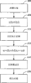
本发明的纳米多孔氧化硅层可使用图2中的PECVD或微波处理室以三层工艺沉积而成,如图5所示。参考图5,步骤300是在该反应器110内放置一衬底,而步骤305是以包含一反应性含硅化合物的等离子体经PECVD工艺沉积成为一阻挡层。依据现有技术公知的方法,在工艺处理室15之内,该沉积步骤305可包含一电容式耦合的等离子体或同时为一感应式和电容式耦合的等离子体。该PECVD沉积过程中通常使用一种惰性气体例如氦辅助产生等离子体。然后于沉积步骤310中,本发明的纳米多孔层更进一步将一含有不稳定性有机基团的硅/氧材料沉积在衬垫层上。 The nanoporous silicon oxide layer of the present invention can be deposited in a three-layer process using the PECVD or microwave processing chamber in FIG. 2 , as shown in FIG. 5 . Referring to FIG. 5 ,
如下文所述,在温度3000℃以下进行等离子体增强沉积可减少刚沉积时膜的应力。 As discussed below, plasma enhanced deposition at temperatures below 3000°C reduces stress on the film as deposited. the
在步骤312内,被沉积的含硅/氧材料经过受控制的热退火处理后即形成多个细微气袋而均匀地散布在层内。下文将详细讨论,依据本发明的实施例,该受控制的热退火处理过程可在多重阶段中以多个不同条件进行,例如先施用热照射后再于电子束下曝露照射。 In
下文中亦将详细讨论,经过热退火处理后,通过释放出刚沉积薄膜中添加的致孔剂可降低薄膜的应力。 As will also be discussed in detail below, thermal annealing reduces film stress by releasing porogens added to the as-deposited film. the
其后,步骤315将一覆盖层沉积在该层上,较佳者宜使用类似于沉积衬垫层的工艺。然后,步骤320将该衬底从反应器110中移出。 Thereafter, step 315 deposits a capping layer on the layer, preferably using a process similar to that used to deposit the liner layer. Then, step 320 removes the substrate from
参考图6A-图6E,该三层工艺提供一PECVD衬垫层400。该衬垫层400作为一层介于后续的纳米多孔层402及其下层的衬底表面404和在衬底表面上形成的多条金属线406、408、410之间的隔离层。该纳米多孔层402是被一层含硅化合物的PECVD覆盖层412所覆盖。此工艺经由使用一储存在CVD反应器110的计算机控制器134的内存220内的计算机程序施行及控制。 Referring to FIGS. 6A-6E , the three-layer process provides a
参考图6A,PECVD衬垫层400是通过引入一反应性含硅化合物和一氧化 气体而沉积在反应器110内。该工艺气体在一等离子体增强环境下反应而在衬底表面404以及多条金属线406、408、410上形成一共形的氧化硅层400。 Referring to FIG. 6A, a
参考图6B,其纳米多孔层402乃由一工艺气体(由硅和多个内含不稳定基的化合物及一氧化气体组成)沉积而成。该工艺气体的流速,在硅及内含不稳定基的化合物约为20至约1000sccm,在氧化气体约为5至约4000sccm。较佳的气体流速,在硅及内含不稳定基的化合物约为50至约500sccm,在氧化气体约为5至约2000sccm。这些流速是针对体积约5.5至6.5公升的处理室。较佳者,在纳米多孔层402沉积期间其反应器110的压力宜维持在约0.2至约5Torr。 Referring to FIG. 6B , the
该纳米多孔层402是先进行固化,如图6CA-图6CB所示,以移除挥发性成分,其后再使覆盖层412沉积,如图6D所示。下文将参照图6CA-图6CB详加说明,该所沉积的低K值膜可在依据本发明实施例的方式的多阶段中固化。此种多阶段固化涉及一热固化步骤,其后接着一电子束固化步骤。或者,在该热固化之前可先进行一电子束固化。 The
或者,固化过程可于惰性气压下在反应器110内进行,并同时将衬底循序渐进地加热至较高温度。该纳米多孔层402可在一缓慢增加的温度下进行热退火处理,以便其气态产物能保持着分散的细微泡沫状态,及/或将该视需要选用的不稳定性有机基团转换成分散的细微气泡停留在经固化的氧化硅薄膜中,有如一较佳的封闭室结构中的多个孔隙。一较佳的退火工艺包含一加热时期,约5分钟,其中包括以约50℃/分钟将温度缓慢地升高至最后温度在约350℃至约400℃。气泡的分散可通过改变温度/时间型态和控制沉积薄膜内不稳定性有机基团的浓度而控制。 Alternatively, the curing process can be performed in the
参考图6D,反应器110沉积覆盖层412,较佳者其材料和沉积方法宜与PECVD衬垫层400相同。参考图6E图,在该覆盖层412沉积之后,该多个沉积层即进一步在一熔炉内或另一处理室中经热退火处理,其温度约200℃至约450℃,以驱除多种残留的挥发性产物,例如水。当然,处理条件会随着对所要求的沉积膜特性而变化。 Referring to FIG. 6D , the
减少低K值薄膜的应力 Reducing Stress in Low-K Films
依据本发明的低K值介电材料可在多个连续的金属导线层之间形成。该 金属层典型地是以较坚硬的材料例如铜或铝形成。由于低K值膜一般而言为软质材料,要将这些实质上具有不同物理性质的膜整合为一在实际上颇为困难。 The low-k dielectric material according to the present invention can be formed between multiple successive layers of metal lines. The metal layer is typically formed of a harder material such as copper or aluminum. Since low-K films are generally soft materials, it is practically difficult to integrate these films with substantially different physical properties into one. the
薄膜应力是决定薄膜强度与其弹性模量的关键因子。因此,生产具有低应力的低-K薄膜至为重要,以有助于使该膜并入半导体结构以及装置之内。 Membrane stress is a key factor in determining the strength of a membrane and its modulus of elasticity. Therefore, it is important to produce low-K thin films with low stress to facilitate their incorporation into semiconductor structures and devices. the
依据本发明的一实施例,薄膜应力小于约20MPa的低K值薄膜可通过化学气相沉积在300℃以下的低温形成。该沉积工艺对热的需求量减少可降低所产生的薄膜的机械应力量。表1提供许多依据本发明实施例形成的含碳氧化硅薄膜的沉积方法的参数摘要。 According to an embodiment of the present invention, a low-K film with a film stress of less than about 20 MPa can be formed by chemical vapor deposition at a low temperature below 300°C. The reduced heat requirement of the deposition process reduces the amount of mechanical stress on the resulting film. Table 1 provides a summary of parameters for a number of deposition methods for carbon-containing silicon oxide films formed in accordance with embodiments of the present invention. the
表1Table 1
压力=6Torr Pressure = 6Torr
面板对晶圆间距=800mils Panel-to-wafer spacing = 800mils
射频功率=500W RF power = 500W
低频功率=200W Low frequency power = 200W
在表1的最后一列中,正数值的应力表示沉积薄膜具有拉伸应力。负数值的应力显示沉积薄膜具有抗压缩应力。依据本发明实施例的薄膜预期将具有应力约20MPa或更低。 In the last column of Table 1, a positive value of stress indicates that the deposited film has tensile stress. Negative values of stress indicate that the deposited film is resistant to compressive stress. Films according to embodiments of the present invention are expected to have stresses of about 20 MPa or less. the
在表1的多个条件下形成的沉积薄膜的应力可与相同组成物在不同条件下形成的沉积薄膜的应力比较。例如,在350℃沉积的类似的碳掺杂氧化硅膜其拉伸应力为56.2Mpa。 The stresses of deposited films formed under various conditions in Table 1 can be compared with the stresses of deposited films formed of the same composition under different conditions. For example, a similar carbon-doped silicon oxide film deposited at 350°C has a tensile stress of 56.2 MPa. the
依据本发明碳掺杂氧化硅膜的实施例并不限于上述特定参数,但可在一条件范围下沉积。下表2总结此条件范围。 Embodiments of carbon-doped silicon oxide films in accordance with the present invention are not limited to the specific parameters described above, but may be deposited under a range of conditions. Table 2 below summarizes this range of conditions. the
表2Table 2
虽然上述讨论针对在低温下形成低K值沉积薄膜以获得低应力,不过依据本发明的实施例并不限于此方法。依据本发明的另一实施例,具有低拉伸应力或甚至抗压缩应力的薄膜可通过与致孔剂共同沉积形成,待致孔剂于其后释出即可使材料的应力减小。 Although the above discussion is directed to forming low K deposited films at low temperature to achieve low stress, embodiments in accordance with the present invention are not limited to this method. According to another embodiment of the present invention, thin films with low tensile stress or even resistance to compressive stress can be formed by co-deposition with a porogen, which is subsequently released to reduce the stress of the material. the
表3示出了一含或不含致孔剂的沉积膜的应力数据。 Table 3 shows the stress data for a deposited film with and without porogen. the
表3table 3
沉积温度=225℃; Deposition temperature = 225°C;
RF功率=1200W; RF power = 1200W;
沉积压力=8Torr; Deposition pressure = 8Torr;
面板对晶圆间距=300mil; Panel-to-wafer spacing = 300mil;
硅前驱物的流速=1200mgm; The flow rate of silicon precursor=1200mgm;
氦的流速=3000sccm; The flow rate of helium=3000sccm;
氧的流速=200sccm; Oxygen flow rate = 200sccm;
表3示出,与添加的致孔剂沉积的碳掺杂氧化硅物,其刚沉积薄膜经过电子束处理后,其应力上的增加实质上少于在相同条件下不含致孔剂的沉积薄膜。 Table 3 shows that the stress increase in as-deposited films of carbon-doped silicon oxide deposited with added porogens after electron beam treatment is substantially less than that deposited without porogens under the same conditions. film. the
所添加的致孔剂其性质亦会影响沉积薄膜最后的应力。图9是添加不同类型致孔剂的薄膜其介电常数对应力的图。第一致孔剂类型(P1)包含环分子,其所占体积大于包含线型分子的第二致孔剂类型(P2)。图9示出与较大致孔剂类型P1沉积的薄膜,其应力小于经后-沉积热退火处理。 The nature of the added porogen also affects the final stress of the deposited film. Figure 9 is a plot of dielectric constant versus stress for films added with different types of porogens. The first porogen type (P1 ) comprises ring molecules which occupy a larger volume than the second porogen type (P2) comprising linear molecules. Figure 9 shows that films deposited with the larger porogen type P1 are less stressed than after post-deposition thermal annealing. the
虽然在热退火处理工艺期间可使用各种电子束辐射源,一典型的装置是EBK处理室,其可购自位于California,Santa Clara的Applied Materials,Inc.。此种大面积的均匀电子源亦已描述于美国专利第5,003,128号中,在此引入全文作为参考。下列专利描述不同特色的电子束处理,在此引入全文作为参考:美国专利第5,468,595号、美国专利第6,132,814号、美国专利第6,204,201号、美国专利第6,207,555号、美国专利第6,271,146号、美国专利第6,319,655号、美国专利第6,407,399号、美国专利第6,150,070号、美国专利第6,218,090号、美国专利第6,195,246号、美国专利第6,218,090号、美国专利第6,426,127号、美国专利第6,340,556号、美国专利第6,358,670号、以及美国专利第6,255,035号、美国专利第6,607,991号、美国专利第6,551,926号、美国专利第6,548,899号、美国专利第6,489,225号、以及美国专利第6,582,777号。E-电子束处理工艺亦在2002年11月22日提交的美国专利申请案号10/302,375(AMAT-7625)发明名称是"Method For Curing Low Dielectric Constant Film By Electron Beam"中详细描述,并在此引入其全文作为参考。 While various sources of electron beam radiation can be used during the thermal annealing process, a typical apparatus is the EBK process chamber, which is commercially available from Applied Materials, Inc. located in Santa Clara, California. Such a large area uniform electron source is also described in US Patent No. 5,003,128, which is incorporated herein by reference in its entirety. The following patents describe electron beam processing of various features and are hereby incorporated by reference in their entirety: US Patent No. 5,468,595, US Patent No. 6,132,814, US Patent No. 6,204,201, US Patent No. 6,207,555, US Patent No. 6,271,146, US Patent No. 6,319,655, US Patent 6,407,399, US Patent 6,150,070, US Patent 6,218,090, US Patent 6,195,246, US Patent 6,218,090, US Patent 6,426,127, US Patent 6,340,556, US Patent 6,358,670 , and US Patent No. 6,255,035, US Patent No. 6,607,991, US Patent No. 6,551,926, US Patent No. 6,548,899, US Patent No. 6,489,225, and US Patent No. 6,582,777. The E-beam processing process is also described in detail in U.S. Patent Application No. 10/302,375 (AMAT-7625) filed on November 22, 2002, entitled "Method For Curing Low Dielectric Constant Film By Electron Beam", and in It is hereby incorporated by reference in its entirety. the
一般而言该电子束在压力约1mTorr至约100mTorr下产生。该电子束可在包含惰性气体的周围环境下形成,其包括:氮、氦、氩、氙;氧化气体,包括:氧;还原气体,包括:氢;混合的氢与氮;氨;或多个此类气体的任何组合。该电子束的电流范围约1mA至约40mA,更佳者约2mA至约20mA。该电子束的覆盖面积约4平方英寸至约700平方英寸。该-电子束工艺装置的操作范围约25℃至约450℃,例如约400℃。 Typically the electron beam is generated at a pressure of about 1 mTorr to about 100 mTorr. The electron beam may be formed in an ambient environment containing an inert gas including: nitrogen, helium, argon, xenon; an oxidizing gas including: oxygen; a reducing gas including: hydrogen; mixed hydrogen and nitrogen; ammonia; Any combination of such gases. The electron beam has a current in the range of about 1 mA to about 40 mA, more preferably about 2 mA to about 20 mA. The electron beam covers an area of about 4 square inches to about 700 square inches. The e-beam processing apparatus has an operating range of about 25°C to about 450°C, for example about 400°C. the
依据本发明实施例的电子束固化处理包含施用于或曝露在剂量少于每平方厘米500微库仑(μC/厘米)之下,较佳者约20以及250μC/厘米Z,例如,约150μC/厘米2。该电子束固化的能量可为约0.5千电子伏特(keV)以及约30 keV,例如介于约2keV及约10keV,例如4keV。 E-beam curing treatments according to embodiments of the present invention include applying or exposing to doses of less than 500 microcoulombs per square centimeter (μC/cm), preferably about 20 and 250 μC/cm, e.g., about 150 μC/cm 2 . The energy of the electron beam curing may be about 0.5 kiloelectron volts (keV) and about 30 keV, such as between about 2 keV and about 10 keV, such as 4 keV.
电子束辐射的施用剂量可加以变化。例如,一介于约10-1000μC/cm2的剂量经发现可使在200毫米以及300毫米衬底上形成的层发生固化。 The administered dose of electron beam radiation can be varied. For example, a dose between about 10-1000 μC/cm 2 was found to cure layers formed on 200 mm as well as 300 mm substrates.
在上述多阶段固化工艺的特定实施例以及图6CA-图6CB图中所示,热固化比电子束固化先发生。此种特定顺序的固化阶段较有利于使该电子束辐射与刚沉积层的表面强烈交互反应,进而促成一表面交联反应而形成坚硬或致密的、交联表层。该表层可阻挡或抑制添加在薄膜中的致孔剂逸出,其将在固化过程中释放。 In the particular embodiment of the multi-stage curing process described above and shown in Figures 6CA-6CB, thermal curing occurs prior to e-beam curing. This specific sequence of curing stages favors a strong interaction of the electron beam radiation with the surface of the as-deposited layer, thereby promoting a surface cross-linking reaction to form a hard or dense, cross-linked surface. This skin blocks or inhibits the escape of porogens added to the film, which will be released during curing. the
不过,本发明实施例并不需要一多阶段固化工艺,其先在热下曝露再以电子束照射。在某些替换性实施例中,其热固化工艺可在电子束照射之后才进行。此种固化步骤顺序交换经证实是有利的,例如,其中由电子束工艺形成的坚硬表面对于材料逸出有正面影响。此种固化步骤顺序交换亦已证实有利于维持高产率,因为热固化步骤通常是整批处理,其可在逐一照射完各个晶圆后再进行。 However, embodiments of the present invention do not require a multi-stage curing process that involves exposure to heat followed by electron beam irradiation. In some alternative embodiments, the thermal curing process may be performed after electron beam irradiation. Such an exchange of the order of the curing steps has proven to be advantageous, for example, where the hard surfaces formed by the electron beam process have a positive effect on material escape. This swapping of the order of the curing steps has also proven beneficial for maintaining high throughput, since the thermal curing step is usually a batch process, which can be performed after each wafer has been irradiated one by one. the
此外,多阶段固化工艺的各个阶段的多个条件可依所欲取得的固化膜的特性而变化。例如,在热退火处理阶段中,可改变其时间和温度变化型态。此外,在电子束固化阶段中,可控制其电子束辐射的施用剂量、能量以及电量。 In addition, various conditions of the various stages of the multi-stage curing process may vary depending on the desired properties of the cured film. For example, during the thermal annealing stage, the time and temperature profile can be changed. In addition, in the electron beam curing stage, the application dose, energy and power of the electron beam radiation can be controlled. the
在依据本发明的实施例中,在多阶段固化工艺期间可变化的另一条件,包括在一个或多个该固化阶段中出现的气体的组成。在一个或多个该固化阶段中出现的气体的多个实施例包括,并不限于,氧分子(O2)、氮分子(N2)、氢分子(H2)、以及稀有气体例如氦(He)。 Another condition that may be varied during a multi-stage curing process in an embodiment in accordance with the invention includes the composition of the gas present during one or more of the curing stages. Examples of gases present during one or more of the curing stages include, without limitation, molecular oxygen (O 2 ), molecular nitrogen (N 2 ), molecular hydrogen (H 2 ), and noble gases such as helium ( He).
上述说明虽相关于多阶段固化工艺利用热能及电子束能,在本发明中却不是绝对必要的。依据某些其它实施例,在不同条件下进行的多重电子束曝光步骤可用以固化低K值沉积膜。 The above description, while related to the multi-stage curing process using thermal energy and electron beam energy, is not absolutely necessary in the present invention. According to certain other embodiments, multiple e-beam exposure steps performed under different conditions may be used to cure low-K deposited films. the
例如,在处理期间,该电子束处理的剂量变异可以由一低值到一高值或由一高值到一低值。或者,该电子束的剂量可在处理期间阶段式上升或下降。同样地,其阴极电压可在处理期间阶段式上升或下降。 For example, the dose of the e-beam treatment may vary from a low value to a high value or from a high value to a low value during processing. Alternatively, the dose of the electron beam can be stepped up or down during treatment. Likewise, its cathode voltage can be stepped up or down during processing. the
双镶嵌结构的沉积 Deposition of dual damascene structures
图7示出了依据本发明制造的较佳双镶嵌结构500,图8A-图8H以概图依序描述制造该结构的方法,其为衬底的剖面图,其上标示有多个本发明的形 成步骤。 Figure 7 shows a preferred dual damascene structure 500 manufactured according to the present invention, and Figures 8A-8H sequentially describe the method of manufacturing the structure in schematic diagrams, which are cross-sectional views of a substrate with multiple inventions marked thereon formation steps. the
图7所示一双镶嵌结构500,其包括一纳米多孔金属间介电层510。依据本发明沉积的该金属间介电层510以及514的介电常数极低,小于3,且常被称为极低k值(或ELK)介电层。第一介电层51O,较佳者由本发明的纳米多孔氧化硅层组成,沉积在衬底502上。该衬底包含多条在触点级衬底材料504上形成的图案化导线506,其上的第一(或衬底)蚀刻中止层508由氧化硅、氮化硅、氮氧化硅、或非结晶形(无定形)氢化碳化硅(BLOkTM)、较佳者氮化硅沉积成层。 FIG. 7 shows a dual damascene structure 500 including a
然后该沉积的介电层510可经过上述多阶段中的热退火处理,释出其不稳定性基团并形成超低K值的纳米微孔材料。 Then the deposited
一由氧化硅、氮化硅、氮氧化硅、或氢化碳化硅(BLOkTM)组成的第二蚀刻中止层512则在第一介电层510之上沉积。 A second
第二介电层514,较佳者由本发明的纳米多孔氧化硅层组成,沉积在该第二蚀刻中止层512之上,而第三蚀刻中止层516则沉积在该第二介电层514之上。沉积之后,第二介电层514亦可通过多阶段的热退火处理使其内部产生纳米微孔,因而降低了该材料的K值。 A
该沉积层经蚀刻而形成一通孔520,接着便以电导金属524,较佳者铜,填充在一保形地沉积在通孔520内的阻挡层522的上方。然后将该结构磨平并在其表面沉积上一层包含氮化硅、氧化硅、氮氧化硅、或氢化碳化硅、较佳者包含氮化硅的覆盖层518。该覆盖层518亦可作为该衬底的蚀刻中止层并相当于后续双镶嵌多层金属互连的第一蚀刻中止层508。 The deposited layer is etched to form a via 520, which is then filled with a
如图8A所示,第一(或衬底)蚀刻中止层508的组成内含氧化硅、氮化硅、氮氧化硅、或非结晶形氢化碳化硅,较佳者氮化硅,其沉积在衬底502上成厚度约 


第二蚀刻中止层512,例如氮氧化硅,沉积在介电层510上,其厚度约 


第三蚀刻中止层516的组成含氧化硅、氮化硅、氮氧化硅、或非结晶形的氢化碳化硅(BLOkTM),较佳者氮化硅,其在第二介电层514上沉积而形成厚度约 


其后该氧化硅层517利用现有技术公知的传统方法蚀刻,较佳者为使用氟碳化合物化学蚀刻的工艺,使第三蚀刻516外露,如图8B所示。最先蚀刻的氧化硅层517确立双镶嵌结构500的开口宽度(或沟槽的宽度)。在该氧化硅层517内形成的该开口的宽度界定了在第二蚀刻中止层514上方形成的双镶嵌结构500的水平互连。然后将残留的光刻胶层521灰化,或干燥移除,以准备进行通孔蚀刻。为了形成双镶嵌结构的接触点或通孔的宽度,于是分别将一第二抗反射涂层519和一光刻胶层521沉积在氧化硅薄层517上,其后再以光刻工艺形成图案使第三蚀刻层516经由通孔的宽度外露,如图8C所示。 Thereafter, the
参考图8D,其第三蚀刻中止层516以及第二介电层514通过沟槽蚀刻而使第二蚀刻中止层512外露。然后使用各向异性蚀刻技术在该第二介电层514到该第二蚀刻中止层512之间蚀刻通孔,其与由该氧化硅层517建立的宽度界定了该金属结构(即导线和接点/通孔);并依该第三蚀刻中止层516、第二介电层514、及该第二蚀刻中止层512的蚀刻通孔宽度自第一介电层510蚀刻到第一蚀刻中止层508,如图8E展示,于是形成了通孔520。用以在第二蚀刻中止层512或第二介电层514形成图案的任何光刻胶剂或ARC材料均使用氧剥除剂或其它适当处理方法予以移除。图8F示出将该第一蚀刻中止层508蚀刻能保护其衬底502,使其下层已图案化的多条金属线506(位于接触级衬底材料504上)外露。该多条图案化的导线506较佳者宜包含一导电性金属例如:铜。然后先用现有技术公知的传统方法清洗该双镶嵌结构500再进行后续的层沉 积程序。 Referring to FIG. 8D , the third
其后以导电性材料例如铝、铜、钨或其多种组合形成该金属结构。由于铜的电阻低(1.7 mW-cm,相较于铝的3.1 mW-cm),因此目前的趋势是使用铜形成多个小型浸蚀孔。较佳地,如第8G图示出,宜先在该金属图案520中保形地沉积上一层适当的阻挡层522,例如氮化钽,以避免铜扩散到周围的硅及/或介电材料中。其后,再使用化学气相沉积、物理气相沉积、电镀,较佳者电/镀,沉积成铜层524,以形成该导电结构。待以铜或其它金属填充该结构后,再用化学机械研磨其表面并覆盖上一覆盖层518,其较佳地内含氮化硅且厚度约为 
实施例 Example
下列实施例描述沉积一纳米多孔氧化硅性薄膜,其中具有分散的微细气体孔隙。本实施例使用一化学气相沉积处理室,更具体地,由CENTURA"DLK"系统制作并由California,Santa Clara的Applied Materials,Inc.出售。 The following examples describe the deposition of a nanoporous silicon oxide film with dispersed microscopic gas pores. This example uses a chemical vapor deposition process chamber, more specifically, fabricated by the CENTURA "DLK" system and manufactured by Applied Materials, Inc. of Santa Clara, California. sell. the
具有含硅及多个致热不稳定性成分(假定的)的硅化合物Silicon compounds with silicon-containing and multiple thermally unstable constituents (presumed)
一基于纳米多孔氧化硅的薄膜在压力1.0 Torr及温度30℃的处理室中以多个反应性气体(其经气化并流入反应器)沉积而成,如下: A thin film based on nanoporous silicon oxide is deposited in a process chamber at a pressure of 1.0 Torr and a temperature of 30°C with reactive gases (which are vaporized and flowed into the reactor), as follows:
甲基硅基-2-呋喃基醚,在 150 sccm Methylsilyl-2-furyl ether at 150 sccm
一氧化二氮(N2O),在 1000 scan Nitrous oxide (N 2 O) at 1000 scan
在进入处理室之前,一氧化二氮是先在微波能2000W下于微波反应作用器内解离。该衬底置于距离气体分布冲洗源600 mil处,且该引入反应性气体历时2分钟。然后将该衬底加热5分钟,使衬底温度以50℃/分钟提高至温度400℃以便使以基于纳米多孔氧化硅的薄膜固化及退火。 Before entering the treatment chamber, the nitrous oxide is first dissociated in the microwave reactor under the microwave energy of 2000W. The substrate was placed 600 mil from the gas distribution flush source, and the reactive gas was introduced for 2 minutes. The substrate was then heated for 5 minutes, increasing the substrate temperature at 50° C./minute to a temperature of 400° C. to cure and anneal the nanoporous silicon oxide-based film. the
具有含硅化合物与致热不稳定性化合物(假定的)的混合物Mixtures with silicon-containing compounds and thermally unstable compounds (presumed)
将一纳米多孔氧化硅为底质的薄膜于压力1.0Torr及温度30℃的处理室中以多个反应性气体(其经气化并流入反应器)沉积而成,如下: A nanoporous silicon oxide-based thin film is deposited in a treatment chamber with a pressure of 1.0 Torr and a temperature of 30°C with a plurality of reactive gases (which are vaporized and flow into the reactor), as follows:
环-1,3,5,7-四亚甲硅基-2,6-二氧-4,8-二亚甲基,在 100sccm Cyclo-1,3,5,7-tetramethylsilylene-2,6-dioxo-4,8-dimethylene at 100sccm
乙烯基-2-呋喃基醚,在 50sccm Vinyl-2-furyl ether at 50 sccm
一氧化二氮(N2O),在 1000sccm Nitrous oxide (N 2 O) at 1000sccm
在进入处理室之前,一氧化二氮是先在微波能2000W下在微波反应作用器内解离。该衬底置于距离气体分布冲洗源600mil处,且引入该反应性气体历时2分钟。然后将该衬底加热5分钟,使衬底温度以50℃/分钟提高至温度400℃以便使以基于纳米多孔氧化硅的薄膜固化及退火。 Before entering the treatment chamber, the nitrous oxide is dissociated in the microwave reactor under the microwave energy of 2000W. The substrate was placed 600 mils from the gas distribution flush source, and the reactive gas was introduced for 2 minutes. The substrate was then heated for 5 minutes, increasing the substrate temperature at 50° C./minute to a temperature of 400° C. to cure and anneal the nanoporous silicon oxide-based film. the
具有含硅及多个致热不稳定性成分的含硅化合物与添加的含硅化合物(假定的)Silicon-containing compounds with silicon-containing and multiple thermally unstable components and added silicon-containing compounds (hypothetical)
将以基于纳米多孔氧化硅的薄膜在压力1.0Torr及温度0℃的处理室中以多个反应性气体(其经气化并流入反应器)沉积而成,如下: A thin film based on nanoporous silicon oxide is deposited in a process chamber with a pressure of 1.0 Torr and a temperature of 0°C with a plurality of reactive gases (which are vaporized and flow into the reactor), as follows:
甲基硅基-2-呋喃基醚,在 100sccm Methylsilyl-2-furyl ether at 100 sccm
环-1,3,5,7-四亚甲硅基-2,6-二氧-4,8-二亚甲基,在 50sccm Cyclo-1,3,5,7-tetramethylsilylene-2,6-dioxo-4,8-dimethylene at 50sccm
一氧化二氮(N2O),在 1000sccm Nitrous oxide (N 2 O) at 1000sccm
进入处理室之前,一氧化二氮是先在微波能2000W下在微波反应作用器内解离。该衬底置于距离气体分布冲洗源600mil处,且引入该反应性气体历时2分钟。然后将该衬底加热5分钟,使衬底温度以50℃/分钟提高至温度400℃以便使以纳米多孔氧化硅为底质的薄膜固化及退火。 Before entering the treatment chamber, the nitrous oxide is first dissociated in the microwave reactor under the microwave energy of 2000W. The substrate was placed 600 mils from the gas distribution flush source, and the reactive gas was introduced for 2 minutes. The substrate was then heated for 5 minutes, increasing the substrate temperature at 50°C/minute to a temperature of 400°C to cure and anneal the nanoporous silicon oxide-based film. the
虽然以上为本发明特定实施例的完整说明,但是仍可使用各种修饰、变化及替代方法。这些等同及替代方法仍包括在本发明的范围内。因此,本发明并不仅限于上述实施例,而是由以下本发明的权利要求书所限定。 While the above is a complete description of specific embodiments of the invention, various modifications, changes, and alternatives may be used. These equivalents and alternatives are still included within the scope of the present invention. Therefore, the present invention is not limited to the above-described embodiments, but is defined by the following claims of the present invention. the
Claims (15)
Applications Claiming Priority (5)
| Application Number | Priority Date | Filing Date | Title |
|---|---|---|---|
| US60431604P | 2004-08-24 | 2004-08-24 | |
| US60/604,316 | 2004-08-24 | ||
| US11/149,826 | 2005-06-10 | ||
| US11/149,826 US7422776B2 (en) | 2004-08-24 | 2005-06-10 | Low temperature process to produce low-K dielectrics with low stress by plasma-enhanced chemical vapor deposition (PECVD) |
| PCT/US2005/030302 WO2006024017A1 (en) | 2004-08-24 | 2005-08-24 | Low temperature process to produce low-k dielectrics with low stress by plasma-enhanced chemical vapor deposition (pecvd) |
Publications (2)
| Publication Number | Publication Date |
|---|---|
| CN101065834A CN101065834A (en) | 2007-10-31 |
| CN101065834B true CN101065834B (en) | 2010-12-08 |
Family
ID=35542287
Family Applications (1)
| Application Number | Title | Priority Date | Filing Date |
|---|---|---|---|
| CN2005800340479A Expired - Fee Related CN101065834B (en) | 2004-08-24 | 2005-08-24 | A Low-Temperature Process for Fabricating Low-K Dielectrics with Low Stress by Plasma-Enhanced Chemical Vapor Deposition |
Country Status (5)
| Country | Link |
|---|---|
| US (1) | US7422776B2 (en) |
| KR (1) | KR101221582B1 (en) |
| CN (1) | CN101065834B (en) |
| TW (1) | TWI332240B (en) |
| WO (1) | WO2006024017A1 (en) |
Families Citing this family (63)
| Publication number | Priority date | Publication date | Assignee | Title |
|---|---|---|---|---|
| US6734533B2 (en) * | 2002-05-30 | 2004-05-11 | Intel Corporation | Electron-beam treated CDO films |
| US20060081557A1 (en) | 2004-10-18 | 2006-04-20 | Molecular Imprints, Inc. | Low-k dielectric functional imprinting materials |
| US7217648B2 (en) * | 2004-12-22 | 2007-05-15 | Taiwan Semiconductor Manufacturing Company, Ltd. | Post-ESL porogen burn-out for copper ELK integration |
| US7501354B2 (en) * | 2005-01-18 | 2009-03-10 | Applied Materials, Inc. | Formation of low K material utilizing process having readily cleaned by-products |
| US7892648B2 (en) * | 2005-01-21 | 2011-02-22 | International Business Machines Corporation | SiCOH dielectric material with improved toughness and improved Si-C bonding |
| US7378318B2 (en) * | 2005-08-18 | 2008-05-27 | International Business Machines Corporation | System and method for ensuring migratability of circuits by masking portions of the circuits while improving performance of other portions of the circuits |
| US7381659B2 (en) * | 2005-11-22 | 2008-06-03 | International Business Machines Corporation | Method for reducing film stress for SiCOH low-k dielectric materials |
| JP2008010441A (en) * | 2006-06-27 | 2008-01-17 | Toshiba Corp | Method for forming silicon oxide film |
| US7297376B1 (en) | 2006-07-07 | 2007-11-20 | Applied Materials, Inc. | Method to reduce gas-phase reactions in a PECVD process with silicon and organic precursors to deposit defect-free initial layers |
| US7723226B2 (en) * | 2007-01-17 | 2010-05-25 | Taiwan Semiconductor Manufacturing Company, Ltd. | Interconnects containing bilayer porous low-k dielectrics using different porogen to structure former ratio |
| US7670924B2 (en) * | 2007-01-29 | 2010-03-02 | Applied Materials, Inc. | Air gap integration scheme |
| US20080182403A1 (en) * | 2007-01-26 | 2008-07-31 | Atif Noori | Uv curing of pecvd-deposited sacrificial polymer films for air-gap ild |
| US8084357B2 (en) * | 2007-04-11 | 2011-12-27 | United Microelectronics Corp. | Method for manufacturing a dual damascene opening comprising a trench opening and a via opening |
| US20090283310A1 (en) * | 2007-04-11 | 2009-11-19 | Wei-Chih Chen | Multi cap layer and manufacturing method thereof |
| US7858532B2 (en) | 2007-08-06 | 2010-12-28 | United Microelectronics Corp. | Dielectric layer structure and manufacturing method thereof |
| US8092861B2 (en) | 2007-09-05 | 2012-01-10 | United Microelectronics Corp. | Method of fabricating an ultra dielectric constant (K) dielectric layer |
| US7879683B2 (en) * | 2007-10-09 | 2011-02-01 | Applied Materials, Inc. | Methods and apparatus of creating airgap in dielectric layers for the reduction of RC delay |
| US20090093100A1 (en) * | 2007-10-09 | 2009-04-09 | Li-Qun Xia | Method for forming an air gap in multilevel interconnect structure |
| US9778562B2 (en) * | 2007-11-21 | 2017-10-03 | Canon Nanotechnologies, Inc. | Porous template and imprinting stack for nano-imprint lithography |
| US20090324849A1 (en) * | 2007-12-28 | 2009-12-31 | Varian Semiconductor Equipement Associates, Inc. | Method for sealing pores in a porous substrate |
| US20100072671A1 (en) * | 2008-09-25 | 2010-03-25 | Molecular Imprints, Inc. | Nano-imprint lithography template fabrication and treatment |
| US8470188B2 (en) * | 2008-10-02 | 2013-06-25 | Molecular Imprints, Inc. | Nano-imprint lithography templates |
| US20100104852A1 (en) * | 2008-10-23 | 2010-04-29 | Molecular Imprints, Inc. | Fabrication of High-Throughput Nano-Imprint Lithography Templates |
| US7858503B2 (en) * | 2009-02-06 | 2010-12-28 | Applied Materials, Inc. | Ion implanted substrate having capping layer and method |
| US8616873B2 (en) * | 2010-01-26 | 2013-12-31 | Molecular Imprints, Inc. | Micro-conformal templates for nanoimprint lithography |
| US20110189329A1 (en) * | 2010-01-29 | 2011-08-04 | Molecular Imprints, Inc. | Ultra-Compliant Nanoimprint Lithography Template |
| US9028924B2 (en) * | 2010-03-25 | 2015-05-12 | Novellus Systems, Inc. | In-situ deposition of film stacks |
| US8741394B2 (en) | 2010-03-25 | 2014-06-03 | Novellus Systems, Inc. | In-situ deposition of film stacks |
| TWI403612B (en) * | 2011-04-22 | 2013-08-01 | Archers Inc | Apparatus of plasma-enhanced chemical vapor deposition |
| KR101690392B1 (en) * | 2011-12-20 | 2016-12-27 | 인텔 코포레이션 | Conformal low temperature hermetic dielectric diffusion barriers |
| US9165788B2 (en) | 2012-04-06 | 2015-10-20 | Novellus Systems, Inc. | Post-deposition soft annealing |
| US9117668B2 (en) | 2012-05-23 | 2015-08-25 | Novellus Systems, Inc. | PECVD deposition of smooth silicon films |
| US9234276B2 (en) | 2013-05-31 | 2016-01-12 | Novellus Systems, Inc. | Method to obtain SiC class of films of desired composition and film properties |
| US10325773B2 (en) | 2012-06-12 | 2019-06-18 | Novellus Systems, Inc. | Conformal deposition of silicon carbide films |
| US12334332B2 (en) | 2012-06-12 | 2025-06-17 | Lam Research Corporation | Remote plasma based deposition of silicon carbide films using silicon-containing and carbon-containing precursors |
| US10832904B2 (en) | 2012-06-12 | 2020-11-10 | Lam Research Corporation | Remote plasma based deposition of oxygen doped silicon carbide films |
| US20180347035A1 (en) | 2012-06-12 | 2018-12-06 | Lam Research Corporation | Conformal deposition of silicon carbide films using heterogeneous precursor interaction |
| US9388491B2 (en) | 2012-07-23 | 2016-07-12 | Novellus Systems, Inc. | Method for deposition of conformal films with catalysis assisted low temperature CVD |
| US9490163B2 (en) * | 2012-08-31 | 2016-11-08 | Taiwan Semiconductor Manufacturing Company Limited | Tapered sidewall conductive lines and formation thereof |
| US9362133B2 (en) | 2012-12-14 | 2016-06-07 | Lam Research Corporation | Method for forming a mask by etching conformal film on patterned ashable hardmask |
| CN103077884B (en) * | 2013-01-14 | 2015-09-30 | 武汉新芯集成电路制造有限公司 | A kind of method solving film separation |
| US10297442B2 (en) | 2013-05-31 | 2019-05-21 | Lam Research Corporation | Remote plasma based deposition of graded or multi-layered silicon carbide film |
| US8895415B1 (en) | 2013-05-31 | 2014-11-25 | Novellus Systems, Inc. | Tensile stressed doped amorphous silicon |
| TW201535513A (en) | 2014-02-18 | 2015-09-16 | 應用材料股份有限公司 | Low-k dielectric layer with reduced dielectric constant and mechanical properties |
| US20160314964A1 (en) * | 2015-04-21 | 2016-10-27 | Lam Research Corporation | Gap fill using carbon-based films |
| US20170125241A1 (en) * | 2015-10-30 | 2017-05-04 | Applied Materials, Inc. | Low temp single precursor arc hard mask for multilayer patterning application |
| US9786491B2 (en) | 2015-11-12 | 2017-10-10 | Asm Ip Holding B.V. | Formation of SiOCN thin films |
| KR102378021B1 (en) | 2016-05-06 | 2022-03-23 | 에이에스엠 아이피 홀딩 비.브이. | Formation of SiOC thin films |
| US10002787B2 (en) | 2016-11-23 | 2018-06-19 | Lam Research Corporation | Staircase encapsulation in 3D NAND fabrication |
| JP7118512B2 (en) | 2017-04-07 | 2022-08-16 | アプライド マテリアルズ インコーポレイテッド | Gap filling using reactive annealing |
| CN110546302B (en) | 2017-05-05 | 2022-05-27 | Asm Ip 控股有限公司 | Plasma enhanced deposition method for controlled formation of oxygen-containing films |
| KR102659317B1 (en) * | 2017-09-12 | 2024-04-18 | 어플라이드 머티어리얼스, 인코포레이티드 | Apparatus and methods for manufacturing semiconductor structures using a protective barrier layer |
| KR20190065962A (en) * | 2017-12-04 | 2019-06-12 | 에이에스엠 아이피 홀딩 비.브이. | UNIFORM DEPOSITION OF SiOC ON DIELECTRIC AND METAL SURFACES |
| US10840087B2 (en) | 2018-07-20 | 2020-11-17 | Lam Research Corporation | Remote plasma based deposition of boron nitride, boron carbide, and boron carbonitride films |
| CN109119574B (en) * | 2018-08-15 | 2021-06-18 | 苏州大学 | Porous lithium-ion battery separator based on cross-linked and linear polymer and its preparation method and application |
| KR20220056248A (en) | 2018-10-19 | 2022-05-04 | 램 리써치 코포레이션 | Doped or undoped silicon carbide deposition and remote hydrogen plasma exposure for gapfill |
| CN110129769B (en) | 2019-05-17 | 2021-05-14 | 江苏菲沃泰纳米科技股份有限公司 | Hydrophobic low dielectric constant film and method for preparing same |
| CN110158052B (en) * | 2019-05-17 | 2021-05-14 | 江苏菲沃泰纳米科技股份有限公司 | Low dielectric constant film and preparation method thereof |
| JP7465287B2 (en) | 2019-06-08 | 2024-04-10 | アプライド マテリアルズ インコーポレイテッド | Low-k dielectrics with self-forming barrier layers |
| CN110797255B (en) * | 2019-10-14 | 2022-10-28 | 长江存储科技有限责任公司 | Thin film stack structure, three-dimensional memory and preparation method thereof |
| US11990369B2 (en) | 2021-08-20 | 2024-05-21 | Applied Materials, Inc. | Selective patterning with molecular layer deposition |
| EP4402300A1 (en) * | 2021-10-13 | 2024-07-24 | Versum Materials US, LLC | Alkoxysilanes and dense organosilica films made therefrom |
| US12154766B2 (en) * | 2022-06-07 | 2024-11-26 | Applied Materials, Inc. | Ion source having different modes of operation |
Citations (7)
| Publication number | Priority date | Publication date | Assignee | Title |
|---|---|---|---|---|
| EP1119035A2 (en) * | 2000-01-18 | 2001-07-25 | Applied Materials, Inc. | Method for depositing a low dielectric constant film |
| US6410462B1 (en) * | 2000-05-12 | 2002-06-25 | Sharp Laboratories Of America, Inc. | Method of making low-K carbon doped silicon oxide |
| US6465372B1 (en) * | 1999-08-17 | 2002-10-15 | Applied Materials, Inc. | Surface treatment of C-doped SiO2 film to enhance film stability during O2 ashing |
| US6663973B1 (en) * | 1997-10-24 | 2003-12-16 | Canon, Usa, Inc. | Low dielectric constant materials prepared from photon or plasma assisted chemical vapor deposition and transport polymerization of selected compounds |
| CN1464536A (en) * | 2002-06-19 | 2003-12-31 | 台湾积体电路制造股份有限公司 | Method for forming low dielectric constant material and product thereof |
| EP1420439A2 (en) * | 2002-11-14 | 2004-05-19 | Air Products And Chemicals, Inc. | Non-thermal process for forming porous low dielectric constant films |
| CN1514477A (en) * | 2002-12-31 | 2004-07-21 | ̨������·����ɷ�����˾ | Semiconductor device using nitrogen-free dielectric etch stop layer and process thereof |
Family Cites Families (38)
| Publication number | Priority date | Publication date | Assignee | Title |
|---|---|---|---|---|
| US5000113A (en) | 1986-12-19 | 1991-03-19 | Applied Materials, Inc. | Thermal CVD/PECVD reactor and use for thermal chemical vapor deposition of silicon dioxide and in-situ multi-step planarized process |
| US5003128A (en) | 1988-11-08 | 1991-03-26 | Yvan Grondin | Electrical switch and outlets protecting cover for painting |
| US5468595A (en) | 1993-01-29 | 1995-11-21 | Electron Vision Corporation | Method for three-dimensional control of solubility properties of resist layers |
| MY113904A (en) | 1995-05-08 | 2002-06-29 | Electron Vision Corp | Method for curing spin-on-glass film utilizing electron beam radiation |
| US6607991B1 (en) | 1995-05-08 | 2003-08-19 | Electron Vision Corporation | Method for curing spin-on dielectric films utilizing electron beam radiation |
| US6042994A (en) | 1998-01-20 | 2000-03-28 | Alliedsignal Inc. | Nanoporous silica dielectric films modified by electron beam exposure and having low dielectric constant and low water content |
| US6303523B2 (en) | 1998-02-11 | 2001-10-16 | Applied Materials, Inc. | Plasma processes for depositing low dielectric constant films |
| US6177143B1 (en) | 1999-01-06 | 2001-01-23 | Allied Signal Inc | Electron beam treatment of siloxane resins |
| US6255035B1 (en) | 1999-03-17 | 2001-07-03 | Electron Vision Corporation | Method of creating optimal photoresist structures used in the manufacture of metal T-gates for high-speed semiconductor devices |
| US6150070A (en) | 1999-03-17 | 2000-11-21 | Alliedsignal Inc. | Method of creating optimal profile in single layer photoresist |
| US6207555B1 (en) | 1999-03-17 | 2001-03-27 | Electron Vision Corporation | Electron beam process during dual damascene processing |
| US6218090B1 (en) | 1999-03-17 | 2001-04-17 | Electron Vision Corporation | Method of creating controlled discontinuity between photoresist and substrate for improving metal lift off |
| US6195246B1 (en) | 1999-03-30 | 2001-02-27 | Electron Vision Corporation | Electrostatic chuck having replaceable dielectric cover |
| US6551926B1 (en) | 1999-06-09 | 2003-04-22 | Electron Vision Corporation | Electron beam annealing of metals, alloys, nitrides and silicides |
| US6319655B1 (en) | 1999-06-11 | 2001-11-20 | Electron Vision Corporation | Modification of 193 nm sensitive photoresist materials by electron beam exposure |
| US6204201B1 (en) | 1999-06-11 | 2001-03-20 | Electron Vision Corporation | Method of processing films prior to chemical vapor deposition using electron beam processing |
| US6489225B1 (en) | 1999-06-11 | 2002-12-03 | Electron Vision Corporation | Method for controlling dopant profiles and dopant activation by electron beam processing |
| US6340556B1 (en) | 1999-08-04 | 2002-01-22 | Electron Vision Corporation | Tailoring of linewidth through electron beam post exposure |
| EP1077480B1 (en) | 1999-08-17 | 2008-11-12 | Applied Materials, Inc. | Method and apparatus to enhance properties of Si-O-C low K films |
| US6271146B1 (en) | 1999-09-30 | 2001-08-07 | Electron Vision Corporation | Electron beam treatment of fluorinated silicate glass |
| US6407399B1 (en) | 1999-09-30 | 2002-06-18 | Electron Vision Corporation | Uniformity correction for large area electron source |
| US6358670B1 (en) | 1999-12-28 | 2002-03-19 | Electron Vision Corporation | Enhancement of photoresist plasma etch resistance via electron beam surface cure |
| US6426127B1 (en) | 1999-12-28 | 2002-07-30 | Electron Vision Corporation | Electron beam modification of perhydrosilazane spin-on glass |
| US6582777B1 (en) | 2000-02-17 | 2003-06-24 | Applied Materials Inc. | Electron beam modification of CVD deposited low dielectric constant materials |
| US6511923B1 (en) * | 2000-05-19 | 2003-01-28 | Applied Materials, Inc. | Deposition of stable dielectric films |
| US6790789B2 (en) | 2000-10-25 | 2004-09-14 | International Business Machines Corporation | Ultralow dielectric constant material as an intralevel or interlevel dielectric in a semiconductor device and electronic device made |
| US6632478B2 (en) * | 2001-02-22 | 2003-10-14 | Applied Materials, Inc. | Process for forming a low dielectric constant carbon-containing film |
| US6890850B2 (en) * | 2001-12-14 | 2005-05-10 | Applied Materials, Inc. | Method of depositing dielectric materials in damascene applications |
| US6806203B2 (en) * | 2002-03-18 | 2004-10-19 | Applied Materials Inc. | Method of forming a dual damascene structure using an amorphous silicon hard mask |
| US7056560B2 (en) * | 2002-05-08 | 2006-06-06 | Applies Materials Inc. | Ultra low dielectric materials based on hybrid system of linear silicon precursor and organic porogen by plasma-enhanced chemical vapor deposition (PECVD) |
| US6797643B2 (en) * | 2002-10-23 | 2004-09-28 | Applied Materials Inc. | Plasma enhanced CVD low k carbon-doped silicon oxide film deposition using VHF-RF power |
| US6914014B2 (en) * | 2003-01-13 | 2005-07-05 | Applied Materials, Inc. | Method for curing low dielectric constant film using direct current bias |
| US7208389B1 (en) * | 2003-03-31 | 2007-04-24 | Novellus Systems, Inc. | Method of porogen removal from porous low-k films using UV radiation |
| US20040253378A1 (en) | 2003-06-12 | 2004-12-16 | Applied Materials, Inc. | Stress reduction of SIOC low k film by addition of alkylenes to OMCTS based processes |
| US7148154B2 (en) | 2003-08-20 | 2006-12-12 | Asm Japan K.K. | Method of forming silicon-containing insulation film having low dielectric constant and low film stress |
| US7094713B1 (en) * | 2004-03-11 | 2006-08-22 | Novellus Systems, Inc. | Methods for improving the cracking resistance of low-k dielectric materials |
| US7166531B1 (en) * | 2005-01-31 | 2007-01-23 | Novellus Systems, Inc. | VLSI fabrication processes for introducing pores into dielectric materials |
| US7135402B2 (en) * | 2005-02-01 | 2006-11-14 | Taiwan Semiconductor Manufacturing Company, Ltd. | Sealing pores of low-k dielectrics using CxHy |
-
2005
- 2005-06-10 US US11/149,826 patent/US7422776B2/en not_active Expired - Lifetime
- 2005-08-24 WO PCT/US2005/030302 patent/WO2006024017A1/en not_active Ceased
- 2005-08-24 CN CN2005800340479A patent/CN101065834B/en not_active Expired - Fee Related
- 2005-08-24 TW TW094128998A patent/TWI332240B/en not_active IP Right Cessation
- 2005-08-24 KR KR1020077006747A patent/KR101221582B1/en not_active Expired - Lifetime
Patent Citations (7)
| Publication number | Priority date | Publication date | Assignee | Title |
|---|---|---|---|---|
| US6663973B1 (en) * | 1997-10-24 | 2003-12-16 | Canon, Usa, Inc. | Low dielectric constant materials prepared from photon or plasma assisted chemical vapor deposition and transport polymerization of selected compounds |
| US6465372B1 (en) * | 1999-08-17 | 2002-10-15 | Applied Materials, Inc. | Surface treatment of C-doped SiO2 film to enhance film stability during O2 ashing |
| EP1119035A2 (en) * | 2000-01-18 | 2001-07-25 | Applied Materials, Inc. | Method for depositing a low dielectric constant film |
| US6410462B1 (en) * | 2000-05-12 | 2002-06-25 | Sharp Laboratories Of America, Inc. | Method of making low-K carbon doped silicon oxide |
| CN1464536A (en) * | 2002-06-19 | 2003-12-31 | 台湾积体电路制造股份有限公司 | Method for forming low dielectric constant material and product thereof |
| EP1420439A2 (en) * | 2002-11-14 | 2004-05-19 | Air Products And Chemicals, Inc. | Non-thermal process for forming porous low dielectric constant films |
| CN1514477A (en) * | 2002-12-31 | 2004-07-21 | ̨������·����ɷ�����˾ | Semiconductor device using nitrogen-free dielectric etch stop layer and process thereof |
Also Published As
| Publication number | Publication date |
|---|---|
| TWI332240B (en) | 2010-10-21 |
| TW200610054A (en) | 2006-03-16 |
| US7422776B2 (en) | 2008-09-09 |
| KR101221582B1 (en) | 2013-01-14 |
| KR20070057857A (en) | 2007-06-07 |
| WO2006024017A1 (en) | 2006-03-02 |
| CN101065834A (en) | 2007-10-31 |
| US20060043591A1 (en) | 2006-03-02 |
Similar Documents
| Publication | Publication Date | Title |
|---|---|---|
| CN101065834B (en) | A Low-Temperature Process for Fabricating Low-K Dielectrics with Low Stress by Plasma-Enhanced Chemical Vapor Deposition | |
| JP4918190B2 (en) | Very low dielectric constant plasma enhanced CVD film | |
| US7611996B2 (en) | Multi-stage curing of low K nano-porous films | |
| CN1938833B (en) | Method and interconnect structure for promoting adhesion of porous low-k film to underlying barrier layer | |
| US20080105978A1 (en) | Method for forming an ultra low dielectric film by forming an organosilicon matrix and large porogens as a template for increased porosity | |
| US7501354B2 (en) | Formation of low K material utilizing process having readily cleaned by-products |
Legal Events
| Date | Code | Title | Description |
|---|---|---|---|
| C06 | Publication | ||
| PB01 | Publication | ||
| C10 | Entry into substantive examination | ||
| SE01 | Entry into force of request for substantive examination | ||
| C14 | Grant of patent or utility model | ||
| GR01 | Patent grant | ||
| C56 | Change in the name or address of the patentee | ||
| CP01 | Change in the name or title of a patent holder |
Address after: American California Patentee after: Applied Materials Inc. Address before: American California Patentee before: Applied Materials Inc. |
|
| CF01 | Termination of patent right due to non-payment of annual fee |
Granted publication date: 20101208 Termination date: 20140824 |
|
| EXPY | Termination of patent right or utility model |