CN100578773C - Memory module systems and methods - Google Patents
Memory module systems and methods Download PDFInfo
- Publication number
- CN100578773C CN100578773C CN200680026190A CN200680026190A CN100578773C CN 100578773 C CN100578773 C CN 100578773C CN 200680026190 A CN200680026190 A CN 200680026190A CN 200680026190 A CN200680026190 A CN 200680026190A CN 100578773 C CN100578773 C CN 100578773C
- Authority
- CN
- China
- Prior art keywords
- substrate
- flexible
- csps
- circuit
- memory module
- Prior art date
- Legal status (The legal status is an assumption and is not a legal conclusion. Google has not performed a legal analysis and makes no representation as to the accuracy of the status listed.)
- Expired - Fee Related
Links
Images


Classifications
-
- H—ELECTRICITY
- H05—ELECTRIC TECHNIQUES NOT OTHERWISE PROVIDED FOR
- H05K—PRINTED CIRCUITS; CASINGS OR CONSTRUCTIONAL DETAILS OF ELECTRIC APPARATUS; MANUFACTURE OF ASSEMBLAGES OF ELECTRICAL COMPONENTS
- H05K1/00—Printed circuits
- H05K1/02—Details
- H05K1/11—Printed elements for providing electric connections to or between printed circuits
- H05K1/117—Pads along the edge of rigid circuit boards, e.g. for pluggable connectors
-
- H10W70/40—
-
- G—PHYSICS
- G11—INFORMATION STORAGE
- G11C—STATIC STORES
- G11C5/00—Details of stores covered by group G11C11/00
- G11C5/02—Disposition of storage elements, e.g. in the form of a matrix array
- G11C5/04—Supports for storage elements, e.g. memory modules; Mounting or fixing of storage elements on such supports
-
- H—ELECTRICITY
- H05—ELECTRIC TECHNIQUES NOT OTHERWISE PROVIDED FOR
- H05K—PRINTED CIRCUITS; CASINGS OR CONSTRUCTIONAL DETAILS OF ELECTRIC APPARATUS; MANUFACTURE OF ASSEMBLAGES OF ELECTRICAL COMPONENTS
- H05K1/00—Printed circuits
- H05K1/02—Details
- H05K1/14—Structural association of two or more printed circuits
- H05K1/147—Structural association of two or more printed circuits at least one of the printed circuits being bent or folded, e.g. by using a flexible printed circuit
-
- H—ELECTRICITY
- H05—ELECTRIC TECHNIQUES NOT OTHERWISE PROVIDED FOR
- H05K—PRINTED CIRCUITS; CASINGS OR CONSTRUCTIONAL DETAILS OF ELECTRIC APPARATUS; MANUFACTURE OF ASSEMBLAGES OF ELECTRICAL COMPONENTS
- H05K1/00—Printed circuits
- H05K1/18—Printed circuits structurally associated with non-printed electric components
- H05K1/189—Printed circuits structurally associated with non-printed electric components characterised by the use of a flexible or folded printed circuit
-
- H—ELECTRICITY
- H05—ELECTRIC TECHNIQUES NOT OTHERWISE PROVIDED FOR
- H05K—PRINTED CIRCUITS; CASINGS OR CONSTRUCTIONAL DETAILS OF ELECTRIC APPARATUS; MANUFACTURE OF ASSEMBLAGES OF ELECTRICAL COMPONENTS
- H05K1/00—Printed circuits
- H05K1/02—Details
- H05K1/14—Structural association of two or more printed circuits
- H05K1/141—One or more single auxiliary printed circuits mounted on a main printed circuit, e.g. modules, adapters
-
- H—ELECTRICITY
- H05—ELECTRIC TECHNIQUES NOT OTHERWISE PROVIDED FOR
- H05K—PRINTED CIRCUITS; CASINGS OR CONSTRUCTIONAL DETAILS OF ELECTRIC APPARATUS; MANUFACTURE OF ASSEMBLAGES OF ELECTRICAL COMPONENTS
- H05K2201/00—Indexing scheme relating to printed circuits covered by H05K1/00
- H05K2201/05—Flexible printed circuits [FPCs]
- H05K2201/056—Folded around rigid support or component
-
- H—ELECTRICITY
- H05—ELECTRIC TECHNIQUES NOT OTHERWISE PROVIDED FOR
- H05K—PRINTED CIRCUITS; CASINGS OR CONSTRUCTIONAL DETAILS OF ELECTRIC APPARATUS; MANUFACTURE OF ASSEMBLAGES OF ELECTRICAL COMPONENTS
- H05K2201/00—Indexing scheme relating to printed circuits covered by H05K1/00
- H05K2201/09—Shape and layout
- H05K2201/09209—Shape and layout details of conductors
- H05K2201/09372—Pads and lands
- H05K2201/09445—Pads for connections not located at the edge of the PCB, e.g. for flexible circuits
-
- H—ELECTRICITY
- H05—ELECTRIC TECHNIQUES NOT OTHERWISE PROVIDED FOR
- H05K—PRINTED CIRCUITS; CASINGS OR CONSTRUCTIONAL DETAILS OF ELECTRIC APPARATUS; MANUFACTURE OF ASSEMBLAGES OF ELECTRICAL COMPONENTS
- H05K2201/00—Indexing scheme relating to printed circuits covered by H05K1/00
- H05K2201/10—Details of components or other objects attached to or integrated in a printed circuit board
- H05K2201/10007—Types of components
- H05K2201/10159—Memory
-
- H—ELECTRICITY
- H05—ELECTRIC TECHNIQUES NOT OTHERWISE PROVIDED FOR
- H05K—PRINTED CIRCUITS; CASINGS OR CONSTRUCTIONAL DETAILS OF ELECTRIC APPARATUS; MANUFACTURE OF ASSEMBLAGES OF ELECTRICAL COMPONENTS
- H05K2201/00—Indexing scheme relating to printed circuits covered by H05K1/00
- H05K2201/10—Details of components or other objects attached to or integrated in a printed circuit board
- H05K2201/10007—Types of components
- H05K2201/10189—Non-printed connector
-
- H—ELECTRICITY
- H05—ELECTRIC TECHNIQUES NOT OTHERWISE PROVIDED FOR
- H05K—PRINTED CIRCUITS; CASINGS OR CONSTRUCTIONAL DETAILS OF ELECTRIC APPARATUS; MANUFACTURE OF ASSEMBLAGES OF ELECTRICAL COMPONENTS
- H05K2201/00—Indexing scheme relating to printed circuits covered by H05K1/00
- H05K2201/10—Details of components or other objects attached to or integrated in a printed circuit board
- H05K2201/10431—Details of mounted components
- H05K2201/1056—Metal over component, i.e. metal plate over component mounted on or embedded in PCB
-
- H—ELECTRICITY
- H05—ELECTRIC TECHNIQUES NOT OTHERWISE PROVIDED FOR
- H05K—PRINTED CIRCUITS; CASINGS OR CONSTRUCTIONAL DETAILS OF ELECTRIC APPARATUS; MANUFACTURE OF ASSEMBLAGES OF ELECTRICAL COMPONENTS
- H05K2201/00—Indexing scheme relating to printed circuits covered by H05K1/00
- H05K2201/10—Details of components or other objects attached to or integrated in a printed circuit board
- H05K2201/10613—Details of electrical connections of non-printed components, e.g. special leads
- H05K2201/10621—Components characterised by their electrical contacts
- H05K2201/10734—Ball grid array [BGA]; Bump grid array
-
- H—ELECTRICITY
- H05—ELECTRIC TECHNIQUES NOT OTHERWISE PROVIDED FOR
- H05K—PRINTED CIRCUITS; CASINGS OR CONSTRUCTIONAL DETAILS OF ELECTRIC APPARATUS; MANUFACTURE OF ASSEMBLAGES OF ELECTRICAL COMPONENTS
- H05K2203/00—Indexing scheme relating to apparatus or processes for manufacturing printed circuits covered by H05K3/00
- H05K2203/15—Position of the PCB during processing
- H05K2203/1572—Processing both sides of a PCB by the same process; Providing a similar arrangement of components on both sides; Making interlayer connections from two sides
-
- H—ELECTRICITY
- H05—ELECTRIC TECHNIQUES NOT OTHERWISE PROVIDED FOR
- H05K—PRINTED CIRCUITS; CASINGS OR CONSTRUCTIONAL DETAILS OF ELECTRIC APPARATUS; MANUFACTURE OF ASSEMBLAGES OF ELECTRICAL COMPONENTS
- H05K3/00—Apparatus or processes for manufacturing printed circuits
- H05K3/0058—Laminating printed circuit boards onto other substrates, e.g. metallic substrates
- H05K3/0061—Laminating printed circuit boards onto other substrates, e.g. metallic substrates onto a metallic substrate, e.g. a heat sink
-
- H—ELECTRICITY
- H05—ELECTRIC TECHNIQUES NOT OTHERWISE PROVIDED FOR
- H05K—PRINTED CIRCUITS; CASINGS OR CONSTRUCTIONAL DETAILS OF ELECTRIC APPARATUS; MANUFACTURE OF ASSEMBLAGES OF ELECTRICAL COMPONENTS
- H05K3/00—Apparatus or processes for manufacturing printed circuits
- H05K3/46—Manufacturing multilayer circuits
- H05K3/4688—Composite multilayer circuits, i.e. comprising insulating layers having different properties
- H05K3/4691—Rigid-flexible multilayer circuits comprising rigid and flexible layers, e.g. having in the bending regions only flexible layers
Landscapes
- Engineering & Computer Science (AREA)
- Microelectronics & Electronic Packaging (AREA)
- Combinations Of Printed Boards (AREA)
- Coupling Device And Connection With Printed Circuit (AREA)
Abstract
提供一种电路模块,其中两个辅助基板(21A、21B)或卡或刚性柔性组件的刚性部分(16B)组装有集成电路(IC)。辅助基板与柔性电路相连。柔性电路的一侧呈现出适于连接到边缘连接器(12)的触点。柔性电路(20)包在优选为金属的基板的边缘周围,以将所述两个辅助基板中一个设置在基板的第一侧上,而将所述辅助基板中的另一个设置在基板的第二侧上。
A circuit module is provided in which two auxiliary substrates (21A, 21B) or a rigid portion (16B) of a card or rigid-flexible assembly are assembled with an integrated circuit (IC). The auxiliary substrates are connected to a flexible circuit. One side of the flexible circuit presents contacts suitable for connection to an edge connector (12). The flexible circuit (20) is wrapped around the edge of a substrate, preferably metal, so that one of the two auxiliary substrates is disposed on a first side of the substrate, and the other auxiliary substrate is disposed on a second side of the substrate.
Description
技术领域 technical field
本发明涉及用于制造高密度电路模块的系统和方法。The present invention relates to systems and methods for fabricating high density circuit modules.
背景技术 Background technique
公知的DIMM(双列直插存储器模块)板已经以各种形式使用了多年,以提供存储器扩展。典型的DIMM包括常规PCB(印刷电路板),其两侧安装有存储器件和支持数字逻辑器件。通常通过将DIMM的具有触点的接口边插入到边缘连接器插槽中而将DIMM安装在主计算机系统中。采用DIMM的系统为这种器件提供有限的空间,常规的基于DIMM的方案通常只能提供中等的存储器扩展量。The well known DIMM (Dual Inline Memory Module) boards have been used in various forms for many years to provide memory expansion. A typical DIMM consists of a regular PCB (printed circuit board) with memory devices and supporting digital logic devices mounted on both sides. A DIMM is typically installed in a host computer system by inserting the interface edge of the DIMM having contacts into an edge connector slot. Systems using DIMMs offer limited space for such devices, and conventional DIMM-based solutions typically provide only moderate amounts of memory expansion.
随着芯片尺寸增大,常规DIMM上有限的可用表面积限制了在根据常规DIMM技术设计的存储器扩展模块上可以承载的器件数量。此外,随着总线速度的提高,每个通道的可以通过基于DIMM的方案而被可靠寻址的器件更少了。例如,利用无缓冲DIMM使用SDRAM-100总线协议可以对每个通道的288个IC或器件进行寻址。利用DDR-200总线协议,可以对每个通道的大约144个器件进行寻址。利用DDR2-400总线协议,仅仅可以对每个通道的72个器件进行寻址。这一限制导致开发出具有缓冲的C/A和数据的全缓冲DIMM(FB-DIMM),其中可以对每个通道的288个器件进行寻址。对于FB-DIMM而言,不仅容量增加了,而且管脚数从以前所需的大约240个管脚下降到大约69个信号管脚。As chip sizes increase, the limited surface area available on conventional DIMMs limits the number of devices that can be carried on a memory expansion module designed according to conventional DIMM technology. Additionally, as bus speeds increase, fewer devices per channel can be reliably addressed by DIMM-based schemes. For example, 288 ICs or devices per channel can be addressed using the SDRAM-100 bus protocol using unbuffered DIMMs. Using the DDR-200 bus protocol, approximately 144 devices per channel can be addressed. Using the DDR2-400 bus protocol, only 72 devices per channel can be addressed. This limitation led to the development of fully buffered DIMMs (FB-DIMMs) with buffered C/A and data, where 288 devices per channel can be addressed. For FB-DIMMs, not only has the capacity increased, but the number of pins has dropped from about 240 pins previously required to about 69 signal pins.
预计FB-DIMM电路方案可以提供高达约192吉字节的实际母板存储器容量,其具有六个通道,每个通道8个DIMM,每个DIMM两个存储体,使用一吉比特DRAM。该方案也应当适于下一代技术,并应当表现出显著的向下兼容能力。The FB-DIMM circuit scheme is expected to provide up to about 192 gigabytes of actual motherboard memory capacity, with six channels of 8 DIMMs per channel, two banks per DIMM, using one gigabit of DRAM. The scheme should also be suitable for next-generation technologies and should exhibit significant downward compatibility.
然而,这一改善也带来一些成本,并将最终受自身制约。采用FB-DIMM的系统的基本原理基于点到点或串行寻址方案,而不是用于控制无缓冲DIMM寻址的并行多点接口(multi-drop interface)。即,一个DIMM与存储器控制器是点到点的关系,并且每一个DIMM与相邻的DIMM是点到点关系。因而,随着总线速度的提高,总线上的DIMM数量将会减少,因为从控制器到“最后的”DIMM的点到点连接链所导致的不连续性实际上随着速度的增大而被放大。However, this improvement also comes with some costs and will ultimately be self-limiting. The fundamentals of systems using FB-DIMMs are based on point-to-point or serial addressing schemes, rather than the parallel multi-drop interface used to control unbuffered DIMM addressing. That is, one DIMM has a point-to-point relationship with the memory controller, and each DIMM has a point-to-point relationship with an adjacent DIMM. Thus, as the bus speed increases, the number of DIMMs on the bus will decrease because the discontinuity caused by the chain of point-to-point connections from the controller to the "last" DIMM is actually eliminated as the speed increases. enlarge.
已知有很多用于提高DIMM和类似模块的容量的技术和系统。例如,可以在单个IC封装中封装多个管芯。然后可以使DIMM模块组装有这种多管芯器件。然而,多管芯制造和测试较为复杂,在多管芯封装中几乎没有存储器和其他电路设计可用。Many techniques and systems are known for increasing the capacity of DIMMs and similar modules. For example, multiple dies may be packaged in a single IC package. DIMM modules can then be populated with such multi-die devices. However, multi-die fabrication and testing are complex, and few memory and other circuit designs are available in multi-die packages.
还有人曾使用子卡来提高DIMM的容量,但是更好的构造策略和减少的部件数量会改善这种模块及其制造成本。提高DIMM容量的更有效的方法,无论是否是全缓冲的,都在计算系统中找到了价值。Daughter cards have also been used to increase the capacity of DIMMs, but better construction strategies and reduced part counts would improve such modules and their manufacturing costs. More efficient methods of increasing DIMM capacity, fully buffered or not, are finding value in computing systems.
发明内容 Contents of the invention
提供一种电路模块,其中两个辅助基板或卡或刚性柔性组件组装有集成电路(IC)。辅助基板或刚性柔性组件的刚性部分与柔性电路的柔性部分相连。柔性电路的一侧呈现出适于连接到边缘连接器的触点。柔性电路包在优选为金属的基板的边缘周围,以将两个辅助基板中的一个设置在基板的第一侧上,并将辅助基板中的另一个设置在基板的第二侧上。A circuit module is provided in which two auxiliary substrates or cards or rigid-flex assemblies are populated with integrated circuits (ICs). The rigid portion of the secondary substrate or rigid-flex assembly is connected to the flexible portion of the flex circuit. One side of the flex circuit presents contacts suitable for connection to the edge connector. The flexible circuit is wrapped around the edge of the preferably metallic substrate to place one of the two auxiliary substrates on the first side of the substrate and the other of the auxiliary substrates on the second side of the substrate.
附图说明 Description of drawings
图1为根据本发明优选实施例设计的模块的示图;Fig. 1 is the diagram of the module designed according to the preferred embodiment of the present invention;
图2示出可以在本发明优选实施例中采用的辅助基板;Figure 2 shows an auxiliary substrate that may be employed in a preferred embodiment of the invention;
图3示出根据本发明优选实施例设计的柔性电路的第一侧;Figure 3 shows a first side of a flexible circuit designed in accordance with a preferred embodiment of the present invention;
图4示出根据本发明优选实施例设计的模块的截面图;Figure 4 shows a cross-sectional view of a module designed according to a preferred embodiment of the present invention;
图5为图4中由A标识的区域的放大图;Figure 5 is an enlarged view of the area identified by A in Figure 4;
图6为图4中由B标识的区域的放大图;Figure 6 is an enlarged view of the area identified by B in Figure 4;
图7为在本发明的替代性的优选实施例中采用的柔性电路的分解截面图;Figure 7 is an exploded cross-sectional view of a flexible circuit employed in an alternative preferred embodiment of the present invention;
图8为本发明的另一实施例;Fig. 8 is another embodiment of the present invention;
图9示出本发明的又一实施例;Fig. 9 shows yet another embodiment of the present invention;
图10示出根据本发明实施例的模块;Figure 10 shows a module according to an embodiment of the invention;
图11为在本发明的可选实施例中使用的示例性连接器的放大图;Figure 11 is an enlarged view of an exemplary connector used in an alternative embodiment of the invention;
图12示出具有两部分基板的又一实施例。Figure 12 shows yet another embodiment with a two-part substrate.
具体实施方式 Detailed ways
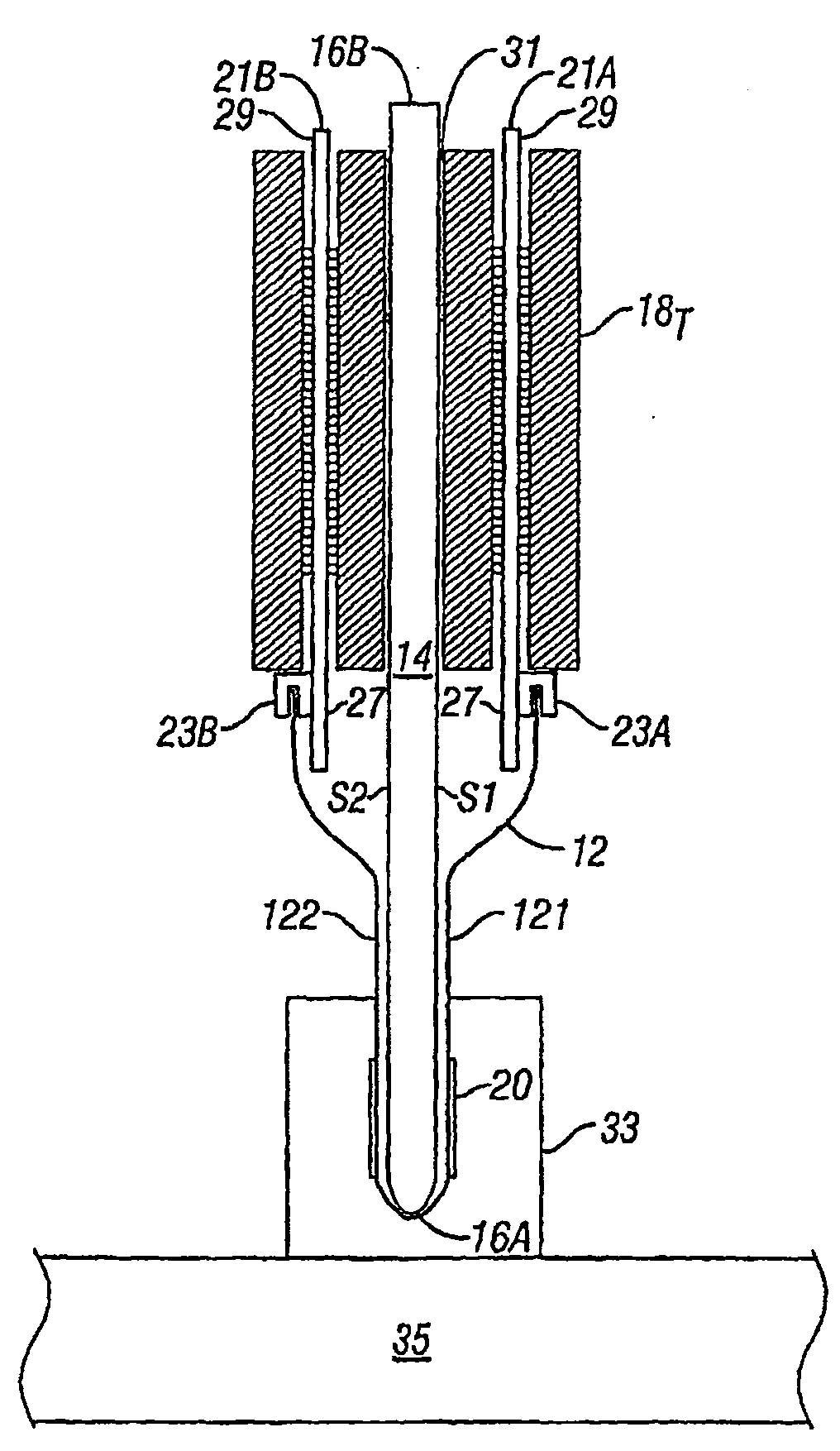
图1示出根据本发明优选实施例的模块10。在主基板14的每一侧上设置辅助基板21,在所述辅助基板21上设有IC 18,在所示的实施例中,所述IC 18为芯片级封装存储器件。沿着主基板14的下边缘示出柔性电路12的一部分。沿着柔性电路12的侧8设置扩展或边缘连接器模块触点20,并且在优选实施例中,一些扩展或边缘连接器模块触点20将呈现在模块10的两侧中的每一侧上,尽管在一些实施例中边缘连接器或模块触点20可以仅位于模块10的一侧上。例如,主基板14可以是PCB材料或F4板,或者,在优选实施例中,它是金属材料,例如金属合金或混合物、或者铜或铝,例如以实现更有效的热管理。Figure 1 shows a
为了本公开的目的,术语芯片级或“CSP”应当是指具有阵列封装的任何功能的集成电路,所述阵列封装通过分布在封装或管芯的整个主表面上的触点(例如常常被实施为“突起”或“球”)提供至一个或多个管芯的连接。CSP不是指带引线的器件,其通过从封装(例如TSOP)周边中的至少一边露出的引线提供至封装内的集成电路的连接。For the purposes of this disclosure, the term chip-scale or "CSP" shall refer to an integrated circuit having any function of an array package that is implemented via contacts distributed over the entire major surface of the package or die (such as often implemented A "bump" or "ball") provides connections to one or more dies. A CSP does not refer to a leaded device that provides connection to the integrated circuit within the package through leads exposed from at least one side of the package's (eg, TSOP's) perimeter.
可以以采用封装形式或未封装形式的带引线的器件或CSP器件或其他器件的方式来使用本发明的实施例,然而在使用CSP这一术语时,都应当采用以上对CSP的定义。因此,尽管CSP排除了带引线的器件,对CSP的引用应当被宽泛地理解为包括多种阵列器件(不仅限于存储器),无论是管芯尺寸的还是其他尺寸,例如BGA和微型BGA,以及倒装芯片。在理解本公开后本领域的技术人员将会认识到,可以设计本发明的一些实施例以采用IC的叠置,每个设置在示例性附图中标识IC 18的位置。Embodiments of the present invention may be used with leaded or CSP devices or other devices in packaged or unpackaged form, however the above definition of CSP should be used whenever the term CSP is used. Thus, while CSP excludes leaded devices, references to CSP should be read broadly to include a variety of array devices (not limited to memory), whether die-sized or otherwise, such as BGA and micro-BGA, and inverted Install the chip. Those skilled in the art will recognize after understanding the present disclosure that some embodiments of the invention may be designed to employ stacking of ICs, each arrangement identifying the location of
在被示为单个IC 18的封装中可以包括多个集成电路管芯。在该实施例中,根据本发明使用存储器IC来提供存储器扩展板或模块。然而,各种其他实施例可以采用多种集成电路和其他部件。作为非限制性实例列表,这些种类可以包括微处理器、FPGA、RF收发器电路和数字逻辑,或其他可以从增强的高密度电路板或模块性能受益的电路或系统。因此,所述的IC 18的多个实例可以是具有第一主要功能或类型的器件,例如存储器,而诸如所示电路19的其他器件可以是具有第二主要功能或类型的器件,例如信号缓冲器,其的一个例子是用于模块的全缓冲电路设计中的高级存储缓冲器(“AMB”)。IC 19例如还可以是热传感器,其生成可以在确定模块10的热积累或温度时使用的一个或多个信号。集成电路19例如还可以是用于图形处理的图形处理器。当电路19为热传感器时,它可以安装在辅助基板21相对于模块10的主基板14的内表面上,以能够更精确地感测模块10的热状态。图1和图2所示的电路19应当被理解为不是按照精确比例绘制的,而仅仅是示意性的。Multiple integrated circuit dies may be included in the package shown as a
图2示出组装有一组具有第一主要功能的IC 18的示例性辅助基板21。如将要所说明的那样,可以设计几个实施例,其将呈现出各自组装有一组CSP的第一和第二辅助基板。辅助基板21可以由多种材料构成,通常,由PCB材料构成,尽管可以将本领域公知的其他材料用作根据本发明的辅助基板。例如,辅助基板21可以由集成的刚性柔性结构的刚性部分和柔性部分提供,所述刚性部分为IC18、IC 19和诸如寄存器和PLL的其他电路提供安装区域,所述柔性部分在主基板14附近通过或延伸到安装在主基板14上的柔性边缘连接器。当辅助基板21与柔性电路12分立但却连接时,例如,通过柔性边缘连接器23(例如图2所示的柔性边缘连接器),IC 18、IC 19和其他支持电路之间的连接网络是电可到达的。辅助基板21可以展现出IC 18的单排设置,或者在可选实施例中,可以展现出在一侧或两侧上存在一排以上的IC。FIG. 2 shows an exemplary
图3示出在构造根据本发明优选实施例的模块中使用的优选柔性电路12(“柔性电路”、“柔性电路系统”“柔性的电路”、“柔性的电路系统”)的侧8。在整个柔性的电路(flexible circuit)上,柔性的电路系统(flexible circuitry)保持为基本连续和可控阻抗电路。这与现有技术相反,现有技术提供从卡边缘连接器焊盘通过刚性PCB延伸到用于IC的通孔或表面安装焊盘的电路。当信号通过作为电路中的连接器的一部分的导线或总线条(bus bar)时,这会造成阻抗不连续。Figure 3 shows
柔性电路12优选由通过一个或多个柔性基板层所支撑的一个或多个导电层制成,如本文中图7所进一步详述的那样。柔性电路12的整体可以是柔性的,或如本领域技术人员所知道的那样,可以使柔性电路12在某些区域中是柔性的,以便顺应所需的形状或弯曲,并使其在其他区域中是刚性的,以便提供辅助基板21的平面安装表面。在这种利用刚性柔性组件的情况下,应当视为其包括辅助基板和柔性电路,在本文图8中将其标识为组合了柔性电路和辅助基板的单个附图标记。The
图3示出柔性电路12的第一或外侧8。柔性电路12具有两行(CR1和CR2)模块触点20,线“L”在中间。线L沿着柔性电路12的中线,但未必一定如此。触点20适于插入在电路板插槽中,在优选实施例中所述插槽例如为边缘连接器。当相对于主基板14的边缘16A折叠柔性电路12时,图1所示的侧8位于模块10的外侧。柔性电路12的相对侧例如在图4的折叠结构中位于内侧。虽然没有示出,但是本领域技术人员在没有对柔性电路12的另一侧进行文字描述的情况下也能够理解柔性电路12的双侧性质。在几种所示的模块10的结构中,柔性电路12的另一侧或“第二侧”位于内侧,从而柔性电路12的第二侧比侧8更接近基板14,柔性电路12设置在其附近。其他实施例可以具有其他数量的设置成一行或多行或其他方式的触点,且可以仅有一行这样的触点,它可以在线L的一侧而不是分布在L的两侧或接近柔性电路的边缘。在图3中与柔性电路12一起示出柔性边缘触点25,在所示的实施例中,被标为25A的那些柔性边缘触点通过柔性边缘连接器23A与第一辅助基板21A以及该辅助基板上承载的电路(例如IC 18和19)连接,而被标为25B的那些则通过柔性边缘连接器23B与第二辅助基板21B连接。在图4中进一步示出该实施例的设置。FIG. 3 shows the first or
其他实施例可以采用并非矩形而可以是正方形的柔性电路12,在这种情况下,周边边缘尺寸相等,或者,柔性电路12可以是其他方便的形状,以适于制造或所关注应用的规格细节。Other embodiments may employ a
图4为根据本发明优选实施例设计的模块10的截面图。模块10上组装有IC 18,其具有顶表面18T和底表面18B。基板或支持结构14具有作为末端出现在图4的示图中的第一和第二周边边缘16A和16B。基板或支持结构14通常具有第一和第二横向侧S1和S2。柔性电路12包在或经过基板14的周边边缘16A的周围,在所示的实施例中,所述基板14提供了通用DIMM形状因数(例如由JEDEC标准MO-256定义的形状因数)的基本形状。这样将柔性电路12的第一部分(121)设置成接近基板14的侧S1,而将柔性电路12的第二部分(122)设置成接近基板14的侧S2。Fig. 4 is a cross-sectional view of a
所示的模块10展现出第一辅助基板21A和第二辅助基板21B,所述辅助基板中的每一个都在其相应侧27和29中的每一侧上组装有多个IC 18,侧27相对于模块10处在内侧。尽管在该实施例中,所述的四个IC相对成对地附着到相应的辅助基板,这并非限制性的,可以以其他布置,例如交错或偏移布置,来连接更多的IC。可以采用在图4中部分示出的粘合剂31来改善至基板14的热能传递,所述基板14优选为金属或其他导热材料。如同柔性边缘连接器23A和23B一样在图4中示出柔性电路12的模块触点20。The illustrated
以如下设计的方式设置柔性电路12的模块触点20:使其安装在电路板卡边缘连接器或插槽中,例如安装在图4所示的安装在母板35上的边缘连接器33中,并连接到连接器中相应的触点(未示出)。边缘连接器33可以是各种其他装置例如通用计算机和笔记本的一部分。所示的基板14和柔性电路12在厚度上可以变化,并未按比例绘制以便简化附图。所示的基板14具有这样的厚度,使得在与柔性电路12以及用于将柔性电路12附着到基板14的粘合剂组装时,在模块触点20之间测得的厚度落在为配合连接器33指定的范围内。在一些其他实施例中,如本领域技术人员所知的那样,可以将柔性电路12包在周边边缘16B的周围。The
图5示出示例性模块10的放大部分。尽管所示的模块触点20从柔性电路12的表面突出,所述柔性电路12在主基板14的边缘16A周围通过。然而,这不是限制性的,其他实施例可以具有齐平的触点或在柔性电路12的表面高度之下的触点。主基板14从柔性电路12的后面以如下设计的方式支撑模块触点20:提供插入到插槽中所需的机械形式。尽管所示的基板14具有均匀的厚度,但这不是限制性的,在其他实施例中基板14的厚度或表面可以以多种方式变化,以便例如提供更薄的模块。FIG. 5 shows an enlarged portion of
在周边边缘16A附近或在周边边缘16B附近,基板14的形状也可以不同于均匀的锥形。作为非限制性的实例,所示实施例中的基板14优选由诸如铝或铜的金属制成,或者在热管理不大成问题的情况下,由诸如FR4(4型阻燃剂)环氧树脂叠层、PTFE(聚四氟乙烯)或塑料的材料制成。在另一实施例中,可以通过使用在两侧上具有铜层的FR4而将多项技术的有利特征结合起来,以提供从熟知的材料设计出来的基板14,所述材料可以提供热传导或接地面。基板14也可以在边缘16B处展现出延伸,以帮助热管理。Near
用于有效地组装如本文所述和所示的电路模块10的一种有利方法如下。包括柔性边缘连接器23的第一和第二辅助基板21在相应的辅助基板侧27和29上组装有诸如IC 18的电路。使柔性电路12在基板14附近,并且通过将内侧IC 18的上侧18T粘着到主基板14而将辅助基板21A和21B附着到主基板14,并使柔性边缘触点25与相应的柔性边缘连接器23相配合。One advantageous method for efficiently assembling a
图6示出示例性模块10的一部分的放大细节,图中示出在模块10的两侧的每一侧上包括两排IC 18。所示的第一和第二辅助基板21A和21B在其相应侧27和29上组装有IC 18。该放大图示出IC 18的CSP触点37。所示的柔性边缘连接器23A和23B分别与柔性边缘触点25A和25B相配合。本领域技术人员将会注意到,尽管难以操作,但是在一些可选模块10中,柔性电路也可以在基板14的顶边缘16B之上通过,以降低在边缘16A周围通过的柔性电路中的信号密度。FIG. 6 shows an enlarged detail of a portion of an
图7为根据本发明的一个实施例的柔性电路12的截面的分解图。所示的柔性电路12具有四个导电层701-704和七个绝缘层705-711。所述的层数仅仅是在一个优选实施例中所用的层数,可以采用其他层数和层的设置。在一些实施例中甚至可以使用单个导电层柔性电路12,但具有一个以上导电层的柔性电路被证明更适于本发明的更为复杂的实施例。FIG. 7 is an exploded view of a cross-section of the
顶导电层701和其他导电层优选由诸如铜或合金110的导电金属制成。在这种设置中,导电层701、702和704表示信号迹线712,其利用柔性电路12形成各种连接。这些层还可以表示用于接地、电源或参考电压的导电平面。The top
在该实施例中,内侧导电层702表示连接到安装在辅助基板21上的各种器件的迹线以及它们之间的迹线。所示导电层中的任何一个的功能可以在功能上与导电层中的其他导电层互换。内侧导电层703表示接地面,可以将其分开以为预寄存器地址信号提供VDD返回。内侧导电层703还可以表示其他平面和迹线。在该实施例中,除了所示的迹线之外,底部导电层704处的区域(floods)或平面还提供VREF和地。In this embodiment, the inner
在该实施例中,绝缘层705和711是例如可以沉积在相邻导电层上的电介质焊接掩模层。其他实施例可以不具有这种粘合剂电介质层。绝缘层706、708和710优选为由聚酰亚胺制成的柔性电介质基板层。然而,任何适当的柔性电路都可以在本发明中使用,图7的示图应当被理解为仅仅是可以被用作柔性电路12的更复杂的柔性电路结构中的一个的实例。In this embodiment, insulating
图8示出根据本发明的实施例。在图8所示的实施例中,辅助基板21A和21B为柔性组件12RF的一部分。柔性组件12RF包括辅助基板部分21A和21B以及相应的柔性部分12FA和12FB,虽然它们优选是一体的,但被分开标识以示出柔性组件的第一和第二柔性部分,其分别最靠近基板14的侧S1和S2。如图所示,优选地,在使柔性组件12RF处在基板14的边缘16A附近时,柔性部分12FA和12FB是一体的。如本领域的技术人员所知的那样,使用单个的柔性组件之所以具有制造优点尤其是在于:单个的柔性电路是通过组件而不是两个部件来处理的。Figure 8 shows an embodiment according to the invention. In the embodiment shown in FIG. 8, the
图9示出根据本发明的另一实施例。图9所示的模块10采用被标识为具有两个部分12A和12B的柔性电路12,如被标识为“S”的区域所示,通过将柔性边缘焊盘焊接到辅助基板而将所述两个部分12A和12B附着到相应的第一和第二辅助基板21A和21B。柔性电路12在基板14的边缘16A周围通过。如图9的示图所示,来自基板14的扩展部分16T增加基板14的质量和辐射表面积,从而给模块10更大的机会来减小热能积累。Fig. 9 shows another embodiment according to the invention. The
图10示出根据本发明的另一实施例。在如图10所示的模块10中,利用连接器40将辅助基板21连接到主基板14的模块触点20。Fig. 10 shows another embodiment according to the invention. In the
图11是图10所示的实施例中的主基板14的侧S2上的连接器40B周围区域的放大图。所示的连接器40B具有彼此配合并为信号提供受控阻抗路径的第一部分401和第二部分402。可以获得的诸如连接器40的连接器具有各种类型和结构,这样的连接器的一个示例性提供商是Molex。FIG. 11 is an enlarged view of the area around the
图12示出根据本发明的模块10的可选实施例。如图12所示,采用导电引线42将辅助基板21连接到主基板14被标识为14B的部分。在示图中,基板14被画成在区域“C”处结合的部分14A和14B。用于结合两个材料不同的部分的技术是本领域所公知的,示出的所建议的一种选择是区域C处的部分14A和14B之间的舌和槽布置,然而本领域技术人员在理解本说明书之后会认识到,可以使用许多技术中的任何一种技术来将部分14A和14B结合成基板14。部分14B由诸如FR4的板构成,并且包括用于将导电引线42连接到触点20的导电迹线或区域,所述触点20优选设计成插入在边缘连接器中。基板14的部分14A由诸如铝或铜或铜合金的金属构成。所示的模块10具有扩展部分16T,其提高了模块10的热性能,尤其是在部分14A为金属的实施例中。Figure 12 shows an alternative embodiment of a
本发明可以有利地用于各种应用和环境,例如,通过被设置在母板扩展槽中以提供增大的存储容量同时占用更少的插槽而在诸如服务器和笔记本计算机的计算机中使用。如本领域技术人员在理解本说明书之后所认识到的那样,使用两个多排实施例或单排实施例都可以有这样的优点。The present invention can be advantageously used in various applications and environments, for example, in computers such as servers and notebook computers by being disposed in motherboard expansion slots to provide increased storage capacity while occupying fewer slots. Such advantages may be achieved using either the multi-row embodiment or the single-row embodiment, as will be appreciated by those skilled in the art after understanding this specification.
尽管已经详细地对本发明进行了说明,但对于本领域技术人员而言显而易见的是,在不背离本发明的实质精神和范围的情况下,可以获得很多采用各种特定形式并反映出变化、替换和修改的实施例。因此,所述实施例是示例性的,而不限制权利要求书的范围。Although the present invention has been described in detail, it will be apparent to those skilled in the art that there can be many modifications, variations, and substitutions in various specific forms without departing from the true spirit and scope of the invention. and modified examples. Accordingly, the described embodiments are exemplary and do not limit the scope of the claims.
Claims (25)
Applications Claiming Priority (2)
| Application Number | Priority Date | Filing Date | Title |
|---|---|---|---|
| US11/131,835 US20060261449A1 (en) | 2005-05-18 | 2005-05-18 | Memory module system and method |
| US11/131,835 | 2005-05-18 |
Publications (2)
| Publication Number | Publication Date |
|---|---|
| CN101223639A CN101223639A (en) | 2008-07-16 |
| CN100578773C true CN100578773C (en) | 2010-01-06 |
Family
ID=37431714
Family Applications (1)
| Application Number | Title | Priority Date | Filing Date |
|---|---|---|---|
| CN200680026190A Expired - Fee Related CN100578773C (en) | 2005-05-18 | 2006-02-09 | Memory module systems and methods |
Country Status (5)
| Country | Link |
|---|---|
| US (3) | US20060261449A1 (en) |
| JP (1) | JP2008541293A (en) |
| KR (1) | KR20080006016A (en) |
| CN (1) | CN100578773C (en) |
| WO (1) | WO2006124085A2 (en) |
Families Citing this family (41)
| Publication number | Priority date | Publication date | Assignee | Title |
|---|---|---|---|---|
| US7254036B2 (en) | 2004-04-09 | 2007-08-07 | Netlist, Inc. | High density memory module using stacked printed circuit boards |
| US7443023B2 (en) * | 2004-09-03 | 2008-10-28 | Entorian Technologies, Lp | High capacity thin module system |
| US20060050492A1 (en) * | 2004-09-03 | 2006-03-09 | Staktek Group, L.P. | Thin module system and method |
| US7511968B2 (en) * | 2004-09-03 | 2009-03-31 | Entorian Technologies, Lp | Buffered thin module system and method |
| US7616452B2 (en) | 2004-09-03 | 2009-11-10 | Entorian Technologies, Lp | Flex circuit constructions for high capacity circuit module systems and methods |
| US7442050B1 (en) | 2005-08-29 | 2008-10-28 | Netlist, Inc. | Circuit card with flexible connection for memory module with heat spreader |
| US20070158811A1 (en) * | 2006-01-11 | 2007-07-12 | James Douglas Wehrly | Low profile managed memory component |
| US7508058B2 (en) * | 2006-01-11 | 2009-03-24 | Entorian Technologies, Lp | Stacked integrated circuit module |
| US7608920B2 (en) * | 2006-01-11 | 2009-10-27 | Entorian Technologies, Lp | Memory card and method for devising |
| US7605454B2 (en) * | 2006-01-11 | 2009-10-20 | Entorian Technologies, Lp | Memory card and method for devising |
| US7619893B1 (en) | 2006-02-17 | 2009-11-17 | Netlist, Inc. | Heat spreader for electronic modules |
| US7429788B2 (en) * | 2006-03-08 | 2008-09-30 | Microelectronics Assembly Technologies, Inc. | Thin multichip flex-module |
| US7520781B2 (en) * | 2006-03-08 | 2009-04-21 | Microelectronics Assembly Technologies | Thin multichip flex-module |
| US7393226B2 (en) * | 2006-03-08 | 2008-07-01 | Microelectronics Assembly Technologies, Inc. | Thin multichip flex-module |
| US7394149B2 (en) * | 2006-03-08 | 2008-07-01 | Microelectronics Assembly Technologies, Inc. | Thin multichip flex-module |
| US8018723B1 (en) | 2008-04-30 | 2011-09-13 | Netlist, Inc. | Heat dissipation for electronic modules |
| US8334704B2 (en) * | 2009-02-20 | 2012-12-18 | Apple Inc. | Systems and methods for providing a system-on-a-substrate |
| US9204550B2 (en) * | 2011-09-30 | 2015-12-01 | Smart Modular Technologies, Inc. | Extended capacity memory system with load relieved memory and method of manufacture thereof |
| KR102245293B1 (en) | 2012-04-10 | 2021-04-28 | 이덱스 바이오메트릭스 아사 | Biometric Sensing |
| KR102046988B1 (en) * | 2012-05-25 | 2019-11-20 | 삼성전자 주식회사 | Printed Circuit Board(PCB) having low insertion-force, manufacturing method thereof and system comprising the same |
| USD716310S1 (en) * | 2012-06-09 | 2014-10-28 | Apple, Inc. | Electronic device |
| GB2526565B (en) * | 2014-05-28 | 2016-06-29 | Ibm | Assembly of printed circuit boards |
| US10178786B2 (en) | 2015-05-04 | 2019-01-08 | Honeywell International Inc. | Circuit packages including modules that include at least one integrated circuit |
| CN105390150A (en) * | 2015-12-02 | 2016-03-09 | 西安华为技术有限公司 | Storage device |
| KR102449193B1 (en) * | 2015-12-04 | 2022-09-29 | 삼성전자주식회사 | Memory package including buffer, expandable memory module and multi-module memory system |
| TWD189071S (en) * | 2017-02-17 | 2018-03-11 | 三星電子股份有限公司 | Ssd storage device |
| TWD189069S (en) * | 2017-02-17 | 2018-03-11 | 三星電子股份有限公司 | Ssd storage device |
| TWD189066S (en) * | 2017-02-17 | 2018-03-11 | 三星電子股份有限公司 | Ssd storage device |
| TWD189067S (en) * | 2017-02-17 | 2018-03-11 | 三星電子股份有限公司 | Ssd storage device |
| TWD189070S (en) * | 2017-02-17 | 2018-03-11 | 三星電子股份有限公司 | Ssd storage device |
| TWD190983S (en) * | 2017-02-17 | 2018-06-11 | 三星電子股份有限公司 | Ssd storage device |
| TWD189068S (en) * | 2017-02-17 | 2018-03-11 | 三星電子股份有限公司 | Ssd storage device |
| TWD189065S (en) * | 2017-02-17 | 2018-03-11 | 三星電子股份有限公司 | Ssd storage device |
| CN107507635A (en) * | 2017-09-05 | 2017-12-22 | 郑州云海信息技术有限公司 | A kind of double-deck interconnection mainboard SSD hard disks |
| US10249972B1 (en) * | 2017-09-22 | 2019-04-02 | Google Llc | Vertically stacking circuit board connectors |
| JP6597810B2 (en) * | 2018-02-02 | 2019-10-30 | 日本電気株式会社 | Mounting structure, structural component, and manufacturing method of mounting structure |
| USD869469S1 (en) * | 2018-04-09 | 2019-12-10 | Samsung Electronics Co., Ltd. | SSD storage device |
| USD869470S1 (en) * | 2018-04-09 | 2019-12-10 | Samsung Electronics Co., Ltd. | SSD storage device |
| USD967823S1 (en) * | 2019-05-06 | 2022-10-25 | Dell Products L.P. | Information handling system storage device |
| FI20205672A1 (en) | 2020-06-25 | 2021-12-26 | Epec Oy | Electronic device and method for forming an electronic device |
| WO2023139872A1 (en) * | 2022-01-24 | 2023-07-27 | パナソニックIpマネジメント株式会社 | Storage medium module |
Citations (3)
| Publication number | Priority date | Publication date | Assignee | Title |
|---|---|---|---|---|
| US6157541A (en) * | 1997-12-30 | 2000-12-05 | Siemens Aktiengesellschaft | Stack arrangement for two semiconductor memory chips and printed board for accepting a plurality of such stack arrangements |
| US6357023B1 (en) * | 1998-04-08 | 2002-03-12 | Kingston Technology Co. | Connector assembly for testing memory modules from the solder-side of a PC motherboard with forced hot air |
| US6521984B2 (en) * | 2000-11-07 | 2003-02-18 | Mitsubishi Denki Kabushiki Kaisha | Semiconductor module with semiconductor devices attached to upper and lower surface of a semiconductor substrate |
Family Cites Families (117)
| Publication number | Priority date | Publication date | Assignee | Title |
|---|---|---|---|---|
| US3372310A (en) * | 1965-04-30 | 1968-03-05 | Radiation Inc | Universal modular packages for integrated circuits |
| US3436604A (en) * | 1966-04-25 | 1969-04-01 | Texas Instruments Inc | Complex integrated circuit array and method for fabricating same |
| US3654394A (en) * | 1969-07-08 | 1972-04-04 | Gordon Eng Co | Field effect transistor switch, particularly for multiplexing |
| US3727064A (en) * | 1971-03-17 | 1973-04-10 | Monsanto Co | Opto-isolator devices and method for the fabrication thereof |
| US3718842A (en) * | 1972-04-21 | 1973-02-27 | Texas Instruments Inc | Liquid crystal display mounting structure |
| US3873889A (en) * | 1973-08-08 | 1975-03-25 | Sperry Rand Corp | Indicator module and method of manufacturing same |
| US4429349A (en) * | 1980-09-30 | 1984-01-31 | Burroughs Corporation | Coil connector |
| US4437235A (en) * | 1980-12-29 | 1984-03-20 | Honeywell Information Systems Inc. | Integrated circuit package |
| JPS57193094A (en) * | 1981-05-18 | 1982-11-27 | Matsushita Electric Industrial Co Ltd | Electronic circuit part and method of mounting same |
| US4513368A (en) * | 1981-05-22 | 1985-04-23 | Data General Corporation | Digital data processing system having object-based logical memory addressing and self-structuring modular memory |
| US4567543A (en) * | 1983-02-15 | 1986-01-28 | Motorola, Inc. | Double-sided flexible electronic circuit module |
| US4656605A (en) * | 1983-09-02 | 1987-04-07 | Wang Laboratories, Inc. | Single in-line memory module |
| US4727513A (en) * | 1983-09-02 | 1988-02-23 | Wang Laboratories, Inc. | Signal in-line memory module |
| JPS6055458A (en) * | 1983-09-05 | 1985-03-30 | Matsushita Electric Ind Co Ltd | Cmos transistor circuit |
| WO1986004208A1 (en) * | 1984-12-28 | 1986-07-17 | Micro Engineering Co., Ltd. | Method of stacking printed circuit boards |
| DE3524978A1 (en) * | 1985-07-12 | 1987-01-22 | Wacker Chemitronic | METHOD FOR DOUBLE-SIDED REMOVAL MACHINING OF DISK-SHAPED WORKPIECES, IN PARTICULAR SEMICONDUCTOR DISCS |
| DE3675321D1 (en) * | 1985-08-16 | 1990-12-06 | Dai Ichi Seiko Co Ltd | SEMICONDUCTOR ARRANGEMENT WITH PACK OF PIN PLUG TYPE. |
| US4724611A (en) * | 1985-08-23 | 1988-02-16 | Nec Corporation | Method for producing semiconductor module |
| US4821007A (en) * | 1987-02-06 | 1989-04-11 | Tektronix, Inc. | Strip line circuit component and method of manufacture |
| KR970003915B1 (en) * | 1987-06-24 | 1997-03-22 | 미다 가쓰시게 | Semiconductor memory device and semiconductor memory module using same |
| US4983533A (en) * | 1987-10-28 | 1991-01-08 | Irvine Sensors Corporation | High-density electronic modules - process and product |
| JP2600753B2 (en) * | 1988-02-03 | 1997-04-16 | 日本電気株式会社 | Input circuit |
| US4992850A (en) * | 1989-02-15 | 1991-02-12 | Micron Technology, Inc. | Directly bonded simm module |
| US4911643A (en) * | 1988-10-11 | 1990-03-27 | Beta Phase, Inc. | High density and high signal integrity connector |
| WO1990006609A1 (en) * | 1988-11-16 | 1990-06-14 | Motorola, Inc. | Flexible substrate electronic assembly |
| US4992849A (en) * | 1989-02-15 | 1991-02-12 | Micron Technology, Inc. | Directly bonded board multiple integrated circuit module |
| US5104820A (en) * | 1989-07-07 | 1992-04-14 | Irvine Sensors Corporation | Method of fabricating electronic circuitry unit containing stacked IC layers having lead rerouting |
| US5191404A (en) * | 1989-12-20 | 1993-03-02 | Digital Equipment Corporation | High density memory array packaging |
| US5109318A (en) * | 1990-05-07 | 1992-04-28 | International Business Machines Corporation | Pluggable electronic circuit package assembly with snap together heat sink housing |
| US5289062A (en) * | 1991-03-18 | 1994-02-22 | Quality Semiconductor, Inc. | Fast transmission gate switch |
| US5099393A (en) * | 1991-03-25 | 1992-03-24 | International Business Machines Corporation | Electronic package for high density applications |
| US5714802A (en) * | 1991-06-18 | 1998-02-03 | Micron Technology, Inc. | High-density electronic module |
| US5281852A (en) * | 1991-12-10 | 1994-01-25 | Normington Peter J C | Semiconductor device including stacked die |
| US5397916A (en) * | 1991-12-10 | 1995-03-14 | Normington; Peter J. C. | Semiconductor device including stacked die |
| US5285398A (en) * | 1992-05-15 | 1994-02-08 | Mobila Technology Inc. | Flexible wearable computer |
| US5729894A (en) * | 1992-07-21 | 1998-03-24 | Lsi Logic Corporation | Method of assembling ball bump grid array semiconductor packages |
| US5266912A (en) * | 1992-08-19 | 1993-11-30 | Micron Technology, Inc. | Inherently impedance matched multiple integrated circuit module |
| JPH0679990A (en) * | 1992-09-04 | 1994-03-22 | Mitsubishi Electric Corp | Ic memory card |
| US5731633A (en) * | 1992-09-16 | 1998-03-24 | Gary W. Hamilton | Thin multichip module |
| US6205654B1 (en) * | 1992-12-11 | 2001-03-27 | Staktek Group L.P. | Method of manufacturing a surface mount package |
| US5413970A (en) * | 1993-10-08 | 1995-05-09 | Texas Instruments Incorporated | Process for manufacturing a semiconductor package having two rows of interdigitated leads |
| US5386341A (en) * | 1993-11-01 | 1995-01-31 | Motorola, Inc. | Flexible substrate folded in a U-shape with a rigidizer plate located in the notch of the U-shape |
| US5502333A (en) * | 1994-03-30 | 1996-03-26 | International Business Machines Corporation | Semiconductor stack structures and fabrication/sparing methods utilizing programmable spare circuit |
| US5491612A (en) * | 1995-02-21 | 1996-02-13 | Fairchild Space And Defense Corporation | Three-dimensional modular assembly of integrated circuits |
| US5612570A (en) * | 1995-04-13 | 1997-03-18 | Dense-Pac Microsystems, Inc. | Chip stack and method of making same |
| JP2606177B2 (en) * | 1995-04-26 | 1997-04-30 | 日本電気株式会社 | Printed wiring board |
| JP3718008B2 (en) * | 1996-02-26 | 2005-11-16 | 株式会社日立製作所 | Memory module and manufacturing method thereof |
| TW338180B (en) * | 1996-03-29 | 1998-08-11 | Mitsubishi Electric Corp | Semiconductor and its manufacturing method |
| US5723907A (en) * | 1996-06-25 | 1998-03-03 | Micron Technology, Inc. | Loc simm |
| US5822856A (en) * | 1996-06-28 | 1998-10-20 | International Business Machines Corporation | Manufacturing circuit board assemblies having filled vias |
| US6008538A (en) * | 1996-10-08 | 1999-12-28 | Micron Technology, Inc. | Method and apparatus providing redundancy for fabricating highly reliable memory modules |
| US6336262B1 (en) * | 1996-10-31 | 2002-01-08 | International Business Machines Corporation | Process of forming a capacitor with multi-level interconnection technology |
| JPH1117099A (en) * | 1996-11-12 | 1999-01-22 | T I F:Kk | Memory module |
| JPH10173122A (en) * | 1996-12-06 | 1998-06-26 | Mitsubishi Electric Corp | Memory module |
| US6225688B1 (en) * | 1997-12-11 | 2001-05-01 | Tessera, Inc. | Stacked microelectronic assembly and method therefor |
| JP3455040B2 (en) * | 1996-12-16 | 2003-10-06 | 株式会社日立製作所 | Source clock synchronous memory system and memory unit |
| JP3011233B2 (en) * | 1997-05-02 | 2000-02-21 | 日本電気株式会社 | Semiconductor package and its semiconductor mounting structure |
| US6208521B1 (en) * | 1997-05-19 | 2001-03-27 | Nitto Denko Corporation | Film carrier and laminate type mounting structure using same |
| US6028352A (en) * | 1997-06-13 | 2000-02-22 | Irvine Sensors Corporation | IC stack utilizing secondary leadframes |
| US6014316A (en) * | 1997-06-13 | 2000-01-11 | Irvine Sensors Corporation | IC stack utilizing BGA contacts |
| US6040624A (en) * | 1997-10-02 | 2000-03-21 | Motorola, Inc. | Semiconductor device package and method |
| US6097087A (en) * | 1997-10-31 | 2000-08-01 | Micron Technology, Inc. | Semiconductor package including flex circuit, interconnects and dense array external contacts |
| US5869353A (en) * | 1997-11-17 | 1999-02-09 | Dense-Pac Microsystems, Inc. | Modular panel stacking process |
| US6222739B1 (en) * | 1998-01-20 | 2001-04-24 | Viking Components | High-density computer module with stacked parallel-plane packaging |
| US6021048A (en) * | 1998-02-17 | 2000-02-01 | Smith; Gary W. | High speed memory module |
| US6028365A (en) * | 1998-03-30 | 2000-02-22 | Micron Technology, Inc. | Integrated circuit package and method of fabrication |
| US6172874B1 (en) * | 1998-04-06 | 2001-01-09 | Silicon Graphics, Inc. | System for stacking of integrated circuit packages |
| US6180881B1 (en) * | 1998-05-05 | 2001-01-30 | Harlan Ruben Isaak | Chip stack and method of making same |
| US6187652B1 (en) * | 1998-09-14 | 2001-02-13 | Fujitsu Limited | Method of fabrication of multiple-layer high density substrate |
| US6587912B2 (en) * | 1998-09-30 | 2003-07-01 | Intel Corporation | Method and apparatus for implementing multiple memory buses on a memory module |
| US6347394B1 (en) * | 1998-11-04 | 2002-02-12 | Micron Technology, Inc. | Buffering circuit embedded in an integrated circuit device module used for buffering clocks and other input signals |
| TW511723U (en) * | 1998-12-28 | 2002-11-21 | Foxconn Prec Components Co Ltd | Memory bus module |
| US6324071B2 (en) * | 1999-01-14 | 2001-11-27 | Micron Technology, Inc. | Stacked printed circuit board memory module |
| US6025992A (en) * | 1999-02-11 | 2000-02-15 | International Business Machines Corp. | Integrated heat exchanger for memory module |
| US6222737B1 (en) * | 1999-04-23 | 2001-04-24 | Dense-Pac Microsystems, Inc. | Universal package and method of forming the same |
| US6351029B1 (en) * | 1999-05-05 | 2002-02-26 | Harlan R. Isaak | Stackable flex circuit chip package and method of making same |
| US6323060B1 (en) * | 1999-05-05 | 2001-11-27 | Dense-Pac Microsystems, Inc. | Stackable flex circuit IC package and method of making same |
| US6370668B1 (en) * | 1999-07-23 | 2002-04-09 | Rambus Inc | High speed memory system capable of selectively operating in non-chip-kill and chip-kill modes |
| US6489178B2 (en) * | 2000-01-26 | 2002-12-03 | Texas Instruments Incorporated | Method of fabricating a molded package for micromechanical devices |
| US6528870B2 (en) * | 2000-01-28 | 2003-03-04 | Kabushiki Kaisha Toshiba | Semiconductor device having a plurality of stacked wiring boards |
| JP3855594B2 (en) * | 2000-04-25 | 2006-12-13 | セイコーエプソン株式会社 | Semiconductor device |
| US20020006032A1 (en) * | 2000-05-23 | 2002-01-17 | Chris Karabatsos | Low-profile registered DIMM |
| US6683377B1 (en) * | 2000-05-30 | 2004-01-27 | Amkor Technology, Inc. | Multi-stacked memory package |
| JP3390412B2 (en) * | 2000-08-07 | 2003-03-24 | 株式会社キャットアイ | head lamp |
| JP4397109B2 (en) * | 2000-08-14 | 2010-01-13 | 富士通株式会社 | Information processing apparatus and crossbar board unit / back panel assembly manufacturing method |
| US6349050B1 (en) * | 2000-10-10 | 2002-02-19 | Rambus, Inc. | Methods and systems for reducing heat flux in memory systems |
| US6712226B1 (en) * | 2001-03-13 | 2004-03-30 | James E. Williams, Jr. | Wall or ceiling mountable brackets for storing and displaying board-based recreational equipment |
| DE10131939B4 (en) * | 2001-07-02 | 2014-12-11 | Qimonda Ag | Electronic circuit board with a plurality of housing-type housing semiconductor memories |
| JP2003031885A (en) * | 2001-07-19 | 2003-01-31 | Toshiba Corp | Semiconductor laser device |
| JP2003045179A (en) * | 2001-08-01 | 2003-02-14 | Mitsubishi Electric Corp | Semiconductor element and semiconductor memory module using the same |
| JP2003059297A (en) * | 2001-08-08 | 2003-02-28 | Mitsubishi Electric Corp | Semiconductor storage device and semiconductor module using the same |
| US6927471B2 (en) * | 2001-09-07 | 2005-08-09 | Peter C. Salmon | Electronic system modules and method of fabrication |
| US7053478B2 (en) * | 2001-10-26 | 2006-05-30 | Staktek Group L.P. | Pitch change and chip scale stacking system |
| US20030234443A1 (en) * | 2001-10-26 | 2003-12-25 | Staktek Group, L.P. | Low profile stacking system and method |
| US6914324B2 (en) * | 2001-10-26 | 2005-07-05 | Staktek Group L.P. | Memory expansion and chip scale stacking system and method |
| US6751113B2 (en) * | 2002-03-07 | 2004-06-15 | Netlist, Inc. | Arrangement of integrated circuits in a memory module |
| US6842585B2 (en) * | 2002-04-18 | 2005-01-11 | Olympus Optical Co., Ltd. | Camera |
| JP2004055009A (en) * | 2002-07-18 | 2004-02-19 | Renesas Technology Corp | Semiconductor memory module |
| US6765288B2 (en) * | 2002-08-05 | 2004-07-20 | Tessera, Inc. | Microelectronic adaptors, assemblies and methods |
| US7542304B2 (en) * | 2003-09-15 | 2009-06-02 | Entorian Technologies, Lp | Memory expansion and integrated circuit stacking system and method |
| KR100564620B1 (en) * | 2004-03-31 | 2006-03-29 | 삼성전자주식회사 | Memory module with improved heat dissipation characteristics, socket for memory module and method of using socket for memory module using same |
| US7157646B2 (en) * | 2004-07-02 | 2007-01-02 | Endicott Interconnect Technologies, Inc. | Circuitized substrate with split conductive layer, method of making same, electrical assembly utilizing same, and information handling system utilizing same |
| US7254663B2 (en) * | 2004-07-22 | 2007-08-07 | International Business Machines Corporation | Multi-node architecture with daisy chain communication link configurable to operate in unidirectional and bidirectional modes |
| US7539800B2 (en) * | 2004-07-30 | 2009-05-26 | International Business Machines Corporation | System, method and storage medium for providing segment level sparing |
| US7235880B2 (en) * | 2004-09-01 | 2007-06-26 | Intel Corporation | IC package with power and signal lines on opposing sides |
| US20060048385A1 (en) * | 2004-09-03 | 2006-03-09 | Staktek Group L.P. | Minimized profile circuit module systems and methods |
| US7423885B2 (en) * | 2004-09-03 | 2008-09-09 | Entorian Technologies, Lp | Die module system |
| US20060049513A1 (en) * | 2004-09-03 | 2006-03-09 | Staktek Group L.P. | Thin module system and method with thermal management |
| US7324352B2 (en) * | 2004-09-03 | 2008-01-29 | Staktek Group L.P. | High capacity thin module system and method |
| US7542297B2 (en) * | 2004-09-03 | 2009-06-02 | Entorian Technologies, Lp | Optimized mounting area circuit module system and method |
| US7606049B2 (en) * | 2004-09-03 | 2009-10-20 | Entorian Technologies, Lp | Module thermal management system and method |
| US7468893B2 (en) * | 2004-09-03 | 2008-12-23 | Entorian Technologies, Lp | Thin module system and method |
| US7511968B2 (en) * | 2004-09-03 | 2009-03-31 | Entorian Technologies, Lp | Buffered thin module system and method |
| US20060053345A1 (en) * | 2004-09-03 | 2006-03-09 | Staktek Group L.P. | Thin module system and method |
| US20060050492A1 (en) * | 2004-09-03 | 2006-03-09 | Staktek Group, L.P. | Thin module system and method |
| US7187552B1 (en) * | 2005-03-04 | 2007-03-06 | Sun Microsystems, Inc. | Self-installing heat sink |
| US7400506B2 (en) * | 2006-07-11 | 2008-07-15 | Dell Products L.P. | Method and apparatus for cooling a memory device |
-
2005
- 2005-05-18 US US11/131,835 patent/US20060261449A1/en not_active Abandoned
-
2006
- 2006-02-09 WO PCT/US2006/004690 patent/WO2006124085A2/en not_active Ceased
- 2006-02-09 CN CN200680026190A patent/CN100578773C/en not_active Expired - Fee Related
- 2006-02-09 JP JP2008512265A patent/JP2008541293A/en active Pending
- 2006-02-09 KR KR1020077028506A patent/KR20080006016A/en not_active Withdrawn
-
2007
- 2007-01-29 US US11/668,425 patent/US20070126125A1/en not_active Abandoned
- 2007-01-29 US US11/668,416 patent/US20070126124A1/en not_active Abandoned
Patent Citations (3)
| Publication number | Priority date | Publication date | Assignee | Title |
|---|---|---|---|---|
| US6157541A (en) * | 1997-12-30 | 2000-12-05 | Siemens Aktiengesellschaft | Stack arrangement for two semiconductor memory chips and printed board for accepting a plurality of such stack arrangements |
| US6357023B1 (en) * | 1998-04-08 | 2002-03-12 | Kingston Technology Co. | Connector assembly for testing memory modules from the solder-side of a PC motherboard with forced hot air |
| US6521984B2 (en) * | 2000-11-07 | 2003-02-18 | Mitsubishi Denki Kabushiki Kaisha | Semiconductor module with semiconductor devices attached to upper and lower surface of a semiconductor substrate |
Also Published As
| Publication number | Publication date |
|---|---|
| HK1121287A1 (en) | 2009-04-17 |
| US20070126124A1 (en) | 2007-06-07 |
| US20060261449A1 (en) | 2006-11-23 |
| WO2006124085A3 (en) | 2008-03-27 |
| US20070126125A1 (en) | 2007-06-07 |
| WO2006124085A2 (en) | 2006-11-23 |
| JP2008541293A (en) | 2008-11-20 |
| KR20080006016A (en) | 2008-01-15 |
| CN101223639A (en) | 2008-07-16 |
Similar Documents
| Publication | Publication Date | Title |
|---|---|---|
| CN100578773C (en) | Memory module systems and methods | |
| US7459784B2 (en) | High capacity thin module system | |
| US7423885B2 (en) | Die module system | |
| US7446410B2 (en) | Circuit module with thermal casing systems | |
| US7616452B2 (en) | Flex circuit constructions for high capacity circuit module systems and methods | |
| US7606049B2 (en) | Module thermal management system and method | |
| US7468893B2 (en) | Thin module system and method | |
| US7511968B2 (en) | Buffered thin module system and method | |
| US7324352B2 (en) | High capacity thin module system and method | |
| US20060053345A1 (en) | Thin module system and method | |
| US20060049513A1 (en) | Thin module system and method with thermal management | |
| US7606040B2 (en) | Memory module system and method | |
| CA2515714A1 (en) | Circuit module system and method | |
| HK1121287B (en) | Memory module system and method |
Legal Events
| Date | Code | Title | Description |
|---|---|---|---|
| C06 | Publication | ||
| PB01 | Publication | ||
| C10 | Entry into substantive examination | ||
| SE01 | Entry into force of request for substantive examination | ||
| REG | Reference to a national code |
Ref country code: HK Ref legal event code: DE Ref document number: 1121287 Country of ref document: HK |
|
| C14 | Grant of patent or utility model | ||
| GR01 | Patent grant | ||
| REG | Reference to a national code |
Ref country code: HK Ref legal event code: GR Ref document number: 1121287 Country of ref document: HK |
|
| C17 | Cessation of patent right | ||
| CF01 | Termination of patent right due to non-payment of annual fee |
Granted publication date: 20100106 Termination date: 20120209 |