JP4397109B2 - Information processing apparatus and crossbar board unit / back panel assembly manufacturing method - Google Patents
Information processing apparatus and crossbar board unit / back panel assembly manufacturing method Download PDFInfo
- Publication number
- JP4397109B2 JP4397109B2 JP2000246007A JP2000246007A JP4397109B2 JP 4397109 B2 JP4397109 B2 JP 4397109B2 JP 2000246007 A JP2000246007 A JP 2000246007A JP 2000246007 A JP2000246007 A JP 2000246007A JP 4397109 B2 JP4397109 B2 JP 4397109B2
- Authority
- JP
- Japan
- Prior art keywords
- back panel
- crossbar board
- board unit
- connector
- information processing
- Prior art date
- Legal status (The legal status is an assumption and is not a legal conclusion. Google has not performed a legal analysis and makes no representation as to the accuracy of the status listed.)
- Expired - Fee Related
Links
Images


Classifications
-
- G—PHYSICS
- G06—COMPUTING OR CALCULATING; COUNTING
- G06F—ELECTRIC DIGITAL DATA PROCESSING
- G06F1/00—Details not covered by groups G06F3/00 - G06F13/00 and G06F21/00
- G06F1/16—Constructional details or arrangements
- G06F1/18—Packaging or power distribution
- G06F1/183—Internal mounting support structures, e.g. for printed circuit boards, internal connecting means
- G06F1/185—Mounting of expansion boards
-
- G—PHYSICS
- G06—COMPUTING OR CALCULATING; COUNTING
- G06F—ELECTRIC DIGITAL DATA PROCESSING
- G06F1/00—Details not covered by groups G06F3/00 - G06F13/00 and G06F21/00
- G06F1/16—Constructional details or arrangements
- G06F1/18—Packaging or power distribution
- G06F1/183—Internal mounting support structures, e.g. for printed circuit boards, internal connecting means
- G06F1/184—Mounting of motherboards
-
- G—PHYSICS
- G06—COMPUTING OR CALCULATING; COUNTING
- G06F—ELECTRIC DIGITAL DATA PROCESSING
- G06F1/00—Details not covered by groups G06F3/00 - G06F13/00 and G06F21/00
- G06F1/16—Constructional details or arrangements
- G06F1/18—Packaging or power distribution
- G06F1/183—Internal mounting support structures, e.g. for printed circuit boards, internal connecting means
- G06F1/186—Securing of expansion boards in correspondence to slots provided at the computer enclosure
-
- G—PHYSICS
- G06—COMPUTING OR CALCULATING; COUNTING
- G06F—ELECTRIC DIGITAL DATA PROCESSING
- G06F1/00—Details not covered by groups G06F3/00 - G06F13/00 and G06F21/00
- G06F1/16—Constructional details or arrangements
- G06F1/20—Cooling means
-
- H—ELECTRICITY
- H05—ELECTRIC TECHNIQUES NOT OTHERWISE PROVIDED FOR
- H05K—PRINTED CIRCUITS; CASINGS OR CONSTRUCTIONAL DETAILS OF ELECTRIC APPARATUS; MANUFACTURE OF ASSEMBLAGES OF ELECTRICAL COMPONENTS
- H05K1/00—Printed circuits
- H05K1/02—Details
- H05K1/14—Structural association of two or more printed circuits
-
- H—ELECTRICITY
- H05—ELECTRIC TECHNIQUES NOT OTHERWISE PROVIDED FOR
- H05K—PRINTED CIRCUITS; CASINGS OR CONSTRUCTIONAL DETAILS OF ELECTRIC APPARATUS; MANUFACTURE OF ASSEMBLAGES OF ELECTRICAL COMPONENTS
- H05K7/00—Constructional details common to different types of electric apparatus
- H05K7/14—Mounting supporting structure in casing or on frame or rack
- H05K7/1438—Back panels or connecting means therefor; Terminals; Coding means to avoid wrong insertion
- H05K7/1439—Back panel mother boards
- H05K7/1444—Complex or three-dimensional-arrangements; Stepped or dual mother boards
-
- H—ELECTRICITY
- H05—ELECTRIC TECHNIQUES NOT OTHERWISE PROVIDED FOR
- H05K—PRINTED CIRCUITS; CASINGS OR CONSTRUCTIONAL DETAILS OF ELECTRIC APPARATUS; MANUFACTURE OF ASSEMBLAGES OF ELECTRICAL COMPONENTS
- H05K7/00—Constructional details common to different types of electric apparatus
- H05K7/14—Mounting supporting structure in casing or on frame or rack
- H05K7/1438—Back panels or connecting means therefor; Terminals; Coding means to avoid wrong insertion
- H05K7/1439—Back panel mother boards
- H05K7/1445—Back panel mother boards with double-sided connections
Landscapes
- Engineering & Computer Science (AREA)
- Theoretical Computer Science (AREA)
- General Engineering & Computer Science (AREA)
- General Physics & Mathematics (AREA)
- Physics & Mathematics (AREA)
- Human Computer Interaction (AREA)
- Computer Hardware Design (AREA)
- Power Engineering (AREA)
- Microelectronics & Electronic Packaging (AREA)
- Multi Processors (AREA)
- Multi-Conductor Connections (AREA)
- Coupling Device And Connection With Printed Circuit (AREA)
- Structure Of Printed Boards (AREA)
- Combinations Of Printed Boards (AREA)
- Mounting Of Printed Circuit Boards And The Like (AREA)
Description
【0001】
【発明の属する技術分野】
本発明は情報処理装置の構造に係り、特にサーバに組み込まれるマルチプロセッサ装置に関する。
【0002】
近年のインターネットの急速な普及により、電子商取引が急激に拡大している。電子商取引では、ネットを通じてアクセスしてくる不特定多数の相手と多種多様な情報を交換し処理するため、情報の処理を高速で行うことが可能であるサーバが必要とされている。また、サーバとしては、信頼性が高く、更には小型であることが必要とされている。
【0003】
サーバは、マルチプロセッサ装置が組み込まれている構造である。よって、マルチプロセッサ装置は、情報の処理を高速で行うことが可能であること、信頼性が高いこと、更には小型であることが必要とされている。
【0004】
なお、マルチプロセッサ装置の一つのタイプに、個々のCPUが全部のメモリをお互いに共有しており、且つ、個々のCPUが個々のメモリへアクセスする速度が等しくされているSMP(Symmetric multi−processor)がある。
【0005】
また、SMPは、バス型とクロスバーインターコネクト型とに分類される。バス型は、全てのCPUが一本のバスを共有するシステムである。クロスバーインターコネクト型は、全部のCPUと全部のメモリとをクロスバー接続するシステムであり、複数のCPUが同時に異なるメモリをアクセスすることが可能であり、バス型に比較して高いアクセス性能を有する。
【0006】
【従来の技術】
図1は、従来の一例のマルチプロセッサ装置10であり、クロスバーインターコネクト型である。
【0007】
一般に、マルチプロセッサ装置の基本的な構造は、一つのバックボードを有し、このバックボードの背面に、複数のクロスバーボードユニットがコネクタで接続されており、バックボードの前面に、複数のマザーボードユニットがプラグインされてコネクタで接続されている構成である。バックボードは製造工程上、サイズに限度があり、バックボードに接続されるマザーボードユニットの最大の数は、例えば「8」である。
【0008】
上記のマルチプロセッサ装置10は、大量の情報を処理する能力を備えたものであり、例えば16枚のマザーボードユニットが必要とされるものである。そこで、マルチプロセッサ装置10は、適当なサイズのバックボードを備えたユニットを二つ用意し、この二つのユニット11,21が多数本のケーブル30でもって接続されている構成である。
【0009】
ユニット11は、一つのバックボード12の背面に、複数のクロスバーボードユニット13がコネクタで接続されており、バックボード12の前面に、8枚のマザーボードユニット14がプラグインされてコネクタで接続されている構成である。別のユニット21も、上記のユニット11と同じく、バックボード22を挟むように、複数のクロスバーボードユニット23と8枚のマザーボードユニット24がコネクタで接続されている構成である。マザーボードユニット14、24は、マザーボード上に、CPU15及びメモリモジュール16が実装してある構造である。クロスバーボードユニット13、23は、ボード上にスイッチング素子17が実装してある構造である。
【0010】
二つのユニット11,21は、一つのユニット11のクロスバーボードユニット13と別のユニット21のクロスバーボードユニット23との間が、多数本のケーブル30で接続されている。
【0011】
【発明が解決しようとする課題】
一のユニット11の異なる二つのマザーボードユニット14のCPUの間の接続は、クロスバーボードユニット13上の配線パターンを通してなされ、二つのマザーボードユニット14間の信号の伝送距離は短い。しかし、一のユニット11の一つのマザーボードユニット14のCPUと別のユニット21の一つのマザーボードユニット24のCPUとの間の接続は、クロスバーボードユニット13上の配線パターン―ケーブル30―クロスバーボードユニット23上の配線パターンを通してなされ、二つのマザーボードユニット13、14間の信号の伝送距離は長くなり、信号の伝送ひずみが発生しやすくなる。信号の伝送ひずみは、信号の転送レートを上げた場合に、エラーの発生として現れる。そこで、信号の転送レートを上げることが困難となり、信号の伝送ひずみによるエラーが発生しないように、信号の転送レートを低く抑えることを余儀なくされていた。よって、上記のマルチプロセッサ装置10は、情報の処理を高速で行う点で制限を受けていた。
【0012】
また、上記のマルチプロセッサ装置10は、二つのユニット11,21の間が多数本のケーブル30でもって接続されている構成であり、多数本のケーブル30を1本づつ接続する作業が必要となり、作業が面倒となり、且つ、接続の誤りを起こす危険もあった。また、多数本のケーブル30のうち1本のケーブルの接続状態が不具合を起こすと、マルチプロセッサ装置10は正常に動作しなくなり、信頼性の点でも問題があった。
【0013】
また、上記のマルチプロセッサ装置10は、二つのユニット11,21の間がケーブル30でもって接続されている構成であるため、サイズが大きくなってしまっていた。マルチプロセッサ装置10のサイズが大きいと、サーバのサイズも大きくなってしまう。
【0014】
そこで、本発明は、上記課題を解決した情報処理装置を提供することを目的とする。
【0015】
【課題を解決するための手段】
上記課題を解決するために、請求項1の発明は、複数のバックパネルが、信号を制御するためのスイッチング素子が実装されているクロスバーボードユニットの異なる縁に、コネクタによって接続してあり、
前記複数のバックパネルの夫々に、情報処理を行う半導体素子が実装されているマザーボードが、コネクタによって接続してある構成とした情報処理装置であって、
該クロスバーボードユニットは、上記スイッチング素子と各コネクタとを結ぶ配線パターンを有し、該配線パターンは、各配線パターンの長さが等しいように形成してある構成としたものである。
【0016】
ケーブルを使用していないため、信号の伝送距離が、従来に比べてケーブルの長さ分短くなり、よって、信号の伝送ひずみが発生しにくくなり、よって、信号の転送レートを低く抑えなければならないという従来の制限が緩和され、従来に比べて信号の転送レートを上げることが可能となる。この結果、従来に比べて情報の処理を高速で行うことが可能となる。また、ケーブルが使用されていないため、情報処理装置を小型に構成することが可能となる。更には、ケーブルの接続不良に伴う故障がないため、信頼性の向上を図ることが可能となる。
また、異なるマザーボード間の信号の伝送距離が等しくなり、よって、マルチプロセッサの場合には、理想的なSMPを実現することが可能となる。
【0017】
請求項2の発明は、夫々にスイッチング素子が実装してある複数のクロスバーボードユニットと、各クロスバーボードユニットの異なる縁にコネクタによって接続してある複数のバックパネルとよりなる構成のクロスバーボードユニット・バックパネル組立体と、
情報処理を行う半導体素子が実装してあり、該クロスバーボードユニット・バックパネル組立体の各バックパネルにコネクタによって接続されて整列してある複数のマザーボードとよりなる構成とした情報処理装置であって、
該クロスバーボードユニットは、上記スイッチング素子と各コネクタとを結ぶ配線パターンを有し、該配線パターンは、各配線パターンの長さが等しいように形成してある構成としたものである。
【0018】
従来に比べて情報の処理を高速で行うことが可能となり、且つ、情報処理装置を小型に構成出来、更には信頼性の向上を図ることが可能となる。
また、異なるマザーボード間の信号の伝送距離が等しくなり、よって、マルチプロセッサの場合には、理想的なSMPを実現することが可能となる。
【0021】
請求項3の発明は、請求項1又は請求項2記載の情報処理装置において、上記クロスバーボードユニットは、長方形状を有し、上記バックパネルが、上記クロスバーボードユニットの長手方向の縁にコネクタによって接続してあり、対向している構成としたものである。
【0022】
情報処理装置を小型に構成することが可能となる。
【0023】
請求項4の発明は、請求項3記載の情報処理装置において、上記クロスバーボードユニットは、接続される面を該クロスバーボードユニットの面の側に有するコネクタを有し、上記バックパネルは、接続される面を該バックパネルの面に垂直の面の側に有するコネクタを有し、該クロスバーボードユニットがその面に垂直の方向に移動されて、コネクタが接続される構成としたものである。
【0024】
クロスバーボードユニット・バックパネル組立体を分解せずに、クロスバーボードユニットの交換を行うことが可能となり、保守性の向上を図ることが可能となる。
【0025】
請求項5の発明は、請求項3記載の情報処理装置において、上記クロスバーボードユニットの長手方向上の端側に、拡張クロスバーボードを有する構成としたものである。
【0026】
特別に長いクロスバーボードユニットを製造するためには特別の設備が必要となるけれども、拡張クロスバーボードを追加して設けることによって、クロスバーボードユニットの製造設備については、既存の設備をそのまま使用することが可能となる。
【0027】
請求項6の発明は、請求項1又は請求項2記載の情報処理装置において、上記クロスバーボードユニットは、多角形状を有し、バックパネルがクロスバーボードユニットの異なる縁にコネクタによって接続してあり、三つ以上である構成としたものである。
【0028】
小型化を維持しつつ、マザーボードの総数を増やすことが可能となり、よって、小型であって情報処理の能力を向上を図ることが可能となる。
【0029】
請求項7の発明は、請求項1又は請求項2記載の情報処理装置において、上記各バックパネルは、マザーボードに対応して複数に分割されている複数の細長いパネルが並んだ構成であり、各細長いパネルが複数のクロスバーボードユニットを跨いでいる構成としたものである。
【0030】
細長いパネルのクロスバーボードユニットへのコネクタによる接続を円滑に行うことが可能となり、よって、情報処理装置の組立てを円滑に行うことが可能となる。
【0031】
請求項8の発明は、請求項1又は請求項2記載の情報処理装置において、上記バックパネルは、クロスバーボードユニットに対応して複数に分割されている複数の細長いパネルが並んだ構成であり、上記各マザーボードが、上記複数の細長いパネルを跨いでいる構成としたものである。
【0032】
細長いパネルのクロスバーボードユニットへのコネクタによる接続を円滑に行うことが可能となり、よって、情報処理装置の組立てを円滑に行うことが可能となる。
【0033】
請求項9の発明は、整列している複数のクロスバーボードユニットと、各クロスバーボードユニットの異なる縁にコネクタによって接続してある複数のバックパネルとよりなる構成のクロスバーボードユニット・バックパネル組立体と、情報処理を行う半導体素子が実装してあり、該クロスバーボードユニット・バックパネル組立体の各バックパネルにコネクタによって接続されて整列してある複数のマザーボードとよりなる構成の情報処理装置のクロスバーボードユニット・バックパネル組立体を製造する方法において、該バックパネルをその面方向に少しの自由度を有して保持する手段を有し、該バックパネルを該手段により保持しつつ、上記クロスバーボードユニットの縁に押し付けて該バックパネル上のコネクタと該クロスバーボードユニットの縁のコネクタとを接続させるようにしたものである。
【0034】
バックパネルはその面方向に少しの自由度を有して保持されているため、バックパネル上のコネクタとクロスバーボードユニットの縁のコネクタとの接続を円滑に行うことが可能となる。よって、クロスバーボードユニット・バックパネル組立体の製造を円滑に行うことが可能となる。
【0035】
【発明の実施の形態】
〔第1実施例〕
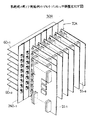
図2及び図3は本発明の第1実施例になるマルチプロセッサ装置50を示す。このマルチプロセッサ装置50は、クロスバーインターコネクト型のSMPである。また、このマルチプロセッサ装置50は、16枚のマザーボードユニット51−1〜51−16を有し、大量の情報を処理する能力を備えている。マルチプロセッサ装置50は、16枚のマザーボードユニット51−1〜51−16から選択された2枚のマザーボードユニット51の間の接続を切り換えることが可能となっている。サーバ90は、マルチプロセッサ装置50が、二点鎖線で示すシェルフ91内に収められた構成である。
【0036】
X1−X2は幅方向、Y1−Y2は奥行き方向、Z1−Z2は高さ方向である。
X−Y面が水平面、X−Z面及びY−Z面が垂直面である。また、同じ構成部品でも、区別するためには、添え字を付してある。区別しない場合には、添え字を付さない符号で示す。
【0037】
このマルチプロセッサ装置50は、8枚のクロスバーボードユニット60−1〜60−8と、第1のバックパネル70と、第2のバックパネル80と、16枚のマザーボードユニット51−1〜51−16とよりなる。
【0038】
8枚のクロスバーボードユニット60−1〜60−8は、長方形状であり、水平の姿勢で、Z1−Z2方向に等間隔で並んでいる。なお、バックパネル上のコネクタの配置によっては、クロスバーボードユニットは等間隔とならない場合もある。これは、他の実施例でも同じである。
【0039】
第1のバックパネル70は、垂直の姿勢とされて、クロスバーボードユニット60−1〜60−8の両側の長手方向の二つの辺61,62のうち一方の辺61にコネクタで接続してある。
【0040】
第2のバックパネル80は、垂直の姿勢とされて、クロスバーボードユニット60−1〜60−8の反対側の辺62にコネクタで接続してある。
【0041】
8枚のマザーボードユニット51−1〜51−8は、夫々が垂直の姿勢で、第1のバックパネル70に対して矢印Y1方向に挿入されてプラグインされてコネクタ接続されて、X1−X2方向に等間隔で並んでいる。
【0042】
残りの8枚のマザーボードユニット51−9〜51−16は、夫々が垂直の姿勢で、第2のバックパネル80に対して矢印Y2方向に挿入されてプラグインされてコネクタ接続されて、X1−X2方向に等間隔で並んでいる。
【0043】
マザーボードユニット51は、マザーボード52上に、CPU53とメモリモジュール54とが実装してあり、マザーボード51の挿入方向の先端の縁に沿って、複数のジャックコネクタ55が固定してある。
【0044】
第1のバックパネル70には、マザーボード51が接続される面71に、複数のプラグコネクタ72が実装してあり、クロスバーボードユニット60と接続される面73に、複数のプラグコネクタ74が実装してある。
【0045】
面71上の複数のプラグコネクタ72は、マザーボード51の接続のためのものであり、Z1−Z2方向に一列に並んで、且つ、この一列に並んだものがX1−X2方向に等間隔で8列を形成している。面73上の複数のプラグコネクタ74は、クロスバーボードユニット60との接続のためのものであり、X1−X2方向に一列に並んで、且つ、この一列に並んだものがZ1−Z2方向に等間隔で8行を形成している。
【0046】
図4に拡大して示すように、プラグコネクタ72のピン75aa〜75adは、第1のバックパネル70に設置されたスルーホール70a〜70dに半田付けもしくは圧入により電気的・機繊的に接続・保持されている。また、プラグコネクタ72の反対面に設置されたプラグコネクタ74のピン75ba〜75bdもバックパネル70に設置されたスルーホール70a〜70dに同様の方法で接続・保持されている。なお、本実施例ではプラグコネクタ実装方式として半田付けまたは圧入タイプで例示するが、このプラグコネクタ72及びプラグコネクタ74は表面実装タイプのものを使用しても良い。
【0047】
また、プラグコネクタ72と嵌合するマザーボードユニット51に設置されたジャックコネクタ55にはピン75aa〜75adに対応する接続ピン55a〜55dが設置してある。プラグコネクタ74と嵌合するクロスバーボードユニット60に設置されたジャックコネクタ84にはピン75ba〜75bdに対応する接続ピン84a〜84dが設置してある。
【0048】
プラグコネクタ72の各ピン75aa〜75adは等しい長さを持つが、ジャクコネクタのピン55a〜55dは等しい長さになっていない。プラグコネクタ74とジャックコネクタ84においても同様である。
【0049】
各ピンの長さの関係を以下に表す。説明の便宜上、以下の式では、ピンを表す符号をピン長さを表す符号として表現する。
【0050】
75aa=75ba=75ab=75bb=75ac=75bc=75ad=75bd
(55a=84a)>(55b=84b)>(55c=84c)>(55d=84d)
バックパネル70にはプラグコネクタ72とプラグコネクタ74とを接続する配線パターンa〜dが設置してある。配線aはジャックコネクタ55の最長ピン55aに接続するプラグピン75aaと、ジャックコネンクタ84の最短ピン84dと接続するプラグピン75bdを接続する配線パターンとなっている。続いて、配線bはジャックコネクタ55の2番目に長いピン55bに接続するプラグピン75abと、ジャックコネクタ84の2番目に短いピン75bcを接続する配線パターンである。以下同様にジャックコネクタ55〜84までの接続経路をピンの符号を用いて表すと、配線パターンcの接続経路は、ピン55c→ピン75ac→配線パターンc→ピン75bc→ピン84bとなっている。配線パターンdの接続経路は、ピン55d→ピン75ad→配線パターンd→ピン75ba→ピン84aとなっている。
【0051】
ここで、ジャックコネクタ55と84のピンの長さに以下の関係
(55a+84d)=(55b+84c)=(55c=84b)=(55d=84a)=同一長さ。
が成り立場合に、バックパネル上の配線パターンa〜dを等しい長さで配線すれば、ジャックコネクタ55のマザーボードユニット上の接続点55aa〜55adと、ジャックコネクタ84のクロスバーボードユニット上の接続点84aa〜84adの接続距離を全て等長で接続できる。この方式と後述の図3及び図7で説明するクロスバーボード上の、等長配線を組み合わせることで、マザーボードユニットからクロスバーボードユニット上のスイッチング素子63(または101、102)までを等長に接続できる。
【0052】
更に、マザーボード内でCPU素子・MEM素子との接続線長を考慮することにより、マザーボード上のCPU〜バックパネル〜クロスバーボード〜クロスバーボード上のスイッチング素子までの接続を等長にでき、信号伝送時間を同じにできる。これにより理想的なSMPが実現できる。
【0053】
更に、先に述べたジャックコネクタにおいて前述の式が成立しない場合においても、バックパネル内の配線a〜dの長さを調整し、マザーボードユニットからクロスバーボードユニットまでの接続長さを等しくすることにより、同様の効果がある。
【0054】
例えば、以下、ジャックコネクタの各ピンの長さを仮に下記の値に置き換えて説明する。
【0055】
55a=84a=5mm、55b=84b=4mm、55c=84c=3.5mm、55d=84d=3mm。
(55a+84d)=8mm、(55b+84c)=7.5mm。
(55c+84b)=7.5mm、(55d+84a)=8mm。
前述の(55a+84d)〜(55d+・84a)まで全てが同一長さの式が成立しない。
【0056】
しかし、バックパネル上の配線長さを以下の関係にすることにより等長配線が可能である。
(配線a長さ)=(配線b長さ)+((55a+84d)−(55b+84c))
(配線d長さ)=(配線c長さ)+((55d+84a)一(55c+84b))
つまり,ジャックコネクタのピン長さの違いをバックパネルや配線の長さを調整することで、すべての接続経路が等長になることを意味する。
【0057】
この方法は、図4に例示した通りの、対応するピン間を接続しない場合でも有効である。
【0058】
方法としては、先ずバックパネル上で接続する必要のあるピン間を、接続し得る最短で全て配線する。次に、接続したすべての配線長さとジャックコネクタのピン長さを含めた接続の長さを算出する。この算出された接続長さのうち一番長い接続長さを基準とし、それ以外のもの接続長さと先の基準とした接続長さとの差を各々求め、その差の長さを各々のバックパネル上の配線の長さに加えれば良い。
【0059】
また、プラグコネクタ、ジャックコネクタとして図5に示すものを用いても良い。
【0060】
図5に拡大して示すように、プラグコネクタ72は、第1のバックパネル70を貫通している長いピン端子75の一端側75aがシュラウド76内に突き出ている構成であり、プラグコネクタ74は、この長いピン端子75の反対側75bがシュラウド77内に突き出ている構成である。
【0061】
また、図5に示すように、第1のバックパネル70の面71には、スイッチング機能を有する電子部品78a、受動・駆動機能を有する電子部品78b、メモリ又はバッファ機能を有する電子部品78c、抵抗部品78d、コンデンサ部品78eが実装してある。
【0062】
この場合、図5の接続においてはバックパネル上の配線が存在しない。
従って等長配線を行うためには、マザーボードユニット上のジャックコネクタのボード実装部からクロスバーボードユニット上のジャックコネクタのボード実装部までの接続距離を求め,その一番長い接続長さを基準とし、クロスバーボードユニット上の配線により先の基準とする接続長さとそれ以外の各々の接続長との差をクロスバーボード上の配線長さで調整することにより、接続経路の等長化が実現できる。
【0063】
第2のバックパネル80は、上記の第1のバックパネル70と同じ構成である。マザーボード51が接続される面81上の複数のプラグコネクタ82は、Z1−Z2方向に一列に並んで、且つ、この一列に並んだものがX1−X2方向に等間隔で8列を形成している。クロスバーボードユニット60と接続される面83上の複数のプラグコネクタ84は、X1−X2方向に一列に並んで、且つ、この一列に並んだものがZ1−Z2方向に等間隔で8行を形成している。プラグコネクタ82、84は、夫々、上記のプラグコネクタ82、84と同じ構成である。
【0064】
図3に示すように、クロスバーボードユニット60は、ボード61の上面の中央に一つのスイッチング素子63が実装してあり、一つの長手方向の辺62aに沿って、8つのジャックコネクタ64が、上記の第1のバックパネル70上のプラグコネクタ74に対応した配置で実装してあり、別の長手方向の辺62bに沿って、8つのジャックコネクタ65が、上記の第2のバックパネル80上のプラグコネクタ84に対応した配置で実装してある。また、ボード61には、個々のジャックコネクタ64とスイッチング素子63の対応する端子との間を接続する配線パターン66が複数本形成してあり、且つ、個々のジャックコネクタ65とスイッチング素子63の対応する端子との間を接続する配線パターン67が複数本形成してある。配線パターン66及び配線パターン67は適宜屈曲してあり、個々の配線パターン66の長さ及び個々の配線パターン67の長さは等しい。即ち、クロスバーボードユニット60は、スイッチング素子63と各ジャックコネクタ64、65との間の配線パターン66、67の長さが全て等しい、所謂、等長配線の構造となっている。
【0065】
クロスバーボードユニット60の8つのジャックコネクタ64には、第1のバックパネル70のピンコネクタ74が接続してある。クロスバーボードユニット60の別の8つのジャックコネクタ65には、第2のバックパネル80のピンコネクタ84が接続してある。よって、第1のバックパネル70と第2のバックパネル80とは、クロスバーボードユニット60を両側から挟む位置関係にある。
【0066】
ここで、ジャックコネクタ55―プラグコネクタ72―プラグコネクタ74−ジャックコネクタ64の部分を第1のコネクタ接続部分95という。ジャックコネクタ55―プラグコネクタ82―プラグコネクタ84−ジャックコネクタ65の部分を第2のコネクタ接続部分96という。
【0067】
上記構成になるマルチプロセッサ装置50において、マザーボードユニット51−1〜51−16のうちの任意の異なる二つのマザーボードユニットを接続する態様は、以下の三つに大別される。なお、二つのマザーボードユニットの間の接続とは、説明の便宜上一のマザーボードユニットのCPU53と別のマザーボードユニットのメモリモジュール54との間の接続を意味する。更に説明の便宜上、接続の対象は、二つのマザーボードユニットとして説明する。
(1)第1のバックパネル70にプラグイン接続してあるマザーボードユニット51−1〜51−8のうちの任意の異なる二つのマザーボードユニットの間の接続
例えば、マザーボードユニット51−1とマザーボードユニット51−7との間は、第1のコネクタ接続部分95−1―配線パターン66−1−スイッチング素子63―配線パターン66−7−第1のコネクタ接続部分95−7を経て接続される。
(2)第2のバックパネル80にプラグイン接続してあるマザーボードユニット51−9〜51−16のうちの任意の異なる二つのマザーボードユニットの間の接続
例えば、マザーボードユニット51−11とマザーボードユニット51−14との間は、第2のコネクタ接続部分95−3―配線パターン67−3−スイッチング素子63―配線パターン66−6−第2のコネクタ接続部分95−6を経て接続される。
(3)第1のバックパネル70にプラグイン接続してあるマザーボードユニット51−1〜51−8のうちの任意の一つのマザーボードユニットと第2のバックパネル80にプラグイン接続してあるマザーボードユニット51−9〜51−16のうちの任意の一つのマザーボードユニットの間の接続
例えば、マザーボードユニット51−1とマザーボードユニット51−11との間は、第1のコネクタ接続部分95−1―配線パターン66−1−スイッチング素子63―配線パターン67−3−第2のコネクタ接続部分96−3を経て接続される。
【0068】
なお、同じマザーボードユニット51内におけるCPU53のメモリモジュール54への信号の伝送は、クロスバーボードユニット60のスイッチング素子63を通って、スイッチング素子63で折り返される経路を経てなされ、信号の伝送距離は、上記(1)、(2)、(3)の接続態様の場合と同じである。よって、同じマザーボードユニット51におけるCPU53のメモリモジュール54に対するアクセス速度は、上記(1)、(2)、(3)の接続態様の場合と同じである。
【0069】
上記のマルチプロセッサ装置50は、以下の特長を有する。
【0070】
1 従来に比べて情報の処理を高速で行うことが可能である。
【0071】
上記(1)、(2)、(3)の接続態様において、接続の経路の長さが長くなり易いのは、(3)の接続態様である。この(3)の接続態様における接続の経路の長さは、図1に示す従来例に比べて、ケーブル30の長さ分短くなっている。
【0072】
よって、信号の伝送距離は短くなり、これによって、信号の伝送ひずみが発生しにくくなり、よって、信号の転送レートを低く抑えなければならないという従来の制限が緩和され、従来に比べて信号の転送レートを上げることが出来、よって、従来に比べて情報の処理を高速で行うことが出来る。
【0073】
2 SMPが理想的に実現できる。
【0074】
接続の経路の長さは、上記(1)、(2)、(3)の接続態様において等しいので、接続態様がどのように変更されても、信号の伝送距離は変化せずに同じであり、各CPU53の各メモリモジュール54に対するアクセス速度は等しい。よって、SMPが理想的に実現できる。
【0075】
3 従来に比べて小型に構成することが可能である。
【0076】
従来のマルチプロセッサ装置10において使用されているケーブル30が使用されていないため、マルチプロセッサ装置50は小型に構成出来る。
【0077】
マルチプロセッサ装置50が小型であるため、サーバ90も高さが例えば1800mm、幅が例えば1000mm、奥行きが例えば1000mmと、小型に構成出来る。
【0078】
4 従来に比べて信頼性を向上することが可能である。
【0079】
ケーブルの接続がなく、ケーブルの接続不良に伴う故障が起きないからである。
【0080】
なお、図2中、88はクロスバーボードユニット・バックパネル組立体であり、8枚のクロスバーボードユニット60−1〜60−8と、第1のバックパネル70と、第2のバックパネル80とよりなる構造である。
【0081】
図6は、上記のマルチプロセッサ装置50を構成するクロスバーボードユニット60の変形例であるクロスバーボードユニット60Aを、第1のバックパネル70及び第2のバックパネル80と併せて示す。
【0082】
クロスバーボードユニット60Aは、ボード61Aの上面のX2側寄りの部位に第1スイッチング素子101が実装してあり、X1側寄りの部位に第2スイッチング素子102が実装してある。ジャックコネクタ64A、65Aは、図3のジャックコネクタ64、65と対応した配置で設けてある。ボード61Aには、個々のジャックコネクタ64Aと第1スイッチング素子101の対応する端子との間を接続する複数の配線パターン103と、個々のジャックコネクタ65Aと第2スイッチング素子102の対応する端子との間を接続する複数の配線パターン104と、第1スイッチング素子101と第2スイッチング素子102との間を接続する複数の配線パターン105とが形成してある。個々の配線パターン103は適宜屈曲してあり、個々の配線パターン103の長さは等しい。同じく、個々の配線パターン104は適宜屈曲してあり、個々の配線パターン104の長さは等しい。個々の配線パターン105の長さは等しい。ここで、個々の配線パターン103の長さと個々の配線パターン104の長さとは等しい。クロスバーボードユニット60Aも、所謂、等長配線の構成となっている。
【0083】
マザーボードユニット51−1〜51−16のうちの任意の異なる二つのマザーボードユニットは、接続の経路の長さが変わらない状態で、接続される。
【0084】
〔第2実施例〕
図7は本発明の第2実施例になるマルチプロセッサ装置50Bを示す。このマルチプロセッサ装置50Bは、クロスバーインターコネクト型のSMPであり、図2に示すマルチプロセッサ装置50のマザーボードユニット51の数より更に8枚多い、合計24枚のマザーボードユニットを有する構成である。
【0085】
このマルチプロセッサ装置50Bは、図2に示すマルチプロセッサ装置50を基本とし、このY2方向側に、マザーボードユニット51−17〜51−24等が増設された構造である。増設されたボードユニット及びパネルには、「拡張」を付す。
【0086】
マルチプロセッサ装置50Bは、図2に示すマルチプロセッサ装置50と、マザーボードユニット51−1〜51−8のY2方向端にコネクタ接続されている第1の拡張バックパネル110と、第1の拡張バックパネル110のY2方向の面にコネクタ接続されて、水平の姿勢で、Z1−Z2方向に等間隔で並んでいる8枚の拡張クロスバーボードユニット120−1〜120−8と、拡張クロスバーボードユニット120−1〜120−8のY2方向端にコネクタ接続されている第2の拡張バックパネル130と、第2の拡張バックパネル130のY2方向の面にコネクタ接続されて、垂直の姿勢で、X1−X2方向に等間隔で並んでいる8枚の拡張マザーボードユニット51−17〜51−24とよりなる構造である。
【0087】
同様にして、Y1−Y2方向に更に拡張して、マザーボードユニット51を更に増設した構成とすることも可能である。
【0088】
このマルチプロセッサ装置50Bは、前記のマルチプロセッサ装置50と同様の効果を有する。
【0089】
〔第3実施例〕
図8は本発明の第3実施例になるマルチプロセッサ装置50Cを示す。このマルチプロセッサ装置50Cは、クロスバーインターコネクト型のSMPであり、図2に示すマルチプロセッサ装置50のマザーボードユニット51の数より更に16枚多い、合計32枚のマザーボードユニットを有する構成である。
【0090】
このマルチプロセッサ装置50Cは、大略、図2に示すマルチプロセッサ装置50の上側に同じマルチプロセッサ装置50を積み重ねた構造である。換言すれば、図2に示すマルチプロセッサ装置50のZ1方向側に、マザーボードユニット51−17〜51−32等が増設された構造である。増設されたボードユニット及びパネルには、「拡張」を付す。
【0091】
マルチプロセッサ装置50Cは、図2に示すマルチプロセッサ装置50と、第1のバックパネル70のZ1方向の端にコネクタ170によって接続されて、Z1方向に張り出している第1の拡張バックパネル140と、第2のバックパネル80のZ1方向の端にコネクタ180によって接続されて、Z1方向に張り出している第2の拡張バックパネル150と、第1の拡張バックパネル140と第2の拡張バックパネル150との対向する面にコネクタ接続されて、水平の姿勢で、Z1−Z2方向に等間隔で並んでいる8枚の拡張クロスバーボードユニット180−1〜180−8と、第1の拡張バックパネル140のY2方向の面にコネクタ接続されて、垂直の姿勢で、X1−X2方向に等間隔で並んでいる8枚の拡張マザーボードユニット51−17〜51−24と、第2の拡張バックパネル150のY2方向の面にコネクタ接続されて、垂直の姿勢で、X1−X2方向に等間隔で並んでいる8枚の拡張マザーボードユニット51−25〜51−32とよりなる構造である。
【0092】
同様にして、Z1−Z2方向に更に拡張して、マザーボードユニット51を更に増設した構成とすることも可能である。
【0093】
このマルチプロセッサ装置50Cは、前記のマルチプロセッサ装置50と同様の効果を有する。
【0094】
〔第4実施例〕
図9 は本発明の第4実施例になるマルチプロセッサ装置50Dを示す。このマルチプロセッサ装置50Dは、クロスバーインターコネクト型のSMPであり、図2に示すマルチプロセッサ装置50のマザーボードユニット51の数より更に8枚多い、合計24枚のマザーボードユニットを有する構成であり、柱状である構造に特徴がある。
【0095】
このマルチプロセッサ装置50Dは、8枚のクロスバーボードユニット190−1〜190−8と、第1のバックパネル70と、第2のバックパネル80と、第3のバックパネル180と、16枚のマザーボードユニット51−1〜51−24とよりなる。
【0096】
各クロスバーボードユニット190−1〜190−8は、正三角形であり、三つの辺に沿って複数のコネクタ191が実装してあり、且つ、上面にスイッチング素子192、193が実装してあり、水平の姿勢で、Z1−Z2方向に等間隔で並んでいる。
【0097】
第1のバックパネル70、第2のバックパネル80、第3のバックパネル180は、垂直の姿勢とされて、クロスバーボードユニット190−1〜190−8の三つの辺にコネクタで接続してあり、正三角柱状をなしている。
【0098】
第1のバックパネル70にはマザーボードユニット51−1〜51−8が、第2のバックパネル80にはマザーボードユニット51−9〜51−16が、第3のバックパネル200にはマザーボードユニット51−17〜51−24が、コネクタ接続されて、垂直の姿勢で、各バックパネルの幅方向に等間隔で並んでいる。
【0099】
このマルチプロセッサ装置50Dは、前記のマルチプロセッサ装置50と同様の効果を有する。
【0100】
クロスバーボードユニットとして、正方形、正五角形、正六角形等、又は、正のつかない三角形、四角形、五角形、六角形等を使用してもよい。マルチプロセッサ装置は、クロスバーボードユニットの形状に対応した柱形状となる。
【0101】
〔第5実施例〕
図10及び図11は本発明の第5実施例になるマルチプロセッサ装置50Eを示す。このマルチプロセッサ装置50Eは、クロスバーインターコネクト型のSMPであり、図2に示すマルチプロセッサ装置50とは、クロスバーボードユニットのバックパネルに対するコネクタ接続の方向を異にする。
【0102】
このマルチプロセッサ装置50Eは、8枚のクロスバーボードユニット60E−1〜60E−8と、第1のバックパネル70Eと、第2のバックパネル80Eと、16枚のマザーボードユニット51−1〜51−16とよりなる。
【0103】
クロスバーボードユニット60E−1〜60E−8は、ボード61の上面61aの中央に一つのスイッチング素子63が実装してあり、図11に拡大して示すように、下面61bのうち長手方向の辺に沿う場所に、ジャックコネクタ200、201が、接続口側がZ2方向を向く姿勢で実装してある。
【0104】
第1のバックパネル70Eの面73Eには、プラグコネクタ202がそのピンがZ2方向を向く姿勢で実装してある。第2のバックパネル80Eの面83Eには、プラグコネクタ203がそのピンがZ2方向を向く姿勢で実装してある。
【0105】
8枚のクロスバーボードユニット60E−1〜60E−8は、水平の姿勢で、Z1−Z2方向に等間隔で並んでいる。
【0106】
第1のバックパネル70E及び第2のバックパネル80Eは、垂直の姿勢とされて対向している。クロスバーボードユニット60E−1〜60E−8上のジャックコネクタ200、201が夫々第1のバックパネル70E上のプラグコネクタ202及び第2のバックパネル80E上のプラグコネクタ203と接続してある。マザーボードユニット51−1〜51−8、51−9〜51−16は、夫々が垂直の姿勢で、第1のバックパネル70E及び第2のバックパネル80Eにコネクタ接続されて、X1−X2方向に等間隔で並んでいる。
【0107】
ジャックコネクタ200、201のプラグコネクタ202、203への接続は、クロスバーボードユニット60E−1〜60E−8を矢印C2で示すように、Z2の方向に押し下げることによってなされている。また、ジャックコネクタ200、201のプラグコネクタ202、203からの接続の解除は、クロスバーボードユニット60E−1〜60E−8を矢印C1で示すように、Z1の方向に押し上げることによってなされる。
【0108】
例えばクロスバーボードユニット60E−5は、最初に、図11に示すように、矢印C1で示すようにZ1の方向に押し上げて、ジャックコネクタ200、201をプラグコネクタ202、203から抜き、次いで、図10に示すように、矢印D2で示すようにX2の方向に引き抜くことによって、マルチプロセッサ装置50Eより取り外される。新たなクロスバーボードユニット60Eは、上記の取り外しとは逆の操作、即ち、マルチプロセッサ装置50Eの側面側より矢印D2で示すように挿入し、次いで、矢印C2で示すように押し下げることによって、取り付けられる。
【0109】
よって、クロスバーボードユニット60E−1〜60E−8のうちの一つのクロスバーボードユニットが故障した場合には、マルチプロセッサ装置50Eを分解せずに、即ち、対向している第1のバックパネル70E及び第2のバックパネル80Eを移動させたり、取り外したりせずに、垂直の姿勢とされて対向している。故障したクロスバーボードユニットを新しいクロスバーボードユニットと交換することが可能となる。よって、マルチプロセッサ装置50Eは、保守作業を少ない工数で行うことが可能であり、良好な保守性を有する。
【0110】
〔第6実施例〕
図12は本発明の第6実施例になるマルチプロセッサ装置50Fを示す。このマルチプロセッサ装置50Fは、クロスバーインターコネクト型のSMPであり、図2に示すマルチプロセッサ装置50に、放熱部品210が追加されている構造である。
【0111】
放熱部品210は、アルミニウム製であり、断面が長方形である中空部211を有する中空状の部品であり、各クロスバーボードユニット60−1〜60−8毎に、その上面に、水平の姿勢で、スイッチング素子63の上面に接触して設けてある。各放熱部品210は、隣り合うクロスバーボードユニット60の間の空間内に収まっている。中空部211の大きさは、冷却風の風量と風速の関係により、最適に定めてある。
【0112】
マルチプロセッサ装置50Fが組み込まれたサーバ内には、冷却ファンが設けてあり、冷却風が符号212で示すようにX1方向に流れる。よって、冷却風は、放熱部品210の外周の面及び内周の面に接触して流れる。よって、各クロスバーボードユニット60−1〜60−8上のスイッチング素子63で発生した熱が効率良く奪われ、スイッチング素子63が効率良く強制空冷される。
【0113】
〔第7実施例〕
図13は本発明の第7実施例になるマルチプロセッサ装置50Gを示す。このマルチプロセッサ装置50Gは、クロスバーインターコネクト型のSMPであり、図2に示すマルチプロセッサ装置50に、電源の供給を行う第1の電源ユニット221及び第2の電源ユニット222を追加して設けてある構成である。第1の電源ユニット221と第2の電源ユニット222とは夫々独立しており、第1の電源ユニット221は第1のバックパネル70と接続してあり、第2の電源ユニット222は第1のバックパネル70と接続してある。第1の電源ユニット221と第2の電源ユニット222とは並列に接続されている。また、第1の電源ユニット221及び第2の電源ユニット222は、一台でも、マルチプロセッサ装置50G全体を消費電力をまかなうことが可能である容量を有する。
【0114】
第1のバックパネル70、8枚のマザーボードユニット51−1〜51−8、クロスバーボードユニット60−1〜60−8は、第1の電源ユニット221から電源を供給されている。第2のバックパネル80、8枚のマザーボードユニット51−9〜51−16は、第2の電源ユニット222から電源を供給されている。ここで、第1の電源ユニット221が故障した場合には、第1のバックパネル70、8枚のマザーボードユニット51−1〜51−8、クロスバーボードユニット60−1〜60−8は、第2の電源ユニット222から電源を供給され、マルチプロセッサ装置50Gは正常に動作し続ける。第2の電源ユニット222が故障した場合には、第2のバックパネル80、8枚のマザーボードユニット51−9〜51−16は、第1の電源ユニット221のみから電源を供給され、マルチプロセッサ装置50Gは正常に動作し続ける。
【0115】
〔第8実施例〕
図14は本発明の第8実施例になるマルチプロセッサ装置50Hを示す。このマルチプロセッサ装置50Hは、クロスバーインターコネクト型のSMPであり、図2に示すマルチプロセッサ装置50と実質的に同じ構造であり、X1−X2方向の寸法の大きさが図2に示すマルチプロセッサ装置50より大きい。
【0116】
第1のバックパネル70H及び第2のバックパネル80Hは、X1−X2方向の寸法が図2中のバックパネル70、80より長い。第1のバックパネル70Hには、12枚のマザーボードユニット51−1〜51−12が垂直の姿勢でコネクタ接続されて、X1−X2方向に等間隔で並んでいる。第2のバックパネル80Hには、12枚のマザーボードユニット51−13〜51−24が垂直の姿勢でコネクタ接続されて、X1−X2方向に等間隔で並んでいる。
【0117】
8枚のクロスバーボードユニット組立体230−1〜230−8は、長方形状であり、水平の姿勢で、Z1−Z2方向に等間隔で並んでいる。第1のバックパネル70H及び第2のバックパネル80Hは、8枚のクロスバーボードユニット組立体230−1〜230−8の両側からコネクタ接続してあり、対向している。
【0118】
クロスバーボードユニット組立体230−1は、図2中のクロスバーボードユニット60−1の長手方向の両側に、拡張クロスバーボード231,232を接続して設けた構成である。クロスバーボードユニット60−1のボード61は、拡張クロスバーボード231,232を考慮した配線パターンを有し、拡張クロスバーボード231,232は、ボード61と似た配線パターンを有する。
【0119】
図15に併せて示すように、拡張クロスバーボード231とクロスバーボードユニット60−1とは、電気的には、平行ボード接続コネクタ装置(スタッキングコネクタ装置)240によって接続してあり、機械的には、上下面より板状の補強金具250、251で挟んで、ねじ252、253でねじ止めされて接続してある。図14は、補強金具250を取り外した状態で示す。
【0120】
スタッキングコネクタ装置240は、フラットケーブル部241と、このフラットケーブル部241の両端側の下面に取り付けてあるスタッキング雄コネクタ242,243と、拡張クロスバーボード231の端の上面に固定してあるスタッキング雌コネクタ244と、ボード61の端の上面に固定してあるスタッキング雌コネクタ245とよりなる。スタッキング雄コネクタ242,243が夫々スタッキング雌コネクタ244、245に接続されている。
【0121】
拡張クロスバーボード232とクロスバーボードユニット60−1との接続も、上記と同じく、スタッキングコネクタ装置240及び補強金具250aによってなされている。
【0122】
即ち、クロスバーボードユニット組立体230−1は、クロスバーボードユニット60−1が長手方向に、拡張された構造となっている。他のクロスバーボードユニット組立体230−2〜230−8も、上記のクロスバーボードユニット組立体230−1と同じ構造である。よって、既存のリフロー炉を使用して、X1−X2方向の寸法が通常より長いバックパネル70H、80Hに対応したクロスバーボードユニット組立体230を製造することが可能である。
【0123】
〔第9実施例〕
図16は本発明の第9実施例になるマルチプロセッサ装置50Iを示す。マルチプロセッサ装置50Iは、図14に示すマルチプロセッサ装置50Hとは、各クロスバーボードユニット60−1〜60−8の長手方向の片側に配されている拡張クロスバーボード255が、各クロスバーボードユニット60−1〜60−8と同じくバックパネル70I、80Iとコネクタ接続されており、且つ、フレキシブル基板の両端にコネクタを有するフレキシブルケーブルコネクタ装置256によって、拡張クロスバーボード255の端部とバックパネル80Iとコネクタ接続されている構成が相違する。
【0124】
フレキシブルケーブルコネクタ装置256を利用することによって、拡張クロスバーボード255のバックパネル80Iとの接続の箇所が通常より一つ多くなっている。
【0125】
〔第10実施例〕
図17は本発明の第10実施例になるマルチプロセッサ装置50Jを示す。このマルチプロセッサ装置50Jは、クロスバーインターコネクト型のSMPであり、図2に示すマルチプロセッサ装置50とは、マザーボードユニット及びバックパネルが相違する構成である。
【0126】
このマルチプロセッサ装置50Jは、8枚のクロスバーボードユニット60−1〜60−8と、16枚のマザーボードユニット51J−1〜51J−16とよりなる。
【0127】
マザーボードユニット51Jは、図2中の一つのマザーボードユニット51に、短冊状のパネル260又は261が接続してある構成である。短冊状のパネル260、261は、図2中の一つのマザーボードユニット51に対応する幅Wを有する。例えば、マザーボードユニット51J−8は、図2中の一つのマザーボードユニット51のY1方向の端に短冊状のパネル260−8が接続されている構成である。マザーボードユニット51J−9は、図2中の一つのマザーボードユニット51のY2方向の端に短冊状のパネル261−9が接続されている構成である。
【0128】
8枚のマザーボードユニット51J−1〜51J−8は、夫々が垂直の姿勢で、クロスバーボードユニット60−1〜60−8に対して矢印Y1方向に挿入されてプラグインされてコネクタ接続されて、X1−X2方向に等間隔で並んでいる。残りの8枚のマザーボードユニット51J−9〜51J−16は、夫々が垂直の姿勢で、クロスバーボードユニット60−1〜60−8に対して矢印Y2方向に挿入されてプラグインされてコネクタ接続されて、X1−X2方向に等間隔で並んでいる。
【0129】
並んでいる短冊状のパネル260−1〜260−8が、第1のバックパネル70Jを形成している。並んでいる短冊状のパネル261−9〜261−16が、第2のバックパネル80Jを形成している。
【0130】
このマルチプロセッサ装置50Jは、バックパネル70J、80Jがマザーボードユニットの単位で短冊状に分割されている構成であり、大型化が容易である。
【0131】
また、バックパネルが一枚の構成である場合は、工場内でのマルチプロセッサ装置の組立ては、図18に示すように、バックパネル265をその周囲をラックのフレーム266に固定し、クロスバーボードユニット60−1〜60−8を一つずつ矢印E1で示すよう押して、バックパネル265の面にコネクタ接続させて行う。ここで、一つのクロスバーボードユニット60にコネクタが複数あり、全部のコネクタを同時に接続させるために、クロスバーボードユニット60−1〜60−8を強く押す必要がある。このため、この組立て工程において、バックパネル265が、二点鎖線で示すように反ってしまう場合がある。よって、場合によっては、この後に、マザーボードユニット51を矢印E2で示すようにプラグイン接続した場合に、マザーボードユニット51のバックパネル265に対する接続が不完全となる虞れがあった。
【0132】
しかし、本実施例のようにバックパネル70J、80Jがマザーボードユニットの単位で短冊状に分割されている構成である場合には、先ず、8枚のクロスバーボードユニット60−1〜60−8をラックのフレーム(図示せず)に固定し、この固定してある8枚のクロスバーボードユニット60−1〜60−8に対して短冊状のパネル付きのマザーボードユニット51Jをプラグイン接続するため、短冊状のパネルが反ることは起きない。よって、マザーボードユニット51Jの8枚のクロスバーボードユニット60−1〜60−8に対するコネクタ接続は良好になされる。
【0133】
〔第11実施例〕
図19は本発明の第11実施例になるマルチプロセッサ装置50Kを示す。このマルチプロセッサ装置50Kは、クロスバーインターコネクト型のSMPであり、図17に示すマルチプロセッサ装置50Kと略同じ構造であり、図2に示すマルチプロセッサ装置50とはバックパネルの構造が相違する構造である。
【0134】
このマルチプロセッサ装置50Kは、8枚のクロスバーボードユニット60−1〜60−8と、第1のバックパネル70Kと、第2のバックパネル80Kと、16枚のマザーボードユニット51−1〜51−16とよりなる。
【0135】
第1のバックパネル70Kは、図17に示す短冊状のパネル260−1〜260−8よりなり、各短冊状のパネル260−1〜260−8が独立にクロスバーボードユニット60−1〜60−8にコネクタ接続されて、X1−X2方向に並んだ構造である。同じく、第2のバックパネル80Kは、図16に示す短冊状のパネル261−9〜261−16よりなり、各短冊状のパネル261−9〜261−16が独立にクロスバーボードユニット60−1〜60−8にコネクタ接続されて、X1−X2方向に並んだ構造である。
【0136】
このマルチプロセッサ装置50Kは、バックパネル70K、80Kがマザーボードユニット51の単位で短冊状に分割されている構成であり、大型化が容易である。
【0137】
また、このマルチプロセッサ装置50Kの組立ては、先ず、8枚のクロスバーボードユニット60−1〜60−8をラックのフレーム(図示せず)に固定し、この固定してある8枚のクロスバーボードユニット60−1〜60−8に対して短冊状のパネル260−1〜260−8、261−9〜261−16を1枚ずつコネクタ接続する。よって、完成した第1のバックパネル70K及び第2のバックパネル80Kは、反りの無い状態となる。よって、マザーボードユニット51の第1のバックパネル70K及び第2のバックパネル80Kに対するコネクタ接続は良好になされる。
【0138】
〔第12実施例〕
図20は本発明の第12実施例になるマルチプロセッサ装置50Lを示す。このマルチプロセッサ装置50Lは、クロスバーインターコネクト型のSMPであり、図2に示すマルチプロセッサ装置50とはバックパネルの構造が相違する構造である。
【0139】
このマルチプロセッサ装置50Lは、8枚のクロスバーボードユニット60−1〜60−8と、第1のバックパネル70Lと、第2のバックパネル80Lと、16枚のマザーボードユニット51−1〜51−16とよりなる。
【0140】
第1のバックパネル70Lは、一つのクロスバーボードユニット60に対応するX1−X2方向に長い短冊状のパネル270−1〜270−8が独立にクロスバーボードユニット60−1〜60−8にコネクタ接続されて、Z1−Z2方向に並んだ構造である。第2のバックパネル80Lは、一つのクロスバーボードユニット60に対応するX1−X2方向に長い短冊状のパネル280−1〜280−8が独立にクロスバーボードユニット60−1〜60−8にコネクタ接続されて、Z1−Z2方向に並んだ構造である。
【0141】
各マザーボードユニット51−1〜51−8は、短冊状のパネル270−1〜270−8を跨いでいる。各マザーボードユニット51−9〜51−16は、短冊状のパネル280−1〜280−8を跨いでいる。
【0142】
このマルチプロセッサ装置50Lは、バックパネル70L、80Lがクロスバーボードユニット60の単位で短冊状に分割されている構成であり、大型化が容易である。
【0143】
クロスバーボードユニット60−1〜60−8と、第1のバックパネル70Lと、第2のバックパネル80Lとが、マルチプロセッサ装置50Lの芯の部分を形成するクロスバーボードユニット・バックパネル組立体300を構成する。
【0144】
また、電圧V1を出力する電源ユニット290と、電圧V2を出力する電源ユニット291とが設けてある。電源ユニット290は、偶数番の短冊状のパネル270−2、270−4、270−6、270−8、280−2、280−4、280−6、280−8に接続してある。電源ユニット291は、奇数番の短冊状のパネル270−1、270−3、270−5、270−7、280−1、280−3、280−5、280−7に接続してある。また、各マザーボードユニット51−1〜51−16は、電源層を二つ有する構成である。
【0145】
各マザーボードユニット51−1〜51−16には、その一の電源層には電圧V1が加えられ、別の電源層には電圧V2が加えられる。即ち、各マザーボードユニット51−1〜51−16には、異なる二つの電圧が加えられる。よって、各マザーボードユニット51−1〜51−16には、動作電圧がV1である半導体素子と動作電圧がV2である半導体素子とが混在して実装される。
【0146】
次に、上記のクロスバーボードユニット・バックパネル組立体300の変形例について説明する。
【0147】
図21は、第1の変形例になるクロスバーボードユニット・バックパネル組立体300Aを示す。このクロスバーボードユニット・バックパネル組立体300Aは、クロスバーボード・短冊状パネル組立体301−8〜301−1が、そのクロスバーボード60の四隅の孔302を四方に配されたガイドポール303−1〜303−4に嵌合させて積み重ねられており、ガイドポール303−1〜303−4によって積み重ねられた状態に固定されている構造である。
【0148】
クロスバーボード・短冊状パネル組立体301−1は、クロスバーボードユニット60−1と、これを両側に挟むようにコネクタ接続してある短冊状のパネル270−1及び280−1とよりなる構造である。他のクロスバーボード・パネル組立体301−2〜301−8も同様の構成である。
【0149】
また、ガイドポール303−1〜303−4はアルミニウム製であり、電源ユニット304がガイドポール303−1〜303−4に接続してある。クロスバーボード60には、孔302に臨む部位に端子部材305が設けてあり、積み重ねられた状態では、端子部材305がガイドポール303−1〜303−4と接触してある。よって、電源ユニット304からの電圧が、全部のクロスバーボードユニット60−1〜60−8にガイドポール303−1〜303−4を介して効率的に加えられ、更には、バックパネル70L、80Lに効率的に加えられる。このため、この構成は、クロスバーボードユニット60−1〜60−8への供給電力が大きいものである場合、及び、バックパネル70L、80Lへの供給電力が大きいものである場合に適用して有効である。即ち、クロスバーボードユニット60−1〜60−8上での電圧降下、及びバックパネル70L、80L上での電圧降下を抑制することが可能である。
【0150】
図22は、第2の変形例になるクロスバーボードユニット・バックパネル組立体300Bを示す。複数のガイドレール310が、クロスバーボード・短冊状パネル組立体301に対応した配置で固定してある。クロスバーボード・短冊状パネル組立体301−1〜301−8は、その両側の短冊状のパネル270−1〜270−8及び280−1〜280−8の上下の縁を、ガイドレール310に嵌合されて支持されて、積み重ねられた状態に配置されている構造である。
【0151】
短冊状のパネル270−1〜270−8は、平面状に並んで、第1のバックパネル70Lを形成する。短冊状のパネル280−1〜280−8は、平面状に並んで、第2のバックパネル80Lを形成する。
【0152】
各ガイドレール310には、ばね性を有する電源供給端子311が組み込まれており、電源ユニット312が電源供給端子311に接続されている。よって、電源ユニット312からの電圧が、ガイドレール310内の電源供給端子311を通して全部の短冊状のパネル270−1〜270−8及び280−1〜280−8に加えられており、バックパネル70L、80L上での電圧降下の発生が抑制できるようになっている。
【0153】
また、矢印G2方向に引くことによって、クロスバーボード・短冊状パネル組立体301−1〜301−8のうち任意のクロスバーボード・短冊状パネル組立体301だけを引き出すことが可能である。よって、故障した場合に、故障したクロスバーボード・短冊状パネル組立体の交換を容易に行うことが可能であり、クロスバーボードユニット・バックパネル組立体300Bは保守が容易である。
【0154】
〔第13実施例〕
図23は本発明の第13実施例になるマルチプロセッサ装置50Mを示す。このマルチプロセッサ装置50Mは、クロスバーインターコネクト型のSMPであり、図2に示すマルチプロセッサ装置50とはバックパネルが相違する。
【0155】
第1のバックパネル70Mは、格子状のフレーム320に、第1のバックパネル70Mの1/4の大きさである小パネル321を、X1−X2方向及びZ1−Z2方向に2つづつ並べて配されている構成である。第2のバックパネル80Mは、格子状のフレーム330に、第2のバックパネル80Mの1/4の大きさである小パネル331を、X1−X2方向及びZ1−Z2方向に2つづつ並べて配されている構成である。
【0156】
第1のバックパネル70Mを構成する各小パネル321には、フレーム320を通して電圧が供給される。第2のバックパネル80Mを構成する各小パネル331には、フレーム330を通して電圧が供給される。
【0157】
小パネル321、331をX1−X2方向及びZ1−Z2方向に並べる数を多くすることで、第1のバックパネル70M、第2のバックパネル80Mの大きさを大きくすることが可能である。
【0158】
なお、小パネル321、331は、マザーボードユニットとクロスバーボードユニットを接続するコネクタを1つ搭載した最小の大きさとすることも可能である。
【0159】
図24は小パネル321上の第1のコネクタ接続部分95Mの構造を示す。小パネル321は、フレーム320に対してX−Z面内で少し変位可能である状態、即ち、フロウティング状態で支持されている。面321aには、マザーボード51−1が接続されるプラグコネクタ72Mが実装してあり、面321bには、クロスバーボードユニット60−1が接続されるプラグコネクタ74Mが実装してある。プラグコネクタ72Mとプラグコネクタ74Mとの間は、小パネル321内の配線パターンによって接続されている。
【0160】
340はガイドピンであり、小パネル321のうちプラグコネクタ72Mとプラグコネクタ74Mとの間の位置にこれを貫通して固定してある。340aは、Y2方向に突き出しているガイドピン部であり、340bは、Y1方向に突き出しているガイドピン部である。プラグコネクタ72Mの隣にガイド筒部341が設けてある。プラグコネクタ74Mの隣にガイド筒部342が設けてある。ガイドピン部340aとガイド筒部341とは、Z1−Z2方向上、プラグコネクタ72Mの両側に配されている。ガイドピン部340bとガイド筒部342とは、X1−X2方向上、プラグコネクタ74Mの両側に配されている。
【0161】
マザーボード51−1の端のジャックコネクタ55Mは、Z1−Z2方向上の両側に、ガイド筒部343とガイドピン344とを有する。クロスバーボードユニット60−1上のジャックコネクタ64Mは、X1−X2方向上の両側に、ガイド筒部345とガイドピン346とを有する。
【0162】
マルチプロセッサ装置50Mを組立てる作業において、クロスバーボードユニット60−1をB方向に移動させて第1のバックパネル70Mにコネクタ接続させるとき、最初にガイドピン346がガイド筒部342に嵌合し、続いてガイド筒部345がガイドピン部340bと嵌合して、小パネル321がX−Z面内で適宜動かされて、プラグコネクタ74Mがジャックコネクタ64Mに正しく対向する。よって、ジャックコネクタ64Mがプラグコネクタ74Mに正常に接続される。
【0163】
また、マザーボード51−1をプラグイン接続をする場合には、ガイドピン344がガイド筒部341に嵌合し、且つガイド筒部343がガイドピン部340aと嵌合して、小パネル321がX−Z面内で適宜動かされて、プラグコネクタ72Mがジャックコネクタ554Mに正しく対向する。よって、ジャックコネクタ55Mがプラグコネクタ72Mに正常に接続される。
【0164】
よって、小パネル321のフレーム320上の位置を精度良く定める必要がなく、よって、第1のバックパネル70Mは組立てがし易い。同じく、第2のバックパネル80Mも組立てがし易い。
【0165】
図25は、第1の変形例になる第1のコネクタ接続部分95M−1の構造を示す。小パネル321上のプラグコネクタ72M、74Mは、夫々一対のガイドピン347a,348aを有し、クロスバーボードユニット60−1上のジャックコネクタ64Mは一対のガイド筒部348bを有し、マザーボード51−1上のジャックコネクタ64Mは一対のガイド筒部347bを有する。ガイド筒部348bがガイドピン348aと嵌合して、ジャックコネクタ64Mとプラグコネクタ74Mとが位置合わせされる。ガイド筒部347bがガイドピン347aと嵌合して、ジャックコネクタ55Mとプラグコネクタ72Mとが位置合わせされる。
【0166】
図26は、第2の変形例になる第1のコネクタ接続部分95M−2の構造を示す。小パネル321上のプラグコネクタ72Mに関連して一対のガイド筒部350が設けてあり、及びプラグコネクタ74Mに関連して一対のガイド筒部351が設けてある。ガイド筒部350は、プラグコネクタ72Mが実装してある面321aとは反対側の面321b上に設けてある。ガイド筒部351は、プラグコネクタ74Mが実装してある面321bとは反対側の面321a上に設けてある。クロスバーボードユニット60−1上のジャックコネクタ64Mは一対のガイドピン352を有し、マザーボード51−1上のジャックコネクタ64Mは一対のガイドピン353を有する。ガイドピン352、353は、小パネル321を貫通するだけの長さを有する。
【0167】
ガイドピン352が小パネル321を貫通してガイド筒部351と嵌合して、ジャックコネクタ64Mとプラグコネクタ74Mとが位置合わせされる。また、ガイドピン353が小パネル321を貫通してガイド筒部350と嵌合して、ジャックコネクタ55Mとプラグコネクタ72Mとが位置合わせされる。
【0168】
〔第14実施例〕
図27は本発明の第14実施例になるマルチプロセッサ装置50Nを示す。このマルチプロセッサ装置50Nは、図23に示すマルチプロセッサ装置50Mと略同じ構造であり、隣合う小パネル321a,321b間がフレキシブルコネクタ360によって接続してあり、X2方向端側の小パネル321のX2方向端に電源供給用コネクタ361が実装してある構成である。各小パネル321a,321bには、電源供給用パターン362a、362bが形成してある。
【0169】
電源は、コネクタ361に入り、電源供給用パターン362a、フレキシブルコネクタ360、電源供給用パターン362bを経て、供給先に供給される。
【0170】
上記のマルチプロセッサ装置50Nは、電源をX2方向端側から供給される構成である。
【0171】
〔第15実施例〕
図28は本発明の第15実施例になるマルチプロセッサ装置50Pを示す。このマルチプロセッサ装置50Pは、クロスバーインターコネクト型のSMPであり、二つの格子状の電源供給フレーム370、371と、2枚のクロスバーボードユニット60−1、60−2と、4つのマザーボードユニット51−1〜51−4とを有する。電源供給フレーム370、371には、クロスバーボードユニット用のコネクタ372及びマザーボードユニット用のコネクタ373が設けてある。
【0172】
電源供給フレーム370、371が対向して配置してあり、2枚のクロスバーボードユニット60−1、60−2はそのコネクタ375をコネクタ372に接続されて二つの格子状のフレーム370、371の間に水平の姿勢で設けてあり、マザーボードユニット51−1、51−2はそのコネクタ376をコネクタ373に接続されて垂直の姿勢で格子状のフレーム370に支持されており、マザーボードユニット51−3、51−4は同じくそのコネクタ376をコネクタ373に接続されて垂直の姿勢で格子状のフレーム371に支持されている。マザーボードユニット51−1〜51−4とクロスバーボードユニット60−1、60−2との間が、フレキシブルケーブルの両端にコネクタを有するフレキシブルケーブルコネクタ378によって接続されている。このマルチプロセッサ装置50Pはバックパネルを有しない。
【0173】
このマルチプロセッサ装置50Pでは、各マザーボードユニット51−1〜51−4とクロスバーボードユニット60−1、60−2との間に延在している全部の信号線の長さが等しい。よって、クロスバーボードユニット60の等長構造の効果は少しも損なわれず、よって、マルチプロセッサ装置50Pは理想的なSMPとなっている。
【0174】
また、モータ駆動ファン380、381が、マルチプロセッサ装置50PのY1−Y2方向上の両側に設けてある。ファン380は、符号382で示すようにマルチプロセッサ装置50P内に送風し、ファン381はマルチプロセッサ装置50Pの内部の空気を吸い出して外に吐き出す。バックパネルが存在しないため、空気は、符号382で示すようにクロスバーボードユニット60−1、60−2上も流れ、マルチプロセッサ装置50Nは効率良く強制空冷される。
【0175】
〔第16実施例〕
図29は本発明の第16実施例になるマルチプロセッサ装置50Qを示す。このマルチプロセッサ装置50Qは、クロスバーインターコネクト型のSMPであり、マザーボードユニットが片面側にだけプラグインコネクトしてある構成である。図29中、図2に示す構成と対応する部分には、同じ符号を付す。
【0176】
このマルチプロセッサ装置50Qは、8枚のクロスバーボードユニット60−1〜60−8と、各クロスバーボードユニット60−1〜60−8の一の辺61にコネクタによって接続してある第1のバックパネル70と、この第1のバックパネル70と対向して、各クロスバーボードユニット60−1〜60−8の一の辺61にコネクタによって接続してある第2のバックパネル80Qと、第1のバックパネル70にコネクタによって接続してある8枚のマザーボードユニット51−1〜51−8とよりなる。
【0177】
第2のバックパネル80Qには、マザーボードユニットは接続されていない。第2のバックパネル80Qは、縦及び斜めに延在する配線パターンを有し、専ら異なるクロスバーボードユニット60−1〜60−8間を接続する役割を有する。
【0178】
上記の第2のバックパネル80Pを有しない従来の構造にあっては、異なるクロスバーボードユニット60−1〜60−8間の接続は、マザーボードユニット51によってなされており、マザーボード51の配線パターンの数が多くなっていた。そこで、上記実施例のように、第2のバックパネル80Qを設けて、この第2のバックパネル80Qによってクロスバーボードユニット60−1〜60−8間を接続するようにすることによって、各マザーボード51については、配線パターンの数が減らされている。
【0179】
第2のバックパネル80P上にマザーボードユニットは接続されていない構造のマルチプロセッサ装置50Pにおいても、先に説明した第2のバックパネルにマザーボードユニットがプラグイン接続されている構成の各種の構造は適用可能である。
【0180】
〔第17実施例〕
図30は本発明の第17実施例になるマルチプロセッサ装置50Rを示す。このマルチプロセッサ装置50Rは、図19に示すマルチプロセッサ装置50Kより、第2のバックパネル80Kとマザーボードユニット51−9〜51−16とが取り除かれている構成である。
【0181】
マルチプロセッサ装置50Rは、8枚のクロスバーボードユニット60−1〜60−8と、一つバックパネル70Kと、8枚のマザーボードユニット51−1〜51−8とよりなる。第1のバックパネル70Kは、短冊状のパネル260−1〜260−8よりなる。
【0182】
上記のマルチプロセッサ装置50Rは、バックパネルが一つであるマルチプロセッサ装置に、図19に示すクロスバーボードユニットの両側にバックパネルを有する構造のマルチプロセッサ装置50Kの構造を適用した実施例である。
【0183】
バックパネルが一つであるマルチプロセッサ装置は、図8から図28に示すマルチプロセッサ装置の構造を適用して構成することも可能である。
【0184】
次に、図2に示すマルチプロセッサ装置50の中心の骨組み部分を構成するクロスバーボードユニット・バックパネル組立体88を組立てる複数の方法について説明する。
【0185】
〔第1の組立て方法〕
図31(A)、(B)は、第1の組立て方法を示す。固定台401と可動台402とを有する組立て装置400を使用する。先ず、第1のバックパネル70にクロスバーボードユニット60−1〜60−5をコネクタ接続し、クロスバーボードユニット60−1〜60−5がコネクタ接続された第1のバックパネル70を、固定台400にセットして固定する。次いで、第2のバックパネル80をX−Z面内で可動台402にセットし、第1のバックパネル70と対向させて支持する。次いで、第2のバックパネル80を可動台402と共に矢印403の方向に移動させて、第2のバックパネル80を第1のバックパネル70に近づけ、第2のバックパネル80をクロスバーボードユニット60−1〜60−5とコネクタ接続させる。
【0186】
ここで、第2のバックパネル80には弾性物質製の枠部材410が取り付けてあり、第2のバックパネル80の周囲は弾性物質製の枠部材410によって囲まれている。
【0187】
第2のバックパネル80は、枠部材410を支持されて可動台402に取り付けてある。よって、弾性物質製の枠部材410が適宜変形することによって、第2のバックパネル80は可動台402に対してX1−X2方向及びZ1−Z2方向に少し変位しうる状態、即ち、少しの自由度を有している状態にある。
【0188】
よって、第2のバックパネル80上のコネクタがクロスバーボードユニット60−1〜60−5の端のコネクタに接続される過程で、第2のバックパネル80は、第2のバックパネル80上のコネクタとクロスバーボードユニット60−1〜60−5の端のコネクタとの位置のずれに応じてX−Z面内で適宜動かされて、第2のバックパネル80上のコネクタがクロスバーボードユニット60−1〜60−5の端のコネクタに円滑に嵌合して、正常に接続される。
【0189】
なお、第2のバックパネル80の重量は枠部材410を介して可動台402によって支えられている。よって、第2のバックパネル80の重量は枠部材410によって受けられており、接続されるコネクタには、第2のバックパネル80の重量が作用せず、コネクタは破損しない。
【0190】
〔第2の組立て方法〕
図32(A)、(B)は、第2の組立て方法を示す。第2のバックパネル80はフロート410に固定してあり、フロート410は水412が入っている浅い広い水槽411内に入っている。第2のバックパネル80をフロート410と共に矢印413の方向に移動させて、第2のバックパネル80をクロスバーボードユニット60−1〜60−5とコネクタ接続させる。
【0191】
ここで、第2のバックパネル80の重量はフロート410が受ける浮力の分軽くなっており、第2のバックパネル80がX1−X2方向及びZ1−Z2方向に適宜変位されて、第2のバックパネル80上のコネクタがクロスバーボードユニット60−1〜60−5の端のコネクタと円滑に嵌合して接続される。
【0192】
上記の浮力を空気圧により得るようにしてもよい。
【0193】
次に、クロスバーボードユニット・バックパネル組立体88の変形例について説明する。
【0194】
〔第1の変形例〕
図33は第1の変形例になるクロスバーボードユニット・バックパネル組立体88−1を示す。同図に示すように、クロスバーボードユニット・バックパネル組立体88−1は、台420上に、第1のバックパネル70とこれにコネクタ接続してあるクロスバーボードユニット60−1〜60−5とが収められているシェルフ419、及び駆動ベルト機構421を有し、且つ、第2のバックパネル80が駆動ベルト機構421に取り付けてある構成である。
【0195】
駆動ベルト機構421は、モータ422がベルト423を駆動する構成である。第2のバックパネル80は、その下端をベルト423に固定されており、垂直の姿勢となっている。
【0196】
組立体88−1の組立ては、モータの駆動力を利用してなされる。即ち、駆動ベルト機構421が動作され、ベルト423が駆動され、第2のバックパネル80がY1方向に移動され、クロスバーボードユニット60とコネクタ接続され、組立体88−1が組立てられて完成する。
【0197】
マルチプロセッサ装置の保守を行うときには、駆動ベルト機構421を動作させベルト423を第2のバックパネル80をY2方向に移動させるように駆動させる。これによって、第2のバックパネル80のクロスバーボードユニット60に対するコネクタ接続が解除され、第2のバックパネル80がクロスバーボードユニット60から離され、保守が可能となる。
【0198】
〔第2の変形例〕
図34は第2の変形例になるクロスバーボードユニット・バックパネル組立体88−2を示す。同図に示すように、クロスバーボードユニット・バックパネル組立体88−2は、台430上に、第1のバックパネル70とこれにコネクタ接続してあるクロスバーボードユニット60−1〜60−5とが収められているシェルフ419、及び駆動台車431を有し、且つ、第2のバックパネル80が駆動台車431に取り付けてある構成である。
【0199】
駆動台車431は、車体432の下側のモータ433が車輪434を駆動する構成である。第2のバックパネル80は、その下端を車体432に固定されており、垂直の姿勢となっている。
【0200】
駆動台車431が駆動され、第2のバックパネル80がY1方向に移動され、クロスバーボードユニット60とコネクタ接続され、組立体88−2が組立てられて完成する。
【0201】
マルチプロセッサ装置の保守を行うときには、駆動台車431が駆動され、第2のバックパネル80がY2方向に移動され、第2のバックパネル80のクロスバーボードユニット60に対するコネクタ接続が解除され、第2のバックパネル80がクロスバーボードユニット60から離され、保守が可能となる。
【0202】
〔第3の変形例〕
図35(A)は第3の変形例になるクロスバーボードユニット・バックパネル組立体88−3を示す。クロスバーボードユニット・バックパネル組立体88−3は、キャスタ440付きの台座441上に、クロスバーボードユニット60−1〜60−5とコネクタ接続された第1のバックパネル70及び第2のバックパネル80とが収められているシェルフ419が搭載してある構造である。
【0203】
クロスバーボードユニット・バックパネル組立体88−3をキャスタ付きの構造としたことにともなって、サーバ450は、図35(B)に示すように、筐体が二つに分割されており、二つの筐体451、452が合わさっている構成であり、筐体452は、その下部に、上記の組立体88−3に対応した大きさの空間部453を有する。
【0204】
組立体88−3は、図35(C)に示すように空間部453の内部に収められて固定してある。この組立体88−3に対して、マザーボードユニット51がプラグイン実装してあり、マルチプロセッサ装置50が構成されている。
【0205】
マルチプロセッサ装置50の保守は、筐体452を動かし、マザーボードユニット51を抜き取り、キャスタ440を床面を転がして、クロスバーボードユニット・バックパネル組立体88−3を空間部453から取り出して行う。
【0206】
組立体88−3のサーバ450からの取り出しは、キャスタ440を利用して作業性良く行われる。また、点検を完了した後の、組立体88−3のサーバ450への取り付けも、キャスタ440を利用して作業性良く行われる。
【0207】
〔第4の変形例〕
図36(A)は第4の変形例になるクロスバーボードユニット・バックパネル組立体88−4のうちのクロスバーボードユニット60と第1のバックパネル70とのコネクタ接続部分を示す。クロスバーボードユニット60には、形状記憶合金製の連結用ピン460がY2方向に突き出して固定してある。この連結用ピン460には、マルチプロセッサ装置が動作することによって上昇した温度T1℃において、先端が上方(Z1方向)に屈曲するように形状が記憶されている。連結用ピン460は、常温では真っ直ぐであり、温度が上昇してT1℃となると、図36(D)に符号462で示すように、先端が上方に屈曲する。連結用ピン460に対応して、第1のバックパネル70上には、連結用ブロック461が固定してある。この連結用ブロック461は、図36(B)に併せて示すように、連結用ピン460が挿入される孔461aと、孔461aの奥の係止部461bとを有する。
【0208】
組立体88−4は、クロスバーボードユニット60と第1のバックパネル70とが、ジャックコネクタ64とプラグコネクタ74とを接続されて、且つ、図36(C)に示すように、連結用ピン460が連結用ブロック461の孔461a内に挿入されて組み合わされて、組立てられる。
【0209】
組立てした後に、マルチプロセッサ装置が最初に動作され、温度が上昇してT1℃に到ると、連結用ピン460は、図36(D)に符号462で示すように、先端が上方に屈曲して係止部461bを係止する。この後は、連結用ピン460はこの形状を保ち、クロスバーボードユニット60と第1のバックパネル70とはしっかりと連結される。
【0210】
〔第5の変形例〕
図37は第5の変形例になるクロスバーボードユニット・バックパネル組立体88−5を示す。組立体88−5は、シェルフ419のY2方向の面に第1のバックパネル70が取り付けてあり、クロスバーボードユニット60−1〜60−5がこの第1のバックパネル70にコネクタ接続されてシェルフ419内に収まっており、第2のバックパネル80が、クロスバーボードユニット60−1〜60−5とコネクタ接続されてシェルフ419のY2方向の面に取り付けてある構成である。
【0211】
組立体88−5は、第1のバックパネル70及びクロスバーボードユニット60−1〜60−5が取り付けてあるシェルフ419に対して、最後に第2のバックパネル80を取り付けて製造される。
【0212】
シェルフ419の4つのコーナ部には、発光体470が取り付けてある。第2のバックパネル80には、4つのコーナ部に、受光体471が取り付けてある。第2のバックパネル80は、各受光体471が発光体470からの光を等しく受光している状態に位置を調整されて取り付けられる。よって、第2のバックパネル80は、クロスバーボードユニット60−1〜60−5と円滑にコネクタ接続される。
【0213】
〔第6の変形例〕
図38は第6の変形例になるクロスバーボードユニット・バックパネル組立体88−6のうちのクロスバーボードユニット60と第1のバックパネル70とのコネクタ接続部分を示す。クロスバーボードユニット60には、ピン480がクロスバーボードユニット60のY2方向の縁よりY2方向に所定寸法L10突き出して設けてある。第1のバックパネル70には、ピン480に対応する箇所に貫通孔481が形成してある。
【0214】
クロスバーボードユニット60は、Y2方向に押して、ジャックコネクタ64をプラグコネクタ74に接続させて、第1のバックパネル70と接続される。このとき、ピン480は、貫通孔481を通って第1のバックパネル70のY2方向の面に突き出す。
【0215】
ジャックコネクタ64及びプラグコネクタ74は第1のバックパネル70の裏側に位置しており、外部からは見えず、ジャックコネクタ64のプラグコネクタ74への接続を目視で確認することは困難である。しかし、ピン480の第1のバックパネル70からの突き出し長さL11を確認することによって、ジャックコネクタ64がプラグコネクタ74と正常に接続されていることが間接的に確認出来る。突き出し長さL11を確認し易いように、ピン480に目盛りをつけてもよい。
【0216】
また、ピン480は、ジャックコネクタ64がプラグコネクタ74に接続を開始する前に、貫通孔481に嵌合して、ジャックコネクタ64をプラグコネクタ74の位置に合わせるガイドの役割も有する。
【0217】
〔第7の変形例〕
図39は第7の変形例になるクロスバーボードユニット・バックパネル組立体88−7のうちのクロスバーボードユニット60と第1のバックパネル70とのコネクタ接続部分を示す。この組立体88−7は、図38に示す第6の変形例になる組立体88−6の変形例的なものである。
【0218】
クロスバーボードユニット60には、所定位置にピン490が立ててある。シェルフ419には、目盛り板491が設けてある。
【0219】
クロスバーボードユニット60が第1のバックパネル70と接続された状態で、ピン490の目盛り板491上の位置を確認することによって、ジャックコネクタ64のプラグコネクタ74への接続状態が間接的に確認される。
【0220】
〔第8の変形例〕
図40は第8の変形例になるクロスバーボードユニット・バックパネル組立体88−8を示す。組立体88−8は、第1のバックパネル70と、クロスバーボードユニット60−1〜60−5と、第2のバックパネル80とを有する構成である。
【0221】
第2のバックパネル80には、複数のロードセル500が、面全体にマトリクス状に分散して設けてある。各ロードセル500は、第2のバックパネル80がクロスバーボードユニット60−1〜60−5にコネクタ接続されるときに受ける抵抗力を検知する。各ロードセル500は荷重制御装置510に接続してある。
【0222】
520は加圧装置であり、油圧式の押し部521が複数設けてある。この油圧式の押し部521は、荷重制御装置510によって独立に制御される。
【0223】
組立体88−8を組立てるときに、第2のバックパネル80は、複数の油圧式の押し部521によって、複数の箇所を押されて、クロスバーボードユニット60−1〜60−5とコネクタ接続される。加圧装置520は、高い抵抗力を検知しているロードセル500の付近(例えば、第2のバックパネル80の中央部分)を押している押し部521は、他の部分を押している押し部521より強い押し力を発生するように動作する。これによって、第2のバックパネル80の全部のコネクタがクロスバーボードユニット60−1〜60−5と正常にコネクタ接続される。
【0224】
なお、押し部521は、空気圧式でもよい。
【0225】
〔第9の変形例〕
図41は第9の変形例になるクロスバーボードユニット・バックパネル組立体88−9を示す。組立体88−8は、第1のバックパネル70と、クロスバーボードユニット60−1〜60−3と、第2のバックパネル80とを有する構成である。
【0226】
クロスバーボードユニット60−1〜60−3の長手方向の両端の上下面には、整列用コネクタ530が実装してある。540はクロスバーボードユニット組立体であり、クロスバーボードユニット60−1〜60−3がその整列用コネクタ530を接続させて重なっている構成である。クロスバーボードユニット60−1〜60−3は、その長手方向の両端側をコネクタ接続されており、Z方向の間隔の寸法S、及び相互の位置関係は、精度良く定まっている。
【0227】
組立体88−8は、クロスバーボードユニット組立体540に対して、この両側から、第1のバックパネル70と第2のバックパネル80とがコネクタ接続された構成である。
【0228】
ここで、組立体540は、その両側のジャックコネクタ64、65が精度良く配置されている。よって、第1のバックパネル70を組立体540に取り付けるとき、プラグコネクタ74はジャックコネクタ64に円滑に嵌合する。同じく、第2のバックパネル80を組立体540に取り付けるとき、バックパネル上のプラグコネクタはジャックコネクタ65に円滑に嵌合する。
【0229】
本発明は、 更に、本実施の形態は、以下の付記1乃至21の発明も開示するものである。
【0230】
(付記1) 複数のバックパネルが、信号を制御するためのスイッチング素子が実装されているクロスバーボードユニットの異なる縁に、コネクタによって接続してあり、
前記複数のバックパネルの夫々に、情報処理を行う半導体素子が実装されているマザーボードが、コネクタによって接続してある構成としたことを特徴とした情報処理装置。
【0231】
信号の伝送距離が、従来に比べてケーブルの長さ分短くなり、よって、信号の伝送ひずみが発生しにくくなり、よって、信号の転送レートを低く抑えなければならないという従来の制限が緩和され、従来に比べて信号の転送レートを上げることが出来、この結果、従来に比べて情報の処理を高速で行うことが出来る。また、ケーブルが使用されていないため、情報処理装置を小型に構成出来る。さらには、ケーブルの接続不良に伴う故障がないため、信頼性の向上を図ることが出来る。
【0232】
(付記2) 夫々にスイッチング素子が実装してある複数のクロスバーボードユニットと、各クロスバーボードユニットの異なる縁にコネクタによって接続してある複数のバックパネルとよりなる構成のクロスバーボードユニット・バックパネル組立体と、
情報処理を行う半導体素子が実装してあり、該クロスバーボードユニット・バックパネル組立体の各バックパネルにコネクタによって接続されて整列してある複数のマザーボードとよりなる構成としたことを特徴とした情報処理装置。
【0233】
従来に比べて情報の処理を高速で行うことが出来、且つ、情報処理装置を小型に構成出来、更には信頼性の向上を図ることが出来る。
【0234】
(付記3) 付記1又は付記2記載の情報処理装置において、
該クロスバーボードユニットは、上記スイッチング素子と各コネクタとを結ぶ配線パターンを有し、該配線パターンは、各配線パターンの長さが等しいように形成してある構成としたことを特徴とした情報処理装置。
【0235】
異なるマザーボード間の信号の伝送距離が等しくなり、よって、マルチプロセッサの場合には、理想的なSMPが実現できる。
【0236】
(付記4) 付記1又は付記2記載の情報処理装置において、
上記クロスバーボードユニットは、長方形状を有し、
上記バックパネルが、上記クロスバーボードユニットの長手方向の縁にコネクタによって接続してあり、対向している構成としたことを特徴とした情報処理装置。
【0237】
情報処理装置を小型に構成することが出来る。
【0238】
(付記5) 付記4記載の情報処理装置において、
上記クロスバーボードユニットは、接続される面を該クロスバーボードユニットの面の側に有するコネクタを有し、
上記バックパネルは、接続される面を該バックパネルの面に垂直の面の側に有するコネクタを有し、
該クロスバーボードユニットがその面に垂直の方向に移動されて、コネクタが接続される構成としたことを特徴とした情報処理装置。
【0239】
クロスバーボードユニット・バックパネル組立体を分解せずに、クロスバーボードユニットの交換を行うことが出来、保守性の向上を図ることが出来る。
【0240】
(付記6) 付記4記載の情報処理装置において、
上記クロスバーボードユニットの長手方向上の端側に、拡張クロスバーボードを有する構成としたことを特徴とした情報処理装置。
【0241】
特別に長いクロスバーボードユニットを製造するためには特別の設備が必要となるけれども、拡張クロスバーボードを追加して設けることによって、クロスバーボードユニットの製造設備については、既存の設備をそのまま使用することが出来る。
【0242】
(付記7) 付記1又は付記2記載の情報処理装置において、
上記クロスバーボードユニットは、多角形状を有し、
バックパネルがクロスバーボードユニットの異なる縁にコネクタによって接続してあり、三つ以上である構成としたことを特徴とした情報処理装置。
【0243】
小型化を維持しつつ、マザーボードの総数を増やすことが出来、情報処理の能力を向上を図ることが出来る。
【0244】
(付記8) 付記1又は付記2記載の情報処理装置において、
上記各バックパネルは、マザーボードに対応して複数に分割されている複数の細長いパネルが並んだ構成であり、
各細長いパネルが複数のクロスバーボードユニットを跨いでいる構成としたことを特徴とした情報処理装置。
【0245】
細長いパネルのクロスバーボードユニットへのコネクタによる接続を円滑に行うことが出来、よって、情報処理装置の組立てを円滑に行うことが出来る。
【0246】
(付記9) 付記1又は付記2記載の情報処理装置において、
上記バックパネルは、クロスバーボードユニットに対応して複数に分割されている複数の細長いパネルが並んだ構成であり、
上記各マザーボードが、上記複数の細長いパネルを跨いでいる構成としたことを特徴とした情報処理装置。
【0247】
細長いパネルのクロスバーボードユニットへのコネクタによる接続を円滑に行うことが出来、よって、情報処理装置の組立てを円滑に行うことが出来る。
【0248】
(付記10) 整列している複数のクロスバーボードユニットと、各クロスバーボードユニットの異なる縁にコネクタによって接続してある複数のバックパネルとよりなる構成のクロスバーボードユニット・バックパネル組立体と、情報処理を行う半導体素子が実装してあり、該クロスバーボードユニット・バックパネル組立体の各バックパネルにコネクタによって接続されて整列してある複数のマザーボードとよりなる構成の情報処理装置のクロスバーボードユニット・バックパネル組立体を製造する方法において、
該バックパネルをその面方向に少しの自由度を有して保持する手段を有し、
該バックパネルを該手段により保持しつつ、上記クロスバーボードユニットの縁に押し付けて該バックパネル上のコネクタと該クロスバーボードユニットの縁のコネクタとを接続させるクロスバーボードユニット・バックパネル組立体の製造方法。
【0249】
バックパネルはその面方向に少しの自由度を有して保持されているため、バックパネル上のコネクタとクロスバーボードユニットの縁のコネクタとの接続を円滑に行うことが出来る。よって、クロスバーボードユニット・バックパネル組立体の製造を円滑に行うことが出来る。
【0250】
(付記11) 付記9記載の情報処理装置において、
上記複数の細長いパネルのうちの異なる細長いパネルに、異なる電圧を供給する構成としたことを特徴とした情報処理装置。
【0251】
各マザーボードに異なる電圧を供給することが簡単に出来る。
【0252】
(付記12) 整列している複数の長方形状のクロスバーボードユニットと、各クロスバーボードユニットの両側の長い縁にコネクタによって接続してあり、背面が対向している二つのバックパネルとよりなる構成のクロスバーボードユニット・バックパネル組立体と、情報処理を行う半導体素子が実装してあり、該クロスバーボードユニット・バックパネル組立体の各バックパネルにコネクタによって接続されて整列してある複数のマザーボードとよりなる構成の情報処理装置において、
上記バックパネルは、クロスバーボードユニットに対応して複数に分割されている複数の短冊状パネルが並んだ構成であり、
上記クロスバーボードユニット・バックパネル組立体は、クロスバーボード・短冊状パネル組立体が、複数積み重ねられた構成であり、
各クロスバーボードユニット・バックパネル組立体は、一のクロスバーボードユニットと、このクロスバーボードユニットの両側の長い縁にコネクタによって接続してあり、背面が対向している二つの短冊状パネルとよりなる構成であることを特徴とする情報処理装置。
【0253】
複数のクロスバーボード・短冊状パネル組立体を積み重ねるだけで、クロスバーボードユニット・バックパネル組立体を容易に組立てることが出来る。
【0254】
(付記13) 付記12に記載の情報処理装置において、
上記クロスバーボード・短冊状パネル組立体は、該クロスバーボードに形成してある孔を、立っているガイドポールに嵌合させて積み重ねられており、
且つ、上記クロスバーボード・短冊状パネル組立体が、上記ガイドポールを介して電圧を供給される構成であることを特徴とする情報処理装置。
【0255】
くずれないしっかりした構造で且つ電圧を各短冊状パネルと各クロスバーボードとに容易に供給することができるクロスバーボードユニット・バックパネル組立体を実現することが出来る。
【0256】
(付記14) 付記12に記載の情報処理装置において、
上記クロスバーボード・短冊状パネル組立体は、その短冊状パネルの縁をガイドレールに嵌合させて積み重ねられており、
且つ、上記クロスバーボード・短冊状パネル組立体が、上記ガイドレールを介して電圧を供給される構成であることを特徴とする情報処理装置。
【0257】
くずれないしっかりした構造で且つ電圧を各短冊状パネルと各クロスバーボードとに容易に供給することができるクロスバーボードユニット・バックパネル組立体を実現することが出来る。
【0258】
(付記15) 付記2に記載の情報処理装置において、
各クロスバーボードユニット毎に、内部を空気が通る中空状の放熱部品が設けてあり、
該放熱部品が、隣り合うクロスバーボードユニットの間に配置してある構成としたことを特徴とする情報処理装置。
【0259】
強制空冷が効果的になされる情報処理装置を実現することが出来る。
【0260】
(付記16) 付記1に記載の情報処理装置において、
上記バックパネルは、該バックパネルより小さい小パネルが、格子状のフレームに取り付けられて、並んでいる構成としたことを特徴とする情報処理装置。
【0261】
バックパネルの大型化を簡単に実現出来る。
【0262】
(付記17) 付記16に記載の情報処理装置において、
上記並んでいる小パネルは、格子状のフレームを介して電圧を供給される構成であることを特徴とする情報処理装置。
【0263】
並んでいる各小パネルへの電圧を供給を容易に行うことが出来る。
【0264】
(付記18) 付記1に記載の情報処理装置において、
上記バックパネルは、該バックパネルより小さい複数の小パネルがコネクタによって接続されて並んでおり、一端側から電圧を供給される構成であることを特徴とする情報処理装置。
【0265】
並んでいる各小パネルへの電圧を供給を容易に行うことが出来る。
【0266】
(付記19) 対向して配置してある二つの格子状のフレームと、
該二つの格子状のフレームに固定されて、該二つの格子状のフレームの間に配置してある複数のクロスバーボードユニットと、
情報処理を行う半導体素子が実装してあり、上記格子状のフレームの夫々に固定されているマザーボードと、
該マザーボードとクロスバーボードユニットとを接続するフレキシブルコネクタとよりなることを特徴とする情報処理装置。
【0267】
空気流が格子状のフレームを通って吹き抜けるため、マザーボードとクロスバーボードユニットとを効率良く強制空冷することが出来る。また、フレキシブルコネクタを使用しているため、クロスバーボードユニットの等長構造の効果を維持できる。
【0268】
(付記20) 整列している複数のクロスバーボードユニットと、各クロスバーボードユニットの異なる縁にコネクタによって接続してある複数のバックパネルとよりなる構成のクロスバーボードユニット・バックパネル組立体と、情報処理を行う半導体素子が実装してあり、該クロスバーボードユニット・バックパネル組立体の各バックパネルにコネクタによって接続されて整列してある複数のマザーボードとよりなる構成の情報処理装置において、
上記クロスバーボードユニット・バックパネル組立体は、キャスタを有する構成とした情報処理装置。
【0269】
キャスタを利用することによって、クロスバーボードユニット・バックパネル組立体の移動を容易に行うことが出来る。
【0270】
(付記21) その下部に、付記20に記載のキャスタを有するクロスバーボードユニット・バックパネル組立体を収容する収容部を有する筐体を有し、
該筐体に形成してある収容部内にキャスタを有するクロスバーボードユニット・バックパネル組立体が収容された構成としたことを特徴とするサーバ。
【0271】
クロスバーボードユニット・バックパネル組立体のサーバ内へのセット及びクロスバーボードユニット・バックパネル組立体のサーバからの取り外しを作業性良く行うことが出来る。よって、保守性の良いサーバを実現出来る。
【0272】
【発明の効果】
以上説明したように、請求項1の発明は、複数のバックパネルが、信号を制御するためのスイッチング素子が実装されているクロスバーボードユニットの異なる縁に、コネクタによって接続してあり、前記複数のバックパネルの夫々に、情報処理を行う半導体素子が実装されているマザーボードが、コネクタによって接続してある構成としたため、信号の伝送距離が、従来に比べてケーブルの長さ分短くなり、よって、信号の伝送ひずみが発生しにくくなり、よって、信号の転送レートを低く抑えなければならないという従来の制限が緩和され、従来に比べて信号の転送レートを上げることが出来、この結果、従来に比べて情報の処理を高速で行うことが出来る。また、ケーブルが使用されていないため、情報処理装置を小型に構成出来る。更には、ケーブルの接続不良に伴う故障がないため、信頼性の向上を図ることが出来る。
また、該クロスバーボードユニットは、上記スイッチング素子と各コネクタとを結ぶ配線パターンを有し、該配線パターンは、各配線パターンの長さが等しいように形成してある構成としたため、異なるマザーボード間の信号の伝送距離が等しくなり、よって、マルチプロセッサの場合には、理想的なSMPが実現できる。
【0273】
請求項2の発明は、夫々にスイッチング素子が実装してある複数のクロスバーボードユニットと、各クロスバーボードユニットの異なる縁にコネクタによって接続してある複数のバックパネルとよりなる構成のクロスバーボードユニット・バックパネル組立体と、情報処理を行う半導体素子が実装してあり、該クロスバーボードユニット・バックパネル組立体の各バックパネルにコネクタによって接続されて整列してある複数のマザーボードとよりなる構成としたため、従来に比べて情報の処理を高速で行うことが出来、且つ、情報処理装置を小型に構成出来、更には信頼性の向上を図ることが出来る。
また、該クロスバーボードユニットは、上記スイッチング素子と各コネクタとを結ぶ配線パターンを有し、該配線パターンは、各配線パターンの長さが等しいように形成してある構成としたため、異なるマザーボード間の信号の伝送距離が等しくなり、よって、マルチプロセッサの場合には、理想的なSMPが実現できる。
【0275】
請求項3の発明は、請求項1又は請求項2記載の情報処理装置において、上記クロスバーボードユニットは、長方形状を有し、上記バックパネルが、上記クロスバーボードユニットの長手方向の縁にコネクタによって接続してあり、対向している構成としたため、情報処理装置を小型に構成出来る。
【0276】
請求項4の発明は、請求項3記載の情報処理装置において、上記クロスバーボードユニットは、接続される面を該クロスバーボードユニットの面の側に有するコネクタを有し、上記バックパネルは、接続される面を該バックパネルの面に垂直の面の側に有するコネクタを有し、該クロスバーボードユニットがその面に垂直の方向に移動されて、コネクタが接続される構成としたため、クロスバーボードユニット・バックパネル組立体を分解せずに、クロスバーボードユニットの交換を行うことが出来、保守性の向上を図ることが出来る。
【0277】
請求項5の発明は、請求項3記載の情報処理装置において、上記クロスバーボードユニットの長手方向上の端側に、拡張クロスバーボードを有する構成としたため、特別に長いクロスバーボードユニットを製造するためには特別の設備が必要となるけれども、拡張クロスバーボードを追加して設けることによって、クロスバーボードユニットの製造設備については、既存の設備をそのまま使用することが出来る。
【0278】
請求項6の発明は、請求項1又は請求項2記載の情報処理装置において、上記クロスバーボードユニットは、多角形状を有し、バックパネルがクロスバーボードユニットの異なる縁にコネクタによって接続してあり、三つ以上である構成としたため、小型化を維持しつつ、マザーボードの総数を増やすことが出来、よって、小型であって情報処理の能力を向上を図ることが出来る。
【0279】
請求項7の発明は、請求項1又は請求項2記載の情報処理装置において、上記各バックパネルは、マザーボードに対応して複数に分割されている複数の細長いパネルが並んだ構成であり、各細長いパネルが複数のクロスバーボードユニットを跨いでいる構成としたため、細長いパネルのクロスバーボードユニットへのコネクタによる接続を円滑に行うことが出来、よって、情報処理装置の組立てを円滑に行うことが出来る。
【0280】
請求項8の発明は、請求項1又は請求項2記載の情報処理装置において、上記バックパネルは、クロスバーボードユニットに対応して複数に分割されている複数の細長いパネルが並んだ構成であり、上記各マザーボードが、上記複数の細長いパネルを跨いでいる構成としたものであるため、細長いパネルのクロスバーボードユニットへのコネクタによる接続を円滑に行うことが出来、よって、情報処理装置の組立てを円滑に行うことが出来る。
【0281】
請求項9の発明は、整列している複数のクロスバーボードユニットと、各クロスバーボードユニットの異なる縁にコネクタによって接続してある複数のバックパネルとよりなる構成のクロスバーボードユニット・バックパネル組立体と、情報処理を行う半導体素子が実装してあり、該クロスバーボードユニット・バックパネル組立体の各バックパネルにコネクタによって接続されて整列してある複数のマザーボードとよりなる構成の情報処理装置のクロスバーボードユニット・バックパネル組立体を製造する方法において、該バックパネルをその面方向に少しの自由度を有して保持する手段を有し、該バックパネルを該手段により保持しつつ、上記クロスバーボードユニットの縁に押し付けて該バックパネル上のコネクタと該クロスバーボードユニットの縁のコネクタとを接続させるようにしたものであるため、バックパネルはその面方向に少しの自由度を有して保持されているため、バックパネル上のコネクタとクロスバーボードユニットの縁のコネクタとの接続を円滑に行うことが出来る。よって、クロスバーボードユニット・バックパネル組立体の製造を円滑に行うことが出来る。
【図面の簡単な説明】
【図1】従来のマルチプロセッサ装置を示す図である。
【図2】本発明の第1実施例のマルチプロセッサ装置を示す図である。
【図3】図2のマルチプロセッサ装置の平面図である。
【図4】図2中、第1のバックパネルユニットの構造を示す図である。
【図5】第1のバックパネルの変形例を示す図である。
【図6】クロスバーボードの変形例を示す図である。
【図7】本発明の第2実施例のマルチプロセッサ装置を示す図である。
【図8】本発明の第3実施例のマルチプロセッサ装置を示す図である。
【図9】本発明の第4実施例のマルチプロセッサ装置を示す図である。
【図10】本発明の第5実施例のマルチプロセッサ装置を示す図である。
【図11】図10の装置の側面図である。
【図12】本発明の第6実施例のマルチプロセッサ装置を示す図である。
【図13】本発明の第7実施例のマルチプロセッサ装置を示す図である。
【図14】本発明の第8実施例のマルチプロセッサ装置を示す図である。
【図15】図14中、拡張クロスバーボードのボードへの接続部分を拡大して示す図である。
【図16】本発明の第9実施例のマルチプロセッサ装置を示す図である。
【図17】本発明の第10実施例のマルチプロセッサ装置を示す図である。
【図18】バックパネルが一枚の構成である場合におけるマルチプロセッサ装置の組立てを説明する図である。
【図19】本発明の第11実施例のマルチプロセッサ装置を示す図である。
【図20】本発明の第12実施例のマルチプロセッサ装置を示す図である。
【図21】クロスバーボードユニット・バックパネル組立体の第1の変形例を示す図である。
【図22】クロスバーボードユニット・バックパネル組立体の第2の変形例を示す図である。
【図23】本発明の第13実施例のマルチプロセッサ装置を示す図である。
【図24】小パネル上の第1のコネクタ接続部分の構造を示す図である。
【図25】第1のコネクタ接続部分の第1の変形例を示す図である。
【図26】第1のコネクタ接続部分の第2の変形例を示す図である。
【図27】本発明の第14実施例のマルチプロセッサ装置を示す図である。
【図28】本発明の第15実施例のマルチプロセッサ装置を示す図である。
【図29】本発明の第16実施例のマルチプロセッサ装置を示す図である。
【図30】本発明の第17実施例のマルチプロセッサ装置を示す図である。
【図31】クロスバーボードユニット・バックパネル組立体の第1の組立て方法を示す図である。
【図32】クロスバーボードユニット・バックパネル組立体の第2の組立て方法を示す図である。
【図33】クロスバーボードユニット・バックパネル組立体の第1の変形例を示す図である。
【図34】クロスバーボードユニット・バックパネル組立体の第2の変形例を示す図である。
【図35】クロスバーボードユニット・バックパネル組立体の第3の変形例を示す図である。
【図36】クロスバーボードユニット・バックパネル組立体の第4の変形例を示す図である。
【図37】クロスバーボードユニット・バックパネル組立体の第5の変形例を示す図である。
【図38】クロスバーボードユニット・バックパネル組立体の第6の変形例を示す図である。
【図39】クロスバーボードユニット・バックパネル組立体の第7の変形例を示す図である。
【図40】クロスバーボードユニット・バックパネル組立体の第8の変形例を示す図である。
【図41】クロスバーボードユニット・バックパネル組立体の第9の変形例を示す図である。
【符号の説明】
50、50A〜50R マルチプロセッサ装置
51−1〜51−16 マザーボードユニット
52 マザーボード
53 CPU
54 メモリモジュール
55 ジャックコネクタ
60−1〜60−8 クロスバーボードユニット
63 スイッチング素子
66,67 配線パターン
64 ジャックコネクタ
70 第1のバックパネル
72、74、82,84 プラグコネクタ
80 第2のバックパネル
88 クロスバーボードユニット・バックパネル組立体
90 サーバ[0001]
BACKGROUND OF THE INVENTION
The present invention relates to the structure of an information processing apparatus, and more particularly to a multiprocessor apparatus incorporated in a server.
[0002]
Due to the rapid spread of the Internet in recent years, electronic commerce is expanding rapidly. In electronic commerce, a wide variety of information is exchanged and processed with a large number of unspecified partners who are accessed via the Internet, so a server capable of processing information at high speed is required. Further, the server is required to be highly reliable and small in size.
[0003]
The server has a structure in which a multiprocessor device is incorporated. Therefore, the multiprocessor device is required to be capable of processing information at high speed, to have high reliability, and to be small in size.
[0004]
In one type of multiprocessor device, an SMP (Symmetric multi-processor) in which individual CPUs share all memories with each other and the speeds at which the individual CPUs access the individual memories are equal. )
[0005]
SMP is classified into a bus type and a crossbar interconnect type. The bus type is a system in which all CPUs share one bus. The crossbar interconnect type is a system in which all CPUs and all memories are crossbar connected, and a plurality of CPUs can access different memories at the same time, and has higher access performance than a bus type. .
[0006]
[Prior art]
FIG. 1 shows an example of a
[0007]
In general, the basic structure of a multiprocessor device has a single backboard. A plurality of crossbar board units are connected to the back of the backboard by connectors, and a plurality of motherboards are connected to the front of the backboard. The unit is plugged in and connected by a connector. The backboard is limited in size in the manufacturing process, and the maximum number of motherboard units connected to the backboard is, for example, “8”.
[0008]
The
[0009]
In the
[0010]
The two
[0011]
[Problems to be solved by the invention]
Connection between the CPUs of two
[0012]
Further, the
[0013]
In addition, the
[0014]
Accordingly, an object of the present invention is to provide an information processing apparatus that solves the above-described problems.
[0015]
[Means for Solving the Problems]
In order to solve the above problem, the invention of
Each of the plurality of back panels is configured such that a motherboard on which a semiconductor element for information processing is mounted is connected by a connector.FeelingsInformation processing equipmentBecause
The crossbar board unit has a wiring pattern connecting the switching element and each connector, and the wiring pattern is formed so that the length of each wiring pattern is equal.It is what.
[0016]
Since no cable is used, the signal transmission distance is shorter than that of the conventional cable, so that signal transmission distortion is less likely to occur, so the signal transfer rate must be kept low. The conventional restriction of the above is relaxed, and the signal transfer rate can be increased as compared with the conventional one. As a result, information processing can be performed at a higher speed than in the past. In addition, since no cable is used, the information processing apparatus can be configured in a small size. Furthermore, since there is no failure due to poor cable connection, it is possible to improve the reliability.
Further, the transmission distances of signals between different motherboards are equal, so that in the case of a multiprocessor, an ideal SMP can be realized.
[0017]
According to a second aspect of the present invention, there is provided a crossbar comprising a plurality of crossbar board units each having a switching element mounted thereon, and a plurality of back panels connected to different edges of each crossbar board unit by connectors. A board unit / back panel assembly;
A semiconductor element that performs information processing is mounted, and includes a plurality of mother boards that are connected to each back panel of the crossbar board unit / back panel assembly by a connector and aligned.FeelingsInformation processing equipmentBecause
The crossbar board unit has a wiring pattern connecting the switching element and each connector, and the wiring pattern is formed so that the length of each wiring pattern is equal.It is what.
[0018]
Information processing can be performed at a higher speed than in the prior art, the information processing apparatus can be configured in a small size, and the reliability can be improved.
Further, the transmission distances of signals between different motherboards are equal, so that in the case of a multiprocessor, an ideal SMP can be realized.
[0021]
Claim 3The information processing apparatus according to
[0022]
The information processing apparatus can be configured in a small size.
[0023]
Claim 4The invention ofClaim 3In the information processing apparatus described above, the crossbar board unit includes a connector having a surface to be connected to a side of the surface of the crossbar board unit, and the back panel has a surface to be connected as a surface of the back panel. The crossbar board unit is moved in a direction perpendicular to the surface, and the connector is connected.
[0024]
It is possible to replace the crossbar board unit without disassembling the crossbar board unit / back panel assembly, and to improve maintainability.
[0025]
Claim 5The invention ofClaim 3In the described information processing apparatus, an extended crossbar board is provided on an end side in the longitudinal direction of the crossbar board unit.
[0026]
Although special equipment is required to manufacture extra long crossbar board units, the existing equipment can be used as it is for crossbar board unit manufacturing equipment by adding an additional crossbar board. It becomes possible to do.
[0027]
Claim 6The information processing apparatus according to
[0028]
It is possible to increase the total number of motherboards while maintaining the miniaturization, and thus it is possible to improve the information processing capability with a small size.
[0029]
Claim 7The information processing apparatus according to
[0030]
Connection of the elongated panel to the crossbar board unit by the connector can be performed smoothly, and therefore the information processing apparatus can be assembled smoothly.
[0031]
Claim 8The information processing apparatus according to
[0032]
Connection of the elongated panel to the crossbar board unit by the connector can be performed smoothly, and therefore the information processing apparatus can be assembled smoothly.
[0033]
Claim 9A crossbar board unit / back panel assembly comprising a plurality of aligned crossbar board units and a plurality of back panels connected by connectors to different edges of each crossbar board unit, A cross section of an information processing apparatus comprising a plurality of motherboards mounted with semiconductor elements that perform information processing and connected to each back panel of the crossbar board unit / back panel assembly by connectors. In the method for manufacturing the bar board unit / back panel assembly, the cross panel includes means for holding the back panel with a slight degree of freedom in the surface direction, and holding the back panel by the means. Press against the edge of the bar board unit to connect the connector on the back panel and the cross bar board unit. It is the edge of the connector and those to be connected.
[0034]
Since the back panel is held with a slight degree of freedom in the surface direction, it is possible to smoothly connect the connector on the back panel and the connector on the edge of the crossbar board unit. Therefore, it is possible to smoothly manufacture the crossbar board unit / back panel assembly.
[0035]
DETAILED DESCRIPTION OF THE INVENTION
[First embodiment]
2 and 3 show a
[0036]
X1-X2 is the width direction, Y1-Y2 is the depth direction, and Z1-Z2 is the height direction.
The XY plane is a horizontal plane, and the XZ plane and the YZ plane are vertical planes. In addition, subscripts are added to distinguish the same component parts. When not distinguished, it is indicated by a symbol without a suffix.
[0037]
The
[0038]
The eight crossbar board units 60-1 to 60-8 have a rectangular shape and are arranged in the Z1-Z2 direction at equal intervals in a horizontal posture. Depending on the arrangement of the connectors on the back panel, the crossbar board units may not be equally spaced. This is the same in other embodiments.
[0039]
The
[0040]
The
[0041]
The eight motherboard units 51-1 to 51-8 are each in a vertical posture, inserted in the direction of the arrow Y1 with respect to the
[0042]
The remaining eight motherboard units 51-9 to 51-16 are each inserted into the
[0043]
In the
[0044]
The
[0045]
The plurality of
[0046]
As shown in FIG. 4 in an enlarged manner, the pins 75aa to 75ad of the
[0047]
Further, the
[0048]
The pins 75aa to 75ad of the
[0049]
The relationship between the lengths of the pins is shown below. For convenience of explanation, in the following expression, a code representing a pin is represented as a code representing a pin length.
[0050]
75aa = 75ba = 75ab = 75bb = 75ac = 75bc = 75ad = 75bd
(55a = 84a)> (55b = 84b)> (55c = 84c)> (55d = 84d)
On the
[0051]
Here, the following relations exist between the pin lengths of the
(55a + 84d) = (55b + 84c) = (55c = 84b) = (55d = 84a) = same length.
If the wiring patterns a to d on the back panel are wired with equal lengths, the connection points 55aa to 55ad on the motherboard unit of the
[0052]
Furthermore, by considering the connection line length between the CPU element and MEM element in the motherboard, the connection from the CPU on the motherboard to the back panel to the crossbar board to the switching element on the crossbar board can be made the same length. The transmission time can be the same. Thereby, an ideal SMP can be realized.
[0053]
Furthermore, even when the above-mentioned formula is not satisfied in the jack connector described above, the lengths of the wirings a to d in the back panel are adjusted so that the connection lengths from the motherboard unit to the crossbar board unit are equal. Therefore, the same effect can be obtained.
[0054]
For example, the length of each pin of the jack connector will be described below by replacing it with the following values.
[0055]
55a = 84a = 5 mm, 55b = 84b = 4 mm, 55c = 84c = 3.5 mm, 55d = 84d = 3 mm.
(55a + 84d) = 8 mm, (55b + 84c) = 7.5 mm.
(55c + 84b) = 7.5 mm, (55d + 84a) = 8 mm.
The above formulas (55a + 84d) to (55d + · 84a) are not all the same length.
[0056]
However, equal length wiring is possible by making the wiring length on the back panel the following relationship.
(Wiring a length) = (Wiring b length) + ((55a + 84d) − (55b + 84c))
(Wiring d length) = (Wiring c length) + ((55d + 84a) -one (55c + 84b))
In other words, the difference in the jack connector pin length means that the lengths of the back panel and the wiring are adjusted so that all the connection paths have the same length.
[0057]
This method is effective even when the corresponding pins are not connected as illustrated in FIG.
[0058]
As a method, first, all the pins that need to be connected on the back panel are wired as short as possible. Next, the connection length including all connected wiring lengths and the pin length of the jack connector is calculated. The difference between the connection length based on the longest connection length among the calculated connection lengths and the connection length based on the other reference lengths is obtained, and the difference length is calculated for each back panel. What is necessary is just to add to the length of the upper wiring.
[0059]
Moreover, you may use what is shown in FIG. 5 as a plug connector and a jack connector.
[0060]
As shown in an enlarged view in FIG. 5, the
[0061]
Further, as shown in FIG. 5, on the
[0062]
In this case, there is no wiring on the back panel in the connection of FIG.
Therefore, in order to perform equal-length wiring, obtain the connection distance from the board connector of the jack connector on the motherboard unit to the board connector of the jack connector on the crossbar board unit, and use the longest connection length as a reference. The length of the connection path is made equal by adjusting the difference between the connection length based on the previous reference and the connection length of each other by the wiring length on the crossbar board unit. it can.
[0063]
The
[0064]
As shown in FIG. 3, the
[0065]
[0066]
Here, the portion of the jack connector 55 -plug connector 72 -plug connector 74 -
[0067]
In the
(1) Connection between any two different motherboard units among the motherboard units 51-1 to 51-8 that are plug-in connected to the
For example, between the motherboard unit 51-1 and the motherboard unit 51-7, there is a first connector connection portion 95-1-wiring pattern 66-1-switching element 63-wiring pattern 66-7-first connector connection portion. Connected via 95-7.
(2) Connection between any two different motherboard units among the motherboard units 51-9 to 51-16 that are plug-in connected to the
For example, between the motherboard unit 51-11 and the motherboard unit 51-14, there is a second connector connection portion 95-3-wiring pattern 67-3-switching element 63-wiring pattern 66-6-6-second connector connection portion. Connected via 95-6.
(3) Any one motherboard unit among the motherboard units 51-1 to 51-8 that are plug-in connected to the
For example, between the motherboard unit 51-1 and the motherboard unit 51-11, a first connector connection part 95-1-a wiring pattern 66-1-a switching element 63-a wiring pattern 67-3-a second connector connection part 96-3 is connected.
[0068]
The signal transmission to the
[0069]
The
[0070]
1 It is possible to process information at a higher speed than in the past.
[0071]
In the connection modes (1), (2), and (3) above, the connection mode (3) is likely to increase the length of the connection path. The length of the connection path in the connection mode (3) is shorter by the length of the
[0072]
Therefore, the signal transmission distance is shortened, which makes it difficult for signal transmission distortion to occur. Therefore, the conventional restriction that the signal transfer rate must be kept low is relaxed, and the signal transfer compared to the conventional one is reduced. The rate can be increased, and therefore information processing can be performed at a higher speed than in the past.
[0073]
2 SMP can be realized ideally.
[0074]
Since the length of the connection path is the same in the connection modes (1), (2), and (3) above, the signal transmission distance remains the same regardless of how the connection mode is changed. The access speeds of the
[0075]
3 It is possible to make it smaller than the conventional one.
[0076]
Since the
[0077]
Since the
[0078]
4 It is possible to improve the reliability compared to the conventional case.
[0079]
This is because there is no cable connection and no failure due to poor cable connection occurs.
[0080]
In FIG. 2,
[0081]
FIG. 6 shows a
[0082]
In the
[0083]
Any two different motherboard units among the motherboard units 51-1 to 51-16 are connected in a state where the length of the connection path is not changed.
[0084]
[Second Embodiment]
FIG. 7 shows a
[0085]
The
[0086]
The
[0087]
Similarly, the
[0088]
The
[0089]
[Third embodiment]
FIG. 8 shows a
[0090]
The
[0091]
The
[0092]
Similarly, the
[0093]
The
[0094]
[Fourth embodiment]
FIG. 9 shows a multiprocessor device 50D according to the fourth embodiment of the present invention. This multiprocessor device 50D is a crossbar interconnect type SMP, and has a total of 24 motherboard units, eight more than the number of
[0095]
The multiprocessor device 50D includes eight crossbar board units 190-1 to 190-8, a
[0096]
Each crossbar board unit 190-1 to 190-8 is an equilateral triangle, a plurality of
[0097]
The
[0098]
The
[0099]
The multiprocessor device 50D has the same effect as the
[0100]
As the crossbar board unit, a square, a regular pentagon, a regular hexagon, or the like, or a non-positive triangle, a square, a pentagon, a hexagon, or the like may be used. The multiprocessor device has a column shape corresponding to the shape of the crossbar board unit.
[0101]
[Fifth embodiment]
10 and 11 show a multiprocessor device 50E according to a fifth embodiment of the present invention. This multiprocessor device 50E is a crossbar interconnect type SMP, and differs from the
[0102]
The multiprocessor device 50E includes eight
[0103]
In the
[0104]
The
[0105]
The eight
[0106]
The
[0107]
The
[0108]
For example, as shown in FIG. 11, the
[0109]
Therefore, when one of the
[0110]
[Sixth embodiment]
FIG. 12 shows a multiprocessor device 50F according to the sixth embodiment of the present invention. The multiprocessor device 50F is a crossbar interconnect SMP, and has a structure in which a
[0111]
The
[0112]
A cooling fan is provided in the server in which the multiprocessor device 50F is incorporated, and cooling air flows in the X1 direction as indicated by
[0113]
[Seventh embodiment]
FIG. 13 shows a
[0114]
The
[0115]
[Eighth embodiment]
FIG. 14 shows a
[0116]
The
[0117]
The eight crossbar board unit assemblies 230-1 to 230-8 have a rectangular shape, and are arranged in the Z1-Z2 direction at equal intervals in a horizontal posture. The
[0118]
The crossbar board unit assembly 230-1 has a configuration in which extended
[0119]
As shown in FIG. 15, the
[0120]
The stacking
[0121]
Similarly to the above, the
[0122]
That is, the crossbar board unit assembly 230-1 has a structure in which the crossbar board unit 60-1 is expanded in the longitudinal direction. The other crossbar board unit assemblies 230-2 to 230-8 have the same structure as the crossbar board unit assembly 230-1. Therefore, it is possible to manufacture the crossbar board unit assembly 230 corresponding to the
[0123]
[Ninth embodiment]
FIG. 16 shows a multiprocessor device 50I according to the ninth embodiment of the present invention. The multiprocessor device 50I is different from the
[0124]
By using the flexible
[0125]
[Tenth embodiment]
FIG. 17 shows a
[0126]
The
[0127]
The
[0128]
The eight
[0129]
The strip-shaped panels 260-1 to 260-8 arranged in a line form the
[0130]
The
[0131]
When the back panel has a single configuration, the assembly of the multiprocessor device in the factory is performed by fixing the
[0132]
However, when the
[0133]
[Eleventh embodiment]
FIG. 19 shows a
[0134]
The
[0135]
The
[0136]
The
[0137]
The
[0138]
[Twelfth embodiment]
FIG. 20 shows a
[0139]
The
[0140]
In the
[0141]
Each motherboard unit 51-1 to 51-8 straddles strip-like panels 270-1 to 270-8. Each motherboard unit 51-9 to 51-16 straddles strip-like panels 280-1 to 280-8.
[0142]
The
[0143]
Crossbar board units 60-1 to 60-8, the
[0144]
A
[0145]
Each motherboard unit 51-1 to 51-16 is supplied with voltage V1 in one power supply layer and voltage V2 in another power supply layer. That is, two different voltages are applied to each of the motherboard units 51-1 to 51-16. Therefore, in each of the motherboard units 51-1 to 51-16, a semiconductor element having the operating voltage V1 and a semiconductor element having the operating voltage V2 are mixedly mounted.
[0146]
Next, a modified example of the crossbar board unit /
[0147]
FIG. 21 shows a crossbar board unit /
[0148]
The crossbar board / strip-shaped panel assembly 301-1 includes a crossbar board unit 60-1 and strip-shaped panels 270-1 and 280-1 connected to each other so as to sandwich the crossbar board unit 60-1. It is. The other crossbar board / panel assemblies 301-2 to 301-8 have the same configuration.
[0149]
The guide poles 303-1 to 303-4 are made of aluminum, and the
[0150]
FIG. 22 shows a crossbar board unit / back panel assembly 300B according to a second modification. A plurality of
[0151]
The strip-shaped panels 270-1 to 270-8 are arranged in a plane to form the
[0152]
Each
[0153]
Also, by pulling in the direction of arrow G2, it is possible to pull out only any crossbar board / strip-shaped panel assembly 301 among the crossbar board / strip-shaped panel assemblies 301-1 to 301-8. Therefore, in the event of a failure, the failed crossbar board / strip panel assembly can be easily replaced, and the crossbar board unit / back panel assembly 300B is easy to maintain.
[0154]
[Thirteenth embodiment]
FIG. 23 shows a
[0155]
In the
[0156]
A voltage is supplied through the
[0157]
By increasing the number of
[0158]
Note that the
[0159]
FIG. 24 shows the structure of the first
[0160]
[0161]
The
[0162]
In assembling the
[0163]
When the motherboard 51-1 is plug-in connected, the guide pin 344 is fitted into the
[0164]
Therefore, it is not necessary to accurately determine the position of the
[0165]
FIG. 25 shows a structure of a first
[0166]
FIG. 26 shows the structure of the first
[0167]
The
[0168]
[14th embodiment]
FIG. 27 shows a
[0169]
The power enters the
[0170]
The
[0171]
[Fifteenth embodiment]
FIG. 28 shows a
[0172]
The power supply frames 370 and 371 are arranged to face each other, and the two crossbar board units 60-1 and 60-2 are connected to the
[0173]
In the
[0174]
Motor driven
[0175]
[Sixteenth embodiment]
FIG. 29 shows a
[0176]
The
[0177]
The motherboard unit is not connected to the
[0178]
In the conventional structure without the second back panel 80P, the connection between the different crossbar board units 60-1 to 60-8 is made by the
[0179]
Even in the
[0180]
[Seventeenth embodiment]
FIG. 30 shows a
[0181]
The
[0182]
The
[0183]
A multiprocessor device having one back panel can be configured by applying the structure of the multiprocessor device shown in FIGS.
[0184]
Next, a plurality of methods for assembling the crossbar board unit /
[0185]
[First assembly method]
FIGS. 31A and 31B show a first assembling method. An assembling
[0186]
Here, a
[0187]
The
[0188]
Therefore, in the process in which the connectors on the
[0189]
The weight of the
[0190]
[Second assembly method]
32A and 32B show a second assembling method. The
[0191]
Here, the weight of the
[0192]
The above buoyancy may be obtained by air pressure.
[0193]
Next, a modification of the crossbar board unit /
[0194]
[First Modification]
FIG. 33 shows a crossbar board unit / back panel assembly 88-1 according to a first modification. As shown in the figure, the crossbar board unit / back panel assembly 88-1 includes a crossbar board unit 60-1 to 60-connected to the
[0195]
The
[0196]
The assembly 88-1 is assembled using the driving force of the motor. That is, the driving
[0197]
When maintenance of the multiprocessor device is performed, the driving
[0198]
[Second Modification]
FIG. 34 shows a crossbar board unit / back panel assembly 88-2 according to a second modification. As shown in the figure, the crossbar board unit / back panel assembly 88-2 is arranged on a table 430 on the
[0199]
The
[0200]
The
[0201]
When the maintenance of the multiprocessor device is performed, the
[0202]
[Third Modification]
FIG. 35A shows a crossbar board unit / back panel assembly 88-3 according to a third modification. The crossbar board unit / back panel assembly 88-3 includes a
[0203]
As the crossbar board unit / back panel assembly 88-3 has a structure with casters, the
[0204]
The assembly 88-3 is housed and fixed in the
[0205]
Maintenance of the
[0206]
The assembly 88-3 is removed from the
[0207]
[Fourth Modification]
FIG. 36A shows a connector connecting portion between the
[0208]
In the assembly 88-4, the
[0209]
After the assembly, the multiprocessor device is first operated, and when the temperature rises to T1 ° C., the connecting
[0210]
[Fifth Modification]
FIG. 37 shows a crossbar board unit / back panel assembly 88-5 according to a fifth modification. In the assembly 88-5, the
[0211]
The assembly 88-5 is manufactured by finally attaching the
[0212]
[0213]
[Sixth Modification]
FIG. 38 shows a connector connection portion between the
[0214]
The
[0215]
The
[0216]
Further, the
[0217]
[Seventh Modification]
FIG. 39 shows a connector connecting portion between the
[0218]
The
[0219]
While the
[0220]
[Eighth Modification]
FIG. 40 shows a crossbar board unit / back panel assembly 88-8 according to an eighth modification. The assembly 88-8 is configured to include a
[0221]
The
[0222]
[0223]
When the assembly 88-8 is assembled, the
[0224]
The pushing
[0225]
[Ninth Modification]
FIG. 41 shows a crossbar board unit / back panel assembly 88-9 according to a ninth modification. The assembly 88-8 is configured to include a
[0226]
[0227]
The assembly 88-8 has a configuration in which the
[0228]
Here, in the
[0229]
The present invention further discloses the inventions of the following
[0230]
(Supplementary note 1) A plurality of back panels are connected to different edges of a crossbar board unit on which switching elements for controlling signals are mounted by connectors,
An information processing apparatus, wherein a mother board on which a semiconductor element for performing information processing is mounted is connected to each of the plurality of back panels by a connector.
[0231]
The transmission distance of the signal is shortened by the length of the cable as compared with the conventional one, so that the transmission distortion of the signal is less likely to occur, and thus the conventional restriction that the signal transfer rate must be kept low is relaxed, Compared with the prior art, the signal transfer rate can be increased, and as a result, information processing can be performed at a higher speed than the prior art. Further, since no cable is used, the information processing apparatus can be made compact. Furthermore, since there is no failure due to poor connection of the cable, the reliability can be improved.
[0232]
(Supplementary note 2) A crossbar board unit composed of a plurality of crossbar board units each mounted with a switching element and a plurality of back panels connected by connectors to different edges of each crossbar board unit. A back panel assembly;
A semiconductor element for performing information processing is mounted, and the crossbar board unit / back panel assembly includes a plurality of mother boards that are connected to each back panel and aligned by connectors. Information processing device.
[0233]
Information processing can be performed at a higher speed than in the prior art, the information processing apparatus can be configured in a small size, and the reliability can be improved.
[0234]
(Supplementary Note 3) In the information processing apparatus according to
The crossbar board unit has a wiring pattern that connects the switching element and each connector, and the wiring pattern is configured so that the length of each wiring pattern is equal. Processing equipment.
[0235]
The transmission distance of signals between different motherboards becomes equal, so that in the case of a multiprocessor, an ideal SMP can be realized.
[0236]
(Supplementary Note 4) In the information processing apparatus according to
The crossbar board unit has a rectangular shape,
An information processing apparatus, wherein the back panel is connected to a longitudinal edge of the crossbar board unit by a connector and is opposed to the crossbar board unit.
[0237]
The information processing apparatus can be configured in a small size.
[0238]
(Supplementary note 5) In the information processing apparatus according to supplementary note 4,
The crossbar board unit has a connector having a surface to be connected on the surface side of the crossbar board unit,
The back panel has a connector having a surface to be connected on a side perpendicular to the surface of the back panel,
An information processing apparatus characterized in that the crossbar board unit is moved in a direction perpendicular to the surface thereof to connect a connector.
[0239]
The crossbar board unit can be replaced without disassembling the crossbar board unit / back panel assembly, and the maintainability can be improved.
[0240]
(Supplementary note 6) In the information processing apparatus according to supplementary note 4,
An information processing apparatus having an extended crossbar board on an end side in a longitudinal direction of the crossbar board unit.
[0241]
Although special equipment is required to manufacture extra long crossbar board units, the existing equipment can be used as it is for crossbar board unit manufacturing equipment by adding an additional crossbar board. I can do it.
[0242]
(Supplementary note 7) In the information processing apparatus according to
The crossbar board unit has a polygonal shape,
An information processing apparatus characterized in that a back panel is connected to different edges of a crossbar board unit by a connector and has three or more.
[0243]
While maintaining miniaturization, the total number of motherboards can be increased, and the information processing capability can be improved.
[0244]
(Supplementary note 8) In the information processing apparatus according to
Each of the back panels has a configuration in which a plurality of elongated panels that are divided into a plurality corresponding to the motherboard are arranged,
An information processing apparatus characterized in that each elongated panel straddles a plurality of crossbar board units.
[0245]
Connection of the elongated panel to the crossbar board unit by the connector can be performed smoothly, and therefore the information processing apparatus can be assembled smoothly.
[0246]
(Supplementary Note 9) In the information processing apparatus according to
The back panel is a configuration in which a plurality of elongated panels divided into a plurality corresponding to the crossbar board unit are arranged,
An information processing apparatus characterized in that each of the motherboards straddles the plurality of elongated panels.
[0247]
Connection of the elongated panel to the crossbar board unit by the connector can be performed smoothly, and therefore the information processing apparatus can be assembled smoothly.
[0248]
(Supplementary Note 10) A crossbar board unit / back panel assembly comprising a plurality of aligned crossbar board units and a plurality of back panels connected by connectors to different edges of each crossbar board unit; A cross section of an information processing apparatus comprising a plurality of motherboards mounted with semiconductor elements that perform information processing and connected to each back panel of the crossbar board unit / back panel assembly by connectors. In a method of manufacturing a bar board unit / back panel assembly,
Means for holding the back panel with a small degree of freedom in its surface direction;
A crossbar board unit / back panel assembly in which the connector on the back panel and the connector on the edge of the crossbar board unit are connected by pressing against the edge of the crossbar board unit while holding the back panel by the means. Manufacturing method.
[0249]
Since the back panel is held with a slight degree of freedom in the surface direction, the connector on the back panel and the connector on the edge of the crossbar board unit can be smoothly connected. Therefore, it is possible to smoothly manufacture the crossbar board unit / back panel assembly.
[0250]
(Supplementary note 11) In the information processing apparatus according to
An information processing apparatus characterized in that different voltages are supplied to different elongated panels among the plurality of elongated panels.
[0251]
It is easy to supply different voltages to each motherboard.
[0252]
(Supplementary Note 12) Consists of a plurality of rectangular crossbar board units that are aligned, and two back panels that are connected to the long edges on both sides of each crossbar board unit by connectors and whose back faces are opposed to each other. A crossbar board unit / back panel assembly having a structure and a semiconductor element for processing information are mounted, and a plurality of crossbar board units / back panel assemblies connected to each back panel of the crossbar board unit / back panel assembly by a connector are aligned. In the information processing apparatus configured with the motherboard of
The back panel has a configuration in which a plurality of strip-like panels divided into a plurality corresponding to the crossbar board unit are arranged,
The crossbar board unit / back panel assembly has a configuration in which a plurality of crossbar board / strip-shaped panel assemblies are stacked,
Each crossbar board unit / back panel assembly is composed of one crossbar board unit and two strip-shaped panels that are connected to the long edges on both sides of the crossbar board unit by connectors and the back faces are opposed to each other. An information processing apparatus characterized by having a configuration.
[0253]
A crossbar board unit / back panel assembly can be easily assembled by simply stacking a plurality of crossbar board / strip-shaped panel assemblies.
[0254]
(Supplementary note 13) In the information processing apparatus according to
The crossbar board / strip-shaped panel assembly is stacked by fitting holes formed in the crossbar board to a standing guide pole,
The crossbar board / strip-shaped panel assembly is configured to be supplied with voltage through the guide pole.
[0255]
It is possible to realize a crossbar board unit / back panel assembly that has a solid structure that does not break down and can easily supply voltage to each strip-shaped panel and each crossbar board.
[0256]
(Supplementary note 14) In the information processing apparatus according to
The crossbar board / strip panel assembly is stacked with the edges of the strip panel fitted to the guide rail,
The crossbar board / strip-shaped panel assembly is configured to be supplied with voltage via the guide rail.
[0257]
It is possible to realize a crossbar board unit / back panel assembly that has a solid structure that does not break down and can easily supply voltage to each strip-shaped panel and each crossbar board.
[0258]
(Supplementary Note 15) In the information processing apparatus according to
For each crossbar board unit, there is a hollow heat dissipation component through which air passes.
An information processing apparatus characterized in that the heat dissipating component is arranged between adjacent crossbar board units.
[0259]
An information processing apparatus that can effectively perform forced air cooling can be realized.
[0260]
(Supplementary note 16) In the information processing apparatus according to
The information processing apparatus according to
[0261]
Larger back panel can be realized easily.
[0262]
(Supplementary note 17) In the information processing apparatus according to
The information processing apparatus according to
[0263]
It is possible to easily supply a voltage to each small panel arranged side by side.
[0264]
(Supplementary note 18) In the information processing apparatus according to
The information processing apparatus according to
[0265]
It is possible to easily supply a voltage to each small panel arranged side by side.
[0266]
(Supplementary note 19) Two lattice-like frames arranged opposite to each other;
A plurality of crossbar board units fixed to the two grid frames and disposed between the two grid frames;
A motherboard on which semiconductor elements for information processing are mounted and fixed to each of the lattice-shaped frames;
An information processing apparatus comprising a flexible connector for connecting the mother board and the crossbar board unit.
[0267]
Since the airflow blows through the grid frame, the mother board and the crossbar board unit can be efficiently forced-air cooled. Moreover, since the flexible connector is used, the effect of the isometric structure of the crossbar board unit can be maintained.
[0268]
(Supplementary Note 20) A crossbar board unit / back panel assembly comprising a plurality of aligned crossbar board units and a plurality of back panels connected by connectors to different edges of each crossbar board unit; In the information processing apparatus configured with a plurality of motherboards that are mounted with semiconductor elements that perform information processing and are connected to the back panels of the crossbar board unit / back panel assembly by connectors.
The crossbar board unit / back panel assembly is an information processing apparatus having a caster.
[0269]
By using casters, the crossbar board unit / back panel assembly can be easily moved.
[0270]
(Supplementary note 21) In the lower part thereof, there is a housing having a housing part for housing the crossbar board unit / back panel assembly having the caster described in
A server characterized in that a crossbar board unit / back panel assembly having casters is housed in a housing portion formed in the housing.
[0271]
The crossbar board unit / back panel assembly can be set in the server and the crossbar board unit / back panel assembly can be removed from the server with good workability. Therefore, a server with good maintainability can be realized.
[0272]
【The invention's effect】
As described above, in the invention of
Further, the crossbar board unit has a wiring pattern that connects the switching element and each connector, and the wiring pattern is formed so that the lengths of the wiring patterns are equal. Therefore, in the case of a multiprocessor, an ideal SMP can be realized.
[0273]
According to a second aspect of the present invention, there is provided a crossbar comprising a plurality of crossbar board units each having a switching element mounted thereon, and a plurality of back panels connected to different edges of each crossbar board unit by connectors. A board unit / back panel assembly and a plurality of motherboards on which semiconductor elements for information processing are mounted and connected to each back panel of the crossbar board unit / back panel assembly by a connector. Therefore, the information processing can be performed at a higher speed than the conventional one, the information processing apparatus can be configured in a small size, and the reliability can be improved.
Further, the crossbar board unit has a wiring pattern that connects the switching element and each connector, and the wiring pattern is formed so that the lengths of the wiring patterns are equal. Therefore, in the case of a multiprocessor, an ideal SMP can be realized.
[0275]
Claim 3The information processing apparatus according to
[0276]
Claim 4The invention ofClaim 3In the information processing apparatus described above, the crossbar board unit includes a connector having a surface to be connected to a side of the surface of the crossbar board unit, and the back panel has a surface to be connected as a surface of the back panel. The crossbar board unit / back panel assembly is disassembled because the crossbar board unit is moved to a direction perpendicular to the surface and the connector is connected. The crossbar board unit can be replaced without improving the maintainability.
[0277]
Claim 5The invention ofClaim 3In the information processing apparatus described above, since the crossbar board unit has an extended crossbar board on the end in the longitudinal direction, special equipment is required to manufacture a particularly long crossbar board unit. However, by providing an extended crossbar board, the existing equipment can be used as it is for the production equipment for the crossbar board unit.
[0278]
Claim 6The information processing apparatus according to
[0279]
Claim 7The information processing apparatus according to
[0280]
Claim 8The information processing apparatus according to
[0281]
Claim 9A crossbar board unit / back panel assembly comprising a plurality of aligned crossbar board units and a plurality of back panels connected by connectors to different edges of each crossbar board unit, A cross section of an information processing apparatus comprising a plurality of motherboards mounted with semiconductor elements that perform information processing and connected to each back panel of the crossbar board unit / back panel assembly by connectors. In the method for manufacturing the bar board unit / back panel assembly, the cross panel includes means for holding the back panel with a slight degree of freedom in the surface direction, and holding the back panel by the means. Press against the edge of the bar board unit to connect the connector on the back panel and the cross bar board unit. Since the back panel is held with a slight degree of freedom in the surface direction, the connector on the back panel and the edge of the crossbar board unit are connected. Connection with the connector can be performed smoothly. Therefore, it is possible to smoothly manufacture the crossbar board unit / back panel assembly.
[Brief description of the drawings]
FIG. 1 is a diagram showing a conventional multiprocessor device.
FIG. 2 is a diagram showing a multiprocessor device according to a first embodiment of the present invention.
FIG. 3 is a plan view of the multiprocessor device of FIG. 2;
4 is a diagram showing a structure of a first back panel unit in FIG. 2. FIG.
FIG. 5 is a diagram showing a modification of the first back panel.
FIG. 6 is a diagram showing a modification of the crossbar board.
FIG. 7 is a diagram showing a multiprocessor device according to a second embodiment of the present invention.
FIG. 8 is a diagram showing a multiprocessor device according to a third embodiment of the present invention.
FIG. 9 is a diagram showing a multiprocessor device according to a fourth embodiment of the present invention.
FIG. 10 is a diagram showing a multiprocessor device according to a fifth embodiment of the present invention.
11 is a side view of the apparatus of FIG.
FIG. 12 is a diagram showing a multiprocessor device according to a sixth embodiment of the present invention.
FIG. 13 is a diagram showing a multiprocessor device according to a seventh embodiment of the present invention.
FIG. 14 is a diagram showing a multiprocessor device according to an eighth embodiment of the present invention.
15 is an enlarged view showing a connection portion of the extended crossbar board to the board in FIG.
FIG. 16 is a diagram showing a multiprocessor device according to a ninth embodiment of the present invention.
FIG. 17 is a diagram showing a multiprocessor device according to a tenth embodiment of the present invention.
FIG. 18 is a diagram illustrating assembly of the multiprocessor device when the back panel has a single configuration.
FIG. 19 is a diagram showing a multiprocessor device according to an eleventh embodiment of the present invention.
FIG. 20 is a diagram showing a multiprocessor device according to a twelfth embodiment of the present invention.
FIG. 21 is a view showing a first modification of the crossbar board unit / back panel assembly;
FIG. 22 is a view showing a second modification of the crossbar board unit / back panel assembly;
FIG. 23 is a diagram showing a multiprocessor device according to a thirteenth embodiment of the present invention.
FIG. 24 is a diagram showing a structure of a first connector connecting portion on a small panel.
FIG. 25 is a diagram showing a first modification of the first connector connecting portion.
FIG. 26 is a diagram showing a second modification of the first connector connecting portion.
FIG. 27 is a diagram showing a multiprocessor device according to a fourteenth embodiment of the present invention.
FIG. 28 is a diagram showing a multiprocessor device according to a fifteenth embodiment of the present invention.
FIG. 29 is a diagram showing a multiprocessor device according to a sixteenth embodiment of the present invention.
FIG. 30 is a diagram showing a multiprocessor device according to a seventeenth embodiment of the present invention.
FIG. 31 is a diagram showing a first assembly method of the crossbar board unit / back panel assembly;
FIG. 32 is a view showing a second assembly method of the crossbar board unit / back panel assembly;
FIG. 33 is a view showing a first modification of the crossbar board unit / back panel assembly.
FIG. 34 is a view showing a second modification of the crossbar board unit / back panel assembly.
FIG. 35 is a view showing a third modification of the crossbar board unit / back panel assembly.
FIG. 36 is a diagram showing a fourth modification of the crossbar board unit / back panel assembly.
FIG. 37 is a view showing a fifth modification of the crossbar board unit / back panel assembly.
FIG. 38 is a diagram showing a sixth modification of the crossbar board unit / back panel assembly.
FIG. 39 is a view showing a seventh modification of the crossbar board unit / back panel assembly.
FIG. 40 is a diagram showing an eighth modification of the crossbar board unit / back panel assembly.
FIG. 41 is a diagram showing a ninth modification example of the crossbar board unit / back panel assembly.
[Explanation of symbols]
50, 50A-50R Multiprocessor device
51-1 to 51-16 Motherboard unit
52 Motherboard
53 CPU
54 Memory modules
55 jack connector
60-1 to 60-8 Crossbar board unit
63 Switching element
66, 67 Wiring pattern
64 jack connector
70 first back panel
72, 74, 82, 84 Plug connector
80 Second back panel
88 Crossbar board unit / back panel assembly
90 servers
Claims (9)
前記複数のバックパネルの夫々に、情報処理を行う半導体素子が実装されているマザーボードが、コネクタによって接続してある構成とした情報処理装置であって、
該クロスバーボードユニットは、上記スイッチング素子と各コネクタとを結ぶ配線パターンを有し、該配線パターンは、各配線パターンの長さが等しいように形成してある構成としたことを特徴とした情報処理装置。A plurality of back panels are connected by connectors to different edges of the crossbar board unit on which switching elements for controlling signals are mounted,
To each of the plurality of back panel, motherboard semiconductor element for performing information processing is implemented, an information processing apparatus which has a configuration that is connected by a connector,
The crossbar board unit has a wiring pattern that connects the switching element and each connector, and the wiring pattern is formed so that the lengths of the wiring patterns are equal. Processing equipment.
情報処理を行う半導体素子が実装してあり、該クロスバーボードユニット・バックパネル組立体の各バックパネルにコネクタによって接続されて整列してある複数のマザーボードとよりなる構成とした情報処理装置であって、
該クロスバーボードユニットは、上記スイッチング素子と各コネクタとを結ぶ配線パターンを有し、該配線パターンは、各配線パターンの長さが等しいように形成してある構成としたことを特徴とした情報処理装置。A crossbar board unit / back panel assembly comprising a plurality of crossbar board units each mounted with a switching element and a plurality of back panels connected to different edges of each crossbar board unit by connectors. When,
A semiconductor element for performing information processing Yes and implementation, with information processing apparatus more become structure and a plurality of motherboards are aligned are connected by a connector to each back panel of the crossbar board unit back panel assembly There,
The crossbar board unit has a wiring pattern that connects the switching element and each connector, and the wiring pattern is formed so that the lengths of the wiring patterns are equal. Processing equipment.
上記クロスバーボードユニットは、長方形状を有し、上記バックパネルが、上記クロスバーボードユニットの長手方向の縁にコネクタによって接続してあり、対向している構成としたことを特徴とした情報処理装置。The information processing apparatus according to claim 1 or 2,
The crossbar board unit has a rectangular shape, and the back panel is connected to a longitudinal edge of the crossbar board unit by a connector, and is configured to face each other. apparatus.
上記クロスバーボードユニットは、接続される面を該クロスバーボードユニットの面の側に有するコネクタを有し、
上記バックパネルは、接続される面を該バックパネルの面に垂直の面の側に有するコネクタを有し、
該クロスバーボードユニットがその面に垂直の方向に移動されて、コネクタが接続される構成としたことを特徴とした情報処理装置。The information processing apparatus according to claim 3 ,
The crossbar board unit has a connector having a surface to be connected on the surface side of the crossbar board unit,
The back panel has a connector having a surface to be connected on a side perpendicular to the surface of the back panel,
An information processing apparatus characterized in that the crossbar board unit is moved in a direction perpendicular to the surface thereof to connect a connector.
上記クロスバーボードユニットの長手方向上の端側に、拡張クロスバーボードを有する構成としたことを特徴とした情報処理装置。The information processing apparatus according to claim 3 ,
An information processing apparatus having an extended crossbar board on an end side in a longitudinal direction of the crossbar board unit.
上記クロスバーボードユニットは、多角形状を有し、
バックパネルがクロスバーボードユニットの異なる縁にコネクタによって接続してあり、三つ以上である構成としたことを特徴とした情報処理装置。The information processing apparatus according to claim 1 or 2,
The crossbar board unit has a polygonal shape,
An information processing apparatus characterized in that a back panel is connected to different edges of a crossbar board unit by a connector and has three or more.
上記各バックパネルは、マザーボードに対応して複数に分割されている複数の細長いパネルが並んだ構成であり、
各細長いパネルが複数のクロスバーボードユニットを跨いでいる構成としたことを特徴とした情報処理装置。The information processing apparatus according to claim 1 or 2,
Each of the back panels has a configuration in which a plurality of elongated panels that are divided into a plurality corresponding to the motherboard are arranged,
An information processing apparatus characterized in that each elongated panel straddles a plurality of crossbar board units.
上記バックパネルは、クロスバーボードユニットに対応して複数に分割されている複数の細長いパネルが並んだ構成であり、
上記各マザーボードが、上記複数の細長いパネルを跨いでいる構成としたことを特徴とした情報処理装置。The information processing apparatus according to claim 1 or 2,
The back panel is a configuration in which a plurality of elongated panels divided into a plurality corresponding to the crossbar board unit are arranged,
An information processing apparatus characterized in that each of the motherboards straddles the plurality of elongated panels.
該バックパネルをその面方向に少しの自由度を有して保持する手段を有し、
該バックパネルを該手段により保持しつつ、上記クロスバーボードユニットの縁に押し付けて該バックパネル上のコネクタと該クロスバーボードユニットの縁のコネクタとを接続させるクロスバーボードユニット・バックパネル組立体の製造方法。Crossbar board unit / back panel assembly composed of a plurality of aligned crossbar board units and a plurality of back panels connected by connectors to different edges of each crossbar board unit, and information processing A crossbar board unit of an information processing apparatus configured with a plurality of motherboards mounted with semiconductor elements to be mounted and connected to each back panel of the crossbar board unit / back panel assembly by a connector. In a method of manufacturing a back panel assembly,
Means for holding the back panel with a small degree of freedom in its surface direction;
A crossbar board unit / back panel assembly in which the connector on the back panel and the connector on the edge of the crossbar board unit are connected by pressing against the edge of the crossbar board unit while holding the back panel by the means. Manufacturing method.
Priority Applications (4)
| Application Number | Priority Date | Filing Date | Title |
|---|---|---|---|
| JP2000246007A JP4397109B2 (en) | 2000-08-14 | 2000-08-14 | Information processing apparatus and crossbar board unit / back panel assembly manufacturing method |
| US09/811,694 US6690584B2 (en) | 2000-08-14 | 2001-03-20 | Information-processing device having a crossbar-board connected to back panels on different sides |
| US10/762,274 US7193861B2 (en) | 2000-08-14 | 2004-01-23 | Information-processing device having a crossbar-board connected to back panels on different sides |
| US10/762,276 US7133292B2 (en) | 2000-08-14 | 2004-01-23 | Information-processing device having a crossbar-board connected to back panels on different sides |
Applications Claiming Priority (1)
| Application Number | Priority Date | Filing Date | Title |
|---|---|---|---|
| JP2000246007A JP4397109B2 (en) | 2000-08-14 | 2000-08-14 | Information processing apparatus and crossbar board unit / back panel assembly manufacturing method |
Related Child Applications (1)
| Application Number | Title | Priority Date | Filing Date |
|---|---|---|---|
| JP2007120804A Division JP4630885B2 (en) | 2007-05-01 | 2007-05-01 | Information processing device |
Publications (2)
| Publication Number | Publication Date |
|---|---|
| JP2002057419A JP2002057419A (en) | 2002-02-22 |
| JP4397109B2 true JP4397109B2 (en) | 2010-01-13 |
Family
ID=18736420
Family Applications (1)
| Application Number | Title | Priority Date | Filing Date |
|---|---|---|---|
| JP2000246007A Expired - Fee Related JP4397109B2 (en) | 2000-08-14 | 2000-08-14 | Information processing apparatus and crossbar board unit / back panel assembly manufacturing method |
Country Status (2)
| Country | Link |
|---|---|
| US (3) | US6690584B2 (en) |
| JP (1) | JP4397109B2 (en) |
Families Citing this family (139)
| Publication number | Priority date | Publication date | Assignee | Title |
|---|---|---|---|---|
| US5484959A (en) * | 1992-12-11 | 1996-01-16 | Staktek Corporation | High density lead-on-package fabrication method and apparatus |
| US6323060B1 (en) | 1999-05-05 | 2001-11-27 | Dense-Pac Microsystems, Inc. | Stackable flex circuit IC package and method of making same |
| US6262895B1 (en) | 2000-01-13 | 2001-07-17 | John A. Forthun | Stackable chip package with flex carrier |
| US7053478B2 (en) * | 2001-10-26 | 2006-05-30 | Staktek Group L.P. | Pitch change and chip scale stacking system |
| US20050009234A1 (en) * | 2001-10-26 | 2005-01-13 | Staktek Group, L.P. | Stacked module systems and methods for CSP packages |
| US7202555B2 (en) * | 2001-10-26 | 2007-04-10 | Staktek Group L.P. | Pitch change and chip scale stacking system and method |
| US7310458B2 (en) | 2001-10-26 | 2007-12-18 | Staktek Group L.P. | Stacked module systems and methods |
| US6914324B2 (en) | 2001-10-26 | 2005-07-05 | Staktek Group L.P. | Memory expansion and chip scale stacking system and method |
| US6956284B2 (en) * | 2001-10-26 | 2005-10-18 | Staktek Group L.P. | Integrated circuit stacking system and method |
| US7026708B2 (en) | 2001-10-26 | 2006-04-11 | Staktek Group L.P. | Low profile chip scale stacking system and method |
| US6576992B1 (en) * | 2001-10-26 | 2003-06-10 | Staktek Group L.P. | Chip scale stacking system and method |
| US7656678B2 (en) * | 2001-10-26 | 2010-02-02 | Entorian Technologies, Lp | Stacked module systems |
| US20060255446A1 (en) * | 2001-10-26 | 2006-11-16 | Staktek Group, L.P. | Stacked modules and method |
| US20030234443A1 (en) | 2001-10-26 | 2003-12-25 | Staktek Group, L.P. | Low profile stacking system and method |
| US20040195666A1 (en) * | 2001-10-26 | 2004-10-07 | Julian Partridge | Stacked module systems and methods |
| US7485951B2 (en) * | 2001-10-26 | 2009-02-03 | Entorian Technologies, Lp | Modularized die stacking system and method |
| US7371609B2 (en) * | 2001-10-26 | 2008-05-13 | Staktek Group L.P. | Stacked module systems and methods |
| US20050056921A1 (en) * | 2003-09-15 | 2005-03-17 | Staktek Group L.P. | Stacked module systems and methods |
| US6940729B2 (en) * | 2001-10-26 | 2005-09-06 | Staktek Group L.P. | Integrated circuit stacking system and method |
| US7081373B2 (en) * | 2001-12-14 | 2006-07-25 | Staktek Group, L.P. | CSP chip stack with flex circuit |
| US20060256931A1 (en) * | 2002-03-11 | 2006-11-16 | Udo Bendig | Contact bank measurement arrangement including a contact bank telecommunications module provided with contact bank or a measurement arrangement and telecommunications assembly including plural modules |
| US6922342B2 (en) * | 2002-06-28 | 2005-07-26 | Sun Microsystems, Inc. | Computer system employing redundant power distribution |
| US6683793B1 (en) * | 2002-12-13 | 2004-01-27 | Storage Technology Corporation | Distributed scalable backplane |
| US6870743B2 (en) * | 2003-03-17 | 2005-03-22 | Unisys Corporation | Cellular computer system |
| US6977821B2 (en) * | 2003-03-20 | 2005-12-20 | 3Com Corporation | Backplane apparatus and board for use therewith |
| US6890184B2 (en) * | 2003-04-10 | 2005-05-10 | Sun Microsystems, Inc. | Electrical connector for conveying signals between two circuit boards |
| JP2004355351A (en) | 2003-05-29 | 2004-12-16 | Hitachi Ltd | Server device |
| US20040245615A1 (en) * | 2003-06-03 | 2004-12-09 | Staktek Group, L.P. | Point to point memory expansion system and method |
| WO2004112450A1 (en) * | 2003-06-12 | 2004-12-23 | Fujitsu Limited | Board mounting method and mounting structure |
| US7542304B2 (en) * | 2003-09-15 | 2009-06-02 | Entorian Technologies, Lp | Memory expansion and integrated circuit stacking system and method |
| US7304865B2 (en) | 2003-11-28 | 2007-12-04 | Warburton Kenneth J | Bridged parallel distributing frame |
| JP4785350B2 (en) * | 2004-06-04 | 2011-10-05 | キヤノン株式会社 | Printing apparatus and printing apparatus control method and program |
| US8444436B1 (en) * | 2004-07-01 | 2013-05-21 | Amphenol Corporation | Midplane especially applicable to an orthogonal architecture electronic system |
| US20060033187A1 (en) * | 2004-08-12 | 2006-02-16 | Staktek Group, L.P. | Rugged CSP module system and method |
| US20060043558A1 (en) * | 2004-09-01 | 2006-03-02 | Staktek Group L.P. | Stacked integrated circuit cascade signaling system and method |
| US7522421B2 (en) | 2004-09-03 | 2009-04-21 | Entorian Technologies, Lp | Split core circuit module |
| US7289327B2 (en) * | 2006-02-27 | 2007-10-30 | Stakick Group L.P. | Active cooling methods and apparatus for modules |
| US7606050B2 (en) * | 2004-09-03 | 2009-10-20 | Entorian Technologies, Lp | Compact module system and method |
| US7606040B2 (en) * | 2004-09-03 | 2009-10-20 | Entorian Technologies, Lp | Memory module system and method |
| US7579687B2 (en) * | 2004-09-03 | 2009-08-25 | Entorian Technologies, Lp | Circuit module turbulence enhancement systems and methods |
| US7606049B2 (en) * | 2004-09-03 | 2009-10-20 | Entorian Technologies, Lp | Module thermal management system and method |
| US7616452B2 (en) | 2004-09-03 | 2009-11-10 | Entorian Technologies, Lp | Flex circuit constructions for high capacity circuit module systems and methods |
| US20060261449A1 (en) * | 2005-05-18 | 2006-11-23 | Staktek Group L.P. | Memory module system and method |
| US7542297B2 (en) | 2004-09-03 | 2009-06-02 | Entorian Technologies, Lp | Optimized mounting area circuit module system and method |
| US7446410B2 (en) * | 2004-09-03 | 2008-11-04 | Entorian Technologies, Lp | Circuit module with thermal casing systems |
| US20060049513A1 (en) * | 2004-09-03 | 2006-03-09 | Staktek Group L.P. | Thin module system and method with thermal management |
| US7468893B2 (en) * | 2004-09-03 | 2008-12-23 | Entorian Technologies, Lp | Thin module system and method |
| US20060050492A1 (en) * | 2004-09-03 | 2006-03-09 | Staktek Group, L.P. | Thin module system and method |
| US7760513B2 (en) * | 2004-09-03 | 2010-07-20 | Entorian Technologies Lp | Modified core for circuit module system and method |
| US7324352B2 (en) * | 2004-09-03 | 2008-01-29 | Staktek Group L.P. | High capacity thin module system and method |
| US7511968B2 (en) * | 2004-09-03 | 2009-03-31 | Entorian Technologies, Lp | Buffered thin module system and method |
| US7423885B2 (en) | 2004-09-03 | 2008-09-09 | Entorian Technologies, Lp | Die module system |
| US7443023B2 (en) | 2004-09-03 | 2008-10-28 | Entorian Technologies, Lp | High capacity thin module system |
| US20060053345A1 (en) * | 2004-09-03 | 2006-03-09 | Staktek Group L.P. | Thin module system and method |
| US20060055024A1 (en) * | 2004-09-14 | 2006-03-16 | Staktek Group, L.P. | Adapted leaded integrated circuit module |
| US20060072297A1 (en) * | 2004-10-01 | 2006-04-06 | Staktek Group L.P. | Circuit Module Access System and Method |
| US7425760B1 (en) * | 2004-10-13 | 2008-09-16 | Sun Microsystems, Inc. | Multi-chip module structure with power delivery using flexible cables |
| US20060118936A1 (en) * | 2004-12-03 | 2006-06-08 | Staktek Group L.P. | Circuit module component mounting system and method |
| JP4484757B2 (en) | 2004-12-09 | 2010-06-16 | 株式会社日立製作所 | Information processing device |
| CN1786936B (en) * | 2004-12-09 | 2010-12-01 | 株式会社日立制作所 | Multi-node server device |
| WO2006076381A2 (en) * | 2005-01-12 | 2006-07-20 | Legacy Electronics, Inc. | Radial circuit board, system, and methods |
| US7309914B2 (en) * | 2005-01-20 | 2007-12-18 | Staktek Group L.P. | Inverted CSP stacking system and method |
| US7283374B2 (en) * | 2005-02-03 | 2007-10-16 | Fujitsu Limited | Grow as you go equipment shelf |
| US20060175693A1 (en) * | 2005-02-04 | 2006-08-10 | Staktek Group, L.P. | Systems, methods, and apparatus for generating ball-out matrix configuration output for a flex circuit |
| US20060244114A1 (en) * | 2005-04-28 | 2006-11-02 | Staktek Group L.P. | Systems, methods, and apparatus for connecting a set of contacts on an integrated circuit to a flex circuit via a contact beam |
| US7033861B1 (en) | 2005-05-18 | 2006-04-25 | Staktek Group L.P. | Stacked module systems and method |
| US7239528B1 (en) * | 2005-10-05 | 2007-07-03 | Cisco Technology, Inc. | Techniques for accommodating variations in chassis tolerances |
| US7576995B2 (en) * | 2005-11-04 | 2009-08-18 | Entorian Technologies, Lp | Flex circuit apparatus and method for adding capacitance while conserving circuit board surface area |
| US7304382B2 (en) | 2006-01-11 | 2007-12-04 | Staktek Group L.P. | Managed memory component |
| US7608920B2 (en) * | 2006-01-11 | 2009-10-27 | Entorian Technologies, Lp | Memory card and method for devising |
| US20070158821A1 (en) * | 2006-01-11 | 2007-07-12 | Leland Szewerenko | Managed memory component |
| US7508058B2 (en) * | 2006-01-11 | 2009-03-24 | Entorian Technologies, Lp | Stacked integrated circuit module |
| US7605454B2 (en) | 2006-01-11 | 2009-10-20 | Entorian Technologies, Lp | Memory card and method for devising |
| US7508069B2 (en) | 2006-01-11 | 2009-03-24 | Entorian Technologies, Lp | Managed memory component |
| US20070164416A1 (en) * | 2006-01-17 | 2007-07-19 | James Douglas Wehrly | Managed memory component |
| US7511969B2 (en) * | 2006-02-02 | 2009-03-31 | Entorian Technologies, Lp | Composite core circuit module system and method |
| US20070232089A1 (en) * | 2006-03-31 | 2007-10-04 | Nortel Networks Limited | Bridge modules for connecting plural groups of electronic modules |
| US7689351B2 (en) * | 2006-03-31 | 2010-03-30 | Topcon Positioning Systems, Inc. | Virtual profilograph for road surface quality assessment |
| US20070288813A1 (en) * | 2006-05-01 | 2007-12-13 | Belady Christian L | Cell board interconnection architecture with serviceable switch board |
| US20070262429A1 (en) * | 2006-05-15 | 2007-11-15 | Staktek Group, L.P. | Perimeter stacking system and method |
| US7468553B2 (en) * | 2006-10-20 | 2008-12-23 | Entorian Technologies, Lp | Stackable micropackages and stacked modules |
| US7417310B2 (en) | 2006-11-02 | 2008-08-26 | Entorian Technologies, Lp | Circuit module having force resistant construction |
| CN100524165C (en) * | 2006-12-05 | 2009-08-05 | 英业达股份有限公司 | Expansion structure of memory module slot |
| US7778020B2 (en) * | 2006-12-06 | 2010-08-17 | Fusion Multisystems, Inc. | Apparatus, system, and method for a modular blade |
| CN101622594B (en) | 2006-12-06 | 2013-03-13 | 弗森-艾奥公司 | Apparatus, system and method for managing data from a requesting device using a null data token command |
| US8144697B2 (en) * | 2007-01-12 | 2012-03-27 | Raytheon Company | System and method for networking computing clusters |
| US7298625B1 (en) * | 2007-01-17 | 2007-11-20 | Inventec Corporation | Expansion structure of memory module slot |
| JP5079342B2 (en) | 2007-01-22 | 2012-11-21 | ルネサスエレクトロニクス株式会社 | Multiprocessor device |
| JP4737688B2 (en) * | 2007-01-23 | 2011-08-03 | オリジン電気株式会社 | Electrical circuit device |
| US7710731B2 (en) * | 2007-01-25 | 2010-05-04 | Mitac International Corp. | Chassis partition framework for personal cluster computer |
| US20080270666A1 (en) * | 2007-04-30 | 2008-10-30 | Christopher Gregory Malone | Removable active communication bus |
| US7357643B1 (en) * | 2007-06-26 | 2008-04-15 | Micro-Star International Co., Ltd. | Card connector assembly adapted for use with different wireless module cards |
| US20090043937A1 (en) * | 2007-08-08 | 2009-02-12 | Mitac International Corp. | Three-Dimensional Interconnection Architecture For Multiprocessor Computer |
| US7643286B2 (en) * | 2007-10-24 | 2010-01-05 | Mitac International Corp. | Symmetric multiprocessing computer and star interconnection architecture and cooling system thereof |
| US7808792B2 (en) * | 2007-12-18 | 2010-10-05 | Juniper Networks, Inc. | Single fan tray in a midplane architecture |
| US7826222B2 (en) * | 2008-07-03 | 2010-11-02 | Juniper Networks, Inc. | Front-to-back cooling system for modular systems with orthogonal midplane configuration |
| WO2010010625A1 (en) * | 2008-07-25 | 2010-01-28 | 富士通株式会社 | Electronic device and substrate unit |
| US7804684B1 (en) | 2008-12-22 | 2010-09-28 | Juniper Networks, Inc. | Cooling system for a data processing unit |
| US7794233B1 (en) * | 2009-06-09 | 2010-09-14 | Tyco Electronics Corporation | Flexible circuit member for electrically coupling connectors with one another |
| US8535787B1 (en) | 2009-06-29 | 2013-09-17 | Juniper Networks, Inc. | Heat sinks having a thermal interface for cooling electronic devices |
| US8534930B1 (en) | 2009-09-24 | 2013-09-17 | Juniper Networks, Inc. | Circuit boards defining openings for cooling electronic devices |
| US8801374B1 (en) | 2009-10-07 | 2014-08-12 | Juniper Networks, Inc. | Fan trays having stator blades for improving air flow performance |
| US8223498B2 (en) * | 2009-11-11 | 2012-07-17 | Juniper Networks, Inc. | Thermal interface members for removable electronic devices |
| US8279601B2 (en) * | 2010-01-28 | 2012-10-02 | Juniper Networks, Inc. | Air flow ducts for cooling electronic devices within a data processing unit |
| JP5494099B2 (en) * | 2010-03-25 | 2014-05-14 | 住友電気工業株式会社 | cable |
| US8755197B1 (en) * | 2010-12-31 | 2014-06-17 | Veetle, Inc. | High-density, low-power computer cluster for video streaming |
| US20130308266A1 (en) * | 2011-11-10 | 2013-11-21 | Jason A. Sullivan | Providing and dynamically mounting and housing processing control units |
| WO2013162586A1 (en) * | 2012-04-26 | 2013-10-31 | Hewlett-Packard Development Company, L.P. | Input-output module |
| US9148975B2 (en) * | 2012-06-22 | 2015-09-29 | Advanced Micro Devices, Inc. | Electronic interconnect method and apparatus |
| US8804313B2 (en) * | 2012-06-22 | 2014-08-12 | Microsoft Corporation | Enclosure power distribution architectures |
| JP5907001B2 (en) * | 2012-08-29 | 2016-04-20 | 富士通株式会社 | Electronic device, method for manufacturing electronic device, and method for connecting substrate included in electronic device |
| EP2893789A4 (en) * | 2012-09-06 | 2016-06-01 | Pi Coral Inc | Axially aligned electronic chassis |
| US8842432B2 (en) * | 2012-09-22 | 2014-09-23 | Facebook, Inc. | Arrangement of computing assets in a data center |
| US9253927B1 (en) | 2012-09-28 | 2016-02-02 | Juniper Networks, Inc. | Removable fan tray |
| US9927833B2 (en) * | 2013-07-22 | 2018-03-27 | Hewlett Packard Enterprise Developement Lp | Motherboard with a hole |
| US9841791B2 (en) * | 2013-12-20 | 2017-12-12 | Rambus Inc. | Circuit board assembly configuration |
| US9167725B2 (en) * | 2013-12-25 | 2015-10-20 | Super Micro Computer Inc. | Backplane structure and server system utilizing the same |
| WO2015128253A1 (en) * | 2014-02-25 | 2015-09-03 | Abb Technology Ag | Horizontal uninterrupted power supply design |
| US9531645B2 (en) * | 2014-07-29 | 2016-12-27 | Mellanox Technologies Ltd. | Cable backplane |
| US9496633B1 (en) | 2015-06-22 | 2016-11-15 | Intel Corporation | Memory module adaptor card |
| CN108011214B (en) * | 2016-10-31 | 2020-09-08 | 新华三技术有限公司 | Cable backboard system and communication equipment |
| US10365445B2 (en) | 2017-04-24 | 2019-07-30 | Mellanox Technologies, Ltd. | Optical modules integrated into an IC package of a network switch having electrical connections extend on different planes |
| US10116074B1 (en) | 2017-04-30 | 2018-10-30 | Mellanox Technologies, Ltd. | Graded midplane |
| US10512187B2 (en) * | 2017-09-05 | 2019-12-17 | Quanta Computer Inc. | Alignment device for orthogonal engagement of line cards and fabric cards in a server |
| US10334760B1 (en) * | 2018-01-12 | 2019-06-25 | Jed A. Darland | System and method for helical cooling tower for efficient cooling |
| DE102018110318A1 (en) * | 2018-04-30 | 2019-10-31 | Schaeffler Technologies AG & Co. KG | Contacting device and contacting method |
| TWI670583B (en) * | 2018-06-01 | 2019-09-01 | 技嘉科技股份有限公司 | Connecting Media Device and Server with the Connecting Media Device |
| US10680382B2 (en) * | 2018-08-27 | 2020-06-09 | Quanta Computer Inc. | Modular bridge array for bridging electronic components |
| US10517189B1 (en) * | 2018-08-27 | 2019-12-24 | Quanta Computer Inc. | Application and integration of a cableless server system |
| WO2020129515A1 (en) * | 2018-12-20 | 2020-06-25 | 株式会社日立製作所 | Multiplex system control device |
| CN209118939U (en) * | 2018-12-24 | 2019-07-16 | 沃尔缇夫能源系统公司 | A kind of switch block and a kind of power-supply system |
| JP2021077251A (en) | 2019-11-13 | 2021-05-20 | 株式会社日立製作所 | Storage device |
| US11388833B2 (en) * | 2020-02-06 | 2022-07-12 | Baidu Usa Llc | Modular-based solution for server rack architecture |
| EP4129740A4 (en) * | 2020-03-23 | 2024-05-01 | Hitachi, Ltd. | ON-BOARD CONTROL DEVICE |
| US10963023B1 (en) * | 2020-03-24 | 2021-03-30 | Jabil Inc. | Orthogonal structure with riser card |
| US11617260B2 (en) * | 2020-05-11 | 2023-03-28 | Flex Ltd. | Multi-board mid-plane providing superior thermal performance, enhanced connector placement, and enhanced electrical signal trace routing channels |
| US11177618B1 (en) * | 2020-05-14 | 2021-11-16 | Dell Products L.P. | Server blind-mate power and signal connector dock |
| CN113163658B (en) * | 2021-03-30 | 2022-10-28 | 西南电子技术研究所(中国电子科技集团公司第十研究所) | Aircraft-mounted integrated electronic equipment organization architecture |
| US20240314930A1 (en) * | 2023-03-14 | 2024-09-19 | Samsung Electronics Co., Ltd. | Computing system with connecting boards |
Family Cites Families (22)
| Publication number | Priority date | Publication date | Assignee | Title |
|---|---|---|---|---|
| JPS61179599A (en) | 1985-02-04 | 1986-08-12 | 三菱電機株式会社 | Holding of printed circuit board |
| JPS6247193A (en) | 1985-08-26 | 1987-02-28 | 内橋エステック株式会社 | Soldering of electronic part |
| JPS63100891A (en) | 1986-10-17 | 1988-05-02 | Hitachi Ltd | Picture data transmission system |
| JPH02237199A (en) | 1989-03-10 | 1990-09-19 | Fujitsu Ltd | Module mounting device |
| IL99978A0 (en) * | 1990-11-16 | 1992-08-18 | Graphico Corp | Improved parallel processing system |
| US5122691A (en) | 1990-11-21 | 1992-06-16 | Balu Balakrishnan | Integrated backplane interconnection architecture |
| US5211565A (en) * | 1990-11-27 | 1993-05-18 | Cray Research, Inc. | High density interconnect apparatus |
| JPH0677675A (en) | 1991-08-15 | 1994-03-18 | Toyo Commun Equip Co Ltd | Locking mechanism of plug-in package |
| US5335146A (en) * | 1992-01-29 | 1994-08-02 | International Business Machines Corporation | High density packaging for device requiring large numbers of unique signals utilizing orthogonal plugging and zero insertion force connetors |
| US5352123A (en) | 1992-06-08 | 1994-10-04 | Quickturn Systems, Incorporated | Switching midplane and interconnection system for interconnecting large numbers of signals |
| JP2795071B2 (en) | 1992-07-03 | 1998-09-10 | 住友金属工業株式会社 | Electroplated aluminum plate with excellent adhesion and method of manufacturing the same |
| JPH06177561A (en) | 1992-12-02 | 1994-06-24 | Fujitsu Ltd | Shelf structure |
| JP3252247B2 (en) | 1994-06-16 | 2002-02-04 | 日本航空電子工業株式会社 | Card edge connector |
| DE9414105U1 (en) | 1994-08-31 | 1994-11-03 | Siemens Nixdorf Informationssysteme AG, 33106 Paderborn | Device for inserting a plug-in module into a rack |
| US5519584A (en) | 1994-12-22 | 1996-05-21 | At&T Corp. | Laminated cylindrical backplane |
| JP3035489B2 (en) | 1995-08-25 | 2000-04-24 | 三菱電機株式会社 | Component mounting mechanism, device mounting mechanism, and component mounting method |
| JPH1065368A (en) | 1996-08-19 | 1998-03-06 | Nec Eng Ltd | Holding jig for printed circuit board |
| JP3543555B2 (en) | 1997-08-08 | 2004-07-14 | 株式会社日立製作所 | Signal transmission equipment |
| JPH11135910A (en) | 1997-10-31 | 1999-05-21 | Fujitsu Ltd | Shelf mounting structure of printed circuit board |
| JP3698233B2 (en) * | 1998-04-28 | 2005-09-21 | 富士通株式会社 | Printed wiring board mounting structure |
| US6411506B1 (en) * | 2000-07-20 | 2002-06-25 | Rlx Technologies, Inc. | High density web server chassis system and method |
| US6608762B2 (en) * | 2001-06-01 | 2003-08-19 | Hyperchip Inc. | Midplane for data processing apparatus |
-
2000
- 2000-08-14 JP JP2000246007A patent/JP4397109B2/en not_active Expired - Fee Related
-
2001
- 2001-03-20 US US09/811,694 patent/US6690584B2/en not_active Expired - Fee Related
-
2004
- 2004-01-23 US US10/762,274 patent/US7193861B2/en not_active Expired - Fee Related
- 2004-01-23 US US10/762,276 patent/US7133292B2/en not_active Expired - Fee Related
Also Published As
| Publication number | Publication date |
|---|---|
| US20040150964A1 (en) | 2004-08-05 |
| US6690584B2 (en) | 2004-02-10 |
| US7193861B2 (en) | 2007-03-20 |
| US20040150965A1 (en) | 2004-08-05 |
| US7133292B2 (en) | 2006-11-07 |
| JP2002057419A (en) | 2002-02-22 |
| US20020018339A1 (en) | 2002-02-14 |
Similar Documents
| Publication | Publication Date | Title |
|---|---|---|
| JP4397109B2 (en) | Information processing apparatus and crossbar board unit / back panel assembly manufacturing method | |
| US7540743B2 (en) | Memory module, memory module socket and mainboard using same | |
| US7255578B2 (en) | Two-dimensional adjustable edge connector adaptor | |
| TWI621007B (en) | Server device | |
| US20150351233A1 (en) | Flexible Midplane And Architecture For A Multi-Processor Computer System | |
| US20170162966A1 (en) | Floating daughter card system and method | |
| CN104345831A (en) | Server | |
| WO2008006303A1 (en) | A busbar device and circuit board mounted with the same | |
| CN101931828A (en) | Backplane and communication equipment | |
| CN103503590A (en) | Heat-radiation system for communication equipment | |
| CN102346514B (en) | server blade module | |
| US6762362B1 (en) | Apparatus and method for connecting a power supply to multiple backplanes within an electronic equipment cabinet | |
| JP4630885B2 (en) | Information processing device | |
| CN102902302A (en) | Mainboard component and CPU (central processing unit) expansion card thereof | |
| US10856409B1 (en) | Foldable board with flexible PCB coupling | |
| WO2017198174A1 (en) | Cabinet system | |
| CN101295200A (en) | Computer system and its power module | |
| CN114442753B (en) | A server fake memory unified plug-in mechanism | |
| US11317533B2 (en) | Heat sink arrangements for data storage systems | |
| US11646240B2 (en) | Through-hole mounted semiconductor assemblies | |
| CN113870907B (en) | A storage array device | |
| CN218214169U (en) | Quantum control system and quantum computer | |
| JP3976274B2 (en) | connector | |
| KR20040079780A (en) | method for manufacturing of memory module for memory extension | |
| CN217932560U (en) | A installation fixed subassembly for 3U-VPX mainboard |
Legal Events
| Date | Code | Title | Description |
|---|---|---|---|
| A131 | Notification of reasons for refusal |
Free format text: JAPANESE INTERMEDIATE CODE: A131 Effective date: 20061003 |
|
| A521 | Request for written amendment filed |
Free format text: JAPANESE INTERMEDIATE CODE: A523 Effective date: 20061129 |
|
| A02 | Decision of refusal |
Free format text: JAPANESE INTERMEDIATE CODE: A02 Effective date: 20070227 |
|
| A521 | Request for written amendment filed |
Free format text: JAPANESE INTERMEDIATE CODE: A523 Effective date: 20090911 |
|
| A01 | Written decision to grant a patent or to grant a registration (utility model) |
Free format text: JAPANESE INTERMEDIATE CODE: A01 |
|
| A61 | First payment of annual fees (during grant procedure) |
Free format text: JAPANESE INTERMEDIATE CODE: A61 Effective date: 20091020 |
|
| FPAY | Renewal fee payment (event date is renewal date of database) |
Free format text: PAYMENT UNTIL: 20121030 Year of fee payment: 3 |
|
| R150 | Certificate of patent or registration of utility model |
Free format text: JAPANESE INTERMEDIATE CODE: R150 |
|
| FPAY | Renewal fee payment (event date is renewal date of database) |
Free format text: PAYMENT UNTIL: 20121030 Year of fee payment: 3 |
|
| FPAY | Renewal fee payment (event date is renewal date of database) |
Free format text: PAYMENT UNTIL: 20131030 Year of fee payment: 4 |
|
| LAPS | Cancellation because of no payment of annual fees |