[go: up one dir, main page]

CN100570739C - Method and system for hiding refresh in dynamic random access memory - Google Patents

Method and system for hiding refresh in dynamic random access memory Download PDF

Info

Publication number
CN100570739C
CN100570739C CNB018174884A CN01817488A CN100570739C CN 100570739 C CN100570739 C CN 100570739C CN B018174884 A CNB018174884 A CN B018174884A CN 01817488 A CN01817488 A CN 01817488A CN 100570739 C CN100570739 C CN 100570739C
Authority
CN
China
Prior art keywords
array
arrays
refreshed
memory
data
Prior art date
Legal status (The legal status is an assumption and is not a legal conclusion. Google has not performed a legal analysis and makes no representation as to the accuracy of the status listed.)
Expired - Fee Related
Application number
CNB018174884A
Other languages
Chinese (zh)
Other versions
CN1471710A (en
Inventor
布伦特·基斯
布赖恩·M·舍利
凯文·J·瑞安
查尔斯·H·丹尼森
Current Assignee (The listed assignees may be inaccurate. Google has not performed a legal analysis and makes no representation or warranty as to the accuracy of the list.)
Micron Technology Inc
Original Assignee
Micron Technology Inc
Priority date (The priority date is an assumption and is not a legal conclusion. Google has not performed a legal analysis and makes no representation as to the accuracy of the date listed.)
Filing date
Publication date
Application filed by Micron Technology Inc filed Critical Micron Technology Inc
Publication of CN1471710A publication Critical patent/CN1471710A/en
Application granted granted Critical
Publication of CN100570739C publication Critical patent/CN100570739C/en
Anticipated expiration legal-status Critical
Expired - Fee Related legal-status Critical Current

Links

Images

Classifications

    • GPHYSICS
    • G11INFORMATION STORAGE
    • G11CSTATIC STORES
    • G11C11/00Digital stores characterised by the use of particular electric or magnetic storage elements; Storage elements therefor
    • G11C11/21Digital stores characterised by the use of particular electric or magnetic storage elements; Storage elements therefor using electric elements
    • G11C11/34Digital stores characterised by the use of particular electric or magnetic storage elements; Storage elements therefor using electric elements using semiconductor devices
    • G11C11/40Digital stores characterised by the use of particular electric or magnetic storage elements; Storage elements therefor using electric elements using semiconductor devices using transistors
    • G11C11/401Digital stores characterised by the use of particular electric or magnetic storage elements; Storage elements therefor using electric elements using semiconductor devices using transistors forming cells needing refreshing or charge regeneration, i.e. dynamic cells
    • G11C11/406Management or control of the refreshing or charge-regeneration cycles
    • G11C11/40618Refresh operations over multiple banks or interleaving
    • GPHYSICS
    • G11INFORMATION STORAGE
    • G11CSTATIC STORES
    • G11C11/00Digital stores characterised by the use of particular electric or magnetic storage elements; Storage elements therefor
    • G11C11/21Digital stores characterised by the use of particular electric or magnetic storage elements; Storage elements therefor using electric elements
    • G11C11/34Digital stores characterised by the use of particular electric or magnetic storage elements; Storage elements therefor using electric elements using semiconductor devices
    • G11C11/40Digital stores characterised by the use of particular electric or magnetic storage elements; Storage elements therefor using electric elements using semiconductor devices using transistors
    • G11C11/401Digital stores characterised by the use of particular electric or magnetic storage elements; Storage elements therefor using electric elements using semiconductor devices using transistors forming cells needing refreshing or charge regeneration, i.e. dynamic cells
    • G11C11/406Management or control of the refreshing or charge-regeneration cycles
    • GPHYSICS
    • G11INFORMATION STORAGE
    • G11CSTATIC STORES
    • G11C7/00Arrangements for writing information into, or reading information out from, a digital store
    • G11C7/10Input/output [I/O] data interface arrangements, e.g. I/O data control circuits, I/O data buffers
    • G11C7/1015Read-write modes for single port memories, i.e. having either a random port or a serial port
    • G11C7/1042Read-write modes for single port memories, i.e. having either a random port or a serial port using interleaving techniques, i.e. read-write of one part of the memory while preparing another part

Landscapes

  • Engineering & Computer Science (AREA)
  • Microelectronics & Electronic Packaging (AREA)
  • Computer Hardware Design (AREA)
  • Dram (AREA)
  • Closed-Circuit Television Systems (AREA)

Abstract

A kind of method and system that is used for refreshed dram (" DRAM ") (40) comprises each a pair of memory array that is used for a plurality of memory banks.DRAM (40) comprises common addressing and data-path circuit, and refresh controller (70), refreshes array in the mode of hiding refreshes fully, makes DRAM (40) can be used to replace SRAM as cache (236).Because once only refresh an array in each memory bank, refresh controller (70) can allow data to be written into the array that is not being refreshed.Refresh controller (70) makes that write data is stored temporarily then, so that it can be write the array that refreshes of finishing array.If when two arrays were not all refreshed, these data were written into two arrays.Check to determine whether to refresh any one array, reading of data from array by first.If, the array reading of data that is never being refreshed.

Description

用于在动态随机存取存储器中隐藏刷新的方法和系统 Method and system for hiding refresh in dynamic random access memory

技术领域 technical field

本发明涉及动态随机存取存储器,更具体地涉及用于隐藏这种存储器的刷新、从而使这种存储器可在任何时间被访问的方法和系统。The present invention relates to dynamic random access memory, and more particularly to methods and systems for hiding the refresh of such memory so that it can be accessed at any time.

背景技术 Background technique

动态随机存取存储器(“DRAM”)通常用作计算机系统中的系统存储器。通常经DRAM控制器或总线桥将DRAM耦合到中央处理单元(“CPU”),依次经处理器总线将DRAM控制器或总线桥耦合到CPU。DRAM包括一个或多个存储器阵列,每个存储器阵列具有以行和列排列的多个存储单元。DRAM的每个存储单元仅需要单个晶体管和电容器,从而使DRAM很紧密。DRAM的紧密特性使得有可能以相对低的成本提供大的存储容量。Dynamic Random Access Memory ("DRAM") is commonly used as system memory in computer systems. The DRAM is typically coupled to a central processing unit ("CPU") via a DRAM controller or bus bridge, which in turn is coupled to the CPU via a processor bus. A DRAM includes one or more memory arrays, each memory array having a plurality of memory cells arranged in rows and columns. Each memory cell of DRAM requires only a single transistor and capacitor, making DRAM compact. The compact nature of DRAM makes it possible to provide large storage capacities at relatively low cost.

尽管DRAM具有以相对低的成本提供相对大的存储空量的优点,但它们具有需要周期刷新它们的存储单元的缺点。更具体地说,由于存储单元通过将它们的各个存储单元电容器充电到预定电压来存储数据,在从电容器泄漏过多电荷前必须重新充电或“刷新”它们的电容器。在正在刷新存储单元的时间期间,通常不能将数据写入正刷新的存储单元行或阵列中任何存储单元。另外,尽管可从正刷新的存储单元行读取数据,通常不能从阵列中的其他存储单元读取数据。对DRAM的许多应用来说,如用作系统存储器,需要周期刷新存储单元不会显著地限制它们的有效性,然而,需要周期刷新DRAM通常使得它们不适合用于其他应用,如下所述。Although DRAMs have the advantage of providing a relatively large amount of storage space at a relatively low cost, they have the disadvantage of requiring periodic refreshing of their memory cells. More specifically, since memory cells store data by charging their individual memory cell capacitors to a predetermined voltage, their capacitors must be recharged or "refreshed" before excessive charge can leak from the capacitors. During the time the memory cells are being refreshed, data typically cannot be written to the row of memory cells being refreshed or to any memory cells in the array. Additionally, while data can be read from the row of memory cells being refreshed, data typically cannot be read from other memory cells in the array. For many applications of DRAMs, such as use as system memory, the need to periodically refresh memory cells does not significantly limit their usefulness, however, the need to periodically refresh DRAMs generally makes them unsuitable for other applications, as described below.

将DRAM用作系统存储器的计算机系统也频繁地使用通常直接耦合到处理器总线上的超高速缓冲存储器。超高速缓冲存储器允许CPU更快地存取频繁或最近使用过的指令和数据。通常使用静态随机存取存储器(“SRAM”)来实现超高速缓冲存储器,SRAM也具有至少一个存储单元阵列。通常由交叉耦合的晶体管对来实现阵列中的每个存储单元,以及通过存取晶体管对存取每个单元。因此,每个SRAM存储单元通常包含至少4个晶体管。因此,SRAM远没有DRAM紧密,因此相当昂贵。然而,与DRAM相比,SRAM的显著优点在于它们的存储单元不需要周期刷新。因此,任何时间都能由CPU或其他设备存取SRAM。相比之下,有时有必要让存取DRAM超高速缓冲存储器的CPU或其他设备等待直到在能存取超高速缓冲存储器前完成刷新为止。因此,尽管它们的费用相当高,通常还是认为SRAM比DRAM更适合用作超高速缓冲存储器。Computer systems that use DRAM as system memory also frequently use cache memory, which is usually coupled directly to the processor bus. Cache memory allows the CPU to more quickly access frequently or recently used instructions and data. Cache memory is typically implemented using static random access memory ("SRAM"), which also has at least one array of memory cells. Each memory cell in the array is typically implemented by a cross-coupled pair of transistors, and each cell is accessed through an access transistor pair. Therefore, each SRAM memory cell typically contains at least 4 transistors. Therefore, SRAM is far less compact than DRAM, and thus quite expensive. However, a significant advantage of SRAM over DRAM is that their memory cells do not require periodic refreshing. Therefore, the SRAM can be accessed by the CPU or other devices at any time. In contrast, it is sometimes necessary to have the CPU or other device accessing the DRAM cache wait until the cache is flushed before being able to access the cache. Therefore, despite their considerable expense, SRAM is generally considered more suitable for use as cache memory than DRAM.

希望将DRAM用作超高速缓冲存储器以便以相对低的成本能提高大容量超高速缓冲存储器。已经尝试将DRAM用作超高速缓冲存储器,但这些尝试通常已经证明是不成功的,因为在周期刷新期间不能存取它们。例如,已经尝试使用大容量DRAM和相当小的SARM来实现超高速缓冲存储器以便在DRAM刷新期间,当不能将数据写入DRAM时临时存储写入数据。虽然这些尝试已经能“隐藏”在某些情况下超高速缓存DRAM的刷新,但是由于各种原因,它们却不能隐藏在至少一些情况下DRAM的刷新。这些现有技术的超高速缓存DRAM以各种方式限制使用它们的计算机系统,以及使用它们经常要求为与这些超高速缓存DRAM一起使用,应当特殊改变计算机系统。It is desirable to use DRAM as a cache memory in order to be able to increase a large capacity cache memory at a relatively low cost. Attempts have been made to use DRAM as cache memory, but these attempts have generally proven unsuccessful because they cannot be accessed during periodic refreshes. For example, attempts have been made to implement a cache using a large-capacity DRAM and a relatively small SARM to temporarily store write data when the data cannot be written to the DRAM during refresh of the DRAM. While these attempts have been able to "hide" cache DRAM flushing in some cases, they have failed to hide DRAM flushing in at least some cases, for various reasons. These prior art cache DRAMs limit the computer systems in which they are used in various ways, and their use often requires special changes to the computer system for use with these cache DRAMs.

因此,希望提供能真正隐藏它们的存储单元的周期刷新和不需要特殊改变计算机系统的超高速缓存DRAM,从而允许这些DRAM与超高速缓存SRAM管脚兼容。Accordingly, it would be desirable to provide cache DRAMs that can actually hide periodic refresh of their memory cells and require no special changes to the computer system, thereby allowing these DRAMs to be pin-compatible with cache SRAMs.

发明内容 Contents of the invention

一种动态随机存取存储器(“DRAM”),包括第一和第二阵列的存储单元,每个存储单元阵列包含基本上相同的数据。一个刷新电路被构成以刷新该第一阵列或第二阵列中的存储单元,而不是这两个阵列中的存储单元。该刷新电路也被构成以根据是否正在刷新这些阵列之任何一个、控制对其中一个阵列的访问。对于写访问,刷新电路确定是否正刷新这些阵列之任一个。如果正刷新其中一个阵列,刷新电路允许数据被写入未被刷新的阵列。写数据也被缓冲存储直到完成刷新为止,然后被写入被刷新的阵列。另一方式是,可以将数据稍后从其被写入的阵列中读取,然后将其写入被刷新的阵列。如果没有任何一个阵列正在被刷新,刷新电路允许同时将数据写入两个阵列中。在任何一种情况下,刷新电路也保留已经将数据写入其中的阵列的标记。对读访问,刷新电路确定这些阵列的任一个或两个是否在对应于将读取数据的地址的位置上包含有效数据。然后,刷新电路允许从包含有效数据的至少一个阵列读取数据。由于刷新基本上被隐藏,因此DRAM能有利地被用作计算机系统中的超高速缓冲存储器。A dynamic random access memory ("DRAM") includes first and second arrays of memory cells, each array of memory cells containing substantially the same data. A refresh circuit is configured to refresh memory cells in the first array or the second array, but not in both arrays. The refresh circuitry is also configured to control access to one of the arrays based on whether any of the arrays are being refreshed. For write accesses, refresh circuitry determines whether any of these arrays are being refreshed. If one of the arrays is being refreshed, the refresh circuitry allows data to be written to the non-refreshed array. Write data is also buffered until flushing is complete and then written to the array being flushed. Alternatively, the data can later be read from the array it was written to and then written to the array being flushed. Refresh circuitry allows data to be written to both arrays simultaneously if neither array is being refreshed. In either case, the refresh circuit also retains a mark of the array into which data has been written. For a read access, the refresh circuit determines whether either or both of these arrays contain valid data at the location corresponding to the address from which the data is to be read. Refresh circuitry then allows data to be read from at least one array containing valid data. Since refreshes are essentially hidden, DRAM can be advantageously used as cache memory in computer systems.

附图说明 Description of drawings

图1是半导体晶片的顶面示意图,其中示出多个阵列的存储器件的布局。FIG. 1 is a schematic top view of a semiconductor wafer showing the layout of multiple arrays of memory devices.

图2的框图示意性示出可用于访问如图1所示存储器阵列的电路之一部分。FIG. 2 is a block diagram schematically illustrating a portion of circuitry that may be used to access the memory array shown in FIG. 1 .

图3是图1所示的存储器件的框图。FIG. 3 is a block diagram of the memory device shown in FIG. 1 .

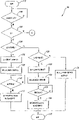
图4是表示用在图3的存储器件中的刷新控制器的操作的流程图。FIG. 4 is a flowchart representing the operation of a refresh controller used in the memory device of FIG. 3. Referring to FIG.

图5是包含图3和图4的存储器件的计算机系统的框图。FIG. 5 is a block diagram of a computer system including the memory device of FIGS. 3 and 4 .

具体实施方式 Detailed ways

下文描述在刷新DRAM中的存储单元期间可被访问的DRAM和方法。在描述中,阐述某些细节以便提供全面理解本发明的各种实施例。然而,对本领域的技术人员来说将容易理解的是,没有这些细节也可以实施本发明。在其他例子中,未详细地示出或描述公知电路、电路元件以及控制信号和相关的定时协议,以便避免不必要地使本发明的各种实施例的描述不明显。The DRAMs and methods that can be accessed during refreshing of memory cells in the DRAM are described below. In the description, certain details are set forth in order to provide a thorough understanding of various embodiments of the invention. It will be readily understood, however, to one skilled in the art that the present invention may be practiced without these details. In other instances, well-known circuits, circuit elements, and control signals and associated timing protocols have not been shown or described in detail in order to avoid unnecessarily obscuring the description of various embodiments of the invention.

本发明的优选实施例是在半导体管芯10上形成的一种DRAM,如图1所示。半导体管芯10包含多个存储体,存储体0、存储体1、存储体2...存储体N。每个存储体包含具有相同大小和存储相同数据位的两个存储器阵列12a、b。因而两个存储单元的存在是对于每个存储地址。因此,如果正刷新一个存储器阵列12a,可以在另一存储器阵列12b中发生对DRAM的存储访问。尽管在图1中示出的存储器阵列12a、b的布局是优选的,将理解的是,可以其他排列布置存储器阵列12a、b。The preferred embodiment of the present invention is a DRAM formed on a semiconductor die 10, as shown in FIG. Semiconductor die 10 includes a plurality of banks, Bank 0 , Bank 1 , Bank 2 . . . BankN. Each memory bank contains two memory arrays 12a, b of the same size and storing the same data bits. Thus two memory locations exist for each memory address. Thus, if one memory array 12a is being refreshed, a memory access to the DRAM may occur in the other memory array 12b. Although the layout of the memory arrays 12a,b shown in FIG. 1 is preferred, it will be appreciated that the memory arrays 12a,b may be arranged in other arrangements.

现在将参考图2描述访问阵列12a、b中对应的存储单元的方式。如本领域所公知的,每个阵列12a、b包含排列成行或列的多个存储单元(未示出)。为存储单元的每行提供行线(未示出),当一行激活时,允许存取行中的所有存储单元。通过经一对互补(complimentary)位线,将数据位耦合到存储单元或从存储单元耦合数据位,来访问被访问行中的特定存储单元,在图2中示出了其中的一对14a、b和16a、b。位线14a、b将数据耦合到相应阵列12a、b的一列或从相应的阵列12a、b的一列耦合数据,以及位线16a、b将数据的补码耦合到阵列12a、b的相同列或从阵列12a、b的相同列耦合数据的补码。为了清楚和简洁起见,已经省略了用于阵列12a、b的其他列的位线。The manner in which corresponding memory cells in the arrays 12a, b are accessed will now be described with reference to FIG. 2 . Each array 12a, b contains a plurality of memory cells (not shown) arranged in rows or columns, as is known in the art. A row line (not shown) is provided for each row of memory cells, allowing access to all memory cells in the row when a row is active. A particular memory cell in the row being accessed is accessed by coupling a data bit to or from the memory cell via a pair of complementary bit lines, of which a pair 14a, b and 16a,b. Bitlines 14a,b couple data to or from a column of a respective array 12a,b, and bitlines 16a,b couple the complement of the data to or from the same column of an array 12a,b. The complement of the data is coupled from the same column of the array 12a,b. The bit lines for the other columns of the arrays 12a, b have been omitted for clarity and conciseness.

如图2所示,通过相应的一组隔离晶体管22a、b、负读出放大器(“NSA”)24a、b、正读出放大器(“PSA”)26a、b以及相应的一组传输门晶体管28a、b,将位线14a、b和16a、b耦合到公共I/O电路20上。隔离晶体管22a、b以及读出放大器24、26的操作是常规的,因此为简洁起见,将省略对它们的完整说明。在写存储访问期间,通过数据通路(未示出),使数据耦合到I/O电路20。接通任何一组或两组传输门晶体管28a、b以便将数据耦合到阵列12a、b中任何一个或两个中的寻址行的寻址列中的存储单元。如果接通传输门晶体管组28a,则将数据写入存储器阵列12a。如果接通传输门晶体管组28b,则将数据写入存储器阵列12b。如果接通两个传输门晶体管组28b、b,则将数据写入两个存储器阵列12a、b。I/O 20电路最好包含能存储一行写数据的写缓冲器18。如果在对阵列的写访问期间正刷新阵列12a、b之一,则将数据暂时存储在I/O电路20的写缓冲器18中。在完成刷新后,将写数据从写缓冲器18传送到被刷新的阵列12a、b。另一方式是,在完成刷新后的稍后时间,可以将数据从阵列12a、b(数据被写入其中)传送到另一阵列12b、a。对于读访问,这些阵列中的一个(例如阵列12a)可被认为是主阵列,如果不是正在刷新阵列12a,将从该阵列读取数据。如果正在刷新阵列12a,那么可从阵列12b读取数据,于是将阵列12b认为是副阵列。另一方式是,可选择地将阵列12a、b的任一个当作主阵列,而将另一个作为副阵列。例如,在64ms的周期内,可以将阵列12a当作主阵列以及可以将阵列12b当作副阵列,64ms的周期是典型的刷新周期的持续时间。在下一个64ms内,可以将阵列12b作为主阵列以及可将阵列12a作为副阵列等等。在任何一种情况下,如果不是正刷新主阵列,则将从主阵列读取数据。如果正刷新主阵列,则从副阵列读取数据。最好通过刷新控制器(未示出)来控制传输门晶体管28a、b,刷新控制器将参考图3和4进行描述。As shown in FIG. 2, through a corresponding set of isolation transistors 22a,b, negative sense amplifiers (“NSA”) 24a,b, positive sense amplifiers (“PSA”) 26a,b, and a corresponding set of pass-gate transistors 28a, b, couple the bit lines 14a, b and 16a, b to the common I/O circuit 20 . The operation of isolation transistors 22a, b and sense amplifiers 24, 26 is conventional, so a full description of them will be omitted for the sake of brevity. During write memory accesses, data is coupled to I/O circuitry 20 through data paths (not shown). Either one or both sets of pass-gate transistors 28a,b are turned on to couple data to the memory cells in the addressed column of the addressed row in either or both arrays 12a,b. If transfer gate transistor group 28a is turned on, data is written to memory array 12a. If transfer gate transistor group 28b is turned on, data is written to memory array 12b. If both sets of pass-gate transistors 28b,b are turned on, data is written to both memory arrays 12a,b. The I/O 20 circuitry preferably includes a write buffer 18 capable of storing one row of write data. If one of the arrays 12a, b is being refreshed during a write access to the array, the data is temporarily stored in the write buffer 18 of the I/O circuit 20 . After the refresh is complete, the write data is transferred from the write buffer 18 to the array 12a,b being refreshed. Alternatively, data may be transferred from one array 12a,b (into which the data was written) to the other array 12b,a at a later time after the refresh is complete. For read accesses, one of these arrays (eg, array 12a) may be considered the primary array from which data will be read if array 12a is not being refreshed. If array 12a is being refreshed, data can be read from array 12b, and array 12b is then considered a secondary array. Alternatively, one of the arrays 12a, b can be selectively used as the primary array and the other as the secondary array. For example, array 12a may be considered as the primary array and array 12b may be considered as the secondary array during a period of 64ms, which is the duration of a typical refresh period. In the next 64 ms, array 12b can be used as the primary array and array 12a can be used as the secondary array, and so on. In either case, if the main array is not being flushed, the data will be read from the main array. If the primary array is being refreshed, data is read from the secondary array. Pass-gate transistors 28a,b are preferably controlled by a refresh controller (not shown), which will be described with reference to FIGS. 3 and 4 .

在读操作期间,读出放大器24a、b和26a、b在位线14、16上形成互补电压(complimentary voltage),其对应于正从存储器阵列12a、b的寻址行中的寻址列读取的数据。接通传输门晶体管28a、b之一组,以便将互补电压耦合到I/O电路20,然后经数据通路从I/O电路将其耦合。如果接通传输门晶体管组28a,从存储器阵列12a读取数据。如果接通传输门晶体管组28b,从存储器阵列12b读取数据。尽管不是同时从两个存储器阵列12a、b读取数据,可接通两个传输门晶体管28a、b,以便在从一个阵列12b、a的读操作之后、执行对另一个阵列12a、b的写操作。更具体地说,例如,可接通传输门晶体管28a来从存储器阵列12a读取数据。然后,在位线14a和16a上已形成对应于读取数据的电压,可接通传输门晶体管28b,以将正从存储器阵列12a读取的数据写入存储器阵列12b。During a read operation, sense amplifiers 24a,b and 26a,b develop complementary voltages on bit lines 14,16 corresponding to the voltage being read from the addressed column in the addressed row of memory array 12a,b. The data. One set of pass-gate transistors 28a, b is turned on to couple the complementary voltage to I/O circuit 20 and then from the I/O circuit via the data path. If transfer gate transistor group 28a is turned on, data is read from memory array 12a. If pass-gate transistor group 28b is turned on, data is read from memory array 12b. Although data is not being read from both memory arrays 12a,b at the same time, both pass gate transistors 28a,b can be turned on to perform a write to one array 12a,b after a read operation from the other array 12a,b operate. More specifically, for example, pass-gate transistor 28a may be turned on to read data from memory array 12a. Then, having developed a voltage on bit lines 14a and 16a corresponding to the read data, pass gate transistor 28b may be turned on to write the data being read from memory array 12a into memory array 12b.

尽管图2的实施例包括传输门晶体管28a、b,其特别设置用于将耦合数据到存储器阵列12a、b或从存储器阵列12a、b耦合数据,将理解的是,晶体管28a、b也可以是部分列寻址电路。假若这样的话,根据列地址和将被访问的阵列12a、b,接通晶体管28a、b。当然也可使用用于控制对阵列12a、b之任何一个的访问的其他电路。Although the embodiment of FIG. 2 includes pass-gate transistors 28a,b that are specifically configured to couple data to and from memory arrays 12a,b, it will be appreciated that transistors 28a,b may also be Partial column addressing circuitry. If so, transistors 28a,b are turned on depending on the column address and the array 12a,b to be accessed. Of course other circuitry for controlling access to either of the arrays 12a, b may also be used.

具有隐藏刷新的DRAM 40的一个实施例如图3所示。如在图1的DRAM中,DRAM 40包括N个存储体,每个存储体具有两个阵列12a、b。行和列地址用于访问阵列12a、b中的数据,它们通过地址总线42被施加到地址复用器44,以及通过控制总线46将命令信号施加到控制电路48,控制电路48包括内部命令译码器(未示出)。控制电路48生成各种控制信号用于控制DRAM 40的操作,下面将讨论其中一些控制信号。地址复用器44将行地址耦合到行译码器50以及将列地址耦合到用于阵列12a、b的相应列译码器52a、b。DRAM40还包括相应的读出放大器56a、b,如图2所示的负和正读出放大器24、26,以及相应的D.C.读出放大器(“DCSA”)和写驱动器(“WRITE”)58a、b(“DCSA/WRITE”)。DC读出放大器58a、b将从相应的读出放大器56a、b读取的数据耦合到数据通路电路60。数据通路电路60又将该读取的数据耦合到数据总线64。写数据被从数据总线64通过数据通路电路60耦合到写驱动器58a、b。写驱动器58a、b又将此数据耦合到如由列地址确定的互补对位线(在图3中未示出)。在图3的实施例中使用的这种D.C.读出放大器、写驱动器、以及数据通路电路的结构和操作是常规的。One embodiment of a DRAM 40 with hidden refresh is shown in FIG. 3 . As in the DRAM of FIG. 1 , the DRAM 40 includes N banks, each bank having two arrays 12a, b. Row and column addresses are used to access the data in the arrays 12a, b, they are applied to the address multiplexer 44 through the address bus 42, and the command signal is applied to the control circuit 48 through the control bus 46, the control circuit 48 includes the internal command translator encoder (not shown). Control circuitry 48 generates various control signals for controlling the operation of DRAM 40, some of which are discussed below. Address multiplexer 44 couples row addresses to row decoders 50 and column addresses to respective column decoders 52a,b for arrays 12a,b. DRAM 40 also includes respective sense amplifiers 56a, b, negative and positive sense amplifiers 24, 26 as shown in FIG. 2, and respective D.C. sense amplifiers ("DCSA") and write drivers ("WRITE") 58a, b ("DCSA/WRITE"). DC sense amplifiers 58a,b couple data read from respective sense amplifiers 56a,b to datapath circuitry 60 . Datapath circuitry 60 in turn couples the read data to data bus 64 . Write data is coupled from data bus 64 through datapath circuitry 60 to write drivers 58a,b. Write drivers 58a,b in turn couple this data to complementary pairs of bit lines (not shown in Figure 3) as determined by the column address. The structure and operation of the D.C. sense amplifier, write driver, and datapath circuitry used in the embodiment of FIG. 3 are conventional.

DARM 40还包括一组传输电路68,传输电路68可使用在图2的实施例中所示的传输门晶体管28来实现。传输电路68允许将数据从一个阵列12a、b的一列传送到另一阵列12b、a的对应列,如以上参考图2所述。DARM 40 also includes a set of pass circuits 68, which may be implemented using pass-gate transistors 28 shown in the embodiment of FIG. 2 . The transfer circuit 68 allows data to be transferred from one column of one array 12a, b to the corresponding column of the other array 12b, a, as described above with reference to FIG. 2 .

如前面所提到的,必须周期刷新存储器阵列12a、b中的存储单元以避免丢失数据。为此目的设置刷新控制器70。如在常规的刷新控制器中,刷新控制器70确保以足以防止丢失数据的速率刷新每个阵列12a、b中的每一行存储单元。然而,刷新控制器70能个别地刷新存储器阵列12a、b之任何一个,尽管它最好不同时刷新两个存储器阵列12a、b。如下详细所述,刷新控制器70的操作是根据存储器访问是写或读,因此它从控制电路48接收控制信号,包括读/写*(“R/W*”)信号。刷新控制器70也与数据有效寄存器74连接,如下详细所述,数据有效寄存器提供在阵列12a、b的每行中的数据是否有效的标记。寄存器74经刷新控制器70从地址复用器44接收行地址,以便当寻址存储器阵列12a、b的每行时,寄存器74能提供在每个阵列12a、b的寻址行中的数据是否有效的标记。As mentioned previously, the memory cells in the memory arrays 12a, b must be periodically refreshed to avoid loss of data. A refresh controller 70 is provided for this purpose. As in conventional refresh controllers, refresh controller 70 ensures that each row of memory cells in each array 12a, b is refreshed at a rate sufficient to prevent loss of data. However, refresh controller 70 can refresh either of memory arrays 12a, b individually, although it preferably does not refresh both memory arrays 12a, b simultaneously. As described in detail below, refresh controller 70 operates according to whether the memory access is a write or a read, and thus it receives control signals from control circuitry 48, including read/write* ("R/W*") signals. Refresh controller 70 is also coupled to a data valid register 74 which provides an indication of whether the data in each row of array 12a, b is valid or not, as described in detail below. Register 74 receives the row address from address multiplexer 44 via refresh controller 70 so that when addressing each row of memory array 12a,b, register 74 can provide whether the data in the addressed row of each array 12a,b is valid markup.

现在将参考如图4所示的流程图80,描述结合DARM 40之操作的刷新控制器70之操作。根据流程图80和常规刷新控制器电路的知识,由本领域的技术人员使用适当编程的微处理器(未示出)或硬布线逻辑电路(未示出),可以很容易实现在图3的实施例中采用的刷新控制器70。然而,应当注意,在流程图80和以下的说明中已经省略了DARM 40的许多操作步骤,因为它们是常规的而且与在此描述的发明原理关系不大。The operation of refresh controller 70 in conjunction with the operation of DARM 40 will now be described with reference to flowchart 80 shown in FIG. 4 . The implementation in FIG. 3 can be readily implemented by those skilled in the art using a suitably programmed microprocessor (not shown) or hardwired logic (not shown), based on the flowchart 80 and knowledge of conventional refresh controller circuitry. Refresh controller 70 used in the example. It should be noted, however, that many of the operational steps of the DARM 40 have been omitted in the flow diagram 80 and the following description, as they are conventional and have little to do with the inventive principles described herein.

参考图4,在100进入该过程,以刷新控制器70检测来自CPU(图3中未出)或其他存储器访问器件的存储器访问请求。控制电路48(图3)将合适的控制信号施加于刷新控制器70,以使刷新控制器70能够进行此确定。然后,刷新控制器70在102检验R/W*信号(图3)的状态,以确定存储器访问请求是否用于“写”存储器访问。如果检测到“写”请求,那么,刷新控制器70在104确定当前是否正在刷新主阵列。如上所述,阵列12a、b的任何一个可用作主阵列,或用作主阵列的阵列也可在阵列12a、b间交替。刷新控制器70能(做该决定)确定是否正在刷新阵列12a、b之任何一个,而不需要任何外部输入,因为刷新控制器70本身使得阵列12a、b被周期刷新。如果在104确定正在刷新主阵列,那么在106,将写数据写入副阵列的第R行,其中R是施加到地址复用器44的行地址。同样如上所述,可将阵列12a、b的任何一个用作主阵列,或用作主阵列的阵列也可在阵列12a、b间交替。(在此假定存储器访问是对阵列12a、b中的整行数据)。由除刷新控制器70以外的电路执行以这种方式对副阵列的数据写入,如上所述。然而,同样如上所述,刷新控制器70通过适当的手段选择主阵列或副阵列用于存储器访问,诸如通过控制如图2所示的传输门晶体管28a、b。在108,将写数据存储在写缓冲器18中,如上所述,写缓冲器18是在I/O电路20(图2)的内部。然后,刷新控制器70在110处的循环中等待完成主阵列的刷新,然后进行到112,在其中将存储在写缓冲器18中的数据传送给主阵列的第R行。因此,能将数据写入DARM 40而不需要CPU或其他存储器访问器件等待完成刷新。然后该过程经步骤116返回进入点100。Referring to FIG. 4, the process is entered at 100 to allow the refresh controller 70 to detect a memory access request from a CPU (not shown in FIG. 3) or other memory access device. Control circuitry 48 (FIG. 3) applies appropriate control signals to refresh controller 70 to enable refresh controller 70 to make this determination. Refresh controller 70 then checks the state of the R/W* signal (FIG. 3) at 102 to determine if the memory access request is for a "write" memory access. If a "write" request is detected, then refresh controller 70 determines at 104 whether the main array is currently being refreshed. As noted above, either of the arrays 12a, b can be used as the main array, or the array used as the main array can alternate between the arrays 12a, b. Refresh controller 70 can (make this determination) determine whether either of arrays 12a, b is being refreshed without requiring any external input, since refresh controller 70 itself causes arrays 12a, b to be periodically refreshed. If at 104 it is determined that the main array is being refreshed, then at 106 write data is written to the Rth row of the secondary array, where R is the row address applied to address multiplexer 44 . Also as noted above, either array 12a, b may be used as the main array, or the array used as the main array may alternate between arrays 12a, b. (It is assumed here that the memory access is to an entire row of data in the array 12a,b). Data writing to the sub-array in this manner is performed by circuits other than the refresh controller 70, as described above. However, as also described above, the refresh controller 70 selects either the main array or the sub-array for memory access by suitable means, such as by controlling the pass-gate transistors 28a, b as shown in FIG. 2 . At 108, the write data is stored in write buffer 18, which is internal to I/O circuitry 20 (FIG. 2), as described above. Refresh controller 70 then waits for completion of the refresh of the main array in a loop at 110 before proceeding to 112 where the data stored in write buffer 18 is transferred to row R of the main array. Thus, data can be written to the DARM 40 without requiring the CPU or other memory access device to wait for the refresh to complete. The process then returns to entry point 100 via step 116 .

如果刷新控制器70在104确定不是正在刷新主阵列,那么它在120进行检查来确定是否正在刷新副阵列。假若是的话,在步骤122将写数据写入主阵列的第R行,从而允许继续刷新副阵列。然后,在124将写数据存储在I/O电路20的写缓冲器18中。然后,在126的回路中,刷新控制器70等待完成副阵列的刷新,然后进行到128,在其中将存储在写缓冲器18中的数据传送到副阵列的第R行。然后,该过程经116再次返回100。If the refresh controller 70 determines at 104 that the primary array is not being refreshed, it checks at 120 to determine if the secondary array is being refreshed. If so, the write data is written to the Rth row of the main array at step 122, thereby allowing the secondary array to continue to be refreshed. The write data is then stored in write buffer 18 of I/O circuitry 20 at 124 . Then, in the loop at 126, the refresh controller 70 waits for the refresh of the sub-array to complete before proceeding to 128, where the data stored in the write buffer 18 is transferred to the Rth row of the sub-array. Then, the process returns to 100 again via 116 .

如果刷新控制器70在104确定不是正在刷新主阵列,并且它在120确定不是正在刷新副阵列,那么可将写数据写入两个阵列12a、b。因此,在130将写数据写入主阵列和副阵列12b的第R行,然后经116返回100。If the refresh controller 70 determines at 104 that the main array is not being refreshed, and it determines at 120 that the secondary array is not being refreshed, write data may be written to both arrays 12a,b. Therefore, at 130 the write data is written to the R-th row of the main array and the sub-array 12b, and then return to 100 via 116 .

如果在100检测到存储器访问请求后,刷新控制器70在102未检测“写”存储器访问请求,那么,它断定该请求必定是用于“读”存储器访问请求并进入步骤140。在140,刷新控制器70确定是否正在刷新主阵列,如果不是,刷新控制器70在步骤142使得从主阵列的第R行读取数据。然后,该过程经144返回步骤100。如果刷新控制器70在140确定不是正在刷新主阵列,在步骤146,它使得从副阵列的第R行读取数据,然后经144返回。刷新控制器可通过适当的手段选择用于存储器访问的主阵列或副阵列,诸如通过控制传输门晶体管28a、b(图2),以便将数据从主阵列读出而不是从副阵列,反之亦然。If after detecting a memory access request at 100, refresh controller 70 does not detect a "write" memory access request at 102, then it concludes that the request must be for a "read" memory access request and proceeds to step 140. At 140 , refresh controller 70 determines whether the main array is being refreshed, and if not, refresh controller 70 causes data to be read from row R of the main array at step 142 . The process then returns to step 100 via 144 . If the refresh controller 70 determines at 140 that the main array is not being refreshed, at step 146 it causes the data to be read from row R of the secondary array and then returns via 144 . The refresh controller can select either the main array or the sub-array for memory access by suitable means, such as by controlling pass-gate transistors 28a, b (FIG. 2) so that data is read from the main array instead of the sub-array, and vice versa. Of course.

参考图3和4描述的DRAM 40可有利地用在计算机系统中,如图5所示的计算机系统200。计算机系统200包括处理器202,其用于执行各种计算功能,如执行特定的软件来执行特定的计算或任务。处理器202包括处理器总线204,处理器总线通常包括地址总线206、控制总线208和数据总线210。另外,计算机系统200包括一个或多个输入设备214,如键盘或鼠标,以允许操作者与计算机系统200进行交互。通常,计算机系统200还包括连接处理器202的一个或多个输出设备216,这些输出设备通常是打印机或视频终端。通常也将一个或多个数据存储设备218连接到处理器202以存储数据或从外部存储介质(未示出)检索数据。典型的存储设备218的例子包括硬盘和软盘、盒式磁带以及光盘只读存储器(“CD-ROM”)。通常,处理器202还经存储控制器230连接到系统存储器228。系统存储器228通常由动态随机存取存储器(“DRAM”)组成。最后,计算机系统200包括超高速缓冲存储器236,它经处理器总线204连接到处理器202。如上所述,超高速缓冲存储器236通常是静态随机存取存储器(“SRAM”),它被设置用于使处理器202能够更快读取频繁存取或最近存取的数据或指令。然而,与常规的计算机系统不同的是,在图5的计算机系统200中所用的超高速缓冲存储器236是具有如图3和4所示的隐藏类型的DRAM。即使超高速缓冲存储器236要求两倍于相同容量的常规DRAM的存储单元,不过它使用相同容量的常规SRAM之一半数量的晶体管。因此,与用作超高速缓冲存储器236的SRAM相比,超高速缓冲存储器236能以相对很低的成本提供相对大的容量。The DRAM 40 described with reference to FIGS. 3 and 4 may be advantageously used in a computer system, such as the computer system 200 shown in FIG. 5 . The computer system 200 includes a processor 202 for performing various computing functions, such as executing specific software to perform specific calculations or tasks. Processor 202 includes a processor bus 204 which generally includes an address bus 206 , a control bus 208 and a data bus 210 . Additionally, computer system 200 includes one or more input devices 214 , such as a keyboard or mouse, to allow an operator to interact with computer system 200 . Typically, computer system 200 also includes one or more output devices 216 coupled to processor 202, typically a printer or a video terminal. One or more data storage devices 218 are also typically coupled to processor 202 for storing data or retrieving data from external storage media (not shown). Examples of typical storage devices 218 include hard and floppy disks, magnetic tape cassettes, and compact disk read-only memories ("CD-ROMs"). Typically, processor 202 is also coupled to system memory 228 via memory controller 230 . System memory 228 typically consists of dynamic random access memory ("DRAM"). Finally, computer system 200 includes cache memory 236 coupled to processor 202 via processor bus 204 . As noted above, cache memory 236 is typically static random access memory ("SRAM") configured to enable processor 202 to more quickly retrieve frequently or recently accessed data or instructions. However, unlike conventional computer systems, the cache memory 236 used in the computer system 200 of FIG. 5 is a DRAM of the hidden type as shown in FIGS. 3 and 4 . Even though cache memory 236 requires twice as many memory cells as conventional DRAM of the same capacity, it uses half the number of transistors as conventional SRAM of the same capacity. Therefore, the cache memory 236 can provide a relatively large capacity at a relatively low cost compared to the SRAM used as the cache memory 236 .

将理解的是,尽管为了说明的目的,已经描述过本发明的特定的实施例,但不脱离本发明的精神和范围,可能做出各种改变。例如,尽管在图4中以稍微基础的形式示出了DRAM 40,将理解到DRAM 40可能采用各种DRAM结构,包括同步DRAM(“SDRAM”)、存储器总线DRAM(“RDRAM”)以及同步链接DRAM(“SLDRAM”)。另外,尽管图5示出了由处理器202访问的DRAM40,将理解到也可使用其他访问设备,如图形处理器和其他直接存储器存取(“DMA”)器件。因此,本发明不是由公开的实施例来限定,而是由下述权利要求书来确定本发明的范围。It will be appreciated that, while specific embodiments of the invention have been described for purposes of illustration, various changes may be made without departing from the spirit and scope of the invention. For example, although DRAM 40 is shown in somewhat rudimentary form in FIG. DRAM ("SLDRAM"). Additionally, while FIG. 5 illustrates DRAM 40 being accessed by processor 202, it will be appreciated that other access devices, such as graphics processors and other direct memory access ("DMA") devices, may also be used. Accordingly, the invention is not limited by the disclosed embodiments, but rather the scope of the invention is determined by the following claims.

Claims (50)

1、一种动态随机存取存储器,包括:1. A dynamic random access memory, comprising: 第一阵列的存储单元;memory cells of the first array; 第二阵列的存储单元;memory cells of the second array; 地址电路,其接收一地址并被构成以访问对应于该地址的该第一和第二阵列中的位置;address circuitry receiving an address and configured to access locations in the first and second arrays corresponding to the address; 数据通路电路,被构成以在数据终端和第一及第二阵列之间耦合数据;datapath circuitry configured to couple data between the data terminals and the first and second arrays; 控制电路,其接收存储命令,并被构成以产生对应于所述存储命令的控制信号,以访问第一和第二阵列;以及a control circuit that receives a storage command and is configured to generate a control signal corresponding to the storage command to access the first and second arrays; and 刷新电路,其中该刷新电路包括刷新控制器,该刷新控制器被连接到该控制电路和该第一及第二阵列,该刷新控制器被构成以刷新该第一阵列或第二阵列中的存储单元,该刷新控制器被构成以使得当该第一或第二阵列正被刷新时、响应于写存储器访问而使写数据被临时存储在写缓冲器中,确定该刷新被完成之时,并在刷新完成后将该数据从该写缓冲器传送到被刷新的阵列中。Refresh circuit, wherein the refresh circuit includes a refresh controller, the refresh controller is connected to the control circuit and the first and second arrays, the refresh controller is configured to refresh the storage in the first array or the second array unit, the refresh controller configured such that when the first or second array is being refreshed, causing write data to be temporarily stored in a write buffer in response to a write memory access, determining when the refreshing is completed, and The data is transferred from the write buffer to the array being flushed after flushing is complete. 2、如权利要求1所述的动态随机存取存储器,其中,该控制电路被构成以生成响应写存储访问的第一组控制信号、以及响应读存储访问的第二组控制信号,其中,该刷新控制器进一步被构成以通过确定是否正在刷新该第一和第二阵列中的任一个,以及如果正在刷新第一和第二阵列中的一个、则允许数据被写入未被刷新的该第一和第二阵列中的一个,从而响应该第一组控制信号。2. The dynamic random access memory of claim 1, wherein the control circuit is configured to generate a first set of control signals responsive to a write memory access and a second set of control signals responsive to a read memory access, wherein the The refresh controller is further configured to allow data to be written to the unrefreshed first array by determining whether either of the first and second arrays is being refreshed, and if one of the first and second arrays is being refreshed. one and one of the second array, thereby responding to the first set of control signals. 3、如权利要求1所述的动态随机存取存储器,其中,该控制电路被构成以产生响应写存储访问的第一组控制信号、以及响应读存储访问的第二组控制信号,以及其中该刷新控制器被构成以通过确定是否正在刷新第一和第二阵列中的任何一个,以及如果第一和第二阵列都没有被正在刷新,则允许数据被写入第一和第二阵列,从而响应第一组控制信号。3. The dynamic random access memory of claim 1, wherein the control circuit is configured to generate a first set of control signals responsive to a write memory access, and a second set of control signals responsive to a read memory access, and wherein the The refresh controller is configured to allow data to be written to the first and second arrays by determining whether either of the first and second arrays is being refreshed, and if neither of the first and second arrays is being refreshed, thereby Respond to the first set of control signals. 4、如权利要求1所述的动态随机存取存储器,其中,该控制电路被构成以产生响应写存储访问的第一组控制信号、以及响应读存储访问的第二组控制信号,以及其中该刷新控制器被构成以通过确定是否正在刷新所述阵列之任一个,如果是则允许从未被刷新的阵列读取数据,从而响应第二组控制信号。4. The dynamic random access memory of claim 1, wherein the control circuit is configured to generate a first set of control signals responsive to a write memory access, and a second set of control signals responsive to a read memory access, and wherein the The refresh controller is configured to respond to the second set of control signals by determining whether any of the arrays are being refreshed, and if so, allowing data to be read from an array that is not being refreshed. 5、如权利要求1所述的动态随机存取存储器,其中,该控制电路被构成以产生响应写存储访问的第一组控制信号、以及响应读存储访问的第二组控制信号,以及其中该刷新控制器被构成以通过确定是否正在刷新所述阵列之任一个、以及如果两个阵列都没有被刷新则允许从所述阵列的一个主阵列读取数据,从而响应第二组控制信号。5. The dynamic random access memory of claim 1, wherein the control circuit is configured to generate a first set of control signals responsive to a write memory access, and a second set of control signals responsive to a read memory access, and wherein the The refresh controller is configured to respond to the second set of control signals by determining whether either of the arrays is being refreshed, and allowing data to be read from a main one of the arrays if neither array is being refreshed. 6、如权利要求5所述的动态随机存取存储器,其中,用作所述阵列之主阵列的阵列周期性在多个所述阵列之间交替。6. The dynamic random access memory of claim 5, wherein an array serving as a main array of said arrays alternates periodically among a plurality of said arrays. 7、如权利要求1所述的动态随机存取存储器,其中,第一和第二阵列每个包含多个具有对应于至少部分该地址的位置的位线对,以及其中第一阵列中的每个位线对通过传输电路连接到具有对应位置的第二阵列中的位线对,以及其中该刷新控制器被构成以通过断开对应于该地址的位线对之间的传输电路将数据写入所述阵列中。7. The dynamic random access memory of claim 1, wherein the first and second arrays each contain a plurality of bit line pairs having locations corresponding to at least part of the address, and wherein each of the first arrays A pair of bit lines is connected to a pair of bit lines in a second array having a corresponding position through a transmission circuit, and wherein the refresh controller is configured to write data by disconnecting the transmission circuit between the pair of bit lines corresponding to the address into the array. 8、如权利要求1所述的动态随机存取存储器,其中,该刷新控制器被进一步构成以根据是否正在刷新第一阵列以及是否正在刷新第二阵列的操作、控制对第一和第二阵列中的一个的访问。8. The dynamic random access memory as claimed in claim 1, wherein the refresh controller is further configured to control the operation of the first and second arrays according to whether the first array is being refreshed and whether the second array is being refreshed. one of the visits. 9、如权利要求1所述的动态随机存取存储器,其中,该动态随机存取存储器包括SDRAM。9. The dynamic random access memory of claim 1, wherein the dynamic random access memory comprises SDRAM. 10、如权利要求1所述的动态随机存取存储器,其中,该动态随机存取存储器包括RDRAM。10. The DRAM of claim 1, wherein the DRAM comprises RDRAM. 11、如权利要求1所述的动态随机存取存储器,其中,该动态随机存取存储器包括SLDRAM。11. The dynamic random access memory of claim 1, wherein the dynamic random access memory comprises SLDRAM. 12、如权利要求1所述的动态随机存取存储器,其中,该第一和第二阵列被包括在多个存储体的每一个中,以便每个存储体包含相应的一对第一和第二阵列。12. The dynamic random access memory of claim 1, wherein the first and second arrays are included in each of a plurality of memory banks such that each memory bank contains a corresponding pair of first and second Second array. 13、如权利要求12所述的动态随机存取存储器,其中,该动态随机存取存储器被制作在半导体晶片上,以及其中所述存储体被布置在该晶片上相应的离散区中,以便使每个离散区包含相应的一对第一和第二阵列。13. The dynamic random access memory of claim 12, wherein the dynamic random access memory is fabricated on a semiconductor wafer, and wherein said memory banks are arranged in respective discrete areas on the wafer so that Each discrete region contains a corresponding pair of first and second arrays. 14、一种动态随机存取存储器,包含:14. A dynamic random access memory, comprising: 第一阵列的存储单元,该第一阵列存储数据;memory cells of a first array, the first array storing data; 第二阵列的存储单元,该第二阵列包含与存储在该第一阵列中的数据相同的数据;memory cells of a second array, the second array containing the same data as the data stored in the first array; 地址电路,其接收一地址,以及被构成以访问对应于该地址的第一和第二阵列中的位置;address circuitry receiving an address and configured to access locations in the first and second arrays corresponding to the address; 数据通路电路,被构成以在数据终端和该第一及第二阵列之间耦合数据;datapath circuitry configured to couple data between data terminals and the first and second arrays; 控制电路;以及control circuits; and 刷新电路,其中该刷新电路包括刷新控制器,该刷新控制器被连接到该控制电路和第一及第二阵列,该刷新控制器被构成以刷新该第一阵列或第二阵列中的存储单元,以及该刷新控制器被构成以当正在刷新第二阵列时、允许数据被写入第一阵列,以及当正在刷新第一阵列时、允许数据被写入第二阵列。A refresh circuit, wherein the refresh circuit includes a refresh controller connected to the control circuit and the first and second arrays, the refresh controller configured to refresh memory cells in the first array or the second array , and the refresh controller is configured to allow data to be written to the first array while the second array is being refreshed, and to allow data to be written to the second array while the first array is being refreshed. 15、如权利要求14所述的动态随机存取存储器,其中,该刷新控制器进一步被构成以当正在刷新第一或第二阵列时、响应写存储访问而使得写数据被临时存储在写缓冲器中,确定完成该刷新之时,以及在该刷新完成后将该数据从该写缓冲器传送到被刷新的阵列中。15. The dynamic random access memory of claim 14, wherein the refresh controller is further configured to cause write data to be temporarily stored in the write buffer in response to a write memory access while the first or second array is being refreshed in the buffer, determine when the refresh is complete, and transfer the data from the write buffer to the refreshed array after the refresh is complete. 16、如权利要求14所述的动态随机存取存储器,其中,该刷新控制器被构成以确定第一和第二阵列是否均未被正在刷新,以及如果是的话则允许数据被写入第一和第二阵列。16. The dynamic random access memory of claim 14, wherein the refresh controller is configured to determine whether neither the first nor the second arrays are being refreshed, and if so, allow data to be written to the first and the second array. 17、如权利要求14所述的动态随机存取存储器,其中,该刷新控制器被进一步构成以当正在刷新第二阵列时、允许数据被写入第一阵列,以及当正在刷新第一阵列时、允许数据被写入第二阵列。17. The dynamic random access memory of claim 14, wherein the refresh controller is further configured to allow data to be written to the first array while the second array is being refreshed, and to allow data to be written to the first array when the first array is being refreshed , allowing data to be written to the second array. 18、如权利要求14所述的动态随机存取存储器,其中,该动态随机存取存储器包括SDRAM。18. The dynamic random access memory of claim 14, wherein the dynamic random access memory comprises SDRAM. 19、如权利要求14所述的动态随机存取存储器,其中,该第一和第二阵列被包含在多个存储体的每一个中,以便使每个存储体包含相应的一对第一和第二阵列。19. The dynamic random access memory of claim 14, wherein the first and second arrays are contained within each of a plurality of memory banks such that each memory bank contains a corresponding pair of first and second array. 20、如权利要求19所述的动态随机存取存储器,其中,该动态随机存取存储器被制作在半导体晶片上,以及其中所述存储体被布置在该晶片上相应的离散区中,以便使每个离散区包含相应的一对第一和第二阵列。20. The dynamic random access memory of claim 19, wherein the dynamic random access memory is fabricated on a semiconductor wafer, and wherein said memory banks are arranged in respective discrete areas on the wafer so that Each discrete region contains a corresponding pair of first and second arrays. 21、一种用于动态随机存取存储器的刷新电路,该存储器具有第一和第二阵列的存储单元,该电路包括:21. A refresh circuit for a dynamic random access memory having first and second arrays of memory cells, the circuit comprising: 刷新控制器,被构成以刷新该第一或第二阵列中的存储单元,该刷新控制器被构成以根据是否正在刷新第一阵列以及是否正在刷新第二阵列、来控制对第一和第二阵列中的一个的存取;以及a refresh controller configured to refresh memory cells in the first or second array, the refresh controller configured to control the first and second arrays according to whether the first array is being refreshed and whether the second array is being refreshed an access to one of the arrays; and 数据有效寄存器,被连接到该刷新控制器,该数据有效寄存器被构成以保留该第一和第二阵列的预定位置中存储的数据是否有效的标记。A data valid register is connected to the refresh controller, the data valid register is configured to hold a flag of whether the data stored in the predetermined positions of the first and second arrays is valid. 22、如权利要求21所述的刷新电路,其中,该刷新控制器被构成以通过确定是否正在刷新第一和第二阵列中的任何一个、以及如果正在刷新第一和第二阵列中的一个则允许数据被写入未被正在刷新的第一和第二阵列中的一个,从而响应写存储访问。22. The refresh circuit of claim 21, wherein the refresh controller is configured to determine whether either of the first and second arrays is being refreshed, and if one of the first and second arrays is being refreshed, Data is then allowed to be written to one of the first and second arrays that is not being refreshed, thereby responding to a write memory access. 23、如权利要求21所述的刷新电路,其中,该刷新控制器被构成以使得写数据被临时存储在写缓冲器中,确定完成该刷新之时,以及在该刷新完成后将写数据从该写缓冲器传送到被刷新的阵列中。23. The refresh circuit according to claim 21, wherein the refresh controller is configured such that the write data is temporarily stored in the write buffer, determines when the refresh is completed, and transfers the write data from the The write buffer is passed to the array to be flushed. 24、如权利要求21所述的刷新电路,其中,该刷新控制器被构成以通过确定是否正在刷新第一和第二阵列中的任何一个、以及如果第一和第二阵列均没有被正在刷新时则允许数据被写入第一和第二阵列,从而响应写存储访问。24. The refresh circuit of claim 21, wherein the refresh controller is configured to determine whether either of the first and second arrays is being refreshed, and if neither of the first and second arrays is being refreshed data is then allowed to be written to the first and second arrays in response to a write memory access. 25、如权利要求21所述的刷新电路,其中,该刷新控制器被构成以通过确定是否正在刷新所述阵列之任一个、以及如果是的话则允许从未被正在刷新的阵列读取数据,从而响应读存储访问。25. The refresh circuit of claim 21, wherein the refresh controller is configured to read data from the array not being refreshed by determining whether any of the arrays are being refreshed, and if so, allowing data to be read from the array that is not being refreshed, thus responding to read memory accesses. 26、如权利要求25所述的刷新电路,其中,该刷新控制器被构成以产生响应写存储访问的第一组控制信号、以及响应读存储访问的第二组控制信号,该刷新控制器被进一步构成以通过确定是否正在刷新所述阵列之任何一个、以及如果所述阵列均未被正在刷新则允许从所述阵列中的主阵列读取数据,从而响应该第二组控制信号。26. The refresh circuit of claim 25, wherein the refresh controller is configured to generate a first set of control signals responsive to a write memory access and a second set of control signals responsive to a read memory access, the refresh controller being controlled by It is further configured to respond to the second set of control signals by determining whether any of the arrays is being refreshed, and if none of the arrays is being refreshed, enabling data to be read from a primary of the arrays. 27、如权利要求26所述的刷新电路,其中,被用作所述阵列之主阵列的阵列周期性在多个所述阵列之间交替。27. The refresh circuit of claim 26, wherein the array used as the main array of said arrays alternates periodically between a plurality of said arrays. 28、如权利要求21所述的刷新电路,其中,该刷新控制器被构成以通过确定是否正在刷新第一和第二阵列中的任何一个、以及如果正在刷新第一和第二阵列的任何一个则允许从未被正在刷新的第一和第二阵列中的一个中读取数据,从而响应读存储访问。28. The refresh circuit of claim 21, wherein the refresh controller is configured to determine whether either of the first and second arrays is being refreshed, and if either of the first and second arrays is being refreshed, Data is then allowed to be read from one of the first and second arrays not being refreshed, thereby responding to a read memory access. 29、一种计算机系统,包括:29. A computer system comprising: 处理器,连接到处理器总线;a processor connected to the processor bus; 存储控制器,连接到处理器总线;a memory controller connected to the processor bus; 系统存储器,连接到存储控制器以便允许由该处理器进行存储器存取;a system memory connected to a memory controller to allow memory access by the processor; 数据输入设备,连接该处理器;a data input device connected to the processor; 数据输出设备,连接该处理器;以及a data output device coupled to the processor; and 超高速缓冲存储器,其通过处理器总线连接该处理器,该超高速缓冲存储器是一种动态随机存取存储器,包括:A cache memory, which is connected to the processor through a processor bus, is a dynamic random access memory, including: 第一阵列的存储单元;memory cells of the first array; 第二阵列的存储单元;memory cells of the second array; 地址电路,其接收一地址并被构成以访问对应于该地址的第一和第二阵列中的位置;address circuitry receiving an address and configured to access locations in the first and second arrays corresponding to the address; 数据通路电路,被构成以在数据终端和第一及第二阵列之间耦合数据;datapath circuitry configured to couple data between the data terminals and the first and second arrays; 控制电路,其接收存储命令,并被构成以产生对应于所述存储命令的控制信号,以访问该第一和第二阵列;以及a control circuit that receives a storage command and is configured to generate a control signal corresponding to said storage command to access the first and second arrays; and 刷新电路,其中该刷新电路包括刷新控制器,该刷新控制器连接该控制电路和第一及第二阵列,该刷新控制器被构成以刷新第一阵列或第二阵列中的存储单元,该刷新控制器被构成以使得当该第一或第二阵列正被刷新时、响应于写存储器访问而使写数据被临时存储在写缓冲器中,确定该刷新被完成之时,并在完成刷新后将该数据从该写缓冲器传送到被刷新的阵列中。A refresh circuit, wherein the refresh circuit includes a refresh controller, the refresh controller is connected to the control circuit and the first and second arrays, the refresh controller is configured to refresh the memory cells in the first array or the second array, the refresh The controller is configured such that the write data is temporarily stored in the write buffer in response to a write memory access while the first or second array is being refreshed, determines when the refresh is completed, and after completion of the refresh The data is transferred from the write buffer into the array being flushed. 30、如权利要求29所述的计算机系统,其中,该控制电路被构成以产生响应写存储访问的第一组控制信号、以及响应读存储访问的第二组控制信号,其中该刷新控制器进一步被构成以通过确定是否正在刷新第一和第二阵列中的任何一个、以及如果正在刷新第一和第二阵列中的一个则允许数据被写入未被正在刷新的第一和第二阵列中的一个,从而响应该第一组控制信号。30. The computer system of claim 29, wherein the control circuit is configured to generate a first set of control signals responsive to write memory accesses and a second set of control signals responsive to read memory accesses, wherein the refresh controller is further configured to allow data to be written to the first and second arrays that are not being refreshed by determining whether any of the first and second arrays is being refreshed, and if one of the first and second arrays is being refreshed one of the , thereby responding to the first set of control signals. 31、如权利要求29所述的计算机系统,其中,该控制电路被构成以产生响应写存储访问的第一组控制信号、以及响应读存储访问的第二组控制信号,以及其中该刷新控制器被构成以通过确定是否正在刷新第一和第二阵列中的任何一个、以及如果第一和第二阵列都没有被正在刷新则允许数据被写入第一和第二阵列,从而响应该第一组控制信号。31. The computer system of claim 29, wherein the control circuit is configured to generate a first set of control signals responsive to write memory accesses and a second set of control signals responsive to read memory accesses, and wherein the refresh controller Constructed to respond to the first group control signal. 32、如权利要求29所述的计算机系统,其中,该控制电路被构成以产生响应写存储访问的第一组控制信号、以及响应读存储访问的第二组控制信号,以及其中该刷新控制器被构成以通过确定是否正在刷新所述阵列之任何一个、以及如果所述两个阵列都没有被正在刷新则允许从所述阵列的主阵列读取数据,从而响应该第二组控制信号。32. The computer system of claim 29, wherein the control circuit is configured to generate a first set of control signals responsive to write memory accesses and a second set of control signals responsive to read memory accesses, and wherein the refresh controller configured to respond to the second set of control signals by determining whether either of the arrays is being refreshed, and enabling data to be read from a main array of the arrays if neither array is being refreshed. 33、如权利要求32所述的计算机系统,其中,被用作所述阵列的主阵列的阵列周期性在多个所述阵列之间交替。33. The computer system of claim 32, wherein the array used as the primary array of said array alternates periodically between a plurality of said arrays. 34、如权利要求32所述的计算机系统,其中,该第一和第二阵列每个包含多个位线对,其具有对应于至少部分地址的位置,以及其中第一阵列中的每个位线对通过传输电路被连接到具有对应位置的第二阵列中的位线对,以及其中该刷新控制器被构成以通过断开对应于该地址的位线对之间的传输电路将数据写入所述阵列中。34. The computer system of claim 32, wherein the first and second arrays each include a plurality of bit line pairs having locations corresponding to at least part of the address, and wherein each bit in the first array The line pair is connected to the bit line pair in the second array having a corresponding position through the transfer circuit, and wherein the refresh controller is configured to write data into the address by disconnecting the transfer circuit between the bit line pair corresponding to the address in the array. 35、如权利要求29所述的计算机系统,其中,该控制电路被构成以产生响应写存储访问的第一组控制信号、以及响应读存储访问的第二组控制信号,以及其中该刷新控制器通过确定是否正在刷新第一和第二阵列中的任何一个、以及如果正在刷新第一和第二阵列的任何一个则允许从未被正在刷新的第一和第二阵列中的一个中读取数据,从而响应该第二组控制信号。35. The computer system of claim 29, wherein the control circuit is configured to generate a first set of control signals responsive to a write memory access and a second set of control signals responsive to a read memory access, and wherein the refresh controller By determining whether any of the first and second arrays are being refreshed, and if any of the first and second arrays are being refreshed, allowing data to be read from one of the first and second arrays not being refreshed , thereby responding to the second set of control signals. 36、如权利要求29所述的计算机系统,其中,该刷新控制器进一步被构成以根据是否正在刷新第一阵列以及是否正在刷新第二阵列的操作、来控制对第一和第二阵列中的一个的访问。36. The computer system of claim 29, wherein the refresh controller is further configured to control operations on the first and second arrays based on whether the first array is being refreshed and whether the second array is being refreshed. A visit. 37、如权利要求29所述的计算机系统,其中,该动态随机存取存储器包括SDRAM。37. The computer system of claim 29, wherein the dynamic random access memory comprises SDRAM. 38、如权利要求29所述的计算机系统,其中,该动态随机存取存储器包括RDRAM。38. The computer system of claim 29, wherein the dynamic random access memory comprises RDRAM. 39、如权利要求29所述的计算机系统,其中,该动态随机存取存储器包括SLDRAM。39. The computer system of claim 29, wherein the dynamic random access memory comprises SLDRAM. 40、如权利要求29所述的计算机系统,其中,该第一和第二阵列被包括在多个存储体的每一个中,以便使每个存储体包含相应的一对第一和第二阵列。40. The computer system of claim 29, wherein the first and second arrays are included in each of a plurality of memory banks such that each memory bank contains a corresponding pair of first and second arrays . 41、如权利要求40所述的计算机系统,其中,该动态随机存取存储器被制作在半导体晶片上,以及其中所述存储体被布置在该晶片上相应的离散区中,以便使每个离散区包含相应的一对第一和第二阵列。41. The computer system of claim 40, wherein the DRAM is fabricated on a semiconductor die, and wherein said memory banks are arranged in respective discrete areas on the die such that each discrete A region contains a corresponding pair of first and second arrays. 42、一种刷新动态随机存取存储器同时隐藏该刷新的方法,该方法包括:42. A method for refreshing a dynamic random access memory while hiding the refreshing, the method comprising: 将数据存储在第一阵列的存储单元中;storing data in memory cells of the first array; 将与第一阵列的存储单元中存储的数据相同的数据存储在第二阵列的存储单元中,该第二阵列的存储单元的大小与第一阵列相同;storing the same data as the data stored in the memory cells of the first array in the memory cells of the second array, the memory cells of the second array having the same size as the first array; 刷新第一阵列或第二阵列中的存储单元,但不是同时刷新两个阵列;以及refreshing memory cells in either the first array or the second array, but not both arrays; and 根据是否正在刷新第一阵列以及是否正在刷新第二阵列的操作,允许对该第一和第二阵列中的一个进行存储器访问。Memory access to one of the first and second arrays is permitted based on the operation of whether the first array is being refreshed and whether the second array is being refreshed. 43、如权利要求42所述的方法,其中,该允许对该第一和第二阵列中的一个进行存储器访问的步骤包括:43. The method of claim 42, wherein the step of allowing memory access to the one of the first and second arrays comprises: 确定是否正在刷新该第一和第二阵列中的任何一个;以及determining whether any of the first and second arrays are being refreshed; and 如果正在刷新该第一和第二阵列中的一个时,允许数据被写入未被正在刷新的第一和第二阵列中的一个。If one of the first and second arrays is being refreshed, data is allowed to be written to the one of the first and second arrays that is not being refreshed. 44、如权利要求42所述的方法,其中,该允许对第一和第二阵列中的一个进行存储器访问的步骤包括:44. The method of claim 42, wherein the step of allowing memory access to one of the first and second arrays comprises: 确定是否正在刷新第一和第二阵列中的任何一个;以及determining whether any of the first and second arrays are being refreshed; and 如果第一和第二阵列均未被正在刷新时,允许数据被写入第一和第二阵列。Data is allowed to be written to the first and second arrays if neither of the first and second arrays is being refreshed. 45、如权利要求42所述的方法,其中,该允许对第一和第二阵列中的一个进行存储器访问的步骤包括:45. The method of claim 42, wherein the step of allowing memory access to one of the first and second arrays comprises: 确定是否正在刷新所述阵列之任何一个;determining whether any of the arrays are being refreshed; 如果正在刷新所述阵列之任何一个,允许从未被正在刷新的阵列读取数据;以及If any of the arrays is being refreshed, allowing data to be read from the array not being refreshed; and 如果所述两个阵列都未被正在刷新,允许从所述阵列之一个中读取数据。If neither array is being refreshed, data is allowed to be read from one of the arrays. 46、如权利要求42所述的方法,其中,如果所述两个阵列都未被正在刷新、则从其中读取数据的该阵列周期性地在所述阵列之间交替。46. The method of claim 42, wherein the array from which data is read is alternated between the arrays periodically if neither array is being refreshed. 47、如权利要求42所述的方法,其中,该允许对第一和第二阵列中的一个进行存储器访问的步骤包括:47. The method of claim 42, wherein the step of allowing memory access to one of the first and second arrays comprises: 确定是否正在刷新第一和第二阵列中的任何一个,以及determine whether any of the first and second arrays are being refreshed, and 如果正在刷新第一和第二阵列中的任何一个,允许从未被正在刷新的第一和第二阵列中的一个中读取数据。If either of the first and second arrays is being refreshed, data is allowed to be read from one of the first and second arrays that is not being refreshed. 48、一种刷新态随机存取存储器同时隐藏该刷新的方法,该方法包括:48. A method for refreshing a random access memory while hiding the refreshing, the method comprising: 将数据存储在第一阵列的存储单元中;storing data in memory cells of the first array; 将与第一阵列的存储单元中存储的数据相同的数据存储在第二阵列的存储单元中,该第二阵列的存储单元的大小与第一阵列相同;storing the same data as the data stored in the memory cells of the first array in the memory cells of the second array, the memory cells of the second array having the same size as the first array; 刷新第一阵列或第二阵列中的存储单元,但不是同时刷新两个阵列;refreshing memory cells in either the first array or the second array, but not both arrays; 当正在刷新第二阵列时,允许数据被写入第一阵列;以及allowing data to be written to the first array while the second array is being refreshed; and 当正在刷新第一阵列时,允许数据被写入第二阵列。Data is allowed to be written to the second array while the first array is being refreshed. 49、如权利要求48所述的方法,进一步包括:49. The method of claim 48, further comprising: 确定第一和第二阵列是否均未被正在刷新;以及determining whether neither the first nor the second array is being refreshed; and 如果该第一和第二阵列均未被正在刷新,则允许数据被写入第一和第二阵列。If neither of the first and second arrays is being refreshed, data is allowed to be written to the first and second arrays. 50、如权利要求48所述的方法,进一步包括:50. The method of claim 48, further comprising: 允许数据被写入第一或第二阵列后,把将被写入到正被刷新的阵列的数据临时存储在缓冲器中;temporarily storing data to be written to the array being refreshed in a buffer after allowing data to be written to the first or second array; 等待直到该阵列的刷新已被完成;以及wait until the refresh of the array has been completed; and 在该刷新已被完成后,允许该数据被写入该被刷新的阵列。After the flush has been completed, the data is allowed to be written to the flushed array.
CNB018174884A 2000-08-17 2001-08-14 Method and system for hiding refresh in dynamic random access memory Expired - Fee Related CN100570739C (en)

Applications Claiming Priority (2)

Application Number Priority Date Filing Date Title
US09/641,881 2000-08-17
US09/641,881 US6445636B1 (en) 2000-08-17 2000-08-17 Method and system for hiding refreshes in a dynamic random access memory

Publications (2)

Publication Number Publication Date
CN1471710A CN1471710A (en) 2004-01-28
CN100570739C true CN100570739C (en) 2009-12-16

Family

ID=24574243

Family Applications (1)

Application Number Title Priority Date Filing Date
CNB018174884A Expired - Fee Related CN100570739C (en) 2000-08-17 2001-08-14 Method and system for hiding refresh in dynamic random access memory

Country Status (9)

Country Link
US (1) US6445636B1 (en)
EP (2) EP2267722A1 (en)
JP (1) JP2004507856A (en)
KR (1) KR100796179B1 (en)
CN (1) CN100570739C (en)
AT (1) ATE484831T1 (en)
AU (1) AU2001283568A1 (en)
DE (1) DE60143268D1 (en)
WO (1) WO2002015194A1 (en)

Families Citing this family (22)

* Cited by examiner, † Cited by third party
Publication number Priority date Publication date Assignee Title
US6862654B1 (en) * 2000-08-17 2005-03-01 Micron Technology, Inc. Method and system for using dynamic random access memory as cache memory
US6697909B1 (en) * 2000-09-12 2004-02-24 International Business Machines Corporation Method and apparatus for performing data access and refresh operations in different sub-arrays of a DRAM cache memory
US6779076B1 (en) * 2000-10-05 2004-08-17 Micron Technology, Inc. Method and system for using dynamic random access memory as cache memory
TW523759B (en) * 2001-08-03 2003-03-11 Umax Data Systems Inc Circuit architecture with extended general purpose input/output pin
US7149824B2 (en) * 2002-07-10 2006-12-12 Micron Technology, Inc. Dynamically setting burst length of memory device by applying signal to at least one external pin during a read or write transaction
US7224631B2 (en) * 2004-08-31 2007-05-29 Micron Technology, Inc. Non-skipping auto-refresh in a DRAM
US20060190678A1 (en) * 2005-02-22 2006-08-24 Butler Douglas B Static random access memory (SRAM) compatible, high availability memory array and method employing synchronous dynamic random access memory (DRAM) in conjunction with a single DRAM cache and tag
US7506100B2 (en) * 2005-02-23 2009-03-17 United Memories, Inc. Static random access memory (SRAM) compatible, high availability memory array and method employing synchronous dynamic random access memory (DRAM) in conjunction with a data cache and separate read and write registers and tag blocks
US7123521B1 (en) 2005-04-27 2006-10-17 Micron Technology, Inc. Random cache read
US7313047B2 (en) * 2006-02-23 2007-12-25 Hynix Semiconductor Inc. Dynamic semiconductor memory with improved refresh mechanism
WO2009073512A1 (en) * 2007-11-29 2009-06-11 Dow Global Technologies Inc. Compounds and methods of forming compounds useful as a toner
US7408813B2 (en) * 2006-08-03 2008-08-05 Micron Technology, Inc. Block erase for volatile memory
JP4781229B2 (en) * 2006-11-01 2011-09-28 キヤノン株式会社 Distortion correction apparatus, imaging apparatus, and control method for distortion correction apparatus
KR100940868B1 (en) 2009-05-25 2010-02-09 이성재 Device realizing read characteristic of sram from dram and method of the same
CN102081964B (en) * 2009-11-30 2014-12-10 国际商业机器公司 Method and system for refreshing dynamic random access memory
TWI539453B (en) 2010-09-14 2016-06-21 半導體能源研究所股份有限公司 Memory device and semiconductor device
KR20130042236A (en) * 2011-10-18 2013-04-26 에스케이하이닉스 주식회사 Memory system
KR101970712B1 (en) * 2012-08-23 2019-04-22 삼성전자주식회사 Device and method for moving data in terminal
CN103700393B (en) 2012-09-28 2016-08-03 国际商业机器公司 Intermediate circuit and method for DRAM
CA3146951A1 (en) 2014-03-27 2015-10-01 Techtronic Power Tools Technology Limited Powered fastener driver and operating method thereof
US9824737B2 (en) 2015-12-22 2017-11-21 Intel Corporation Memory circuit and method for operating a first and a second set of memory cells in direct memory access mode with refresh
US10346093B1 (en) * 2018-03-16 2019-07-09 Xilinx, Inc. Memory arrangement for tensor data

Citations (2)

* Cited by examiner, † Cited by third party
Publication number Priority date Publication date Assignee Title
US5442588A (en) * 1994-08-16 1995-08-15 Cirrus Logic, Inc. Circuits and methods for refreshing a dual bank memory
US5999481A (en) * 1997-08-22 1999-12-07 Micron Technology, Inc. Method and apparatus for controlling the operation of an integrated circuit responsive to out-of-synchronism control signals

Family Cites Families (18)

* Cited by examiner, † Cited by third party
Publication number Priority date Publication date Assignee Title
JPS586232B2 (en) * 1977-09-21 1983-02-03 株式会社日立製作所 memory device
JPS5715286A (en) * 1980-06-30 1982-01-26 Toshiba Corp Memory device
JPS6257194A (en) * 1985-09-05 1987-03-12 Mitsubishi Electric Corp Duplex memory device
JPS63183694A (en) * 1987-01-23 1988-07-29 Mitsubishi Electric Corp semiconductor storage device
EP0420339A3 (en) * 1989-09-29 1992-06-03 N.V. Philips' Gloeilampenfabrieken Multi-plane random access memory system
EP0811979B1 (en) * 1990-12-25 2004-02-11 Mitsubishi Denki Kabushiki Kaisha A semiconductor memory device
JP3304531B2 (en) * 1993-08-24 2002-07-22 富士通株式会社 Semiconductor storage device
US5835436A (en) * 1995-07-03 1998-11-10 Mitsubishi Denki Kabushiki Kaisha Dynamic type semiconductor memory device capable of transferring data between array blocks at high speed
US5687132A (en) * 1995-10-26 1997-11-11 Cirrus Logic, Inc. Multiple-bank memory architecture and systems and methods using the same
JPH1011348A (en) * 1996-06-24 1998-01-16 Ricoh Co Ltd DRAM control device and its DRAM
US5835401A (en) * 1996-12-05 1998-11-10 Cypress Semiconductor Corporation Dram with hidden refresh
US5818777A (en) * 1997-03-07 1998-10-06 Micron Technology, Inc. Circuit for implementing and method for initiating a self-refresh mode
JP3490887B2 (en) * 1998-03-05 2004-01-26 シャープ株式会社 Synchronous semiconductor memory device
US5999474A (en) * 1998-10-01 1999-12-07 Monolithic System Tech Inc Method and apparatus for complete hiding of the refresh of a semiconductor memory
US6282606B1 (en) * 1999-04-02 2001-08-28 Silicon Aquarius, Inc. Dynamic random access memories with hidden refresh and utilizing one-transistor, one-capacitor cells, systems and methods
US6185136B1 (en) * 1999-07-15 2001-02-06 Micron Technology, Inc. Method and apparatus for repairing defective columns of memory cells
JP4555416B2 (en) * 1999-09-22 2010-09-29 富士通セミコンダクター株式会社 Semiconductor integrated circuit and control method thereof
JP3871853B2 (en) * 2000-05-26 2007-01-24 株式会社ルネサステクノロジ Semiconductor device and operation method thereof

Patent Citations (2)

* Cited by examiner, † Cited by third party
Publication number Priority date Publication date Assignee Title
US5442588A (en) * 1994-08-16 1995-08-15 Cirrus Logic, Inc. Circuits and methods for refreshing a dual bank memory
US5999481A (en) * 1997-08-22 1999-12-07 Micron Technology, Inc. Method and apparatus for controlling the operation of an integrated circuit responsive to out-of-synchronism control signals

Also Published As

Publication number Publication date
KR100796179B1 (en) 2008-01-21
ATE484831T1 (en) 2010-10-15
US6445636B1 (en) 2002-09-03
AU2001283568A1 (en) 2002-02-25
JP2004507856A (en) 2004-03-11
EP1328942A4 (en) 2008-01-02
EP1328942A1 (en) 2003-07-23
EP1328942B1 (en) 2010-10-13
EP2267722A8 (en) 2011-05-18
DE60143268D1 (en) 2010-11-25
EP2267722A1 (en) 2010-12-29
KR20030088020A (en) 2003-11-15
WO2002015194A1 (en) 2002-02-21
CN1471710A (en) 2004-01-28

Similar Documents

Publication Publication Date Title
CN100570739C (en) Method and system for hiding refresh in dynamic random access memory
US6958507B2 (en) Semiconductor memory pipeline buffer
US7206243B2 (en) Method of rewriting a logic state of a memory cell
US7917692B2 (en) Method and system for using dynamic random access memory as cache memory
EP0499256A1 (en) Semiconductor memory device
CN100433188C (en) Methods and Accessors for Multiple Word Line Access
KR100389750B1 (en) Semiconductor memory device that can access two regions alternately at high speed
US6330202B1 (en) Semiconductor memory device having write data line
JP2002008371A (en) Semiconductor storage device
US6975552B2 (en) Hybrid open and folded digit line architecture
KR100482380B1 (en) SRAM compatable memory having memory banks capable of indepedently writing access and Operating Method thereof
KR20040093895A (en) Semiconductor memory device for reducing peak current during refreshing operation
KR20130049150A (en) Reducing read disturbs and write fails in a data storage cell
KR100481820B1 (en) SRAM comPatible Memory Device comPensating an outPut data with Parity and OPerating Method thereof
JPS61126689A (en) Semiconductor memory device
TW411469B (en) Semiconductor memory with built-in row buffer and method of driving the same
JPH1173763A (en) Semiconductor integrated circuit device
CN116434798A (en) Memory device, operating method thereof, and memory system
KR20050013701A (en) Dual Port RAM having DRAM cell and being compatible with SRAM

Legal Events

Date Code Title Description
C06 Publication
PB01 Publication
C10 Entry into substantive examination
SE01 Entry into force of request for substantive examination
C14 Grant of patent or utility model
GR01 Patent grant
C17 Cessation of patent right
CF01 Termination of patent right due to non-payment of annual fee

Granted publication date: 20091216

Termination date: 20110814