CN100541784C - Stacked semiconductor chip package - Google Patents
Stacked semiconductor chip package Download PDFInfo
- Publication number
- CN100541784C CN100541784C CN200510117763.5A CN200510117763A CN100541784C CN 100541784 C CN100541784 C CN 100541784C CN 200510117763 A CN200510117763 A CN 200510117763A CN 100541784 C CN100541784 C CN 100541784C
- Authority
- CN
- China
- Prior art keywords
- semiconductor chip
- external connection
- several
- electrically connected
- mounting substrate
- Prior art date
- Legal status (The legal status is an assumption and is not a legal conclusion. Google has not performed a legal analysis and makes no representation as to the accuracy of the status listed.)
- Expired - Fee Related
Links
Images


Classifications
-
- H10W90/722—
-
- H10W90/724—
Landscapes
- Semiconductor Integrated Circuits (AREA)
Abstract
Description
技术领域 technical field
本发明涉及一种半导体芯片封装体,特别是涉及一种低轮廓堆叠式半导体芯片封装体。The invention relates to a semiconductor chip package, in particular to a low-profile stacked semiconductor chip package.
背景技术 Background technique
近年来,半导体芯片封装体的微型化及多功能化是为持续的趋势。为了满足此需求,芯片尺寸封装(CSP)技术及堆叠式封装技术是应运而生。就半导体内存芯片而言,若把两个规格相同的芯片堆叠在一起的话,则最终的内存封装体的内存容量得以增加。然而,半导体芯片被堆叠则势必导致整个封装体的高度增加,如此则有违微型化的趋势。In recent years, the miniaturization and multi-functionalization of semiconductor chip packages are a continuous trend. In order to meet this requirement, Chip Scale Package (CSP) technology and stacked package technology emerged as the times require. As far as semiconductor memory chips are concerned, if two chips with the same specification are stacked together, the memory capacity of the final memory package can be increased. However, the stacking of semiconductor chips will inevitably lead to an increase in the height of the entire package, which goes against the trend of miniaturization.
有鉴于此,本案发明人遂以其从事该行业的多年经验,并本着精益求精的精神,积极研究改良,遂有本发明『低轮廓堆叠式半导体芯片封装体』产生。In view of this, the inventor of this case actively researched and improved based on his many years of experience in this industry and in the spirit of excellence, and thus produced the "low-profile stacked semiconductor chip package" of the present invention.
发明内容 Contents of the invention
本发明的目的在于提供一种半导体芯片装置及其封装方法。The object of the present invention is to provide a semiconductor chip device and a packaging method thereof.
本发明的一特征在于:该堆叠式半导体芯片封装体包含:一第一半导体芯片,其具有一个上表面、一个下表面、及数个安装于该下表面上的外部连接导电体,于该第一半导体芯片的上表面和下表面上是分别布设有数条表面金属线,于该第一半导体芯片的下表面上的每条表面金属线是与一对应的外部连接导电体电连接;一第二半导体芯片,其具有一个下表面及数个安装于该下表面上的外部连接导电体,该第二半导体芯片安装于该第一半导体芯片的上表面上以致于该第二半导体芯片的外部连接导电体是与在该第一半导体芯片的上表面上的对应的表面金属线电连接;及数个U形金属元件,每个U形金属元件电连接在该第一半导体芯片的上表面上之一对应的表面金属线和在该第一半导体芯片的下表面上之一对应的表面金属线。A feature of the present invention is that the stacked semiconductor chip package includes: a first semiconductor chip, which has an upper surface, a lower surface, and a plurality of external connection conductors mounted on the lower surface. A plurality of surface metal wires are arranged on the upper surface and the lower surface of the semiconductor chip respectively, and each surface metal wire on the lower surface of the first semiconductor chip is electrically connected with a corresponding external connection conductor; a second A semiconductor chip having a lower surface and a plurality of external connection conductors mounted on the lower surface, the second semiconductor chip mounted on the upper surface of the first semiconductor chip so that the external connections of the second semiconductor chip are electrically conductive body is electrically connected with corresponding surface metal lines on the upper surface of the first semiconductor chip; and a plurality of U-shaped metal elements, each U-shaped metal element electrically connected to one of the upper surfaces of the first semiconductor chip A corresponding surface metal line and a corresponding surface metal line on the lower surface of the first semiconductor chip.
本发明的另一特征在于:该堆叠式半导体芯片封装体包含:一第一半导体芯片,其具有一个上表面、一个下表面、及数条分别布设于该上表面和下表面上的表面金属线;一第二半导体芯片,其具有一个下表面及数个安装于该下表面上的外部连接导电体,该第二半导体芯片安装于该第一半导体芯片的上表面上以致于该第二半导体芯片的外部连接导电体是与在该第一半导体芯片的上表面上的对应的表面金属线电连接;及数个U形金属元件,每个U形金属元件电连接在该第一半导体芯片的上表面上之一对应的表面金属线和在该第一半导体芯片的下表面上之一对应的表面金属线而且具有一个用于与外部电路电连接的外部电路连接部。Another feature of the present invention is that the stacked semiconductor chip package includes: a first semiconductor chip having an upper surface, a lower surface, and several surface metal wires respectively arranged on the upper surface and the lower surface ; a second semiconductor chip, which has a lower surface and several external connection conductors mounted on the lower surface, the second semiconductor chip is mounted on the upper surface of the first semiconductor chip so that the second semiconductor chip The external connection conductor is electrically connected with the corresponding surface metal line on the upper surface of the first semiconductor chip; and several U-shaped metal elements, each U-shaped metal element is electrically connected on the upper surface of the first semiconductor chip A corresponding one of the surface metal lines on the surface and a corresponding one of the surface metal lines on the lower surface of the first semiconductor chip have an external circuit connection portion for electrical connection with an external circuit.
本发明的另一特征在于:该堆叠式半导体芯片封装体包含:一第一半导体芯片,其具有一个上表面、一个下表面、及数个安装于该下表面上的外部连接导电体,于该第一半导体芯片的上表面和下表面上是分别布设有数条表面金属线,于该第一半导体芯片的下表面上的每条表面金属线是与一对应的外部连接导电体电连接,该第一半导体芯片更具有数个沿着其边缘设置的用于把在该上表面上的表面金属线电连接至在该下表面上的对应的表面金属线的导电半圆形孔;及一第二半导体芯片,其具有一个下表面及数个安装于该下表面上的外部连接导电体,该第二半导体芯片安装于该第一半导体芯片的上表面上以致于该第二半导体芯片的外部连接导电体是与在该第一半导体芯片的上表面上的对应的表面金属线电连接。Another feature of the present invention is that the stacked semiconductor chip package includes: a first semiconductor chip, which has an upper surface, a lower surface, and a plurality of external connection conductors mounted on the lower surface. Several surface metal wires are respectively arranged on the upper surface and the lower surface of the first semiconductor chip, and each surface metal wire on the lower surface of the first semiconductor chip is electrically connected with a corresponding external connecting conductor, the first semiconductor chip A semiconductor chip further has a plurality of conductive semicircular holes disposed along its edge for electrically connecting surface metal lines on the upper surface to corresponding surface metal lines on the lower surface; and a second A semiconductor chip having a lower surface and a plurality of external connection conductors mounted on the lower surface, the second semiconductor chip mounted on the upper surface of the first semiconductor chip so that the external connections of the second semiconductor chip are electrically conductive The bulk is electrically connected to a corresponding surface metal line on the upper surface of the first semiconductor chip.
本发明的另一特征在于:该堆叠式半导体芯片封装体包含:一基板,该基板具有一个上表面、一个下表面、一个矩形的容纳穿孔、及数个贯穿该上和下表面的电镀贯孔,于该上表面和下表面上是分别形成有数条导电金属连线,每条导电金属连线是自一对应的电镀贯孔延伸到界定该容纳穿孔的四个孔壁中之一者附近;一第一半导体芯片,其具有一个上表面、一个下表面、及数个安装于该下表面上的外部连接导电体,于该第一半导体芯片的上表面和下表面上是分别布设有数条表面金属线,于该第一半导体芯片的下表面上的每条表面金属线是与一对应的外部连接导电体电连接,该第一半导体芯片是安装于该基板的容纳穿孔内以致于在该第一半导体芯片的上表面上的每一条导电金属连线是与在该基板的上表面上之一对应的导电金属连线衔接而在该第一半导体芯片的下表面上的每一条导电金属连线是与在该基板的下表面上之一对应的导电金属连线衔接;一第二半导体芯片,其具有一个下表面及数个安装于该下表面上的外部连接导电体,该第二半导体芯片安装于该第一半导体芯片的上表面上以致于该第二半导体芯片的外部连接导电体是与在该第一半导体芯片的上表面上的对应的表面金属线电连接;及数个用于把在该第一半导体芯片的上和下表面上的导电金属连线电连接至在该基板的上和下表面上的对应的导电金属连线的U形金属元件。Another feature of the present invention is that the stacked semiconductor chip package includes: a substrate, the substrate has an upper surface, a lower surface, a rectangular receiving through hole, and several plated through holes penetrating the upper and lower surfaces , on the upper surface and the lower surface, a plurality of conductive metal connection lines are respectively formed, and each conductive metal connection line extends from a corresponding plated through hole to the vicinity of one of the four hole walls defining the receiving through hole; a first A semiconductor chip, which has an upper surface, a lower surface, and several external connection conductors installed on the lower surface, and several surface metal wires are respectively arranged on the upper surface and the lower surface of the first semiconductor chip , each surface metal line on the lower surface of the first semiconductor chip is electrically connected to a corresponding external connection conductor, the first semiconductor chip is mounted in the receiving through hole of the substrate so that the first semiconductor chip Each conductive metal connection on the upper surface of the chip is connected to a corresponding conductive metal connection on the upper surface of the substrate and each conductive metal connection on the lower surface of the first semiconductor chip is connected to A corresponding conductive metal connection on the lower surface of the substrate is connected; a second semiconductor chip has a lower surface and a plurality of external connection conductors mounted on the lower surface, the second semiconductor chip is mounted on On the upper surface of the first semiconductor chip so that the external connection conductors of the second semiconductor chip are electrically connected to the corresponding surface metal lines on the upper surface of the first semiconductor chip; The conductive metal wires on the upper and lower surfaces of the first semiconductor chip are electrically connected to the U-shaped metal elements of the corresponding conductive metal wires on the upper and lower surfaces of the substrate.
附图说明 Description of drawings
下面结合附图及实施例对本发明堆叠式半导体芯片封装体进行详细说明:The stacked semiconductor chip package of the present invention will be described in detail below in conjunction with the accompanying drawings and embodiments:
图1至图4是为显示本发明的第一较佳实施例的堆叠式半导体芯片封装体的示意图;1 to 4 are schematic diagrams showing a stacked semiconductor chip package according to a first preferred embodiment of the present invention;
图5至图8是为显示本发明的第二较佳实施例的堆叠式半导体芯片封装体的示意图;5 to 8 are schematic diagrams showing a stacked semiconductor chip package according to a second preferred embodiment of the present invention;
图9和10是为显示本发明的第三较佳实施例的堆叠式半导体芯片封装体的示意图;9 and 10 are schematic diagrams showing a stacked semiconductor chip package according to a third preferred embodiment of the present invention;
图11至14是为显示本发明的第四较佳实施例的堆叠式半导体芯片封装体的示意图;11 to 14 are schematic diagrams showing a stacked semiconductor chip package according to a fourth preferred embodiment of the present invention;
图15是为一个显示本发明的第五较佳实施例的堆叠式半导体芯片封装体的示意侧视图;15 is a schematic side view showing a stacked semiconductor chip package according to a fifth preferred embodiment of the present invention;
图16是为一个显示本发明的第六较佳实施例的堆叠式半导体芯片封装体的示意侧视图;16 is a schematic side view showing a stacked semiconductor chip package according to a sixth preferred embodiment of the present invention;
图17是为一个显示本发明的第七较佳实施例的堆叠式半导体芯片封装体的示意侧视图;17 is a schematic side view showing a stacked semiconductor chip package according to a seventh preferred embodiment of the present invention;
图18是为一个显示本发明的第八较佳实施例的堆叠式半导体芯片封装体的示意侧视图;18 is a schematic side view showing a stacked semiconductor chip package according to an eighth preferred embodiment of the present invention;
图19是为一个显示本发明的第九较佳实施例的堆叠式半导体芯片封装体的示意侧视图;及19 is a schematic side view showing a stacked semiconductor chip package of a ninth preferred embodiment of the present invention; and
图20是为一个显示本发明的第十较佳实施例的堆叠式半导体芯片封装体的示意侧视图。FIG. 20 is a schematic side view showing a stacked semiconductor chip package according to a tenth preferred embodiment of the present invention.
具体实施方式 Detailed ways
为了方便说明,以下的实施例,相同的元件以相同标号表示。For the convenience of description, in the following embodiments, the same components are denoted by the same reference numerals.
参阅图1至图4,本发明的第一较佳实施例的堆叠式半导体芯片封装体包括一基板1、一第一半导体芯片2、及一第二半导体芯片3。Referring to FIGS. 1 to 4 , a stacked semiconductor chip package according to a first preferred embodiment of the present invention includes a
基板1具有一个上表面10、一个下表面11、一个矩形的容纳穿孔12、及数个贯穿上和下表面10和11的电镀贯孔13。数条第一导电金属连线14是形成于基板1的上表面10上。每条第一导电金属连线14是自一对应的电镀贯孔13延伸到界定该容纳穿孔12的四个孔壁中之一附近。The
数条第二导电金属连线15是形成于基板1的下表面11上。每条第二导电金属连线15是自一对应的电镀贯孔13延伸到界定该容纳穿孔12的四个孔壁中之一附近。该等第一导电金属连线14是经由对应的电镀贯孔13来与对应的第二导电金属连线15电连接。Several second
该第一半导体芯片2具有一个上表面20、一个下表面21、及数个安装于下表面21上的外部连接导电体22。数条第三表面金属线23是形成于第一半导体芯片2的上表面20上。每条第三表面金属线23是自芯片2的边缘延伸到一个相当于一对应的外部连接导电体22的位置。The
数条第四表面金属线24是形成于第一半导体芯片2的下表面21上。每条第四表面金属线24是自该芯片2的边缘延伸到一对应的外部连接导电体22以可与对应的外部连接导电体22电连接。Several fourth
该第一半导体芯片2是安装于基板1的容纳穿孔12内以致于在第一半导体芯片2的上表面20上的每一条第三表面金属线23是与在基板1的上表面10上之一对应的第一导电金属连线14衔接而在第一半导体芯片2的下表面21上的每一条第四表面金属线24是与在基板1的下表面11上之一对应的第二导电金属连线15衔接。The
为了确保在该第一半导体芯片2的上和下表面20和21上的第三和第四表面金属线23和24与在基板1的上和下表面10和11上的对应的第一和第二导电金属连线14和15之间的可靠电连接,每两条对应的表面金属线23,24,14和15是由一U形金属元件4(图未示)连接。该等U形金属元件4可以由任何适合的导电金属材料制成,例如,锡膏、银胶、导电金属胶、导线等等。In order to ensure that the third and fourth
第二半导体芯片3具有一个下表面31及数个安装于下表面31上的外部连接导电体32。第二半导体芯片3是安装于第一半导体芯片2的上表面20上以致于第二半导体芯片3的外部连接导电体32是与在第一半导体芯片2的上表面20上的对应的第三表面金属线23电连接。如是,该第二半导体芯片3的内部电路能够经由该等外部连接导电体32、该等第三表面金属线23、该等电镀贯孔13、该等第四表面金属线24、和该等外部连接导电体22来与外部电路电连接。The
一个绝缘保护层5(见图1)是形成于基板1的上表面10上在第二半导体芯片3四周。该绝缘保护层5的作用是在于稳固该第一和第二半导体芯片2和3及防止会影响该第一与第二半导体芯片2与3之间的电连接的湿气入侵。An insulating protective layer 5 (see FIG. 1 ) is formed on the
应要注意的是,于第二半导体芯片3的上表面上也可以布设有与在第一半导体芯片2的上表面20上的导电金属线,类似的导电金属线以可进一步叠置另一半导体芯片于其上。或者,端视需要而定,于第二半导体芯片3的上表面上是可布设有任何需要的电路轨迹,例如,具有电波接收与发射的功能的天线回路、任何生物侦测探针或感应元件形成回路等等。It should be noted that on the upper surface of the
另一方面,第一半导体芯片2和第二半导体芯片3的大小、类型、及功能等等可以是不相同的。On the other hand, the size, type, function, etc. of the
参阅图5至图8,本发明的第二较佳实施例的堆叠式半导体芯片封装体包括一第一半导体芯片2和一第二半导体芯片3。Referring to FIG. 5 to FIG. 8 , the stacked semiconductor chip package according to the second preferred embodiment of the present invention includes a
第一半导体芯片2具有一个上表面20、一个下表面21、及数个安装于下表面21上的外部连接导电体22。数条第三表面金属线23是形成于第一半导体芯片2的上表面20上。每条第三表面金属线23是自芯片2的边缘延伸到一个相当于一对应的外部连接导电体22的位置。The
数条第四表面金属线24是形成于第一半导体芯片2的下表面21上。每条第四表面金属线24是自芯片2的边缘延伸到一对应的外部连接导电体22而可与对应的外部连接导电体22电连接。Several fourth
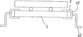
在第一半导体芯片2的上表面20上的每一条第三表面金属线23是经由一个U形金属元件4’来与在下表面21上之一对应的第四表面金属线24电连接。在本实施例中,该等U形金属元件4’是为大致U形的金属片而且每个U形金属元件4’具有一个置于第一半导体芯片2的上表面20上以可与一对应的第三表面金属线23电连接的第一臂部40’、一个置于第一半导体芯片2的下表面21上以可与一对应的第四表面金属线24电连接的第二臂部41’、及一个连接第一臂部40’和第二臂部41’的臂连接部42’。Each third
该第二半导体芯片3具有一个下表面31及数个安装于下表面31上的外部连接导电体32。该第二半导体芯片3是安装于第一半导体芯片2的上表面20上以致于第二半导体芯片3的外部连接导电体32是与在第一半导体芯片2的上表面20上的对应的第三表面金属线22电连接。如是,该第二半导体芯片3的内部电路能够经由等外部连接导电体32、该等第三表面金属线23、该等U形金属元件4’、该等第四表面金属线24、和该等外部连接导电体22来与外部电路电连接。The
参阅图9至图10,是为一个显示本发明的第三较佳实施例,与第二较佳实施例不同的是,每个U形金属元件4’更包括一个自臂连接部42’延伸出来以可与外部电路(图中未示)电连接的外部电路连接部43’。由于该等外部电路连接部43’的设置,于在第二较佳实施例中所示的第一半导体芯片2的下表面上的导电金属连线及外部连接导电体(见第八图)是可免除。Referring to Fig. 9 to Fig. 10, it is a third preferred embodiment showing the present invention, and the difference from the second preferred embodiment is that each U-shaped metal element 4' further includes an arm connecting portion 42' extending An external circuit connection portion 43' that can be electrically connected to an external circuit (not shown in the figure) is provided. Due to the setting of these external circuit connection parts 43', the conductive metal wirings and external connection conductors (see the eighth figure) on the lower surface of the
参阅图11至图14,本发明的第四较佳实施例的堆叠式半导体芯片封装体包括一第一半导体芯片2及一第二半导体芯片3。Referring to FIG. 11 to FIG. 14 , the stacked semiconductor chip package according to the fourth preferred embodiment of the present invention includes a
该第一半导体芯片2具有一个上表面20、一个下表面21、数个安装于下表面21上的外部连接导电体22、及数个沿着第一半导体芯片2的边缘设置的导电半圆形孔25。该等导电半圆形孔25的形成可以是借着在该第一半导体芯片2自一片晶圆切割出来之前先沿着切割线钻孔并电镀形成电镀贯孔而然后再沿切割线切割来被形成。当然,该等导电半圆形孔25也可以借着任何其它适当的手段来被形成,例如,以导电胶填充以形成导电胶-填充贯孔来代替以电镀形成电镀贯孔。The
数条第三表面金属线23是形成于该第一半导体芯片2的上表面20上。每条第三表面金属线23是自一个相当于一对应的外部连接导电体22的位置延伸到一个对应的导电半圆形孔25。Several third
数条第四表面金属线24是形成于第一半导体芯片2的下表面21上。每条第四表面金属线24是自一个对应的外部连接导电体22延伸到一个对应的导电半圆形孔25以可与对应的外部连接导电体22电连接。Several fourth
该第二半导体芯片3具有一个下表面31及数个安装于下表面31上的外部连接导电体32。第二半导体芯片3是安装于第一半导体芯片2的上表面20上以致于第二半导体芯片3的外部连接导电体32是与在第一半导体芯片2的上表面20上的对应的第三表面金属线23电连接。如是,该第二半导体芯片3的内部电路能够经由该等外部连接导电体32、该等第三表面金属线23、该等第四表面金属线24、和该等外部连接导电体22来与外部电路电连接。The
参阅图15,本发明的第五较佳实施例包括一基板1’、一第一半导体芯片2、一第二半导体芯片3、及一保护层5。Referring to FIG. 15, a fifth preferred embodiment of the present invention includes a substrate 1', a
该基板1’具有一个上表面10、一个下表面11、数个贯穿该上和下表面10和11的电镀贯孔13、及数个设置于基板1’的下表面11上的外部连接导电体14。数条与第一较佳实施例相似的第一导电金属连线(图中未示)是形成于基板1’的上表面10上。每条第一导电金属连线是自一对应的电镀贯孔13延伸到一预定的位置。The substrate 1' has an
数条与第一较佳实施例相似的第二导电金属连线(图中未示)是形成于基板1’Several second conductive metal connections (not shown) similar to the first preferred embodiment are formed on the substrate 1'
数条与第一较佳实施例相似的第二导电金属连线(图中未示)是形成于基板1’的下表面11上。每条第二导电金属连线是自一对应的电镀贯孔13延伸到一对应的外部连接导电体14以可与该对应的外部连接导电体14电连接。该等第一导电金属连线14是经由对应的电镀贯孔13来与对应的第二导电金属连线电连接。Several second conductive metal wires (not shown) similar to the first preferred embodiment are formed on the
该第一半导体芯片2是与在第四较佳实施例中所示的相同而因此,其详细描述于此恕不再赘述。第一半导体芯片2是被设置于基板1’的上表面10上以致于该第一半导体芯片2的外部连接导电体22(见图14)是与在该基板1’的上表面10上的第一导电金属连线电连接。The
该第二半导体芯片3是与在第四较佳实施例中所示的相同而且是以与在第四较佳实施例中所述的形式相同的形式设置于第一半导体芯片2上。The
绝缘保护层5是形成于基板1’的上表面10上以可覆盖该等半导体芯片2和3。An insulating
参阅图16,是为一个显示本发明的第六较佳实施例,与第五较佳实施例不同的是,本较佳实施例包含四个堆叠设置的半导体芯片。Referring to FIG. 16 , it shows a sixth preferred embodiment of the present invention. The difference from the fifth preferred embodiment is that this preferred embodiment includes four stacked semiconductor chips.
参阅图17,本发明的第七较佳实施例包括一第一基板1’、一第二基板6、一第三基板7、一第一半导体芯片2、一第二半导体芯片3、及一保护层5。Referring to Fig. 17, the seventh preferred embodiment of the present invention comprises a first substrate 1', a second substrate 6, a third substrate 7, a
该基板1’是与在第五较佳实施例中所述的相同而因此其详细描述于此不再赘述。The substrate 1' is the same as that described in the fifth preferred embodiment and thus its detailed description will not be repeated here.
该第二基板6是与在第一较佳实施例中所述的相同而因此其详细描述于此不再赘述。The second substrate 6 is the same as that described in the first preferred embodiment and thus its detailed description will not be repeated here.
该第一半导体芯片2是与在第一较佳实施例中所示的相同而且是以与在第一较佳实施例中所述相同的形式安装于第二基板6,因此,其详细描述于此恕不再赘述。The
该第三基板7是与第二基板6相同而因此其详细描述于此不再赘述。The third substrate 7 is the same as the second substrate 6 and thus its detailed description will not be repeated here.
该第二半导体芯片3是与在第一较佳实施例中所示的相同而且是以与在第一较佳实施例中所述的形式相同的形式安装于第三基板7及设置于第一半导体芯片2上。The
该绝缘保护层5是形成于基板1’的上表面10上以可覆盖等半导体芯片2和3。The insulating
参阅图18,是本发明的第八较佳实施例,与第七较佳实施例不同的是,本较佳实施例包含四个堆叠设置的半导体芯片。Referring to FIG. 18 , it is the eighth preferred embodiment of the present invention. The difference from the seventh preferred embodiment is that this preferred embodiment includes four stacked semiconductor chips.
参阅图19,是本发明的第九较佳实施例,本较佳实施例包括一基板1’、一第一半导体芯片2、一第二半导体芯片3、及一保护层5。Referring to Fig. 19, it is the ninth preferred embodiment of the present invention. This preferred embodiment includes a substrate 1', a
该基板1’是与在第五较佳实施例中所述的相同而因此其详细描述于此不再赘述。The substrate 1' is the same as that described in the fifth preferred embodiment and thus its detailed description will not be repeated here.
该第一半导体芯片2和该第二半导体芯片3是与在第二较佳实施例中所示的相同而且是以与在第二较佳实施例中所述的相同的形式堆叠并且设置于基板1’上,因此,其详细描述于此恕不再赘述。The
该绝缘保护层5是形成于基板1’的上表面10上以可覆盖等半导体芯片2和3。The insulating
参阅图20,是为本发明的第十较佳实施例,与第九较佳实施例不同的是,本较佳实施例包含四个堆叠设置的半导体芯片。Referring to FIG. 20 , it is the tenth preferred embodiment of the present invention. The difference from the ninth preferred embodiment is that this preferred embodiment includes four semiconductor chips stacked.
Claims (12)
Priority Applications (1)
| Application Number | Priority Date | Filing Date | Title |
|---|---|---|---|
| CN200510117763.5A CN100541784C (en) | 2005-11-10 | 2005-11-10 | Stacked semiconductor chip package |
Applications Claiming Priority (1)
| Application Number | Priority Date | Filing Date | Title |
|---|---|---|---|
| CN200510117763.5A CN100541784C (en) | 2005-11-10 | 2005-11-10 | Stacked semiconductor chip package |
Publications (2)
| Publication Number | Publication Date |
|---|---|
| CN1964037A CN1964037A (en) | 2007-05-16 |
| CN100541784C true CN100541784C (en) | 2009-09-16 |
Family
ID=38083022
Family Applications (1)
| Application Number | Title | Priority Date | Filing Date |
|---|---|---|---|
| CN200510117763.5A Expired - Fee Related CN100541784C (en) | 2005-11-10 | 2005-11-10 | Stacked semiconductor chip package |
Country Status (1)
| Country | Link |
|---|---|
| CN (1) | CN100541784C (en) |
Families Citing this family (1)
| Publication number | Priority date | Publication date | Assignee | Title |
|---|---|---|---|---|
| US8896112B2 (en) * | 2013-03-15 | 2014-11-25 | Oracle International Corporation | Multi-chip module with self-populating positive features |
Citations (8)
| Publication number | Priority date | Publication date | Assignee | Title |
|---|---|---|---|---|
| US20010054758A1 (en) * | 2000-06-21 | 2001-12-27 | Isaak Harlan R. | Three-dimensional memory stacking using anisotropic epoxy interconnections |
| US6469395B1 (en) * | 1999-11-25 | 2002-10-22 | Mitsubishi Denki Kabushiki Kaisha | Semiconductor device |
| US20030232486A1 (en) * | 2002-06-14 | 2003-12-18 | Shinko Electric Industries Co., Ltd. | Semiconductor device and method of manufacturing the same |
| US6768190B2 (en) * | 2002-01-25 | 2004-07-27 | Advanced Semiconductor Engineering, Inc. | Stack type flip-chip package |
| US20040217485A1 (en) * | 2003-05-02 | 2004-11-04 | Advanced Semiconductor Engineering Inc. | Stacked flip chip package |
| US20050035441A1 (en) * | 2003-08-15 | 2005-02-17 | Kwanghak Lee | Integrated circuit stack with partially etched lead frames |
| US20050133932A1 (en) * | 2003-12-19 | 2005-06-23 | Jens Pohl | Semiconductor module with a semiconductor stack, and methods for its production |
| US20050205982A1 (en) * | 2004-03-19 | 2005-09-22 | Nec Electronics Corporation | Semiconductor device |
-
2005
- 2005-11-10 CN CN200510117763.5A patent/CN100541784C/en not_active Expired - Fee Related
Patent Citations (8)
| Publication number | Priority date | Publication date | Assignee | Title |
|---|---|---|---|---|
| US6469395B1 (en) * | 1999-11-25 | 2002-10-22 | Mitsubishi Denki Kabushiki Kaisha | Semiconductor device |
| US20010054758A1 (en) * | 2000-06-21 | 2001-12-27 | Isaak Harlan R. | Three-dimensional memory stacking using anisotropic epoxy interconnections |
| US6768190B2 (en) * | 2002-01-25 | 2004-07-27 | Advanced Semiconductor Engineering, Inc. | Stack type flip-chip package |
| US20030232486A1 (en) * | 2002-06-14 | 2003-12-18 | Shinko Electric Industries Co., Ltd. | Semiconductor device and method of manufacturing the same |
| US20040217485A1 (en) * | 2003-05-02 | 2004-11-04 | Advanced Semiconductor Engineering Inc. | Stacked flip chip package |
| US20050035441A1 (en) * | 2003-08-15 | 2005-02-17 | Kwanghak Lee | Integrated circuit stack with partially etched lead frames |
| US20050133932A1 (en) * | 2003-12-19 | 2005-06-23 | Jens Pohl | Semiconductor module with a semiconductor stack, and methods for its production |
| US20050205982A1 (en) * | 2004-03-19 | 2005-09-22 | Nec Electronics Corporation | Semiconductor device |
Also Published As
| Publication number | Publication date |
|---|---|
| CN1964037A (en) | 2007-05-16 |
Similar Documents
| Publication | Publication Date | Title |
|---|---|---|
| US7411285B2 (en) | Low profile stacked semiconductor chip package | |
| US10797021B2 (en) | Semiconductor packages having improved thermal discharge and electromagnetic shielding characteristics | |
| US7293716B1 (en) | Secure digital memory card using land grid array structure | |
| US10037938B2 (en) | Semiconductor packages | |
| US6343019B1 (en) | Apparatus and method of stacking die on a substrate | |
| KR100753415B1 (en) | Stack package | |
| US9385090B2 (en) | Semiconductor device and method of manufacturing semiconductor device | |
| KR20200043716A (en) | Semiconductor package including supporting block supporting upper chip stack | |
| US20140084416A1 (en) | Stacked Package and Method of Manufacturing the Same | |
| CN109216294A (en) | Semiconductor packages | |
| US10978432B2 (en) | Semiconductor package | |
| US12327821B2 (en) | Semiconductor package having chip stack | |
| TWI655737B (en) | Semiconductor package including a plurality of stacked chips | |
| US8648451B2 (en) | Semiconductor package, test socket and related methods | |
| CN111696970A (en) | Semiconductor device with a plurality of semiconductor chips | |
| US20200035649A1 (en) | Semiconductor package | |
| US20160225744A1 (en) | Semiconductor packages, methods of fabricating the same, memory cards including the same and electronic systems including the same | |
| US10587037B2 (en) | Electronic package structure | |
| CN110277373A (en) | Semiconductor device | |
| US20130308289A1 (en) | Tape for electronic devices with reinforced lead crack | |
| US20090065949A1 (en) | Semiconductor package and semiconductor module having the same | |
| US7352056B2 (en) | Semiconductor package structure with microstrip antennan | |
| CN100541784C (en) | Stacked semiconductor chip package | |
| US7154171B1 (en) | Stacking structure for semiconductor devices using a folded over flexible substrate and method therefor | |
| US10068882B2 (en) | High-frequency module |
Legal Events
| Date | Code | Title | Description |
|---|---|---|---|
| C06 | Publication | ||
| PB01 | Publication | ||
| C10 | Entry into substantive examination | ||
| SE01 | Entry into force of request for substantive examination | ||
| C14 | Grant of patent or utility model | ||
| GR01 | Patent grant | ||
| CF01 | Termination of patent right due to non-payment of annual fee |
Granted publication date: 20090916 Termination date: 20191110 |
|
| CF01 | Termination of patent right due to non-payment of annual fee |