CN100540628C - Conductive organic polymer/nanoparticle compositions and methods of application thereof - Google Patents
Conductive organic polymer/nanoparticle compositions and methods of application thereof Download PDFInfo
- Publication number
- CN100540628C CN100540628C CNB038225239A CN03822523A CN100540628C CN 100540628 C CN100540628 C CN 100540628C CN B038225239 A CNB038225239 A CN B038225239A CN 03822523 A CN03822523 A CN 03822523A CN 100540628 C CN100540628 C CN 100540628C
- Authority
- CN
- China
- Prior art keywords
- nanoparticles
- layer
- organic
- poly
- conductive
- Prior art date
- Legal status (The legal status is an assumption and is not a legal conclusion. Google has not performed a legal analysis and makes no representation as to the accuracy of the status listed.)
- Expired - Lifetime
Links
Images


Classifications
-
- C—CHEMISTRY; METALLURGY
- C09—DYES; PAINTS; POLISHES; NATURAL RESINS; ADHESIVES; COMPOSITIONS NOT OTHERWISE PROVIDED FOR; APPLICATIONS OF MATERIALS NOT OTHERWISE PROVIDED FOR
- C09K—MATERIALS FOR MISCELLANEOUS APPLICATIONS, NOT PROVIDED FOR ELSEWHERE
- C09K11/00—Luminescent, e.g. electroluminescent, chemiluminescent materials
- C09K11/06—Luminescent, e.g. electroluminescent, chemiluminescent materials containing organic luminescent materials
-
- B—PERFORMING OPERATIONS; TRANSPORTING
- B82—NANOTECHNOLOGY
- B82Y—SPECIFIC USES OR APPLICATIONS OF NANOSTRUCTURES; MEASUREMENT OR ANALYSIS OF NANOSTRUCTURES; MANUFACTURE OR TREATMENT OF NANOSTRUCTURES
- B82Y10/00—Nanotechnology for information processing, storage or transmission, e.g. quantum computing or single electron logic
-
- B—PERFORMING OPERATIONS; TRANSPORTING
- B82—NANOTECHNOLOGY
- B82B—NANOSTRUCTURES FORMED BY MANIPULATION OF INDIVIDUAL ATOMS, MOLECULES, OR LIMITED COLLECTIONS OF ATOMS OR MOLECULES AS DISCRETE UNITS; MANUFACTURE OR TREATMENT THEREOF
- B82B3/00—Manufacture or treatment of nanostructures by manipulation of individual atoms or molecules, or limited collections of atoms or molecules as discrete units
-
- B—PERFORMING OPERATIONS; TRANSPORTING
- B82—NANOTECHNOLOGY
- B82Y—SPECIFIC USES OR APPLICATIONS OF NANOSTRUCTURES; MEASUREMENT OR ANALYSIS OF NANOSTRUCTURES; MANUFACTURE OR TREATMENT OF NANOSTRUCTURES
- B82Y20/00—Nanooptics, e.g. quantum optics or photonic crystals
-
- B—PERFORMING OPERATIONS; TRANSPORTING
- B82—NANOTECHNOLOGY
- B82Y—SPECIFIC USES OR APPLICATIONS OF NANOSTRUCTURES; MEASUREMENT OR ANALYSIS OF NANOSTRUCTURES; MANUFACTURE OR TREATMENT OF NANOSTRUCTURES
- B82Y30/00—Nanotechnology for materials or surface science, e.g. nanocomposites
-
- C—CHEMISTRY; METALLURGY
- C08—ORGANIC MACROMOLECULAR COMPOUNDS; THEIR PREPARATION OR CHEMICAL WORKING-UP; COMPOSITIONS BASED THEREON
- C08K—Use of inorganic or non-macromolecular organic substances as compounding ingredients
- C08K3/00—Use of inorganic substances as compounding ingredients
- C08K3/01—Use of inorganic substances as compounding ingredients characterized by their specific function
-
- C—CHEMISTRY; METALLURGY
- C08—ORGANIC MACROMOLECULAR COMPOUNDS; THEIR PREPARATION OR CHEMICAL WORKING-UP; COMPOSITIONS BASED THEREON
- C08L—COMPOSITIONS OF MACROMOLECULAR COMPOUNDS
- C08L65/00—Compositions of macromolecular compounds obtained by reactions forming a carbon-to-carbon link in the main chain; Compositions of derivatives of such polymers
-
- C—CHEMISTRY; METALLURGY
- C08—ORGANIC MACROMOLECULAR COMPOUNDS; THEIR PREPARATION OR CHEMICAL WORKING-UP; COMPOSITIONS BASED THEREON
- C08L—COMPOSITIONS OF MACROMOLECULAR COMPOUNDS
- C08L79/00—Compositions of macromolecular compounds obtained by reactions forming in the main chain of the macromolecule a linkage containing nitrogen with or without oxygen or carbon only, not provided for in groups C08L61/00 - C08L77/00
- C08L79/02—Polyamines
-
- C—CHEMISTRY; METALLURGY
- C09—DYES; PAINTS; POLISHES; NATURAL RESINS; ADHESIVES; COMPOSITIONS NOT OTHERWISE PROVIDED FOR; APPLICATIONS OF MATERIALS NOT OTHERWISE PROVIDED FOR
- C09C—TREATMENT OF INORGANIC MATERIALS, OTHER THAN FIBROUS FILLERS, TO ENHANCE THEIR PIGMENTING OR FILLING PROPERTIES ; PREPARATION OF CARBON BLACK ; PREPARATION OF INORGANIC MATERIALS WHICH ARE NO SINGLE CHEMICAL COMPOUNDS AND WHICH ARE MAINLY USED AS PIGMENTS OR FILLERS
- C09C1/00—Treatment of specific inorganic materials other than fibrous fillers; Preparation of carbon black
- C09C1/0081—Composite particulate pigments or fillers, i.e. containing at least two solid phases, except those consisting of coated particles of one compound
-
- C—CHEMISTRY; METALLURGY
- C09—DYES; PAINTS; POLISHES; NATURAL RESINS; ADHESIVES; COMPOSITIONS NOT OTHERWISE PROVIDED FOR; APPLICATIONS OF MATERIALS NOT OTHERWISE PROVIDED FOR
- C09D—COATING COMPOSITIONS, e.g. PAINTS, VARNISHES OR LACQUERS; FILLING PASTES; CHEMICAL PAINT OR INK REMOVERS; INKS; CORRECTING FLUIDS; WOODSTAINS; PASTES OR SOLIDS FOR COLOURING OR PRINTING; USE OF MATERIALS THEREFOR
- C09D5/00—Coating compositions, e.g. paints, varnishes or lacquers, characterised by their physical nature or the effects produced; Filling pastes
- C09D5/02—Emulsion paints including aerosols
- C09D5/024—Emulsion paints including aerosols characterised by the additives
- C09D5/028—Pigments; Filters
-
- C—CHEMISTRY; METALLURGY
- C09—DYES; PAINTS; POLISHES; NATURAL RESINS; ADHESIVES; COMPOSITIONS NOT OTHERWISE PROVIDED FOR; APPLICATIONS OF MATERIALS NOT OTHERWISE PROVIDED FOR
- C09D—COATING COMPOSITIONS, e.g. PAINTS, VARNISHES OR LACQUERS; FILLING PASTES; CHEMICAL PAINT OR INK REMOVERS; INKS; CORRECTING FLUIDS; WOODSTAINS; PASTES OR SOLIDS FOR COLOURING OR PRINTING; USE OF MATERIALS THEREFOR
- C09D5/00—Coating compositions, e.g. paints, varnishes or lacquers, characterised by their physical nature or the effects produced; Filling pastes
- C09D5/24—Electrically-conducting paints
-
- C—CHEMISTRY; METALLURGY
- C09—DYES; PAINTS; POLISHES; NATURAL RESINS; ADHESIVES; COMPOSITIONS NOT OTHERWISE PROVIDED FOR; APPLICATIONS OF MATERIALS NOT OTHERWISE PROVIDED FOR
- C09D—COATING COMPOSITIONS, e.g. PAINTS, VARNISHES OR LACQUERS; FILLING PASTES; CHEMICAL PAINT OR INK REMOVERS; INKS; CORRECTING FLUIDS; WOODSTAINS; PASTES OR SOLIDS FOR COLOURING OR PRINTING; USE OF MATERIALS THEREFOR
- C09D7/00—Features of coating compositions, not provided for in group C09D5/00; Processes for incorporating ingredients in coating compositions
- C09D7/40—Additives
- C09D7/60—Additives non-macromolecular
- C09D7/61—Additives non-macromolecular inorganic
-
- C—CHEMISTRY; METALLURGY
- C09—DYES; PAINTS; POLISHES; NATURAL RESINS; ADHESIVES; COMPOSITIONS NOT OTHERWISE PROVIDED FOR; APPLICATIONS OF MATERIALS NOT OTHERWISE PROVIDED FOR
- C09D—COATING COMPOSITIONS, e.g. PAINTS, VARNISHES OR LACQUERS; FILLING PASTES; CHEMICAL PAINT OR INK REMOVERS; INKS; CORRECTING FLUIDS; WOODSTAINS; PASTES OR SOLIDS FOR COLOURING OR PRINTING; USE OF MATERIALS THEREFOR
- C09D7/00—Features of coating compositions, not provided for in group C09D5/00; Processes for incorporating ingredients in coating compositions
- C09D7/40—Additives
- C09D7/65—Additives macromolecular
-
- C—CHEMISTRY; METALLURGY
- C09—DYES; PAINTS; POLISHES; NATURAL RESINS; ADHESIVES; COMPOSITIONS NOT OTHERWISE PROVIDED FOR; APPLICATIONS OF MATERIALS NOT OTHERWISE PROVIDED FOR
- C09D—COATING COMPOSITIONS, e.g. PAINTS, VARNISHES OR LACQUERS; FILLING PASTES; CHEMICAL PAINT OR INK REMOVERS; INKS; CORRECTING FLUIDS; WOODSTAINS; PASTES OR SOLIDS FOR COLOURING OR PRINTING; USE OF MATERIALS THEREFOR
- C09D7/00—Features of coating compositions, not provided for in group C09D5/00; Processes for incorporating ingredients in coating compositions
- C09D7/40—Additives
- C09D7/66—Additives characterised by particle size
- C09D7/67—Particle size smaller than 100 nm
-
- C—CHEMISTRY; METALLURGY
- C09—DYES; PAINTS; POLISHES; NATURAL RESINS; ADHESIVES; COMPOSITIONS NOT OTHERWISE PROVIDED FOR; APPLICATIONS OF MATERIALS NOT OTHERWISE PROVIDED FOR
- C09D—COATING COMPOSITIONS, e.g. PAINTS, VARNISHES OR LACQUERS; FILLING PASTES; CHEMICAL PAINT OR INK REMOVERS; INKS; CORRECTING FLUIDS; WOODSTAINS; PASTES OR SOLIDS FOR COLOURING OR PRINTING; USE OF MATERIALS THEREFOR
- C09D7/00—Features of coating compositions, not provided for in group C09D5/00; Processes for incorporating ingredients in coating compositions
- C09D7/40—Additives
- C09D7/66—Additives characterised by particle size
- C09D7/68—Particle size between 100-1000 nm
-
- C—CHEMISTRY; METALLURGY
- C09—DYES; PAINTS; POLISHES; NATURAL RESINS; ADHESIVES; COMPOSITIONS NOT OTHERWISE PROVIDED FOR; APPLICATIONS OF MATERIALS NOT OTHERWISE PROVIDED FOR
- C09D—COATING COMPOSITIONS, e.g. PAINTS, VARNISHES OR LACQUERS; FILLING PASTES; CHEMICAL PAINT OR INK REMOVERS; INKS; CORRECTING FLUIDS; WOODSTAINS; PASTES OR SOLIDS FOR COLOURING OR PRINTING; USE OF MATERIALS THEREFOR
- C09D7/00—Features of coating compositions, not provided for in group C09D5/00; Processes for incorporating ingredients in coating compositions
- C09D7/40—Additives
- C09D7/70—Additives characterised by shape, e.g. fibres, flakes or microspheres
-
- H—ELECTRICITY
- H01—ELECTRIC ELEMENTS
- H01B—CABLES; CONDUCTORS; INSULATORS; SELECTION OF MATERIALS FOR THEIR CONDUCTIVE, INSULATING OR DIELECTRIC PROPERTIES
- H01B1/00—Conductors or conductive bodies characterised by the conductive materials; Selection of materials as conductors
- H01B1/06—Conductors or conductive bodies characterised by the conductive materials; Selection of materials as conductors mainly consisting of other non-metallic substances
- H01B1/12—Conductors or conductive bodies characterised by the conductive materials; Selection of materials as conductors mainly consisting of other non-metallic substances organic substances
-
- H—ELECTRICITY
- H10—SEMICONDUCTOR DEVICES; ELECTRIC SOLID-STATE DEVICES NOT OTHERWISE PROVIDED FOR
- H10K—ORGANIC ELECTRIC SOLID-STATE DEVICES
- H10K50/00—Organic light-emitting devices
- H10K50/10—OLEDs or polymer light-emitting diodes [PLED]
- H10K50/17—Carrier injection layers
-
- H—ELECTRICITY
- H10—SEMICONDUCTOR DEVICES; ELECTRIC SOLID-STATE DEVICES NOT OTHERWISE PROVIDED FOR
- H10K—ORGANIC ELECTRIC SOLID-STATE DEVICES
- H10K85/00—Organic materials used in the body or electrodes of devices covered by this subclass
- H10K85/10—Organic polymers or oligomers
- H10K85/111—Organic polymers or oligomers comprising aromatic, heteroaromatic, or aryl chains, e.g. polyaniline, polyphenylene or polyphenylene vinylene
- H10K85/113—Heteroaromatic compounds comprising sulfur or selene, e.g. polythiophene
- H10K85/1135—Polyethylene dioxythiophene [PEDOT]; Derivatives thereof
-
- C—CHEMISTRY; METALLURGY
- C01—INORGANIC CHEMISTRY
- C01P—INDEXING SCHEME RELATING TO STRUCTURAL AND PHYSICAL ASPECTS OF SOLID INORGANIC COMPOUNDS
- C01P2004/00—Particle morphology
- C01P2004/10—Particle morphology extending in one dimension, e.g. needle-like
- C01P2004/13—Nanotubes
-
- C—CHEMISTRY; METALLURGY
- C01—INORGANIC CHEMISTRY
- C01P—INDEXING SCHEME RELATING TO STRUCTURAL AND PHYSICAL ASPECTS OF SOLID INORGANIC COMPOUNDS
- C01P2004/00—Particle morphology
- C01P2004/10—Particle morphology extending in one dimension, e.g. needle-like
- C01P2004/16—Nanowires or nanorods, i.e. solid nanofibres with two nearly equal dimensions between 1-100 nanometer
-
- C—CHEMISTRY; METALLURGY
- C01—INORGANIC CHEMISTRY
- C01P—INDEXING SCHEME RELATING TO STRUCTURAL AND PHYSICAL ASPECTS OF SOLID INORGANIC COMPOUNDS
- C01P2004/00—Particle morphology
- C01P2004/54—Particles characterised by their aspect ratio, i.e. the ratio of sizes in the longest to the shortest dimension
-
- C—CHEMISTRY; METALLURGY
- C01—INORGANIC CHEMISTRY
- C01P—INDEXING SCHEME RELATING TO STRUCTURAL AND PHYSICAL ASPECTS OF SOLID INORGANIC COMPOUNDS
- C01P2004/00—Particle morphology
- C01P2004/60—Particles characterised by their size
- C01P2004/62—Submicrometer sized, i.e. from 0.1-1 micrometer
-
- C—CHEMISTRY; METALLURGY
- C01—INORGANIC CHEMISTRY
- C01P—INDEXING SCHEME RELATING TO STRUCTURAL AND PHYSICAL ASPECTS OF SOLID INORGANIC COMPOUNDS
- C01P2004/00—Particle morphology
- C01P2004/60—Particles characterised by their size
- C01P2004/64—Nanometer sized, i.e. from 1-100 nanometer
-
- C—CHEMISTRY; METALLURGY
- C01—INORGANIC CHEMISTRY
- C01P—INDEXING SCHEME RELATING TO STRUCTURAL AND PHYSICAL ASPECTS OF SOLID INORGANIC COMPOUNDS
- C01P2006/00—Physical properties of inorganic compounds
- C01P2006/40—Electric properties
-
- C—CHEMISTRY; METALLURGY
- C08—ORGANIC MACROMOLECULAR COMPOUNDS; THEIR PREPARATION OR CHEMICAL WORKING-UP; COMPOSITIONS BASED THEREON
- C08K—Use of inorganic or non-macromolecular organic substances as compounding ingredients
- C08K2201/00—Specific properties of additives
- C08K2201/011—Nanostructured additives
-
- C—CHEMISTRY; METALLURGY
- C08—ORGANIC MACROMOLECULAR COMPOUNDS; THEIR PREPARATION OR CHEMICAL WORKING-UP; COMPOSITIONS BASED THEREON
- C08K—Use of inorganic or non-macromolecular organic substances as compounding ingredients
- C08K3/00—Use of inorganic substances as compounding ingredients
- C08K3/02—Elements
- C08K3/04—Carbon
-
- C—CHEMISTRY; METALLURGY
- C08—ORGANIC MACROMOLECULAR COMPOUNDS; THEIR PREPARATION OR CHEMICAL WORKING-UP; COMPOSITIONS BASED THEREON
- C08K—Use of inorganic or non-macromolecular organic substances as compounding ingredients
- C08K3/00—Use of inorganic substances as compounding ingredients
- C08K3/02—Elements
- C08K3/08—Metals
-
- C—CHEMISTRY; METALLURGY
- C08—ORGANIC MACROMOLECULAR COMPOUNDS; THEIR PREPARATION OR CHEMICAL WORKING-UP; COMPOSITIONS BASED THEREON
- C08K—Use of inorganic or non-macromolecular organic substances as compounding ingredients
- C08K7/00—Use of ingredients characterised by shape
- C08K7/02—Fibres or whiskers
- C08K7/04—Fibres or whiskers inorganic
- C08K7/06—Elements
-
- C—CHEMISTRY; METALLURGY
- C08—ORGANIC MACROMOLECULAR COMPOUNDS; THEIR PREPARATION OR CHEMICAL WORKING-UP; COMPOSITIONS BASED THEREON
- C08K—Use of inorganic or non-macromolecular organic substances as compounding ingredients
- C08K7/00—Use of ingredients characterised by shape
- C08K7/22—Expanded, porous or hollow particles
- C08K7/24—Expanded, porous or hollow particles inorganic
-
- C—CHEMISTRY; METALLURGY
- C08—ORGANIC MACROMOLECULAR COMPOUNDS; THEIR PREPARATION OR CHEMICAL WORKING-UP; COMPOSITIONS BASED THEREON
- C08L—COMPOSITIONS OF MACROMOLECULAR COMPOUNDS
- C08L25/00—Compositions of, homopolymers or copolymers of compounds having one or more unsaturated aliphatic radicals, each having only one carbon-to-carbon double bond, and at least one being terminated by an aromatic carbocyclic ring; Compositions of derivatives of such polymers
- C08L25/18—Homopolymers or copolymers of aromatic monomers containing elements other than carbon and hydrogen
-
- C—CHEMISTRY; METALLURGY
- C08—ORGANIC MACROMOLECULAR COMPOUNDS; THEIR PREPARATION OR CHEMICAL WORKING-UP; COMPOSITIONS BASED THEREON
- C08L—COMPOSITIONS OF MACROMOLECULAR COMPOUNDS
- C08L33/00—Compositions of homopolymers or copolymers of compounds having one or more unsaturated aliphatic radicals, each having only one carbon-to-carbon double bond, and only one being terminated by only one carboxyl radical, or of salts, anhydrides, esters, amides, imides or nitriles thereof; Compositions of derivatives of such polymers
- C08L33/24—Homopolymers or copolymers of amides or imides
-
- H—ELECTRICITY
- H10—SEMICONDUCTOR DEVICES; ELECTRIC SOLID-STATE DEVICES NOT OTHERWISE PROVIDED FOR
- H10K—ORGANIC ELECTRIC SOLID-STATE DEVICES
- H10K10/00—Organic devices specially adapted for rectifying, amplifying, oscillating or switching; Organic capacitors or resistors having potential barriers
- H10K10/40—Organic transistors
- H10K10/46—Field-effect transistors, e.g. organic thin-film transistors [OTFT]
- H10K10/462—Insulated gate field-effect transistors [IGFETs]
- H10K10/464—Lateral top-gate IGFETs comprising only a single gate
-
- H—ELECTRICITY
- H10—SEMICONDUCTOR DEVICES; ELECTRIC SOLID-STATE DEVICES NOT OTHERWISE PROVIDED FOR
- H10K—ORGANIC ELECTRIC SOLID-STATE DEVICES
- H10K10/00—Organic devices specially adapted for rectifying, amplifying, oscillating or switching; Organic capacitors or resistors having potential barriers
- H10K10/40—Organic transistors
- H10K10/46—Field-effect transistors, e.g. organic thin-film transistors [OTFT]
- H10K10/462—Insulated gate field-effect transistors [IGFETs]
- H10K10/484—Insulated gate field-effect transistors [IGFETs] characterised by the channel regions
- H10K10/488—Insulated gate field-effect transistors [IGFETs] characterised by the channel regions the channel region comprising a layer of composite material having interpenetrating or embedded materials, e.g. a mixture of donor and acceptor moieties, that form a bulk heterojunction
-
- H—ELECTRICITY
- H10—SEMICONDUCTOR DEVICES; ELECTRIC SOLID-STATE DEVICES NOT OTHERWISE PROVIDED FOR
- H10K—ORGANIC ELECTRIC SOLID-STATE DEVICES
- H10K2102/00—Constructional details relating to the organic devices covered by this subclass
- H10K2102/301—Details of OLEDs
- H10K2102/331—Nanoparticles used in non-emissive layers, e.g. in packaging layer
-
- H—ELECTRICITY
- H10—SEMICONDUCTOR DEVICES; ELECTRIC SOLID-STATE DEVICES NOT OTHERWISE PROVIDED FOR
- H10K—ORGANIC ELECTRIC SOLID-STATE DEVICES
- H10K71/00—Manufacture or treatment specially adapted for the organic devices covered by this subclass
- H10K71/60—Forming conductive regions or layers, e.g. electrodes
-
- H—ELECTRICITY
- H10—SEMICONDUCTOR DEVICES; ELECTRIC SOLID-STATE DEVICES NOT OTHERWISE PROVIDED FOR
- H10K—ORGANIC ELECTRIC SOLID-STATE DEVICES
- H10K85/00—Organic materials used in the body or electrodes of devices covered by this subclass
- H10K85/20—Carbon compounds, e.g. carbon nanotubes or fullerenes
- H10K85/221—Carbon nanotubes
-
- H—ELECTRICITY
- H10—SEMICONDUCTOR DEVICES; ELECTRIC SOLID-STATE DEVICES NOT OTHERWISE PROVIDED FOR
- H10K—ORGANIC ELECTRIC SOLID-STATE DEVICES
- H10K85/00—Organic materials used in the body or electrodes of devices covered by this subclass
- H10K85/60—Organic compounds having low molecular weight
- H10K85/615—Polycyclic condensed aromatic hydrocarbons, e.g. anthracene
-
- Y—GENERAL TAGGING OF NEW TECHNOLOGICAL DEVELOPMENTS; GENERAL TAGGING OF CROSS-SECTIONAL TECHNOLOGIES SPANNING OVER SEVERAL SECTIONS OF THE IPC; TECHNICAL SUBJECTS COVERED BY FORMER USPC CROSS-REFERENCE ART COLLECTIONS [XRACs] AND DIGESTS
- Y02—TECHNOLOGIES OR APPLICATIONS FOR MITIGATION OR ADAPTATION AGAINST CLIMATE CHANGE
- Y02E—REDUCTION OF GREENHOUSE GAS [GHG] EMISSIONS, RELATED TO ENERGY GENERATION, TRANSMISSION OR DISTRIBUTION
- Y02E10/00—Energy generation through renewable energy sources
- Y02E10/50—Photovoltaic [PV] energy
- Y02E10/549—Organic PV cells
Landscapes
- Chemical & Material Sciences (AREA)
- Engineering & Computer Science (AREA)
- Organic Chemistry (AREA)
- Materials Engineering (AREA)
- Nanotechnology (AREA)
- Life Sciences & Earth Sciences (AREA)
- Wood Science & Technology (AREA)
- Physics & Mathematics (AREA)
- Crystallography & Structural Chemistry (AREA)
- Chemical Kinetics & Catalysis (AREA)
- Medicinal Chemistry (AREA)
- Polymers & Plastics (AREA)
- Health & Medical Sciences (AREA)
- Optics & Photonics (AREA)
- Composite Materials (AREA)
- Dispersion Chemistry (AREA)
- General Physics & Mathematics (AREA)
- Inorganic Chemistry (AREA)
- Theoretical Computer Science (AREA)
- Mathematical Physics (AREA)
- Biophysics (AREA)
- Condensed Matter Physics & Semiconductors (AREA)
- Spectroscopy & Molecular Physics (AREA)
- Manufacturing & Machinery (AREA)
- Compositions Of Macromolecular Compounds (AREA)
- Electroluminescent Light Sources (AREA)
- Electrodes Of Semiconductors (AREA)
- Thin Film Transistor (AREA)
- Other Resins Obtained By Reactions Not Involving Carbon-To-Carbon Unsaturated Bonds (AREA)
- Polyoxymethylene Polymers And Polymers With Carbon-To-Carbon Bonds (AREA)
- Macromolecular Compounds Obtained By Forming Nitrogen-Containing Linkages In General (AREA)
Abstract
提供了包含导电有机聚合物和许多纳米微粒组成的水分散体的组合物。用本发明组合物铸塑而成的膜可用作电致发光器件中的缓冲层,如有机发光二极管(OLED)和薄膜场效应晶体管的电极。含有纳米微粒的缓冲层的电导率比不含纳米微粒的缓冲层的电导率低得多。此外,本发明缓冲层嵌入电致发光(EL)器件后,它能提高EL器件的应力寿命。
A composition comprising a conductive organic polymer and an aqueous dispersion of numerous nanoparticles is provided. Films cast from the compositions of this invention can be used as buffer layers in electroluminescent devices, such as electrodes for organic light-emitting diodes (OLEDs) and thin-film field-effect transistors. The conductivity of the buffer layer containing nanoparticles is significantly lower than that of the buffer layer without nanoparticles. Furthermore, when the buffer layer of this invention is embedded in an electroluminescent (EL) device, it can improve the stress lifetime of the EL device.
Description
发明领域 field of invention
本发明涉及导电有机聚合物在像素化电致发光器件生产中的应用,所述器件如有机发光二极管和薄膜场效应晶体管电极。The present invention relates to the use of conductive organic polymers in the production of pixelated electroluminescent devices, such as organic light emitting diodes and electrodes of thin film field effect transistors.
发明背景Background of the invention
导电有机聚合物早在20多年前就引起研究者的注意。这些聚合物之所以比传统导电材料(例如金属、半导体金属氧化物)更能引起人的兴趣,主要是起因于这些因素,如重量轻、弹性、耐用性且容易加工。目前,商业上最为成功的导电有机聚合物是聚苯胺和聚噻吩,市场上有许多商品名。这些材料可在水溶性聚酸,如聚(苯乙烯磺酸)(PSS)存在下,通过苯胺或二氧噻吩单体在水溶液的聚合反应制备,如美国专利5300575“Polythiophene dispersions,theirproduction and their use”所述。用于发光显示器的电致发光(EL)器件和用作电极的薄膜场效应晶体管的最新进展催生了导电有机聚合物的新领域。EL器件,如含有导电有机聚合物的有机发光二极管(OLED)通常具有如下结构:Conductive organic polymers attracted the attention of researchers as early as 20 years ago. These polymers are of more interest than conventional conductive materials (eg, metals, semiconducting metal oxides) primarily due to factors such as light weight, elasticity, durability, and ease of processing. Currently, the most commercially successful conductive organic polymers are polyaniline and polythiophene, available under many trade names on the market. These materials can be prepared by polymerization of aniline or dioxythiophene monomers in aqueous solution in the presence of water-soluble polyacids such as poly(styrenesulfonic acid) (PSS), as described in US Patent 5300575 "Polythiophene dispersions, their production and their use " said. Recent advances in electroluminescent (EL) devices for light-emitting displays and thin-film field-effect transistors used as electrodes have spawned a new field of conducting organic polymers. EL devices such as organic light-emitting diodes (OLEDs) containing conductive organic polymers typically have the following structure:
阳极/缓冲层/EL聚合物/阴极Anode/buffer layer/EL polymer/cathode
阳极通常是任何能够在半导电性EL聚合物充满的π键中注入空穴的材料,例如氧化铟/锡(ITO)。阳极可任选支撑在玻璃或塑料基材上。EL聚合物通常是共轭半导电性有机聚合物,如聚(对亚苯基亚乙烯基)或聚芴。阴极通常是任何能够在半导电性E聚合物的空π*键中注入电子的材料,如Ca或Ba。The anode is generally any material capable of injecting holes in the π-bonds filled with semiconducting EL polymers, such as indium/tin oxide (ITO). The anode can optionally be supported on a glass or plastic substrate. EL polymers are typically conjugated semiconducting organic polymers such as poly(p-phenylene vinylene) or polyfluorene. The cathode is generally any material capable of injecting electrons in the empty π * bonds of the semiconducting E polymer, such as Ca or Ba.
缓冲层通常是导电有机聚合物,它能够可帮助空穴从阳极注入EL聚合物层。缓冲层也可称作空穴注射层、空穴输送层,也可以作为双层阳极的一部分。用作缓冲层的典型水分散性导电有机聚合物有聚苯胺(PAni)的翠绿亚胺盐或掺有聚磺酸的聚二氧亚烷基噻吩。The buffer layer is usually a conductive organic polymer that helps inject holes from the anode into the EL polymer layer. The buffer layer can also be referred to as a hole injection layer, a hole transport layer, or as part of a double-layer anode. Typical water-dispersible conductive organic polymers used as buffer layers are emeraldine salts of polyaniline (PAni) or polydioxyalkylenethiophenes doped with polysulfonic acids.
虽然为了帮助电荷转移,缓冲层必须具有一定的导电性,但由常见的聚苯胺或聚噻酚水分散体形成的缓冲层膜的最高电导率一般为10-3S/cm左右。所述电导率通常大约比需要的高3个数量级。实际上,为防止阳极线(或像素)之间串扰,缓冲层的电导率应当减小到大约10-6S/cm,但不能对含有这种缓冲层的器件的发光性质造成不良影响。例如,用市售聚(亚乙基二氧噻吩)水分散体(Baytron-P VP A1 4083,H.C.Starck,GmbH,Leverkusen,Germany生产)制备的膜,其电导率约为10-3S/cm。要防止像素之间串扰,这个值还太高。因此,需要可用于电致发光器件的高电阻缓冲层。Although the buffer layer must have a certain degree of conductivity in order to help charge transfer, the highest conductivity of the buffer layer film formed by common polyaniline or polythiophene aqueous dispersions is generally about 10 -3 S/cm. The conductivity is typically about 3 orders of magnitude higher than required. In practice, to prevent crosstalk between anode lines (or pixels), the conductivity of the buffer layer should be reduced to about 10 −6 S/cm without adversely affecting the light-emitting properties of devices containing such a buffer layer. For example, the conductivity of a membrane prepared from a commercially available aqueous poly(ethylenedioxythiophene) dispersion (Baytron-P VP A1 4083, produced by HC Starck, GmbH, Leverkusen, Germany) is about 10 −3 S/cm. To prevent crosstalk between pixels, this value is too high. Therefore, there is a need for high resistance buffer layers useful in electroluminescent devices.
发明概述Summary of the invention
提供了包含导电有机聚合物和许多纳米微粒的水分散体的组合物。本发明组合物能够提供连续光滑薄膜,作为电致发光器件的缓冲层,如有机发光二极管(OLED)或薄膜场效应晶体管的电极。可用于本发明的纳米微粒可以是无机或有机微粒。包含无机或有机纳米微粒的缓冲层比不含这种纳米微粒的缓冲层所具有的电导率低得多。装入电致发光(EL)器件后,本发明的缓冲层提供了高电阻,同时可提高EL器件的应力寿命。A composition comprising an aqueous dispersion of a conductive organic polymer and a plurality of nanoparticles is provided. The compositions of the present invention are capable of providing continuous smooth films as buffer layers for electroluminescent devices, such as electrodes of organic light emitting diodes (OLEDs) or thin film field effect transistors. Nanoparticles useful in the present invention may be inorganic or organic particles. A buffer layer comprising inorganic or organic nanoparticles has a much lower electrical conductivity than a buffer layer without such nanoparticles. When incorporated into an electroluminescent (EL) device, the buffer layer of the present invention provides high electrical resistance while increasing the stress lifetime of the EL device.
本发明的另一种实施方式提供了包含用本发明水分散体铸塑的缓冲层的电致发光器件。Another embodiment of the invention provides an electroluminescent device comprising a buffer layer cast from an aqueous dispersion according to the invention.
本发明的另一种实施方式提供了降低导电有机聚合物膜的电导率的方法,所述导电聚合物膜通过在基底上铸塑导电聚合物的水分散体形成,该方法包括在水分散体中加入许多纳米微粒。Another embodiment of the present invention provides a method of reducing the conductivity of a conductive organic polymer film formed by casting an aqueous dispersion of a conductive polymer on a substrate, the method comprising adding Many nanoparticles are added to it.
本发明的另一种实施方式提供了制备厚度更大的缓冲层的方法,所述方法包括在导电有机聚合物的水分散体中加入许多纳米微粒,并将所述水分散体铸塑到基底上,形成缓冲层。Another embodiment of the present invention provides a method of making a buffer layer of greater thickness comprising adding a plurality of nanoparticles to an aqueous dispersion of a conductive organic polymer and casting the aqueous dispersion onto a substrate to form a buffer layer.
本发明的另一种实施方式提供了薄膜场效应晶体管电极,所述电极由本发明的水分散体铸塑而成。Another embodiment of the present invention provides thin film field effect transistor electrodes cast from the aqueous dispersion of the present invention.
本发明的另一种实施方式提供了提高薄膜场效应晶体管电极的电导率的方法,所述电极用本发明的水分散体在基底上铸塑而成。Another embodiment of the present invention provides a method of increasing the conductivity of thin film field effect transistor electrodes cast on a substrate using the aqueous dispersion of the present invention.
附图简述Brief description of the drawings
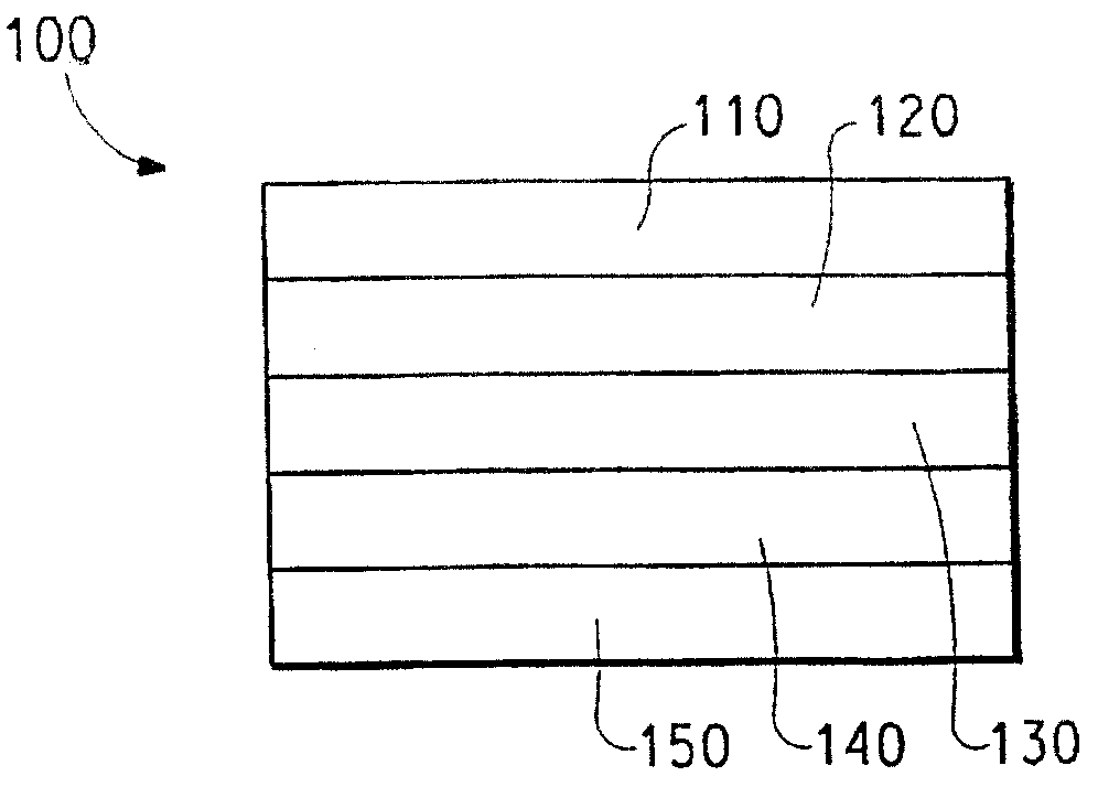
图1所示为含有本发明缓冲层的电子器件的截面图。Fig. 1 shows a cross-sectional view of an electronic device including a buffer layer of the present invention.
图2所示为含有本发明电极的薄膜场效应晶体管的截面图。Fig. 2 is a cross-sectional view of a thin film field effect transistor including an electrode of the present invention.
发明详述Detailed description of the invention
提供了包含导电有机聚合物和许多纳米微粒的水分散体的组合物。这里所用术语“分散体”是指含有微粒悬浮物的连续介质。本发明中的“连续介质”通常是水性液体,例如水。本发明的纳米微粒可以是无机微粒或有机微粒。这里所用术语“无机微粒”是指基本上不含碳的纳米微粒,而“有机微粒”是指基本上由碳组成的纳米微粒。这里所用术语“纳米微粒”是指粒度小于1000纳米(nm)的微粒。A composition comprising an aqueous dispersion of a conductive organic polymer and a plurality of nanoparticles is provided. The term "dispersion" as used herein means a continuous medium containing a suspension of particulates. The "continuous medium" in the present invention is generally an aqueous liquid, such as water. The nanoparticles of the present invention may be inorganic particles or organic particles. As used herein, the term "inorganic particulate" refers to nanoparticles that are substantially free of carbon, and "organic particulate" refers to nanoparticles that consist essentially of carbon. As used herein, the term "nanoparticles" refers to particles having a particle size of less than 1000 nanometers (nm).
本发明的组合物通常包含连续水相,其中分散有导电有机聚合物。举例来说,可用于本发明的导电有机聚合物包括各种形式的聚苯胺(例如无色翠绿亚胺、翠绿亚胺、苯胺黑等),它们能够形成酸/碱盐,提供聚合物导电性。众所周知,根据氧化程度不同,可以合成不同形式的聚苯胺聚合物。聚苯胺(PAni)一般可以说由含有下式I所示芳胺氮原子和/或下式II所示芳亚胺氮原子的单体单元组成:The compositions of the present invention generally comprise a continuous aqueous phase in which is dispersed the conductive organic polymer. Conductive organic polymers useful in the present invention include, for example, various forms of polyaniline (e.g., leuco emeraldine, emeraldine, nigrosine, etc.), which are capable of forming acid/base salts that impart electrical conductivity to the polymer. . It is well known that different forms of polyaniline polymers can be synthesized depending on the degree of oxidation. Polyaniline (PAni) generally can be said to be made up of monomeric units containing the arylamine nitrogen atom shown in the following formula I and/or the arylimine nitrogen atom shown in the following formula II:
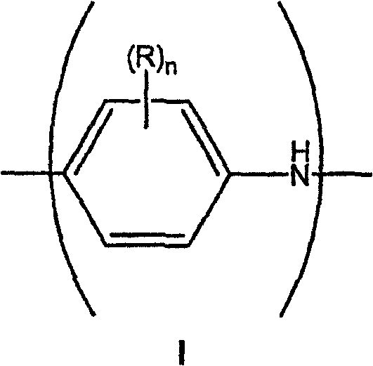
其中,n是0-4之间的整数,Among them, n is an integer between 0-4,
R独立选择,它在每个单元中可相同或不同,选自烷基、烯基、烷氧基、环烷基、环烯基、烷酰基、烷硫基、芳氧基、烷基硫代烷基、烷基芳基、芳烷基、氨基、烷氨基、二烷基氨基、芳基、烷基亚硫酰基、烷氧基烷基、烷基硫酰基、芳硫基、芳基亚硫酰基、烷氧基羰基、芳基硫酰基、羧酸、卤素、氰基,或含有一个或多个磺酸、羧酸、卤素、硝基、氰基或环氧取代基的烷基;或者任何两个R基可一起构成亚烷基或亚烯基链,该链围成3、4、5、6或7元芳环或脂环,该环可任选包含一个或多个二价氮、硫或氧原子。R is independently selected, which may be the same or different in each unit, selected from alkyl, alkenyl, alkoxy, cycloalkyl, cycloalkenyl, alkanoyl, alkylthio, aryloxy, alkylthio Alkyl, alkylaryl, aralkyl, amino, alkylamino, dialkylamino, aryl, alkylsulfinyl, alkoxyalkyl, alkylsulfonyl, arylthio, arylsulfinyl Acyl, alkoxycarbonyl, arylsulfonyl, carboxylic acid, halo, cyano, or alkyl containing one or more sulfonic acid, carboxylic acid, halo, nitro, cyano, or epoxy substituents; or any Two R groups can form an alkylene or alkenylene chain together, and the chain is surrounded by a 3, 4, 5, 6 or 7-membered aromatic ring or alicyclic ring, and the ring can optionally contain one or more divalent nitrogen, sulfur or oxygen atoms.
尽管化学式I和II示出的单体单元是非质子化的,但众所周知,在酸(例如聚(2-丙烯酰氨基-2-甲基-1-丙烷磺酸)(PAAMPSA)、聚(苯乙烯磺酸)(PSS)等)存在下,碱性氮原子将通过质子化形成盐。亚胺氮原子与胺氮原子的相对比例以这样形式增加,具有化学式I的单体单元和具有化学式II的单体单元的比例是2∶1。在此实施方式中,胺氮原子与亚胺氮原子的比例是1∶1。Although the monomer units shown in formulas I and II are non-protonated, it is well known that in acids such as poly(2-acrylamido-2-methyl-1-propanesulfonic acid) (PAAMPSA), poly(styrene In the presence of sulfonic acid) (PSS), etc.), the basic nitrogen atom will form a salt by protonation. The relative ratio of imine nitrogen atoms to amine nitrogen atoms increases in such a way that the ratio of monomeric units of formula I to monomeric units of formula II is 2:1. In this embodiment, the ratio of amine nitrogen atoms to imine nitrogen atoms is 1:1.
在另一种实施方式中,导电有机聚合物是聚(二氧噻吩)。用于本发明的聚(二氧噻吩)具有下式III:In another embodiment, the conductive organic polymer is poly(dioxythiophene). The poly(dioxythiophene)s useful in the present invention have the following formula III:
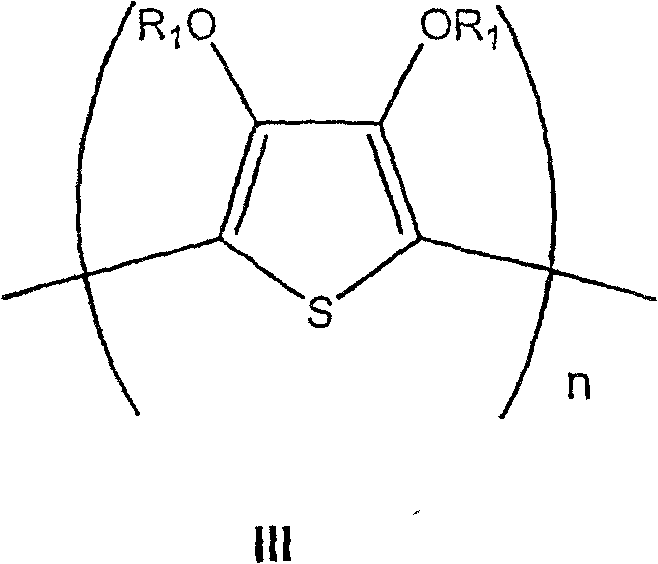
其中:in:
R1和R1’各自独立选自氢和含有1-4个碳原子的烷基,R 1 and R 1 ' are each independently selected from hydrogen and alkyl groups containing 1-4 carbon atoms,
或者R1和R1’一起形成含有1-4个碳原子的亚烷基链,可任选为含有1-12个碳原子的烷基或芳基或1,2-环亚己基所取代,Or R 1 and R 1 ' together form an alkylene chain containing 1-4 carbon atoms, which may be optionally substituted by an alkyl or aryl group or 1,2-cyclohexylene group containing 1-12 carbon atoms,
n约大于9。n is about greater than 9.
用于本发明组合物和方法的导电有机聚合物一般通过在含有聚酸(例如PAMMPSA、PSS等)水溶液中相应单体的氧化聚合反应制备。氧化聚合反应用过硫酸铵、过硫酸钠等氧化剂进行。因此,举例来说,当苯胺在PAAMPSA存在下发生氧化聚合时,形成导电的酸/碱盐PAni/PAAMPSA。当亚乙基二氧噻吩(EDT)在PSS存在下发生氧化聚合时,形成导电的酸/碱盐聚(亚乙基二氧噻吩)(PEDT)/PSS。The conductive organic polymers useful in the compositions and methods of the present invention are generally prepared by oxidative polymerization of the corresponding monomers in aqueous solutions containing polyacids (eg, PAMMPSA, PSS, etc.). Oxidative polymerization is carried out with oxidizing agents such as ammonium persulfate and sodium persulfate. Thus, for example, when aniline is oxidatively polymerized in the presence of PAAMPSA, the conductive acid/base salt PAni/PAAMPSA is formed. When ethylenedioxythiophene (EDT) undergoes oxidative polymerization in the presence of PSS, a conductive acid/base salt poly(ethylenedioxythiophene) (PEDT)/PSS is formed.
水溶液还可包含聚合反应催化剂,如硫酸铁、氯化铁等。聚合反应通常在低温下进行,例如在-10℃至30℃之间。聚合反应完成后,可任选用对所得聚合物的非溶剂,例如丙酮等将聚合物从水分散体中沉淀出来,由此分离聚合物。导电有机聚合物分离后,可对该材料进行精炼,得到粒度约小于1000nm的聚合物微粒。在一种实施方式中,聚合物微粒的粒度约小于500nm。在另一种实施方式中,聚合物微粒约小于50nm。接着,将分离出来的导电有机聚合物微粒要么直接与纳米微粒水分散体直接合并,要么先重新分散在水中,然后再与纳米微粒的水分散体合并。The aqueous solution may also contain polymerization catalysts such as ferric sulfate, ferric chloride, and the like. Polymerization is usually carried out at low temperature, for example between -10°C and 30°C. After completion of the polymerization reaction, the polymer can be isolated by precipitating the polymer from the aqueous dispersion, optionally using a non-solvent for the resulting polymer, such as acetone or the like. After the conductive organic polymer is isolated, the material can be refined to obtain polymer particles with a particle size of less than about 1000 nm. In one embodiment, the polymeric microparticles have a particle size of less than about 500 nm. In another embodiment, the polymeric particles are less than about 50 nm. Next, the isolated conductive organic polymer particles are either directly combined with the aqueous nanoparticle dispersion, or first redispersed in water and then combined with the aqueous nanoparticle dispersion.
在本发明方法的另一种实施方式中,氧化聚合反应在纳米微粒存在下进行,由此产生水分散体,而无需分离导电有机聚合物。例如,可在含苯胺单体的水溶液中加入纳米微粒,从而形成分散体。接着可加入氧化剂,使单体在纳米微粒存在下发生聚合。本发明的此实施方式从经济角度看非常有吸引力,因为它通过“单锅”合成形成了本发明的水分散体。用上述任意一种方法制备的本发明水分散体具有这样一个优点,它容易过滤(例如)通过Millex 0.45μm HV滤器。因此,本发明水分散体很容易形成连续光滑膜。In another embodiment of the method according to the invention, the oxidative polymerization is carried out in the presence of nanoparticles, whereby an aqueous dispersion is produced without isolating the conductive organic polymer. For example, nanoparticles can be added to an aqueous solution containing aniline monomer to form a dispersion. An oxidizing agent can then be added to polymerize the monomer in the presence of the nanoparticles. This embodiment of the invention is very attractive from an economic point of view because it forms the aqueous dispersion of the invention by a "one-pot" synthesis. Aqueous dispersions of the invention prepared by any of the methods described above have the advantage that they are readily filtered, for example, through a Millex 0.45 μm HV filter. Therefore, the aqueous dispersion of the present invention readily forms a continuous smooth film.
在发生氧化聚合反应之前,可任选在水溶液中加入有机添加剂,如位阻稳定剂。这些添加剂有助于形成含有纳米微粒的导电有机聚合物。举例来说,有机添加剂包括聚丙烯酰胺、聚乙烯醇、聚(2-乙烯基吡啶)、聚(乙酸乙烯酯)、聚(乙烯甲基醚)、聚(乙烯吡咯烷酮)、聚(乙烯丁缩醛)等。Organic additives, such as steric stabilizers, may optionally be added to the aqueous solution before the oxidative polymerization takes place. These additives help to form conductive organic polymers containing nanoparticles. Organic additives include, for example, polyacrylamide, polyvinyl alcohol, poly(2-vinylpyridine), poly(vinyl acetate), poly(vinyl methyl ether), poly(vinylpyrrolidone), poly(vinyl butyral aldehyde), etc.
用于本发明的纳米微粒可以是无机微粒或有机微粒。用于本发明的无机纳米微粒包括氧化铝、氧化硅、金属纳米微粒、半导性金属氧化物等。在一种实施方式中,半导电性金属氧化物可选自混合价金属氧化物,如锑酸锌等。在另一种实施方式中,金属纳米微粒是纳米钼。用于本发明的有机纳米微粒包括胶体磺酸(如全氟亚乙基磺酸酯等)、聚丙烯酸酯、聚磷酸酯、碳纳米管等。The nanoparticles used in the present invention may be inorganic particles or organic particles. Inorganic nanoparticles used in the present invention include alumina, silica, metal nanoparticles, semiconductive metal oxides, and the like. In one embodiment, the semiconductive metal oxide can be selected from mixed valence metal oxides, such as zinc antimonate and the like. In another embodiment, the metal nanoparticles are nanomolybdenum. Organic nanoparticles used in the present invention include colloidal sulfonic acid (such as perfluoroethylene sulfonate, etc.), polyacrylate, polyphosphate, carbon nanotubes, and the like.
用于本发明的纳米微粒可具有各种形状和尺寸。在一种实施方式中,纳米微粒基本上是球形的。在另一种实施方式中,纳米微粒基本上是长形的,如金属纳米线。用于本发明的纳米微粒的平均粒径通常约小于500nm。在另一种实施方式中,纳米微粒的平均粒径约小于100nm。在另一种实施方式中,纳米微粒的平均粒径约小于50nm。在另一种实施方式中,长形纳米微粒的长径比大于1-100。长径比定义为微粒宽度与微粒长度之比。对于长形微粒,“粒径”是指微粒宽度。在另一种实施方式中,纳米微粒具有不规则几何形状。对于形状不规则的微粒,“粒度”是指微粒能通过的最小网孔的尺寸。本发明的另一种实施方式提供了由含有导电有机聚合物和纳米微粒的水分散体铸塑而成的缓冲层。导电聚合物和纳米微粒均易分散于水中。因此,可通过铸塑含有导电聚合物和纳米微粒的水分散体来制备连续光滑膜。与组成相同但不含无机纳米微粒的缓冲层相比,本发明缓冲层的电导率下降了。电阻率与电导率成反比。因此,这里所用词汇“高电阻”与“低电导”用来描述缓冲层时,可以互换使用。这里所用词汇“高电阻”和“低电导”各自指电导率小于市售缓冲层的电导,即约小于1.0×10⁻³S/cm。在另一种实施方式中,电导率宜小于1.0×10-5S/cm。电阻率和电导率的值一般分别以欧姆-厘米(Ω-cm)和西门子/厘米(S/cm)报道。这里一般报告电导率值(以S/cm为单位),而不报告电阻率值。Nanoparticles useful in the present invention can be of various shapes and sizes. In one embodiment, the nanoparticles are substantially spherical. In another embodiment, the nanoparticles are substantially elongated, such as metal nanowires. The average particle size of the nanoparticles used in the present invention is generally less than about 500 nm. In another embodiment, the nanoparticles have an average particle size of less than about 100 nm. In another embodiment, the nanoparticles have an average particle size of less than about 50 nm. In another embodiment, the elongated nanoparticles have an aspect ratio greater than 1-100. The aspect ratio is defined as the ratio of particle width to particle length. For elongated particles, "particle size" refers to the width of the particle. In another embodiment, the nanoparticles have an irregular geometry. For irregularly shaped particles, "particle size" refers to the smallest mesh size through which the particles can pass. Another embodiment of the present invention provides a buffer layer cast from an aqueous dispersion comprising a conductive organic polymer and nanoparticles. Both conductive polymers and nanoparticles are easily dispersed in water. Thus, continuous smooth films can be prepared by casting aqueous dispersions containing conductive polymers and nanoparticles. Compared with a buffer layer of the same composition but without inorganic nanoparticles, the conductivity of the buffer layer of the present invention is reduced. Resistivity is inversely proportional to conductivity. Therefore, the terms "high resistance" and "low conductance" used herein can be used interchangeably when used to describe the buffer layer. The terms "high resistance" and "low conductance" as used herein each refer to a conductivity less than that of a commercially available buffer layer, ie less than about 1.0 x 10 -3 S/cm. In another embodiment, the conductivity is preferably less than 1.0×10 −5 S/cm. Values for resistivity and conductivity are generally reported in ohms-centimeter (Ω-cm) and Siemens/centimeter (S/cm), respectively. Conductivity values (in S/cm) are generally reported here, and resistivity values are not reported.
本发明的另一种实施方式提供了两个电接触层之间含有至少一个电致发光层(通常为半导体共轭聚合物)的电子器件,其中器件的至少一个层包含本发明的缓冲层。如图1所示,典型的器件包含阳极层110、缓冲层120、电致发光层130和阴极层150。靠近阴极层150的是任选电子注射/输送层140。在缓冲层120和阴极层150(或任选电子注射/输送层140)之间是电致发光层130。Another embodiment of the invention provides an electronic device comprising at least one electroluminescent layer, typically a semiconducting conjugated polymer, between two electrical contact layers, wherein at least one layer of the device comprises a buffer layer of the invention. As shown in FIG. 1 , a typical device includes an
所述器件包含靠近阳极层110或阴极层150的载体或基底(未示出)。载体多数情况下靠近阳极层110。载体可以是弹性的或刚性的,可以是有机的或无机的。一般,玻璃或弹性有机膜可以用作载体。阳极层110是比阴极层150更有效注射空穴的电极。阳极可以包含含有金属、混合金属、合金、金属氧化物或混合氧化物的材料。合适的材料包括第2族元素(即Be、Mg、Ca、Sr、Ba、Ra)、第11族元素、第4~6族元素和第8~10族过渡元素的混合氧化物。如果阳极层110需要发光,则可用第12~14族元素的混合氧化物,如氧化锡铟。这里所用词汇“混合氧化物”是指含有两种或多种不同阳离子的氧化物,所述阳离子选自第2族元素或第12、13或14族元素。用于阳极层110的材料的某些非限制性具体实例包括氧化锡铟(ITO)、氧化锡铝、金、银、铜和镍。阳极还可包含有机材料,如聚苯胺或聚噻吩。The device includes a carrier or substrate (not shown) adjacent to the
阳极层110可通过化学或物理沉积工艺或旋铸工艺形成。化学气相沉积可以等离子体促进化学气相沉积(PECVD)或金属有机化学气相沉积(MOCVD)的形式进行。物理气相沉积包括所有形式的溅射(包括离子束溅射)以及电子束蒸镀和电阻蒸镀。物理气相沉积的具体形式包括RF磁电管溅射和感应-耦合等离子体物理气相沉积(IMP-PVD)。这些沉积技术在半导体制造领域是广为人知的。The
阳极层110通常在平版印刷操作中成图。所成图案可根据需要变化。阳极层可以这样形成图案,例如,施加第一电接触层材料之前,在第一弹性复合屏蔽结构上放置成图掩模或蚀刻剂。或者,阳极层也可以用作整体层(亦称掩蔽沉积层),然后用如成图蚀刻剂层和湿化学或干蚀刻技术等形成图案。也可以采用本领域熟知的其他成图工艺。如果电子器件排布成列,则阳极层110一般形成基本上平行的条,它们的长度向基本上相同的方向延伸。
缓冲层120通常用本领域技术人员熟悉的各种技术铸塑到基底上。举例来说,常用的铸塑技术包括溶液铸塑、滴铸、幕涂铸塑、旋涂、丝网印刷、喷墨打印等。或者,缓冲层可以用这些技术,如喷墨打印技术成图。
电致发光(EL)层130通常是共轭聚合物,如聚(对亚苯基亚乙烯基)或聚芴。具体材料可根据具体应用、运行时所用电压或其他因素进行选择。含有电致发光有机材料的EL层130可用任何常规技术,包括旋涂、铸塑和印刷技术从溶液中施涂。EL有机材料可用气相沉积工艺直接施用,具体取决于材料的性质。在另一种实施方式中,可施用EL聚合物前体,然后将其转化为聚合物,通常要用到热量或其他外部能源(例如可见光或UV辐射)。Electroluminescent (EL)
任选层140同时具有两个作用,一个是帮助电子注射/输送,另一个是作为约束层,防止猝灭层界面上的反应。更具体地说,层140可促进电子迁移,减少层130和150直接接触时发生猝灭反应的可能。用于任选层140的材料的例子包括金属螯合的oxinoid化合物(例如Alq3等);菲洛啉基化合物(例如2,9-二甲基-4,7-二苯基-1,10-菲洛啉)(DDPA),4,7-二苯基-1,10-菲洛啉(DPA)等);唑类化合物(例如2-(4-联苯基)-5-(4-叔丁基苯基)-1,3,4-噁二唑(PBD等),3-(4-联苯基)-4-苯基-5-(4-叔丁基苯基)-1,2,4-三唑(TAZ等));其他类似化合物;或者它们中的任何一种或多种组合。或者,任选层140可以是无机层,包含BaO、LiF、Li2O等。The
阴极层150是能够特别有效地注射电子或负电荷载体的电极。阴极层150可以是功函小于第一电接触层(在这里是阳极层110)的任何金属或非金属。这里所用术语“功函较小”是指该材料的功函不大于约4.4eV。这里所用“功函较高”是指该材料的功函至少约4.4eV。The
用于阴极层的材料可选自第1族的碱金属(例如Li、Na、K、Rb、Cs)、第2族金属(例如Mg、Ca、Ba等)、第12族金属、镧系元素(例如Ce、Sm、Eu等)和锕系元素(例如Th、U等)。也可以用铝、铟、铱等材料,包括它们的组合。用于阴极层150的材料的具体但非限制性例子包括钡、锂、铈、铯、铕、铷、钇、镁和钐。The material used for the cathode layer may be selected from group 1 alkali metals (e.g. Li, Na, K, Rb, Cs), group 2 metals (e.g. Mg, Ca, Ba, etc.), group 12 metals, lanthanides (such as Ce, Sm, Eu, etc.) and actinides (such as Th, U, etc.). Aluminum, indium, iridium, etc. materials, including combinations thereof, can also be used. Specific but non-limiting examples of materials for
阴极层150通常用化学或物理气相沉积工艺形成。一般地,阴极层可按照上面讨论阳极层110时所用方法成图。如果电子器件排布成列,则阴极层150可形成基本上平行的条,它们的长度方向基本上朝向同一个方向,且基本上垂直于阳极层条的长度方向。称作像素的电子元件形成于交叉点(平视或俯视时,阳极层条与阴极层条交叉的位置)。
在其他实施方式中,有机电子器件中还可存在其他层。例如,缓冲层120和EL层130之间的层(未示出)可促进正电荷的输送、层间带隙匹配,作为保护层等。类似地,EL层130与阴极层150之间的其他层(未示出)可促进负电荷输送、层间带隙匹配,作为保护层等。可以采用本领域熟知的层。此外,任何上述层可由两个或多个层制备。或者,可对无机阳极层110、缓冲层120、EL层130和阴极层150中的某些或全部层进行表面处理,以提高电化载体的输送效率。每个组分层所用材料的选择可在均衡考虑所生产器件的效率、生产成本、生产工艺的复杂程度或其他可能因素之后决定。In other embodiments, other layers may also be present in the organic electronic device. For example, a layer (not shown) between the
根据电子器件的目标用途,EL层130可以是受信号激发的发光层(例如在发光二极管中),或者响应辐射能并发出信号的材料层,可以施加电压或不施加电压(如检测器或伏打电池)。对辐射能有响应的电子器件的例子可选自光导电池、光电导管、光控开关、光电晶体管和光电管,以及光伏打电池。阅读本说明书后,有经验的技术人员将能够选择适合特定应用的材料。发光材料可分散在另一种材料的基体中,可以加入添加剂,也可不加添加剂,但宜单独形成层。EL层130的厚度通常约在50-500nm之间。Depending on the intended use of the electronic device, the
在有机发光二极管(OLED)中,分别从阴极层150和阳极层110注入到EL层130的电子和空穴,在聚合物中形成带负电和带正电的极化子。这些极化子在外加电场作用下发生迁移,形成带有相反电荷的极化激发子,然后进行辐射复合。对器件阳极和阴极之间施加足够的电势差,通常约小于12伏,在许多情况下不大于约5伏。实际电势差取决于器件在较大电子组件中的应用。在许多实施方式中,阳极层110在电子器件的操作中偏置到正电压,而阴极层150基本上为接地电势或0电势。电池或其他电源可电连接到电子器件上,作为电路的一部分,但在图1中没有示出。In an organic light emitting diode (OLED), electrons and holes respectively injected from the
本发明还提供了薄膜场效应晶体管电极。在薄膜场效应晶体管中,介电聚合物或介电氧化物薄膜在一面配有栅极,而另一面配有源极。在漏极和源极之间沉积有机半导体膜。有机半导电聚合物膜一般用芳香溶剂如甲苯,或氯化有机溶剂如氯仿从有机溶液中铸塑而成。为适合电极应用,导电聚合物和用来分散或溶解导电聚合物的液体必须与半导电聚合物和半导电聚合物用的溶剂相容,以避免导电聚合物或半导电聚合物的再溶解。用导电聚合物制备的薄膜场效应晶体管电极的电导率大于10-3S/cm。但是,只用聚合酸制备的导电聚合物的电导率约为~10-3S/cm或更低。为提高导电聚合物的电导率,同时又不会损害其可加工性(如铸塑、旋涂等),需要强导电添加剂。因此,本发明的另一种实施方式提供了薄膜场效应晶体管电极。本发明电极从含有导电聚合物和纳米微粒的水分散体铸塑而成。在此实施方式中,纳米微粒通常是碳纳米管、金属纳米微粒或金属纳米线,所得电极的电导率约大于10-3S/cm。在另一种实施方式中,导电聚合物是聚苯胺/聚合酸,聚二氧亚烷基噻吩/聚合酸等。The invention also provides the thin film field effect transistor electrode. In thin film field effect transistors, a dielectric polymer or dielectric oxide film is provided with a gate on one side and a source on the other. An organic semiconductor film is deposited between the drain and source. Organic semiconducting polymer films are typically cast from organic solutions using aromatic solvents such as toluene, or chlorinated organic solvents such as chloroform. To be suitable for electrode applications, the conductive polymer and the liquid used to disperse or dissolve the conductive polymer must be compatible with the semiconductive polymer and the solvent used for the semiconductive polymer to avoid redissolution of the conductive polymer or the semiconductive polymer. The conductivity of the thin film field effect transistor electrode prepared by conducting polymer is greater than 10 -3 S/cm. However, conductive polymers prepared using only polymeric acid have a conductivity of about ~10 −3 S/cm or lower. In order to increase the conductivity of conductive polymers without compromising their processability (e.g. casting, spin coating, etc.), strongly conductive additives are required. Accordingly, another embodiment of the present invention provides a thin film field effect transistor electrode. The electrodes of the present invention are cast from aqueous dispersions containing conductive polymers and nanoparticles. In this embodiment, the nanoparticles are typically carbon nanotubes, metal nanoparticles or metal nanowires, and the conductivity of the resulting electrode is greater than about 10 −3 S/cm. In another embodiment, the conductive polymer is polyaniline/polymeric acid, polydioxyalkylenethiophene/polymeric acid, or the like.
本发明还提供了含有本发明电极的薄膜场效应晶体管。图2所示薄膜场效应晶体管通常按以下方法制备。介电聚合物或介电氧化物薄膜210的一面有栅极220,而另一面分别有漏极和源极230和240。漏极和源极之间沉积了有机半导电膜250。本发明含有纳米线或碳纳米管的水分散体在栅极、漏极和源极上可得到理想的应用,因为它们与溶液薄膜沉积中的有机介电聚合物和半导电聚合物相容。The present invention also provides a thin film field effect transistor comprising the electrode of the present invention. The thin film field effect transistor shown in Fig. 2 is generally prepared by the following method. Dielectric polymer or
本发明的另一种实施方式提供了降低从水分散体铸塑在基底上的导电有机聚合物膜电导率的方法,使电导率小于约1×10⁻⁵S/cm。举例来说,这种方法可通过在导电聚合物的水分散体中加入许多纳米微粒来进行。令人意外的发现是,即使在这里所述导电有机聚合物膜中加入半导电无机纳米微粒,也能降低聚合物膜的电导率。在一种实施方式中,导电有机聚合物膜可用作电致发光器件的缓冲层。在另一种实施方式中,导电聚合物膜是PAni/PAAMPSA。Another embodiment of the present invention provides a method of reducing the conductivity of a conductive organic polymer film cast on a substrate from an aqueous dispersion to a conductivity of less than about 1 x 10 -5 S/cm. For example, this method can be carried out by adding many nanoparticles to the aqueous dispersion of the conductive polymer. It was surprisingly found that even the incorporation of semiconducting inorganic nanoparticles into the conductive organic polymer films described herein reduces the conductivity of the polymer films. In one embodiment, a conductive organic polymer film can be used as a buffer layer for an electroluminescent device. In another embodiment, the conductive polymer film is PAni/PAAMPSA.
本发明的另一种实施方式提供了制造更厚缓冲层的方法。举例来说,这种方法可这样进行,即在导电有机聚合物的水分散体中加入许多纳米微粒,然后将所述水分散体铸塑到基底上,形成缓冲层。在导电聚合物的水分散体中加入纳米微粒后,得到的水分散体的粘度提高。提高粘度后,可更好地控制由水溶液铸塑而成的层的厚度。控制缓冲层的厚度是有利的,因为功能正常的缓冲层的合适厚度在一定程度上取决于沉积缓冲层的金属导电层的表面粗糙度。Another embodiment of the invention provides a method of making a thicker buffer layer. For example, this method can be carried out by adding a plurality of nanoparticles to an aqueous dispersion of a conductive organic polymer and then casting the aqueous dispersion onto a substrate to form a buffer layer. After adding nanoparticles to an aqueous dispersion of conductive polymer, the viscosity of the resulting aqueous dispersion increases. Increased viscosity provides better control over the thickness of layers cast from aqueous solutions. Controlling the thickness of the buffer layer is advantageous because the appropriate thickness for a properly functioning buffer layer depends in part on the surface roughness of the metal conductive layer on which the buffer layer is deposited.
下面将结合以下非限制性实施例对本发明进行更详细的介绍。The present invention will be described in more detail below in conjunction with the following non-limiting examples.
实施例 Example
比较例1Comparative example 1
此比较例说明了PAni/PAAMPSA的制备,及其作为缓冲层的电导率和发光器件性质。This comparative example illustrates the preparation of PAni/PAAMPSA, and its conductivity and light emitting device properties as a buffer layer.
按以下方法合成。将苯胺(4.08g)溶解在150ml含有PAAMPSA(6.35g,购自Sigma-Aldrich Corp.,St.Louis,MO,USA的PAAMPSA)的水溶液中,形成15wt%水溶液;PAAMPSA的重均分子量是2,000,000。将含有苯胺和PAAMPSA的水溶液装入500ml四颈圆底烧瓶中,用冰/水浴冷却到约4℃。用磁力搅拌器连续搅拌溶液。在冷却的苯胺/PAAMPSA水溶液中,以恒定速率在1小时时间内加入100ml含有4.235g PAAMPSA和2.36g过硫酸铵的水溶液。聚合反应进行198分钟。Synthesized as follows. Aniline (4.08 g) was dissolved in 150 ml of an aqueous solution containing PAAMPSA (6.35 g, PAAMPSA purchased from Sigma-Aldrich Corp., St. Louis, MO, USA) to form a 15 wt% aqueous solution; the weight average molecular weight of PAAMPSA was 2,000,000. The aqueous solution containing aniline and PAAMPSA was charged into a 500ml four-neck round bottom flask and cooled to about 4°C with an ice/water bath. The solution was stirred continuously with a magnetic stirrer. To the cooled aniline/PAAMPSA aqueous solution, 100 ml of an aqueous solution containing 4.235 g PAAMPSA and 2.36 g ammonium persulfate was added at a constant rate over a period of 1 hour. Polymerization was carried out for 198 minutes.
然后将反应混合物倒入两个离心瓶中,在15℃下以8000rpm的速度离心30分钟。离心之后,将上清液缓慢倒入丙酮,沉淀出聚合物产物。沉淀之后,用丙酮反复冲洗固体聚合物,过滤,在真空炉(约18Hg.,通N2,室温)中干燥过夜,产量为7.03g。The reaction mixture was then poured into two centrifuge bottles and centrifuged at 8000 rpm for 30 minutes at 15°C. After centrifugation, the supernatant was slowly poured into acetone to precipitate the polymer product. After precipitation, the solid polymer was rinsed repeatedly with acetone, filtered, and dried overnight in a vacuum oven (ca. 18 Hg., N2 , room temperature), yielding 7.03 g.
将上面制备的PAni/PAAMPSA(1.21g)分散在39.12g去离子水中,固体占水溶液的3.0wt%。测定分散体的电导率和发光性质。将商购的含100-150nm厚的ITO层的氧化锡铟(ITO)/玻璃板切成30mm×30mm的样品30。接着用氧等离子体蚀刻ITO层。将玻璃基底上用来测定电导率的ITO蚀刻成一系列平行ITO线,用作电极。将基底上要制成LED用于发光测定的ITO蚀刻成15mm×20mm的ITO层,作为阳极。然后以1200rpm的旋转速度将水分散体旋涂每块ITO/玻璃基底上。所得PAni/PAAMPSA层厚约137nm。The PAni/PAAMPSA prepared above (1.21 g) was dispersed in 39.12 g of deionized water, the solids represented 3.0 wt% of the aqueous solution. The electrical conductivity and luminescence properties of the dispersions were determined. A commercially available indium tin oxide (ITO)/glass plate containing a 100-150 nm thick ITO layer was cut into 30 mm x 30 mm samples 30 . The ITO layer is then etched with oxygen plasma. The ITO used to measure the conductivity on the glass substrate was etched into a series of parallel ITO lines, which were used as electrodes. The ITO on the substrate to be made into an LED for luminescence measurement was etched into an ITO layer of 15 mm×20 mm, which was used as an anode. The aqueous dispersion was then spin-coated onto each ITO/glass substrate at a spin speed of 1200 rpm. The resulting PAni/PAAMPSA layer was about 137 nm thick.
用于测定粘度的样品按如下方法制备:0.0989g PAni/PAAMPSA与9.9081g去离子水混合,PAni/PAAMPSA占分散体的0.99wt%。对混合物磁力搅拌过夜。应当指出,与本发明实施例4相比,尽管旋涂速度低(1200rpm对6000rpm),本实施例的涂层厚度小于实施例4(137nm对300nm)。比较显示,所得分散体的粘度小于实施例4的分散体粘度。Samples for viscosity determination were prepared as follows: 0.0989 g PAni/PAAMPSA was mixed with 9.9081 g deionized water, PAni/PAAMPSA accounted for 0.99 wt% of the dispersion. The mixture was stirred magnetically overnight. It should be noted that compared with Example 4 of the present invention, the coating thickness of this example is smaller than that of Example 4 (137nm vs. 300nm) despite the lower spin coating speed (1200rpm vs. 6000rpm). The comparison shows that the viscosity of the resulting dispersion is less than that of Example 4.
涂有PAni/PAAMPSA的ITO/玻璃基底在90℃氮气中干燥30分钟,然后测定电导率。电导率是通过测定两个电极间的电阻来确定的,然后根据电阻、导电层厚度和用来测定电阻的两个电极间的距离计算得到3.6×10-5S/cm。电导率示于表1。The ITO/glass substrates coated with PAni/PAAMPSA were dried at 90°C in nitrogen for 30 minutes, and then the electrical conductivity was measured. Conductivity was determined by measuring the resistance between two electrodes, and then calculated to be 3.6 x 10 -5 S/cm from the resistance, the thickness of the conductive layer and the distance between the two electrodes used to measure the resistance. The electrical conductivity is shown in Table 1.
对于发光测定,当PAni/PAAMPSA层加入到发光二极管(LED)中时,其顶部涂有超黄发光聚(取代的亚苯基亚乙烯基)(PDY 131,购自Covion Company,Frankfurt,Germay),作为活性电致发光(EL)层。EL层的厚度约为70nm。所有膜厚用TENCOR 500 Surface Profiler测定。对于阴极,在1.3×10⁻⁴Pa的压力下将Ba和Al层气相沉积到EL层上。Ba层的最终厚度为3nm;Ba层顶部的Al层厚度为300nm。LED器件的性能按如下方法测定。用Keithley InstrumentInc.(Cleveland,OH)生产的Keithley 236源-测量单元和带有校准硅光二极管的S370 Optometer(UDT Sensor,Inc.,Hawthorne,CA)测定电流-外加电压、发光亮度-外加电压和发光效率(坎德拉/安培-cd/A)。室温下给5个LED施加电流,电流密度为8.3mA/cm2。得到这种电流密度的平均电压为4.2伏,平均发光效率和发光亮度分别为8.3cd/A和115cd/m2,总结于表1。表1还列出了器件在80℃下,电流密度为3.3mA/cm2时的半寿期为12小时。For luminescence assays, when the PAni/PAAMPSA layer was added to a light-emitting diode (LED), it was top-coated with ultra-yellow luminescent poly(substituted phenylenevinylene) (PDY 131, purchased from Covion Company, Frankfurt, Germany) , as an active electroluminescent (EL) layer. The thickness of the EL layer is about 70 nm. All film thicknesses were measured with a TENCOR 500 Surface Profiler. For the cathode, Ba and Al layers were vapor-deposited on the EL layer at a pressure of 1.3 x 10 -4 Pa. The final thickness of the Ba layer was 3 nm; the thickness of the Al layer on top of the Ba layer was 300 nm. The properties of the LED devices were measured as follows. A Keithley 236 source-measure unit produced by Keithley Instrument Inc. (Cleveland, OH) and a S370 Optometer (UDT Sensor, Inc., Hawthorne, CA) with a calibrated silicon photodiode were used to measure current-applied voltage, luminance-applied voltage and Luminous efficiency (candela/ampere-cd/A). A current was applied to 5 LEDs at room temperature with a current density of 8.3 mA/cm 2 . The average voltage to obtain this current density was 4.2 volts, and the average luminous efficiency and luminous brightness were 8.3 cd/A and 115 cd/m 2 , respectively, summarized in Table 1. Table 1 also lists the half-life of the device as 12 hours at a current density of 3.3mA/ cm2 at 80°C.
实施例1Example 1
本实施例说明了如何用氧化硅纳米微粒制备PAni/PAAMPSA水分散体,及其作为缓冲层的电导率和发光性质。This example illustrates how to prepare a PAni/PAAMPSA aqueous dispersion with silica nanoparticles, and its conductivity and luminescent properties as a buffer layer.
按比较例1所述方法制备的PAni/PAAMPSA(0.63g)与0.75gSnowtex-

用和比较例1所述相同的方法测定分散体的电导率和发光性质。如表1所示结果,由实施例1的分散体铸塑而成的缓冲层的电导率比比较例1低(8.2×10⁻⁷S/cm对3.6×10-5S/cm),半寿期比比较例1长(29小时对12小时)。此实施例表明纳米微粒在降低电导率和提高器件半寿期上的效应。The electrical conductivity and luminescent properties of the dispersion were measured in the same manner as described in Comparative Example 1. As shown in Table 1, the conductivity of the buffer layer cast from the dispersion of Example 1 is lower than that of Comparative Example 1 (8.2×10 -7 S/cm vs. 3.6×10 -5 S/cm), half The lifetime is longer than Comparative Example 1 (29 hours vs. 12 hours). This example demonstrates the effect of nanoparticles in reducing electrical conductivity and increasing device half-life.
实施例2Example 2
本实施例说明了如何用胶体氧化硅制备PAni/PAAMPSA水分散体,及其作为缓冲层的电导率和发光性质。This example illustrates how to prepare a PAni/PAAMPSA aqueous dispersion with colloidal silica, and its conductivity and luminescent properties as a buffer layer.
按比较例1所述方法制备的PAni/PAAMPSA(0.61g)与Snowtex-(0.75g,Nissan Chemical Industries,Ltd.,Tokyo,Japan)混合,Snowtex-

用和比较例1所述相同的方法测定分散体的电导率和发光性质。如表1所示结果,由实施例2的分散体铸塑而成的缓冲层的电导率比比较例1低(7.6×10⁻⁷S/cm对3.6×10-5S/cm),半寿期比比较例1长(30小时对12小时)。此实施例表明纳米微粒在降低电导率和提高器件半寿期上的效应。The electrical conductivity and luminescent properties of the dispersion were measured in the same manner as described in Comparative Example 1. As shown in Table 1, the conductivity of the buffer layer cast from the dispersion of Example 2 is lower than that of Comparative Example 1 (7.6×10 -7 S/cm vs. 3.6×10 -5 S/cm), half The lifetime is longer than Comparative Example 1 (30 hours vs. 12 hours). This example demonstrates the effect of nanoparticles in reducing electrical conductivity and increasing device half-life.
实施例3Example 3
此实施例说明了如何用半导电性氧化物制备PAni/PAAMPSA水分散体,及其作为缓冲层的电导率和发光性质。This example illustrates how to prepare an aqueous dispersion of PAni/PAAMPSA with a semiconducting oxide, and its conductivity and luminescent properties as a buffer layer.
按比较例1所述方法制备的PAni/PAAMPSA(0.90g)与CelnaxCX-
用和比较例1所述相同的方法测定分散体的电导率和发光性质。如表1所示结果,由实施例3的分散体铸塑而成的缓冲层的电导率比比较例1低(8.3×10⁻⁸S/cm对3.6×10-5S/cm),半寿期比比较例1长(61小时对12小时)。此实施例表明纳米微粒在降低电导率和提高器件半寿期上的效应。The electrical conductivity and luminescent properties of the dispersion were measured in the same manner as described in Comparative Example 1. As shown in Table 1, the conductivity of the buffer layer cast from the dispersion of Example 3 is lower than that of Comparative Example 1 (8.3×10 -8 S/cm vs. 3.6×10 -5 S/cm), half The lifetime is longer than Comparative Example 1 (61 hours vs. 12 hours). This example demonstrates the effect of nanoparticles in reducing electrical conductivity and increasing device half-life.
实施例4Example 4
此实施例说明了在SiO2纳米微粒的存在下制备本发明的PAni/PAAMPSA水分散体,及其作为缓冲层的电导率和发光性质。This example illustrates the preparation of an aqueous dispersion of PAni/PAAMPSA according to the invention in the presence of SiO nanoparticles, and their conductivity and luminescent properties as a buffer layer.
在SiO2纳米微粒存在下PAni/PAAMPSA的合成按如下方式进行。将PAAMPSA(36.32g 15wt%水溶液,购自Sigma-Aldrich Corp.,St.Louis,MO,USA)加入到250塑料瓶中。向PAni/PAAMPSA溶液中加入Snowtex-


然后将反应混合物倒入两个离心瓶中,在15℃下以8000rpm的速度离心30分钟。离心之后,将上清液缓慢倒入丙酮,沉淀出聚合物产物。沉淀之后,用丙酮反复冲洗固体聚合物,过滤,在真空炉(约18Hg.,通N2,室温)中干燥过夜,产率为14.19g。应当指出,这里的产率几乎是比较例1的产率的2倍。产率的提高表明SiO2纳米微粒存在于PAni/PAAMPSA内部。The reaction mixture was then poured into two centrifuge bottles and centrifuged at 8000 rpm for 30 minutes at 15°C. After centrifugation, the supernatant was slowly poured into acetone to precipitate the polymer product. After precipitation, the solid polymer was rinsed repeatedly with acetone, filtered, and dried overnight in a vacuum oven (ca. 18 Hg., N2 , room temperature), yield 14.19 g. It should be noted that the yield here is almost double that of Comparative Example 1. The increase in yield indicated the presence of SiO2 nanoparticles inside PAni/PAAMPSA.
将PAni/PAAMPSA/SiO2(1.20g,上面制备的)分散在38.80g去离子水中,固体占水溶液的3.0wt%。如前面实施例所述,将缓冲层铸塑到ITO基底上。对于发光测定,在PAni/PAAMPSA/氧化硅层顶部上涂布超黄发光聚(取代的亚苯基亚乙烯基)(PDY 131,购自Covion Company,Frankfurt,Germay),作为LED器件中的活性电致发光(EL)层。EL层的厚度约为70nm。所有膜厚利用TENCOR500 Surface Profiler测定。对于阴极,在1.3×10⁻⁴Pa的真空下将Ba 和Al层气相沉积到EL层上。Ba层的最终厚度为3nm;Ba层顶部的Al层厚度为300nm。LED器件的性能按如下方法测定。用Keithley Instrument Inc.(Cleveland,OH)制造的Keithley 236源-测量单元和带有校准硅光二极管的S370 Optometer(UDTSensor,Inc.,Hawthorne,CA)测定电流-外加电压、发光亮度-外加电压和发光效率(坎德拉/安培-cd/A)。室温下给5个LED器件的每个器件施加电流,电流密度为8.3mA/cm2。得到这种电流密度的平均电压为4.3伏,平均发光效率和发光亮度分别为5.3cd/A和130cd/m2,总结于表1。表1还列出了器件在80℃下,电流密度为3.3mA/cm2时的半寿期为42小时。应当指出,与比较例1中不含氧化硅的PAni/PAAMPSA相比,尽管厚度是比较例1的2.2倍,本实施例的半寿期仍然提高了4倍,而且发光强度更高(130cd/m2对115cd/m2)。PAni/PAAMPSA/ SiO2 (1.20 g, prepared above) was dispersed in 38.80 g of deionized water, solids represented 3.0 wt% of the aqueous solution. The buffer layer was cast onto the ITO substrate as described in the previous examples. For luminescence measurements, super yellow luminescent poly(substituted phenylenevinylene) (PDY 131, purchased from Covion Company, Frankfurt, Germany) was coated on top of the PAni/PAAMPSA/silica layer as active in LED devices. Electroluminescence (EL) layer. The thickness of the EL layer is about 70 nm. All film thicknesses were measured using a TENCOR500 Surface Profiler. For the cathode, Ba and Al layers were vapor-deposited on the EL layer under a vacuum of 1.3 x 10 -4 Pa. The final thickness of the Ba layer was 3 nm; the thickness of the Al layer on top of the Ba layer was 300 nm. The properties of the LED devices were measured as follows. Current-applied voltage, luminance-applied voltage and Luminous efficiency (candela/ampere-cd/A). A current was applied to each of the 5 LED devices at room temperature with a current density of 8.3 mA/cm 2 . The average voltage to obtain this current density was 4.3 volts, and the average luminous efficiency and luminous brightness were 5.3 cd/A and 130 cd/m 2 , respectively, summarized in Table 1. Table 1 also lists the half-life of the device as 42 hours at a current density of 3.3mA/ cm2 at 80°C. It should be noted that compared with PAni/PAAMPSA without silicon oxide in Comparative Example 1, although the thickness is 2.2 times that of Comparative Example 1, the half-life of this embodiment is still improved by 4 times, and the luminous intensity is higher (130cd/ m 2 vs. 115 cd/m 2 ).
表1Table 1
在PAni/PAAMPSA中加入无机纳米微粒对玻璃基底上Inorganic nanoparticles added to PAni/PAAMPSA on glass substrate
OLED发光性质的影响Effect of OLED Luminescence Properties
如表2所示,实施例4的水分散体在6000rpm的旋转速度下得到300nm的涂层厚度。该涂层厚度比比较例1的厚度高得多(300nm对137nm),虽然其旋涂速度高(6000rpm对1200rpm)。比较显示,用氧化硅纳米微粒聚合的PAni/PAAMPSA比不用氧化硅纳米微粒聚合的PAni/PAAMPSA具有更高的粘度。如表2所示,粘度的增加导致了缓冲层厚度的增加。用于测定粘度的分散体用如下方法制备:0.0999g PAni/PAAMPSA/氧化硅与9.9164g去离子水混合,PAni/PAAMPSA/氧化硅在分散体中占1.00wt%。As shown in Table 2, the aqueous dispersion of Example 4 gave a coating thickness of 300 nm at a rotation speed of 6000 rpm. The coating thickness is much higher than that of Comparative Example 1 (300nm vs. 137nm), despite the high spin-coating speed (6000rpm vs. 1200rpm). The comparison shows that PAni/PAAMPSA polymerized with silica nanoparticles has a higher viscosity than PAni/PAAMPSA polymerized without silica nanoparticles. As shown in Table 2, an increase in viscosity resulted in an increase in buffer layer thickness. The dispersion used to measure the viscosity was prepared as follows: 0.0999g PAni/PAAMPSA/silica was mixed with 9.9164g deionized water, PAni/PAAMPSA/silica accounted for 1.00 wt% of the dispersion.
表2Table 2
PAni/PAAMPSA水分散体的粘度Viscosity of PAni/PAAMPSA aqueous dispersion

实施例5Example 5
本实施例说明了由市售PEDT水分散体在有机溶剂中制备的固体膜的整体性。This example demonstrates the integrity of solid films prepared from commercial PEDT aqueous dispersions in organic solvents.
在此实施例中,在室温和氮气流下,在玻璃烧杯中将市售PEDT水分散体(Baytron-P VP A1 4083,购自H.C.Starck,GmbH,Leverkusen,Germany)干燥成固体膜,其中PEDT水分散体的电导率约为10-3S/cm。干燥膜与薄膜场效应晶体管的生产中用来溶解有机半导电聚合物的普通有机溶剂(如甲苯、氯仿、二氯甲烷等)混合。膜片既没有为有机液体所膨胀,也没有使液体褪色。这个结果清楚地表明,用Baytron-P制备的PEDT膜与半导电聚合物用有机溶剂相容,因而可以用作薄膜场效应晶体管。In this example, a commercially available aqueous PEDT dispersion (Baytron-P VP A1 4083, purchased from HC Starck, GmbH, Leverkusen, Germany) was dried in a glass beaker at room temperature under nitrogen flow to form a solid film in which the PEDT aqueous dispersion The conductivity of the body is about 10 -3 S/cm. The dried film is mixed with common organic solvents (such as toluene, chloroform, dichloromethane, etc.) used to dissolve organic semiconducting polymers in the production of thin film field effect transistors. The diaphragm is neither swollen by the organic liquid nor discolored by the liquid. This result clearly shows that the PEDT film prepared with Baytron-P is compatible with semiconducting polymers with organic solvents and thus can be used as a thin film field effect transistor.
实施例6Example 6
本实施例说明了由PAni/PAAMPSA水分散体在有机溶剂中的水分散体制备的固体膜的整体性。This example demonstrates the integrity of solid films prepared from aqueous dispersions of PAni/PAAMPSA in organic solvents.
在此实施例中,在室温和氮气流下,在玻璃烧杯中将比较例1制备的PAni/PAAMPSA水分散体干燥成固体膜。干燥膜与薄膜场效应晶体管的生产中用来溶解有机半导电聚合物的普通有机溶剂混合(如甲苯、氯仿、二氯甲烷等)混合。膜片既没有为有机液体所膨胀,也没有使液体脱色。这个结果清楚地表明,用PAni/PAAMPSA水分散体制备的PAni/PAAMPSA膜与半导电聚合物用有机溶剂相容,因而可以用作薄膜场效应晶体管。In this example, the PAni/PAAMPSA aqueous dispersion prepared in Comparative Example 1 was dried to a solid film in a glass beaker at room temperature under nitrogen flow. The dried film is mixed with common organic solvents (such as toluene, chloroform, methylene chloride, etc.) used to dissolve organic semiconducting polymers in the production of thin film field effect transistors. The diaphragm was neither swelled by the organic liquid nor discolored the liquid. This result clearly shows that the PAni/PAAMPSA films prepared from aqueous PAni/PAAMPSA dispersions are compatible with organic solvents for semiconducting polymers and thus can be used as thin film field effect transistors.
实施例7Example 7
本实施例说明了含有聚苯胺/聚酸或聚(二氧亚乙基噻吩)/聚酸和强导电纳米微粒的水分散体的制备。This example illustrates the preparation of aqueous dispersions containing polyaniline/polyacid or poly(dioxyethylenethiophene)/polyacid and strongly conductive nanoparticles.
如比较例1所述,由PAni/PAAMPSA水分散体铸塑而成的PAni/PAAMPSA的电导率仅为3.6×10-5S/cm,它不足以用作薄膜场效应晶体管的栅极、漏极和源极。用PAni水分散体,例如Ormecon(Ammersbeck,Germany)或PEDT水分散体,例如Baytron-P曾经得到的最高电导率约为10-3S/cm,对于实际应用来说仍太低。但是,使用本发明含有纳米微粒,如金属纳米线或纳米微粒或纳米碳管的导电聚合物水分散体可极大提高用这些水分散体铸塑而成的电极的电导率。例如,直径为15nm、电导率为1.7×104S/cm的金属钼线可用来提高电导率。直径为8nm、长20μm、电导率为60S/cm的碳纳米管也可用来提高电导率。由于纳米微粒具有高电导率,且微粒在水中有很好的分散性,由导电聚合物和强导电纳米微粒组成的复合水分散体很容易用来制备连续光滑膜,用作薄膜场效应晶体管的漏极、源极或栅极。As described in Comparative Example 1, the conductivity of PAni/PAAMPSA cast from PAni/PAAMPSA aqueous dispersion is only 3.6× 10⁻⁵ S/cm, which is not enough to be used as the gate and drain of thin film field effect transistors. pole and source. The highest conductivity ever obtained with aqueous PAni dispersions such as Ormecon (Ammersbeck, Germany) or PEDT aqueous dispersions such as Baytron-P is about 10 −3 S/cm, which is still too low for practical applications. However, the use of the inventive aqueous conductive polymer dispersions containing nanoparticles, such as metal nanowires or nanoparticles or carbon nanotubes, can greatly increase the conductivity of electrodes cast from these aqueous dispersions. For example, metallic molybdenum wires with a diameter of 15 nm and a conductivity of 1.7×10 4 S/cm can be used to increase the conductivity. Carbon nanotubes with a diameter of 8 nm, a length of 20 μm, and a conductivity of 60 S/cm can also be used to increase the conductivity. Due to the high electrical conductivity of nanoparticles and the good dispersibility of the particles in water, the composite aqueous dispersion composed of conductive polymers and strongly conductive nanoparticles can be easily used to prepare continuous smooth films, which can be used as thin film field effect transistors. Drain, Source or Gate.
虽然已经结合特定的优选实施方式对本发明进行了详细介绍,但应当理解,各种改进和变化形式包括在在所叙述及权利所要求的主旨和范围之内。Although the present invention has been described in detail in conjunction with specific preferred embodiments, it should be understood that various improvements and changes are included within the spirit and scope of the description and claims.
Claims (9)
Applications Claiming Priority (2)
| Application Number | Priority Date | Filing Date | Title |
|---|---|---|---|
| US41311402P | 2002-09-24 | 2002-09-24 | |
| US60/413,114 | 2002-09-24 |
Publications (2)
| Publication Number | Publication Date |
|---|---|
| CN1685031A CN1685031A (en) | 2005-10-19 |
| CN100540628C true CN100540628C (en) | 2009-09-16 |
Family
ID=32043203
Family Applications (1)
| Application Number | Title | Priority Date | Filing Date |
|---|---|---|---|
| CNB038225239A Expired - Lifetime CN100540628C (en) | 2002-09-24 | 2003-09-24 | Conductive organic polymer/nanoparticle compositions and methods of application thereof |
Country Status (9)
| Country | Link |
|---|---|
| US (3) | US20040124504A1 (en) |
| EP (2) | EP2341118A1 (en) |
| JP (2) | JP4464277B2 (en) |
| KR (1) | KR101021749B1 (en) |
| CN (1) | CN100540628C (en) |
| AU (1) | AU2003279011A1 (en) |
| CA (1) | CA2500304A1 (en) |
| TW (1) | TWI302563B (en) |
| WO (1) | WO2004029176A1 (en) |
Families Citing this family (108)
| Publication number | Priority date | Publication date | Assignee | Title |
|---|---|---|---|---|
| US6723299B1 (en) | 2001-05-17 | 2004-04-20 | Zyvex Corporation | System and method for manipulating nanotubes |
| US6905667B1 (en) | 2002-05-02 | 2005-06-14 | Zyvex Corporation | Polymer and method for using the polymer for noncovalently functionalizing nanotubes |
| US20040034177A1 (en) | 2002-05-02 | 2004-02-19 | Jian Chen | Polymer and method for using the polymer for solubilizing nanotubes |
| AU2003275203A1 (en) | 2002-09-24 | 2004-04-19 | E.I. Du Pont De Nemours And Company | Water dispersible polythiophenes made with polymeric acid colloids |
| US7317047B2 (en) * | 2002-09-24 | 2008-01-08 | E.I. Du Pont De Nemours And Company | Electrically conducting organic polymer/nanoparticle composites and methods for use thereof |
| CN100540628C (en) * | 2002-09-24 | 2009-09-16 | E.I.内穆尔杜邦公司 | Conductive organic polymer/nanoparticle compositions and methods of application thereof |
| US7462298B2 (en) * | 2002-09-24 | 2008-12-09 | E.I. Du Pont De Nemours And Company | Water dispersible polyanilines made with polymeric acid colloids for electronics applications |
| KR100704795B1 (en) * | 2002-11-01 | 2007-04-09 | 미츠비시 레이온 가부시키가이샤 | Carbon nanotube-containing compositions, composites having a coating film comprising the same, and methods for producing the same |
| JP3913208B2 (en) * | 2002-11-01 | 2007-05-09 | 三菱レイヨン株式会社 | Carbon nanotube-containing composition, composite having coating film made thereof, and method for producing them |
| JP4394890B2 (en) * | 2003-03-10 | 2010-01-06 | 株式会社Kri | Conductive composition, conductive film, resin composite material |
| US7390438B2 (en) * | 2003-04-22 | 2008-06-24 | E.I. Du Pont De Nemours And Company | Water dispersible substituted polydioxythiophenes made with fluorinated polymeric sulfonic acid colloids |
| CN1777648B (en) * | 2003-04-22 | 2011-06-08 | E.I.内穆尔杜邦公司 | Water-dispersible polythiophenes prepared from polymer acidic colloids |
| KR100827861B1 (en) | 2003-05-22 | 2008-05-07 | 지벡스 퍼포먼스 머티리얼즈, 엘엘씨 | Nanocomposites and methods thereto |
| DE10325102B3 (en) * | 2003-06-03 | 2004-05-27 | Fraunhofer-Gesellschaft zur Förderung der angewandten Forschung e.V. | Rigid chain, conjugated, organic solvent-insoluble polymer dispersion in aqueous and/or organic medium used for producing thin film electronic device e.g. FET, LED or photovoltaic cell, is prepared from solution e.g. in strong acid |
| US7351358B2 (en) | 2004-03-17 | 2008-04-01 | E.I. Du Pont De Nemours And Company | Water dispersible polypyrroles made with polymeric acid colloids for electronics applications |
| US8147962B2 (en) * | 2004-04-13 | 2012-04-03 | E. I. Du Pont De Nemours And Company | Conductive polymer composites |
| KR100632632B1 (en) | 2004-05-28 | 2006-10-12 | 삼성전자주식회사 | Method for preparing a multi-layer of nano-crystals and organic-inorganic hybrid electro-luminescence device using the same |
| KR100736521B1 (en) * | 2004-06-09 | 2007-07-06 | 삼성전자주식회사 | Nano Crystal Electroluminescent Device and Manufacturing Method Thereof |
| KR20060004158A (en) * | 2004-07-08 | 2006-01-12 | 박철용 | Aqueous conductive polymer composition having PitiC properties and its manufacturing method |
| US7296576B2 (en) | 2004-08-18 | 2007-11-20 | Zyvex Performance Materials, Llc | Polymers for enhanced solubility of nanomaterials, compositions and methods therefor |
| JP4534674B2 (en) * | 2004-08-31 | 2010-09-01 | 日産自動車株式会社 | Functional thin film element, method for producing functional thin film element, and article using functional thin film element |
| JP4534673B2 (en) * | 2004-08-31 | 2010-09-01 | 日産自動車株式会社 | Functional thin film element, method for producing functional thin film element, and article using functional thin film element |
| KR101195714B1 (en) | 2004-09-09 | 2012-10-29 | 미츠비시 레이온 가부시키가이샤 | Nanomaterial-containing composition, preparation method thereof and composite using same |
| JP4824971B2 (en) * | 2004-09-09 | 2011-11-30 | 三菱レイヨン株式会社 | Nanomaterial-containing composition, method for producing the same, and composite using the same |
| DE602005003425T2 (en) * | 2004-10-11 | 2008-10-02 | Samsung SDI Co., Ltd., Suwon | Organic electroluminescent device and its production method |
| KR20060064987A (en) * | 2004-12-09 | 2006-06-14 | 한국전자통신연구원 | Conductive ink, organic semiconductor transistor using same and manufacturing method thereof |
| US20060291142A1 (en) * | 2004-12-13 | 2006-12-28 | Ohio State University Research Foundation | Composite material containing nanotubes and an electrically conductive polymer |
| DE102005010162B4 (en) | 2005-03-02 | 2007-06-14 | Ormecon Gmbh | Conductive polymers of particles with anisotropic morphology |
| EP1867080A4 (en) | 2005-03-23 | 2009-08-12 | Semiconductor Energy Lab | COMPOSITE MATERIAL, MATERIAL FOR LIGHT EMITTING ELEMENT, LIGHT EMITTING ELEMENT, LIGHT EMITTING DEVICE, AND ELECTRONIC DEVICE |
| JP2006286664A (en) * | 2005-03-31 | 2006-10-19 | Toshiba Corp | Organic electroluminescence device |
| US7593004B2 (en) | 2005-06-02 | 2009-09-22 | Eastman Kodak Company | Touchscreen with conductive layer comprising carbon nanotubes |
| US7535462B2 (en) | 2005-06-02 | 2009-05-19 | Eastman Kodak Company | Touchscreen with one carbon nanotube conductive layer |
| US7645497B2 (en) | 2005-06-02 | 2010-01-12 | Eastman Kodak Company | Multi-layer conductor with carbon nanotubes |
| JP4856900B2 (en) * | 2005-06-13 | 2012-01-18 | パナソニック株式会社 | Method for manufacturing field effect transistor |
| KR101356296B1 (en) | 2005-06-28 | 2014-02-06 | 이 아이 듀폰 디 네모아 앤드 캄파니 | High Work Function Transparent Conductors |
| CN101595532B (en) * | 2005-06-28 | 2013-07-31 | E.I.内穆尔杜邦公司 | Buffer compositions |
| US8421231B2 (en) * | 2005-07-01 | 2013-04-16 | National University Of Singapore | Electrically conductive composite |
| EP1965438A3 (en) * | 2005-08-12 | 2009-05-13 | Cambrios Technologies Corporation | Nanowires-based transparent conductors |
| DE102005039608A1 (en) * | 2005-08-19 | 2007-03-01 | Ormecon Gmbh | Composition with intrinsically conductive polymer |
| US8216680B2 (en) | 2006-02-03 | 2012-07-10 | E I Du Pont De Nemours And Company | Transparent composite conductors having high work function |
| SI2022108T1 (en) * | 2006-05-01 | 2009-10-31 | Univ Wake Forest | Organic optoelectronic devices and applications thereof |
| ES2369583T3 (en) | 2006-05-01 | 2011-12-02 | Wake Forest University | FIBROUS PHOTOVOLTAIC DEVICES AND APPLICATIONS OF THE SAME. |
| US8679630B2 (en) * | 2006-05-17 | 2014-03-25 | Purdue Research Foundation | Vertical carbon nanotube device in nanoporous templates |
| US7625637B2 (en) * | 2006-05-31 | 2009-12-01 | Cabot Corporation | Production of metal nanoparticles from precursors having low reduction potentials |
| KR101386216B1 (en) * | 2006-06-07 | 2014-04-18 | 삼성디스플레이 주식회사 | Organic light emitting device |
| US7796123B1 (en) | 2006-06-20 | 2010-09-14 | Eastman Kodak Company | Touchscreen with carbon nanotube conductive layers |
| US20080149178A1 (en) * | 2006-06-27 | 2008-06-26 | Marisol Reyes-Reyes | Composite organic materials and applications thereof |
| JP4301260B2 (en) * | 2006-07-06 | 2009-07-22 | セイコーエプソン株式会社 | Method for manufacturing organic EL device and electronic device |
| EP2360751A1 (en) | 2006-08-07 | 2011-08-24 | Wake Forest University | Composite organic materials |
| JP5161446B2 (en) * | 2006-08-22 | 2013-03-13 | 帝人デュポンフィルム株式会社 | Conductive film and touch panel using the film |
| WO2008033388A2 (en) * | 2006-09-12 | 2008-03-20 | Qd Vision, Inc. | A composite including nanoparticles, methods, and products including a composite |
| KR101422529B1 (en) * | 2006-09-13 | 2014-07-24 | 엔쏜 인코포레이티드 | Article with a coating of electrically conductive polymer and precious/semiprecious metal and process for production thereof |
| CA2668198A1 (en) * | 2006-11-01 | 2008-11-27 | Wake Forest University | Solid state lighting compositions and systems |
| JP5186757B2 (en) * | 2006-11-27 | 2013-04-24 | コニカミノルタホールディングス株式会社 | Method for manufacturing organic electroluminescent element, organic electroluminescent element, display device and lighting device |
| US8062553B2 (en) * | 2006-12-28 | 2011-11-22 | E. I. Du Pont De Nemours And Company | Compositions of polyaniline made with perfuoropolymeric acid which are heat-enhanced and electronic devices made therewith |
| US8153029B2 (en) * | 2006-12-28 | 2012-04-10 | E.I. Du Pont De Nemours And Company | Laser (230NM) ablatable compositions of electrically conducting polymers made with a perfluoropolymeric acid applications thereof |
| US20080191172A1 (en) | 2006-12-29 | 2008-08-14 | Che-Hsiung Hsu | High work-function and high conductivity compositions of electrically conducting polymers |
| US7785496B1 (en) | 2007-01-26 | 2010-08-31 | Clemson University Research Foundation | Electrochromic inks including conducting polymer colloidal nanocomposites, devices including the electrochromic inks and methods of forming same |
| US9487877B2 (en) * | 2007-02-01 | 2016-11-08 | Purdue Research Foundation | Contact metallization of carbon nanotubes |
| US20080251768A1 (en) | 2007-04-13 | 2008-10-16 | Che-Hsiung Hsu | Electrically conductive polymer compositions |
| DE102007018540A1 (en) * | 2007-04-19 | 2008-10-30 | Fraunhofer-Gesellschaft zur Förderung der angewandten Forschung e.V. | Electrically conductive composition for use as transparent or non-transparent conductive coating for resistance heating elements e.g. for heating disks, comprises electrically conductive polymer, carbon nanotubes and baytron |
| JP2008277648A (en) * | 2007-05-02 | 2008-11-13 | Seiko Epson Corp | ORGANIC EL ELEMENT AND METHOD FOR PRODUCING ORGANIC EL ELEMENT |
| US8241526B2 (en) * | 2007-05-18 | 2012-08-14 | E I Du Pont De Nemours And Company | Aqueous dispersions of electrically conducting polymers containing high boiling solvent and additives |
| JP5618458B2 (en) * | 2007-08-10 | 2014-11-05 | 住友化学株式会社 | Organic electroluminescence device, manufacturing method and coating solution |
| US7994105B2 (en) * | 2007-08-11 | 2011-08-09 | Jagdish Narayan | Lubricant having nanoparticles and microparticles to enhance fuel efficiency, and a laser synthesis method to create dispersed nanoparticles |
| US7947202B2 (en) * | 2007-08-20 | 2011-05-24 | Board Of Regents, The University Of Texas System | Polymer-nanoparticle compositions and methods of making and using same |
| JP4936069B2 (en) * | 2007-10-31 | 2012-05-23 | 株式会社デンソー | Motor control device |
| CN101911331B (en) * | 2007-11-01 | 2013-05-29 | 维克森林大学 | Lateral organic optoelectronic devices and applications thereof |
| JP5096885B2 (en) * | 2007-11-19 | 2012-12-12 | 公立大学法人大阪府立大学 | A composition comprising an organic compound and silica nanoparticles. |
| US20100283045A1 (en) * | 2007-12-28 | 2010-11-11 | Hideki Uchida | Organic electroluminescent element |
| KR20090092051A (en) | 2008-02-26 | 2009-08-31 | 삼성모바일디스플레이주식회사 | Organic light emitting diode and fabrication method for the same |
| KR100891489B1 (en) * | 2008-02-28 | 2009-04-06 | 경북대학교 산학협력단 | Nanoporous Silica-Polyaniline Hybrids |
| EP2268736A1 (en) * | 2008-03-19 | 2011-01-05 | E. I. du Pont de Nemours and Company | Electrically conductive polymer compositions and films made therefrom |
| CN102099871A (en) * | 2008-07-22 | 2011-06-15 | E.I.内穆尔杜邦公司 | Aqueous dispersions of electrically conducting polymers containing inorganic nanoparticles |
| KR102178191B1 (en) | 2008-09-02 | 2020-11-13 | 머크 밀리포어 리미티드 | Chromatography membranes, devices containing them, and methods of use thereof |
| JP5243181B2 (en) * | 2008-10-20 | 2013-07-24 | スリーエム イノベイティブ プロパティズ カンパニー | Thermoelectric element using conductive polymer composite and conductive polymer material |
| TWI422088B (en) * | 2008-10-23 | 2014-01-01 | Nat Univ Tsing Hua | Organic light-emitting diode having nano-dots and manufacturing method thereof |
| US20100118243A1 (en) * | 2008-11-12 | 2010-05-13 | Debasis Majumdar | Polymeric conductive donor and transfer method |
| US8461758B2 (en) * | 2008-12-19 | 2013-06-11 | E I Du Pont De Nemours And Company | Buffer bilayers for electronic devices |
| US8715981B2 (en) * | 2009-01-27 | 2014-05-06 | Purdue Research Foundation | Electrochemical biosensor |
| KR20110137298A (en) | 2009-01-30 | 2011-12-22 | 휴렛-팩커드 디벨롭먼트 컴퍼니, 엘.피. | Luminescent fluorene copolymers |
| US8709601B2 (en) | 2009-01-30 | 2014-04-29 | Hewlett-Packard Development Company, L.P. | Block copolymer nanoparticle compositions |
| US20110284830A1 (en) * | 2009-01-30 | 2011-11-24 | Zhang-Lin Zhou | Polymer and polymer-nanoparticle compositions |
| TW201100480A (en) | 2009-03-12 | 2011-01-01 | Du Pont | Electrically conductive polymer compositions for coating applications |
| BRPI0901577B1 (en) * | 2009-04-01 | 2020-02-18 | Universidade Federal De Pernambuco | NANOSTRUCTURED SEMI-CONDUCTOR DEVICE OF THE VARISTOR TYPE CONSTITUTED OF CONDUCTIVE POLYMER AND ZINC OXIDE AND METALS |
| US8872154B2 (en) * | 2009-04-06 | 2014-10-28 | Purdue Research Foundation | Field effect transistor fabrication from carbon nanotubes |
| KR20120102489A (en) | 2009-04-10 | 2012-09-18 | 스미또모 가가꾸 가부시키가이샤 | Metal complexes and compositions thereof |
| WO2010117075A1 (en) * | 2009-04-10 | 2010-10-14 | 住友化学株式会社 | Metal complex and composition containing same |
| JP5587980B2 (en) | 2009-04-21 | 2014-09-10 | イー・アイ・デュポン・ドウ・ヌムール・アンド・カンパニー | Conductive polymer composition and film made therefrom |
| US8945427B2 (en) | 2009-04-24 | 2015-02-03 | E I Du Pont De Nemours And Company | Electrically conductive polymer compositions and films made therefrom |
| JP5740830B2 (en) * | 2010-04-05 | 2015-07-01 | 住友化学株式会社 | Metal complex and compound useful therefor |
| US9873088B2 (en) | 2011-05-17 | 2018-01-23 | Natrix Separations Inc. | Layered tubular membranes for chromatography, and methods of use thereof |
| KR101302786B1 (en) * | 2011-05-27 | 2013-09-03 | 포항공과대학교 산학협력단 | Simplified organic electronic devices employing polymeric anode with high work function |
| US9301367B2 (en) | 2011-12-19 | 2016-03-29 | Inoviscoat Gmbh | Luminous elements with an electroluminescent arrangement and method for producing a luminous element |
| JP2014041874A (en) * | 2012-08-21 | 2014-03-06 | Sony Corp | Semiconductor device and manufacturing method of the same, and electronic apparatus |
| US10374198B2 (en) | 2013-11-25 | 2019-08-06 | Georgetown University | Electronic devices with organic nanoparticles |
| CN103840074A (en) * | 2014-02-12 | 2014-06-04 | 中国科学院化学研究所 | Method for preparing composite thermoelectric material of PPY cladding carbon nano tube |
| EP3886194A3 (en) | 2014-11-18 | 2021-10-20 | Heraeus Deutschland GmbH & Co KG | Fluorinated aromatic small molecules as functional additives for dispersion of conductive polymers |
| CN105118934B (en) * | 2015-09-17 | 2017-03-15 | 京东方科技集团股份有限公司 | Uneven particle layer preparation method, organic electroluminescence device and display device |
| US11111586B2 (en) | 2016-02-23 | 2021-09-07 | South Dakota Board Of Regents | Self-organized and electrically conducting PEDOT polymer matrix for applications in sensors and energy generation and storage |
| KR20180096248A (en) | 2017-02-21 | 2018-08-29 | 영남대학교 산학협력단 | composition forming source-drain electrode of organic thin-film transistor |
| EP3643756A4 (en) * | 2017-06-20 | 2021-01-27 | Nissan Chemical Corporation | Nonaqueous ink composition |
| KR20190081698A (en) | 2017-12-29 | 2019-07-09 | 박성민 | Conductive coating solution using 2D-PANI |
| EP3983834A1 (en) * | 2019-06-12 | 2022-04-20 | 3M Innovative Properties Company | Coated substrate comprising electrically conductive particles and dried aqueous dispersion of organic polymer |
| US11773212B2 (en) | 2020-03-03 | 2023-10-03 | Lg Energy Solution, Ltd. | Preparation method of polymer |
| US11339246B2 (en) * | 2020-03-03 | 2022-05-24 | Lg Energy Solution, Ltd. | Preparation method of polymer |
| KR102481440B1 (en) * | 2020-11-13 | 2022-12-26 | 부경대학교 산학협력단 | Method for synthesizing conducting polymer and method for fabricating thin film including conducting polymer |
| US12066252B1 (en) | 2023-08-03 | 2024-08-20 | Lunar Helium-3 Mining, Llc | Gas collection system |
Citations (5)
| Publication number | Priority date | Publication date | Assignee | Title |
|---|---|---|---|---|
| WO1999034371A1 (en) * | 1997-12-23 | 1999-07-08 | Bayer Aktiengesellschaft | Screen printing paste for producing electrically conductive coatings |
| EP0962943A1 (en) * | 1998-06-05 | 1999-12-08 | Nissan Chemical Industries, Ltd. | Organic-inorganic composite conductive sol and process for producting the same |
| CN1280382A (en) * | 1999-06-18 | 2001-01-17 | 李铁真 | White light source using carbon nanometer tube and its producing method |
| WO2001038219A1 (en) * | 1999-11-24 | 2001-05-31 | Tda Research, Inc. | Combustion synthesis of single walled nanotubes |
| EP1231251A1 (en) * | 2001-02-07 | 2002-08-14 | Agfa-Gevaert | Thin film inorganic light emitting diode |
Family Cites Families (163)
| Publication number | Priority date | Publication date | Assignee | Title |
|---|---|---|---|---|
| US3282875A (en) * | 1964-07-22 | 1966-11-01 | Du Pont | Fluorocarbon vinyl ether polymers |
| US4358545A (en) | 1980-06-11 | 1982-11-09 | The Dow Chemical Company | Sulfonic acid electrolytic cell having flourinated polymer membrane with hydration product less than 22,000 |
| US4433082A (en) * | 1981-05-01 | 1984-02-21 | E. I. Du Pont De Nemours And Company | Process for making liquid composition of perfluorinated ion exchange polymer, and product thereof |
| US5378402A (en) * | 1982-08-02 | 1995-01-03 | Raychem Limited | Polymer compositions |
| US4552927A (en) * | 1983-09-09 | 1985-11-12 | Rockwell International Corporation | Conducting organic polymer based on polypyrrole |
| US4731408A (en) * | 1985-12-20 | 1988-03-15 | Polaroid Corporation | Processable conductive polymers |
| US4940525A (en) * | 1987-05-08 | 1990-07-10 | The Dow Chemical Company | Low equivalent weight sulfonic fluoropolymers |
| US4795543A (en) * | 1987-05-26 | 1989-01-03 | Transducer Research, Inc. | Spin coating of electrolytes |
| US5160457A (en) | 1987-08-07 | 1992-11-03 | Allied-Signal Inc. | Thermally stable forms of electrically conductive polyaniline |
| US5069820A (en) | 1987-08-07 | 1991-12-03 | Allied-Signal Inc. | Thermally stable forms of electrically conductive polyaniline |
| JPH01132052A (en) * | 1987-08-10 | 1989-05-24 | Nitto Denko Corp | Conductive organic polymer battery |
| DE3843412A1 (en) * | 1988-04-22 | 1990-06-28 | Bayer Ag | NEW POLYTHIOPHENES, METHOD FOR THEIR PRODUCTION AND THEIR USE |
| FR2632979B1 (en) | 1988-06-16 | 1990-09-21 | Commissariat Energie Atomique | PROCESS FOR THE PREPARATION OF AN IONIC AND ELECTRONIC MIXED CONDUCTIVE POLYMER AND POLYMERS OBTAINED BY THIS PROCESS |
| US4973391A (en) * | 1988-08-30 | 1990-11-27 | Osaka Gas Company, Ltd. | Composite polymers of polyaniline with metal phthalocyanine and polyaniline with organic sulfonic acid and nafion |
| GB8909011D0 (en) * | 1989-04-20 | 1989-06-07 | Friend Richard H | Electroluminescent devices |
| WO1998021755A2 (en) * | 1996-11-12 | 1998-05-22 | International Business Machines Corporation | Patterns of electrically conducting polymers and their application as electrodes or electrical contacts |
| DE59010247D1 (en) | 1990-02-08 | 1996-05-02 | Bayer Ag | New polythiophene dispersions, their preparation and their use |
| EP0443861B2 (en) * | 1990-02-23 | 2008-05-28 | Sumitomo Chemical Company, Limited | Organic electroluminescence device |
| US5185100A (en) * | 1990-03-29 | 1993-02-09 | Allied-Signal Inc | Conductive polymers formed from conjugated backbone polymers doped with non-oxidizing protonic acids |
| BE1008036A3 (en) * | 1990-08-30 | 1996-01-03 | Solvay | POLYMER BLENDS POLAR AND CONDUCTING POLYMERS dedoped, MIXED THESE PROCESSES OBTAINING AND USE MIXES FOR MAKING ELECTRONIC DEVICES optoelectronic, ELECTROTECHNICAL AND ELECTROMECHANICAL. |
| FR2666443A1 (en) * | 1990-08-31 | 1992-03-06 | Commissariat Energie Atomique | ELECTRONIC CONDUCTIVE POLYMER MATERIAL COMPRISING MAGNETIC PARTICLES AND PROCESS FOR PRODUCING THE SAME. |
| JP3056522B2 (en) * | 1990-11-30 | 2000-06-26 | 三菱レイヨン株式会社 | Metal-conductive polymer composite fine particles and method for producing the same |
| US5463005A (en) * | 1992-01-03 | 1995-10-31 | Gas Research Institute | Copolymers of tetrafluoroethylene and perfluorinated sulfonyl monomers and membranes made therefrom |
| DE4334390C2 (en) | 1993-10-08 | 1999-01-21 | Nat Science Council | Process for making a processable, conductive, colloidal polymer |
| US5537000A (en) * | 1994-04-29 | 1996-07-16 | The Regents, University Of California | Electroluminescent devices formed using semiconductor nanocrystals as an electron transport media and method of making such electroluminescent devices |
| WO1996008047A2 (en) * | 1994-09-06 | 1996-03-14 | Philips Electronics N.V. | Electroluminescent device comprising a transparent structured electrode layer made from a conductive polymer |
| US5567356A (en) * | 1994-11-07 | 1996-10-22 | Monsanto Company | Emulsion-polymerization process and electrically-conductive polyaniline salts |
| JP3798484B2 (en) * | 1995-11-15 | 2006-07-19 | インターナショナル・ビジネス・マシーンズ・コーポレーション | Crosslinked conductive polymer and its precursor |
| DE19543205A1 (en) * | 1995-11-20 | 1997-05-22 | Bayer Ag | Interlayer in electroluminescent arrangements containing finely divided inorganic particles |
| US5798170A (en) * | 1996-02-29 | 1998-08-25 | Uniax Corporation | Long operating life for polymer light-emitting diodes |
| DE69705854T2 (en) | 1996-10-15 | 2002-04-11 | E.I. Du Pont De Nemours And Co., Wilmington | COMPOSITIONS CONTAINING HIGH-FLUORINE ION EXCHANGER POLYMER PARTICLES |
| CA2683826C (en) | 1996-12-30 | 2013-06-11 | Hydro-Quebec | Pentacyclic anion salts or tetrazapentalene derivatives and their uses as ionic conducting materials |
| KR100487036B1 (en) | 1997-01-22 | 2005-05-03 | 이 아이 듀폰 디 네모아 앤드 캄파니 | Grafting of Polymers with Fluorocarbon Compounds |
| JP3538843B2 (en) | 1997-03-31 | 2004-06-14 | ダイキン工業株式会社 | Process for producing perfluorovinyl ether sulfonic acid derivative and copolymer comprising the same |
| US6599631B2 (en) | 2001-01-26 | 2003-07-29 | Nanogram Corporation | Polymer-inorganic particle composites |
| US6303238B1 (en) * | 1997-12-01 | 2001-10-16 | The Trustees Of Princeton University | OLEDs doped with phosphorescent compounds |
| JP2001508121A (en) * | 1997-11-05 | 2001-06-19 | コーニンクレッカ フィリップス エレクトロニクス エヌ ヴィ | Conjugated polymer in oxidized state |
| EP1055260A1 (en) * | 1998-02-02 | 2000-11-29 | Uniax Corporation | Organic diodes with switchable photosensitivity |
| US6866946B2 (en) * | 1998-02-02 | 2005-03-15 | Dupont Displays, Inc. | High resistance polyaniline useful in high efficiency pixellated polymer electronic displays |
| US6100324A (en) | 1998-04-16 | 2000-08-08 | E. I. Du Pont De Nemours And Company | Ionomers and ionically conductive compositions |
| US6210790B1 (en) * | 1998-07-15 | 2001-04-03 | Rensselaer Polytechnic Institute | Glass-like composites comprising a surface-modified colloidal silica and method of making thereof |
| US6830828B2 (en) | 1998-09-14 | 2004-12-14 | The Trustees Of Princeton University | Organometallic complexes as phosphorescent emitters in organic LEDs |
| US6097147A (en) * | 1998-09-14 | 2000-08-01 | The Trustees Of Princeton University | Structure for high efficiency electroluminescent device |
| US6187522B1 (en) * | 1999-03-25 | 2001-02-13 | Eastman Kodak Company | Scratch resistant antistatic layer for imaging elements |
| US20040217877A1 (en) | 1999-05-04 | 2004-11-04 | William Kokonaski | Flexible electronic display and wireless communication system |
| WO2000070655A2 (en) | 1999-05-13 | 2000-11-23 | The Trustees Of Princeton University | Very high efficiency organic light emitting devices based on electrophosphorescence |
| US20020099119A1 (en) * | 1999-05-27 | 2002-07-25 | Bradley D. Craig | Water-borne ceramer compositions and antistatic abrasion resistant ceramers made therefrom |
| KR100302326B1 (en) * | 1999-06-09 | 2001-09-22 | 윤덕용 | Inorganic-organic Copolymer Using Polyvinylalcohol-Silane Copuling Reagent and Preparation Method Thereof |
| JP2001006878A (en) | 1999-06-22 | 2001-01-12 | Matsushita Electric Ind Co Ltd | Thin film EL element and driving method thereof |
| US6324091B1 (en) | 2000-01-14 | 2001-11-27 | The Regents Of The University Of California | Tightly coupled porphyrin macrocycles for molecular memory storage |
| US6620494B2 (en) * | 1999-07-03 | 2003-09-16 | Ten Cate Enbi B.V. | Conductive roller |
| US6593690B1 (en) | 1999-09-03 | 2003-07-15 | 3M Innovative Properties Company | Large area organic electronic devices having conducting polymer buffer layers and methods of making same |
| JP3656244B2 (en) | 1999-11-29 | 2005-06-08 | 株式会社豊田中央研究所 | High durability solid polymer electrolyte, electrode-electrolyte assembly using the high durability solid polymer electrolyte, and electrochemical device using the electrode-electrolyte assembly |
| KR100946314B1 (en) | 1999-12-01 | 2010-03-09 | 더 트러스티즈 오브 프린스턴 유니버시티 | Organic light emitting device comprising a phosphorescent organo metallic compound |
| WO2001041230A1 (en) | 1999-12-02 | 2001-06-07 | Uniax Corporation | High resistance polyaniline useful in high efficiency pixellated polymer electronic displays |
| US6821645B2 (en) * | 1999-12-27 | 2004-11-23 | Fuji Photo Film Co., Ltd. | Light-emitting material comprising orthometalated iridium complex, light-emitting device, high efficiency red light-emitting device, and novel iridium complex |
| JP2001270999A (en) * | 2000-01-19 | 2001-10-02 | Mitsubishi Rayon Co Ltd | Crosslinkable conductive composition, water-resistant conductor and method of forming the same |
| KR20010095437A (en) * | 2000-03-30 | 2001-11-07 | 윤덕용 | Organic Electro luminescent Devices Using Emitting material/Clay Nano Complex Composite |
| US6706963B2 (en) * | 2002-01-25 | 2004-03-16 | Konarka Technologies, Inc. | Photovoltaic cell interconnection |
| JP2001325831A (en) * | 2000-05-12 | 2001-11-22 | Bando Chem Ind Ltd | Metal colloid liquid, conductive ink, conductive film and base film for forming conductive film |
| CN1269220C (en) * | 2000-06-20 | 2006-08-09 | 杜邦显示器股份有限公司 | High resistance conductive polymers for use in high efficiency pixellated organic electronic device |
| US20020038999A1 (en) * | 2000-06-20 | 2002-04-04 | Yong Cao | High resistance conductive polymers for use in high efficiency pixellated organic electronic devices |
| US20020036291A1 (en) | 2000-06-20 | 2002-03-28 | Parker Ian D. | Multilayer structures as stable hole-injecting electrodes for use in high efficiency organic electronic devices |
| EP1309646B1 (en) | 2000-06-26 | 2009-10-07 | Agfa-Gevaert | Redispersible latex comprising a polythiophene |
| US6632472B2 (en) * | 2000-06-26 | 2003-10-14 | Agfa-Gevaert | Redispersable latex comprising a polythiophene |
| US20020121638A1 (en) | 2000-06-30 | 2002-09-05 | Vladimir Grushin | Electroluminescent iridium compounds with fluorinated phenylpyridines, phenylpyrimidines, and phenylquinolines and devices made with such compounds |
| US6670645B2 (en) | 2000-06-30 | 2003-12-30 | E. I. Du Pont De Nemours And Company | Electroluminescent iridium compounds with fluorinated phenylpyridines, phenylpyrimidines, and phenylquinolines and devices made with such compounds |
| CN101924190B (en) | 2000-08-11 | 2012-07-04 | 普林斯顿大学理事会 | Organometallic compounds and emission-shifting organic electrophosphorescence |
| JP2002082082A (en) * | 2000-09-07 | 2002-03-22 | Matsushita Refrig Co Ltd | Odor sensor and its manufacturing method |
| JP4154140B2 (en) | 2000-09-26 | 2008-09-24 | キヤノン株式会社 | Metal coordination compounds |
| JP4154139B2 (en) | 2000-09-26 | 2008-09-24 | キヤノン株式会社 | Light emitting element |
| US6515314B1 (en) * | 2000-11-16 | 2003-02-04 | General Electric Company | Light-emitting device with organic layer doped with photoluminescent material |
| GB2390094B (en) * | 2001-02-08 | 2004-11-10 | Asahi Chemical Ind | Organic domain/inorganic domain hybrid material and use thereof |
| US6756474B2 (en) * | 2001-02-09 | 2004-06-29 | E. I. Du Pont De Nemours And Company | Aqueous conductive dispersions of polyaniline having enhanced viscosity |
| JP2002293888A (en) | 2001-03-29 | 2002-10-09 | Fuji Photo Film Co Ltd | New polymer, and material for luminescent element and luminescent element, using thereof |
| DE10126860C2 (en) | 2001-06-01 | 2003-05-28 | Siemens Ag | Organic field effect transistor, process for its manufacture and use for the construction of integrated circuits |
| US6784016B2 (en) * | 2001-06-21 | 2004-08-31 | The Trustees Of Princeton University | Organic light-emitting devices with blocking and transport layers |
| US6875523B2 (en) | 2001-07-05 | 2005-04-05 | E. I. Du Pont De Nemours And Company | Photoactive lanthanide complexes with phosphine oxides, phosphine oxide-sulfides, pyridine N-oxides, and phosphine oxide-pyridine N-oxides, and devices made with such complexes |
| US6777515B2 (en) | 2001-07-13 | 2004-08-17 | I. Du Pont De Nemours And Company | Functional fluorine-containing polymers and ionomers derived therefrom |
| CA2449473C (en) | 2001-07-13 | 2010-06-08 | E.I. Du Pont De Nemours And Company | Process for dissolution of highly fluorinated ion-exchange polymers |
| KR20040018467A (en) * | 2001-07-18 | 2004-03-03 | 이 아이 듀폰 디 네모아 앤드 캄파니 | Luminescent lanthanide complexes with imine ligands and devices made with such complexes |
| JP4619000B2 (en) * | 2001-07-27 | 2011-01-26 | マサチューセッツ インスティテュート オブ テクノロジー | Battery structure, self-organizing structure, and related method |
| US6627333B2 (en) | 2001-08-15 | 2003-09-30 | Eastman Kodak Company | White organic light-emitting devices with improved efficiency |
| US7112368B2 (en) * | 2001-11-06 | 2006-09-26 | E. I. Du Pont De Nemours And Company | Poly(dioxythiophene)/poly(acrylamidoalkyslufonic acid) complexes |
| US7166368B2 (en) * | 2001-11-07 | 2007-01-23 | E. I. Du Pont De Nemours And Company | Electroluminescent platinum compounds and devices made with such compounds |
| WO2003046540A1 (en) | 2001-11-30 | 2003-06-05 | Acreo Ab | Electrochemical sensor |
| EP1326260A1 (en) * | 2001-12-11 | 2003-07-09 | Agfa-Gevaert | Material for making a conductive pattern |
| JP2003187983A (en) | 2001-12-17 | 2003-07-04 | Ricoh Co Ltd | Organic EL transistor |
| EP2306788A1 (en) | 2001-12-26 | 2011-04-06 | E. I. du Pont de Nemours and Company | Iridium compounds and devices made therewith |
| JP2003217862A (en) | 2002-01-18 | 2003-07-31 | Honda Motor Co Ltd | Organic electroluminescence device |
| JP4363050B2 (en) | 2002-01-31 | 2009-11-11 | 住友化学株式会社 | Organic electroluminescence device |
| US6955773B2 (en) * | 2002-02-28 | 2005-10-18 | E.I. Du Pont De Nemours And Company | Polymer buffer layers and their use in light-emitting diodes |
| US7351357B2 (en) * | 2002-03-01 | 2008-04-01 | E.I. Du Pont De Nemours And Company | Printing of organic conductive polymers containing additives |
| JP2003264083A (en) | 2002-03-08 | 2003-09-19 | Sharp Corp | Organic LED element and manufacturing method thereof |
| US6923881B2 (en) * | 2002-05-27 | 2005-08-02 | Fuji Photo Film Co., Ltd. | Method for producing organic electroluminescent device and transfer material used therein |
| JP4288895B2 (en) | 2002-06-04 | 2009-07-01 | コニカミノルタホールディングス株式会社 | Method for producing organic electroluminescence |
| US20040004433A1 (en) * | 2002-06-26 | 2004-01-08 | 3M Innovative Properties Company | Buffer layers for organic electroluminescent devices and methods of manufacture and use |
| JP3606855B2 (en) * | 2002-06-28 | 2005-01-05 | ドン ウン インターナショナル カンパニー リミテッド | Method for producing carbon nanoparticles |
| US6963005B2 (en) | 2002-08-15 | 2005-11-08 | E. I. Du Pont De Nemours And Company | Compounds comprising phosphorus-containing metal complexes |
| US7118836B2 (en) * | 2002-08-22 | 2006-10-10 | Agfa Gevaert | Process for preparing a substantially transparent conductive layer configuration |
| US6977390B2 (en) * | 2002-08-23 | 2005-12-20 | Agfa Gevaert | Layer configuration comprising an electron-blocking element |
| JP2004082395A (en) | 2002-08-23 | 2004-03-18 | Eamex Co | Method for forming laminate and laminate |
| US20040092700A1 (en) * | 2002-08-23 | 2004-05-13 | Che-Hsiung Hsu | Methods for directly producing stable aqueous dispersions of electrically conducting polyanilines |
| US7307276B2 (en) | 2002-08-23 | 2007-12-11 | Agfa-Gevaert | Layer configuration comprising an electron-blocking element |
| US7033646B2 (en) | 2002-08-29 | 2006-04-25 | E. I. Du Pont De Nemours And Company | High resistance polyaniline blend for use in high efficiency pixellated polymer electroluminescent devices |
| AU2002337064A1 (en) | 2002-09-02 | 2004-03-19 | Agfa-Gevaert | New 3,4-alkylenedioxythiophenedioxide compounds and polymers comprising monomeric units thereof |
| AU2003275203A1 (en) | 2002-09-24 | 2004-04-19 | E.I. Du Pont De Nemours And Company | Water dispersible polythiophenes made with polymeric acid colloids |
| CN100540628C (en) * | 2002-09-24 | 2009-09-16 | E.I.内穆尔杜邦公司 | Conductive organic polymer/nanoparticle compositions and methods of application thereof |
| US7371336B2 (en) * | 2002-09-24 | 2008-05-13 | E.I. Du Pont Nemours And Company | Water dispersible polyanilines made with polymeric acid colloids for electronics applications |
| US7462298B2 (en) | 2002-09-24 | 2008-12-09 | E.I. Du Pont De Nemours And Company | Water dispersible polyanilines made with polymeric acid colloids for electronics applications |
| US7317047B2 (en) * | 2002-09-24 | 2008-01-08 | E.I. Du Pont De Nemours And Company | Electrically conducting organic polymer/nanoparticle composites and methods for use thereof |
| DE60306670T2 (en) | 2002-10-07 | 2007-06-28 | Agfa-Gevaert | 3,4-ALKYLENDIOXYTHIOPHONE COMPOUNDS AND THEIR POLYMERS |
| US6717358B1 (en) * | 2002-10-09 | 2004-04-06 | Eastman Kodak Company | Cascaded organic electroluminescent devices with improved voltage stability |
| US6793197B2 (en) * | 2003-01-30 | 2004-09-21 | Fisher Controls International, Inc. | Butterfly valve |
| US7390438B2 (en) * | 2003-04-22 | 2008-06-24 | E.I. Du Pont De Nemours And Company | Water dispersible substituted polydioxythiophenes made with fluorinated polymeric sulfonic acid colloids |
| CN1777648B (en) | 2003-04-22 | 2011-06-08 | E.I.内穆尔杜邦公司 | Water-dispersible polythiophenes prepared from polymer acidic colloids |
| US20060261314A1 (en) | 2003-05-19 | 2006-11-23 | Lang Charles D | Hole transport composition |
| JP2007528907A (en) | 2003-06-27 | 2007-10-18 | イー・アイ・デュポン・ドウ・ヌムール・アンド・カンパニー | Trifluorostyrene-containing compounds and their use in polymer electrolyte membranes |
| EP1507298A1 (en) | 2003-08-14 | 2005-02-16 | Sony International (Europe) GmbH | Carbon nanotubes based solar cells |
| WO2005024853A1 (en) | 2003-09-08 | 2005-03-17 | Sumitomo Metal Mining Co., Ltd. | Transparent conductive multilayer body, organic el device using same, and methods for manufacturing those |
| US7618704B2 (en) * | 2003-09-29 | 2009-11-17 | E.I. Du Pont De Nemours And Company | Spin-printing of electronic and display components |
| US20050069726A1 (en) | 2003-09-30 | 2005-03-31 | Douglas Elliot Paul | Light emitting composite material and devices thereof |
| US7105237B2 (en) * | 2003-10-01 | 2006-09-12 | The University Of Connecticut | Substituted thieno[3,4-B]thiophene polymers, method of making, and use thereof |
| US7638807B2 (en) | 2003-10-28 | 2009-12-29 | Sumitomo Metal Mining Co., Ltd. | Transparent conductive multi-layer structure, process for its manufacture and device making use of transparent conductive multi-layer structure |
| JP4402937B2 (en) | 2003-11-10 | 2010-01-20 | 株式会社日立製作所 | Nanoparticle dispersion material, nanoparticle dispersion sheet, and nanoparticle dispersion laminate sheet |
| TWI365218B (en) | 2003-11-17 | 2012-06-01 | Sumitomo Chemical Co | Conjugated oligomers or polymers based on crosslinkable arylamine compounds |
| US20050209392A1 (en) * | 2003-12-17 | 2005-09-22 | Jiazhong Luo | Polymer binders for flexible and transparent conductive coatings containing carbon nanotubes |
| US7960587B2 (en) | 2004-02-19 | 2011-06-14 | E.I. Du Pont De Nemours And Company | Compositions comprising novel compounds and electronic devices made with such compositions |
| US7365230B2 (en) * | 2004-02-20 | 2008-04-29 | E.I. Du Pont De Nemours And Company | Cross-linkable polymers and electronic devices made with such polymers |
| US7112369B2 (en) * | 2004-03-02 | 2006-09-26 | Bridgestone Corporation | Nano-sized polymer-metal composites |
| US7338620B2 (en) * | 2004-03-17 | 2008-03-04 | E.I. Du Pont De Nemours And Company | Water dispersible polydioxythiophenes with polymeric acid colloids and a water-miscible organic liquid |
| US7250461B2 (en) | 2004-03-17 | 2007-07-31 | E. I. Du Pont De Nemours And Company | Organic formulations of conductive polymers made with polymeric acid colloids for electronics applications, and methods for making such formulations |
| US7351358B2 (en) * | 2004-03-17 | 2008-04-01 | E.I. Du Pont De Nemours And Company | Water dispersible polypyrroles made with polymeric acid colloids for electronics applications |
| US20090154059A1 (en) * | 2004-03-18 | 2009-06-18 | Ormecon Gmbh | Composition comprising a conductive polymer in colloidal form and carbon |
| US20050222333A1 (en) * | 2004-03-31 | 2005-10-06 | Che-Hsiung Hsu | Aqueous electrically doped conductive polymers and polymeric acid colloids |
| US7455793B2 (en) | 2004-03-31 | 2008-11-25 | E.I. Du Pont De Nemours And Company | Non-aqueous dispersions comprising electrically doped conductive polymers and colloid-forming polymeric acids |
| US7354532B2 (en) * | 2004-04-13 | 2008-04-08 | E.I. Du Pont De Nemours And Company | Compositions of electrically conductive polymers and non-polymeric fluorinated organic acids |
| US7378040B2 (en) * | 2004-08-11 | 2008-05-27 | Eikos, Inc. | Method of forming fluoropolymer binders for carbon nanotube-based transparent conductive coatings |
| US20060051401A1 (en) | 2004-09-07 | 2006-03-09 | Board Of Regents, The University Of Texas System | Controlled nanofiber seeding |
| US7790979B2 (en) * | 2004-09-24 | 2010-09-07 | Plextronics, Inc. | Heteroatomic regioregular poly(3-substitutedthiophenes) for photovoltaic cells |
| US7211824B2 (en) * | 2004-09-27 | 2007-05-01 | Nitto Denko Corporation | Organic semiconductor diode |
| US7388235B2 (en) * | 2004-09-30 | 2008-06-17 | The United States Of America As Represented By The Secretary Of The Navy | High electron mobility transistors with Sb-based channels |
| KR100882503B1 (en) | 2004-10-06 | 2009-02-06 | 한국과학기술연구원 | High efficiency counter electrode for dye-sensitized solar cell and manufacturing method thereof |
| US7569158B2 (en) * | 2004-10-13 | 2009-08-04 | Air Products And Chemicals, Inc. | Aqueous dispersions of polythienothiophenes with fluorinated ion exchange polymers as dopants |
| KR101334442B1 (en) * | 2004-12-30 | 2013-12-02 | 이 아이 듀폰 디 네모아 앤드 캄파니 | Derivatized 3,4-Alkylenedioxythiophene Monomers, Methods of Making Them, and Use Thereof |
| US7985490B2 (en) * | 2005-02-14 | 2011-07-26 | Samsung Mobile Display Co., Ltd. | Composition of conducting polymer and organic opto-electronic device employing the same |
| US7645497B2 (en) | 2005-06-02 | 2010-01-12 | Eastman Kodak Company | Multi-layer conductor with carbon nanotubes |
| US7593004B2 (en) * | 2005-06-02 | 2009-09-22 | Eastman Kodak Company | Touchscreen with conductive layer comprising carbon nanotubes |
| EP1896515A4 (en) | 2005-06-27 | 2010-03-10 | Du Pont | Electrically conductive polymer compositions |
| US7727421B2 (en) * | 2005-06-27 | 2010-06-01 | E. I. Du Pont De Nemours And Company Dupont Displays Inc | Electrically conductive polymer compositions |
| US7638072B2 (en) * | 2005-06-27 | 2009-12-29 | E. I. Du Pont De Nemours And Company | Electrically conductive polymer compositions |
| JP5323478B2 (en) | 2005-06-27 | 2013-10-23 | イー・アイ・デュポン・ドウ・ヌムール・アンド・カンパニー | Conductive polymer composition |
| KR101356296B1 (en) | 2005-06-28 | 2014-02-06 | 이 아이 듀폰 디 네모아 앤드 캄파니 | High Work Function Transparent Conductors |
| US20060292362A1 (en) | 2005-06-28 | 2006-12-28 | Che-Hsiung Hsu | Bilayer anode |
| CN101595532B (en) | 2005-06-28 | 2013-07-31 | E.I.内穆尔杜邦公司 | Buffer compositions |
| US8088499B1 (en) | 2005-10-28 | 2012-01-03 | Agiltron, Inc. | Optoelectronic device with nanoparticle embedded hole injection/transport layer |
| US8216680B2 (en) | 2006-02-03 | 2012-07-10 | E I Du Pont De Nemours And Company | Transparent composite conductors having high work function |
| KR101279315B1 (en) | 2006-04-18 | 2013-06-26 | 이 아이 듀폰 디 네모아 앤드 캄파니 | High energy-potential bilayer compositions |
| US8153029B2 (en) * | 2006-12-28 | 2012-04-10 | E.I. Du Pont De Nemours And Company | Laser (230NM) ablatable compositions of electrically conducting polymers made with a perfluoropolymeric acid applications thereof |
| US20080251768A1 (en) * | 2007-04-13 | 2008-10-16 | Che-Hsiung Hsu | Electrically conductive polymer compositions |
| US20080283800A1 (en) | 2007-05-18 | 2008-11-20 | Che Hsiung Hsu | Electrically conductive polymer compositions and films made therefrom |
| US8241526B2 (en) * | 2007-05-18 | 2012-08-14 | E I Du Pont De Nemours And Company | Aqueous dispersions of electrically conducting polymers containing high boiling solvent and additives |
| CN101688052A (en) | 2007-07-27 | 2010-03-31 | E.I.内穆尔杜邦公司 | Aqueous dispersion of conductive polymer comprising inorganic nanoparticles |
-
2003
- 2003-09-24 CN CNB038225239A patent/CN100540628C/en not_active Expired - Lifetime
- 2003-09-24 JP JP2004540019A patent/JP4464277B2/en not_active Expired - Lifetime
- 2003-09-24 KR KR1020057004948A patent/KR101021749B1/en not_active Expired - Lifetime
- 2003-09-24 US US10/669,422 patent/US20040124504A1/en not_active Abandoned
- 2003-09-24 EP EP10011570A patent/EP2341118A1/en not_active Withdrawn
- 2003-09-24 AU AU2003279011A patent/AU2003279011A1/en not_active Abandoned
- 2003-09-24 EP EP03770522A patent/EP1546283B1/en not_active Expired - Lifetime
- 2003-09-24 TW TW092126365A patent/TWI302563B/en not_active IP Right Cessation
- 2003-09-24 CA CA002500304A patent/CA2500304A1/en not_active Abandoned
- 2003-09-24 WO PCT/US2003/030509 patent/WO2004029176A1/en not_active Ceased
- 2003-09-25 US US10/670,670 patent/US7189771B2/en not_active Expired - Lifetime
-
2009
- 2009-11-06 JP JP2009254984A patent/JP5222828B2/en not_active Expired - Lifetime
-
2011
- 2011-03-10 US US13/045,207 patent/US8455865B2/en not_active Expired - Fee Related
Patent Citations (5)
| Publication number | Priority date | Publication date | Assignee | Title |
|---|---|---|---|---|
| WO1999034371A1 (en) * | 1997-12-23 | 1999-07-08 | Bayer Aktiengesellschaft | Screen printing paste for producing electrically conductive coatings |
| EP0962943A1 (en) * | 1998-06-05 | 1999-12-08 | Nissan Chemical Industries, Ltd. | Organic-inorganic composite conductive sol and process for producting the same |
| CN1280382A (en) * | 1999-06-18 | 2001-01-17 | 李铁真 | White light source using carbon nanometer tube and its producing method |
| WO2001038219A1 (en) * | 1999-11-24 | 2001-05-31 | Tda Research, Inc. | Combustion synthesis of single walled nanotubes |
| EP1231251A1 (en) * | 2001-02-07 | 2002-08-14 | Agfa-Gevaert | Thin film inorganic light emitting diode |
Also Published As
| Publication number | Publication date |
|---|---|
| AU2003279011A1 (en) | 2004-04-19 |
| JP2010100854A (en) | 2010-05-06 |
| EP1546283A1 (en) | 2005-06-29 |
| TW200417592A (en) | 2004-09-16 |
| US7189771B2 (en) | 2007-03-13 |
| HK1080889A1 (en) | 2006-05-04 |
| WO2004029176A9 (en) | 2007-10-11 |
| US20050070654A1 (en) | 2005-03-31 |
| CN1685031A (en) | 2005-10-19 |
| US8455865B2 (en) | 2013-06-04 |
| JP5222828B2 (en) | 2013-06-26 |
| JP4464277B2 (en) | 2010-05-19 |
| WO2004029176A1 (en) | 2004-04-08 |
| CA2500304A1 (en) | 2004-04-08 |
| TWI302563B (en) | 2008-11-01 |
| US20110155966A1 (en) | 2011-06-30 |
| JP2006502254A (en) | 2006-01-19 |
| EP2341118A1 (en) | 2011-07-06 |
| KR101021749B1 (en) | 2011-03-15 |
| KR20050084574A (en) | 2005-08-26 |
| US20040124504A1 (en) | 2004-07-01 |
| EP1546283B1 (en) | 2012-06-20 |
Similar Documents
| Publication | Publication Date | Title |
|---|---|---|
| CN100540628C (en) | Conductive organic polymer/nanoparticle compositions and methods of application thereof | |
| JP4851442B2 (en) | Composition comprising an aqueous dispersion of a conductive organic polymer and a plurality of nanoparticles | |
| US7431866B2 (en) | Water dispersible polythiophenes made with polymeric acid colloids | |
| KR101279226B1 (en) | Bilayer Anode | |
| US7033646B2 (en) | High resistance polyaniline blend for use in high efficiency pixellated polymer electroluminescent devices | |
| JP2005536595A (en) | Direct process for producing stable aqueous dispersions of conductive polyaniline | |
| US20070004899A1 (en) | Water dispersible polythiophenes made with polymeric acid colloids | |
| HK1080889B (en) | Electrically conducting organic polymer/nanoparticle composites and methods for use thereof |
Legal Events
| Date | Code | Title | Description |
|---|---|---|---|
| C06 | Publication | ||
| PB01 | Publication | ||
| C10 | Entry into substantive examination | ||
| SE01 | Entry into force of request for substantive examination | ||
| REG | Reference to a national code |
Ref country code: HK Ref legal event code: DE Ref document number: 1080889 Country of ref document: HK |
|
| C14 | Grant of patent or utility model | ||
| GR01 | Patent grant | ||
| REG | Reference to a national code |
Ref country code: HK Ref legal event code: GR Ref document number: 1080889 Country of ref document: HK |
|
| TR01 | Transfer of patent right | ||
| TR01 | Transfer of patent right |
Effective date of registration: 20190619 Address after: Seoul, South Kerean Patentee after: LG CHEM, Ltd. Address before: Delaware Patentee before: E.I. Nemours DuPont |
|
| CX01 | Expiry of patent term | ||
| CX01 | Expiry of patent term |
Granted publication date: 20090916 |