CN100524640C - Techniques for the use of amorphous carbon(apf) for various etch and litho integration scheme - Google Patents
Techniques for the use of amorphous carbon(apf) for various etch and litho integration scheme Download PDFInfo
- Publication number
- CN100524640C CN100524640C CNB2005800032995A CN200580003299A CN100524640C CN 100524640 C CN100524640 C CN 100524640C CN B2005800032995 A CNB2005800032995 A CN B2005800032995A CN 200580003299 A CN200580003299 A CN 200580003299A CN 100524640 C CN100524640 C CN 100524640C
- Authority
- CN
- China
- Prior art keywords
- layer
- amorphous carbon
- carbon layer
- substrate
- silicon
- Prior art date
- Legal status (The legal status is an assumption and is not a legal conclusion. Google has not performed a legal analysis and makes no representation as to the accuracy of the status listed.)
- Expired - Fee Related
Links
Images


Classifications
-
- G—PHYSICS
- G03—PHOTOGRAPHY; CINEMATOGRAPHY; ANALOGOUS TECHNIQUES USING WAVES OTHER THAN OPTICAL WAVES; ELECTROGRAPHY; HOLOGRAPHY
- G03F—PHOTOMECHANICAL PRODUCTION OF TEXTURED OR PATTERNED SURFACES, e.g. FOR PRINTING, FOR PROCESSING OF SEMICONDUCTOR DEVICES; MATERIALS THEREFOR; ORIGINALS THEREFOR; APPARATUS SPECIALLY ADAPTED THEREFOR
- G03F7/00—Photomechanical, e.g. photolithographic, production of textured or patterned surfaces, e.g. printing surfaces; Materials therefor, e.g. comprising photoresists; Apparatus specially adapted therefor
- G03F7/004—Photosensitive materials
- G03F7/09—Photosensitive materials characterised by structural details, e.g. supports, auxiliary layers
- G03F7/091—Photosensitive materials characterised by structural details, e.g. supports, auxiliary layers characterised by antireflection means or light filtering or absorbing means, e.g. anti-halation, contrast enhancement
-
- H10P14/60—
-
- H10P14/6902—
-
- H10P50/692—
-
- H10P50/695—
-
- H10P50/696—
-
- H10P76/2043—
-
- H10P76/405—
-
- H10P76/4085—
-
- H10P76/4088—
Landscapes
- Engineering & Computer Science (AREA)
- Architecture (AREA)
- Structural Engineering (AREA)
- Physics & Mathematics (AREA)
- General Physics & Mathematics (AREA)
- Exposure Of Semiconductors, Excluding Electron Or Ion Beam Exposure (AREA)
- Drying Of Semiconductors (AREA)
- Internal Circuitry In Semiconductor Integrated Circuit Devices (AREA)
Abstract
Description
技术领域 technical field
本发明的实施例涉及集成电路的制造。更具体而言,本发明的实施例涉及图案化和刻蚀半导体衬底中的特征的方法。Embodiments of the invention relate to the fabrication of integrated circuits. More specifically, embodiments of the invention relate to methods of patterning and etching features in semiconductor substrates.
背景技术 Background technique
自从在几十年前第一次引入集成电路以来,这样的集成电路几何的尺寸已经极大地减小了。从那以后,集成电路一般遵循两年/尺寸减半规则(通常称为摩尔定律),这意味着芯片上的器件的数量每两年翻一番。现在的制造设备常规上制造具有0.13μm甚至0.1μm特征尺寸的器件,并且下一代的设备将制造具有甚至更小特征尺寸的器件。Since integrated circuits were first introduced decades ago, the size of such integrated circuit geometries has decreased enormously. Since then, integrated circuits have generally followed the two-year/half-size rule (commonly known as Moore's Law), meaning that the number of devices on a chip doubles every two years. Today's fabrication equipment routinely fabricates devices with 0.13 μm or even 0.1 μm feature sizes, and next generation equipment will fabricate devices with even smaller feature sizes.
器件几何的持续减小已经产生了对于形成在半导体衬底上以纳米尺度距离间隔开的纳米尺度特征的方法的需要。因为当前的光刻工艺即将达到光学分辨率的极限,一种已经开发来减小衬底上的特征或器件之间的距离的方法包括用于将图案转移到衬底中的硬掩模层的两次图案化。在两次图案化方法中,硬掩模层被沉积在将被刻蚀的衬底层上。硬掩模层通过沉积在硬掩模层上的光刻胶被图案化。然后去除光刻胶,利用沉积在硬掩模层上的第二光刻胶将第二图案引入到硬掩模层中。The continued reduction in device geometries has created a need for methods of forming nanoscale features spaced at nanoscale distances on semiconductor substrates. Because current photolithography processes are reaching the limit of optical resolution, one approach that has been developed to reduce the distance between features or devices on a substrate involves the use of hardmask layers for transferring patterns into the substrate. Patterned twice. In a double patterning approach, a hard mask layer is deposited on the substrate layer to be etched. The hard mask layer is patterned by photoresist deposited on the hard mask layer. The photoresist is then removed and a second pattern is introduced into the hard mask layer using a second photoresist deposited on the hard mask layer.
虽然目前的两次图案化方法可以用来减小衬底上的特征之间的距离,但是仍然存在对于可以用作用于两次图案化方法的硬掩模的材料的需要。具体来说,存在对于充当抗反射涂层的两次图案化硬掩模层的需要,其中所述抗反射涂层使可能在光刻过程中损害分辨率的反射最小化。图1(现有技术)示出了具有以低分辨率图案化的特征12、14的衬底10的示例。还存在对于如下两次图案化硬掩模层的需要,该两次图案化硬掩模层具有对于将被刻蚀的下方衬底的良好刻蚀选择性,并且在衬底被刻蚀之后可容易去除。Although current double patterning methods can be used to reduce the distance between features on a substrate, there remains a need for materials that can be used as hard masks for double patterning methods. In particular, there is a need for a double patterned hardmask layer that acts as an antireflective coating that minimizes reflections that can impair resolution during photolithography. Figure 1 (Prior Art) shows an example of a
发明内容 Contents of the invention
本发明的目的在于提供一种刻蚀衬底的方法,其中无定型碳层被用作硬掩模,以提高分辨率。The object of the present invention is to provide a method of etching a substrate, wherein an amorphous carbon layer is used as a hard mask to improve resolution.
本发明的实施例提供一种刻蚀衬底的方法,包括:在所述衬底上沉积无定型碳层;在所述无定型碳层中定义第一图案;在所述无定型碳层上沉积一层光刻胶;图案化所述光刻胶;将所述光刻胶中的所述图案转移穿过所述无定型碳层,以在所述无定型碳层中形成第二图案;以及将所述无定型碳层中的所述第一和第二图案转移穿过所述衬底。An embodiment of the present invention provides a method for etching a substrate, comprising: depositing an amorphous carbon layer on the substrate; defining a first pattern in the amorphous carbon layer; depositing a layer of photoresist; patterning the photoresist; transferring the pattern in the photoresist through the amorphous carbon layer to form a second pattern in the amorphous carbon layer; and transferring the first and second patterns in the amorphous carbon layer through the substrate.
在一个方面中,一种刻蚀衬底的方法包括:在所述衬底上沉积无定型碳层;在所述无定型碳层上沉积非碳基层;在所述无定型碳层上沉积一层光刻胶;图案化所述光刻胶;将所述光刻胶中的所述图案转移穿过所述非碳基层和所述无定型碳层,以在所述无定型碳层中形成第二图案;以及将所述无定型碳层中的所述第一和第二图案转移穿过所述衬底。In one aspect, a method of etching a substrate includes: depositing an amorphous carbon layer on the substrate; depositing a non-carbon based layer on the amorphous carbon layer; depositing a a layer of photoresist; patterning the photoresist; transferring the pattern in the photoresist through the non-carbon based layer and the amorphous carbon layer to form in the amorphous carbon layer a second pattern; and transferring the first and second patterns in the amorphous carbon layer through the substrate.
在另一个方面中,一种刻蚀衬底的方法包括:在所述衬底上沉积无定型碳层;在所述无定型碳层上沉积第一非碳基层;在所述非碳基层和所述无定型碳层中定义第一图案;在所述无定型碳层上沉积第二非碳基层;在所述第二非碳基层上沉积一层光刻胶;图案化所述光刻胶;将所述光刻胶中的所述图案转移穿过所述第二非碳基层和所述无定型碳层,以在所述无定型碳层中形成第二图案;以及将所述无定型碳层中的所述第一和第二图案转移穿过所述衬底。In another aspect, a method of etching a substrate includes: depositing an amorphous carbon layer on the substrate; depositing a first non-carbon based layer on the amorphous carbon layer; depositing a first non-carbon based layer on the non-carbon based layer and Defining a first pattern in the amorphous carbon layer; depositing a second non-carbon based layer on the amorphous carbon layer; depositing a layer of photoresist on the second non-carbon based layer; patterning the photoresist ; transferring the pattern in the photoresist through the second non-carbon based layer and the amorphous carbon layer to form a second pattern in the amorphous carbon layer; and transferring the amorphous The first and second patterns in the carbon layer are transferred through the substrate.
在上述方案中,无定型碳层被用作将无定型碳层中的图案转移穿过衬底的硬掩模,由此提高了分辨率。In the above scheme, the amorphous carbon layer is used as a hard mask to transfer the pattern in the amorphous carbon layer through the substrate, thereby improving the resolution.
附图说明 Description of drawings
作为可以详细理解本发明的上述特征的方式,可以参考实施例对在上面简要说明的本发明进行更具体描述,其中的一些实施例图示于附图中。但是,应该注意,附图仅仅图示了本发明的典型实施例,因此不应认为是限制其范围,因为本发明可以允许其他等效实施例。So that the manner in which the above recited features of the invention may be understood in detail, a more particular description of the invention, briefly described above, may be had by reference to embodiments, some of which are illustrated in the accompanying drawings. It is to be noted, however, that the appended drawings illustrate only typical embodiments of this invention and are therefore not to be considered limiting of its scope, for the invention may admit to other equally effective embodiments.
图1是根据现有技术处理的结构的剖视图。Figure 1 is a cross-sectional view of a structure processed according to the prior art.
图2A-2F是根据本发明的实施例处理的结构的剖视图。2A-2F are cross-sectional views of structures processed in accordance with embodiments of the present invention.
图3A-3F是根据本发明的实施例处理的结构的剖视图。3A-3F are cross-sectional views of structures processed in accordance with embodiments of the present invention.
图4A-4D是根据本发明的实施例处理的结构的剖视图。4A-4D are cross-sectional views of structures processed in accordance with embodiments of the present invention.
具体实施方式 Detailed ways
本发明的实施例提供一种刻蚀衬底以形成非常小的诸如线或互连孔之类的特征(例如,多条非常紧密间隔(例如相隔70-75nm)的70-75nm线)的方法。无定型碳层被用作用于刻蚀衬底以形成非常小且紧密间隔的特征的硬掩模层。在深紫外(DUV)波长(例如小于约250nm)下无定型碳层是抗反射涂层。无定型碳层具有对于氧化物约10:1和对于多晶硅的约6∶1的刻蚀选择性。在无定型碳层被作为硬掩模使用之后,可以使用等离子体灰化容易地去除该无定型碳层。Embodiments of the present invention provide a method of etching a substrate to form very small features such as lines or interconnect holes (e.g., a plurality of 70-75 nm lines that are very closely spaced (e.g., 70-75 nm apart)) . The amorphous carbon layer is used as a hard mask layer for etching the substrate to form very small and closely spaced features. The amorphous carbon layer is an antireflective coating at deep ultraviolet (DUV) wavelengths (eg, less than about 250 nm). The amorphous carbon layer has an etch selectivity of about 10:1 to oxide and about 6:1 to polysilicon. After the amorphous carbon layer is used as a hard mask, it can be easily removed using plasma ashing.
现在将参照图2A-2F描述本发明的一个实施例。无定型碳层104被沉积在衬底102上,如图2A所示。衬底102可以是或可以包括选自由硅、多晶硅、氧化物、氮化物、钨、硅化钨、铝、氧碳化硅及其组合组成的组的材料。衬底102可以上覆于底层100。底层100可以是在衬底102的刻蚀过程中的用于衬底102的刻蚀停止层。可选地,在无定型碳层104沉积在衬底上之前,可以在衬底102上沉积抗反射涂层层,该抗反射涂层层选自由无定型硅、氮化硅、氧氮化硅、氧化硅、掺杂氧化硅、氧碳化硅、碳化物、碳化硅、钛和氮化钛组成的组。选择抗反射涂层层材料,使得抗反射涂层层和衬底之间具有良好的刻蚀选择性。An embodiment of the present invention will now be described with reference to FIGS. 2A-2F.
无定型碳层104可以通过各种方法来沉积,诸如化学气相沉积、等离子体增强化学气相沉积、高密度等离子体化学气相沉积、或其组合。无定型碳层可以包括碳和氢,或者碳、氢和掺杂剂,掺杂剂包括诸如氮、硼、氟、磷或者它们的混合、以及其它。
在一个实施例中,无定型碳层由烃化合物和诸如氩、氦、氙、氪、氖或其组合的惰性气体的气体混合物形成。优选地,碳源是气态烃,诸如线性烃。在一个实施例中,烃化合物具有通式CxHy,其中,x的范围为2~4,y的范围为2~10。例如,丙烯(C3H6)、丙炔(C3H4)、丙烷(C3H8)、丁烷(C4H10)、丁烯(C4H8)、丁二烯(C4H6)或者乙炔以及它们的组合可以被用作烃化合物。类似地,诸如氢气(H2)、氮气(N2)、氨气(NH3)或其组合等的各种气体可以被添加到气体混合物,如果需要的话,Ar、He和N2可以被用于控制无定型碳层的密度和沉积速率。如下所讨论的,H2和/或NH3的添加可以被用于控制无定型碳层的氢比率。In one embodiment, the amorphous carbon layer is formed from a gas mixture of a hydrocarbon compound and an inert gas such as argon, helium, xenon, krypton, neon, or combinations thereof. Preferably, the carbon source is a gaseous hydrocarbon, such as a linear hydrocarbon. In one embodiment, the hydrocarbon compound has the general formula C x H y , wherein x ranges from 2-4 and y ranges from 2-10. For example, propylene (C 3 H 6 ), propyne (C 3 H 4 ), propane (C 3 H 8 ), butane (C 4 H 10 ), butene (C 4 H 8 ), butadiene (C 4 H 6 ) or acetylene and combinations thereof can be used as the hydrocarbon compound. Similarly, various gases such as hydrogen (H 2 ), nitrogen (N 2 ), ammonia (NH 3 ) or combinations thereof can be added to the gas mixture, Ar, He and N 2 can be used if desired for controlling the density and deposition rate of the amorphous carbon layer. As discussed below, the addition of H2 and/or NH3 can be used to control the hydrogen ratio of the amorphous carbon layer.
一般来说,下面的沉积工艺参数可以被用于形成无定型碳层。工艺参数范围为:约100℃~约700℃的晶片温度,约1托(Torr)~约20托的室压强、约50sccm~约500sccm(每8英寸晶片)的烃气体流率、约1W/in2u~约100W/in2(诸如约3W/in2~约20W/in2)的RF功率、以及约300密耳~约600密耳的板间距。优选地,无定型碳层被沉积到约400埃~约10000埃(诸如约500埃)的厚度。上述的工艺参数提供了范围约100埃/分~约5000埃/分的典型无定型碳层沉积速率,并且可以在可从加利福尼亚Santa Clara的应用材料公司得到的沉积室中在200mm的衬底上实现。可使用的沉积室的实例是可从应用材料公司得到的
其它的沉积室也落入了本发明的范围,并且上面列出的参数可以根据用于形成无定型碳层的特定沉积室变化。例如,其它的沉积室可以具有更大或更小的体积,需要比针对可从应用材料公司得到的沉积室所述的更大或更小的气体流率。Other deposition chambers are also within the scope of this invention, and the parameters listed above may vary depending on the particular deposition chamber used to form the amorphous carbon layer. For example, other deposition chambers may have larger or smaller volumes requiring larger or smaller gas flow rates than described for the deposition chambers available from Applied Materials.
所沉积的无定型碳层具有可调节的碳:氢比率,该碳:氢比率的范围为从约10%的氢到约60%的氢。控制无定型碳层的氢比率对于调节其光学性能以及其刻蚀选择性是理想的。具体地,随着氢比率减小,所沉积的层的光学性能,诸如吸收系数(k)增大。类似地,随着氢比率减小,取决于所使用的刻蚀化学剂,无定型碳层的耐刻蚀性可能增加。The deposited amorphous carbon layer has an adjustable carbon:hydrogen ratio ranging from about 10% hydrogen to about 60% hydrogen. Controlling the hydrogen ratio of the amorphous carbon layer is ideal for tuning its optical properties as well as its etch selectivity. Specifically, as the hydrogen ratio decreases, the optical properties of the deposited layer, such as the absorption coefficient (k), increase. Similarly, as the hydrogen ratio decreases, depending on the etch chemistry used, the etch resistance of the amorphous carbon layer may increase.
无定型碳层的光吸收系数(k)可以在低于约250nm的波长下在约0.1到约1.0之间变化,使其适于用作DUV波长下的抗反射涂层(ARC)。无定型碳层的吸收系数可以作为沉积温度的函数而变化。具体来说,随着温度增高,所沉积的层的吸收系数同样也增大。例如,当丙烯作为用于沉积无定型碳层的烃化合物时,通过将沉积温度从约150℃增高到约480℃,所沉积的无定型碳层的k值可以从约0.2增大到约0.7。优选地,无定型碳层吸收少于约50%的波长约450nm到约700nm的光,因为半导体衬底一般利用对齐标志对齐并且使用约450nm和约700nm之间的波长检验。The optical absorption coefficient (k) of the amorphous carbon layer can vary from about 0.1 to about 1.0 at wavelengths below about 250 nm, making it suitable for use as an antireflective coating (ARC) at DUV wavelengths. The absorption coefficient of the amorphous carbon layer can vary as a function of deposition temperature. Specifically, as the temperature increases, the absorption coefficient of the deposited layer likewise increases. For example, when propylene is used as the hydrocarbon compound for depositing the amorphous carbon layer, the k value of the deposited amorphous carbon layer can be increased from about 0.2 to about 0.7 by increasing the deposition temperature from about 150°C to about 480°C . Preferably, the amorphous carbon layer absorbs less than about 50% of light having a wavelength of about 450 nm to about 700 nm, since semiconductor substrates are typically aligned with alignment marks and inspected using wavelengths between about 450 nm and about 700 nm.
无定型碳层的吸收系数还可以作为在气体混合物中所使用的添加剂的函数变化。具体来说,在气体混合物中H2、NH3、N2或其组合物的存在下可以将k值增大约10%到约100%。The absorption coefficient of the amorphous carbon layer can also vary as a function of the additives used in the gas mixture. Specifically, the presence of H2 , NH3 , N2, or combinations thereof in the gas mixture can increase the k value by about 10% to about 100%.
在另一个实施例中,无定型碳层通过高密度等离子体化学气相沉积方法(HDP-CVD)由包含烃化合物的气体混合物来沉积。优选的烃气体是甲烷(CH4)。但是,可以使用其它的烃气体(诸如C2H6和C2H2),以及多种烃气体的混合物(例如乙炔和甲烷的混合物)。可以使用选自烯烃族、烷烃族和炔烃族的气态烃和液态烃。这些烃的实例包括CH4、C2H2、C2H4、C2H6和C2H8。In another embodiment, the amorphous carbon layer is deposited by high density plasma chemical vapor deposition (HDP-CVD) from a gas mixture comprising a hydrocarbon compound. A preferred hydrocarbon gas is methane (CH 4 ). However, other hydrocarbon gases (such as C2H6 and C2H2 ), as well as mixtures of hydrocarbon gases ( eg , mixtures of acetylene and methane) , may be used. Gaseous hydrocarbons and liquid hydrocarbons selected from the group of alkenes, alkanes and alkynes can be used. Examples of these hydrocarbons include CH 4 , C 2 H 2 , C 2 H 4 , C 2 H 6 and C 2 H 8 .
烃气体连同诸如氩的载气被引入到HDP-CVD室中。可以使用的HDP-CVD室的示例是可从应用材料公司得到的
优选地,在处理期间的室压强被保持在约10mTorr到100mTorr之间,诸如保持在约20mTorr。施加到室以产生和维持处理气体(包括烃气体和载气两者)的等离子体的源等离子体功率优选为:对于200mm衬底,约2MHz下以及小于2000W(诸如约1000W)的RF功率。所施加的功率根据被处理的衬底的尺寸而被调节。优选地,衬底在沉积工艺期间被维持在约300℃到约430℃之间,并且衬底的背面通过静电卡盘中的通道中氦气冷却。优选地,在沉积工艺期间,不激活衬底偏压功率。在沉积工艺之后,衬底可以在不破坏真空的情况下被转移到退火室,可以在退火室中在真空或者在惰性气氛中、在约300℃到约430℃之间的温度下、持续约30分钟到约90分钟,来进行可选退火步骤。在一个实施例中,经沉积的衬底在氮气氛中退火约30分钟。Preferably, the chamber pressure during processing is maintained at between about 10 mTorr and 100 mTorr, such as at about 20 mTorr. The source plasma power applied to the chamber to generate and maintain a plasma of process gas (including both hydrocarbon gas and carrier gas) is preferably an RF power at about 2 MHz and less than 2000W, such as about 1000W, for a 200mm substrate. The applied power is adjusted according to the size of the substrate being processed. Preferably, the substrate is maintained between about 300°C and about 430°C during the deposition process, and the backside of the substrate is cooled by helium gas in channels in the electrostatic chuck. Preferably, the substrate bias power is not activated during the deposition process. After the deposition process, the substrate can be transferred without breaking vacuum to an annealing chamber, which can be in vacuum or in an inert atmosphere at a temperature between about 300° C. to about 430° C. for about 30 minutes to about 90 minutes for the optional annealing step. In one embodiment, the deposited substrate is annealed in a nitrogen atmosphere for about 30 minutes.
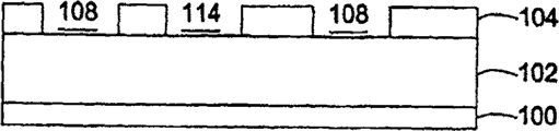
在衬底102上沉积无定型碳层104之后,无定型碳层104被图案化,以在其中包含特征108,如图2C所示。无定型碳层104可以通过在无定型碳层104上沉积和图案化光刻胶106来图案化,如图2B所示。在光刻胶106中图案化的特征107被转移到无定型碳层104中,以在无定型碳层104中创建特征108,并且光刻胶106被去除,如图2C所示。然后将光刻胶110沉积在无定型碳层上,并且将光刻胶110图案化以包括特征112,如图2D所示。在光刻胶110中图案化的特征112被转移到无定型碳层104,以在无定型碳层104中创建特征114,并且光刻胶110被去除,如图2E所示。无定型碳层104可以通过使用氧、氢和诸如NF3、SF6、CF4的含氟气体或其混合物的等离子体来刻蚀该层而被刻蚀。可选地,等离子体还可以包括HBr、N2、He、Ar或者其组合。然后使用无定型碳层作为掩模,将在无定型碳层中所图案化的特征108和114转移穿过衬底,以在衬底中形成特征116,如图2F所示。衬底可以通过将衬底暴露于适于衬底的组成的刻蚀剂来被图案化。在衬底被刻蚀之后,无定型碳层可以利用包含臭氧、氧、氨、氢或其组合的等离子体从衬底去除。After depositing the
在本文所描述的实施例中任何一个中,光刻胶可以使用常规技术来沉积、图案化和去除。例如,具有约2000埃到约6000埃之间的厚度的光刻胶层可以被沉积在衬底上。可以使用对于波长小于约450nm的UV辐射敏感的光刻胶或者对于波长为诸如248nm或193nm的辐射敏感的深紫外辐射抗蚀剂。光刻胶可以通过将光刻胶经过图案化的掩模暴露于适当波长的辐射来图案化。光刻胶可以通过等离子体灰化工艺去除。In any of the embodiments described herein, photoresist can be deposited, patterned, and removed using conventional techniques. For example, a photoresist layer having a thickness between about 2000 Angstroms and about 6000 Angstroms may be deposited on the substrate. A photoresist sensitive to UV radiation having a wavelength of less than about 450 nm or a deep ultraviolet radiation resist sensitive to radiation having a wavelength such as 248 nm or 193 nm may be used. The photoresist can be patterned by exposing the photoresist to radiation of the appropriate wavelength through a patterned mask. The photoresist can be removed by a plasma ashing process.
在另一个实施例中,诸如非碳基电介质层的非碳基层被沉积在上述的无定型碳层上,作为覆盖层。如在此所定义的,非碳基层包括小于约50at%的碳。可以使用的非碳基材料的示例包括无定型硅、氮化硅、氧氮化硅、氧化硅、掺杂氧化硅、氧碳化硅、碳化物、碳化硅、钛和氮化钛。非碳基层可以在诸如去除光刻胶的处理步骤中保护无定型碳层。非碳基层也可以充当抗反射涂层。选择非碳基层,使得在非碳基层和无定型碳层下方的衬底之间存在良好的刻蚀选择性。优选地,非碳基层具有约50埃到约500埃之间的厚度。优选地,非碳基层具有至少约200埃的厚度。In another embodiment, a non-carbon based layer, such as a non-carbon-based dielectric layer, is deposited on the aforementioned amorphous carbon layer as a capping layer. As defined herein, a non-carbon based layer includes less than about 50 at% carbon. Examples of non-carbon-based materials that may be used include amorphous silicon, silicon nitride, silicon oxynitride, silicon oxide, doped silicon oxide, silicon oxycarbide, carbide, silicon carbide, titanium, and titanium nitride. The non-carbon based layer can protect the amorphous carbon layer during processing steps such as photoresist removal. Non-carbon based layers can also act as anti-reflective coatings. The non-carbon based layer is selected such that there is good etch selectivity between the non-carbon based layer and the substrate below the amorphous carbon layer. Preferably, the non-carbon based layer has a thickness between about 50 Angstroms and about 500 Angstroms. Preferably, the non-carbon based layer has a thickness of at least about 200 Angstroms.
在无定型碳层上包括非碳基层作为覆盖层的实施例将参考图3A-3F来描述。上面参考图2A-2F所描述的方法可以被用于执行参考图3A-3F和图4A—4D所描述的实施例中的相应步骤。Embodiments including a non-carbon based layer as a capping layer on an amorphous carbon layer will be described with reference to FIGS. 3A-3F . The methods described above with reference to FIGS. 2A-2F may be used to perform corresponding steps in the embodiments described with reference to FIGS. 3A-3F and FIGS. 4A-4D .
无定型碳层204被沉积在衬底202上,如图3A所示。衬底202可以上覆于底层200。底层200可以是在衬底202的刻蚀过程中的用于衬底202的刻蚀停止层。非碳基层205沉积在无定型碳层204上。非碳基层205可以通过常规的方法来沉积,诸如化学气相沉积、物理气相沉积或者旋涂工艺。无定型碳层204和非碳基层205可以通过在非碳基层205上沉积和图案化光刻胶206来图案化,如图3B所示。在光刻胶206中图案化的特征207被转移到无定型碳层204和非碳基层205中,以在无定型碳层204和非碳基层205中创建特征208,并且光刻胶206被去除,如图3C所示。然后将光刻胶210沉积在无定型碳层上,并且将光刻胶210图案化以包括特征212,如图3D所示。在光刻胶210中图案化的特征212被转移到无定型碳层204和非碳基层205,以在无定型碳层204和非碳基层205中创建特征214,并且光刻胶210被去除,如图3E所示。然后使用无定型碳层作为掩模,将在无定型碳层中所图案化的特征208和214转移穿过衬底,以在衬底中形成特征216,如图3F所示。在特征被转移穿过衬底的同时或者在去除无定型碳层过程中,可以去除非碳基层。无定型碳层可以利用包含臭氧、氧、氨、氢或其组合的等离子体从衬底去除。
虽然在图3A-3F的实施例中的非碳基层205被图示和描述为在特征208形成在无定型碳层204中之后保留在衬底上,但是在其它实施例中,在特征208被形成在无定型碳层中之后(诸如在去除光刻胶206的过程中),可以去除非碳基层205的一部分或者全部。在一个实施例中,第二非碳基层被沉积在衬底上。第二非碳基层可以直接沉积在衬底上、沉积在第一非碳基层上、或者沉积在第一非碳基层的保留部分上。第二非碳基层可以包括无定型硅、氮化硅、氧化硅、掺杂氧化硅、氧碳化硅、碳化物、碳化硅、钛和氮化钛。第二非碳基层可以具有与第一非碳基层相同或者不同的组成。While the non-carbon-based
图4A-4D示出了其中在处理过程中第一非碳基层205的全部被去除的实施例。图4A对应于图3C,不同之处为第一非碳基层205已经被去除。然后,第二非碳基层220被沉积在无定型碳层204和暴露的衬底202上,并且光刻胶222被沉积在第二非碳基层220上,如图4B所示。光刻胶222被图案化以包括特征224,如图4C所示。在光刻胶206中图案化的特征224被转移到无定型碳层204和非碳基层220,以在无定型碳层204和非碳基层220中创建特征208,并且光刻胶222被去除,如图4所示。图4D基本上对应于图3E。然后刻蚀衬底202,如图3F所示。4A-4D illustrate an embodiment in which all of the first non-carbon based
在图2A-2F和3A-3F所示的实施例中,相同或基本相同的特征被形成在被图案化两次并且用作图案化衬底的硬掩模的无定型碳层中。优选地,第一掩模被用于在无定型碳层中形成第一图案,第二掩模被用于在无定型碳层中形成第二图案。In the embodiments shown in Figures 2A-2F and 3A-3F, the same or substantially the same features are formed in an amorphous carbon layer that is patterned twice and used as a hard mask for the patterned substrate. Preferably, a first mask is used to form a first pattern in the amorphous carbon layer and a second mask is used to form a second pattern in the amorphous carbon layer.
示例example
在

虽然上面所述的涉及本发明的实施例,但是可以设计本发明的其它和更多的实施例,而不偏离本发明的基本范围,本发明的基本范围有所附权利要求确定。While what has been described above relates to embodiments of the invention, other and further embodiments of the invention can be devised without departing from the essential scope of the invention, which is defined by the appended claims.
Claims (26)
Applications Claiming Priority (2)
| Application Number | Priority Date | Filing Date | Title |
|---|---|---|---|
| US10/768,724 | 2004-01-30 | ||
| US10/768,724 US7064078B2 (en) | 2004-01-30 | 2004-01-30 | Techniques for the use of amorphous carbon (APF) for various etch and litho integration scheme |
Publications (2)
| Publication Number | Publication Date |
|---|---|
| CN1914715A CN1914715A (en) | 2007-02-14 |
| CN100524640C true CN100524640C (en) | 2009-08-05 |
Family
ID=34807939
Family Applications (1)
| Application Number | Title | Priority Date | Filing Date |
|---|---|---|---|
| CNB2005800032995A Expired - Fee Related CN100524640C (en) | 2004-01-30 | 2005-01-07 | Techniques for the use of amorphous carbon(apf) for various etch and litho integration scheme |
Country Status (5)
| Country | Link |
|---|---|
| US (2) | US7064078B2 (en) |
| KR (1) | KR101155141B1 (en) |
| CN (1) | CN100524640C (en) |
| TW (1) | TWI428712B (en) |
| WO (1) | WO2005076337A1 (en) |
Families Citing this family (293)
| Publication number | Priority date | Publication date | Assignee | Title |
|---|---|---|---|---|
| US6541397B1 (en) * | 2002-03-29 | 2003-04-01 | Applied Materials, Inc. | Removable amorphous carbon CMP stop |
| KR100598038B1 (en) * | 2004-02-25 | 2006-07-07 | 삼성전자주식회사 | Solid-state image sensor containing a multilayer antireflection film, and its manufacturing method |
| US20050191584A1 (en) * | 2004-02-27 | 2005-09-01 | Kevin Shea | Surface treatment of a dry-developed hard mask and surface treatment compositions used therefor |
| US7355384B2 (en) * | 2004-04-08 | 2008-04-08 | International Business Machines Corporation | Apparatus, method, and computer program product for monitoring and controlling a microcomputer using a single existing pin |
| US7151040B2 (en) * | 2004-08-31 | 2006-12-19 | Micron Technology, Inc. | Methods for increasing photo alignment margins |
| US7910288B2 (en) | 2004-09-01 | 2011-03-22 | Micron Technology, Inc. | Mask material conversion |
| US7655387B2 (en) * | 2004-09-02 | 2010-02-02 | Micron Technology, Inc. | Method to align mask patterns |
| US7115525B2 (en) * | 2004-09-02 | 2006-10-03 | Micron Technology, Inc. | Method for integrated circuit fabrication using pitch multiplication |
| US7390746B2 (en) | 2005-03-15 | 2008-06-24 | Micron Technology, Inc. | Multiple deposition for integration of spacers in pitch multiplication process |
| US7253118B2 (en) | 2005-03-15 | 2007-08-07 | Micron Technology, Inc. | Pitch reduced patterns relative to photolithography features |
| US7611944B2 (en) | 2005-03-28 | 2009-11-03 | Micron Technology, Inc. | Integrated circuit fabrication |
| US7422775B2 (en) | 2005-05-17 | 2008-09-09 | Applied Materials, Inc. | Process for low temperature plasma deposition of an optical absorption layer and high speed optical annealing |
| US7312162B2 (en) | 2005-05-17 | 2007-12-25 | Applied Materials, Inc. | Low temperature plasma deposition process for carbon layer deposition |
| US7429536B2 (en) | 2005-05-23 | 2008-09-30 | Micron Technology, Inc. | Methods for forming arrays of small, closely spaced features |
| US7560390B2 (en) | 2005-06-02 | 2009-07-14 | Micron Technology, Inc. | Multiple spacer steps for pitch multiplication |
| US7396781B2 (en) * | 2005-06-09 | 2008-07-08 | Micron Technology, Inc. | Method and apparatus for adjusting feature size and position |
| KR100733421B1 (en) * | 2005-06-30 | 2007-06-29 | 주식회사 하이닉스반도체 | Manufacturing Method of Semiconductor Device |
| US7413981B2 (en) | 2005-07-29 | 2008-08-19 | Micron Technology, Inc. | Pitch doubled circuit layout |
| US7312148B2 (en) * | 2005-08-08 | 2007-12-25 | Applied Materials, Inc. | Copper barrier reflow process employing high speed optical annealing |
| US7335611B2 (en) | 2005-08-08 | 2008-02-26 | Applied Materials, Inc. | Copper conductor annealing process employing high speed optical annealing with a low temperature-deposited optical absorber layer |
| US7429532B2 (en) | 2005-08-08 | 2008-09-30 | Applied Materials, Inc. | Semiconductor substrate process using an optically writable carbon-containing mask |
| US7323401B2 (en) * | 2005-08-08 | 2008-01-29 | Applied Materials, Inc. | Semiconductor substrate process using a low temperature deposited carbon-containing hard mask |
| US8123968B2 (en) * | 2005-08-25 | 2012-02-28 | Round Rock Research, Llc | Multiple deposition for integration of spacers in pitch multiplication process |
| US7816262B2 (en) * | 2005-08-30 | 2010-10-19 | Micron Technology, Inc. | Method and algorithm for random half pitched interconnect layout with constant spacing |
| US7829262B2 (en) * | 2005-08-31 | 2010-11-09 | Micron Technology, Inc. | Method of forming pitch multipled contacts |
| US7572572B2 (en) | 2005-09-01 | 2009-08-11 | Micron Technology, Inc. | Methods for forming arrays of small, closely spaced features |
| US7759197B2 (en) | 2005-09-01 | 2010-07-20 | Micron Technology, Inc. | Method of forming isolated features using pitch multiplication |
| US7393789B2 (en) | 2005-09-01 | 2008-07-01 | Micron Technology, Inc. | Protective coating for planarization |
| US7776744B2 (en) | 2005-09-01 | 2010-08-17 | Micron Technology, Inc. | Pitch multiplication spacers and methods of forming the same |
| US7432210B2 (en) * | 2005-10-05 | 2008-10-07 | Applied Materials, Inc. | Process to open carbon based hardmask |
| US8664124B2 (en) | 2005-10-31 | 2014-03-04 | Novellus Systems, Inc. | Method for etching organic hardmasks |
| US7399712B1 (en) * | 2005-10-31 | 2008-07-15 | Novellus Systems, Inc. | Method for etching organic hardmasks |
| KR100663375B1 (en) * | 2006-01-18 | 2007-01-02 | 삼성전자주식회사 | Manufacturing Method of Semiconductor Device Adopting Metal Nitride Film as Gate Electrode |
| US7476933B2 (en) | 2006-03-02 | 2009-01-13 | Micron Technology, Inc. | Vertical gated access transistor |
| US7842558B2 (en) | 2006-03-02 | 2010-11-30 | Micron Technology, Inc. | Masking process for simultaneously patterning separate regions |
| US7662721B2 (en) * | 2006-03-15 | 2010-02-16 | Infineon Technologies Ag | Hard mask layer stack and a method of patterning |
| US20070231748A1 (en) * | 2006-03-29 | 2007-10-04 | Swaminathan Sivakumar | Patterning trenches in a photoresist layer with tight end-to-end separation |
| US7902074B2 (en) | 2006-04-07 | 2011-03-08 | Micron Technology, Inc. | Simplified pitch doubling process flow |
| US8003310B2 (en) | 2006-04-24 | 2011-08-23 | Micron Technology, Inc. | Masking techniques and templates for dense semiconductor fabrication |
| US7488685B2 (en) * | 2006-04-25 | 2009-02-10 | Micron Technology, Inc. | Process for improving critical dimension uniformity of integrated circuit arrays |
| EP1850369A1 (en) | 2006-04-28 | 2007-10-31 | STMicroelectronics S.r.l. | Manufacturing process of an organic mask for microelectronic industry |
| US7795149B2 (en) | 2006-06-01 | 2010-09-14 | Micron Technology, Inc. | Masking techniques and contact imprint reticles for dense semiconductor fabrication |
| US7723009B2 (en) | 2006-06-02 | 2010-05-25 | Micron Technology, Inc. | Topography based patterning |
| WO2008015212A1 (en) * | 2006-08-02 | 2008-02-07 | Koninklijke Philips Electronics N.V. | Novel hard mask structure for patterning features in semiconductor devices |
| US7611980B2 (en) | 2006-08-30 | 2009-11-03 | Micron Technology, Inc. | Single spacer process for multiplying pitch by a factor greater than two and related intermediate IC structures |
| US7959818B2 (en) | 2006-09-12 | 2011-06-14 | Hynix Semiconductor Inc. | Method for forming a fine pattern of a semiconductor device |
| US7666578B2 (en) | 2006-09-14 | 2010-02-23 | Micron Technology, Inc. | Efficient pitch multiplication process |
| US7811747B2 (en) * | 2006-09-22 | 2010-10-12 | Tokyo Electron Limited | Method of patterning an anti-reflective coating by partial developing |
| US7858293B2 (en) * | 2006-09-22 | 2010-12-28 | Tokyo Electron Limited | Method for double imaging a developable anti-reflective coating |
| KR100766239B1 (en) * | 2006-09-22 | 2007-10-10 | 주식회사 하이닉스반도체 | Metal interlayer insulating film formation method of semiconductor device |
| US7862985B2 (en) * | 2006-09-22 | 2011-01-04 | Tokyo Electron Limited | Method for double patterning a developable anti-reflective coating |
| US20080073321A1 (en) * | 2006-09-22 | 2008-03-27 | Tokyo Electron Limited | Method of patterning an anti-reflective coating by partial etching |
| US7883835B2 (en) * | 2006-09-22 | 2011-02-08 | Tokyo Electron Limited | Method for double patterning a thin film |
| US8168372B2 (en) * | 2006-09-25 | 2012-05-01 | Brewer Science Inc. | Method of creating photolithographic structures with developer-trimmed hard mask |
| KR100808056B1 (en) * | 2006-12-27 | 2008-02-28 | 주식회사 하이닉스반도체 | Pattern formation method using hard mask |
| JP5154140B2 (en) * | 2006-12-28 | 2013-02-27 | 東京エレクトロン株式会社 | Semiconductor device and manufacturing method thereof |
| US7767386B2 (en) * | 2007-01-15 | 2010-08-03 | Tokyo Electron Limited | Method of patterning an organic planarization layer |
| US7932017B2 (en) * | 2007-01-15 | 2011-04-26 | Tokyo Electron Limited | Method of double patterning a thin film using a developable anti-reflective coating and a developable organic planarization layer |
| JP5106020B2 (en) * | 2007-02-08 | 2012-12-26 | パナソニック株式会社 | Pattern formation method |
| JP2008227465A (en) * | 2007-02-14 | 2008-09-25 | Renesas Technology Corp | Method of manufacturing a semiconductor device |
| US7915166B1 (en) | 2007-02-22 | 2011-03-29 | Novellus Systems, Inc. | Diffusion barrier and etch stop films |
| KR100843239B1 (en) * | 2007-03-08 | 2008-07-03 | 삼성전자주식회사 | Micro pattern formation method of semiconductor device using double patterning process |
| US7943285B2 (en) * | 2007-03-13 | 2011-05-17 | Panasonic Corporation | Pattern formation method |
| KR100822592B1 (en) | 2007-03-23 | 2008-04-16 | 주식회사 하이닉스반도체 | Method of forming fine pattern of semiconductor device |
| US20080254233A1 (en) * | 2007-04-10 | 2008-10-16 | Kwangduk Douglas Lee | Plasma-induced charge damage control for plasma enhanced chemical vapor deposition processes |
| KR100866735B1 (en) * | 2007-05-01 | 2008-11-03 | 주식회사 하이닉스반도체 | Method of forming fine pattern of semiconductor device |
| TWI455203B (en) * | 2007-05-03 | 2014-10-01 | 蘭姆研究公司 | Hard mask of the opening and etching contour control by hard masking of the opening |
| CN101308330B (en) * | 2007-05-16 | 2010-12-15 | 上海华虹Nec电子有限公司 | Two time graph exposure method utilizing developing filler material |
| KR100777043B1 (en) * | 2007-05-22 | 2007-11-16 | 주식회사 테스 | Amorphous carbon film formation method and semiconductor device manufacturing method using same |
| US7807578B2 (en) * | 2007-06-01 | 2010-10-05 | Applied Materials, Inc. | Frequency doubling using spacer mask |
| US7901869B2 (en) * | 2007-06-01 | 2011-03-08 | Applied Materials, Inc. | Double patterning with a double layer cap on carbonaceous hardmask |
| US7846849B2 (en) * | 2007-06-01 | 2010-12-07 | Applied Materials, Inc. | Frequency tripling using spacer mask having interposed regions |
| US7923373B2 (en) * | 2007-06-04 | 2011-04-12 | Micron Technology, Inc. | Pitch multiplication using self-assembling materials |
| US20080303037A1 (en) * | 2007-06-04 | 2008-12-11 | Irving Lyn M | Methods of making thin film transistors comprising zinc-oxide-based semiconductor materials and transistors made thereby |
| US7553770B2 (en) * | 2007-06-06 | 2009-06-30 | Micron Technology, Inc. | Reverse masking profile improvements in high aspect ratio etch |
| KR20100039847A (en) * | 2007-06-15 | 2010-04-16 | 어플라이드 머티어리얼스, 인코포레이티드 | Oxygen sacvd to form sacrificial oxide liners in substrate gaps |
| US8337950B2 (en) * | 2007-06-19 | 2012-12-25 | Applied Materials, Inc. | Method for depositing boron-rich films for lithographic mask applications |
| US7718546B2 (en) | 2007-06-27 | 2010-05-18 | Sandisk 3D Llc | Method for fabricating a 3-D integrated circuit using a hard mask of silicon-oxynitride on amorphous carbon |
| US7858514B2 (en) | 2007-06-29 | 2010-12-28 | Qimonda Ag | Integrated circuit, intermediate structure and a method of fabricating a semiconductor structure |
| US20090023294A1 (en) * | 2007-07-16 | 2009-01-22 | Applied Materials, Inc. | Method for etching using advanced patterning film in capacitive coupling high frequency plasma dielectric etch chamber |
| JP4476313B2 (en) | 2007-07-25 | 2010-06-09 | 東京エレクトロン株式会社 | Film forming method, film forming apparatus, and storage medium |
| US7737049B2 (en) * | 2007-07-31 | 2010-06-15 | Qimonda Ag | Method for forming a structure on a substrate and device |
| US8563229B2 (en) | 2007-07-31 | 2013-10-22 | Micron Technology, Inc. | Process of semiconductor fabrication with mask overlay on pitch multiplied features and associated structures |
| US20090053620A1 (en) * | 2007-08-24 | 2009-02-26 | Hynix Semiconductor Inc. | Blank Mask and Method for Fabricating Photomask Using the Same |
| US8962101B2 (en) | 2007-08-31 | 2015-02-24 | Novellus Systems, Inc. | Methods and apparatus for plasma-based deposition |
| JP2009076661A (en) * | 2007-09-20 | 2009-04-09 | Elpida Memory Inc | Manufacturing method of semiconductor device |
| US20090087993A1 (en) * | 2007-09-28 | 2009-04-02 | Steven Maxwell | Methods and apparatus for cost-effectively increasing feature density using a mask shrinking process with double patterning |
| JP5671202B2 (en) * | 2007-10-26 | 2015-02-18 | アプライド マテリアルズ インコーポレイテッドApplied Materials,Incorporated | How to double the frequency using a photoresist template mask |
| US7737039B2 (en) | 2007-11-01 | 2010-06-15 | Micron Technology, Inc. | Spacer process for on pitch contacts and related structures |
| KR101344019B1 (en) * | 2007-11-01 | 2013-12-24 | 삼성전자주식회사 | Method of implatating ions |
| US7659208B2 (en) | 2007-12-06 | 2010-02-09 | Micron Technology, Inc | Method for forming high density patterns |
| US7790531B2 (en) | 2007-12-18 | 2010-09-07 | Micron Technology, Inc. | Methods for isolating portions of a loop of pitch-multiplied material and related structures |
| US8158334B2 (en) * | 2008-01-14 | 2012-04-17 | International Business Machines Corporation | Methods for forming a composite pattern including printed resolution assist features |
| JP5357186B2 (en) * | 2008-01-29 | 2013-12-04 | ブルーワー サイエンス アイ エヌ シー. | On-track process for hard mask pattern formation by multiple dark field exposure |
| JP5086283B2 (en) * | 2008-02-15 | 2012-11-28 | 東京エレクトロン株式会社 | Pattern forming method and semiconductor device manufacturing method |
| JP5254049B2 (en) * | 2008-02-15 | 2013-08-07 | 東京エレクトロン株式会社 | Pattern forming method and semiconductor device manufacturing method |
| JP2009194207A (en) * | 2008-02-15 | 2009-08-27 | Tokyo Electron Ltd | Pattern forming method, semiconductor device manufacturing method, and semiconductor device manufacturing apparatus |
| FR2927708A1 (en) * | 2008-02-19 | 2009-08-21 | Commissariat Energie Atomique | METHOD FOR ULTRAVIOLET IMMERSION PHOTOLITHOGRAPHY |
| US8030218B2 (en) * | 2008-03-21 | 2011-10-04 | Micron Technology, Inc. | Method for selectively modifying spacing between pitch multiplied structures |
| US8148269B2 (en) * | 2008-04-04 | 2012-04-03 | Applied Materials, Inc. | Boron nitride and boron-nitride derived materials deposition method |
| KR100919350B1 (en) * | 2008-04-24 | 2009-09-25 | 주식회사 하이닉스반도체 | Pattern formation method of semiconductor device |
| JP2009283674A (en) * | 2008-05-22 | 2009-12-03 | Elpida Memory Inc | Method of manufacturing semiconductor apparatus |
| US20090297731A1 (en) * | 2008-05-30 | 2009-12-03 | Asm Japan K.K. | Apparatus and method for improving production throughput in cvd chamber |
| US20090311634A1 (en) * | 2008-06-11 | 2009-12-17 | Tokyo Electron Limited | Method of double patterning using sacrificial structure |
| US8293460B2 (en) * | 2008-06-16 | 2012-10-23 | Applied Materials, Inc. | Double exposure patterning with carbonaceous hardmask |
| US8435608B1 (en) | 2008-06-27 | 2013-05-07 | Novellus Systems, Inc. | Methods of depositing smooth and conformal ashable hard mask films |
| US8076208B2 (en) | 2008-07-03 | 2011-12-13 | Micron Technology, Inc. | Method for forming transistor with high breakdown voltage using pitch multiplication technique |
| US8101497B2 (en) | 2008-09-11 | 2012-01-24 | Micron Technology, Inc. | Self-aligned trench formation |
| US8252653B2 (en) * | 2008-10-21 | 2012-08-28 | Applied Materials, Inc. | Method of forming a non-volatile memory having a silicon nitride charge trap layer |
| JP2010109148A (en) * | 2008-10-30 | 2010-05-13 | Toshiba Corp | Method of forming resist pattern |
| US8492282B2 (en) | 2008-11-24 | 2013-07-23 | Micron Technology, Inc. | Methods of forming a masking pattern for integrated circuits |
| US7972959B2 (en) * | 2008-12-01 | 2011-07-05 | Applied Materials, Inc. | Self aligned double patterning flow with non-sacrificial features |
| US9640396B2 (en) | 2009-01-07 | 2017-05-02 | Brewer Science Inc. | Spin-on spacer materials for double- and triple-patterning lithography |
| US8198671B2 (en) * | 2009-04-22 | 2012-06-12 | Applied Materials, Inc. | Modification of charge trap silicon nitride with oxygen plasma |
| TWI419201B (en) * | 2009-04-27 | 2013-12-11 | Macronix Int Co Ltd | Patterned method |
| US8519540B2 (en) | 2009-06-16 | 2013-08-27 | International Business Machines Corporation | Self-aligned dual damascene BEOL structures with patternable low- K material and methods of forming same |
| US8659115B2 (en) * | 2009-06-17 | 2014-02-25 | International Business Machines Corporation | Airgap-containing interconnect structure with improved patternable low-K material and method of fabricating |
| US8163658B2 (en) * | 2009-08-24 | 2012-04-24 | International Business Machines Corporation | Multiple patterning using improved patternable low-k dielectric materials |
| US8202783B2 (en) * | 2009-09-29 | 2012-06-19 | International Business Machines Corporation | Patternable low-k dielectric interconnect structure with a graded cap layer and method of fabrication |
| US8637395B2 (en) * | 2009-11-16 | 2014-01-28 | International Business Machines Corporation | Methods for photo-patternable low-k (PPLK) integration with curing after pattern transfer |
| US8367540B2 (en) * | 2009-11-19 | 2013-02-05 | International Business Machines Corporation | Interconnect structure including a modified photoresist as a permanent interconnect dielectric and method of fabricating same |
| TWI409852B (en) * | 2009-12-31 | 2013-09-21 | 華亞科技股份有限公司 | Method for fabricating semiconductor component fine structure by using self-aligned double pattern |
| US8642252B2 (en) | 2010-03-10 | 2014-02-04 | International Business Machines Corporation | Methods for fabrication of an air gap-containing interconnect structure |
| US8563414B1 (en) | 2010-04-23 | 2013-10-22 | Novellus Systems, Inc. | Methods for forming conductive carbon films by PECVD |
| US8896120B2 (en) | 2010-04-27 | 2014-11-25 | International Business Machines Corporation | Structures and methods for air gap integration |
| KR20130115085A (en) | 2010-04-30 | 2013-10-21 | 어플라이드 머티어리얼스, 인코포레이티드 | Amorphous carbon deposition method for improved stack defectivity |
| US8241992B2 (en) | 2010-05-10 | 2012-08-14 | International Business Machines Corporation | Method for air gap interconnect integration using photo-patternable low k material |
| US8373271B2 (en) | 2010-05-27 | 2013-02-12 | International Business Machines Corporation | Interconnect structure with an oxygen-doped SiC antireflective coating and method of fabrication |
| US9324576B2 (en) | 2010-05-27 | 2016-04-26 | Applied Materials, Inc. | Selective etch for silicon films |
| TW201216331A (en) | 2010-10-05 | 2012-04-16 | Applied Materials Inc | Ultra high selectivity doped amorphous carbon strippable hardmask development and integration |
| US10283321B2 (en) | 2011-01-18 | 2019-05-07 | Applied Materials, Inc. | Semiconductor processing system and methods using capacitively coupled plasma |
| US9064815B2 (en) | 2011-03-14 | 2015-06-23 | Applied Materials, Inc. | Methods for etch of metal and metal-oxide films |
| US8999856B2 (en) | 2011-03-14 | 2015-04-07 | Applied Materials, Inc. | Methods for etch of sin films |
| US8592321B2 (en) | 2011-06-08 | 2013-11-26 | United Microelectronics Corp. | Method for fabricating an aperture |
| US8641828B2 (en) | 2011-07-13 | 2014-02-04 | United Microelectronics Corp. | Cleaning method of semiconductor manufacturing process |
| US8808563B2 (en) | 2011-10-07 | 2014-08-19 | Applied Materials, Inc. | Selective etch of silicon by way of metastable hydrogen termination |
| US8557649B2 (en) | 2011-10-21 | 2013-10-15 | International Business Machines Corporation | Method for controlling structure height |
| US8962484B2 (en) * | 2011-12-16 | 2015-02-24 | Taiwan Semiconductor Manufacturing Company, Ltd. | Method of forming pattern for semiconductor device |
| SG193093A1 (en) * | 2012-02-13 | 2013-09-30 | Novellus Systems Inc | Method for etching organic hardmasks |
| SG195494A1 (en) | 2012-05-18 | 2013-12-30 | Novellus Systems Inc | Carbon deposition-etch-ash gap fill process |
| US9267739B2 (en) | 2012-07-18 | 2016-02-23 | Applied Materials, Inc. | Pedestal with multi-zone temperature control and multiple purge capabilities |
| US9373517B2 (en) | 2012-08-02 | 2016-06-21 | Applied Materials, Inc. | Semiconductor processing with DC assisted RF power for improved control |
| US10130767B2 (en) | 2012-08-30 | 2018-11-20 | Medtronic Minimed, Inc. | Sensor model supervisor for a closed-loop insulin infusion system |
| US9034770B2 (en) | 2012-09-17 | 2015-05-19 | Applied Materials, Inc. | Differential silicon oxide etch |
| US9023734B2 (en) | 2012-09-18 | 2015-05-05 | Applied Materials, Inc. | Radical-component oxide etch |
| US9390937B2 (en) | 2012-09-20 | 2016-07-12 | Applied Materials, Inc. | Silicon-carbon-nitride selective etch |
| US9132436B2 (en) | 2012-09-21 | 2015-09-15 | Applied Materials, Inc. | Chemical control features in wafer process equipment |
| US8969212B2 (en) | 2012-11-20 | 2015-03-03 | Applied Materials, Inc. | Dry-etch selectivity |
| US8980763B2 (en) | 2012-11-30 | 2015-03-17 | Applied Materials, Inc. | Dry-etch for selective tungsten removal |
| US9362133B2 (en) | 2012-12-14 | 2016-06-07 | Lam Research Corporation | Method for forming a mask by etching conformal film on patterned ashable hardmask |
| US9111877B2 (en) | 2012-12-18 | 2015-08-18 | Applied Materials, Inc. | Non-local plasma oxide etch |
| US8921234B2 (en) | 2012-12-21 | 2014-12-30 | Applied Materials, Inc. | Selective titanium nitride etching |
| US9299574B2 (en) | 2013-01-25 | 2016-03-29 | Applied Materials, Inc. | Silicon dioxide-polysilicon multi-layered stack etching with plasma etch chamber employing non-corrosive etchants |
| US9129911B2 (en) * | 2013-01-31 | 2015-09-08 | Applied Materials, Inc. | Boron-doped carbon-based hardmask etch processing |
| US10256079B2 (en) | 2013-02-08 | 2019-04-09 | Applied Materials, Inc. | Semiconductor processing systems having multiple plasma configurations |
| US9304396B2 (en) | 2013-02-25 | 2016-04-05 | Lam Research Corporation | PECVD films for EUV lithography |
| US9362130B2 (en) | 2013-03-01 | 2016-06-07 | Applied Materials, Inc. | Enhanced etching processes using remote plasma sources |
| US9040422B2 (en) | 2013-03-05 | 2015-05-26 | Applied Materials, Inc. | Selective titanium nitride removal |
| US20140271097A1 (en) | 2013-03-15 | 2014-09-18 | Applied Materials, Inc. | Processing systems and methods for halide scavenging |
| US9493879B2 (en) | 2013-07-12 | 2016-11-15 | Applied Materials, Inc. | Selective sputtering for pattern transfer |
| US9773648B2 (en) | 2013-08-30 | 2017-09-26 | Applied Materials, Inc. | Dual discharge modes operation for remote plasma |
| US9355820B2 (en) * | 2013-09-12 | 2016-05-31 | Applied Materials, Inc. | Methods for removing carbon containing films |
| US9589799B2 (en) | 2013-09-30 | 2017-03-07 | Lam Research Corporation | High selectivity and low stress carbon hardmask by pulsed low frequency RF power |
| US9320387B2 (en) | 2013-09-30 | 2016-04-26 | Lam Research Corporation | Sulfur doped carbon hard masks |
| US9576809B2 (en) | 2013-11-04 | 2017-02-21 | Applied Materials, Inc. | Etch suppression with germanium |
| US9396963B2 (en) * | 2013-11-06 | 2016-07-19 | Mattson Technology | Mask removal process strategy for vertical NAND device |
| US9520303B2 (en) | 2013-11-12 | 2016-12-13 | Applied Materials, Inc. | Aluminum selective etch |
| US9245762B2 (en) | 2013-12-02 | 2016-01-26 | Applied Materials, Inc. | Procedure for etch rate consistency |
| US9177797B2 (en) * | 2013-12-04 | 2015-11-03 | Taiwan Semiconductor Manufacturing Company, Ltd. | Lithography using high selectivity spacers for pitch reduction |
| JP2017507477A (en) * | 2014-01-08 | 2017-03-16 | アプライド マテリアルズ インコーポレイテッドApplied Materials,Incorporated | Development of high etching selectivity hard mask material by ion implantation into amorphous carbon film |
| US9396989B2 (en) | 2014-01-27 | 2016-07-19 | Applied Materials, Inc. | Air gaps between copper lines |
| US9385028B2 (en) | 2014-02-03 | 2016-07-05 | Applied Materials, Inc. | Air gap process |
| US9499898B2 (en) | 2014-03-03 | 2016-11-22 | Applied Materials, Inc. | Layered thin film heater and method of fabrication |
| US9299537B2 (en) | 2014-03-20 | 2016-03-29 | Applied Materials, Inc. | Radial waveguide systems and methods for post-match control of microwaves |
| US9299538B2 (en) | 2014-03-20 | 2016-03-29 | Applied Materials, Inc. | Radial waveguide systems and methods for post-match control of microwaves |
| US9903020B2 (en) | 2014-03-31 | 2018-02-27 | Applied Materials, Inc. | Generation of compact alumina passivation layers on aluminum plasma equipment components |
| US9309598B2 (en) | 2014-05-28 | 2016-04-12 | Applied Materials, Inc. | Oxide and metal removal |
| US9378969B2 (en) | 2014-06-19 | 2016-06-28 | Applied Materials, Inc. | Low temperature gas-phase carbon removal |
| US9406523B2 (en) | 2014-06-19 | 2016-08-02 | Applied Materials, Inc. | Highly selective doped oxide removal method |
| US20150371861A1 (en) * | 2014-06-23 | 2015-12-24 | Applied Materials, Inc. | Protective silicon oxide patterning |
| US9425058B2 (en) | 2014-07-24 | 2016-08-23 | Applied Materials, Inc. | Simplified litho-etch-litho-etch process |
| US9378978B2 (en) | 2014-07-31 | 2016-06-28 | Applied Materials, Inc. | Integrated oxide recess and floating gate fin trimming |
| US9496167B2 (en) | 2014-07-31 | 2016-11-15 | Applied Materials, Inc. | Integrated bit-line airgap formation and gate stack post clean |
| US9659753B2 (en) | 2014-08-07 | 2017-05-23 | Applied Materials, Inc. | Grooved insulator to reduce leakage current |
| US9553102B2 (en) | 2014-08-19 | 2017-01-24 | Applied Materials, Inc. | Tungsten separation |
| US9355856B2 (en) | 2014-09-12 | 2016-05-31 | Applied Materials, Inc. | V trench dry etch |
| US9368364B2 (en) | 2014-09-24 | 2016-06-14 | Applied Materials, Inc. | Silicon etch process with tunable selectivity to SiO2 and other materials |
| US9478434B2 (en) | 2014-09-24 | 2016-10-25 | Applied Materials, Inc. | Chlorine-based hardmask removal |
| US9613822B2 (en) | 2014-09-25 | 2017-04-04 | Applied Materials, Inc. | Oxide etch selectivity enhancement |
| US9966240B2 (en) | 2014-10-14 | 2018-05-08 | Applied Materials, Inc. | Systems and methods for internal surface conditioning assessment in plasma processing equipment |
| US9355922B2 (en) | 2014-10-14 | 2016-05-31 | Applied Materials, Inc. | Systems and methods for internal surface conditioning in plasma processing equipment |
| US11637002B2 (en) | 2014-11-26 | 2023-04-25 | Applied Materials, Inc. | Methods and systems to enhance process uniformity |
| US10573496B2 (en) | 2014-12-09 | 2020-02-25 | Applied Materials, Inc. | Direct outlet toroidal plasma source |
| US10224210B2 (en) | 2014-12-09 | 2019-03-05 | Applied Materials, Inc. | Plasma processing system with direct outlet toroidal plasma source |
| US9502258B2 (en) | 2014-12-23 | 2016-11-22 | Applied Materials, Inc. | Anisotropic gap etch |
| US9343272B1 (en) | 2015-01-08 | 2016-05-17 | Applied Materials, Inc. | Self-aligned process |
| US11257693B2 (en) | 2015-01-09 | 2022-02-22 | Applied Materials, Inc. | Methods and systems to improve pedestal temperature control |
| US9373522B1 (en) * | 2015-01-22 | 2016-06-21 | Applied Mateials, Inc. | Titanium nitride removal |
| US9449846B2 (en) | 2015-01-28 | 2016-09-20 | Applied Materials, Inc. | Vertical gate separation |
| US9928994B2 (en) | 2015-02-03 | 2018-03-27 | Lam Research Corporation | Methods for decreasing carbon-hydrogen content of amorphous carbon hardmask films |
| US9520295B2 (en) | 2015-02-03 | 2016-12-13 | Lam Research Corporation | Metal doping of amorphous carbon and silicon films used as hardmasks in substrate processing systems |
| US9728437B2 (en) | 2015-02-03 | 2017-08-08 | Applied Materials, Inc. | High temperature chuck for plasma processing systems |
| US20160225652A1 (en) | 2015-02-03 | 2016-08-04 | Applied Materials, Inc. | Low temperature chuck for plasma processing systems |
| US9881805B2 (en) | 2015-03-02 | 2018-01-30 | Applied Materials, Inc. | Silicon selective removal |
| KR102477091B1 (en) | 2015-07-24 | 2022-12-13 | 삼성전자주식회사 | Two-dimensional material hard mask, method of manufacturing the same and method of forming pattern of material layer using hard mask |
| KR20170016107A (en) | 2015-08-03 | 2017-02-13 | 삼성전자주식회사 | Method for fabricating semiconductor device |
| US9741593B2 (en) | 2015-08-06 | 2017-08-22 | Applied Materials, Inc. | Thermal management systems and methods for wafer processing systems |
| US9691645B2 (en) | 2015-08-06 | 2017-06-27 | Applied Materials, Inc. | Bolted wafer chuck thermal management systems and methods for wafer processing systems |
| US9349605B1 (en) | 2015-08-07 | 2016-05-24 | Applied Materials, Inc. | Oxide etch selectivity systems and methods |
| US10504700B2 (en) | 2015-08-27 | 2019-12-10 | Applied Materials, Inc. | Plasma etching systems and methods with secondary plasma injection |
| US10418243B2 (en) | 2015-10-09 | 2019-09-17 | Applied Materials, Inc. | Ultra-high modulus and etch selectivity boron-carbon hardmask films |
| CN106960816B (en) * | 2016-01-08 | 2019-09-27 | 中芯国际集成电路制造(上海)有限公司 | Double Graphical Method |
| US10504754B2 (en) | 2016-05-19 | 2019-12-10 | Applied Materials, Inc. | Systems and methods for improved semiconductor etching and component protection |
| US10522371B2 (en) | 2016-05-19 | 2019-12-31 | Applied Materials, Inc. | Systems and methods for improved semiconductor etching and component protection |
| US10128337B2 (en) * | 2016-06-03 | 2018-11-13 | Applied Materials, Inc. | Methods for forming fin structures with desired profile for 3D structure semiconductor applications |
| US9865484B1 (en) | 2016-06-29 | 2018-01-09 | Applied Materials, Inc. | Selective etch using material modification and RF pulsing |
| US10062575B2 (en) | 2016-09-09 | 2018-08-28 | Applied Materials, Inc. | Poly directional etch by oxidation |
| US10629473B2 (en) | 2016-09-09 | 2020-04-21 | Applied Materials, Inc. | Footing removal for nitride spacer |
| US10546729B2 (en) | 2016-10-04 | 2020-01-28 | Applied Materials, Inc. | Dual-channel showerhead with improved profile |
| US9721789B1 (en) | 2016-10-04 | 2017-08-01 | Applied Materials, Inc. | Saving ion-damaged spacers |
| US9934942B1 (en) | 2016-10-04 | 2018-04-03 | Applied Materials, Inc. | Chamber with flow-through source |
| US10062585B2 (en) | 2016-10-04 | 2018-08-28 | Applied Materials, Inc. | Oxygen compatible plasma source |
| US10062579B2 (en) | 2016-10-07 | 2018-08-28 | Applied Materials, Inc. | Selective SiN lateral recess |
| US9947549B1 (en) | 2016-10-10 | 2018-04-17 | Applied Materials, Inc. | Cobalt-containing material removal |
| US10163696B2 (en) | 2016-11-11 | 2018-12-25 | Applied Materials, Inc. | Selective cobalt removal for bottom up gapfill |
| US9768034B1 (en) | 2016-11-11 | 2017-09-19 | Applied Materials, Inc. | Removal methods for high aspect ratio structures |
| US10242908B2 (en) | 2016-11-14 | 2019-03-26 | Applied Materials, Inc. | Airgap formation with damage-free copper |
| US10026621B2 (en) | 2016-11-14 | 2018-07-17 | Applied Materials, Inc. | SiN spacer profile patterning |
| US10580661B2 (en) | 2016-12-14 | 2020-03-03 | Mattson Technology, Inc. | Atomic layer etch process using plasma in conjunction with a rapid thermal activation process |
| CN113658868B (en) | 2016-12-15 | 2023-08-08 | 联华电子股份有限公司 | Semiconductor element and manufacturing method thereof |
| EP4481811A3 (en) | 2016-12-23 | 2025-02-26 | Board Of Regents, The University Of Texas System | Heterogeneous integration of components onto compact devices using moiré based metrology and vacuum based pick-and-place |
| US10566206B2 (en) | 2016-12-27 | 2020-02-18 | Applied Materials, Inc. | Systems and methods for anisotropic material breakthrough |
| US10403507B2 (en) | 2017-02-03 | 2019-09-03 | Applied Materials, Inc. | Shaped etch profile with oxidation |
| US10431429B2 (en) | 2017-02-03 | 2019-10-01 | Applied Materials, Inc. | Systems and methods for radial and azimuthal control of plasma uniformity |
| US10043684B1 (en) | 2017-02-06 | 2018-08-07 | Applied Materials, Inc. | Self-limiting atomic thermal etching systems and methods |
| US10319739B2 (en) | 2017-02-08 | 2019-06-11 | Applied Materials, Inc. | Accommodating imperfectly aligned memory holes |
| US10943834B2 (en) | 2017-03-13 | 2021-03-09 | Applied Materials, Inc. | Replacement contact process |
| US10319649B2 (en) | 2017-04-11 | 2019-06-11 | Applied Materials, Inc. | Optical emission spectroscopy (OES) for remote plasma monitoring |
| JP7176860B6 (en) | 2017-05-17 | 2022-12-16 | アプライド マテリアルズ インコーポレイテッド | Semiconductor processing chamber to improve precursor flow |
| US11276559B2 (en) | 2017-05-17 | 2022-03-15 | Applied Materials, Inc. | Semiconductor processing chamber for multiple precursor flow |
| US11276590B2 (en) | 2017-05-17 | 2022-03-15 | Applied Materials, Inc. | Multi-zone semiconductor substrate supports |
| US10497579B2 (en) | 2017-05-31 | 2019-12-03 | Applied Materials, Inc. | Water-free etching methods |
| US10049891B1 (en) | 2017-05-31 | 2018-08-14 | Applied Materials, Inc. | Selective in situ cobalt residue removal |
| US10920320B2 (en) | 2017-06-16 | 2021-02-16 | Applied Materials, Inc. | Plasma health determination in semiconductor substrate processing reactors |
| US10541246B2 (en) | 2017-06-26 | 2020-01-21 | Applied Materials, Inc. | 3D flash memory cells which discourage cross-cell electrical tunneling |
| US10727080B2 (en) | 2017-07-07 | 2020-07-28 | Applied Materials, Inc. | Tantalum-containing material removal |
| US10541184B2 (en) | 2017-07-11 | 2020-01-21 | Applied Materials, Inc. | Optical emission spectroscopic techniques for monitoring etching |
| US10354889B2 (en) | 2017-07-17 | 2019-07-16 | Applied Materials, Inc. | Non-halogen etching of silicon-containing materials |
| US10170336B1 (en) | 2017-08-04 | 2019-01-01 | Applied Materials, Inc. | Methods for anisotropic control of selective silicon removal |
| US10043674B1 (en) | 2017-08-04 | 2018-08-07 | Applied Materials, Inc. | Germanium etching systems and methods |
| US10297458B2 (en) | 2017-08-07 | 2019-05-21 | Applied Materials, Inc. | Process window widening using coated parts in plasma etch processes |
| US10283324B1 (en) | 2017-10-24 | 2019-05-07 | Applied Materials, Inc. | Oxygen treatment for nitride etching |
| US10128086B1 (en) | 2017-10-24 | 2018-11-13 | Applied Materials, Inc. | Silicon pretreatment for nitride removal |
| KR102374206B1 (en) | 2017-12-05 | 2022-03-14 | 삼성전자주식회사 | Method of fabricating semiconductor device |
| US10256112B1 (en) | 2017-12-08 | 2019-04-09 | Applied Materials, Inc. | Selective tungsten removal |
| US10903054B2 (en) | 2017-12-19 | 2021-01-26 | Applied Materials, Inc. | Multi-zone gas distribution systems and methods |
| US11328909B2 (en) | 2017-12-22 | 2022-05-10 | Applied Materials, Inc. | Chamber conditioning and removal processes |
| US10854426B2 (en) | 2018-01-08 | 2020-12-01 | Applied Materials, Inc. | Metal recess for semiconductor structures |
| US10964512B2 (en) | 2018-02-15 | 2021-03-30 | Applied Materials, Inc. | Semiconductor processing chamber multistage mixing apparatus and methods |
| US10679870B2 (en) | 2018-02-15 | 2020-06-09 | Applied Materials, Inc. | Semiconductor processing chamber multistage mixing apparatus |
| TWI766433B (en) | 2018-02-28 | 2022-06-01 | 美商應用材料股份有限公司 | Systems and methods to form airgaps |
| US10593560B2 (en) | 2018-03-01 | 2020-03-17 | Applied Materials, Inc. | Magnetic induction plasma source for semiconductor processes and equipment |
| US10319600B1 (en) | 2018-03-12 | 2019-06-11 | Applied Materials, Inc. | Thermal silicon etch |
| US10497573B2 (en) | 2018-03-13 | 2019-12-03 | Applied Materials, Inc. | Selective atomic layer etching of semiconductor materials |
| US10573527B2 (en) | 2018-04-06 | 2020-02-25 | Applied Materials, Inc. | Gas-phase selective etching systems and methods |
| US10490406B2 (en) | 2018-04-10 | 2019-11-26 | Appled Materials, Inc. | Systems and methods for material breakthrough |
| US10699879B2 (en) | 2018-04-17 | 2020-06-30 | Applied Materials, Inc. | Two piece electrode assembly with gap for plasma control |
| KR102670420B1 (en) | 2018-04-24 | 2024-05-28 | 어플라이드 머티어리얼스, 인코포레이티드 | Plasma-enhanced chemical vapor deposition of carbon hard-masks |
| US10886137B2 (en) | 2018-04-30 | 2021-01-05 | Applied Materials, Inc. | Selective nitride removal |
| US10566194B2 (en) * | 2018-05-07 | 2020-02-18 | Lam Research Corporation | Selective deposition of etch-stop layer for enhanced patterning |
| US10755941B2 (en) | 2018-07-06 | 2020-08-25 | Applied Materials, Inc. | Self-limiting selective etching systems and methods |
| US10872778B2 (en) | 2018-07-06 | 2020-12-22 | Applied Materials, Inc. | Systems and methods utilizing solid-phase etchants |
| US10672642B2 (en) | 2018-07-24 | 2020-06-02 | Applied Materials, Inc. | Systems and methods for pedestal configuration |
| US10892198B2 (en) | 2018-09-14 | 2021-01-12 | Applied Materials, Inc. | Systems and methods for improved performance in semiconductor processing |
| US11049755B2 (en) | 2018-09-14 | 2021-06-29 | Applied Materials, Inc. | Semiconductor substrate supports with embedded RF shield |
| US11062887B2 (en) | 2018-09-17 | 2021-07-13 | Applied Materials, Inc. | High temperature RF heater pedestals |
| US11417534B2 (en) | 2018-09-21 | 2022-08-16 | Applied Materials, Inc. | Selective material removal |
| US11682560B2 (en) | 2018-10-11 | 2023-06-20 | Applied Materials, Inc. | Systems and methods for hafnium-containing film removal |
| US11121002B2 (en) | 2018-10-24 | 2021-09-14 | Applied Materials, Inc. | Systems and methods for etching metals and metal derivatives |
| US11437242B2 (en) | 2018-11-27 | 2022-09-06 | Applied Materials, Inc. | Selective removal of silicon-containing materials |
| US11195923B2 (en) | 2018-12-21 | 2021-12-07 | Applied Materials, Inc. | Method of fabricating a semiconductor device having reduced contact resistance |
| US11721527B2 (en) | 2019-01-07 | 2023-08-08 | Applied Materials, Inc. | Processing chamber mixing systems |
| US10920319B2 (en) | 2019-01-11 | 2021-02-16 | Applied Materials, Inc. | Ceramic showerheads with conductive electrodes |
| US11837441B2 (en) | 2019-05-29 | 2023-12-05 | Lam Research Corporation | Depositing a carbon hardmask by high power pulsed low frequency RF |
| KR102888630B1 (en) | 2019-08-30 | 2025-11-19 | 램 리써치 코포레이션 | High-density, high-modulus, and high-hardness amorphous carbon films at low pressure |
| US11562909B2 (en) | 2020-05-22 | 2023-01-24 | Applied Materials, Inc. | Directional selective junction clean with field polymer protections |
| US11715640B2 (en) | 2020-09-30 | 2023-08-01 | Taiwan Semiconductor Manufacturing Company, Ltd. | Patterning material including silicon-containing layer and method for semiconductor device fabrication |
| US20220102200A1 (en) * | 2020-09-30 | 2022-03-31 | Taiwan Semiconductor Manufacturing Company, Ltd. | Patterning material including carbon-containing layer and method for semiconductor device fabrication |
| CN113078105B (en) * | 2021-03-29 | 2022-07-05 | 长鑫存储技术有限公司 | Preparation method of mask structure, semiconductor structure and preparation method thereof |
| US11776810B2 (en) | 2021-08-31 | 2023-10-03 | Taiwan Semiconductor Manufacturing Co., Ltd. | Method of forming a semiconductor device |
| US12431362B2 (en) | 2022-05-06 | 2025-09-30 | Tokyo Electron Limited | Method for etching high aspect ratio features within a dielectric using a hard mask stack having multiple hard mask layers |
| CN117954310A (en) * | 2024-01-30 | 2024-04-30 | 浙江创芯集成电路有限公司 | Mask layer structure and forming method thereof and forming method of semiconductor structure |
| US20250253158A1 (en) * | 2024-02-05 | 2025-08-07 | Applied Materials, Inc. | Dry deposition of extreme ultraviolet (euv) underlayer for lithography and patterning |
Citations (7)
| Publication number | Priority date | Publication date | Assignee | Title |
|---|---|---|---|---|
| CN1211067A (en) * | 1997-09-08 | 1999-03-17 | 西门子公司 | Method for fabricating structures with large aspect ratios |
| US6140226A (en) * | 1998-01-16 | 2000-10-31 | International Business Machines Corporation | Dual damascene processing for semiconductor chip interconnects |
| US20020001778A1 (en) * | 2000-06-08 | 2002-01-03 | Applied Materials, Inc. | Photolithography scheme using a silicon containing resist |
| CN1349245A (en) * | 2000-10-17 | 2002-05-15 | 联华电子股份有限公司 | Method for improving side profile of photoresist pattern |
| US6498105B1 (en) * | 1999-06-01 | 2002-12-24 | Samsung Electronics Co., Ltd. | Method of forming fine patterns of a semiconductor device |
| US20030207207A1 (en) * | 2002-05-03 | 2003-11-06 | Weimin Li | Method of fabricating a semiconductor multilevel interconnect structure |
| US6653735B1 (en) * | 2002-07-30 | 2003-11-25 | Advanced Micro Devices, Inc. | CVD silicon carbide layer as a BARC and hard mask for gate patterning |
Family Cites Families (49)
| Publication number | Priority date | Publication date | Assignee | Title |
|---|---|---|---|---|
| JPH0258221A (en) | 1988-08-23 | 1990-02-27 | Semiconductor Energy Lab Co Ltd | Etching method using carbon or mask mainly comprising carbon |
| EP0381109A3 (en) | 1989-02-01 | 1990-12-12 | Siemens Aktiengesellschaft | Moisture barrier for organic dielectrics |
| DE69033996T2 (en) | 1989-04-28 | 2002-12-05 | Fujitsu Ltd., Kawasaki | Mask, method of making the mask and method of making a pattern with a mask |
| DE69005938T2 (en) | 1989-07-31 | 1994-05-19 | Matsushita Electric Ind Co Ltd | Device for producing a thin diamond-like carbon layer. |
| US5308741A (en) | 1992-07-31 | 1994-05-03 | Motorola, Inc. | Lithographic method using double exposure techniques, mask position shifting and light phase shifting |
| TW366367B (en) | 1995-01-26 | 1999-08-11 | Ibm | Sputter deposition of hydrogenated amorphous carbon film |
| TW302507B (en) | 1995-02-10 | 1997-04-11 | Siemens Ag | |
| JP3361918B2 (en) | 1995-07-26 | 2003-01-07 | 沖電気工業株式会社 | Method for forming fine holes in semiconductor integrated circuit device |
| US5759746A (en) | 1996-05-24 | 1998-06-02 | Kabushiki Kaisha Toshiba | Fabrication process using a thin resist |
| JPH1126578A (en) | 1997-07-02 | 1999-01-29 | Sony Corp | Method of forming fine connection holes |
| US6133618A (en) | 1997-08-14 | 2000-10-17 | Lucent Technologies Inc. | Semiconductor device having an anti-reflective layer and a method of manufacture thereof |
| US6143476A (en) | 1997-12-12 | 2000-11-07 | Applied Materials Inc | Method for high temperature etching of patterned layers using an organic mask stack |
| TWI246633B (en) | 1997-12-12 | 2006-01-01 | Applied Materials Inc | Method of pattern etching a low k dielectric layen |
| WO1999054922A1 (en) | 1998-04-22 | 1999-10-28 | Nikon Corporation | Exposure method and exposure system |
| US6184572B1 (en) | 1998-04-29 | 2001-02-06 | Novellus Systems, Inc. | Interlevel dielectric stack containing plasma deposited fluorinated amorphous carbon films for semiconductor devices |
| US6316167B1 (en) | 2000-01-10 | 2001-11-13 | International Business Machines Corporation | Tunabale vapor deposited materials as antireflective coatings, hardmasks and as combined antireflective coating/hardmasks and methods of fabrication thereof and application thereof |
| JP3123548B2 (en) * | 1998-06-30 | 2001-01-15 | キヤノン株式会社 | Exposure method and exposure apparatus |
| US6245662B1 (en) | 1998-07-23 | 2001-06-12 | Applied Materials, Inc. | Method of producing an interconnect structure for an integrated circuit |
| JP3531666B2 (en) | 1999-03-19 | 2004-05-31 | シャープ株式会社 | Phase shift mask and method of manufacturing the same |
| KR100307629B1 (en) | 1999-04-30 | 2001-09-26 | 윤종용 | Method for forming and applicating a anti reflective film using hydrocarbon based gas |
| US6821571B2 (en) * | 1999-06-18 | 2004-11-23 | Applied Materials Inc. | Plasma treatment to enhance adhesion and to minimize oxidation of carbon-containing layers |
| US6423384B1 (en) | 1999-06-25 | 2002-07-23 | Applied Materials, Inc. | HDP-CVD deposition of low dielectric constant amorphous carbon film |
| KR100304708B1 (en) | 1999-07-14 | 2001-11-01 | 윤종용 | Semiconductor device having a double layer type anti-reflective coating &fabricating method thereof |
| US6238850B1 (en) | 1999-08-23 | 2001-05-29 | International Business Machines Corp. | Method of forming sharp corners in a photoresist layer |
| US6265319B1 (en) * | 1999-09-01 | 2001-07-24 | Taiwan Semiconductor Manufacturing Company | Dual damascene method employing spin-on polymer (SOP) etch stop layer |
| US6573030B1 (en) | 2000-02-17 | 2003-06-03 | Applied Materials, Inc. | Method for depositing an amorphous carbon layer |
| US20020086547A1 (en) | 2000-02-17 | 2002-07-04 | Applied Materials, Inc. | Etch pattern definition using a CVD organic layer as an anti-reflection coating and hardmask |
| US6511791B1 (en) | 2000-04-28 | 2003-01-28 | International Business Machines Corporation | Multiple exposure process for formation of dense rectangular arrays |
| KR100669862B1 (en) | 2000-11-13 | 2007-01-17 | 삼성전자주식회사 | Method of forming fine pattern of semiconductor device |
| DE10100822C2 (en) | 2001-01-10 | 2003-04-10 | Infineon Technologies Ag | Plasma etching process for MoSi (ON) layers |
| KR100815222B1 (en) | 2001-02-27 | 2008-03-19 | 에이에스엠엘 유에스, 인크. | A method of exposing a field on a substrate stage with an image from a lithographic apparatus and at least two patterns formed on at least one reticle |
| US6548347B2 (en) | 2001-04-12 | 2003-04-15 | Micron Technology, Inc. | Method of forming minimally spaced word lines |
| JP2002351046A (en) | 2001-05-24 | 2002-12-04 | Nec Corp | Phase shift mask and design method thereof |
| US7226853B2 (en) * | 2001-12-26 | 2007-06-05 | Applied Materials, Inc. | Method of forming a dual damascene structure utilizing a three layer hard mask structure |
| DE10307518B4 (en) | 2002-02-22 | 2011-04-14 | Hoya Corp. | Halftone phase shift mask blank, halftone phase shift mask and method of making the same |
| US6541397B1 (en) * | 2002-03-29 | 2003-04-01 | Applied Materials, Inc. | Removable amorphous carbon CMP stop |
| US20040072081A1 (en) | 2002-05-14 | 2004-04-15 | Coleman Thomas P. | Methods for etching photolithographic reticles |
| US6818141B1 (en) * | 2002-06-10 | 2004-11-16 | Advanced Micro Devices, Inc. | Application of the CVD bilayer ARC as a hard mask for definition of the subresolution trench features between polysilicon wordlines |
| US6835663B2 (en) | 2002-06-28 | 2004-12-28 | Infineon Technologies Ag | Hardmask of amorphous carbon-hydrogen (a-C:H) layers with tunable etch resistivity |
| US6673684B1 (en) * | 2002-07-31 | 2004-01-06 | Advanced Micro Devices, Inc. | Use of diamond as a hard mask material |
| US6764949B2 (en) | 2002-07-31 | 2004-07-20 | Advanced Micro Devices, Inc. | Method for reducing pattern deformation and photoresist poisoning in semiconductor device fabrication |
| US6939808B2 (en) | 2002-08-02 | 2005-09-06 | Applied Materials, Inc. | Undoped and fluorinated amorphous carbon film as pattern mask for metal etch |
| US20040038537A1 (en) | 2002-08-20 | 2004-02-26 | Wei Liu | Method of preventing or suppressing sidewall buckling of mask structures used to etch feature sizes smaller than 50nm |
| US6853043B2 (en) * | 2002-11-04 | 2005-02-08 | Applied Materials, Inc. | Nitrogen-free antireflective coating for use with photolithographic patterning |
| US6787452B2 (en) * | 2002-11-08 | 2004-09-07 | Chartered Semiconductor Manufacturing Ltd. | Use of amorphous carbon as a removable ARC material for dual damascene fabrication |
| US20040166691A1 (en) | 2003-02-26 | 2004-08-26 | Chun-Feng Nieh | Method of etching a metal line |
| US20040180551A1 (en) | 2003-03-13 | 2004-09-16 | Biles Peter John | Carbon hard mask for aluminum interconnect fabrication |
| KR100641952B1 (en) | 2004-02-06 | 2006-11-02 | 주식회사 하이닉스반도체 | Method of forming fine pattern of semiconductor device |
| US8293430B2 (en) | 2005-01-27 | 2012-10-23 | Applied Materials, Inc. | Method for etching a molybdenum layer suitable for photomask fabrication |
-
2004
- 2004-01-30 US US10/768,724 patent/US7064078B2/en not_active Expired - Lifetime
-
2005
- 2005-01-07 CN CNB2005800032995A patent/CN100524640C/en not_active Expired - Fee Related
- 2005-01-07 WO PCT/US2005/000395 patent/WO2005076337A1/en not_active Ceased
- 2005-01-07 KR KR1020067017385A patent/KR101155141B1/en not_active Expired - Lifetime
- 2005-01-17 TW TW094101346A patent/TWI428712B/en not_active IP Right Cessation
-
2006
- 2006-06-02 US US11/422,031 patent/US7718081B2/en not_active Expired - Fee Related
Patent Citations (7)
| Publication number | Priority date | Publication date | Assignee | Title |
|---|---|---|---|---|
| CN1211067A (en) * | 1997-09-08 | 1999-03-17 | 西门子公司 | Method for fabricating structures with large aspect ratios |
| US6140226A (en) * | 1998-01-16 | 2000-10-31 | International Business Machines Corporation | Dual damascene processing for semiconductor chip interconnects |
| US6498105B1 (en) * | 1999-06-01 | 2002-12-24 | Samsung Electronics Co., Ltd. | Method of forming fine patterns of a semiconductor device |
| US20020001778A1 (en) * | 2000-06-08 | 2002-01-03 | Applied Materials, Inc. | Photolithography scheme using a silicon containing resist |
| CN1349245A (en) * | 2000-10-17 | 2002-05-15 | 联华电子股份有限公司 | Method for improving side profile of photoresist pattern |
| US20030207207A1 (en) * | 2002-05-03 | 2003-11-06 | Weimin Li | Method of fabricating a semiconductor multilevel interconnect structure |
| US6653735B1 (en) * | 2002-07-30 | 2003-11-25 | Advanced Micro Devices, Inc. | CVD silicon carbide layer as a BARC and hard mask for gate patterning |
Also Published As
| Publication number | Publication date |
|---|---|
| CN1914715A (en) | 2007-02-14 |
| WO2005076337A1 (en) | 2005-08-18 |
| US20050167394A1 (en) | 2005-08-04 |
| TWI428712B (en) | 2014-03-01 |
| US7064078B2 (en) | 2006-06-20 |
| TW200527165A (en) | 2005-08-16 |
| KR20060129412A (en) | 2006-12-15 |
| KR101155141B1 (en) | 2012-07-06 |
| US20060231524A1 (en) | 2006-10-19 |
| US7718081B2 (en) | 2010-05-18 |
Similar Documents
| Publication | Publication Date | Title |
|---|---|---|
| CN100524640C (en) | Techniques for the use of amorphous carbon(apf) for various etch and litho integration scheme | |
| US10014174B2 (en) | Conformal strippable carbon film for line-edge-roughness reduction for advanced patterning | |
| US20220367186A1 (en) | Patterning scheme to improve euv resist and hard mask selectivity | |
| CN108475640B (en) | Mixed carbon hard die for lateral hard die groove reduction | |
| US10410878B2 (en) | Hydrofluorocarbons containing —NH2 functional group for 3D NAND and DRAM applications | |
| CN1814857B (en) | Method for sputtering a protective coating on a semiconductor substrate | |
| CN1953146B (en) | Process to open carbon based hardmask | |
| KR101476435B1 (en) | Multi-layer resist plasma etch method | |
| US20040157444A1 (en) | Photoresist intensive patterning and processing | |
| US11605539B2 (en) | Defect correction on metal resists | |
| WO2012048108A2 (en) | Radiation patternable cvd film | |
| US20040072081A1 (en) | Methods for etching photolithographic reticles | |
| JP7778835B2 (en) | High density carbon films for patterning applications | |
| KR20060127250A (en) | Amorphous Carbon Film Deposition Method for Metal Etch Hardmask Applications | |
| KR20090119266A (en) | Thin film pattern formation method | |
| JP2005045053A (en) | Method for manufacturing semiconductor device | |
| CN110444475A (en) | Critical Dimension Trimming Method for Minimizing Line Width Roughness and Line Edge Roughness | |
| TWI332230B (en) | A method for selectively etching organosilicate glass with respect to a doped silicon carbide |
Legal Events
| Date | Code | Title | Description |
|---|---|---|---|
| C06 | Publication | ||
| PB01 | Publication | ||
| C10 | Entry into substantive examination | ||
| SE01 | Entry into force of request for substantive examination | ||
| C14 | Grant of patent or utility model | ||
| GR01 | Patent grant | ||
| CF01 | Termination of patent right due to non-payment of annual fee |
Granted publication date: 20090805 Termination date: 20150107 |
|
| EXPY | Termination of patent right or utility model |