KR100815222B1 - A method of exposing a field on a substrate stage with an image from a lithographic apparatus and at least two patterns formed on at least one reticle - Google Patents
A method of exposing a field on a substrate stage with an image from a lithographic apparatus and at least two patterns formed on at least one reticle Download PDFInfo
- Publication number
- KR100815222B1 KR100815222B1 KR1020027014433A KR20027014433A KR100815222B1 KR 100815222 B1 KR100815222 B1 KR 100815222B1 KR 1020027014433 A KR1020027014433 A KR 1020027014433A KR 20027014433 A KR20027014433 A KR 20027014433A KR 100815222 B1 KR100815222 B1 KR 100815222B1
- Authority
- KR
- South Korea
- Prior art keywords
- image
- reticle
- patterns
- substrate stage
- scanning
- Prior art date
- Legal status (The legal status is an assumption and is not a legal conclusion. Google has not performed a legal analysis and makes no representation as to the accuracy of the status listed.)
- Expired - Fee Related
Links
Images


Classifications
-
- G—PHYSICS
- G03—PHOTOGRAPHY; CINEMATOGRAPHY; ANALOGOUS TECHNIQUES USING WAVES OTHER THAN OPTICAL WAVES; ELECTROGRAPHY; HOLOGRAPHY
- G03F—PHOTOMECHANICAL PRODUCTION OF TEXTURED OR PATTERNED SURFACES, e.g. FOR PRINTING, FOR PROCESSING OF SEMICONDUCTOR DEVICES; MATERIALS THEREFOR; ORIGINALS THEREFOR; APPARATUS SPECIALLY ADAPTED THEREFOR
- G03F7/00—Photomechanical, e.g. photolithographic, production of textured or patterned surfaces, e.g. printing surfaces; Materials therefor, e.g. comprising photoresists; Apparatus specially adapted therefor
- G03F7/20—Exposure; Apparatus therefor
-
- G—PHYSICS
- G03—PHOTOGRAPHY; CINEMATOGRAPHY; ANALOGOUS TECHNIQUES USING WAVES OTHER THAN OPTICAL WAVES; ELECTROGRAPHY; HOLOGRAPHY
- G03F—PHOTOMECHANICAL PRODUCTION OF TEXTURED OR PATTERNED SURFACES, e.g. FOR PRINTING, FOR PROCESSING OF SEMICONDUCTOR DEVICES; MATERIALS THEREFOR; ORIGINALS THEREFOR; APPARATUS SPECIALLY ADAPTED THEREFOR
- G03F7/00—Photomechanical, e.g. photolithographic, production of textured or patterned surfaces, e.g. printing surfaces; Materials therefor, e.g. comprising photoresists; Apparatus specially adapted therefor
- G03F7/70—Microphotolithographic exposure; Apparatus therefor
- G03F7/70216—Mask projection systems
- G03F7/70283—Mask effects on the imaging process
-
- G—PHYSICS
- G03—PHOTOGRAPHY; CINEMATOGRAPHY; ANALOGOUS TECHNIQUES USING WAVES OTHER THAN OPTICAL WAVES; ELECTROGRAPHY; HOLOGRAPHY
- G03F—PHOTOMECHANICAL PRODUCTION OF TEXTURED OR PATTERNED SURFACES, e.g. FOR PRINTING, FOR PROCESSING OF SEMICONDUCTOR DEVICES; MATERIALS THEREFOR; ORIGINALS THEREFOR; APPARATUS SPECIALLY ADAPTED THEREFOR
- G03F7/00—Photomechanical, e.g. photolithographic, production of textured or patterned surfaces, e.g. printing surfaces; Materials therefor, e.g. comprising photoresists; Apparatus specially adapted therefor
- G03F7/70—Microphotolithographic exposure; Apparatus therefor
- G03F7/70216—Mask projection systems
- G03F7/70358—Scanning exposure, i.e. relative movement of patterned beam and workpiece during imaging
Landscapes
- Physics & Mathematics (AREA)
- General Physics & Mathematics (AREA)
- Exposure Of Semiconductors, Excluding Electron Or Ion Beam Exposure (AREA)
- Exposure And Positioning Against Photoresist Photosensitive Materials (AREA)
Abstract
본 발명은 기판 상으로 적어도 두개의 레티클을 동시에 이미지화하기 위한 방법 및 장치를 제공한다. 본 발명에 따르면, 웨이퍼는 일단 레티클로부터 이미지가 웨이퍼 상으로 동시에 노출된 채 노출 순서를 통과한다. 장치의 처리율은 표준 단일 패스 처리율 수준 또는 종래 장치 처리율의 2배에서 효과적으로 유지된다. 일 실시예에서, 본 발명은 스텝 및 스캔 웨이퍼 노출 장치의 광학계들의 출구 퓨필에 나란히 있는 2개의 레티클 이미지를 형성한다. 노출 툴의 스캐닝 작용은 그후에 웨이퍼의 노출 중 두개의 이미지를 효과적으로 중첩한다. 웨이퍼가 레티클의 스캐닝과 동시에 이미지 필드를 통하여 스캔됨에 따라 각 이미지는 포토레지스트를 노출시킨다. 일 실시예에 따르면, 이미지 스캐닝은 2개의 요구되는 이미지가 중첩되도록 동기된다. 또 다른 실시예에 따르면, 2개의 이미지는 독립적으로 집속될 수 있고 정렬될 수 있다.

레티클, 이미지, 노출, 이중, 리소그래피, 스캐닝
The present invention provides a method and apparatus for simultaneously imaging at least two reticles onto a substrate. According to the present invention, the wafer once passes through the exposure sequence with the image being simultaneously exposed onto the wafer from the reticle. The throughput of the device is effectively maintained at a standard single pass throughput level or twice the conventional device throughput. In one embodiment, the invention forms two reticle images parallel to the exit pupil of the optics of the step and scan wafer exposure apparatus. The scanning action of the exposure tool then effectively overlaps two images during the exposure of the wafer. Each image exposes the photoresist as the wafer is scanned through the image field simultaneously with scanning of the reticle. According to one embodiment, image scanning is synchronized such that the two required images overlap. According to yet another embodiment, the two images can be focused and aligned independently.
Reticle, image, exposure, double, lithography, scanning
Description
본 발명은 포토리소그래피에 관한 것이다.The present invention relates to photolithography.
금속, 부도체 및 반도체(즉, 디바이스)에 매우 미세한 패턴을 만드는데 사용하는 여러가지 포토리소그래피 또는 마이크로리소그래피 기술들이 있다. 포토리소그래피 혹은 마이크로리소그래피 공정에서 레티클 상에 포함되는 패턴(예를 들면, 회로 패턴)은 웨이퍼 상으로 투사된다.(즉, 이미지가 된다) 웨이퍼는 디바이스 또는 디바이스들을 형성하기 위하여 더 처리되는 전형적으로는 포토레지스트 기판이다.There are several photolithography or microlithography techniques used to make very fine patterns in metals, insulators and semiconductors (ie devices). In photolithography or microlithography processes, patterns (e.g., circuit patterns) included on the reticle are projected onto the wafer (i.e., become images). The wafer is typically further processed to form a device or devices. Photoresist substrate.
최소 배선폭 요구조건이 축소되는 것을 계속함에 따라 위상 이동 레티클의 사용은 증가해 왔다. 위상 이동 레티클은 리소그래피 장치의 유효 해상도를 증가시킨다. 위상 이동 기술들의 사용은 먼저 위상 이동 레티클로 그 다음에 트림 레티클로 웨이퍼 상의 동일한 필드 또는 영역의 노출을 전형적으로 요구한다. 트림 레티클은 이행에 따라 위상 이동 레티클과 다를 수 있다.As the minimum wire width requirement continues to shrink, the use of phase shift reticles has increased. The phase shift reticle increases the effective resolution of the lithographic apparatus. The use of phase shift techniques typically requires exposure of the same field or area on the wafer first with a phase shift reticle and then with a trim reticle. The trim reticle may differ from the phase shift reticle depending on the transition.
이러한 2단계 이미지화와 같은 기술들은 정렬 문제들을 유발할 수 있다. 그들은 또한 장치의 전체적인 웨이퍼 처리율을 감소시킬 수 있다.(즉, 그 장치는 각 웨이퍼가 두 번 노출되는 것이 필요하기 때문에 느려진다) 각 레티클은 주어진 웨이퍼 상의 노출용으로 설정됨에 따라 정밀 정렬 처리는 추가적인 시간을 소비하고, 종종 장치의 효율과 양품률을 감소시킨다.Techniques such as two-stage imaging can cause alignment problems. They can also reduce the overall wafer throughput of the device (i.e., the device slows down because each wafer needs to be exposed twice). As each reticle is set up for exposure on a given wafer, the precision alignment process takes additional time. Consume, and often reduce the efficiency and yield of the device.
필요한 것은 적어도 2개의 상이한 레티클로 동일한 필드를 동시에 노출시키는 방법과 장치이다. 더군다나, 필요한 것은 정렬 및 교정 문제들이 방지될 수 있도록 동시에 적어도 2개의 상이한 레티클로 동일한 필드를 노출시키는 방법과 장치이다.What is needed is a method and apparatus for simultaneously exposing the same field with at least two different reticles. Furthermore, what is needed is a method and apparatus that simultaneously expose the same field with at least two different reticles so that alignment and calibration problems can be avoided.
본 발명은 전술한 요구조건에 부합하는 방법과 장치를 제공한다. 본 발명의 방법과 장치는 노출 및/또는 축소 장치의 투사 광학계의 출구 퓨필(exit pupil)에 나란히 있는 2개의 레티클 이미지를 만든다. The present invention provides a method and apparatus that meet the above requirements. The method and apparatus of the present invention produce two reticle images that are parallel to the exit pupil of the projection optics of the exposure and / or reduction device.
일 실시예에서, 노출 장치는 스텝 및 스캔 웨이퍼 노출 장치이다. 이러한 실시예에서, 노출 툴의 스캐닝 동작은 웨이퍼의 노출 동안에 2개의 이미지를 효과적으로 중첩한다. 이에 따라, 레티클의 스캐닝과 동기 방법으로 이미지 필드를 통하여 웨이퍼가 스캔됨에 따라 각 이미지는 포토레지스트를 노출시킨다. 바꾸어 말하면, 스캔하는 이미지는 2개의 요구되는 레티클 이미지가 중첩되도록 동기된다. 본 발명의 추가적인 실시예에서, 장치는 2개의 이미지가 독립적으로 집속되고 미세하게 정렬되도록 할 수 있다.In one embodiment, the exposure apparatus is a step and scan wafer exposure apparatus. In this embodiment, the scanning operation of the exposure tool effectively overlaps the two images during the exposure of the wafer. Accordingly, each image exposes the photoresist as the wafer is scanned through the image field in a synchronous manner with scanning of the reticle. In other words, the scanning image is synchronized such that the two required reticle images overlap. In a further embodiment of the invention, the device may allow the two images to be focused independently and finely aligned.
본 발명의 일 실시예에서, 장치는 스캐닝 스테이지 상에 장착된 2개의 개별 레티클로부터 조명된 슬릿들의 2개의 이미지를 투사한다.In one embodiment of the invention, the device projects two images of illuminated slits from two separate reticles mounted on the scanning stage.
다른 실시예에서, 장치는 스캐닝 스테이지 상에 장착된 단일 레티클 상의 2개의 개별 위치로부터 조명된 슬릿들의 2개의 이미지를 투사한다.In another embodiment, the apparatus projects two images of illuminated slits from two separate locations on a single reticle mounted on the scanning stage.
본 발명의 여러 실시예들의 구조와 작동뿐만 아니라 본 발명의 또 다른 실시예, 특징 및 장점들은 첨부 도면을 참조로 이하에 상세하게 기술된다.Further embodiments, features, and advantages of the present inventions, as well as the structure and operation of various embodiments of the present invention, are described in detail below with reference to the accompanying drawings.
여기에 기술되고 명세서의 일부를 형성하는 첨부 도면들은 본 발명을 예시하고, 상세한 설명과 함께 본 발명의 원리를 더 설명하고, 관련 분야에 기술을 가진 사람이 본 발명을 사용할 수 있게 하는 기능을 한다.The accompanying drawings, which are described herein and form part of the specification, illustrate the invention, further explain the principles of the invention together with the description, and serve to enable those skilled in the art to use the invention. .
도la는 본 발명의 일 실시예에 따른 광학 계전기를 사용하는 노출 장치의 블록도이다.La is a block diagram of an exposure apparatus using an optical relay according to an embodiment of the present invention.
도1b은 본 발명의 일 실시예에 따른 퓨필 필터를 사용하는 노출 장치의 블록도이다.1B is a block diagram of an exposure apparatus using a pupil filter according to an embodiment of the present invention.
도1c는 본 발명의 일 실시예에 따른 퓨필 필터와 광학 계전기 모두를 사용하는 노출 장치의 블록도이다.1C is a block diagram of an exposure apparatus using both a pupil filter and an optical relay, in accordance with one embodiment of the present invention.
도ld는 본 발명의 또 다른 실시예에 따른 퓨필 필터와 광학 계전기 모두를 사용하는 노출 장치의 블록도이다.Ld is a block diagram of an exposure apparatus using both a pupil filter and an optical relay in accordance with another embodiment of the present invention.
도2는 본 발명의 일 실시예에 따른 투사 광학계의 출구 퓨필의 블록도이다.2 is a block diagram of an exit pupil of the projection optical system according to an embodiment of the present invention.
도3은 본 발명의 일 실시예에 따른 패턴 정합 공정의 블록도이다.3 is a block diagram of a pattern matching process according to an embodiment of the present invention.
도4는 본 발명의 일 실시예에 따른 노출 방법의 흐름도이다.4 is a flowchart of an exposure method according to an embodiment of the present invention.
도5는 이중 노출 기술을 도시한다. 5 illustrates a double exposure technique.
도6은 본 발명의 일 실시예에 따르면, 이중 노출 기술을 도시한다;6 illustrates a double exposure technique, in accordance with an embodiment of the present invention;
도7은 본 발명의 일 실시예에 따른 U-이미지 인쇄를 위하여 이중 노출을 사용하는 플러그/트림 마스크/레티클 기술을 도시한다.Figure 7 illustrates a plug / trim mask / reticle technique using double exposure for U-image printing in accordance with one embodiment of the present invention.
도8은 본 발명의 일 실시예에 따르면, 위상 가장자리 제거를 위한 플러그/트림 마스크의 제2 노출 기술을 도시한다.8 illustrates a second exposure technique of a plug / trim mask for phase edge removal, in accordance with an embodiment of the present invention.
본 발명은 이제 첨부 도면을 참조로 기술될 것이다. 도면에서, 동일한 도면 부호는 동일하거나 또는 기능적으로 유사한 요소를 표시한다. 부가적으로, 도면 부호의 가장 좌측 숫자는 도면 부호가 최초로 나타나는 도면을 식별한다.The invention will now be described with reference to the accompanying drawings. In the drawings, like reference numerals designate like or functionally similar elements. In addition, the leftmost digit of the reference number identifies the figure in which the reference number first appears.
본 발명은 특별한 적용을 위한 예시적인 실시예를 참조로 여기에 기술되나, 본 발명이 이에 국한되지는 않는다. 여기에 제공된 기술에 근접하는 분야에 기술을 가진 사람들은 본 발명이 아주 유익한 범위와 부가적인 분야내에서 부가적인 수정, 적용, 실시예를 인식할 것이다.The invention is described herein with reference to exemplary embodiments for particular applications, but the invention is not limited thereto. Those skilled in the art that approximate the technology provided herein will recognize additional modifications, applications, and embodiments within the scope and scope of the present invention.
이중 레티클의 동시 노출Simultaneous Exposure of Double Reticles
본 발명은 리소그래피 툴(여기서는 장치로서 언급됨)의 처리율과 정렬을 높이기 위한 스캐닝 스테이지 및 방법에 관한 것이다. 일 실시예에서, 스캐닝 스테이지는 그 위에 형성된 2개의 이미지 패턴을 가지는 적어도 2개의 레티클 또는 단일 레티클을 포함한다. 지금부터는, 적어도 2개의 레티클 혹은 2개의 이미지 접근부는 본 발명의 설명을 단순화하기 위하여 이중 레티클로서 언급될 것이나 그 균등물의 범위를 제한하지는 않는다. 본 발명의 실시예들에 따르면, 스캐닝 스테이지는 이중 레티클의 유사한 부분들이 동시에 스캔되도록 허용하는 운동 범위를 가진다. 스캐닝 스테이지는 이중 레티클 각각으로부터의 패턴으로 필드를 노출시킨다.FIELD OF THE INVENTION The present invention relates to scanning stages and methods for increasing the throughput and alignment of lithographic tools (herein referred to as apparatuses). In one embodiment, the scanning stage comprises at least two reticles or a single reticle having two image patterns formed thereon. From now on, at least two reticles or two image accessors will be referred to as double reticles to simplify the description of the present invention but do not limit the scope of their equivalents. According to embodiments of the invention, the scanning stage has a range of motion that allows similar portions of the dual reticle to be scanned simultaneously. The scanning stage exposes the field in a pattern from each of the double reticles.
본 발명의 일 실시예에서, 리소그래피 툴은 스텝 및 스캔 장치이다. 본 발명의 또 다른 실시예에서, 리소그래피 툴은 스캐닝 단계들을 포함하지 않을 수도 있는 수정된 스텝 및 반복 장치이다. 다른 실시예에서, 리소그래피 툴은 수정된 굴절 스텝 및 스캔 장치이다.In one embodiment of the invention, the lithographic tool is a step and scan apparatus. In another embodiment of the invention, the lithography tool is a modified step and repeat apparatus that may not include scanning steps. In another embodiment, the lithographic tool is a modified refraction step and scan device.
본 발명의 일 실시예에서, 투사 광학계는 굴절가능하고, 반사가능하거나 또는 반사굴절(catadioptic) 가능할 수 있다.In one embodiment of the invention, the projection optics may be refractive, reflective or catadioptic.
적어도 여기에 기재된 것을 기초로 관련 분야에 기술을 가진 사람이 인식하는 것처럼, 사용을 위한 어떠한 투사 광학계 장치의 구성은 그것이 관계된 용도에 의존한다. 본 발명과 관련하여, 여기에 기술된 실시예는 반사굴절 투사 광학계 장치를 이용한다. 이는 본 발명을 적용하는 것을 반사굴절 투사 광학계 장치로 제한하지 않는다. 여기에 기술된 실시예를 검토한 후에 관련 분야에 기술을 가진 사람은 본 발명을 수행하는 여러 상이한 타입들의 투사 광학계 장치들을 구성할 수 있을 것이다. As will be appreciated by one of skill in the relevant art, at least based on what is described herein, the configuration of any projection optics device for use depends on the application to which it relates. In connection with the present invention, the embodiments described herein utilize a refraction projection optics device. This does not limit the application of the present invention to a refracted projection optical system device. After reviewing the embodiments described herein, one of ordinary skill in the art will be able to construct several different types of projection optics devices that carry out the invention.
도1a는 본 발명의 일 실시예에 따른 노출 장치의 블록도를 도시한다. 장치(100)는 범위(116)를 따라 스캐닝할 수 있는 스캐닝 스테이지(103)를 포함한다. 스캐닝 스테이지(103)는 이중 레티클(104a, 104b)을 각각 포함한다. 장치(100)는 또한 광학 요소(106a)와 제2 광학 요소(106b)를 포함한다. 광학 요소(106a, 1O6b)는 집속, 정렬 및 오프셋 조정 특징들을 제공한다. 본 발명의 일 실시예에서, 광학 요소(106a, 106b)는 절첩된 미러일 수 있다.1A shows a block diagram of an exposure apparatus according to an embodiment of the present invention. The apparatus 100 includes a
제1 광학 계전기(108a)와 제2 광학 계전기(108b)는 또한 중심 프리즘(110)에 광학 요소(106)의 각각을 광학적으로 결합시키는 장치(100)에 포함된다. 본 발명의 일 실시예에서, 중심 프리즘(110)은 입사광선(128a, 128b)을 취하고, 비임(133a, 133b)에 의해 표시된 것처럼 투사 광학계(112)에 정렬하도록 하는 형상의 미러일 수 있다. 다른 실시예에서, 중심 프리즘(110)은 비임-스플리터 혹은 비임-콤바이너일 수 있다. 또 다른 실시예들에서, 중심 프리즘(110)은 적어도 한쪽 측면 및/또는 표면에서 위상 이동 특성들을 포함할 수 있다.The first
본 발명에 따르면, 웨이퍼[도시안됨, 그러나 아래에 기술된 기판 스테이지 (114)상에 배치됨]는 일단 레티클(104a, 104b)로 부터의 이미지가 웨이퍼 위로 동시에 노출된 채 노출 순서를 통과한다. 장치의 처리율은 표준 단일 패스 처리율 수준에서 효과적으로 유지되며, 이는 종래 장치들의 2배의 처리율이 된다. 일 실시예에서, 본 발명은 스탭 및 스캔 장치의 광학계들의 출구 퓨필에 나란히 있는 2개의 이미지를 만든다. 그 후에, 노출 툴의 스캐닝 동작은 웨이퍼의 노출 동안에 2개의 이미지를 효과적으로 중첩한다. 각각의 이미지는 그것이 레티클의 스캐닝과 동시에 이미지 필드를 통하여 스캔됨에 따라(즉, 웨이퍼의 표면 영역이 스캔된다) 웨이퍼의 포토레지스트를 노출시킨다. 일 실시예에 따르면, 이미지 스캐닝은 2개의 요구되는 이미지가 중첩되도록 동기된다.According to the present invention, the wafer (not shown, but disposed on the
또 다른 실시예에 따르면, 2개의 이미지는 독립적으로 집속될 수 있고 정렬 될 수 있다. 더군다나, 또 다른 실시예에 따르면, 2개의 이미지의 조명 조건은 독립적으로 설정될 수 있고 제어될 수 있다. 예를 들면, 구성 요소(104a, 106a, 108a)는 최종 이미지가 더 높은 정밀도로 결정될 수 있도록 구성 요소(104b, 106b, 108b)와는 독립적으로 제어(예를 들면, 스캔된다)될뿐만 아니라 정렬될 수 있고 집속될 수 있다.According to yet another embodiment, the two images can be focused and aligned independently. Furthermore, according to another embodiment, the illumination conditions of the two images can be set independently and controlled. For example, the
도la에 도시된 것처럼 일 실시예에서, 리소그래피 장치(100)는 스캐닝 스테이지(103)를 포함한다. 스캐닝 스테이지(103)는 이중 레티클(104a, 104b)을 각각 제어하기 위하여 채택된다. 더군다나, 스캐닝 스테이지(103)는 동시에 이중 레티클의 스캐닝을 허용하는 운동 범위(116)를 가진다. 장치(100)는 또한 이중 레티클(104a, 104b)의 각각의 적어도 일부분의 이중 이미지(136a, 136b)를 동시에 투사하기 위하여 배치된 투사 광학계(112)를 포함한다. 장치(100)는 또한 출구 퓨필(134)에서 투사 광학계(112)로부터 동시에 투사된 적어도 2개의 이미지(136a, 136b)를 수용하도록 위치된 기판 스테이지(114)를 포함한다. 일 실시예에서, 스캐닝 스테이지는 기판 스테이지 상의 필드를 노출시키기 위하여 이중 레티클의 각각의 적어도 일부분의 적어도 2개의 이미지를 위치 설정할 수 있다.In one embodiment, as shown in FIG. La, the lithographic apparatus 100 includes a
도la에 도시된 것처럼, 레티클(104a)은 광학 계전기(108a)와 광학적으로 정렬된 광학 구성 요소(106a)에 광학적으로 정렬되고, 이것은 차례로 중심 프리즘(110)과 광학적으로 정렬된다. 각각의 요소(104b, 106b, 108b)도 이와 유사하게 된다. 본 발명의 장치(100)의 광학 구성 요소의 각각은 개별적으로 또는 결합하여 정렬될 수 있다. As shown in FIG. La, the
중간 이미지면(132)은 중심 프리즘(110)과 투사 광학계(112) 사이에 한정된다. 다른 실시예(도시안됨)에서, 108과 110 사이에 그리고 108 및/또는 110의 양쪽에 존재하는 중간 이미지면(132)에 대한 다른 위치들이 있다. 중간 이미지면(132)은 장치(100)의 정렬, 집속 및 오프셋 계산을 위한 기준을 제공한다. 장치(100)의 출구 퓨필(134)은 기판 스테이지(114)에 에너지의 통로를 허용한다. 기판 스테이지(114)는 하나 이상의 웨이퍼들을 포함할 수 있고, 운동 범위(118)를 따라 스캐닝할 수 있다.The
레티클(104a, 104b)은 각각 조명원에 의하여 노출된다. 바람직한 실시예에서, 조명원은 "슬릿"의 형상으로 개구를 가지는 각각의 레티클에 영향을 미친다. 조명 슬릿들을 만드는 것은 본 발명의 범위 밖이다. 장치(100)의 레티클(104a, 104b)로부터의 슬릿들의 조명은 각각 이미지(124a, 124b)를 제공한다. 이중 레티클 이미지는 전술된 것처럼 장치(100)의 요소의 각각에 입사된다. 이미지는 도1a에 표시된 것처럼, 장치(100)의 각각의 요소에 의해서 통과된다. 광선 또는 비임(124a)은 레티클(104a)에서 광학 구성 요소(106a)로 이동한다. 광학 구성 요소(106a)에서, 비임(124a)은 광학 계전기(108a)로 비임(126a)으로서 재정렬된다. 광학 계전기(108a)는 프리즘(110)에 비임(128a)으로서 비임(126a)을 통과시키도록 정렬된다. 유사한 비임 경로가 비임(124b, 126b, 128b)에 대해서도 후속된다.
본 발명의 일 실시예에 따르면, 장치(100)는 스캐닝 스테이지(103) 상에 장착된 개별 이중 레티클(104a, 104b)로부터 만들어진 비임(124a, 124b)의 이미지를 처리한다. 다른 실시예에서, 적어도 2개의 이미지는 동일한 레티클 상의 적어도 2개의 개별 패턴으로부터 만들어진다.According to one embodiment of the invention, the apparatus 100 processes images of
일 실시예에서, 비임(124a, 124b)의 이미지의 미세한 정렬과 위치 설정은 장치 단부의 기판 스테이지(114)상의 자동-교정 필드 검출기(140)를 사용하여 이루어진다. 이러한 실시예에서, 이미지의 정렬들은 이중 레티클(104a, 104b) 상의 정렬 표시들을 사용하여 모니터링된다.In one embodiment, fine alignment and positioning of the images of the
도1b는 본 발명의 일 실시예에 따른 퓨필 필터를 사용하는 노출 장치의 블록도를 도시한다. 도lb에서, 제1 광학 계전기(108a)와 제2 광학 계전기(108b)는 도lb에 표시된 것처럼 각각 제1 퓨필 필터(108c)와 제2 퓨필 필터(108d)로 대체된다. 일 실시예에 따르면, 퓨필 필터(108c, 108d)는 입사광선을 조절하는 수축 가능한 개구일 수 있다. 예를 들면, 퓨필 필터는 입사광선의 집속과 강도를 바꿀 수 있다. 퓨필 필터는 비임(126a, 126b)과 같은 입사광선 각각의 채널을 독립적으로 조절하기 위하여 사용된다.1B shows a block diagram of an exposure apparatus using a pupil filter according to an embodiment of the present invention. In FIG. Lb, first
도1c는 본 발명의 일 실시예에 따른 퓨필 필터와 광학 계전기 모두를 사용하는 노출 장치의 블록도를 도시한다. 도1c에서, 제1 조합된 구성 요소(108e)와 제2 조합된 구성 요소(108f)는 도1a의 광학 계전기(108a, 108b)를 대체한다. 일 실시예에서, 구성 요소(108e, 108f)는 광학 계전기(예를 들면, 108a)와 퓨필 필터(예를 들면, 108c) 모두의 기능성을 포함한다.1C shows a block diagram of an exposure apparatus using both a pupil filter and an optical relay, in accordance with one embodiment of the present invention. In FIG. 1C, the first combined
도1d는 본 발명의 또 다른 실시예에 따른 퓨필 필터와 광학 계전기 모두를 사용하는 노출 장치의 블록도를 도시한다. 도ld에서, 도lc의 노출 장치는 투사 광학계와 출구 이미지면에 대하여 추가적으로 상세하게 예시된다. 도1d를 참조로, 투사 광학계(112)는 미러 구성 요소(112b)에 비임 조절과 초기 축소를 제공하는 제1 광학 블록(112a)을 포함한다. 미러 구성 요소(112b)는 광학 블록(112c)에 비임을 제공하고, 여기서 블록(112c)은 출구면(134)에 비임의 최종 축소를 제공한다. 출구면(134)은 도2 및 도3을 참조로 더 기술된다. FIG. 1D shows a block diagram of an exposure apparatus using both a pupil filter and an optical relay, in accordance with another embodiment of the present invention. In Figure ld, the exposure apparatus of Figure lc is illustrated in further detail with respect to the projection optics and the exit image plane. Referring to FIG. 1D,
도2는 본 발명의 일 실시예에 따른 패턴 정합 공정의 블록도를 도시한다.2 shows a block diagram of a pattern matching process according to one embodiment of the invention.
일 실시예에서, 출구 퓨필(134)에 있는 광학계는 레티클 이미지 모두의 조명된 영역들의 나란히 있는 이미지(136a, 136b)를 각각 만든다. 이들 실시예에 따르면, 스텝 및 스캔 장치의 스캐닝 작용은 기판 스테이지(114)의 이미지 필드에 이중 레티클 이미지를 중첩하게 된다.In one embodiment, the optics in the
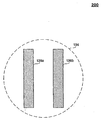
도3에 도시된 것처럼, 본 발명의 일 실시예에 따른 투사 광학계의 출구 퓨필의 블록도가 도시된다. 2개의 레티클 사이의 패턴 정합 목적을 위하여, 출구 퓨필내의 이미지의 위치 변위를 허용하도록 이중 레티클 상의 조명 위치들 사이에 오프셋이 있다. 레티클(104a, 104b)은 "ABCDEFGHIJK"로서 도3에 도시된 것과 같은 패턴을 가진다. 이 패턴은 예시적인 목적을 위한 것이다. 이들 패턴은 출구 퓨필(134)에서 가시적이고, 기판 스테이지(114)상의 패턴의 중첩을 나타낸다.As shown in Fig. 3, a block diagram of an exit pupil of the projection optics according to an embodiment of the present invention is shown. For the purpose of pattern matching between the two reticles, there is an offset between the illumination positions on the double reticle to allow positional displacement of the image in the exit pupil.
일 실시예에서, 2개의 레티클은 동일하다. 그러한 실시예에서, 이미지의 위치에서의 오프셋은 투사 광학계의 축소 비율에 의해 곱해진 출구 퓨필에 있는 이미지 슬릿들의 오프셋과 동일하다. 구체적으로, 레티클(104a, 104b)은 출구 퓨필(134)에서 이미지가 되고, 이미지는 기판 스테이지(114) 상으로 노출된다. 각각의 레티클 이미지로 전달된 노출량은 각각의 조명 슬릿에서 조명 강도를 조정함 으로써 독립적으로 제어될 수 있다.In one embodiment, the two reticles are the same. In such an embodiment, the offset in the position of the image is equal to the offset of the image slits in the exit pupil multiplied by the reduction ratio of the projection optics. Specifically,
본 발명의 일 실시예에서, 이중 레티클(104a, 104b) 각각의 적어도 일부분으로부터의 이미지는 이중 레티클(104a, 104b) 중의 하나의 상이한 위치들로부터의 이미지이다.In one embodiment of the invention, the image from at least a portion of each of the
전술한 것처럼, 교정 검출기(140)는 스캐닝 스테이지(103)로부터 이미지를 수용하도록 기판 스테이지(114) 상에 사용된다. 교정 검출기(140)는 스테이지(103, 114) 사이의 실시간 장치 교정을 허용한다.As discussed above,
본 발명의 일 실시예에서, 기판 스테이지(114)는 레지스트 코팅된 웨이퍼 또는 적어도 하나의 평판 패널 디스플레이와 같은 적어도 하나의 기판을 포함한다.In one embodiment of the invention,
본 발명의 일 실시예에서, 이중 레티클은 집적 회로 패턴의 이미지를 포함한다.In one embodiment of the invention, the dual reticle comprises an image of an integrated circuit pattern.
본 발명의 또 다른 실시예에서, 이중 레티클 중의 하나는 그 레티클로부터 조명된 이미지를 위상 이동하기 위하여 사용된 위상 이동 레티클이다.In another embodiment of the present invention, one of the dual reticles is a phase shift reticle used to phase shift an illuminated image from that reticle.
도4는 본 발명의 일 실시예에 따른 노출 방법의 흐름도를 예시한다. 이중 레티클(104a, 104b)로부터의 이미지로 기판 스테이지 상의 필드를 노출시키는 루틴은 단계(402)에서 시작하여 즉시 단계(406)로 나아간다.4 illustrates a flowchart of an exposure method according to an embodiment of the present invention. The routine of exposing the field on the substrate stage with the image from the
단계(406)에서, 장치(100)는 하나 이상의 레티클을 포함하는 스캐닝 스테이지를 위치 설정한다. 장치는 단계(408)로 나아간다. 다른 실시예에서, 단계(406)후에 그러나 단계(408)전에, 장치(100)는 하나 이상의 레티클로부터 입사하는 비임을 조절한다. 일 실시예에서, 장치(100)는 퓨필 필터로 비임을 조절한다.In
단계(408)에서, 장치(100)는 기판 스테이지 상에 이미지 필드를 위치 설정한다. 기판 스테이지는 웨이퍼와 같은 기판을 포함한다. 장치는 단계(410)로 나아간다.In
단계(410)에서, 장치(100)는 기판 스테이지위에 이미지 필드를 노출시키는 하나 이상의 레티클의 이미지를 스캔한다. 본 발명의 일 실시예에서, 필드는 각각 이중 레티클로부터의 적어도 2개의 이미지로 동시에 노출된다. 선택적으로, 장치는 단계(412)로 나아간다.In
선택적 단계(412)에서, 본 발명의 일 실시예에 따르면, 장치(100)는 기판 스테이지 상의 필드에 이미지를 중첩할 수 있다. 루틴(400)은 그 후 단계(414)로 나아가고 종료된다. 선택적으로, 루틴(400)은 점선 화살표(416)로 도시된 바와 같이 단계(414)에서 단계(402)로 반복될 수 있다. In
도5는 이중 노출 기술을 도시한다. 이중 노출 기술들은 전형적으로 위상경계들에서 도시된 것처럼 간극을 남기는데, 이는 여기의 다른 곳에 기술된 것처럼 문제가 될 수 있다. 도5는 이 어려움을 예시한다. 도5에서, 위상 0 마스크(504)와 위상 180 마스크(508)는 위상경계(506)를 남긴다. 인쇄할 때, 이는 간극(510)이 된다.5 illustrates a double exposure technique. Double exposure techniques typically leave gaps as shown in phase boundaries, which can be problematic as described elsewhere herein. 5 illustrates this difficulty. In FIG. 5, phase 0
도6은 하나 이상의 레티클(또한 플러그/트림 마스크로 불린다)로부터의 추가적인 이미지가 더 우수한 전체 패턴을 제공하는 본 발명의 일 실시예에 따른 이중 노출 기술을 도시한다. 도6을 참조로, 패턴(A)은 위상 0 마스크(604)와 위상 180 마스크(608)를 포함한다. 플러그 또는 트림 패턴(612)의 부가는 간극(510)에서 경험하지 않은 고해상도 패턴(610)을 제공한다.6 illustrates a double exposure technique according to an embodiment of the present invention in which additional images from one or more reticles (also called plug / trim masks) provide a better overall pattern. Referring to FIG. 6, pattern A includes a phase 0
도7은 U-이미지 인쇄를 위해 이중 노출을 사용하는 플러그/트림 마스크/레티클 기술을 도시한다. 도7은 플러그를 갖지 않는 패턴(704)과 트림을 갖는 패턴(706) 사이의 차이에서 지적된 것처럼, 도6에 도시된 것과 같은 플러그 패턴으로 부가적인 이미지(들)를 노출시키는 효과를 보여주는 2개의 사진을 포함한다.7 shows a plug / trim mask / reticle technique using double exposure for U-image printing. FIG. 7 illustrates the effect of exposing additional image (s) with a plug pattern such as that shown in FIG. 6, as indicated in the difference between the
도8은 위상 가장자리 제거를 위한 플러그/트림 마스크의 제2 노출 기술을 도시한다. 도8에서, 위상 가장자리는 도6에 기술되는 것과 같은 플러그 패턴의 사용에 의해서 제거된다. 위상 가장자리(804)는 제거없이 도시되고, 위상 가장자리(806)는 본 발명의 실시예에 따른 플러그 마스크 노출에 의하여 제거된 후 표시된다.8 illustrates a second exposure technique of a plug / trim mask for phase edge removal. In Fig. 8, the phase edge is removed by the use of a plug pattern as described in Fig. 6.
결론conclusion
본 발명의 특정 실시예가 전술되지만, 그들이 단지 예로 제시되었고 제한되지 않는다는 것이 이해되어야 한다. 형태와 상세한 것에서 다양한 변화들은 첨부된 청구의 범위에서 한정된 것처럼 본 발명의 기술 사상과 범위로부터 벗어남이 없이 이루어 질 수 있음이 이 분야에 기술을 가진 사람에 의해서 이해될 것이다. 따라서, 본 발명의 폭과 범위는 전술한 예시적인 실시예 중의 어떤 것에 의하여 제한되지 않아야 하고, 후술하는 청구의 범위와 그 균등물에 따라서만 한정되어야 한다.While specific embodiments of the invention have been described above, it should be understood that they have been presented by way of example only and not limitation. It will be understood by those skilled in the art that various changes in form and detail may be made without departing from the spirit and scope of the invention as defined in the appended claims. Accordingly, the breadth and scope of the present invention should not be limited by any of the above-described exemplary embodiments, but should be defined only in accordance with the following claims and their equivalents.
Claims (14)
Applications Claiming Priority (3)
| Application Number | Priority Date | Filing Date | Title |
|---|---|---|---|
| US27138001P | 2001-02-27 | 2001-02-27 | |
| US60/271,380 | 2001-02-27 | ||
| PCT/US2002/005656 WO2002069049A2 (en) | 2001-02-27 | 2002-02-27 | Simultaneous imaging of two reticles |
Publications (2)
| Publication Number | Publication Date |
|---|---|
| KR20030053473A KR20030053473A (en) | 2003-06-28 |
| KR100815222B1 true KR100815222B1 (en) | 2008-03-19 |
Family
ID=23035311
Family Applications (1)
| Application Number | Title | Priority Date | Filing Date |
|---|---|---|---|
| KR1020027014433A Expired - Fee Related KR100815222B1 (en) | 2001-02-27 | 2002-02-27 | A method of exposing a field on a substrate stage with an image from a lithographic apparatus and at least two patterns formed on at least one reticle |
Country Status (5)
| Country | Link |
|---|---|
| US (1) | US6611316B2 (en) |
| EP (1) | EP1364257A1 (en) |
| JP (1) | JP4714403B2 (en) |
| KR (1) | KR100815222B1 (en) |
| WO (1) | WO2002069049A2 (en) |
Families Citing this family (301)
| Publication number | Priority date | Publication date | Assignee | Title |
|---|---|---|---|---|
| EP1255162A1 (en) | 2001-05-04 | 2002-11-06 | ASML Netherlands B.V. | Lithographic apparatus |
| US6795168B2 (en) * | 2002-04-08 | 2004-09-21 | Numerical Technologies, Inc. | Method and apparatus for exposing a wafer using multiple masks during an integrated circuit manufacturing process |
| KR101503992B1 (en) | 2003-04-09 | 2015-03-18 | 가부시키가이샤 니콘 | Exposure method and apparatus, and device manufacturing method |
| TWI511179B (en) | 2003-10-28 | 2015-12-01 | 尼康股份有限公司 | Optical illumination device, exposure device, exposure method and device manufacturing method |
| TWI512335B (en) | 2003-11-20 | 2015-12-11 | 尼康股份有限公司 | Beam conversion element, optical illumination device, exposure device, and exposure method |
| US7361457B2 (en) * | 2004-01-13 | 2008-04-22 | International Business Machines Corporation | Real-time configurable masking |
| KR101135232B1 (en) * | 2004-01-20 | 2012-04-12 | 칼 짜이스 에스엠테 게엠베하 | Microlithographic projection exposure apparatus |
| US7064078B2 (en) * | 2004-01-30 | 2006-06-20 | Applied Materials | Techniques for the use of amorphous carbon (APF) for various etch and litho integration scheme |
| WO2005076324A1 (en) | 2004-02-04 | 2005-08-18 | Nikon Corporation | Exposure apparatus, exposure method, and device producing method |
| TWI379344B (en) | 2004-02-06 | 2012-12-11 | Nikon Corp | Polarization changing device, optical illumination apparatus, light-exposure apparatus and light-exposure method |
| US20070030467A1 (en) * | 2004-02-19 | 2007-02-08 | Nikon Corporation | Exposure apparatus, exposure method, and device fabricating method |
| DE102004013886A1 (en) | 2004-03-16 | 2005-10-06 | Carl Zeiss Smt Ag | Multiple Exposure Method, Microlithography Projection Exposure System and Projection System |
| US7387871B2 (en) * | 2004-08-26 | 2008-06-17 | Seagate Technology Llc | Mask complementary multiple exposure technique |
| US20070258068A1 (en) * | 2005-02-17 | 2007-11-08 | Hiroto Horikawa | Exposure Apparatus, Exposure Method, and Device Fabricating Method |
| US8638422B2 (en) | 2005-03-18 | 2014-01-28 | Nikon Corporation | Exposure method, exposure apparatus, method for producing device, and method for evaluating exposure apparatus |
| JP2006267761A (en) * | 2005-03-25 | 2006-10-05 | Fujitsu Hitachi Plasma Display Ltd | Glass photomask exposure method |
| WO2006106833A1 (en) * | 2005-03-30 | 2006-10-12 | Nikon Corporation | Exposure apparatus, exposure method, and device producing method |
| US9239524B2 (en) * | 2005-03-30 | 2016-01-19 | Nikon Corporation | Exposure condition determination method, exposure method, exposure apparatus, and device manufacturing method involving detection of the situation of a liquid immersion region |
| US7209217B2 (en) * | 2005-04-08 | 2007-04-24 | Asml Netherlands B.V. | Lithographic apparatus and device manufacturing method utilizing plural patterning devices |
| WO2006112436A1 (en) | 2005-04-18 | 2006-10-26 | Nikon Corporation | Exposure device, exposure method, and device manufacturing method |
| KR101479392B1 (en) | 2005-04-28 | 2015-01-05 | 가부시키가이샤 니콘 | Exposure method, exposure apparatus and device manufacturing method |
| KR101452145B1 (en) | 2005-05-12 | 2014-10-16 | 가부시키가이샤 니콘 | Projection optical system, exposure apparatus and exposure method |
| US7736825B2 (en) * | 2005-06-02 | 2010-06-15 | Asml Holding N.V. | Lithographic apparatus and device manufacturing method utilizing a resettable or reversible contrast enhancing layer in a multiple exposure system |
| US20070085989A1 (en) * | 2005-06-21 | 2007-04-19 | Nikon Corporation | Exposure apparatus and exposure method, maintenance method, and device manufacturing method |
| WO2006137410A1 (en) | 2005-06-21 | 2006-12-28 | Nikon Corporation | Exposure apparatus, exposure method, maintenance method and device manufacturing method |
| US7924416B2 (en) * | 2005-06-22 | 2011-04-12 | Nikon Corporation | Measurement apparatus, exposure apparatus, and device manufacturing method |
| US20090033896A1 (en) * | 2005-06-28 | 2009-02-05 | Hiroyuki Nagasaka | Exposure apparatus and method, and device manufacturing method |
| KR100613461B1 (en) * | 2005-06-29 | 2006-08-17 | 주식회사 하이닉스반도체 | Dual exposure method using double exposure technology and photomask for it |
| US20090033890A1 (en) * | 2005-06-29 | 2009-02-05 | Nikon Corporation | Exposure apparatus, substrate processing method, and device producing method |
| JP5194792B2 (en) * | 2005-06-30 | 2013-05-08 | 株式会社ニコン | Exposure apparatus and method, exposure apparatus maintenance method, and device manufacturing method |
| WO2007004567A1 (en) | 2005-07-01 | 2007-01-11 | Nikon Corporation | Exposure apparatus, exposure method, device manufacturing method, and system |
| KR20080031376A (en) * | 2005-07-11 | 2008-04-08 | 가부시키가이샤 니콘 | Exposure apparatus and device manufacturing method |
| KR100729263B1 (en) * | 2005-07-14 | 2007-06-15 | 삼성전자주식회사 | Substrate exposure apparatus |
| JP5309565B2 (en) * | 2005-08-05 | 2013-10-09 | 株式会社ニコン | Stage apparatus, exposure apparatus, method, exposure method, and device manufacturing method |
| TWI430039B (en) | 2005-08-23 | 2014-03-11 | 尼康股份有限公司 | An exposure apparatus and an exposure method, and an element manufacturing method |
| TWI450044B (en) | 2005-08-31 | 2014-08-21 | 尼康股份有限公司 | An optical element, an exposure apparatus using the same, an exposure method, and a manufacturing method of the micro-element |
| KR101388345B1 (en) * | 2005-09-09 | 2014-04-22 | 가부시키가이샤 니콘 | Exposure apparatus, exposure method, and device production method |
| US8111374B2 (en) | 2005-09-09 | 2012-02-07 | Nikon Corporation | Analysis method, exposure method, and device manufacturing method |
| WO2007034838A1 (en) | 2005-09-21 | 2007-03-29 | Nikon Corporation | Exposure device, exposure method, and device fabrication method |
| US20070070323A1 (en) * | 2005-09-21 | 2007-03-29 | Nikon Corporation | Exposure apparatus, exposure method, and device fabricating method |
| JPWO2007043535A1 (en) * | 2005-10-07 | 2009-04-16 | 株式会社ニコン | Optical characteristic measuring method, exposure method, device manufacturing method, inspection apparatus and measuring method |
| US7948675B2 (en) * | 2005-10-11 | 2011-05-24 | Nikon Corporation | Surface-corrected multilayer-film mirrors with protected reflective surfaces, exposure systems comprising same, and associated methods |
| US20070095739A1 (en) * | 2005-10-24 | 2007-05-03 | Nikon Corporation | Utility transfer apparatus, stage apparatus, exposure apparatus, and device manufacturing method |
| US8681314B2 (en) * | 2005-10-24 | 2014-03-25 | Nikon Corporation | Stage device and coordinate correction method for the same, exposure apparatus, and device manufacturing method |
| US20070127135A1 (en) * | 2005-11-01 | 2007-06-07 | Nikon Corporation | Exposure apparatus, exposure method and device manufacturing method |
| EP1950795A4 (en) | 2005-11-01 | 2010-06-02 | Nikon Corp | Exposure apparatus, exposure method and device manufacturing method |
| US20070127002A1 (en) * | 2005-11-09 | 2007-06-07 | Nikon Corporation | Exposure apparatus and method, and device manufacturing method |
| KR20080066836A (en) * | 2005-11-09 | 2008-07-16 | 가부시키가이샤 니콘 | Exposure apparatus, exposure method, and device manufacturing method |
| WO2007055199A1 (en) | 2005-11-09 | 2007-05-18 | Nikon Corporation | Exposure apparatus and method, and method for manufacturing device |
| WO2007055373A1 (en) | 2005-11-14 | 2007-05-18 | Nikon Corporation | Liquid recovery member, exposure apparatus, exposure method, and device production method |
| KR20080068006A (en) * | 2005-11-15 | 2008-07-22 | 가부시키가이샤 니콘 | Exposure apparatus, exposure method, and device manufacturing method |
| EP1953806A1 (en) | 2005-11-16 | 2008-08-06 | Nikon Corporation | Substrate processing method, photomask manufacturing method, photomask and device manufacturing method |
| US7803516B2 (en) | 2005-11-21 | 2010-09-28 | Nikon Corporation | Exposure method, device manufacturing method using the same, exposure apparatus, and substrate processing method and apparatus |
| JP2007165869A (en) | 2005-11-21 | 2007-06-28 | Nikon Corp | Exposure method, device manufacturing method using the same, exposure apparatus, and substrate processing method and apparatus |
| JP2007318069A (en) * | 2005-12-06 | 2007-12-06 | Nikon Corp | Exposure apparatus and exposure method, device manufacturing method, and projection optical system |
| KR20080071552A (en) * | 2005-12-06 | 2008-08-04 | 가부시키가이샤 니콘 | Exposure method, exposure apparatus and device manufacturing method |
| WO2007066679A1 (en) * | 2005-12-06 | 2007-06-14 | Nikon Corporation | Exposure apparatus, exposure method, projection optical system and device manufacturing method |
| US7782442B2 (en) | 2005-12-06 | 2010-08-24 | Nikon Corporation | Exposure apparatus, exposure method, projection optical system and device producing method |
| TWI406321B (en) | 2005-12-08 | 2013-08-21 | 尼康股份有限公司 | A substrate holding device, an exposure apparatus, an exposure method, and an element manufacturing method |
| KR100689836B1 (en) * | 2005-12-23 | 2007-03-08 | 삼성전자주식회사 | Exposure equipment having an auxiliary photo mask and exposure method using the same |
| CN102636966B (en) | 2005-12-28 | 2014-12-03 | 株式会社尼康 | Exposure method and exposure apparatus, and device manufacturing method |
| US8953148B2 (en) | 2005-12-28 | 2015-02-10 | Nikon Corporation | Exposure apparatus and making method thereof |
| JP2007201457A (en) * | 2005-12-28 | 2007-08-09 | Nikon Corp | Exposure apparatus, exposure method, and device manufacturing method |
| US8411271B2 (en) | 2005-12-28 | 2013-04-02 | Nikon Corporation | Pattern forming method, pattern forming apparatus, and device manufacturing method |
| KR20080088579A (en) * | 2005-12-28 | 2008-10-02 | 가부시키가이샤 니콘 | Exposure apparatus, exposure method, device manufacturing method |
| WO2007077925A1 (en) | 2005-12-28 | 2007-07-12 | Nikon Corporation | Pattern formation method, pattern formation device, and device fabrication method |
| TWI605491B (en) | 2006-01-19 | 2017-11-11 | 尼康股份有限公司 | Exposure apparatus and exposure method, and component manufacturing method |
| EP1986224A4 (en) * | 2006-02-16 | 2012-01-25 | Nikon Corp | Exposure apparatus, exposing method, and device manufacturing method |
| TW200801833A (en) * | 2006-02-16 | 2008-01-01 | Nikon Corp | Exposure apparatus, exposure method and device manufacturing method |
| KR20080102192A (en) * | 2006-02-16 | 2008-11-24 | 가부시키가이샤 니콘 | Exposure apparatus, exposure method, and device manufacturing method |
| JP4957281B2 (en) * | 2006-02-16 | 2012-06-20 | 株式会社ニコン | Exposure apparatus, exposure method, and device manufacturing method |
| EP1986222A4 (en) * | 2006-02-16 | 2010-09-01 | Nikon Corp | Exposure apparatus, exposing method, and device manufacturing method |
| KR101346581B1 (en) | 2006-02-21 | 2014-01-02 | 가부시키가이샤 니콘 | Pattern forming apparatus, pattern forming method, mobile object driving system, mobile body driving method, exposure apparatus, exposure method and device manufacturing method |
| SG178816A1 (en) | 2006-02-21 | 2012-03-29 | Nikon Corp | Measuring apparatus and method, processing apparatus and method, pattern forming apparatus and method, exposure appararus and method, and device manufacturing method |
| KR101495471B1 (en) | 2006-02-21 | 2015-02-23 | 가부시키가이샤 니콘 | Pattern forming apparatus, mark detecting apparatus, exposure apparatus, pattern forming method, exposure method and device manufacturing method |
| US8023103B2 (en) | 2006-03-03 | 2011-09-20 | Nikon Corporation | Exposure apparatus, exposure method, and method for producing device |
| JP4929762B2 (en) * | 2006-03-03 | 2012-05-09 | 株式会社ニコン | Exposure apparatus, exposure method, and device manufacturing method |
| EP1993121A4 (en) * | 2006-03-03 | 2011-12-07 | Nikon Corp | Exposure apparatus and device manufacturing method |
| WO2007105645A1 (en) | 2006-03-13 | 2007-09-20 | Nikon Corporation | Exposure apparatus, maintenance method, exposure method and device manufacturing method |
| US8982322B2 (en) | 2006-03-17 | 2015-03-17 | Nikon Corporation | Exposure apparatus and device manufacturing method |
| US20080013062A1 (en) * | 2006-03-23 | 2008-01-17 | Nikon Corporation | Exposure apparatus, exposure method, and device manufacturing method |
| TWI454859B (en) | 2006-03-30 | 2014-10-01 | 尼康股份有限公司 | Mobile device, exposure device and exposure method, and component manufacturing method |
| US7884921B2 (en) * | 2006-04-12 | 2011-02-08 | Nikon Corporation | Illumination optical apparatus, projection exposure apparatus, projection optical system, and device manufacturing method |
| CN101379593A (en) * | 2006-04-14 | 2009-03-04 | 株式会社尼康 | Exposure device, device-manufacturing method and exposing method |
| KR101486589B1 (en) | 2006-04-17 | 2015-01-26 | 가부시키가이샤 니콘 | Illuminating optical apparatus, exposure apparatus and device manufacturing method |
| DE102006021797A1 (en) | 2006-05-09 | 2007-11-15 | Carl Zeiss Smt Ag | Optical imaging device with thermal damping |
| SG175671A1 (en) | 2006-05-18 | 2011-11-28 | Nikon Corp | Exposure method and apparatus, maintenance method and device manufacturing method |
| TW200818256A (en) | 2006-05-22 | 2008-04-16 | Nikon Corp | Exposure method and apparatus, maintenance method, and device manufacturing method |
| WO2007136089A1 (en) | 2006-05-23 | 2007-11-29 | Nikon Corporation | Maintenance method, exposure method and apparatus, and device manufacturing method |
| KR20090026139A (en) | 2006-05-24 | 2009-03-11 | 가부시키가이샤 니콘 | Retention device and exposure device |
| WO2007139017A1 (en) * | 2006-05-29 | 2007-12-06 | Nikon Corporation | Liquid recovery member, substrate holding member, exposure apparatus and device manufacturing method |
| JPWO2007142350A1 (en) | 2006-06-09 | 2009-10-29 | 株式会社ニコン | Pattern forming method and pattern forming apparatus, exposure method and exposure apparatus, and device manufacturing method |
| JPWO2007142351A1 (en) | 2006-06-09 | 2009-10-29 | 株式会社ニコン | MOBILE DEVICE, EXPOSURE APPARATUS, EXPOSURE METHOD, AND DEVICE MANUFACTURING METHOD |
| WO2008001871A1 (en) | 2006-06-30 | 2008-01-03 | Nikon Corporation | Maintenance method, exposure method and apparatus and device manufacturing method |
| WO2008007633A1 (en) * | 2006-07-12 | 2008-01-17 | Nikon Corporation | Illuminating optical apparatus, exposure apparatus and device manufacturing method |
| JP5151981B2 (en) | 2006-08-30 | 2013-02-27 | 株式会社ニコン | Exposure apparatus and device manufacturing method |
| EP3418807A1 (en) | 2006-08-31 | 2018-12-26 | Nikon Corporation | Exposure apparatus, exposure method, and device manufacturing method |
| TWI655517B (en) | 2006-08-31 | 2019-04-01 | 日商尼康股份有限公司 | Exposure apparatus and method, and component manufacturing method |
| KR101634893B1 (en) | 2006-08-31 | 2016-06-29 | 가부시키가이샤 니콘 | Mobile body drive method and mobile body drive system, pattern formation method and apparatus, exposure method and apparatus, and device manufacturing method |
| TWI623825B (en) | 2006-09-01 | 2018-05-11 | Nikon Corporation | Exposure device and method, and element manufacturing method |
| TWI434326B (en) * | 2006-09-01 | 2014-04-11 | 尼康股份有限公司 | Mobile body driving method and moving body driving system, pattern forming method and apparatus, exposure method and apparatus, component manufacturing method, and correcting method |
| TWI457723B (en) | 2006-09-08 | 2014-10-21 | 尼康股份有限公司 | A mask, an exposure device, and an element manufacturing method |
| JP5029611B2 (en) * | 2006-09-08 | 2012-09-19 | 株式会社ニコン | Cleaning member, cleaning method, exposure apparatus, and device manufacturing method |
| US7872730B2 (en) | 2006-09-15 | 2011-01-18 | Nikon Corporation | Immersion exposure apparatus and immersion exposure method, and device manufacturing method |
| JPWO2008038751A1 (en) | 2006-09-28 | 2010-01-28 | 株式会社ニコン | Line width measurement method, image formation state detection method, adjustment method, exposure method, and device manufacturing method |
| US7999918B2 (en) * | 2006-09-29 | 2011-08-16 | Nikon Corporation | Movable body system, pattern formation apparatus, exposure apparatus and exposure method, and device manufacturing method |
| KR101419196B1 (en) | 2006-09-29 | 2014-07-15 | 가부시키가이샤 니콘 | Exposure apparatus, exposure method, and device manufacturing method |
| US20080100909A1 (en) * | 2006-10-30 | 2008-05-01 | Nikon Corporation | Optical element, liquid immersion exposure apparatus, liquid immersion exposure method, and method for producing microdevice |
| KR101549709B1 (en) | 2006-11-09 | 2015-09-11 | 가부시키가이샤 니콘 | Holding unit position detecting system and exposure system moving method position detecting method exposure method adjusting method of detection system and device producing method |
| JP5055971B2 (en) | 2006-11-16 | 2012-10-24 | 株式会社ニコン | Surface treatment method, surface treatment apparatus, exposure method, exposure apparatus, and device manufacturing method |
| US20080156356A1 (en) | 2006-12-05 | 2008-07-03 | Nikon Corporation | Cleaning liquid, cleaning method, liquid generating apparatus, exposure apparatus, and device fabricating method |
| KR20090106555A (en) | 2006-12-27 | 2009-10-09 | 가부시키가이샤 니콘 | Stage apparatus, exposure apparatus and device manufacturing method |
| US20080212047A1 (en) * | 2006-12-28 | 2008-09-04 | Nikon Corporation | Exposure apparatus, exposing method, and device fabricating method |
| US8004651B2 (en) | 2007-01-23 | 2011-08-23 | Nikon Corporation | Liquid recovery system, immersion exposure apparatus, immersion exposing method, and device fabricating method |
| WO2008108253A2 (en) * | 2007-02-23 | 2008-09-12 | Nikon Corporation | Exposing method, exposure apparatus, device fabricating method, and substrate for immersion exposure |
| US8323855B2 (en) | 2007-03-01 | 2012-12-04 | Nikon Corporation | Pellicle frame apparatus, mask, exposing method, exposure apparatus, and device fabricating method |
| US8497980B2 (en) * | 2007-03-19 | 2013-07-30 | Nikon Corporation | Holding apparatus, exposure apparatus, exposure method, and device manufacturing method |
| US8134685B2 (en) | 2007-03-23 | 2012-03-13 | Nikon Corporation | Liquid recovery system, immersion exposure apparatus, immersion exposing method, and device fabricating method |
| US20080246941A1 (en) * | 2007-04-06 | 2008-10-09 | Katsura Otaki | Wavefront aberration measuring device, projection exposure apparatus, method for manufacturing projection optical system, and method for manufacturing device |
| JPWO2008132799A1 (en) * | 2007-04-12 | 2010-07-22 | 株式会社ニコン | Measuring method, exposure method, and device manufacturing method |
| US8665418B2 (en) * | 2007-04-18 | 2014-03-04 | Nikon Corporation | Projection optical system, exposure apparatus, and device manufacturing method |
| US8194322B2 (en) * | 2007-04-23 | 2012-06-05 | Nikon Corporation | Multilayer-film reflective mirror, exposure apparatus, device manufacturing method, and manufacturing method of multilayer-film reflective mirror |
| US20080266651A1 (en) * | 2007-04-24 | 2008-10-30 | Katsuhiko Murakami | Optical apparatus, multilayer-film reflective mirror, exposure apparatus, and device |
| US8300207B2 (en) | 2007-05-17 | 2012-10-30 | Nikon Corporation | Exposure apparatus, immersion system, exposing method, and device fabricating method |
| US20090122282A1 (en) * | 2007-05-21 | 2009-05-14 | Nikon Corporation | Exposure apparatus, liquid immersion system, exposing method, and device fabricating method |
| WO2008146819A1 (en) * | 2007-05-28 | 2008-12-04 | Nikon Corporation | Exposure apparatus, device manufacturing method, cleaning device, cleaning method and exposure method |
| US8164736B2 (en) * | 2007-05-29 | 2012-04-24 | Nikon Corporation | Exposure method, exposure apparatus, and method for producing device |
| US8098362B2 (en) * | 2007-05-30 | 2012-01-17 | Nikon Corporation | Detection device, movable body apparatus, pattern formation apparatus and pattern formation method, exposure apparatus and exposure method, and device manufacturing method |
| WO2008149853A1 (en) * | 2007-06-04 | 2008-12-11 | Nikon Corporation | Environment control apparatus, stage apparatus, exposure apparatus, and device production method |
| WO2008153023A1 (en) * | 2007-06-11 | 2008-12-18 | Nikon Corporation | Measuring member, sensor, measuring method, exposure apparatus, exposure method, and device producing method |
| US8264669B2 (en) | 2007-07-24 | 2012-09-11 | Nikon Corporation | Movable body drive method, pattern formation method, exposure method, and device manufacturing method for maintaining position coordinate before and after switching encoder head |
| WO2009013905A1 (en) | 2007-07-24 | 2009-01-29 | Nikon Corporation | Position measuring system, exposure device, position measuring method, exposure method, device manufacturing method, tool, and measuring method |
| US8547527B2 (en) * | 2007-07-24 | 2013-10-01 | Nikon Corporation | Movable body drive method and movable body drive system, pattern formation method and pattern formation apparatus, and device manufacturing method |
| US8194232B2 (en) | 2007-07-24 | 2012-06-05 | Nikon Corporation | Movable body drive method and movable body drive system, pattern formation method and apparatus, exposure method and apparatus, position control method and position control system, and device manufacturing method |
| US9025126B2 (en) * | 2007-07-31 | 2015-05-05 | Nikon Corporation | Exposure apparatus adjusting method, exposure apparatus, and device fabricating method |
| US8867022B2 (en) | 2007-08-24 | 2014-10-21 | Nikon Corporation | Movable body drive method and movable body drive system, pattern formation method and apparatus, and device manufacturing method |
| US8237919B2 (en) | 2007-08-24 | 2012-08-07 | Nikon Corporation | Movable body drive method and movable body drive system, pattern formation method and apparatus, exposure method and apparatus, and device manufacturing method for continuous position measurement of movable body before and after switching between sensor heads |
| US8023106B2 (en) | 2007-08-24 | 2011-09-20 | Nikon Corporation | Movable body drive method and movable body drive system, pattern formation method and apparatus, exposure method and apparatus, and device manufacturing method |
| US8218129B2 (en) * | 2007-08-24 | 2012-07-10 | Nikon Corporation | Movable body drive method and movable body drive system, pattern formation method and apparatus, exposure method and apparatus, device manufacturing method, measuring method, and position measurement system |
| US20090051895A1 (en) * | 2007-08-24 | 2009-02-26 | Nikon Corporation | Movable body drive method and movable body drive system, pattern formation method and apparatus, device manufacturing method, and processing system |
| US9304412B2 (en) | 2007-08-24 | 2016-04-05 | Nikon Corporation | Movable body drive method and movable body drive system, pattern formation method and apparatus, exposure method and apparatus, device manufacturing method, and measuring method |
| CN101855705A (en) * | 2007-09-07 | 2010-10-06 | 国立大学法人横滨国立大学 | Drive control method, drive control device, stage control method, stage control device, exposure method, exposure device, and measurement device |
| US8421994B2 (en) * | 2007-09-27 | 2013-04-16 | Nikon Corporation | Exposure apparatus |
| JP5267029B2 (en) | 2007-10-12 | 2013-08-21 | 株式会社ニコン | Illumination optical apparatus, exposure apparatus, and device manufacturing method |
| EP2179329A1 (en) | 2007-10-16 | 2010-04-28 | Nikon Corporation | Illumination optical system, exposure apparatus, and device manufacturing method |
| EP2179330A1 (en) | 2007-10-16 | 2010-04-28 | Nikon Corporation | Illumination optical system, exposure apparatus, and device manufacturing method |
| US8279399B2 (en) | 2007-10-22 | 2012-10-02 | Nikon Corporation | Exposure apparatus, exposure method, and device manufacturing method |
| DE102007051669A1 (en) * | 2007-10-26 | 2009-04-30 | Carl Zeiss Smt Ag | Imaging optics, projection exposure apparatus for microlithography with such an imaging optical system and method for producing a microstructured component with such a projection exposure apparatus |
| US9013681B2 (en) * | 2007-11-06 | 2015-04-21 | Nikon Corporation | Movable body apparatus, pattern formation apparatus and exposure apparatus, and device manufacturing method |
| US9116346B2 (en) | 2007-11-06 | 2015-08-25 | Nikon Corporation | Illumination apparatus, illumination method, exposure apparatus, and device manufacturing method |
| US9256140B2 (en) * | 2007-11-07 | 2016-02-09 | Nikon Corporation | Movable body apparatus, pattern formation apparatus and exposure apparatus, and device manufacturing method with measurement device to measure movable body in Z direction |
| CN101675500B (en) * | 2007-11-07 | 2011-05-18 | 株式会社尼康 | Exposure apparatus, exposure method and device manufacturing method |
| US8665455B2 (en) * | 2007-11-08 | 2014-03-04 | Nikon Corporation | Movable body apparatus, pattern formation apparatus and exposure apparatus, and device manufacturing method |
| US8422015B2 (en) * | 2007-11-09 | 2013-04-16 | Nikon Corporation | Movable body apparatus, pattern formation apparatus and exposure apparatus, and device manufacturing method |
| US20090147228A1 (en) * | 2007-12-11 | 2009-06-11 | Nikon Corporation | Exposure apparatus, manufacturing method thereof, and maintenance method of exposure apparatus |
| JP5403263B2 (en) * | 2007-12-11 | 2014-01-29 | 株式会社ニコン | MOBILE DEVICE, EXPOSURE APPARATUS, PATTERN FORMING APPARATUS, AND DEVICE MANUFACTURING METHOD |
| US8115906B2 (en) * | 2007-12-14 | 2012-02-14 | Nikon Corporation | Movable body system, pattern formation apparatus, exposure apparatus and measurement device, and device manufacturing method |
| US8711327B2 (en) * | 2007-12-14 | 2014-04-29 | Nikon Corporation | Exposure apparatus, exposure method, and device manufacturing method |
| US8355113B2 (en) * | 2007-12-17 | 2013-01-15 | Nikon Corporation | Exposure apparatus, exposure method and device manufacturing method |
| US20090174873A1 (en) * | 2007-12-17 | 2009-07-09 | Nikon Corporation | Exposure apparatus, exposure method and device manufacturing method |
| SG183058A1 (en) * | 2007-12-17 | 2012-08-30 | Nikon Corp | Exposure apparatus, exposure method and device manufacturing method |
| US8964166B2 (en) * | 2007-12-17 | 2015-02-24 | Nikon Corporation | Stage device, exposure apparatus and method of producing device |
| SG153748A1 (en) * | 2007-12-17 | 2009-07-29 | Asml Holding Nv | Lithographic method and apparatus |
| US8451425B2 (en) * | 2007-12-28 | 2013-05-28 | Nikon Corporation | Exposure apparatus, exposure method, cleaning apparatus, and device manufacturing method |
| US8792079B2 (en) * | 2007-12-28 | 2014-07-29 | Nikon Corporation | Exposure apparatus, exposure method, and device manufacturing method having encoders to measure displacement between optical member and measurement mount and between measurement mount and movable body |
| US8237916B2 (en) * | 2007-12-28 | 2012-08-07 | Nikon Corporation | Movable body drive system, pattern formation apparatus, exposure apparatus and exposure method, and device manufacturing method |
| TWI643035B (en) | 2007-12-28 | 2018-12-01 | 日商尼康股份有限公司 | Exposure apparatus, exposure method, and component manufacturing method |
| US8269945B2 (en) * | 2007-12-28 | 2012-09-18 | Nikon Corporation | Movable body drive method and apparatus, exposure method and apparatus, pattern formation method and apparatus, and device manufacturing method |
| JP5369443B2 (en) | 2008-02-05 | 2013-12-18 | 株式会社ニコン | Stage apparatus, exposure apparatus, exposure method, and device manufacturing method |
| KR20100124245A (en) * | 2008-02-08 | 2010-11-26 | 가부시키가이샤 니콘 | Position measuring system and position measuring method, mobile body device, mobile body driving method, exposure device and exposure method, pattern forming device, and device manufacturing method |
| US20090218743A1 (en) * | 2008-02-29 | 2009-09-03 | Nikon Corporation | Substrate holding apparatus, exposure apparatus, exposing method, device fabricating method, plate member, and wall |
| US20100039628A1 (en) * | 2008-03-19 | 2010-02-18 | Nikon Corporation | Cleaning tool, cleaning method, and device fabricating method |
| US8233139B2 (en) * | 2008-03-27 | 2012-07-31 | Nikon Corporation | Immersion system, exposure apparatus, exposing method, and device fabricating method |
| SG156564A1 (en) * | 2008-04-09 | 2009-11-26 | Asml Holding Nv | Lithographic apparatus and device manufacturing method |
| TW200947149A (en) * | 2008-04-11 | 2009-11-16 | Nikon Corp | Stage device, exposure device and device production method |
| US8654306B2 (en) * | 2008-04-14 | 2014-02-18 | Nikon Corporation | Exposure apparatus, cleaning method, and device fabricating method |
| JP5472101B2 (en) * | 2008-04-30 | 2014-04-16 | 株式会社ニコン | Exposure apparatus and device manufacturing method |
| EP2284865B1 (en) | 2008-04-30 | 2015-09-02 | Nikon Corporation | Stage apparatus, patterning apparatus, exposure apparatus, stage drive apparatus, exposure method, and device fabrication method |
| US8228482B2 (en) * | 2008-05-13 | 2012-07-24 | Nikon Corporation | Exposure apparatus, exposure method, and device manufacturing method |
| US8817236B2 (en) | 2008-05-13 | 2014-08-26 | Nikon Corporation | Movable body system, movable body drive method, pattern formation apparatus, pattern formation method, exposure apparatus, exposure method, and device manufacturing method |
| US8786829B2 (en) * | 2008-05-13 | 2014-07-22 | Nikon Corporation | Exposure apparatus, exposure method, and device manufacturing method |
| CN105606344B (en) | 2008-05-28 | 2019-07-30 | 株式会社尼康 | Illumination optical system, illumination method, exposure device, and exposure method |
| US20090305171A1 (en) * | 2008-06-10 | 2009-12-10 | Nikon Corporation | Apparatus for scanning sites on a wafer along a short dimension of the sites |
| WO2010005081A1 (en) * | 2008-07-10 | 2010-01-14 | 株式会社ニコン | Deformation measuring apparatus, exposure apparatus, jig for deformation measuring apparatus, position measuring method and device manufacturing method |
| TW201009895A (en) * | 2008-08-11 | 2010-03-01 | Nikon Corp | Exposure apparatus, maintaining method and device fabricating method |
| US8736813B2 (en) * | 2008-08-26 | 2014-05-27 | Nikon Corporation | Exposure apparatus with an illumination system generating multiple illumination beams |
| US8705170B2 (en) * | 2008-08-29 | 2014-04-22 | Nikon Corporation | High NA catadioptric imaging optics for imaging A reticle to a pair of imaging locations |
| US9304385B2 (en) * | 2008-09-16 | 2016-04-05 | Nikon Corporation | Exposure method and device manufacturing method including selective deformation of a mask |
| US8508735B2 (en) | 2008-09-22 | 2013-08-13 | Nikon Corporation | Movable body apparatus, movable body drive method, exposure apparatus, exposure method, and device manufacturing method |
| US8994923B2 (en) * | 2008-09-22 | 2015-03-31 | Nikon Corporation | Movable body apparatus, exposure apparatus, exposure method, and device manufacturing method |
| US8325325B2 (en) | 2008-09-22 | 2012-12-04 | Nikon Corporation | Movable body apparatus, movable body drive method, exposure apparatus, exposure method, and device manufacturing method |
| US8384875B2 (en) * | 2008-09-29 | 2013-02-26 | Nikon Corporation | Exposure apparatus, exposure method, and method for producing device |
| US20100091257A1 (en) * | 2008-10-10 | 2010-04-15 | Nikon Corporation | Optical Imaging System and Method for Imaging Up to Four Reticles to a Single Imaging Location |
| US20100123883A1 (en) * | 2008-11-17 | 2010-05-20 | Nikon Corporation | Projection optical system, exposure apparatus, and device manufacturing method |
| JP5151949B2 (en) * | 2008-12-10 | 2013-02-27 | 株式会社ニコン | MOBILE DEVICE, MOBILE DRIVING METHOD, EXPOSURE APPARATUS, AND DEVICE MANUFACTURING METHOD |
| US8902402B2 (en) | 2008-12-19 | 2014-12-02 | Nikon Corporation | Movable body apparatus, exposure apparatus, exposure method, and device manufacturing method |
| US8599359B2 (en) | 2008-12-19 | 2013-12-03 | Nikon Corporation | Exposure apparatus, exposure method, device manufacturing method, and carrier method |
| US8773635B2 (en) * | 2008-12-19 | 2014-07-08 | Nikon Corporation | Exposure apparatus, exposure method, and device manufacturing method |
| US8760629B2 (en) * | 2008-12-19 | 2014-06-24 | Nikon Corporation | Exposure apparatus including positional measurement system of movable body, exposure method of exposing object including measuring positional information of movable body, and device manufacturing method that includes exposure method of exposing object, including measuring positional information of movable body |
| US8896806B2 (en) * | 2008-12-29 | 2014-11-25 | Nikon Corporation | Exposure apparatus, exposure method, and device manufacturing method |
| US20100196832A1 (en) * | 2009-01-30 | 2010-08-05 | Nikon Corporation | Exposure apparatus, exposing method, liquid immersion member and device fabricating method |
| JP5482784B2 (en) | 2009-03-10 | 2014-05-07 | 株式会社ニコン | Exposure apparatus, exposure method, and device manufacturing method |
| US8953143B2 (en) * | 2009-04-24 | 2015-02-10 | Nikon Corporation | Liquid immersion member |
| US20100296074A1 (en) * | 2009-04-30 | 2010-11-25 | Nikon Corporation | Exposure method, and device manufacturing method |
| US20110085152A1 (en) * | 2009-05-07 | 2011-04-14 | Hideaki Nishino | Vibration control apparatus, vibration control method, exposure apparatus, and device manufacturing method |
| US20100323303A1 (en) * | 2009-05-15 | 2010-12-23 | Nikon Corporation | Liquid immersion member, exposure apparatus, exposing method, and device fabricating method |
| JPWO2010131490A1 (en) * | 2009-05-15 | 2012-11-01 | 株式会社ニコン | Exposure apparatus and device manufacturing method |
| US8970820B2 (en) | 2009-05-20 | 2015-03-03 | Nikon Corporation | Object exchange method, exposure method, carrier system, exposure apparatus, and device manufacturing method |
| US8792084B2 (en) * | 2009-05-20 | 2014-07-29 | Nikon Corporation | Exposure apparatus, exposure method, and device manufacturing method |
| US8553204B2 (en) | 2009-05-20 | 2013-10-08 | Nikon Corporation | Movable body apparatus, exposure apparatus, exposure method, and device manufacturing method |
| US9312159B2 (en) * | 2009-06-09 | 2016-04-12 | Nikon Corporation | Transport apparatus and exposure apparatus |
| US8294878B2 (en) | 2009-06-19 | 2012-10-23 | Nikon Corporation | Exposure apparatus and device manufacturing method |
| US20110008734A1 (en) * | 2009-06-19 | 2011-01-13 | Nikon Corporation | Exposure apparatus and device manufacturing method |
| US8446569B2 (en) | 2009-06-19 | 2013-05-21 | Nikon Corporation | Exposure apparatus, exposure method and device manufacturing method |
| US8355116B2 (en) | 2009-06-19 | 2013-01-15 | Nikon Corporation | Exposure apparatus and device manufacturing method |
| US8355114B2 (en) * | 2009-06-19 | 2013-01-15 | Nikon Corporation | Exposure apparatus and device manufacturing method |
| US8472008B2 (en) * | 2009-06-19 | 2013-06-25 | Nikon Corporation | Movable body apparatus, exposure apparatus and device manufacturing method |
| US20110032495A1 (en) * | 2009-08-07 | 2011-02-10 | Nikon Corporation | Exposure apparatus, exposure method, and device manufacturing method |
| TWI579659B (en) | 2009-08-07 | 2017-04-21 | 尼康股份有限公司 | An exposure apparatus, and an element manufacturing method |
| US8493547B2 (en) | 2009-08-25 | 2013-07-23 | Nikon Corporation | Exposure apparatus, exposure method, and device manufacturing method |
| US8488109B2 (en) | 2009-08-25 | 2013-07-16 | Nikon Corporation | Exposure method, exposure apparatus, and device manufacturing method |
| US8514395B2 (en) | 2009-08-25 | 2013-08-20 | Nikon Corporation | Exposure method, exposure apparatus, and device manufacturing method |
| US20110102761A1 (en) * | 2009-09-28 | 2011-05-05 | Nikon Corporation | Stage apparatus, exposure apparatus, and device fabricating method |
| US20110096318A1 (en) | 2009-09-28 | 2011-04-28 | Nikon Corporation | Exposure apparatus and device fabricating method |
| US20110096312A1 (en) | 2009-09-28 | 2011-04-28 | Nikon Corporation | Exposure apparatus and device fabricating method |
| US20110086315A1 (en) | 2009-09-30 | 2011-04-14 | Nikon Corporation | Exposure apparatus, exposure method, and device manufacturing method |
| US20110085150A1 (en) | 2009-09-30 | 2011-04-14 | Nikon Corporation | Exposure apparatus, exposure method, and device manufacturing method |
| US20110075120A1 (en) | 2009-09-30 | 2011-03-31 | Nikon Corporation | Exposure apparatus, exposure method, and device manufacturing method |
| US20110199591A1 (en) * | 2009-10-14 | 2011-08-18 | Nikon Corporation | Exposure apparatus, exposing method, maintenance method and device fabricating method |
| WO2011052703A1 (en) | 2009-10-30 | 2011-05-05 | Nikon Corporation | Exposure apparatus and device manufacturing method |
| JP5861642B2 (en) | 2009-11-09 | 2016-02-16 | 株式会社ニコン | Exposure apparatus, exposure method, exposure apparatus maintenance method, exposure apparatus adjustment method, device manufacturing method, and dummy substrate |
| US20110242520A1 (en) | 2009-11-17 | 2011-10-06 | Nikon Corporation | Optical properties measurement method, exposure method and device manufacturing method |
| US20110128523A1 (en) * | 2009-11-19 | 2011-06-02 | Nikon Corporation | Stage apparatus, exposure apparatus, driving method, exposing method, and device fabricating method |
| US20110123913A1 (en) * | 2009-11-19 | 2011-05-26 | Nikon Corporation | Exposure apparatus, exposing method, and device fabricating method |
| US20110164238A1 (en) | 2009-12-02 | 2011-07-07 | Nikon Corporation | Exposure apparatus and device fabricating method |
| US20110134400A1 (en) * | 2009-12-04 | 2011-06-09 | Nikon Corporation | Exposure apparatus, liquid immersion member, and device manufacturing method |
| JPWO2011081062A1 (en) | 2009-12-28 | 2013-05-09 | 株式会社ニコン | Immersion member, liquid immersion member manufacturing method, exposure apparatus, and device manufacturing method |
| US8488106B2 (en) | 2009-12-28 | 2013-07-16 | Nikon Corporation | Movable body drive method, movable body apparatus, exposure method, exposure apparatus, and device manufacturing method |
| WO2011083724A1 (en) | 2010-01-08 | 2011-07-14 | 株式会社ニコン | Liquid-immersion member, exposing device, exposing method, and device manufacturing method |
| US8841065B2 (en) | 2010-02-12 | 2014-09-23 | Nikon Corporation | Manufacturing method of exposure apparatus and device manufacturing method |
| KR20120116329A (en) | 2010-02-20 | 2012-10-22 | 가부시키가이샤 니콘 | Light source optimizing method, exposure method, device manufacturing method, program, exposure apparatus, lithography system, light source evaluation method, and light source modulation method |
| US20110222031A1 (en) * | 2010-03-12 | 2011-09-15 | Nikon Corporation | Liquid immersion member, exposure apparatus, liquid recovering method, device fabricating method, program, and storage medium |
| US20120013863A1 (en) | 2010-07-14 | 2012-01-19 | Nikon Corporation | Liquid immersion member, immersion exposure apparatus, liquid recovering method, device fabricating method, program, and storage medium |
| US20120013864A1 (en) | 2010-07-14 | 2012-01-19 | Nikon Corporation | Liquid immersion member, immersion exposure apparatus, liquid recovering method, device fabricating method, program, and storage medium |
| US8937703B2 (en) | 2010-07-14 | 2015-01-20 | Nikon Corporation | Liquid immersion member, immersion exposure apparatus, liquid recovering method, device fabricating method, program, and storage medium |
| US20120012191A1 (en) | 2010-07-16 | 2012-01-19 | Nikon Corporation | Liquid recovery apparatus, exposure apparatus, liquid recovering method, device fabricating method, program, and storage medium |
| US20120019803A1 (en) | 2010-07-23 | 2012-01-26 | Nikon Corporation | Cleaning method, liquid immersion member, immersion exposure apparatus, device fabricating method, program, and storage medium |
| US20120019804A1 (en) | 2010-07-23 | 2012-01-26 | Nikon Corporation | Cleaning method, cleaning apparatus, device fabricating method, program, and storage medium |
| US20120019802A1 (en) | 2010-07-23 | 2012-01-26 | Nikon Corporation | Cleaning method, immersion exposure apparatus, device fabricating method, program, and storage medium |
| US20120162619A1 (en) | 2010-12-27 | 2012-06-28 | Nikon Corporation | Liquid immersion member, immersion exposure apparatus, exposing method, device fabricating method, program, and storage medium |
| US20120188521A1 (en) | 2010-12-27 | 2012-07-26 | Nikon Corporation | Cleaning method, liquid immersion member, immersion exposure apparatus, device fabricating method, program and storage medium |
| KR101940208B1 (en) | 2011-01-28 | 2019-04-10 | 고쿠리츠다이가쿠호우진 도쿄다이가쿠 | Driving system and driving method, light exposure device and light exposure method, and driving system designing method |
| KR101962487B1 (en) | 2011-02-22 | 2019-07-17 | 가부시키가이샤 니콘 | Holding device, exposure device and production method for device |
| NL2008157A (en) * | 2011-02-22 | 2012-08-24 | Asml Netherlands Bv | Lithographic apparatus and lithographic projection method. |
| US10120283B2 (en) | 2011-06-06 | 2018-11-06 | Nikon Corporation | Illumination method, illumination optical device, and exposure device |
| US9599905B2 (en) | 2011-06-07 | 2017-03-21 | Nikon Corporation | Illumination optical system, exposure apparatus, device production method, and light polarization unit |
| TWI661224B (en) | 2011-06-13 | 2019-06-01 | 日商尼康股份有限公司 | Illumination optical system, exposure apparatus and device manufacturing method |
| US20130016329A1 (en) | 2011-07-12 | 2013-01-17 | Nikon Corporation | Exposure apparatus, exposure method, measurement method, and device manufacturing method |
| US9329496B2 (en) | 2011-07-21 | 2016-05-03 | Nikon Corporation | Exposure apparatus, exposure method, method of manufacturing device, program, and storage medium |
| US9256137B2 (en) | 2011-08-25 | 2016-02-09 | Nikon Corporation | Exposure apparatus, liquid holding method, and device manufacturing method |
| US20130050666A1 (en) | 2011-08-26 | 2013-02-28 | Nikon Corporation | Exposure apparatus, liquid holding method, and device manufacturing method |
| US20130135594A1 (en) | 2011-11-25 | 2013-05-30 | Nikon Corporation | Liquid immersion member, immersion exposure apparatus, exposure method, device manufacturing method, program, and recording medium |
| US20130169944A1 (en) | 2011-12-28 | 2013-07-04 | Nikon Corporation | Exposure apparatus, exposure method, device manufacturing method, program, and recording medium |
| US9360772B2 (en) | 2011-12-29 | 2016-06-07 | Nikon Corporation | Carrier method, exposure method, carrier system and exposure apparatus, and device manufacturing method |
| US9207549B2 (en) | 2011-12-29 | 2015-12-08 | Nikon Corporation | Exposure apparatus and exposure method, and device manufacturing method with encoder of higher reliability for position measurement |
| US9268231B2 (en) | 2012-04-10 | 2016-02-23 | Nikon Corporation | Liquid immersion member, exposure apparatus, exposing method, method for manufacturing device, program, and recording medium |
| US9323160B2 (en) | 2012-04-10 | 2016-04-26 | Nikon Corporation | Liquid immersion member, exposure apparatus, exposure method, device fabricating method, program, and recording medium |
| US9983028B2 (en) | 2012-04-26 | 2018-05-29 | Nikon Corporation | Measurement method and encoder device, and exposure method and device |
| US9081297B2 (en) | 2012-05-01 | 2015-07-14 | Taiwan Semiconductor Manufacturing Company, Ltd. | Lithography apparatus having dual reticle edge masking assemblies and method of use |
| US9606447B2 (en) | 2012-05-21 | 2017-03-28 | Nikon Corporation | Reflective mirror, projection optical system, exposure apparatus, and device manufacturing method |
| US8993974B2 (en) | 2012-06-12 | 2015-03-31 | Nikon Corporation | Color time domain integration camera having a single charge coupled device and fringe projection auto-focus system |
| KR102197783B1 (en) | 2012-07-09 | 2021-01-04 | 가부시키가이샤 니콘 | Drive system and drive method, and exposure device and exposure method |
| US9823580B2 (en) | 2012-07-20 | 2017-11-21 | Nikon Corporation | Liquid immersion member, exposure apparatus, exposing method, method for manufacturing device, program, and recording medium |
| US9243896B2 (en) | 2012-08-15 | 2016-01-26 | Nikon Corporation | Two axis encoder head assembly |
| CN108613638B (en) | 2012-10-02 | 2020-09-18 | 株式会社尼康 | Exposure apparatus, exposure method, and device manufacturing method |
| JP6394967B2 (en) | 2012-10-02 | 2018-09-26 | 株式会社ニコン | MOBILE DEVICE, EXPOSURE APPARATUS, AND DEVICE MANUFACTURING METHOD |
| US9568828B2 (en) | 2012-10-12 | 2017-02-14 | Nikon Corporation | Exposure apparatus, exposing method, device manufacturing method, program, and recording medium |
| US9494870B2 (en) | 2012-10-12 | 2016-11-15 | Nikon Corporation | Exposure apparatus, exposing method, device manufacturing method, program, and recording medium |
| US9772564B2 (en) | 2012-11-12 | 2017-09-26 | Nikon Corporation | Exposure apparatus and exposure method, and device manufacturing method |
| CN104937696B (en) | 2012-11-20 | 2019-03-15 | 株式会社尼康 | Exposure apparatus, moving body apparatus, and device manufacturing method |
| WO2014084229A1 (en) | 2012-11-30 | 2014-06-05 | 株式会社ニコン | Transfer system, exposure apparatus, transfer method, exposure method, device manufacturing method, and suction apparatus |
| EP2950328A4 (en) | 2012-11-30 | 2017-01-25 | Nikon Corporation | Suction apparatus, carry-in method, conveyance system, light exposure device, and device production method |
| JP6119242B2 (en) | 2012-12-27 | 2017-04-26 | 株式会社ニコン | Exposure apparatus, exposure method, and device manufacturing method |
| US9651873B2 (en) | 2012-12-27 | 2017-05-16 | Nikon Corporation | Liquid immersion member, exposure apparatus, exposing method, method of manufacturing device, program, and recording medium |
| US9720331B2 (en) | 2012-12-27 | 2017-08-01 | Nikon Corporation | Liquid immersion member, exposure apparatus, exposing method, method of manufacturing device, program, and recording medium |
| US9057955B2 (en) | 2013-01-22 | 2015-06-16 | Nikon Corporation | Functional film, liquid immersion member, method of manufacturing liquid immersion member, exposure apparatus, and device manufacturing method |
| US9352073B2 (en) | 2013-01-22 | 2016-05-31 | Niko Corporation | Functional film |
| WO2014132923A1 (en) | 2013-02-28 | 2014-09-04 | 株式会社ニコン | Sliding film, member on which sliding film is formed, and manufacturing method therefor |
| KR20180050760A (en) | 2013-05-09 | 2018-05-15 | 가부시키가이샤 니콘 | Optical element, projection optical system, exposure apparatus and device manufacturing method |
| JP6384479B2 (en) | 2013-06-28 | 2018-09-05 | 株式会社ニコン | MOBILE DEVICE, EXPOSURE APPARATUS, AND DEVICE MANUFACTURING METHOD |
| JP6112201B2 (en) | 2013-07-05 | 2017-04-12 | 株式会社ニコン | MULTILAYER REFLECTOR, MULTILAYER REFLECTOR MANUFACTURING METHOD, PROJECTION OPTICAL SYSTEM, EXPOSURE APPARATUS, DEVICE MANUFACTURING METHOD |
| US20160336101A1 (en) | 2013-09-04 | 2016-11-17 | Ckd Corporation | Armature coil for electromagnetic actuator, electromagnetic actuator, exposure apparatus, and device manufacturing method |
| KR102230319B1 (en) | 2013-10-08 | 2021-03-19 | 가부시키가이샤 니콘 | Immersion member, exposure device and exposure method, and device production method |
| KR102746062B1 (en) | 2013-10-30 | 2024-12-23 | 가부시키가이샤 니콘 | Substrate-holding apparatus, exposure apparatus, and device manufacturing method |
| WO2015107976A1 (en) | 2014-01-16 | 2015-07-23 | 株式会社ニコン | Exposure apparatus, exposure method, and device manufacturing method |
| US20150234295A1 (en) | 2014-02-20 | 2015-08-20 | Nikon Corporation | Dynamic patterning method that removes phase conflicts and improves pattern fidelity and cdu on a two phase-pixelated digital scanner |
| JP2017521697A (en) | 2014-07-08 | 2017-08-03 | エーエスエムエル ネザーランズ ビー.ブイ. | Lithographic apparatus and method |
| CN113093484B (en) | 2014-12-24 | 2023-12-19 | 株式会社尼康 | Measurement system, measurement method and exposure device |
| EP3926404B1 (en) | 2014-12-24 | 2024-08-07 | Nikon Corporation | Measurement device and measurement method, exposure apparatus and exposure method, and device manufacturing method |
| JP6774031B2 (en) | 2015-03-25 | 2020-10-21 | 株式会社ニコン | Layout method, mark detection method, exposure method, measuring device, exposure device, and device manufacturing method |
| KR102556130B1 (en) | 2016-09-27 | 2023-07-14 | 가부시키가이샤 니콘 | Determination method and apparatus, program, information recording medium, exposure apparatus, layout information providing method, layout method, mark detection method, exposure method, and device manufacturing method |
Citations (2)
| Publication number | Priority date | Publication date | Assignee | Title |
|---|---|---|---|---|
| JPH03183115A (en) * | 1989-12-12 | 1991-08-09 | Seiko Epson Corp | Semiconductor manufacturing apparatus |
| US6134008A (en) * | 1996-07-15 | 2000-10-17 | Mitsubishi Denki Kabushiki Kaisha | Aligner and patterning method using phase shift mask |
Family Cites Families (4)
| Publication number | Priority date | Publication date | Assignee | Title |
|---|---|---|---|---|
| US5298365A (en) * | 1990-03-20 | 1994-03-29 | Hitachi, Ltd. | Process for fabricating semiconductor integrated circuit device, and exposing system and mask inspecting method to be used in the process |
| US5841520A (en) * | 1995-08-09 | 1998-11-24 | Nikon Corporatioin | Exposure apparatus and method that use mark patterns to determine image formation characteristics of the apparatus prior to exposure |
| US5851701A (en) * | 1997-04-01 | 1998-12-22 | Micron Technology, Inc. | Atom lithographic mask having diffraction grating and attenuated phase shifters |
| US6351304B1 (en) * | 1999-06-04 | 2002-02-26 | Canon Kabushiki Kaisha | Multiple exposure method |
-
2002
- 2002-02-27 KR KR1020027014433A patent/KR100815222B1/en not_active Expired - Fee Related
- 2002-02-27 EP EP02707881A patent/EP1364257A1/en not_active Withdrawn
- 2002-02-27 JP JP2002568106A patent/JP4714403B2/en not_active Expired - Fee Related
- 2002-02-27 WO PCT/US2002/005656 patent/WO2002069049A2/en not_active Ceased
- 2002-02-27 US US10/083,667 patent/US6611316B2/en not_active Expired - Lifetime
Patent Citations (2)
| Publication number | Priority date | Publication date | Assignee | Title |
|---|---|---|---|---|
| JPH03183115A (en) * | 1989-12-12 | 1991-08-09 | Seiko Epson Corp | Semiconductor manufacturing apparatus |
| US6134008A (en) * | 1996-07-15 | 2000-10-17 | Mitsubishi Denki Kabushiki Kaisha | Aligner and patterning method using phase shift mask |
Also Published As
| Publication number | Publication date |
|---|---|
| WO2002069049A3 (en) | 2003-05-30 |
| US20020123012A1 (en) | 2002-09-05 |
| KR20030053473A (en) | 2003-06-28 |
| EP1364257A1 (en) | 2003-11-26 |
| JP4714403B2 (en) | 2011-06-29 |
| WO2002069049A2 (en) | 2002-09-06 |
| JP2004519850A (en) | 2004-07-02 |
| US6611316B2 (en) | 2003-08-26 |
Similar Documents
| Publication | Publication Date | Title |
|---|---|---|
| KR100815222B1 (en) | A method of exposing a field on a substrate stage with an image from a lithographic apparatus and at least two patterns formed on at least one reticle | |
| KR100638251B1 (en) | Exposure apparatus and method | |
| EP2206018B1 (en) | Optical unit, illumination optical apparatus, exposure apparatus, exposure method, and device manufacturing method | |
| JP2000021748A (en) | Exposure method and exposure apparatus | |
| WO2007100081A1 (en) | Exposure method and apparatus, and device manufacturing method | |
| JP2000021742A (en) | Exposure method and exposure apparatus | |
| JPWO2005036619A1 (en) | Illumination optical apparatus, exposure apparatus, and exposure method | |
| KR20090007277A (en) | Exposure apparatus, device manufacturing method and exposure method | |
| JP4784746B2 (en) | Illumination optical apparatus, projection exposure apparatus, projection optical system, and device manufacturing method | |
| CN101006553A (en) | Optical integrator, illumination optical device, exposal device ,method and element manufacture method | |
| JP3406957B2 (en) | Optical element and exposure apparatus using the same | |
| US7417712B2 (en) | Exposure apparatus having interferometer and device manufacturing method | |
| JP2000114164A (en) | Scanning projection exposure apparatus and device manufacturing method using the same | |
| JPWO2011010560A1 (en) | Illumination optical system, exposure apparatus, and device manufacturing method | |
| EP2043133A1 (en) | Exposing method, exposing device, and device manufacturing method | |
| JP2692660B2 (en) | Projection exposure apparatus and projection exposure method | |
| JP3618944B2 (en) | Illumination optical system and exposure apparatus using the same | |
| JPH07135145A (en) | Aligner | |
| JP3563888B2 (en) | Illumination apparatus and projection exposure apparatus using the same | |
| WO2012017783A1 (en) | Transmission optical system, illumination optical system, exposure device, and device manufacturing method | |
| JP2002025897A (en) | Illumination optical apparatus, exposure apparatus having the illumination optical apparatus, and method for manufacturing microdevice using the exposure apparatus | |
| JP5604813B2 (en) | Illumination optical system, exposure apparatus, and device manufacturing method | |
| JP2008047744A (en) | Illumination optical apparatus, exposure apparatus, and device manufacturing method | |
| JPH1070060A (en) | Exposure method and exposure apparatus | |
| JPS6318625A (en) | Method for correcting chromatic aberration and exposure apparatus |
Legal Events
| Date | Code | Title | Description |
|---|---|---|---|
| PA0105 | International application |
St.27 status event code: A-0-1-A10-A15-nap-PA0105 |
|
| PG1501 | Laying open of application |
St.27 status event code: A-1-1-Q10-Q12-nap-PG1501 |
|
| AMND | Amendment | ||
| P11-X000 | Amendment of application requested |
St.27 status event code: A-2-2-P10-P11-nap-X000 |
|
| P13-X000 | Application amended |
St.27 status event code: A-2-2-P10-P13-nap-X000 |
|
| A201 | Request for examination | ||
| AMND | Amendment | ||
| P11-X000 | Amendment of application requested |
St.27 status event code: A-2-2-P10-P11-nap-X000 |
|
| P13-X000 | Application amended |
St.27 status event code: A-2-2-P10-P13-nap-X000 |
|
| PA0201 | Request for examination |
St.27 status event code: A-1-2-D10-D11-exm-PA0201 |
|
| R18-X000 | Changes to party contact information recorded |
St.27 status event code: A-3-3-R10-R18-oth-X000 |
|
| E902 | Notification of reason for refusal | ||
| PE0902 | Notice of grounds for rejection |
St.27 status event code: A-1-2-D10-D21-exm-PE0902 |
|
| AMND | Amendment | ||
| P11-X000 | Amendment of application requested |
St.27 status event code: A-2-2-P10-P11-nap-X000 |
|
| P13-X000 | Application amended |
St.27 status event code: A-2-2-P10-P13-nap-X000 |
|
| E601 | Decision to refuse application | ||
| PE0601 | Decision on rejection of patent |
St.27 status event code: N-2-6-B10-B15-exm-PE0601 |
|
| R17-X000 | Change to representative recorded |
St.27 status event code: A-3-3-R10-R17-oth-X000 |
|
| J201 | Request for trial against refusal decision | ||
| PJ0201 | Trial against decision of rejection |
St.27 status event code: A-3-3-V10-V11-apl-PJ0201 |
|
| AMND | Amendment | ||
| P11-X000 | Amendment of application requested |
St.27 status event code: A-2-2-P10-P11-nap-X000 |
|
| P13-X000 | Application amended |
St.27 status event code: A-2-2-P10-P13-nap-X000 |
|
| PB0901 | Examination by re-examination before a trial |
St.27 status event code: A-6-3-E10-E12-rex-PB0901 |
|
| B701 | Decision to grant | ||
| PB0701 | Decision of registration after re-examination before a trial |
St.27 status event code: A-3-4-F10-F13-rex-PB0701 |
|
| GRNT | Written decision to grant | ||
| PR0701 | Registration of establishment |
St.27 status event code: A-2-4-F10-F11-exm-PR0701 |
|
| PR1002 | Payment of registration fee |
St.27 status event code: A-2-2-U10-U12-oth-PR1002 Fee payment year number: 1 |
|
| PG1601 | Publication of registration |
St.27 status event code: A-4-4-Q10-Q13-nap-PG1601 |
|
| PR1001 | Payment of annual fee |
St.27 status event code: A-4-4-U10-U11-oth-PR1001 Fee payment year number: 4 |
|
| PR1001 | Payment of annual fee |
St.27 status event code: A-4-4-U10-U11-oth-PR1001 Fee payment year number: 5 |
|
| FPAY | Annual fee payment |
Payment date: 20130304 Year of fee payment: 6 |
|
| PR1001 | Payment of annual fee |
St.27 status event code: A-4-4-U10-U11-oth-PR1001 Fee payment year number: 6 |
|
| FPAY | Annual fee payment |
Payment date: 20140228 Year of fee payment: 7 |
|
| PR1001 | Payment of annual fee |
St.27 status event code: A-4-4-U10-U11-oth-PR1001 Fee payment year number: 7 |
|
| FPAY | Annual fee payment |
Payment date: 20150306 Year of fee payment: 8 |
|
| PR1001 | Payment of annual fee |
St.27 status event code: A-4-4-U10-U11-oth-PR1001 Fee payment year number: 8 |
|
| FPAY | Annual fee payment |
Payment date: 20160311 Year of fee payment: 9 |
|
| PR1001 | Payment of annual fee |
St.27 status event code: A-4-4-U10-U11-oth-PR1001 Fee payment year number: 9 |
|
| LAPS | Lapse due to unpaid annual fee | ||
| PC1903 | Unpaid annual fee |
St.27 status event code: A-4-4-U10-U13-oth-PC1903 Not in force date: 20170314 Payment event data comment text: Termination Category : DEFAULT_OF_REGISTRATION_FEE |
|
| PC1903 | Unpaid annual fee |
St.27 status event code: N-4-6-H10-H13-oth-PC1903 Ip right cessation event data comment text: Termination Category : DEFAULT_OF_REGISTRATION_FEE Not in force date: 20170314 |
|
| R18-X000 | Changes to party contact information recorded |
St.27 status event code: A-5-5-R10-R18-oth-X000 |