CN100405547C - TFT electrode structure for preventing metal layer from diffusion and its manufacturing process - Google Patents
TFT electrode structure for preventing metal layer from diffusion and its manufacturing process Download PDFInfo
- Publication number
- CN100405547C CN100405547C CNB2004100626929A CN200410062692A CN100405547C CN 100405547 C CN100405547 C CN 100405547C CN B2004100626929 A CNB2004100626929 A CN B2004100626929A CN 200410062692 A CN200410062692 A CN 200410062692A CN 100405547 C CN100405547 C CN 100405547C
- Authority
- CN
- China
- Prior art keywords
- layer
- metal
- molybdenum
- metal level
- tft
- Prior art date
- Legal status (The legal status is an assumption and is not a legal conclusion. Google has not performed a legal analysis and makes no representation as to the accuracy of the status listed.)
- Expired - Fee Related
Links
Images


Landscapes
- Thin Film Transistor (AREA)
Abstract
Description
技术领域 technical field
本发明由一TFT电极结构与其制程达到防止于薄膜晶体管的金属层制作时会扩散至邻近介电层或绝缘层。The invention uses a TFT electrode structure and its manufacturing process to prevent the metal layer of the thin film transistor from diffusing to the adjacent dielectric layer or insulating layer when it is manufactured.
背景技术 Background technique
薄膜晶体管(Thin Film Transistor,TFT)的结构与制程请参阅如图1A、图1B与图1C所示的美国专利No.6,218,22,其中所描写为一多层金属层的薄膜晶体管与其制程(Thin Film Transistor with a Multi-MetalStructure and a Method of Manufacturing the same),如图1A所示,其中一玻璃基板10作为绝缘的透明基板,其上沉积一由金属或合金形成的导电层,之后经蚀刻形成此TFT元件的栅极11,此例为一多栅极的TFT结构,在玻璃基板10与栅极11上形成一介电层12,作为栅极11的隔绝层,介电层12可为氧化硅(silicon oxide)、氮化硅(silicon nitride)或是两者的组合所形成的多层结构。在介电层12上更形成一非晶硅(amorphous silicon)的半导体层13,在此半导体层13上更形成有掺杂N+离子的N+非晶硅层14。For the structure and manufacturing process of a thin film transistor (Thin Film Transistor, TFT), please refer to US Patent No. 6,218,22 as shown in Figure 1A, Figure 1B and Figure 1C, which describes a thin film transistor with a multi-layer metal layer and its manufacturing process ( Thin Film Transistor with a Multi-MetalStructure and a Method of Manufacturing the same), as shown in Figure 1A, wherein a
继续的制程如图1B,图中显示有一多层结构的多层金属层15形成于该N+非晶硅层14与介电层12上,各层有不同的蚀刻阻力(:etchingresistance),有较大蚀刻阻力的下层用来防止上层被蚀刻时不会波及下层的结构。The continuation process is shown in Figure 1B, which shows a
而图1C与图1D所示则于图1A与图1B所示的结构上利用一层光罩61再依实际需求,用不同的蚀刻方法制作成所需的结构。As shown in FIG. 1C and FIG. 1D , a layer of
最后利用化学沉积法沉积一钝化层(passivation layer)17于上述结构上,以隔绝与保护下层结构,材料可为氧化硅或氮化硅等,再经溅镀(sputtering)光罩方法形成透明导电电极(ITO)18,也就是之后使用的像素电极(pixel electrode)。Finally, a passivation layer (passivation layer) 17 is deposited on the above structure by chemical deposition to isolate and protect the underlying structure. The conductive electrode (ITO) 18 is the pixel electrode (pixel electrode) used later.
上述的制程仅TFT制程的一例,其中于玻璃基板10上方制作有一导电层11,但其上的介电层12的制作方式会因高温制程造成金属层11的扩散,其可能形成漏电流与导通介电层12的不良导电现象。The above process is only an example of the TFT process, in which a
再请参阅图2A至图2E所示美国专利No.5,838,037薄膜晶体管的阵列制程示意图。其中的一实施例的三极结构TFT元件有如图2A所示,在基板21上分别形成一栅极22、一像素电极(pixel electrode)23与一有保护元件作用的反向电极(counter electrode)24等金属材料层。Please refer to FIG. 2A to FIG. 2E for the schematic diagrams of the array manufacturing process of the thin film transistors of US Patent No. 5,838,037. The triode structure TFT element of one embodiment wherein has as shown in Figure 2A, on the
图2B所示为一绝缘层25形成于上述三极之上,并于栅极22的相对位置上方形成第一非晶硅层26与第二非晶硅层27,经蚀刻方法在栅极22上方形成所需的形状。Figure 2B shows that an
图2C所示则于绝缘层25上蚀刻一连接孔28,使像素电极23可电连接上方的电极,如图2D所示的源极29与漏极30形成于蚀刻过的绝缘层25与非晶硅层26,27上,并使像素电极23导电于漏极30,最后如图2E所示,由一钝化层(passivation film)31形成一此TFT元件的保护层。As shown in FIG. 2C, a
目前薄膜晶体管元件阵列制程中,对于其中的化学气相沉积过程(Chemical Vapor Deposition,CVD)为一高温的镀膜技术,对于易高温扩散的金属离子,很容易因扩散至邻近的介电层或其它绝缘层而污染此制程,而影响生产以及元件特性,且化学气相沉积的机台属于对环境敏感机台,其镀膜品质易受到之前制作的结构层的影响。In the current thin-film transistor array manufacturing process, the chemical vapor deposition process (Chemical Vapor Deposition, CVD) is a high-temperature coating technology. For metal ions that are easy to diffuse at high temperatures, it is easy to diffuse to the adjacent dielectric layer or other insulating layers. Layers will pollute the process, affecting production and device characteristics, and chemical vapor deposition machines are sensitive to the environment, and their coating quality is easily affected by the previously produced structural layers.
现有技术中ITO导电玻璃在原本无法导电的母玻璃(mother glass)基板上,镀上一层可以导电的氧化铟锡(indium tin oxide,ITO),从而可以扮演电极。而如TFT元件阵列制作的前述技术而言,不论将像素透明导电电极(ITO)、栅极等电极制作于TFT元件的主动层的上方(Top ITO)或下方(Bottom ITO),皆为在完成栅极金属层后的介电层或其它结构以化学气相沉积的方式进行绝缘层制程,易造成前层金属离子污染化学气相沉积机台。In the prior art, the ITO conductive glass is plated with a layer of conductive indium tin oxide (ITO) on the mother glass (mother glass) substrate, which cannot conduct electricity originally, so as to act as an electrode. As far as the above-mentioned technology of TFT element array is concerned, no matter whether the pixel transparent conductive electrode (ITO), gate and other electrodes are fabricated on the top (Top ITO) or below (Bottom ITO) of the active layer of the TFT element, it is completed The insulating layer of the dielectric layer or other structures behind the gate metal layer is processed by chemical vapor deposition, which may easily cause the metal ions of the front layer to contaminate the chemical vapor deposition machine.
本发明以一防止金属扩散的制程达成降低金属离子污染化学气相沉积制程的风险,以像素透明电极接续栅极金属层(Metal)之后制作,可一方面作为金属离子的阻障层,以避免金属离子高温扩散至绝缘层甚至主动层。另一方面,其制作方式即为物理气相沉积(PVD)方法,对环境的敏感度较小,且像素透明电极本身为导电层,可避免金属离子的影响。The present invention uses a process to prevent metal diffusion to reduce the risk of metal ions contaminating the chemical vapor deposition process. The pixel transparent electrode is fabricated after the gate metal layer (Metal), which can be used as a barrier layer for metal ions on the one hand to avoid metal The ions diffuse to the insulating layer and even the active layer at high temperature. On the other hand, its manufacturing method is the physical vapor deposition (PVD) method, which is less sensitive to the environment, and the pixel transparent electrode itself is a conductive layer, which can avoid the influence of metal ions.
发明内容 Contents of the invention
本发明以一防止金属扩散的制程达成降低金属离子污染化学气相沉积制程的风险,以像素透明电极接续栅极金属层(Metall)之后制作,可一方面作为金属离子的阻障层,以避免金属离子高温扩散至绝缘层甚至主动层,亦避免金属离子影响后层结构,并且其制作方式即为物理气相沉积(PVD)方法,对环境的敏感度较小。The present invention uses a process to prevent metal diffusion to reduce the risk of metal ions contaminating the chemical vapor deposition process. The pixel transparent electrode is fabricated after the gate metal layer (Metall), which can be used as a barrier layer for metal ions on the one hand to avoid metallization. The high-temperature diffusion of ions to the insulating layer and even the active layer also prevents metal ions from affecting the structure of the back layer, and its production method is the physical vapor deposition (PVD) method, which is less sensitive to the environment.
本发明所述的制程由改变其中制程的顺序以防止金属离子扩散至邻近的绝缘层,该制程步骤至少包括:形成一第一金属层,于一基板上形成该第一金属层,并对该第一金属层进行蚀刻形成一薄膜晶体管(TFT)的栅极;以及形成一透明导电电极,于基板及该经蚀刻后的第一金属层上直接形成该透明导电电极,使该透明导电电极包覆所述栅极,然后对该透明导电电极进行蚀刻定义图形,使得该透明导电电极分为像素电极部分与非像素电极部分,其中像素电极部分形成一像素电极,该像素电极直接位于基板上且不与栅极短路连接。更接续包括:形成一介电层;形成一非晶硅层;等离子体增益化学气相沉积法形成一N+非晶硅层;以及形成一第二金属层,并经蚀刻定义该薄膜晶体管的源极与漏极;形成一钝化层作为此TFT元件的保护层。The manufacturing process described in the present invention prevents metal ions from diffusing to adjacent insulating layers by changing the order of the manufacturing process. The manufacturing steps at least include: forming a first metal layer, forming the first metal layer on a substrate, and The first metal layer is etched to form a gate of a thin film transistor (TFT); and a transparent conductive electrode is formed, and the transparent conductive electrode is directly formed on the substrate and the etched first metal layer so that the transparent conductive electrode covers cover the gate, and then etch the transparent conductive electrode to define a pattern, so that the transparent conductive electrode is divided into a pixel electrode part and a non-pixel electrode part, wherein the pixel electrode part forms a pixel electrode, and the pixel electrode is directly located on the substrate and Do not short connect to gate. Further comprising: forming a dielectric layer; forming an amorphous silicon layer; forming an N+ amorphous silicon layer by plasma-enhanced chemical vapor deposition; and forming a second metal layer, which is etched to define the source of the thin film transistor and the drain; forming a passivation layer as a protection layer for the TFT element.
而本发明所述的结构顺序包括:形成于一基板上的一第一金属层,经蚀刻后为一薄膜晶体管的栅极;于该经蚀刻后的第一金属层上方形成一透明导电电极,包覆该栅极,且经蚀刻后此透明导电电极分为像素电极部分与非像素电极部分,其中像素电极部分作为像素电极;形成一介电层于该透明导电电极的非像素电极部分上方,为此结构的绝缘层;于该介电层上方形成一非晶硅层;以及形成于该非晶硅层上方的一第二金属层,经蚀刻后形成该薄膜晶体管的源极与漏极;形成一钝化层作为此TFT元件的保护层。The structural sequence described in the present invention includes: forming a first metal layer on a substrate, which is etched to form a gate of a thin film transistor; forming a transparent conductive electrode above the etched first metal layer, Covering the gate, and after etching, the transparent conductive electrode is divided into a pixel electrode part and a non-pixel electrode part, wherein the pixel electrode part is used as a pixel electrode; a dielectric layer is formed on the non-pixel electrode part of the transparent conductive electrode, an insulating layer for this structure; an amorphous silicon layer is formed on the dielectric layer; and a second metal layer is formed on the amorphous silicon layer, and the source and drain of the thin film transistor are formed after etching; A passivation layer is formed as a protection layer for the TFT element.
一种防止金属层扩散的TFT电极结构,该结构至少包括有:A TFT electrode structure for preventing metal layer diffusion, the structure at least includes:
一第一金属层,形成于一基板上,经蚀刻后为一薄膜晶体管的栅极;A first metal layer, formed on a substrate, becomes a gate of a thin film transistor after being etched;
一透明导电电极,直接形成于基板与该经蚀刻后的第一金属层上方,包覆该栅极,且经蚀刻后此透明导电电极分为像素电极部分与非像素电极部分,其中像素电极部分作为像素电极,该像素电极直接位于基板上且不与栅极短路连接;A transparent conductive electrode is directly formed on the substrate and the etched first metal layer, covering the grid, and after etching, the transparent conductive electrode is divided into a pixel electrode part and a non-pixel electrode part, wherein the pixel electrode part As a pixel electrode, the pixel electrode is directly located on the substrate and is not short-circuited to the gate;
一介电层,形成于该透明导电电极的非像素电极部分上方,为一绝缘层;A dielectric layer, formed on the non-pixel electrode portion of the transparent conductive electrode, is an insulating layer;
一非晶硅层,形成于该介电层上方;以及an amorphous silicon layer formed over the dielectric layer; and
一第二金属层,形成于该非晶硅层上方,经蚀刻后形成该薄膜晶体管的源极与漏极。A second metal layer is formed on the amorphous silicon layer and etched to form the source and drain of the thin film transistor.
附图说明 Description of drawings
图1A至图1E所示为美国专利No.6,218,221中多层金属层的薄膜晶体管结构与其制程示意图;1A to 1E are schematic diagrams showing the structure of a thin film transistor with multiple metal layers and its manufacturing process in US Patent No. 6,218,221;
图2A至图2E所示为美国专利No.5,838,037薄膜晶体管的阵列制程示意图;2A to 2E are schematic diagrams of the array manufacturing process of the US Patent No. 5,838,037 thin film transistor;
图3A至图3F所示为本发明实施例的TFT电极结构与其制程示意图;3A to 3F are schematic diagrams showing the TFT electrode structure and its manufacturing process according to the embodiment of the present invention;
图4所示为本发明防止金属层扩散的TFT电极制程步骤流程图。FIG. 4 is a flow chart showing the process steps of the TFT electrode for preventing metal layer diffusion according to the present invention.
符号说明Symbol Description
玻璃基板 10 导电层 11
介电层 12 半导体层 13
N+非晶硅层 14 多层金属层 15N+
光罩 61 钝化层 17
透明导电电极 18 基板 21Transparent Conductive Electrode 18
栅极 22 像素电极 23
反向电极 24 绝缘层 25
第一非晶硅层 26 第二非晶硅层 27The first
连接孔 28 源极 29
漏极 30 钝化层 31
玻璃基板 300 第一金属层 301
透明导电电极 302 介电层 303
非晶硅层 304 非晶硅层 304aAmorphous silicon layer 304
N+非晶硅层 304b 第二金属层 305N+
N+多晶硅层 304b’,304b” 第二金属层 305’,305”
钝化层 306 保护电路 308a
三极结构 308b 像素电极 302’Three-
具体实施方式 Detailed ways
本发明为一种防止金属层扩散的TFT电极结构与其制程,用以防止于薄膜晶体管(TFT)的金属层制作时会扩散至邻近的绝缘层,尤其应用于以铜作为该金属层的材料时,以改善TFT制程的漏电现象与不良导电的情形。The present invention is a TFT electrode structure and its manufacturing process for preventing metal layer diffusion, which is used to prevent the metal layer of a thin film transistor (TFT) from diffusing to the adjacent insulating layer, especially when copper is used as the material of the metal layer , to improve the leakage phenomenon and poor conduction of the TFT process.
在薄膜晶体管的制程中,本发明将像素透明电极接续栅极金属层之后制作,可作为该栅极金属层的金属离子的阻障层(barrier),因其导电特性而可避免金属离子高温扩散至绝缘层甚至主动层。另一方面,该像素透明电极的制作相较于现有的绝缘层以需要高温的化学气相沉积(CVD)方法制作,以物理气相沉积(PVD)方法,其机台可于低温镀膜、对环境的敏感度较小,可避免金属离子的影响。In the manufacturing process of thin film transistors, the present invention makes the pixel transparent electrode after connecting the gate metal layer, which can be used as a barrier layer (barrier) for metal ions in the gate metal layer, and can avoid high-temperature diffusion of metal ions due to its conductive properties To the insulating layer and even the active layer. On the other hand, compared with the existing insulating layer, the transparent electrode of the pixel is produced by the chemical vapor deposition (CVD) method that requires high temperature, and by the physical vapor deposition (PVD) method, the machine can be used for low-temperature coating and environmental protection. The sensitivity is small and the influence of metal ions can be avoided.
请参阅图3A至图3F所示的本发明TFT元件制程实施例示意图。Please refer to FIG. 3A to FIG. 3F for the schematic diagrams of the embodiment of the manufacturing process of the TFT device of the present invention.
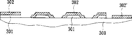
如图3A所示,其中一玻璃基板300作为绝缘的透明基板,其上沉积一由金属或合金形成的第一金属层(metal)301,可以沉积(depositing)方式实施,之后经蚀刻形成此TFT元件的栅极(gate electrode)与周边保护电路元件等,实际应用可运用如图标多极的TFT结构,并不限于此述的结构。As shown in FIG. 3A, one of the
图3B所示则于玻璃基板300与第一金属层301上形成一透明导电电极(ITO)302,可以溅镀(sputtering)的制程实施,并经蚀刻可成为此TFT元件的像素电极,有别于现有技术第一金属层制作于透明导电电极之后。此透明导电电极302的形成包覆第一金属层301,以阻绝与避免第一金属层301因于高温制程下的金属离子扩散现象,尤其针对以铜为主要材料的第一金属层301扩散现象,并且经蚀刻过程后,此透明导电电极302同时可作为此TFT元件的像素电极302’。As shown in FIG. 3B, a transparent conductive electrode (ITO) 302 is formed on the
再如图3C所示,于透明导电电极302上形成一介电层(dielectric)303作为隔绝层,可为氧化硅(silicon oxide)、氮化硅(silicon nitride)或是两者的组合所形成的多层结构,并以等离子体增益化学气相沉积(Plasma Enhance Chemical Vapor Deposition,PECVD)作为其一实施方式,此为一高温制程,第一金属层301以上述的透明导电电极302包覆,故可避免此高温制程造成金属离子扩散造成的漏电或不良导电现象。As shown in FIG. 3C, a dielectric layer (dielectric) 303 is formed on the transparent
接着,请参阅图3D所示的一非晶硅层(amorphous silicon,a-Si)304形成的半导体层,此非晶硅层304可为单层或多层结构,可以等离子体化学沉积法实施,之后于此非晶硅层304上以等离子体增益化学气相沉积法直接沉积N+非晶硅层或以离子注入方式(ion implanting)将N+离子注入于非晶硅层304上方,形成非晶硅层304a与N+非晶硅层304b两层。Next, please refer to the semiconductor layer formed by an amorphous silicon layer (a-Si) 304 shown in FIG. 3D. This amorphous silicon layer 304 can be a single-layer or multi-layer structure, and can be implemented by plasma chemical deposition. , and then directly deposit an N+ amorphous silicon layer on the amorphous silicon layer 304 by plasma-enhanced chemical vapor deposition or implant N+ ions above the amorphous silicon layer 304 by ion implanting to form
接续的制程如图3E所示,显示为第二金属层305形成于该N+非晶硅层304b上,将N+非晶硅层304b与第二金属层305依实际需求以蚀刻方式形成此薄膜晶体管元件的源极(source)与漏极(drain)两极(305’,305”),并其它元件层。在此所述的第二金属层(metal II)305亦可为多层金属层的结构,并不限于此。The subsequent manufacturing process is shown in FIG. 3E, which shows that the
再如图3F所示,由一钝化层(passivation film)306形成一此TFT元件的保护层,但此钝化层306并非必要,且仍可量测此TFT元件的极性。并依需要可形成该TFT元件侧边的保护电路308a,元件的三极结构308b与像素电极302’。As shown in FIG. 3F again, a passivation layer (passivation film) 306 is used to form a protection layer for the TFT element, but the
本发明以像素透明电极接续栅极金属层(Metal I)之后制作可一方面作为金属离子的阻障层,可避免金属离子高温扩散至介电层形成的隔绝层甚至主动层。另一方面PVD机台可于低温镀膜、对环境的敏感度较小,且本身为导电层,可避免金属离子的影响。本发明以新制程达成降低金属离子污染CVD制程的风险。In the present invention, the pixel transparent electrode is connected to the gate metal layer (Metal I) to form a barrier layer for metal ions on the one hand, which can prevent the high-temperature diffusion of metal ions to the insulating layer or even the active layer formed by the dielectric layer. On the other hand, PVD machines can coat films at low temperatures, are less sensitive to the environment, and are conductive layers themselves, which can avoid the influence of metal ions. The invention uses a new process to reduce the risk of metal ions contaminating the CVD process.
而图4所示为本发明防止金属层扩散的TFT电极制程步骤流程图,此实施例为一单极结构的TFT晶体管,熟悉此项技术者可轻易延伸应用于多极结构的薄膜晶体管制程。4 is a flow chart of the TFT electrode manufacturing process for preventing metal layer diffusion according to the present invention. This embodiment is a TFT transistor with a unipolar structure, and those skilled in the art can easily extend it to a thin film transistor manufacturing process with a multipolar structure.
步骤S41:于透明基材上以物理气相沉积(PVD)、电镀(EP)、旋镀(Spincoating)、印制(printing)或无电镀(ELP)方式等物理气相沉积法沉积第一金属层,并经蚀刻方法定义图形,并形成TFT元件的栅极。Step S41: Depositing the first metal layer on the transparent substrate by physical vapor deposition (PVD), electroplating (EP), spin coating (Spincoating), printing (printing) or electroless plating (ELP) methods, etc., And the pattern is defined by the etching method, and the gate of the TFT element is formed.
此外,该基材表面具有玻璃、氮化硅、氧化硅、非结晶硅、结晶硅、掺杂质的硅、金属层、金属氮化物、金属氮硅化物、聚合物、或有机材料。金属可为单层金属或多层结构,单一金属层可为铬、铜、铝钕合金(Al-Nd)、钼钨合金(MOW)、或铝。多层结构可为:钛/铝/钛层(Ti/Al/Ti)、钛/铝/氮化钛层(Ti/AI/TiN)、钛/铜/钛层(Ti/Cu/Ti)、铬/铜/铬层(Cr/Cu/Cr)、钨/铜/钨层(W/Cu/W)、氮化钼/铝/氮化钼层(MoN/Al/MoN)、钼/铝钕合金层(Mo/Al-Nd)、氮化钼/铝钕合金层(MoN/Al-Nd)、钼/铝钕合金/钼层(Mo/Al-Nd/Mo)、钽/铜/钽层(Ta/Cu/Ta)、氮化钽/铜/氮化钽层(TaN/Cu/TaN)、氮化钛/铜/氮化钛层(TiN/Cu/TiN)、钛/铝层(Ti/Al)、钼/铜/钼层(Mo/Cu/Mo)、或钼/铝/钼层(Mo/Al/Mo)。In addition, the surface of the substrate has glass, silicon nitride, silicon oxide, amorphous silicon, crystalline silicon, doped silicon, metal layer, metal nitride, metal nitride silicon nitride, polymer, or organic material. The metal can be a single-layer metal or a multi-layer structure, and the single metal layer can be chromium, copper, aluminum-neodymium alloy (Al-Nd), molybdenum-tungsten alloy (MOW), or aluminum. The multilayer structure can be: titanium/aluminum/titanium layer (Ti/Al/Ti), titanium/aluminum/titanium nitride layer (Ti/AI/TiN), titanium/copper/titanium layer (Ti/Cu/Ti), Chromium/Cu/Cr (Cr/Cu/Cr), W/Cu/W (W/Cu/W), MoN/Al/MoN (MoN/Al/MoN), Mo/AlNd Alloy layer (Mo/Al-Nd), molybdenum nitride/aluminum neodymium alloy layer (MoN/Al-Nd), molybdenum/aluminum neodymium alloy/molybdenum layer (Mo/Al-Nd/Mo), tantalum/copper/tantalum layer (Ta/Cu/Ta), tantalum nitride/copper/tantalum nitride layer (TaN/Cu/TaN), titanium nitride/copper/titanium nitride layer (TiN/Cu/TiN), titanium/aluminum layer (Ti /Al), molybdenum/copper/molybdenum layer (Mo/Cu/Mo), or molybdenum/aluminum/molybdenum layer (Mo/Al/Mo).
步骤S42:沉积形成透明导电电极如:ITO(indium tin oxide)、IZO(Indium zinc oxide)、ZnO(zinc oxidation)或有机材料等,沉积方式可为物理气相沉积法(PVD)、电镀(EP)、旋镀(spin coating)、印制(printing)或无电镀(ELP)方式,并经蚀刻定义图形,形成像素电极。Step S42: Deposit to form a transparent conductive electrode such as: ITO (indium tin oxide), IZO (Indium zinc oxide), ZnO (zinc oxidation) or organic materials, etc. The deposition method can be physical vapor deposition (PVD), electroplating (EP) , spin coating (spin coating), printing (printing) or electroless plating (ELP) method, and etched to define the pattern to form the pixel electrode.
以下可为通常的TFT制程:The following can be the usual TFT manufacturing process:
步骤S43:形成作为绝缘层的介电层,可为二氧化硅、氮化硅等。Step S43 : forming a dielectric layer as an insulating layer, which may be silicon dioxide, silicon nitride, or the like.
步骤S44:于介电层上形成一或多个非晶硅层的半导体层,以改善薄膜晶体管特性。Step S44 : forming one or more amorphous silicon semiconductor layers on the dielectric layer to improve the characteristics of the thin film transistor.
步骤S45:于该非晶硅层上以等离子体增益化学气相沉积法直接沉积N+非晶硅层或以离子注入方式将N+离子注入上,形成一离子浓度较高的N+非晶硅层。Step S45 : directly depositing an N+ amorphous silicon layer on the amorphous silicon layer by plasma-enhanced chemical vapor deposition or implanting N+ ions by ion implantation to form an N+ amorphous silicon layer with a higher ion concentration.
步骤S46:再于N+非晶硅层上形成第二金属层。Step S46: forming a second metal layer on the N+ amorphous silicon layer.
步骤S47:经蚀刻步骤形成此TFT元件的源极与漏极。Step S47: forming the source and drain of the TFT element through an etching step.
步骤S48:形成一钝化层作为此TFT元件的保护层。Step S48: forming a passivation layer as a protection layer for the TFT element.
综上所述,本发明提供一种防止金属层扩散的TFT电极结构与其制程,以防止于薄膜晶体管(TFT)的金属层制作时会扩散至邻近的绝缘层,以改善TFT制程的漏电现象与不良导电的情形。To sum up, the present invention provides a TFT electrode structure and its manufacturing process that prevent the diffusion of the metal layer, so as to prevent the metal layer of the thin film transistor (TFT) from being diffused to the adjacent insulating layer when the metal layer is fabricated, so as to improve the leakage and leakage of the TFT manufacturing process. A case of poor electrical conductivity.
Claims (21)
Priority Applications (1)
| Application Number | Priority Date | Filing Date | Title |
|---|---|---|---|
| CNB2004100626929A CN100405547C (en) | 2004-08-06 | 2004-08-06 | TFT electrode structure for preventing metal layer from diffusion and its manufacturing process |
Applications Claiming Priority (1)
| Application Number | Priority Date | Filing Date | Title |
|---|---|---|---|
| CNB2004100626929A CN100405547C (en) | 2004-08-06 | 2004-08-06 | TFT electrode structure for preventing metal layer from diffusion and its manufacturing process |
Publications (2)
| Publication Number | Publication Date |
|---|---|
| CN1731562A CN1731562A (en) | 2006-02-08 |
| CN100405547C true CN100405547C (en) | 2008-07-23 |
Family
ID=35963895
Family Applications (1)
| Application Number | Title | Priority Date | Filing Date |
|---|---|---|---|
| CNB2004100626929A Expired - Fee Related CN100405547C (en) | 2004-08-06 | 2004-08-06 | TFT electrode structure for preventing metal layer from diffusion and its manufacturing process |
Country Status (1)
| Country | Link |
|---|---|
| CN (1) | CN100405547C (en) |
Families Citing this family (6)
| Publication number | Priority date | Publication date | Assignee | Title |
|---|---|---|---|---|
| JP2009020199A (en) * | 2007-07-10 | 2009-01-29 | Mitsubishi Electric Corp | Display panel and manufacturing method thereof |
| JP5361651B2 (en) * | 2008-10-22 | 2013-12-04 | 株式会社半導体エネルギー研究所 | Method for manufacturing semiconductor device |
| CN103646966B (en) * | 2013-12-02 | 2016-08-31 | 京东方科技集团股份有限公司 | A kind of thin film transistor (TFT), array base palte and preparation method thereof, display device |
| CN106784013A (en) * | 2016-11-29 | 2017-05-31 | 京东方科技集团股份有限公司 | A kind of thin film transistor (TFT), array base palte and display device |
| CN107316907A (en) * | 2017-06-23 | 2017-11-03 | 南京中电熊猫液晶显示科技有限公司 | Coplanar type thin film transistor (TFT) and its manufacture method |
| JP7512672B2 (en) * | 2020-05-20 | 2024-07-09 | セイコーエプソン株式会社 | Piezoelectric element, liquid ejection head and liquid ejection device |
Citations (4)
| Publication number | Priority date | Publication date | Assignee | Title |
|---|---|---|---|---|
| US5838037A (en) * | 1996-11-15 | 1998-11-17 | Mitsubishi Denki Kabushiki Kaisha | TFT-array and manufacturing method therefor |
| US6218221B1 (en) * | 1999-05-27 | 2001-04-17 | Chi Mei Optoelectronics Corp. | Thin film transistor with a multi-metal structure and a method of manufacturing the same |
| US20010030717A1 (en) * | 2000-01-07 | 2001-10-18 | Hitachi, Ltd. | Liquid crystal display device |
| TW588462B (en) * | 2003-03-31 | 2004-05-21 | Quanta Display Inc | Method of fabricating a thin film transistor array panel |
-
2004
- 2004-08-06 CN CNB2004100626929A patent/CN100405547C/en not_active Expired - Fee Related
Patent Citations (4)
| Publication number | Priority date | Publication date | Assignee | Title |
|---|---|---|---|---|
| US5838037A (en) * | 1996-11-15 | 1998-11-17 | Mitsubishi Denki Kabushiki Kaisha | TFT-array and manufacturing method therefor |
| US6218221B1 (en) * | 1999-05-27 | 2001-04-17 | Chi Mei Optoelectronics Corp. | Thin film transistor with a multi-metal structure and a method of manufacturing the same |
| US20010030717A1 (en) * | 2000-01-07 | 2001-10-18 | Hitachi, Ltd. | Liquid crystal display device |
| TW588462B (en) * | 2003-03-31 | 2004-05-21 | Quanta Display Inc | Method of fabricating a thin film transistor array panel |
Also Published As
| Publication number | Publication date |
|---|---|
| CN1731562A (en) | 2006-02-08 |
Similar Documents
| Publication | Publication Date | Title |
|---|---|---|
| US8759832B2 (en) | Semiconductor device and electroluminescent device and method of making the same | |
| US6166396A (en) | Semiconductor devices | |
| US6887776B2 (en) | Methods to form metal lines using selective electrochemical deposition | |
| US8164097B2 (en) | Thin film transistor array panel and manufacturing method thereof | |
| US20160043227A1 (en) | Thin film transistor and manufacturing method thereof | |
| US20070278497A1 (en) | Thin film transistor substrate and display device | |
| US20140061635A1 (en) | Array Substrate, Manufacturing Method And The Display Device Thereof | |
| US9646997B2 (en) | Array substrate, method for manufacturing the same and display device | |
| US9337213B2 (en) | Semiconductor device and method for manufacturing same | |
| KR101004219B1 (en) | Wiring, wiring formation method, thin film transistor and display device | |
| CN104282576B (en) | A kind of metal oxide thin-film transistor preparation method | |
| CN103579115B (en) | Complementary thin-film transistor and preparation method thereof, array base palte, display unit | |
| US9704998B2 (en) | Thin film transistor and method of manufacturing the same, display substrate, and display apparatus | |
| US7045817B2 (en) | Structure of TFT electrode for preventing metal layer diffusion and manufacturing method therefor | |
| US20120161131A1 (en) | Thin-film transistor substrate and method of manufacturing the same | |
| CN103531640A (en) | Thin film transistor, array substrate, manufacturing method of array substrate and display device | |
| CN103489902B (en) | A kind of electrode and preparation method thereof, array base palte and display unit | |
| US20190131322A1 (en) | Method for manufacturing thin-film transistor and thin-film transistor | |
| CN100405547C (en) | TFT electrode structure for preventing metal layer from diffusion and its manufacturing process | |
| CN103489900B (en) | A kind of barrier layer and preparation method thereof, thin film transistor (TFT), array base palte | |
| CN104409516A (en) | Thin film transistor and manufacturing method thereof, array substrate and manufacturing method thereof and display device | |
| US20190371827A1 (en) | Flexible thin film transistor and manufacturing method therefor | |
| CN110504164B (en) | Thin film transistor, method of manufacturing the same, and display device | |
| KR20060001753A (en) | Organic electroluminescent device and manufacturing method thereof | |
| CN101409308A (en) | Thin film transistor, pixel structure and manufacturing method thereof |
Legal Events
| Date | Code | Title | Description |
|---|---|---|---|
| C06 | Publication | ||
| PB01 | Publication | ||
| C10 | Entry into substantive examination | ||
| SE01 | Entry into force of request for substantive examination | ||
| C14 | Grant of patent or utility model | ||
| GR01 | Patent grant | ||
| CF01 | Termination of patent right due to non-payment of annual fee | ||
| CF01 | Termination of patent right due to non-payment of annual fee |
Granted publication date: 20080723 Termination date: 20190806 |