Cryogenics 47 (2007) 243–251
www.elsevier.com/locate/cryogenics
Silicon power MOSFET at low temperatures:
A two-dimensional computer simulation study
Hua Ye
a,*
, Changwoo Lee a, James Raynolds a, Pradeep Haldar a, Michael J. Hennessy b,
Eduard K. Mueller b
a
College of Nanoscale Science and Engineering, State University of New York at Albany, Albany, NY 12203, USA
b
MTECH Laboratories, LLC, Ballston Spa, NY 12020, USA
Received 6 July 2006; received in revised form 25 January 2007; accepted 30 January 2007
Abstract
Understanding how the structure of the unit-cell affects the cryogenic performance of a Si power Metal Oxide Semiconductor Field
Effect Transistor (MOSFET) is an important step toward optimizing of the device for cryogenic operations. In this paper, numerical
simulations of the Si power Double Diffused MOSFET’ (DMOS) are performed at room temperature and cryogenic temperatures.
Physically based models for temperature dependent silicon properties are employed in the simulations. The performances of power
DMOS’ with various unit-cell structures are compared at both room temperature and low temperatures. The effect of the cell structure
on the on-resistance and breakdown voltage of the device are analyzed. The simulation results suggest that the device optimized for room
temperature operation can be further optimized at cryogenic temperatures.
� 2007 Elsevier Ltd. All rights reserved.
Keywords: Cryogenic power electronics; Power MOSFET; Numerical simulation
1. Introduction
Extensive research has been focused on development of
cryogenic power electronics system recently [1–11]. The
interest of investigating cryogenic power electronics comes
from the idea of building power conditioning systems with
much higher efficiency by cooling power devices down to
cryogenic temperatures and by combining them with High
Temperature Superconductor (HTS) components in order
to gain synergistic benefits [12]. The development of superconducting hybrid power electronics system is becoming an
enabler in future military system where substantial electric
power will be needed to operate combatant ships, electric
air aircraft, and directed energy weapons [13]. Cryogenic
power electronics is of interest to deep space exploration
where low temperature is the norm than the exception.
*
Corresponding author. Tel.: +1 518 591 8016; fax: +1 518 591 8011.
E-mail address: hye@uamail.albany.edu (H. Ye).
0011-2275/$ - see front matter � 2007 Elsevier Ltd. All rights reserved.
doi:10.1016/j.cryogenics.2007.01.007
Due to the better electronic, electrical, and thermal properties of certain semiconductor materials at low temperatures
[14–16], cryogenic power electronics is expected to have
better efficiency, higher speed, reduced leakage current,
and reduced latch-up susceptibility [15–17]. For instance,
as a majority carrier device, the performance of Si power
MOSFET at low temperatures improves due to increased
carrier mobility, higher transconductance, steeper subthreshold slope, and reduced junction leakage [18–20].
However, as Jackson et al. argued, it was not likely that
existing devices were truly optimized for cryogenic environment and developments of optimized cryogenic devices
were required [2].
Numerical simulation study of the Si power MOSFET’s
at cryogenic temperatures can be used as an important step
toward optimizing power electronics for cryogenic operations. Very few numerical simulations of Si power MOSFET under cryogenic temperatures have been reported in
the published literature [21,22]. In this paper, we compare
�244
H. Ye et al. / Cryogenics 47 (2007) 243–251
the performances of power DMOS’ with various unit-cell
structures at both room temperature and low temperatures
using two-dimensional numerical simulations. The dependence of the cell structure on the threshold voltage, the
breakdown voltage, and the on-resistance of the device
are analyzed. The simulation results suggest that the device
optimized for room temperature operation can be further
optimized at cryogenic temperatures.
unit-cell, which gave the characteristic current values for
a circular unit-cell. In order to give the current density
(A/cm2), the unit-cell current values will be multiplied by
the number of unit-cells that can be accommodated in
1 cm2 area (e.g., for the circular baseline unit-cell with a
diameter of 30 lm, a multiplier of 1.11 · 105 will be used).
When a positive voltage is applied at the gate electrode,
a conductive path (inversion channel) is created across the
p-base region underneath the gate. The total on-resistance
(Ron) of a power DMOS is determined by all the resistive
components as given by [23]:
2. Device simulation description
Ron ¼ RSource þ RCH þ RA þ RJFET þ RD þ RSub
Power DMOS’ are vertical conduction devices which
comprise a repetitive array of unit-cells arranged in a topological layout (such as linear, square array, circular array,
atomic lattice layout, and hexagonal array). Therefore, it
is necessary to simulate the performance of the elementary
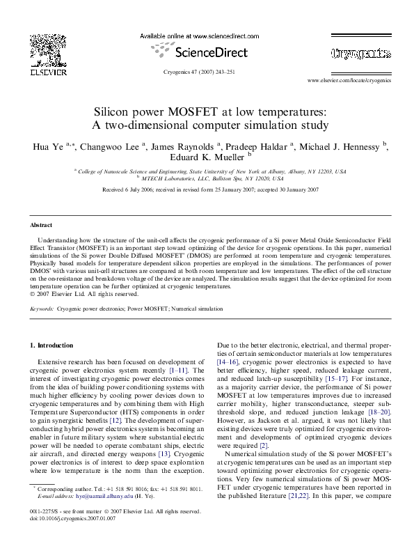
unit-cell. Fig. 1a and b show the baseline unit-cell of a
medium-voltage DMOS and the half unit-cell used in the
numerical simulation due to symmetry, respectively. This
information was obtained from first-order analytical calculations. In the baseline unit-cell, the p-base depth was 4 lm
and n+ source depth was 1 lm, yielding a channel length of
2.4 lm (with lateral diffusion as 80% of the vertical depth).
Gaussian profiles have been assumed for n+ source and
p-base with the peak concentrations of 3 · 1017 and
1 · 1019 cm�3, respectively. The starting epi-layer thickness
was 52 lm and the doping concentration was 3 · 1014
cm�3. The n+ substrate had a concentration of 1 ·
1019 cm�3 with the actual thickness of n+ substrate was
300 lm. However, in the simulation, a thickness of 20 lm
was used in order to save the computational time. Due to
very high doping concentration in the n+ substrate, which
behaves like a conductor, this approximation had minimum effect on the simulation results. The gate oxide thickness was assumed to be 100 nm with a gate-length of 12 lm
in the baseline unit-cell. In this study, the topological
design was assumed to be circular cell in square array.
Cylindrical symmetry was assumed in simulating the half
where RSource is the n+ source resistance, RCH is the
channel resistance, RA is the accumulation layer resistance,
RJFET is the contribution from the drift region between the
p-base regions, RD is the drift region resistance, and RSub
is the substrate resistance. However, due to the high doping concentrations in the source and substrate regions,
RSource and RSub are negligible for high voltage power
devices [24].
In this simulation work, the physically-based two and
three-dimensional device simulation software ATLAS [25]
has been used. The operation of the semiconductor device
is modeled by a set of Partial Differential Equations
(PDEs) with appropriate models for various temperature
dependent semiconductor properties. ATLAS uses Box
Integration Method to solve these simultaneous PDEs
numerically on a discrete grid of points which is referred
to as mesh points. All the simulations in this study have
been performed in two dimensions. A variable mesh spacing has been used by refining the mesh in the critical
regions (such as in the channel and junctions regions) in
order to increase the accuracy without overly lengthening
the computational time. Cylindrical symmetry was also
employed for this purpose.
The drift-diffusion models for the steady-state are based
on the three PDEs:
30
15
N+ substrate 1e19
Drain
1
4
N- drift 3e14
1.7
48
5.6
Source
20
N+ source 1e19
2.4
8.1
P base 3e17
1
n-PolySi
N+ source 1e19
8.1
2.4
P base 3e17
Source
4
1.7
Gate Oxide 100nm
48
Source
20
Gate
1.7
Gate
N+ source 1e19
8.1
2.4
P base 3e17
n-PolySi
2.8
N- drift 3e14
N+ substrate 1e19
Drain
Fig. 1. (a) Cross-sectional view of the DMOS unit-cell showing the dimensions and impurity concentrations and (b) half unit-cell used in the simulation.
�H. Ye et al. / Cryogenics 47 (2007) 243–251
�
~ � ðerWÞ
~
Poisson’s equation : r
¼ qðn � p � N þ
D þ N A Þ ð1Þ
~ � ð~
ð2Þ
electron continuity equation : r
J n Þ ¼ qR
~ � ð~
hole continuity equation : r
J p Þ ¼ �qR
ð3Þ
~ � ln nrWÞ
~
and ~
J n ¼ qðDn rn
~ � lp prWÞ
~
~
J p ¼ qð�Dp rp
ð4Þ
ð5Þ
where W is the electrical potential, n and p are the concentrations of electrons and holes, respectively, Dn, Dp, ln, lp
are diffusivity and mobility of electrons and holes, respectively, e is the electric permittivity of the material, q is
electron charge, R is the net electron–hole recombination
rate, Jn and ~
J p are electron and hole current density,
�
respectively, N þ
D and N A are the concentration of the ionized donor and ionized acceptor.
In order to model the device characteristics at low temperatures, incomplete ionization and Fermi–Dirac statistics
are employed in the simulations. At room temperature,
impurities are usually assumed to be fully ionized. However, impurity freeze-out effects kick in at low temperatures. Moderately doped semiconductors are modeled
using Fermi–Dirac statistics with appropriate degeneracy
factors for conduction and valance bands [26]. For degenerately (>3 · 1018 cm�3) doped semiconductors, complete
ionization is assumed [25]. The use of Boltzman statistics
is normally justified in semiconductor device theory and
simple to be implement in the analysis; however, in order
to more accurately simulate the low temperature performance of semiconductors, Fermi–Dirac statistics is used
in this study. The effective density of states in silicon are
considered temperature dependent [25]. In the simulations,
the temperature dependence of the bandgap energy for silicon is considered and taken from Sze [27]. Bandgap narrowing was not considered in this study since it has little
effect on the performance of power DMOS at low
temperatures.
The temperature dependence of carrier mobility is the
most important factor that affects the performance of
power DMOS’ at low temperatures. At lower temperatures, the vibration of the lattice is reduced resulting in less
frequent scattering from the lattice. Therefore, carrier
mobility increases as temperature decreases. In order to
accurately model carrier mobility, various scattering mechanisms need to be considered. For low field bulk mobility,
Klaassen’s [28,29] unified mobility model is used in this
study. Klaassen’s model considers the effects of lattice scattering, impurity scattering, carrier–carrier scattering, and
impurity clustering effects at high concentration. The
model agrees well with the empirical data for a wide range
of donor and acceptor concentrations with temperature
dependence over the range of 70–500 K. For the mobility
degradation within the inversion layers, Lombardi et al.’s
[30] model is used to include the effects of surface acoustic
phonon scattering and surface roughness scattering. In our
simulation, the Klaassen model is used to calculate bulk
mobility instead of Lombardi et al.’s original model. For
245
high field velocity saturation, Caughey and Thomas’s
model [31] is used to calculate the carrier mobility. The saturation velocities are considered as temperature-dependent
[32], where the saturation velocity of silicon increases about
20% when cooled from 300 K to 77 K.
Shockley–Read–Hall (SRH) and Auger recombination
were considered in this simulation work. SRH recombination accounts for phonon transitions in the presence of a
trap (or defect) within the bandgap of the semiconductor.
The SRH carrier lifetime is considered to be concentration
and temperature-dependent as proposed by Klaassen [28].
Auger recombination describes a three-particle transition
whereby a mobile carrier is either captured or emitted
[33]. When the reverse bias is sufficiently large, the electric
field in the space charge region will be high enough to
accelerate free carriers up to sufficiently high kinetic energy
to cause avalanche breakdown. At lower temperatures the
mean free path of carriers increases, giving them more
energy for a given electric field prior to collisions, thus
resulting in a reduced avalanche breakdown voltage. The
phenomenological local electric field model proposed by
Selberherr [33] was employed in this study. Numerical simulation of breakdown at low temperatures can be difficult
because the depletion regions have too few carriers to start
an avalanche due to the extremely low intrinsic carrier concentration at 77 K. In order to overcome this numerical difficulty, a small beam of light was artificially shined on the
top surface of the DMOS to provide carriers which can
start the avalanche when conditions are right [25]. This
technique is routinely practiced even at room temperature
where extremely low intrinsic carrier concentration causes
numerical convergence problems such as simulation studies
in certain SiC based devices. The wavelength of this artificial light was 800 nm and the beam intensity was
0.001 Watt/cm2 in the simulations. We checked the effects
of different beam intensities on simulation results in order
to make sure that this artificial light did not affect the accuracy of the breakdown voltage.
3. Simulation results and discussions
3.1. Baseline unit-cell
Steady-state I–C characteristics, threshold characteristics, and breakdown characteristics of baseline power
DMOS unit-cell have been simulated as shown in Fig. 2.
It is shown in Fig. 2a and b that the on-resistance of the
power DMOS unit-cell decreases with temperature. This
is due to the higher electron mobility at lower temperatures. In Fig. 2b, the specific current (A/cm2) is calculated
by multiplying the drain current of the unit-cell by the
number of unit-cells that can be accommodated in a
1 cm2 area. The specific on-resistance (X cm2) is calculated
by dividing the drain–source voltage with the corresponding specific current. Fig. 2c shows that, at 77 K, the DMOS
has higher threshold voltage (from 4.75 V at 300 K to 6.0 V
at 77 K), transconductance, and current saturation level.
�246
H. Ye et al. / Cryogenics 47 (2007) 243–251
2.5
0.00014
Specific on-resistance (Ω cm2)
Drain Current (A)
Vgate = 10 V
300K
77K
0.00012
Baseline unit-cell
0.00010
0.00008
0.00006
0.00004
0.00002
300K
77K
2.0
1.5
1.0
Vgate = 10 V
0.5
Baseline unit-cell
0.00000
0.0
0
2
4
6
8
10
12
14
0
5
4e-5
15
20
1.4e-8
Drain Current (A)
Vds = 1 V
2e-5
300K
77K
1.2e-8
300K
77K
3e-5
Drain Current (A)
10
Specific current (A/cm2)
Drain-Source Voltage (V)
Baseline unit-cell
1e-5
1.0e-8
Vgate = 0 V
8.0e-9
baseline unit cell
6.0e-9
4.0e-9
2.0e-9
0.0
0
0
1
2
3
4
5
6
7
8
9
10
Gate-Source Voltage (V)
0
100
200
300
400
500
600
700
Drain-Source Voltage (V)
Fig. 2. Characteristics of baseline DMOS unit-cell at 300 K and 77 K: (a) I–V characteristics at Vgate = 10 V, (b) specific on-resistance vs. current, (c)
threshold characteristics at Vds = 1 V and (d) breakdown characteristics.
The intrinsic carrier concentration decreases 30 orders of
magnitude at 77 K resulting in increased band-bending in
the p-base region, which needs to be compensated by a
higher gate voltage in order to inverse the channel [34].
The higher transconductance at 77 K is due to the
increased channel mobility whereas the higher current saturation level is due to the higher electron mobility in all the
device regions. Fig. 2d shows that the blocking voltage of
the baseline unit-cell decreases significantly from 660 V at
300 K to 510 V at 77 K, a 23% reduction. At lower temperatures, the mean free path of the carrier increases giving
free carrier more energy for a given electric field prior to
collision, thus resulting in a reduced avalanche breakdown
voltage.
Although the on-resistance of the baseline unit-cell
shows moderate improvement at 77 K, it is far less than
the improvement we expected. As shown in Fig. 2a, the
drain–source current of the baseline unit-cell increased by
a factor of 5.6 at 77 K compared to that at 300 K at a very
low specific current level and much less at higher current
level. Let’s now look into the electrical field within the
unit-cell.
Fig. 3 shows the potential and electrical field of the baseline unit-cell at Vds = 3 V with a gate voltage of 10 V at
300 K. The electrical field along the p-base and n-epi junction expands into the region between the p-bases which is
sometimes referred to as the JFET region (Fig. 3b). Along
the current flow path, most of the applied drain–source
voltage is taken by the JFET region (Fig. 3b), which contributes to the most of the series resistance of the baseline
unit-cell.
As previously mentioned, the on-resistance improvement of power DMOS at lower temperature is a direct
result of the increased carrier mobility. Fig. 4a compares
the electron mobility distribution within the baseline half
unit-cell at 300 K and 77 K under a drain–source voltage
of 3 V. Due to the impurity scattering, the electron mobility
in the high doping region does not increase much at 77 K.
The electron mobility in the accumulation and the channel
regions has moderate increase at 77 K due to surface scattering. While electron mobility increases by a factor of over
10 in the lightly doped epi-layer at 77 K compared to that
at 300 K, it only increases by a small amount in the JFET
region for the baseline unit-cell. Fig. 4c shows that, in the
JFET region, while the horizontal electrical fields are
low, the vertical electrical fields (parallel to the current
flow) are high at both temperatures. This high parallel electrical field in the JFET region corresponds to the limited
improvement of electron mobility at 77 K in this region
as shown in Fig. 4b. We believe the reason for the limited
electron mobility improvement in JFET region is due to
electron velocity saturation. Fig. 4d shows the electron
velocities in the JFET region with various drain–source
voltages at 77 K. It is clearly shown that the peak electron
velocities in the JFET region saturate at about
1.3 · 107 cm/s. Therefore, in order to achieve the highest
�247
H. Ye et al. / Cryogenics 47 (2007) 243–251
Fig. 3. (a) Electrical field and (b) electrostatic potential of the baseline unit-cell with Vds = 3 V and Vgate = 10 V at 300 K.
18000
Electron mobility (cm2/Vs)
16000
14000
12000
10000
77K
300K
8000
6000
4000
2000
0
0
5
10
15
20
Y (micron)
1.4e+7
57500
77K - E Field X
77K - E Field Y
300K - E Field X
300K - E Field Y
55000
1.2e+7
Electron velocity (cm/s)
Electrical field (V/cm)
52500
Vds= 3V
Vds= 10V
Vds=30V
50000
5000
2500
0
-2500
1.0e+7
8.0e+6
6.0e+6
4.0e+6
T=77K
2.0e+6
-5000
0.0
-7500
0
5
10
15
20
Y (micron)
0
5
10
15
20
Y (micron)
Fig. 4. (a) Electron mobility distribution of the baseline unit-cell with Vg = 10 V and Vds = 3 V at 300 K and 77 K. (b) Electron mobility along the vertical
line through the center of the baseline unit-cell with Vg = 10 V and Vds = 3 V at 300 K and 77 K. (c) Electrical field along the vertical line through the
center of the baseline unit-cell with Vg = 10 V and Vds = 3 V at 300 K and 77 K. (d) Electron velocity along the vertical line through the center of the
baseline unit-cell with Vg = 10 V, Vds = 3 V, 10 V, and 30 V at 77 K.
cryogenic improvement, the structure of the baseline unitcell needs to be modified in such a way that the electrical
field in the JFET region can be reduced. Fortunately, the
electrical field in the JFET region in a unit-cell optimized
for room temperature operation is normally much smaller
than that in the baseline cell.
�248
H. Ye et al. / Cryogenics 47 (2007) 243–251
to the majority of the on-resistance of the unit-cell, the
on-resistance of the DMOS decreases by a factor of 10 at
77 K.
Fig. 6 shows the plot of the specific on-resistance vs. the
gate-length, where the value of specific on-resistance for a
particular gate-length is taken as the value at Vds = 0.5 V.
At 300 K, the optimized value of the gate-length is found
to be 80 lm while the optimized value of the gate-length
is 72 lm at 77 K. However, the difference is less than
0.5% between the 80 lm and 72 lm gate-length cells at
77 K. This means gate-length optimized for 300 K is effectively optimized for 77 K operation. The gate-length optimization of DMOS at cryogenic temperatures has been
analyzed before by Singh using an analytical approach
[34]. He concluded that the power DMOS with optimized
gate-length design for room temperature operation would
have more than 15% higher on-resistance than that optimized for 77 K operation. We believe the possible discrepancy might come from his calculation of JFET region
resistance, where mobility in the region was assumed to follow the same temperature dependence as that in the epilayer. It has been shown in our simulations that it does
not always hold true for smaller gate-lengths where parallel
electrical field is high.
3.2. Gate-length optimization
The effect of the gate-length on the cryogenic improvement of unit-cell was studied by conducting numerical simulations of unit-cells with various gate-lengths while other
design parameters remained constant. It is well known that
a larger gate-length leads to smaller JFET region resistance
but larger accumulation and channel resistance because of
the longer path along the oxide-Si surface as well as smaller
equivalent channel density [23]. Optimization is the best
approach to find the best trade-off between these major
on-resistance components. As the gate-length increases,
the electrical field in the JFET region decreases; therefore,
we can also expect on-resistance improvement at cryogenic
temperatures.
Fig. 5a shows, that as the gate-length increases to 72 lm,
not only the DMOS on-resistance decreases substantially
(compared to Fig. 2b from 12 lm) at room temperature,
but also the much higher (10·) cryogenic improvement is
achieved. Fig. 5b and c show the electrical field and
electron mobility along the center vertical line of the
72 lm-gate-length unit-cell at 300 K and 77 K. Compared with the baseline unit-cell, under a drain–source voltage of 3 V, the vertical electrical field is reduced by a
factor of 10. Without the existence of the high parallel electrical field in the JFET region, the electron mobility in the
region increases more than 10 times when cooled to 77 K
without suffering from the velocity saturation effect. Since
the drift region and the JFET region resistance contribute
3.3. Comparison with experimental results
Experimental characterizations were performed on commercially available power MOSFETs and compared to the
55000
0.20
77K-E Field X
77K-E Field Y
300K-E Field X
300K-E Field Y
54500
0.16
0.14
Electrical field (V/cm)
Specific On-resistance (Ω cm2)
0.18
77K
300K
0.12
0.10
0.08
0.06
54000
1000
500
0
0.04
-500
0.02
0.00
0
50
100
150
200
-1000
250
0
5
Specific current (A/cm2)
10
15
20
Y (micron)
Electron mobility (cm2/V s)
16000
14000
12000
77K
300K
10000
8000
6000
4000
2000
0
0
5
10
15
20
Y (micron)
Fig. 5. (a) Specific on-resistance vs. specific current, (b) electrical field along the central vertical line and (c) electron mobility along the central vertical line
of the 72 lm-gate-length unit-cell with Vg = 10 V and Vds = 3 V at 300 K and 77 K.
�H. Ye et al. / Cryogenics 47 (2007) 243–251
3.4. Epi-layer thickness optimization for cryogenic operation
2
Specific on-resistance (Ω cm )
0.30
300 K
77 K
0.25
0.20
0.15
0.10
0.05
0.00
10
20
30
40
50
60
70
80
90
100
110
120
Gate length (µm)
Fig. 6. Optimization of gate-length for the DMOS unit-cell.
simulation results. The tested device is a 1000 V vendor
rated power MOSFET with a measured breakdown voltage
of 1100 V. The tested device has a die area of 1.9 cm2. In
Fig. 7, both the measured current and on-resistance have
been normalized to 1 cm2 for comparison with simulation
results. The power MOSFETs were mounted on the Direct
Bonded Copper (DBC) and wire bonded for electrical connections. A Tektronix 371A curve tracer was used to measure the I–V characteristics of the integrated module at
both room temperature and liquid nitrogen temperature.
Since the curve tracer provides pulsed current with a pulse
width of 250 ls and repetition rate of 15 Hz, little temperature rise in the MOSFET was observed due to minimum
heat dissipation during testing. The power DMOS cell
structure used in the simulation has an epi-layer doping
concentration of 1.25 · 1014 cm�3, epi-layer thickness of
84 lm, and gate-length of 70 lm and the simulation found
its breakdown voltage to be 1120 V. As shown in Fig. 7, the
simulation results matched with experimental measurement
very well at both room temperature and 77 K even though
the exact cell structure of the tested devices is not known.
The simulation correctly predicted more than 14· reduction of the on-resistance for this particular device. At
77 K, the breakdown voltage of the tested devices was measured to be 860 V, which is also very close to the breakdown voltage of the simulated cell, 884 V.
0.7
Specific On-resistance (Ω cm2)
249
0.6
Measurement @ 300K
Simulation @ 300K
Measurement @ 77K
Simulation @ 77k
0.5
0.4
0.3
0.2
0.1
0.0
0
20
40
60
80
100
120
140
Drain Current(A/cm2)
Fig. 7. Comparison of Ron vs. drain current between measurements and
simulation results.
One of the purposes of this paper is to answer the question: ‘‘Does the commercially available power MOSFETs
also give optimized on-resistance although its breakdown
voltage is degraded?’’ Our analysis in the gate-length optimization showed that no additional optimization of gatelength is needed for cryogenic operation. However, we
found that epi-layer thickness could be reoptimized to gain
the most performance improvement at 77 K.
As mentioned earlier, the resistance from the epi-layer
contributed to the majority of the on-resistance for
medium to high voltage power MOSFETs. Higher voltage blocking capability requires thicker epi-layer and
lower doping concentration. Both factors increase device
on-resistance. Device design therefore requires optimization of a combination of the epi-layer thickness and the
doping concentration so that lowest specific on-resistance
can be achieved. For certain epi-layer doping levels, there
is a corresponding threshold thickness, above which a maximum blocking voltage will be reached no matter how thick
the epi-layer is; on the other hand, if the thickness is smaller than the threshold value, the blocking voltage will
decrease. The cell with this threshold thickness will have
the lowest on-resistance with the highest reachable blocking voltage for a specific epi-layer doping level. The
commercially available devices have an optimized combination of epi-layer doping level and thickness for room
temperature operation. However, we found that the optimized design for room temperature operation is not
optimal at 77 K. In our analysis, we conducted simulations
for cells with epi-layer doping concentrations from
1.25 · 1014 cm�3 to 3.5 · 1014 cm�3. This covers power
MOSFETs with breakdown voltages between 500 V and
1200 V at room temperature. The epi-layer thickness under
consideration ranged from 32 lm to 112 lm.
The simulation results of blocking voltage dependence
on epi-layer thickness for various epi-layer doping concentrations at both 300 K and 77 K are shown in Fig. 8. They
clearly demonstrate that there exists a threshold epi-layer
thickness for any specific doping level at certain temperature. Increasing the thickness above this threshold value
will increase the specific on-resistance without increasing
the blocking voltage. It also clearly shows that the threshold epi-thickness for certain doping levels at 77 K is significantly smaller than that at 300 K. It indicates that
commercially available devices, which are optimized for
room temperature operation, are not optimal for cryogenic
operation. The epi-layer thickness of device optimized for
room temperature operation can be reduced significantly
without reducing its blocking voltage at 77 K. This is
because, at 77 K, the mean free path of carriers increases
giving free carrier more energy for a given electric field
prior to collision, which effectively reduces the critical electrical field for avalanche breakdown. As the critical field
decreases, the threshold epi-layer thickness required to
reach critical field before punch-through also decreases
�250
H. Ye et al. / Cryogenics 47 (2007) 243–251
1.25e14
1.5e14
2e14
2.5e14
3e14
3.5e14
1000
800
1200
Block voltage (V)
Blocking Voltage (V)
1200
Optimized thickness
for 300K
600
1.25e14
1.5e14
2e14
2.5e14
3e14
3.5e14
1000
800
Optimized thickness for 77K
600
400
400
40
60
80
100
40
60
80
100
Epi-layer thickness (µm)
Epi-layer thickness (µm)
Fig. 8. Blocking voltage vs. epi-layer thickness: (a) 300 K and (b) 77 K.
Table 1
Summary of epi-layer thickness optimization at 300 K and 77 K
Doping
(cm�3)
1.25e14
1.50e14
2.00e14
2.50e14
3.00e14
3.50e14
Optimization for 300 K
Optimal
thickness (lm)
108
92
72
60
52
44
Optimization for 77 K
Blocking voltage (V)
Ron (X cm2)
300 K
77 K
Reduction
(%)
300 K
77 K
Improvement
(·)
1190
1025
814
682
591
524
901
778
619
519
451
401
24
24
24
24
24
23
0.5565
0.4058
0.2514
0.1767
0.1344
0.1042
0.0415
0.0322
0.0224
0.0175
0.0145
0.0122
13.4
12.6
11.2
10.1
9.3
8.5
due to the triangular shape of the electrical field near the pbase and epi-layer junction. The summary of epi-layer
thickness optimization for various doping levels at both
300 K and 77 K are listed in Table 1. It indicates while
more than 8–13 times on-resistance improvement (depending on the voltage rating) can be expected by cooling the
commercially available power MOSFETs to 77 K, the
device optimized for 77 K by reducing the epi-layer thickness can provide additional 5–10% on-resistance reduction
depending on its voltage rating.
4. Conclusion
Two-dimensional numerical simulation study of the Si
power DMOS’ at cryogenic temperatures is presented in
this paper. In the simulation, Fermi–Dirac statistics and
incomplete ionization are considered. Physical based models for temperature dependent silicon properties are
employed. The simulation results are compared with experimental measurements with good agreement. It is suggested
that any medium to high voltage power MOSFETs will get
huge on-resistance improvement (8–13 times, depending on
voltage rating) by cooling down to 77 K. The simulation
results also suggest that the gate-length of a power DMOS
cell optimized for room temperature operation is sufficiently optimized for cryogenic operations. However, the
epi-layer thickness optimal for room temperature operation can be reduced without significantly reducing its
Optimal
thickness (lm)
Blocking
voltage (V)
Ron @ 77 K
(X cm2)
Additional
reduction (%)
96
80
64
52
44
40
901
778
619
519
451
401
0.0377
0.0290
0.0207
0.0159
0.0131
0.0116
9.1
10.0
7.8
9.0
9.4
5.0
breakdown voltage at 77 K. This leads to another 10% in
on-resistance reduction.
References
[1] Gardiner AI, Johnson SA, Schempp E. Operation of power electronic
converters at cryogenic temperatures for utility energy conditioning
applications. In: Proceedings of the 31st energy conversion engineering conference, IECEC 96, vol. 4; 1996. p. 2209–14.
[2] Jackson WD, Mazzoni OS, Schempp E. Characteristics of semiconductor devices at cryogenic temperatures. In: Proceedings of the
intersociety energy conversion engineering conference, vol. 31; 1996.
p. 676–81.
[3] Giesselmann M, Mahund Z, Carson S. Investigation of power
MOSFET switching at cryogenic temperatures. In: 22nd international
power modulator symposium; 1996. p. 47–50.
[4] Lu W, Mauriello RJ, Sundaram KB, Chow LC. Switching characteristics of a power MOSFET with varying temperature. In: Southeastcon ’98 proceedings IEEE; 1998. p. 268–70.
[5] Schlogl AE, Deboy G, Lorenzen HW, Linnert U, Schulze HJ, Stengl
JP. Properties of CoolMOS between 420 K and 80 K – the ideal
device for cryogenic applications. In: ISPSD ’99, proceedings of the
11th international symposium on power semiconductor devices and
ICs, Toronto, Ont., Canada, May 26–28, 1999. p. 91–4.
[6] Patterson RL, Hammoud A, Dickman JE, Gerber S, Elbuluk M,
Overton E. Electronics for deep space cryogenic applications. In:
Proceedings of the 5th European workshop on low temperature
electronics; 2002. p. 207–10.
[7] Elbuluk ME, Hammoud A, Gerber SS, Patterson R. Cryogenic
evaluation of an advanced DC/DC converter module for deep space
applications. In: 37th IAS annual meeting on industry applications
conference, vol. 1; 2002. p. 227–33.
�H. Ye et al. / Cryogenics 47 (2007) 243–251
[8] Elbuluk ME, Gerber S, Hammoud A, Patterson RL. Performance of
power converters at cryogenic temperatures, In: 37th IAS annual
meeting industry applications conference, vol. 1; 2001. p. 153–6.
[9] Elbuluk ME, Hammoud A, Gerber S, Patterson R, Overton E.
Performance of high-speed PWM control chips at cryogenic temperatures. IEEE Trans Ind Appl 2003;39(2):443–50.
[10] Hammoud A, Patterson RL, Gerber S, Elbuluk M. Electronic
components and circuits for extreme temperature environments. In:
Proceedings of the 2003, 10th IEEE international conference on
electronics, circuits and systems, vol. 1; 2003. p. 44–7.
[11] Hennessy MJ. Electronics for power systems at low temperatures. In:
Workshop on extreme environments technologies for space exploration, Pasadena, CA; 2003.
[12] Haldar P, Ye H, Efstathiadis H, et al. Improving performance of
cryogenic power electronics. IEEE Trans Appl Superconduct 2005;
15:2370–5.
[13] Curcic T, Wolf SA. Superconducting hybrid power electronics for
military systems. IEEE Trans Appl Superconduct 2005;15:2364–9.
[14] Kirschman RK. Low-temperature electronics. Circuits Dev Magazine, IEEE 1990;6:12–24.
[15] Dean M, Foty D, Saks N, Raider S, Oleszel G. Low temperature
microelectronics: opportunities and challegnes. In: Proceedings of the
symposium low temperature electronic device operation, electrochemical society, vol. 91; 1991. p. 25–37.
[16] Ray B, Gerber SS, Patterson RL, Myers IT. Power control electronics
for cryogenic instrumentation. Advances in Inst and Control, 50, 1,
Int Soc for Measurement and Control. 1995;131–9.
[17] Kirschman RK. Cold electronics: an overview. Cryogenics 1985;25:
115–22.
[18] Pierret RF. Modular series on solid state devices. Semiconductor
fundamentals, 2nd ed., vol. I. Reading Massachusetts: AddisonWesley Pub Co.; 1989.
[19] Baker RJ, Li HW, Boyce DE. COMS circuit design layout and
simulation. Wiley-IEEE Press; 1998.
[20] Ghazavi P, Fat DH. A numerical model for MOSFET’s from liquidnitrogen temperature to room temperature. IEEE Trans Electron Dev
1995;42:123–34.
251
[21] Vogler T, Schlogl A, Schroder D. Modeling and characterizing power
semiconductors at low temperatures. In: Proceedings of the 6th
international symposium on power semiconductor devices and ICs,
ISPSD ’94, Davos Switzerland; 1994. p. 237–42.
[22] Mauriello RJ, Sundaram KB, Chow LC. Simulation of Si power
MOSFET under cryogenic conditions. Solid State Electron 1999;43:
771–7.
[23] Baliga BJ. Power semiconductor devices. Boston: PWS Publishing
Company; 1996.
[24] Sun SC, Plummer JD. Modeling of the on-resistance of LDMOS,
VDMOS, and VMOS power transistors. IEEE Trans Electron Dev
1980;27:356–67.
[25] ATLAS Device Simulation Software [Version 5.8.3.R] Santa Clara,
CA, USA: SILVACO International; 2004.
[26] Jaeger RC, Gaensslen FH. Simulation of impurity freezeout through
numerical solution of Poisson’s equation with application to MOS
device behavior. IEEE Trans Electron Dev 1980;27:914–20.
[27] Sze SM. Physics of semiconductor devices. 2nd ed. New York: Wiley-Interscience; 1981.
[28] Klaassen DBM. A unified mobility model for device simulation—II.
Temperature dependence of carrier mobility and lifetime. Solid State
Electron 1992;35:961–7.
[29] Klaassen DBM. A unified mobility model for device simulation—I.
Model equations and concentration dependence. Solid State Electron
1992;35:953–9.
[30] Lombardi C, Manzini S, Saporito A, Vanzi M. A physically based
mobility model for numerical simulation of nonplanar devices. IEEE
Trans Comput Aid Design Integrated Circuit Syst 1988;7:1164–71.
[31] Caughey DM, Thomas RE. Carrier mobilities in silicon empirically
related to doping and field. Proc IEEE 1967;55:2192–3.
[32] Schwarz SA, Russek SE. Semi-empirical equations for electron
velocity in silicon: Part II& #8212;MOS inversion layer. IEEE Trans
Electron Dev 1983;30:1634–9.
[33] Selberherr S. Analysis and simulation of semiconductor devices. New
York: Springer-Verlag; 1984.
[34] Singh R, Baliga BJ. Cryogenic operation of silicon power devices.
Boston: Kluwer Academic Publishers; 1998.
�
 P. Haldar