Illlll llllllll Ill lllll lllll lllll lllll lllll 111111111111111111111111111111111
US008557679B2
c12)
United States Patent
(10)
Chuang et al.
(45)
(54)
OXYGEN PLASMA CONVERSION PROCESS
FOR PREPARING A SURFACE FOR
BONDING
(75)
Inventors: Ta Ko Chuang, Painted Post, NY (US);
Alex Usenko, Painted Post, NY (US)
(73)
Assignee: Corning Incorporated, Corning, NY
(US)
( *)
Notice:
(21)
Appl. No.: 12/827,666
(22)
Filed:
Subject to any disclaimer, the term ofthis
patent is extended or adjusted under 35
U.S.C. 154(b) by 513 days.
(52)
(58)
B2
B2
B2
Al
212007
11/2008
1112008
1112004
Couillard et al. .............
Li et al. .........................
Gadkaree et al. .............
Kub et al. .....................
257 /347
438/328
438/179
438/458
(Continued)
FOREIGN PATENT DOCUMENTS
WO
2008/021747
2/2008
OTHER PUBLICATIONS
T. Suni, et al., "Effects of Plasma Activation on Hydrophilic Bonding
of Si and Si0 2 ", Journal of The Electrochemical Society, 2002, vol.
149, No. 6, pp. G348-G351.
Primary Examiner - Thanh Y Tran
(74) Attorney, Agent, or Firm - Ryan T. Hardee
Prior Publication Data
US 2012/0003813 Al
(51)
7,176,528
7,446,010
7,456,057
2004/0224482
Oct. 15, 2013
(Continued)
Jun.30,2010
(65)
US 8,557,679 B2
Patent No.:
Date of Patent:
(57)
Jan. 5, 2012
Int. Cl.
(2006.01)
HOJL21/30
(2006.01)
HOJL21/46
U.S. Cl.
USPC ............ 438/458; 438/455; 438/459; 257/686
Field of Classification Search
USPC ....... 438/FOR. 244, 455, 458, 450, 406, 471,
438/459; 257/E27.137, E27.144, E29.161,
257/E21.122, 686, 777, E27.161, 778, 782,
257/783, E23.173, 635, 751
See application file for complete search history.
(56)
References Cited
U.S. PATENT DOCUMENTS
5,374,654
5,383,993
6,534,380
6,599,814
6,645,828
6,833,195
A
A
Bl
Bl
Bl
Bl
*
*
12/1994
111995
3/2003
7/2003
1112003
12/2004
Vorbruggen et al. ......... 514/530
Katada et al.
156/153
Yamauchi et al. ............ 438/455
Vanhaelemeersch et al. 438/431
Farrens et al. ................ 438/455
Lei et al. ....................... 428/458
PRサQM]⦅セ@
100.I
ABSTRACT
A process for preparing a surface of a material that is not
bondable to make it bondable to the surface of another material. A non-bondable surface of a semiconductor wafer is
treated with oxygen plasma to oxidize the surface of the wafer
and make the surface smoother, hydrophilic and bondable to
the surface of another substrate, such as a glass substrate. The
semiconductor wafer may have a barrier layer thereon formed
of a material, such as SixNy or SiNxOy that is not bondable to
another substrate, such as a glass substrate. In which case, the
oxygen plasma treatment converts the surface of the barrier
layer to oxide, such as Si02, smoothing the surface and
making the surface hydrophilic and bondable to the surface of
another substrate, such as a glass substrate. The converted
oxide layer may be stripped from the barrier layer or semiconductor wafer with an acid, in order to remove contamination on the surface of the barrier layer or semiconductor
wafer, the stripped surface may undergo a second oxygen
plasma treatment to further smooth the surface, and make the
surface hydrophilic and bondable to the surface of another
substrate.
16 Claims, 7 Drawing Sheets
136
134
132
142
125
(
124
�US 8,557,679 B2
Page 2
(56)
References Cited
U.S. PATENT DOCUMENTS
2004/0229444
2005/0079712
2006/0055003
2007/0141802
2007/0246450
2007/0249139
2009/0032873
2009/0081845
2011/0104870
2011/0151643
Al
1112004 Couillard et al. .............
Al* 412005 Tong et al. ....................
Al* 3/2006 Tomita et al.
Al* 6/2007 Gadkaree ......................
10/2007 Cady et al.
Al
Al
10/2007 Gadkaree et al. .............
212009 Cites et al.
Al
Al* 3/2009 Yamazaki et al. ............
Al
512011 Kobayashi et al. ...........
Al
612011 Kobayashi ....................
438/455
438/689
2571629
438/455
219/250
438/458
257 /347
438/406
438/458
438/458
OTHER PUBLICATIONS
A. Tauzin, et al., "Transfers of 2-inch GaN films onto sapphire substrates using Smart Cut™ technology," Electronics Letters, May 26,
2005, vol. 41, No. 11, pp. 668-669.
S. Taylor, et al., "A review of the plasma oxidation of silicon and its
applications," Semicond. Sci. Technol., 1993, vol. 8, pp. 1426-1433.
G.P. Kennedy, et al., "Oxidation of silicon nitride films in an oxygen
plasma," Journal of Applied Physics, Mar. 15, 1999, vol. 85, No. 6,
pp. 3319-3326.
L-Q. Xia, et al., "Chemical Vapor Deposition," Handbook of Semiconductor Manufacturing Technology, Chapter 13, Edited by Y.
Nishi, R. Doering, CRC Press, 2007, pp. 13-1-13-88.
"SOI Wafer Fabrication Methods-Some Details," Handbook of
Semiconductor Manufacturing Technology, Chapter 4 .3, Edited by Y.
Nishi, R. Doering, CRC Press, 2007, pp. 4-6-4-18.
X. Xie, et al., "Fabrication of silicon-on-insulator structure with
Si 3 N 4 as buried insulating films by epitaxial layer transfer," Journal of
Crystal Growths, 2002, vol. 245, pp. 207-211.
H. Moriceau, et al., "New Layer Transfers Obtained by the SmartCut
Process," Journal of Electronic Materials, 2003, vol. 32, No. 8, pp.
829-835.
S.N. Farrens, et al., "Chemical Free Room Temperature Wafer to
Wafer Direct Bonding," J. Electrochem. Soc., Nov. 1985, vol. 142,
No. 11, pp. 3949-3955.
B. Terreault, "Hydrogen blistering of silicon: Progress in fundamental understanding," Phys. Stat. Sol. (A), 2007, vol. 204, No. 7, pp.
2129-2184.
C.J. Tracy, et al., "Germanium-on-Insulator Substrates by Wafer
Bonding," Journal of Electronic Materials, 2004, vol. 33, No. 8, pp.
886-892.
S.M. Sze, Physics of Semiconductor Device, Wiley and Sons, New
York, 1981, pp. 790-799.
M.A. Green, "Solar Cells," Modern Semiconductor Device Physics,
edited by S.M. Sze, Wiley and Sons, New York, 1998, pp. 498-530.
Q.-Y. Tong, et al., "Layer splitting process in hydro gen-implanted Si,
Ge, SiC, and diamond substrates," Appl. Phys. Lett., Mar. 17, 1997,
vol. 70, No. 11, pp. 1390-1393.
Z. Cheng, et al., "Relaxed Silicon-Germanium on Insulator Substrate
by Layer Transfer," Journal of Electronic Materials, 2001, vol. 30,
No. 12, pp. L37-L39.
C.H. Huang, et al., "Very Low Defects and High Performance GeOn-Insulatorp-MOSFETs withAl 2 0 3 Gate Dielectrics," Symposium
on VLSI Technology Digest of Technical Papers, 2003, pp. 119-120.
I.J. Malik, et al, "Fully Integrated Plasma-Activated Bonding (PAB)
for High Volume SOI Substrate Manufacturing Process," 2000 International Conference on Solid State Devices and Materials X, pp.
490-491.
I.J. Malik, et al, "The Genesis Process™: A new SOI wafer fabrication method," Proceedings IEEE International SOI Conference, Oct.
1998, pp. 163-164.
S.N. Farrens, et al., "Chemical Free Room Temperature Wafer To
Wafer Direct Bonding," J. Electrochem. Soc., Nov. 1995, vol. 142,
No. 11, pp. 3949-3955.
I.J. Malik, et al., "Optoelectronic Substrates by SiGen
NanoTec™-a General Layer-Transfer (LT) Approach," 206 1h Meeting of the Electrochemical Society, 2004 Joint International Meeting,
Meeting Abstracts, pp. 1340.
A.L. Thilderkvist, et al., "Surface Finishing of Cleaved SOI Films
Using Epi Technologies," 2000 IEEE International SOI Conference,
Oct. 2000, pp. 12-13.
M. Brue!, "Silicon on insulator material technology," Electronics
Letters, Jul. 6, 1995, vol. 31, No. 14, pp. 1201-1202.
L.B. Freund, et al., "Film Stress and Substrate Curvature," Thin Film
Materials, Cambridge University Press, 2003, p. 94.
* cited by examiner
�U.S. Patent
Oct. 15, 2013
Sheet 1of7
US 8,557,679 B2
FIG. 1
125
QPセ@
122
102
FIG. 2
121
142
146
120
·F·ro··,..,
.
.
_)
.
121
t ttttt
146
120{
---------------
123
124
�U.S. Patent
Oct. 15, 2013
US 8,557,679 B2
Sheet 2of7
FIG. 4
figセ@
121
5
102
120
�U.S. Patent
Oct. 15, 2013
US 8,557,679 B2
Sheet 3of7
FICi 6
102
120
+
FIG. 7
QPRサMセZ@
136
134
132
148
142
100_{
125
}
(
124
122
�U.S. Patent
figセ@
Oct. 15, 2013
Sheet 4of7
US 8,557,679 B2
8
210
Provide glass support substrate
Provide silicon donor tile
Grow oxide on donor tiie
Deposit silicon nitride film on surface of the silicon tile
Ion implant the silicon through the nitride in layer transfer mode
260
Process face side of the tile in oxygen plasrna and grow sacrificial
oxide
2l0
Strip a silicon dioxide film formed by oxygen plasma in HF solution
280
Process bonding surfaces of donor tile in oxygen plasma
surfaces for bonding
290
Prebond donor tile to glass sheet
Complete anodic bonding and layer trans·fer
�U.S. Patent
Oct. 15, 2013
Sheet 5of7
US 8,557,679 B2
FIG. 9
QPᄋセ@
122'
148'
102
FIG. 10
120
�U.S. Patent
Oct. 15, 2013
US 8,557,679 B2
Sheet 6of7
FICi 11
148'
121 ·
120
124'
FIG. 12
r
120'
148'
102{.............__=::::::]セZ@
=_=::::::::____.:::::::
+
134
�U.S. Patent
Oct. 15, 2013
Sheet 7of7
US 8,557,679 B2
FIG. 13
124'
100'(
125'
ᄋMセ@
!
.
122'
132
102
134
136
�US 8,557,679 B2
1
2
OXYGEN PLASMA CONVERSION PROCESS
FOR PREPARING A SURFACE FOR
BONDING
As described in U.S. Pat. No. 7,176,528, the ion implantation thin film separation technique has been applied more
recently to SOI structures wherein the support substrate is a
glass or glass ceramic sheet rather than another silicon wafer.
This kind of structure is further referred to as silicon-on-glass
(SiOG), although semiconductor materials other than silicon
may be employed to form a semiconductor-on-glass (SOG)
structure. Glass provides cheaper handle substrate than silicon. Also, due to the transparent nature of the glass, the
applications for SOI can be expanded to areas such as displays, image detectors, thermoelectric, photovoltaic, solar
cell and photonic devices.
One potential issue with SOG is that the glass support or
handle substrate contains metal and other constituents that
may be harmful to the silicon or other semiconductor layer.
Therefore, a barrier layer may be required between the glass
substrate and the silicon layer in the SiOG. In some cases, this
barrier layer facilitates the bonding of the silicon layer to the
glass support substrate by making the bonding surface of the
silicon layer hydrophilic. In this regard, a Si0 2 layer may be
used to obtain hydrophilic surface conditions between the
glass support substrate and the silicon layer. A native Si0 2
layer may be formed on the donor silicon wafer when it is
exposed to the atmosphere prior to bonding. Additionally, the
anodic bonding process disclosed in U.S. Pat. No. 7,176,528
(e.g. application of heat and voltage during bonding, which
causing ions to move in the glass) creates an "in situ" Si0 2
layer between the silicon donor wafer or exfoliation layer and
the glass substrate. If desired, a Si0 2 layer may be actively
deposited or grown on the donor wafer prior to bonding.
Another type of a barrier layer provided by the anodic bonding process disclosed in U.S. Pat. No. 7,176,528 is a modified
ion depleted layer of glass in the glass substrate adjacent to
the silicon layer. Anodic bonding substantially removes alkali
and alkali earth glass constituents that are harmful for silicon
from about 100 nm thick region in the surface of glass adjoining the bond interface.
The anodically created substantially alkali free glass barrier layer and the in situ or deposited Si0 2 barrier layers may,
however, be insufficient for preventing sodium from moving
from the glass substrate into the silicon layer. Sodium readily
diffuses and drifts in Si0 2 and glasses under the influence of
an electric field at slightly elevated temperatures, even at
room temperature, possibly resulting in sodium contamination of the silicon layer on the glass substrate. Sodium contamination of the silicon layer may cause the threshold voltages of transistors formed in or on the SiOG substrate to drift,
which in tum may cause circuits built on the SiOG substrate
to malfunction.
Silicon nitride, Si 3 N 4 , is a much stronger barrier against
movement of sodium, alkali metals, and other elements in the
glass support substrate 102 into the silicon exfoliation layer
122 than either an ion depleted glass barrier layer 132 created
by anodic bonding or an in situ or deposited Si0 2 barrier
layer. Si 3 N 4 is not, however, a material that is readily bondable to glass. Two smooth surfaces become bondable if both
have the same hydrophilicity sign, e.g. if they are either both
hydrophilic or both hydrophobic. By virtue of its chemical
composition Si 3 N 4 is hydrophobic, whereas glass surfaces
can be easily rendered hydrophilic, but cannot readily be
rendered hydrophobic. Therefore, the surface of the Si 3 N 4
barrier layer should be treated to make it hydrophilic, thereby
making the bonding surface of the donor wafer hydrophilic
and readily bondable to the glass support substrate. Alternatively, the surface of the Si 3 N 4 barrier layer may be coated
with an auxiliary hydrophilic material layer or film, such as
Si0 2 or other oxide, in order to make it hydrophilic.
BACKGROUND
The disclosure relates generally to a process for preparing
a surface of a material for bonding to the surface of another
material, more particularly, an oxygen plasma conversion
process for treating a non-bondable surface of a substrate to
make it bondable to the surface of another substrate, and more
particularly, for making a non-bondable surface of a donor
wafer bondable to the surface of a glass sheet to form a
semiconductor on glass (SOG) substrate.
To date, the semiconductor material most commonly used
in semiconductor-on-insulator structures has been single
crystalline silicon. Such structures have beenreferred to in the
literature as silicon-on-insulator structures and the abbreviation "SOI" has been applied to such structures. Silicon-oninsulator technology is becoming increasingly important for
high performance thin film transistors, solar cells, and displays. Silicon-on-insulator wafers consist of a thin layer of
substantially single crystal silicon 0.01-1 microns in thickness on an insulating material. As used herein, SOI shall be
construed more broadly to include a thin layer of material on
insulating semiconductor materials other than silicon and
including silicon.
Various ways of obtaining SOI structures include epitaxial
growth of silicon on lattice matched substrates. An alternative
process includes the bonding of a single crystal silicon wafer
to another silicon wafer on which an oxide layer of Si0 2 has
been grown, followed by polishing or etching of the top wafer
down to, for example, a 0.05 to 0.3 micron layer of single
crystal silicon. Further methods include ion-implantation
methods in which hydrogen ions are implanted in a donor
silicon wafer to create a weakened layer in the wafer for
separation (exfoliation) of a thin silicon layer that is bonded to
another silicon wafer with an insulating (or barrier) oxide
layer in between. The latter method involving hydrogen ion
implantation is currently considered advantageous over the
former methods.
U.S. Pat. No. 5,374,564 discloses a "Smart Cut" hydrogen
ion implantation thin film transfer and thermal bonding process for producing SOI substrates. Thin film exfoliation and
transfer by the hydrogen ion implantation method typically
consists of the following steps.A thermal oxide film is grown
on a single crystal silicon wafer (the donor wafer). The thermal oxide film becomes a buried insulator or barrier layer
between the insulator/support wafer and the single crystal
film layer in the resulting of SOI structure. Hydrogen ions are
then implanted into the donor wafer to generate subsurface
flaws. Helium ions may also be co-implanted with the Hydrogen ions. The implantation energy determines the depth at
which the flaws are generated and the dosage determines flaw
density at this depth. The donor wafer is then placed into
contact with another silicon support wafer (the insulating
support, receiver or handle substrate or wafer) at room temperature to form a tentative bond between the donor wafer and
the support wafer. The wafers are then heat-treated to about
600° C. to cause growth of the subsurface flaws resulting in
separation of a thin layer or film of silicon from the donor
wafer. The assembly is then heated to a temperature above
1000° C. to fully bond the silicon to the support wafer. This
process forms an SOI structure with a thin film of silicon
bonded to a silicon support wafer with an oxide insulator or
barrier layer in between the film of silicon and the support
wafer.
10
15
20
25
30
35
40
45
50
55
60
65
�US 8,557,679 B2
3
4
PECVD deposition or growth of Si0 2 and other materials
is well developed, and can be used for cost-efficient coating in
mass production of oxide films. However, when growing a
Si0 2 film on a Si 3 N 4 barrier layer that also performs a stiffening function as disclosed herein, it is difficult to grow
uniform silicon dioxide films of the small thickness required
to maintain the stiffening function. Other methods of depositing or growing Si0 2 or other oxide films are known in the
art, but these are generally too expensive to be used for making SiOG cost effectively and are generally not compatible
with bonding. Moreover, deposition processes typically
increase surface roughness, while low roughness is one of the
requirements for effective bonding. It has been found that a
surface roughness under 0.5 nm RMS, or under 0.3 nm RMS
for 20x20 µm 2 AFM scan is required for defect free bonding,
whereas deposition processes typically produce films having
surface roughness above 0.3 nm RMS for 20x20 µm 2 AFM
scan. Thus, additional smoothing of a deposited film would
likely be required to ensure defect free bonding. Chemical
mechanical polishing can be used to improve the roughness.
However, the nitride barrier layer is a hard film, and polishing
of such a film is an expensive operation. Also, the polishing
itself is not enough to make the nitride surface bondable.
As described above, Si0 2 is bondable to glass, as its surface
can be easily rendered hydrophilic by simple cleaning processes. Deposition of the Si0 2 film over a silicon nitride
barrier layer is possible, but not preferable, because it results
in an increase in surface roughness. Conversion of the surface
of the Si 3 N 4 barrier layer into an oxide by thermal oxidation
is possible, but not preferred either. The thermal oxidation of
silicon nitride requires temperatures exceeding 1000 C. At
these temperatures silicon rectangular tiles warp and thus
become non-bondable.
Another potential problem observed with SiOG substrates
is the occurrence of micro structural defects in the form of
canyons and pin holes in the thin silicon layer transferred
during exfoliation of the silicon layer (the exfoliation layer)
from the donor wafer. The canyons and pin holes may penetrate entirely through the silicon layer to the underlying glass
substrate. When transistors are made in the silicon layer with
the canyons and pin holes, the canyons and pin holes are
likely to disrupt proper transistor formation and operation.
Many of the canyons and the pinholes in the as transferred
surface may be too deep to be easily removed with finishing
operations such as polishing and etching.
The degradation in performance of silicon metal-oxidesemiconductor (MOS) devices with scaling caused by fundamental material limitations is forcing the semiconductor
industry to consider extraordinary measures. Changes in
semiconductor device structure (such as various forms of
double-gated devices), alteration of semiconductor material
properties in the channel region (such as SiGe alloys or
strained silicon), and replacement of silicon altogether as the
substrate material for the fabrication of semiconductor
devices are all being considered. In view of the many challenges of introducing any of the preceding technologies into
full production, other options that may reuse much of the
silicon infrastructure and processing knowledge are attractive.
Substituting germanium for silicon as the semiconductor
substrate material is one alternative that has the potential to
use much of the existing silicon infrastructure and processing
knowledge. The availability of good quality, bulk germanium
wafers as large as 200 mm, combined with significantly larger
carrier mobility for both electrons and holes for germanium
compared to silicon are two positives of using germanium.
Germanium is also a substrate of choice, because it can be
made much thinner and lighter than gallium arsenide substrates, while still providing a suitable template for gallium
arsenide (GaAs) epitaxy. GaAs is used to make devices such
as microwave frequency integrated circuits (MMICs), infrared light-emitting diodes, laser diodes and solar cells. Compound III-V semiconductors grown on bulk germanium substrates have been used to create multi junction solar cells with
efficiencies greater than 30%. However, these are prohibitively expensive for all but space applications. The Ge support
or handle substrate constitutes a significant portion of the cost
of Ge-based solar cells. There is a need in the art for a more
affordable support or handle substrate having Ge surface or
seed layer.
Germanium/Silicon (GE/Si) structures (or germanium on
insulator (GeOI) substrates) formed by wafer bonding and
layer transfer of a thin crystalline Ge layer by hydrogen
implantation induced exfoliation have been considered as a
way to reduce the product cost while maintaining solar cell
device performance. By transferring thin, single-crystal layers of Ge from a bulk donor Ge wafer to a less expensive Si
handle substrate, or another suitable less expensive semiconductor material handle substrate, or even to a glass substrate,
the cost of the support substrate may be greatly reduced. By
polishing and re-using the donor Ge wafer through a polish
process, a single 300-µm-thick Ge donor wafer may serve as
a source for the transfer ofin excess of 100 thin Ge exfoliation
or device layers, providing even greater cost savings on the
production of a support substrate with a Ge surface or seed
layer. Extremely high crystal-quality engineered germaniumon-insulator (GeOI) substrates have been created for nextgeneration processor, memory, MEMS and solar applications
in this fashion.
GeOI structures may be formed using the above described
ion implantation and thermal or anodic bonding thin film
transfer processes as. However, these processes are not
directly transferable to the transfer of germanium film to a
glass handle substrate. Mechanical initiation of the cleaving
action enables separation of the exfoliation layer at relatively
low temperatures, such as at room temperature, thereby
potentially enabling applications with severe thermal budget
constraints, such as film transfer to glass substrates, and a
reduction overall costs. However, the as-cleaved surface of
the transferred germanium exfoliation layer or film exhibits a
significant roughness on the order of 200 Angstroms root
mean square (RMS). This process therefore requires an additional step, such as chemical-mechanical polishing (CMP) or
an epitaxy smoothing (ES) process, to reduce the surface
roughness and thin the Ge exfoliation layer to the final desired
finish and thickness. Moreover, GeOG structures made
employing traditional Smart-Cut processes or anodic bonding processes exhibit poor Ge film uniformity. The Ge film
does not bond well to the glass, and may require external
pressure to force bonding of the GE layer to the glass. The
Smart-Cut process with pressure forced bonding, however,
produces Ge films containing fractures, cracks, and voids and
makes the layer transfer difficult to control.
There is a need in the art for a process, surface chemistry
and/or surface treatment for economically improving the
transfer and bonding of a Ge layer to a support substrate, such
as a glass, glass ceramic, or semiconductor substrate. There
also is a need in the art for a process, surface chemistry and/or
surface treatment for economically improving the bondability of a silicon nitride barrier layer to support substrate, such
as a glass, glass ceramic, or semiconductor substrate.
10
15
20
25
30
35
40
45
50
55
60
65
�US 8,557,679 B2
5
6
No admission is made that any reference cited herein constitutes prior art. Applicant expressly reserves the right to
challenge the accuracy and pertinence of any cited documents.
(Si), germanium-doped silicon (Si Ge), silicon carbide (SiC),
germanium (Ge), gallium arsenide (GaAs), GaP, or InP.
The semiconductor wafer may be formed of Ge with an
oxide layer is formed therein with a thickness from about 50
nm to about 150 nm.
A surface of the semiconductor wafer used in the process
may have a barrier layer thereon formed of a barrier material
that is not bondable to another substrate, the barrier layer
forms the bonding surface of the semiconductor wafer. The
process include the sep or treating the bonding surface of the
semiconductor wafer with oxygen plasma converts a near
surface region of the barrier layer into an oxide layer that is
hydrophilic and bondable to another substrate, while a
remaining portion of the barrier layer remains un-oxidized
barrier material.
The barrier layer may optionally be formed of one of
SixNy, SiNxOy, or Si3N4.
The process may include the step of treating the bonding
surface of the semiconductor wafer converts the surface
region of the barrier layer into a Si02 layer having a thickness
of about 2 nm to about 150 nm, about 5 nm to about 50 nm,
about 2 nm to about 20 nm, about 5 nm to about 10 nm, or
about 5 nm and a surface roughness ofless that 0.3 nm RMS.
The process may include the steps of obtaining a glass
substrate having a bonding surface; contacting the oxide layer
on the barrier layer with the bonding surface of the glass
substrate; bonding the oxide layer to the glass substrate; and
separating the exfoliation layer from a remaining portion of
the semiconductor wafer, leaving the exfoliation layer
bonded to the support substrate via the oxide layer with
remaining portion of the barrier layer located between the
exfoliation layer and the oxide layer.
The glass substrate may be an oxide glass or oxide glassceramic substrate.
The step of bonding the exfoliation layer to the glass substrate may include applying a voltage potential across the
glass substrate and the semiconductor wafer, and the elevated
temperature and the voltage are maintained for a period of
time sufficient for positive ions within the oxide glass or oxide
glass-ceramic to move within the glass substrate in a direction
away from the semiconductor wafer, such that the glass substrate includes (i) a first glass layer adjacent to the exfoliation
layer in which substantially no modifier positive ions are
present, and (ii) a second glass layer adjacent the first glass
layer having an enhanced concentration of modifier positive
10ns.
Prior the step of treating the bonding surface of the semiconductor wafer, the process may include the steps of
implanting ions through the barrier layer into the semiconductor wafer to form a weakened region in the donor wafer
and defining a semiconductor exfoliation layer in the semiconductor wafer between the weakened region and barrier
layer, the implanting step contaminates a surface region of the
barrier layer; wherein the step of treating the bonding surface
of the semi conductor wafer converts at least the contaminated
surface region of the barrier layer into a sacrificial oxide
layer; stripping the sacrificial oxide layer from the barrier,
thereby removing the contaminated surface region of the
barrier layer and revealing a cleaned bonding surface on the
barrier layer; and treating the cleaned bonding surface with
oxygen plasma to oxidize the bonding surface of the barrier
layer and convert a surface region of the barrier layer into an
oxide bonding layer is hydrophilic and bondable to the glass
substrate.
The process may include the step of treating the cleaned
bonding surface with oxygen plasma is conducted for a processing time of from about 2 minutes to about 50 minutes, or
SUMMARY
According to one embodiment disclosed herein, an oxygen
plasma treatment process is employed to prepare the surface
of a semiconductor donor wafer for bonding and transfer of a
semiconductor layer to a glass or glass-ceramic support substrate. The semiconductor donor wafer may have a barrier
layer formed thereon. In which case, the oxygen plasma treatment process is performed on the surface of the barrier layer
to prepare the surface of the barrier layer for bonding and
transfer of a semiconductor layer to a glass or glass-ceramic
support substrate. The barrier layer may be formed of silicon
nitrides (SixNy), silicon oxy-nitrides (SiNxOy), or any other
suitable barrier layer material.
According to an embodiment disclosed herein, a reactiveion-etch (RIE) oxygen plasma process is employed to prepare
the surface of a Ge donor wafer for bonding.
According to further embodiment hereof, a new semiconductor-on-glass product with a deposited barrier layer, more
specifically, germanium-on-glass with a deposited barrier
layer is provided. Suitable barrier layer or layers include:
silicon nitrides (SixNy), and silicon oxy-nitrides (SiNxOy).
Also disclosed herein is a process of preparing a nonbondable surface of a semiconductor wafer for bonding to
another substrate. The method may include the steps of
obtaining a semiconductor wafer having a bonding surface
that is not bondable to another substrate; and treating the
bonding surface of the semiconductor wafer with oxygen
plasma to oxidize the bonding surface of the semiconductor
wafer and convert a surface region of the semiconductor
wafer into an oxide layer that is hydrophilic and bondable to
another substrate.
Prior the step of treating the bonding surface of the semiconductor wafer, the process may also include the steps of:
implanting ions through the bonding surface into the semiconductor wafer to form a weakened region in the donor
wafer and defining a semiconductor exfoliation layer in the
semiconductor wafer between the weakened region and the
bonding surface, the implanting step contaminates a surface
region of the bonding surface of the donor wafer; wherein the
step of treating the bonding surface of the semiconductor
wafer converts at least the contaminated surface region of the
bonding surface of the donor wafer into a sacrificial oxide
layer; stripping the sacrificial oxide layer from the bonding
surface of the donor wafer, thereby removing the contaminated surface region of the bonding surface of the donor wafer
and revealing a clean bonding surface of the semiconductor
wafer; and treating the clean bonding surface of the semiconductor wafer with oxygen plasma to oxidize the bonding
surface of the semiconductor wafer and convert a surface
region of the semiconductor wafer into an oxide bonding
layer that is hydrophilic and bondable to another substrate.
The process may include the steps of obtaining an insulating support substrate having a bonding surface; contacting the
bonding layer of the semiconductor wafer with the bonding
surface of the support substrate; bonding the bonding layer to
the support substrate; and separating the exfoliation layer
from a remaining portion of the semiconductor wafer, leaving
the exfoliation layer bonded to the support substrate.
The support substrate may be a glass substrate. The donor
wafer may be a semiconductor wafer formed from of silicon
10
15
20
25
30
35
40
45
50
55
60
65
�US 8,557,679 B2
7
8
from about 10 minutes to about 25 minutes, about 5 minutes
to about 20 minutes, or 10 minutes to about 20 minutes and
produces an oxide bonding layer with a thickness of about 10
nm or less, about 7 nm or less, or from about 2 nm to about 20
nm, and with a surface roughness of about 0.3 nm RMS or
less.
The process may include the step of treating the cleaned
bonding surface with oxygen plasma converts a surface
region of the barrier layer into an oxide bonding layer having
a surface roughness of0.3 nm RMS or less thereby smoothing
the surface of the barrier layer.
The barrier layer may be deposited on the bonding surface
of the semiconductor wafer and is deposited with a thickness
of about 100 nm or greater, about 250 nm or greater, or about
350 nm or greater.
The semiconductor wafer may be formed of substantially
single crystal silicon.
The step of treating the bonding surface of the semiconductor wafer with oxygen plasma may be conducted for a
processing time of from about 2 minutes to about 50 minutes,
or from about 10 minutes to about 25 minutes, about 5 minutes to about 20 minutes, or 10 minutes to about 20 minutes.
Additional features and advantages will be set forth in the
detailed description which follows, and in part will be readily
apparent to those skilled in the art from the description or
recognized by practicing the embodiments as described in the
written description and claims hereof, as well as the appended
drawings. It is to be understood that both the foregoing general description and the following detailed description are
merely exemplary, and are intended to provide an overview or
framework to understand the nature and character of the
claims.
The accompanying drawings are included to provide a
further understanding, and are incorporated in and constitute
a part of this specification. The drawings illustrate one or
more embodiment( s), and together with the description serve
to explain principles and operation of the various embodiments. [If there are no appended drawings, amend accordingly.
FIG. 8 is a flowchart illustrating an oxygen plasma conversion process for oxidizing the surface of the barrier layer in
accordance with an embodiment of the present invention;
FIG. 9 is a diagrammatic side view of a GeOG structure
fabricated using conventional ion implantation film transfer
processes;
FIG.10 is a diagrammatic side view of the GeOG structure
of FIG. 9 being implanted with ions in accordance with an
embodiment of the present invention
FIG.11 is a diagrammatic side view of the GeOG structure
ofFIG.10 with an oxide layer formed thereon in accordance
with an embodiment of the present invention;
FIG. 12 is a diagrammatic side view of the GeOG structure
of FIG. 11 in the process of being bonded to a glass support or
handle substrate layer in accordance with an embodiment of
the present invention;
FIG. 13 is a diagrammatic side view of the Ge exfoliation
layer separated from a remaining portion of the donor Ge
wafer and bonded to a glass support substrate in accordance
with an embodiment of the present invention;
°
1
15
20
DETAILED DESCRIPTION
25
30
35
40
BRIEF DESCRIPTION OF THE DRAWINGS
FIG. 1 is a diagrammatic side view of an SiOG substrate
fabricated using conventional ion implantation film transfer
processes;
FIG. 2 is a diagrammatic side view of a silicon donor wafer
with a barrier layer deposited thereon in accordance with an
embodiment of the present invention;
FIG. 3 is a diagrammatic side view of the donor wafer of
FIG. 2 being implanted with ions in accordance with an
embodiment of the present invention;
FIG. 4 is a diagrammatic side view of the silicon donor
wafer of FIG. 3 with an oxide layer formed on the barrier layer
in accordance with an embodiment of the present invention;
FIG. 5 is a diagrammatic side view of an implanted silicon
donor wafer pre-bonded to a glass support or handle substrate
layer in accordance with an embodiment of the present invention;
FIG. 6 is a diagrammatic side view of an implanted silicon
donor wafer in the process of being bonded to a glass support
or handle substrate layer in accordance with an embodiment
of the present invention;
FIG. 7 is a diagrammatic side view of the exfoliation layer
separated from a remaining portion of the donor wafer and
bonded to a glass support substrate in accordance with an
embodiment of the present invention;
45
50
55
60
65
Although the features, aspects and embodiments disclosed
herein may be discussed in relation to silicon-on glass (Si OG)
and germanium-on-glass (GeOG) structures and the manufacture of SiOG and GeOG structures, skilled artisans will
understand that this disclosure need not be and is not limited
to SiOG and GeOG structures. Indeed, the broadest protectable features and aspects disclosed herein are applicable to
any process in which ion implantation thin film transfer techniques are employed to transfer and bond a thin film of a
semiconductor material onto a glass, glass-ceramic or semiconductor support or handle substrate to produce semiconductor-on-glass (SOG) structures or semiconductor-on-insulator (SOI, typically semiconductor-on-semiconductor)
structures. For ease of presentation, however, the disclosure
herein is primarily made in relation to the manufacture of
SiOG and GeOG structures. The specific references made
herein to SiOG and GeOG structures are to facilitate the
explanation of the disclosed embodiments and are not
intended to, and should not be interpreted as, limiting the
scope of the claims in any way to SiOG or GeOG substrates
unless explicitly stated otherwise. The processes described
for the fabrication of SiOG and GeOG substrates are equally
applicable the manufacture of other SOG and SOI substrates.
Unless explicitly stated otherwise, the SiOG, SOG, GeOG
and SOI abbreviations as used herein should be viewed as
referring to semiconductor-on-glass (SOG) structures in general, including, but not limited to, silicon-on-glass (SiOG)
structures, germanium-on-glass (GeOG) structures, as well
as to semiconductor-on-insulator (SOI) structures.
SOG structures may have suitable uses in connection with
fabricating thin film transistors (TFTs ), e.g., for display applications, including organic light-emitting diode (OLED) displays and liquid crystal displays (LCDs ), integrated circuits,
photovoltaic devices, thermoelectric devices, sensors, solar
cells, etc. Although not required, the semiconductor material
of the layer may be in the form of a substantially singlecrystal material. The word "substantially" is used in describing the layer to take into account the fact that semiconductor
materials normally contain at least some internal or surface
defects either inherently or purposely added, such as lattice
defects or a few grain boundaries. The word "substantially"
also reflects the fact that certain dopants may distort or otherwise affect the crystal structure of the bulk semiconductor.
�US 8,557,679 B2
9
10
With reference to the drawings, wherein like numerals
indicate like elements, reference is now made to FIGS. 1-7,
which illustrate a general ion implantation film transfer process (and resultant intermediate structures) for fabricating an
SOG structure with the aforementioned barrier layer in accordance with an embodiment hereof. Turning first to FIG. 1, a
semiconductor donor wafer 120 is prepared, such as by polishing, cleaning, etc. to produce a relatively flat and uniform
implantation surface 121 suitable for bonding to the support
or handle substrate 102 (see FIGS. 7 and 8), e.g., a glass or
glass-ceramic substrate. By way of example only, the semiconductor donor wafer 120 may be a substantially single
crystal Si wafer, although as discussed above any other suitable semiconductor material may be employed. Regular
round 300 mm prime grade silicon wafers may be chosen for
use as donor wafers or substrates 120 for the fabrication of
SiOG structures or substrates. The donor wafers may have
<001> crystalline orientation and 8-12 Ohm/cm resistivity,
and be Cz grown, p-type, boron doped wafers. Crystal Originated Particle (COP) free wafers may be chosen, because the
COPs might obstruct the film transfer process or disturb transistor operation. Doping type and level in the wafers may be
chosen to obtain desirable threshold voltages in eventual transistors to be subsequently made on the SiOG substrates. The
largest available wafer size 300 mm may be chosen, because
this will allow economical SiOG mass production.
According to a further embodiment hereof, 180x230 mm
rectangular donor wafers or donor tiles may be cut from the
initially round wafers. The donor tile edges may be processed
with a grinding tool, lasers, or other known techniques, in
order to profile the edges and obtain a round or chamfered
profile similar to SEMI standard edge profile. Other required
machining steps, such as corner chamfering or rounding and
surface polishing, may also be performed. Such donor wafer
substrates or tiles may also be used to fabricate rectangular
SOG structures in accordance with a further embodiment
hereof. Alternatively, the donor wafer may be left as round
wafers and be used to transfer round semiconductor films/
exfoliation layers to square or round glass or glass ceramic
substrates.
According to one embodiment hereof, a SiNxOy or SixNy
material, such Si 3 N 4 , barrier layer 142 is deposited on a
silicon donor wafer 120 prior to placing the donor wafer in
contact with the support substrate. The barrier layer 142 may
be deposited on the bonding surface 121 of the donor wafer
120 using a low pressure chemical vapor deposition
(LPCVD), or other suitable deposition process, such as
plasma-enhanced chemical vapor deposition (PECVD). The
Si 3 N 4 barrier layer may be formed on the donor wafer with a
thickness of about 100 nm or greater, about 250 nm or greater,
or about 350 nm or greater. Alternatively, the barrier layer
may be deposited on the glass support substrate with a thickness of about 50 nm or greater, about 100 nm or greater, about
250 nm or greater, or about 350 nm or greater.
Barrier layers 142 formed of other non-bondable materials
other than SixNy and SiNxOy may be used in accordance
herewith. Particularly, silicon carbide or molybdenum films
may be used as a barrier or stiffening layer and treated with an
oxygen plasma to smoothen the layer's surface or render it
bondable as described herein. Unsuitable materials are those
that would contaminate the semiconductor layer or the electronic devices formed in or on the semiconductor layer in the
end SOG structure.
The Si 3 N 4 barrier layer 142 may be deposited on the donor
wafer 120, with or without stripping of a native oxide film 146
from the donor wafer 120. In instances where the Si 3 N 4
barrier layer is also serving as a stiffening layer, as disclosed
in contemporaneously filed application entitled Silicon On
Glass Substrate With Stiffening Layer and Process of Making
the Same, then the Si0 2 layer 146 should not be formed too
thick. Since a Si0 2 layer has a relatively low elastic modulus
material (Young's modulus of70), any excessive thickness of
the oxide layer 146 may lower the barrier effect of the relatively hard Si 3 N 4 barrier layer (Young's modulus of 150
GPa ). If the thickness of the oxide layer is much smaller than
the thickness of the silicon exfoliation layer to be transferred,
such as 10% of the thickness of the exfoliation layer, then the
oxide layer will not detrimentally lower the barrier effect of
the barrier layer. On the other hand, this oxide layer serves to
insulate the Si layer from Si 3 N 4 electrical charges. Thus there
is a tradeoffbetween enhanced inhibition of canyons and pin
hole formation with a relatively thin oxide layer and enhanced
barrier performance with a relatively thick oxide layer. Up to
a 200 nm silicon exfoliation layer may be transferred. When
the barrier layer 142 is serving a stiffening function as well as
a barrier function, then the thickness of the oxide layer 146
should be within the range from about 1 nm to about 10 nm or
less, or from about 2 nm to about 5 nm, or it may be about 20
nm or less, about 10 nm or less, or about 7 nm or less, so as not
to diminish the stiffening effect. When the barrier layer 142 is
serving a barrier function only, then the thickness of the oxide
layer 1456 may be about 100 nm or less.
As illustrated in FIG. 3, Hydrogen ions (such as H+ and/or
H 2 + ions) are then implanted (as indicated by the arrows in
FIG. 6) through the Si 3 N 4 barrier layer 142 into the bonding
surface 121 of the donor wafer 120 to a desired depth to form
a damage/weakened zone or layer 123 in the silicon donor
wafer 120. Co-implantation of Helium ions with the Hydrogen ions, as is well understood in the art, may also be
employed to form the weakened region 123. An exfoliation
layer 122 (with the oxide layer 146 and the barrier layer 142
thereon) is thereby defined in the donor wafer 120 between
the weakened zone 123 and the bonding surface 121 of the
donor wafer. As is well understood in the art, the ion implantation energy and density may be adjusted to achieve a desired
thickness of the exfoliation layer 122, such as between about
300-500 nm, although any reasonable thickness may be
achieved.
Appropriate implantation energies for a desired thickness
of transferred film (e.g. implantation depth) can be calculated
using a SRIM simulation tool. As the ion stopping powers of
silicon and silicon nitride are different, the Si/Si3 N 4 target has
to be modeled in the SRIM input in order to calculate the
appropriate implantation energy. One of skill in the art will
understand how to determine an appropriate implantation
energy for a desired implantation depth for any given implantation ion or species, donor wafer material, barrier layer material, and any other material layers on the bonding surface 121
of the bonding wafer. For example, for H 2 + ions implanted at
an energy of 60 keV through a 100 nm Si 3 N 4 barrier layer into
the donor wafer 120 will form an exfoliation layer 122,
including the Si 3 N 4 barrier layer, having a thickness of about
205 nm for transfer.
According one embodiment as illustrated in FIG. 4, oxygen plasma conversion of a near surface region of the bonding
surface 121 of the Si 3 N 4 barrier layer 142 into a Si0 2 oxide
bonding layer 148 is performed. The oxide boding layer 148
makes the bonding surface 121 of the barrier layer 142 hydrophilic and bondable to a glass or other support substrate. The
Si0 2 oxide bonding layer 148 may be formed with a thickness
of about 2 nm to about 150 nm, about 5 nm to about 150 nm,
about 5 nm to about 50 nm, about 2 nm to about 20 nm, about
5 nm to about 10 nm, or about 5 nm Si0 2 oxide bonding layer
148. The bonding layer 148 should be thick enough to absorb
10
15
20
25
30
35
40
45
50
55
60
65
�US 8,557,679 B2
11
12
water at the interface and thin enough to limit surface roughness after deposition within acceptable ranges for effective
bonding. This results in an oxide-nitride-oxide 146-142-148
(ONO) structure on the bonding surface 121 silicon donor
wafer 120. The bottom 146 and top 148 oxides in the ONO
structure may be respectively called a pad oxide and cap
oxide. The thickness of all three films are carefully chosen to
produce the desired barrier or canyon and pin hole prevention
effect. Such an ONO structure may be employed in other
embodiments described herein.
Plasma oxidation methods are known, but have not, prior to
this disclosure, been utilized to render a nitride surface bondable. Moreover, prior to this disclosure, it was not known in
the art that by properly choosing plasma processing conditions, the surface roughness of a plasma oxidation converted
film can be improved as compared to the surface roughness of
initial nitride film, as discussed in more detail hereinafter.
Oxygen plasma conversion of the near-surface region 148
of the Si 3 N 4 barrier layer 142 into a Si0 2 oxide layer prior to
pre-bonding may consist of the following steps. First, the
implanted donor wafer 120 with the Si 3 N 4 barrier layer 142
deposited thereon, as illustrated in FIG. 3, is placed in a
plasma chamber and processed with oxygen plasma. The
oxygen plasma conversion process conditions are chosen
such that a 2 nm to about 20 nm thick, or about 5 nm to about
10 nm thick, or about a 5 nm thick Si0 2 film148 is formed in
the near surface region or portion of the Si 3 N 4 barrier layer
142. This step simultaneously (1) converts a portion of the
surface of the Si 3 N 4 barrier layer 142 into a Si0 2 layer148, as
illustrated in FIG. 3, and (2) smoothens the surface 121 of the
Si 3 N 4 barrier layer. Both the oxidation and smoothing of
bonding surface 121 of the Si 3 N 4 film increase the bondability of the donor wafer 120 to a glass or other support substrate.
The donor wafer 120 may then be prepared for bonding by
processing in RCA solution and drying. The oxygen plasma
conversion step may be performed before or after implantation of the donor wafer as illustrated in FIG. 3.
Optionally, double plasma conversion of the Si 3 N 4 barrier
layer 142 on the silicon donor substrate 120 may be performed. A double plasma conversion process may be performed on the donor wafer following ion implantation, in
order to ensure complete cleaning of organic contamination
attained on the donor wafer during the ion implantation step
and to further improves the roughness of the bonding surface
121. Double plasma conversion may be performed in 3 steps:
(1) a first oxygen plasma conversion or treatment step to
convert the surface of the Si 3 N 4 barrier layer 142 on the
implanted silicon donor wafer into a first or Si0 2 sacrificial
layer 148, (2) wet stripping of the first, Si0 2 sacrificial layer
148 from the donor wafer, and (3) a second oxygen plasma
conversion or treatment step to convert the surface of the
Si 3 N 4 barrier layer 142 on the implanted silicon donor wafer
into a second Si0 2 bonding layer 148. The first plasma conversion step forms a Si0 2 sacrificial layer 148 that contains all
or substantially all of the carbon contamination from organics
deposited in the bonding surface 121 of the donor wafer
during ion implantation. The stripping step removes the sacrificial layer 148, and thereby removes the carbon contamination contained in the sacrificial layer and reveals a clean
Si 3 N 4 surface. The second plasma conversion step forms a
pure Si0 2 boding layer 148 (that may be thin enough to retain
high surface stiffness of the Si 3 N 4 barrier layer 142 if desired)
that is smooth enough to enable hydrophilic bonding to the
glass substrate.
Following implantation or plasma conversion, the bonding
surface 121 of the donor wafer 120 is cleaned to remove dust
and contaminants in preparation for bonding. The donor
wafer may be prepared for bonding by processing the donor
wafer in an RCA solution and drying. The glass sheets 102, or
other material substrates to be used as the support substrate,
are also cleaned to remove dust and contaminants in preparation for bonding. The glass sheets may be cleaned using a
wet ammonia process to remove dust and contaminants and
terminate the glass surface with hydroxyl groups for rendering the bonding surface of the glass highly hydrophilic for
bonding of the glass 102 to the bonding surface 121 of the
donor wafer 120. The glass sheets may then be rinsed in
de-ionized water and dried. One of skill in the art will understand how to formulate suitable washing solutions and procedures for the donor wafers and the glass (or other material)
support substrates.
The glass support substrate 102 may be any suitable insulating glass material exhibiting any desirable characteristics,
such as a glass, oxide glass, oxide glass-ceramic, or polymer
material. As between oxide glasses and oxide glass-ceramics,
the oxide glasses have the advantage of being simpler to
manufacture, thus making glasses more widely available and
less expensive than glass-ceramics. By way of example, a
glass substrate may be formed from glass containing alkaline
earth ions, such as substrates made of Corning Incorporated
glass composition no. 173 7, Coming Incorporated Eagle
2000™ glass, or Corning Incorporated Eagle XG™ glass.
These Corning Incorporated fusion formed glasses have particular use in, for example, the production of liquid crystal
displays. Moreover, the low surface roughness of these
glasses that is required for fabrication ofliquid crystal display
backplanes on the glass is also advantageous for effective
bonding as described herein. Eagle glass is also free from
heavy metals and other impurities, such as arsenic, antimony,
barium, that can adversely affect the silicon exfoliation/device layer. Being designed for the manufacture of flat panel
displays with polysilicon thin film transistors, Eagle glass has
a carefully adjusted coefficient of thermal expansion (CTE)
that substantially matches the CTE of silicon, e.g. a Eagle
glass has a CTE of 3 .1Sx10-6 C-1 at 400° C. and silicon has
a CTE of 3.2538x10⁻⁶ at 400° C. Eagle glass also has a
relatively high strain point of 666° C., which is higherthan the
temperature needed to trigger exfoliation (typically around
500° C.). These two features, e.g. ability to survive exfoliation temperatures and CTE match with silicon, are main
reasons for choosing Eagle glass for the silicon layer transfer
and bonding. Advantageous glasses for the bonding processes
disclosed herein will also have a surface roughness of about
0.5 nm RMS or lower, about 0.3 nm RMS or lower, or about
0.1 nm RMS or lower. Since exfoliation of the donor wafer
typically happens around 500° C., the strain point of the glass
should be greater than 500° C.
The glass substrates may be rectangular in shape and may
be large enough to hold several donor wafers arrayed on the
bonding surface of the glass. In which case, a single donor
wafer-glass assembly as placed into the furnace/bonder for
film transfer would include a plurality of donor wafers
arrayed on the surface of a single glass sheet. The donor
wafers may be round semiconductor donor wafers or they
may be rectangular semiconductor donor wafers/tiles. The
resulting SOG product would comprise a single glass sheet
with a plurality of round or rectangular silicon films bonded
thereto.
As used herein, the term "donor tiles" is generally intended
to indicate rectangular donor wafers and the term "donor
wafers" is generally intended to indicate round donor wafers.
However, unless it explicitly stated or clear that round or
rectangular donor wafers are required for any particular
10
15
20
25
30
35
40
45
50
55
60
65
�US 8,557,679 B2
13
14
embodiment described herein, the terms "donor wafers" and
"donor tiles" should be understood to include either round or
rectangular donor wafers.
With reference now to FIG. 5, the bonding surface 121 of
the exfoliation layer 122 (with the barrier layer 142 thereon)
is then pre-bonded to the glass support substrate 102. The
glass and the wafer, especially in the case of rectangular
donor wafer or tile, may be pre-bonded by initially contacting
them at one edge, thereby initiating a bonding wave at the one
edge, and propagating the bonding wave across the donor
wafer and support substrate to establish a void free pre-bond.
The resulting intermediate structure is thus a stack including
the exfoliation layer 122 of the semiconductor donor wafer
120, a remaining portion 124 of the donor wafer 120, and the
glass support substrate 102.
Next, as illustrated in FIG. 6, the glass support substrate
102 may be bonded to the exfoliation layer 122 using an
electrolysis process (also referred to herein as an anodic
bonding process) or by a thermal bonding process such as a
"Smart Cut" thermal bonding process. A basis for a suitable
anodic bonding process maybe found in U.S. Pat. No. 7,176,
528, the entire disclosure of which is hereby incorporated
herein by reference. Portions of this process are discussed
below. A basis for a suitable Smart Cut thermal bonding
process, which may alternatively be employed, may be found
in U.S. Pat. No. 5,374,564, the entire disclosure of which is
hereby incorporated herein by reference.
According to one embodiment disclosed herein, the prebonded glass-donor wafer assemblies are placed in a furnace/
bonder for bonding and film transfer/exfoliation. The glassdonor wafer assemblies may be placed horizontally in a
furnace or bonder in order to prevent the remaining portions
of the donor wafers from sliding on the newly transferred
exfoliation layer following exfoliation and scratching the
newly created silicon film 122 on the glass substrate substrates 102. The glass-donor wafer assemblies may be
arranged in the furnace with the silicon donor wafer 120 on
the bottom, downward facing side of the glass support substrate 102. With this arrangement, the remaining portion 124
of the silicon wafer may be allowed to simply drop down
away from the newly exfoliated and transferred exfoliation
layer 122 following exfoliation or cleaving of the exfoliation
layer 122. Scratching of the newly created silicon film (the
exfoliation layer) on the glass may thus be prevented. Alternatively, the glass-donor wafer assemblies may be placed
horizontally in the furnace with the donor wafer on top of the
glass substrate. In which case, the remaining portion 124 of
the donor wafer must be carefully lifted from the glass substrate to avoid scratching the newly exfoliated silicon film 122
on the glass.
Once the pre-bonded glass-silicon assembly is loaded into
the furnace, the furnace may be heated to 100-200° C. for 1
hour during a first heating step. This first heating step
increases the bonding strength between the silicon and the
glass thus eventually improving layer transfer yield. The temperature may then be ramped up to as high as 600° C. to cause
exfoliation during a second heating step. By way of example,
the temperature during the second heating step may be within
about +/-350° C. of a strain point of the glass substrate 102,
more particularly between about -250° C. and 0° C. of the
strain point, and/or between about -100° C. and -50° C. of
the strain point. Depending on the type of glass, such temperature may be in the range of about 500-600° C. In addition
to the above-discussed temperature characteristics, mechanical pressure (as indicated by the arrows 130 in FIG. 3) maybe
applied to the intermediate assembly. The pressure range may
be between about 1 to about 50 psi. Application of higher
pressures, e.g., pressures above 100 psi, might cause breakage of the glass substrate 102. One skilled in the art can
properly design furnace processing for exfoliation as it is
described herein and as described, for example, in U.S. Pat.
Nos. 7,176,528 and 5,374,564, and U.S. published patent
application Nos. 2007/0246450 and 2007/0249139.
According to one embodiment hereof, anodic bonding may
employed. In the case of an anodic bonding, a voltage potential (as indicated by the arrows and the+ and - in FIG. 6) is
applied across the intermediate assembly during the second
heating step. For example a positive electrode is placed in
contact with the semiconductor donor wafer 120 and a negative electrode is placed in contact with the glass substrate 102.
The application of a voltage potential across the stack at the
elevated bonding temperature during the second heating step
induces alkali, alkaline earth ions or alkali metal ions (modifier ions) in the glass substrate 102 adjacent to the donor wafer
120 to move away from the semiconductor/glass interface
further into the glass substrate 102. More particularly, positive ions of the glass substrate 102, including substantially all
modifier ions, migrate away from the higher voltage potential
of the donor semiconductor wafer 120, forming: (1) a reduced
(or relatively low as compared to the original glass 136/102)
positive ion concentration layer 132 in the glass substrate 102
adjacent the exfoliation layer 122; (2) an enhanced (or relatively high as compared to the original glass 136/102) positive
ion concentration layer 134 in the glass substrate 102 adjacent
the reduced positive ion concentration layer; while leaving
(3) a remaining portion 136 of the glass substrate 102 with an
unchanged ion concentration (e.g. the ion concentration of
remaining layer 136 is the same as the original "bulk glass"
substrate 102). The reduced positive ion concentration layer
132 in the glass support substrate performs a barrier functionality by preventing positive ion migration from the oxide
glass or oxide glass-ceramic into the exfoliation layer 122.
With reference now to FIG. 7, after the intermediate assembly is held under the conditions of temperature, pressure and
voltage for a sufficient time, the voltage is removed and the
intermediate assembly is allowed to cool to room temperature. At some point during heating, a dwell time, during
cooling, and/or after cooling, the exfoliation layer 122 is
anodically bonded to the glass substrate and separates (exfoliates or cleaves) from the remaining portion 124 of the donor
wafer, but not necessarily in that order. The separation of the
exfoliation layer 122 from the remaining portion 124 of the
donor wafer may be accomplished via spontaneous fracture
of the donor wafer 120 along the implanted region 123 due to
thermal stresses. Alternatively or in addition, mechanical
stresses such as water jet cutting or chemical etching may be
used to initiate, facilitate or control the separation process.
The remaining portion 124 of the donor wafer 120 is subsequently removed from the exfoliation layer 122, leaving the
exfoliation layer bonded to the glass substrate 102. This may
include some mechanical peeling ifthe exfoliation layer 122
has not already become completely free from the remaining
portion 124 of the donor wafer 120. The results is an SOG
structure or substrate 100, e.g. a glass substrate 102 with the
relatively thin exfoliation layer or film 122 of semiconductor
material bonded to the glass substrate 102.
An exemplary process according to one embodiment for
oxygen plasma conversion of the near-surface region ofSi 3 N 4
barrier layer on the donor wafer will now be described in more
detail with reference to FIG. 8.
In 210, as previously described herein, Gen 2 size (370x
470x0.5 mm) Coming Eagle XG™ glass may be chosen as
the insulating support substrate for the fabrication of SiOG.
10
15
20
25
30
35
40
45
50
55
60
65
�US 8,557,679 B2
15
16
Gen 2 size glass sheets enable simultaneous fabrication of
several 3 inch mobile displays in a cost effective manner on a
single glass support substrate.
In Step 220, as previously described herein, according to
one embodiment hereof, regular round 300 mm prime grade
silicon wafers may be chosen for use as donor wafers 120 or
substrates for the fabrication of SiOG structures or substrates.
180x230 mm rectangular donor wafers or donor tiles may be
cut from the initially round wafers and the donor tile edges
may be processed in order to profile the edges and obtain a
round or chamfered profile similar to SEMI standard edge
profile. Other required machining steps, such as corner chamfering or rounding and surface polishing, may also be performed.
In Step 230, as previously described herein in relation to
FIG. 2, an Si0 2 (or other oxide) layer 146 (See FIG. 7) is
grown or deposited on the bonding surface 121 of the donor
tile 120. The surface of the silicon donor tile may be oxidized
using thermal, plasma, or chemical oxidation processes
before deposition of the Si 3 N 4 barrier layer. Alternatively, as
previously described herein, the native oxide film may be
intentionally left on the surface of the donor tile, or steps may
be taken to remove the native oxide film or prevent or minimize the formation of a native oxide film on the donor tile.
In Step 240, as previously described herein in relation to
FIG. 2, a Si 3 N 4 barrier layer or film 142 is deposited onto the
silicon donor tile 120 over the native or deposited oxide film
146.
In Step 250, as previously described herein in relation to
FIG. 3, the donor tiles 120 with the deposited Si 3 N 4 barrier
layer 142 are ion implanted to form the weakened region 123
within the silicon donor tiles and define the silicon exfoliation
layer 122. As previously described, a low surface roughness is
required for subsequent bonding to the glass. The surface
roughness of the bonding surface 121 of the deposited Si 3 N 4
barrier layer 142 was analyzed by scarming with an atomic
force microscopy (AFM) and with an optical technique using
Zygo tool. Both methods demonstrated that the surface
roughness was in the range from about 0.3 nm to about 1.0 nm
RMS for 20x20 µm 2 AFM. This roughness is known to be
good enough for bonding. However, for substrates with such
roughness, the bonded assembly typically has defects in the
bonding interface (voids). It has been found that a surface
roughness under 0.3 nm RMS for 20x20 µm 2 AFM is required
for defect free bonding.
In Step 260, similar to the step as previously described
herein, the bonding surface 121 of the Si 3 N 4 barrier layer 142
is treated with an oxygen plasma conversion process to convert the near surface region of the Si 3 N 4 barrier layer into a
first Si0 2 sacrificial layer 148. The resulting layers on the
silicon donor tiles now include a first sacrificial Si0 2 (oxide)
layer 146 on the silicon donor tile, a Si 3 N 4 barrier layer 142 on
the first Si0 2 (oxide) layer, and a second Si0 2 (oxide)
smoothing and bonding layer 148 on the Si 3 N 4 barrier layer,
e.g. an oxide-nitride-oxide or ONO (146-142-148) layered
structure on donor tiles.
In order to convert the bonding surface 121 of the Si 3 N 4
barrier layer 142 (which may have a surface roughness form
0.3 nm to 1.0 nm RMS for 20x20 µm 2 AFM) into an Si0 2
sacrificial layer 148, the donor tiles 120 may be processed in
a low frequency, 30 kHz Technics plasma tool. The processing conditions may be: incoming gas of oxygen, oxygen flow
of2 seem, pressure in the chamber of30 mTorr, plasma power
of700 W, and process time of30 minutes. This results in a 15
nm thick Si0 2 sacrificial layer 148 in the near surface region
of the Si 3 N 4 barrier layer 142 with a surface roughness
slightly below 0.3 nm RMS. A Si0 2 sacrificial layer having a
thickness in the range of about 2 nm to about 20 nm, or about
7 nm to about 10 nm in thickness may be easily produced on
the Si 3 N 4 barrier layer, such that the barrier effect of the Si 3 N 4
barrier layer is not compromised.
The Si0 2 sacrificial layer 148 produced in Step 260 is near
stoichiometric and has a low nitrogen content (under Secondary Ion Mass Spectrometry (SIMS) detection limit) SIMS
analysis was performed on donor tiles with Si 3 N 4 barrier
layers with Si0 2 films produced according to Steps 210
through260. No nitrogen was detected near the surface of the
Si0 2 bonding layer 148. The complete removal of nitrogen in
the plasma converted region ensures hydrophilicity and
proper bondability of the new bonding surface 121 to the
glass support substrate 102.
The smoothing effect of the single and double oxygen
plasma conversion treatment was confirmed by the Applicants using SIMS analysis of experimental samples. SIMS
analysis showed that the bonding surface 121 of the Si0 2
bonding layer 148 is smoother after a relatively long plasma
processing time approaching 50 minutes than after a relatively short plasma processing time of just a few minutes.
With relatively long plasma processing times greater than 50
minutes, however, the roughening due to sputtering becomes
significant. Effective smoothing to a surface roughness of
about 0.3 nm RMS or less, or about 0.2 nm RMS or less for
20x20 µm 2 AFM scan for defect free bonding may be
achieved with plasma processing times in a range or from
about 2 minutes to about 50 minutes, about 5 minutes to about
20 minutes, or from about 10 minutes to about 25 minutes, or
from about 10 minutes to about 20 minutes.
Oxygen plasma conversion of the Si 3 N 4 surface into Si0 2
is not limited to a low frequency plasma tools. RF, microwave,
and other types of plasma equipment and processes can be
employed as well. Through routine experimentation, one
skilled in the art can select proper plasma equipment and
conditions, such as plasma power, processing time, oxygen
flow, and pressure in the chamber, required to convert the
desired thicknesses of the Si 3 N 4 or other barrier layer into an
oxide by oxygen plasma conversion as described herein.
By optionally proceeding now directly to Step 290
described hereinafter, the donor tiles 120 may at this point be
used to bond and transfer the exfoliation layers 122 to a glass
or silicon support substrate 102 (as previously described
herein in relation to FIGS. 5 and 6), with the first Si0 2 layers
148 acting as bonding layers, rather than as a sacrificial layers. However, when the silicon donor tiles with the Si 3 N 4
barrier layer is ion implanted in the previous ion implantation
Step 250, the bonding surface 121 of the Si 3 N 4 barrier layer is
contaminated with organics that are adsorbed from the ion
implant chamber. This contamination is hard to remove by
chemical or mechanical means, but can be easily removed if
a sacrificial oxide film is formed underneath the contaminants
and the sacrificial oxide film is then removed. The first oxide
layer formed by the first oxygen plasma conversion process of
Step 260 can be used as such a sacrificial oxide layer. If it is
desirable to so remove these contaminants prior to bonding
the donor tiles to a support substrate, then the following Steps
270 and 280 may optionally be performed.
In Step 270, the first sacrificial Si0 2 layer 148 formed by
the first oxygen plasma conversion processing step is stripped
by bathing the donor tiles in an HF or other suitable solution.
The organics and other contaminants are thus effectively
removed from the surface of the Si 3 N 4 barrier layer 142 with
the sacrificial Si0 2 layer.
In Step 280, a second oxygen plasma conversion step is
performed to 1) smoothen the now organic contaminant free
bonding surface 121 of the Si 3 N 4 barrier layer 142 and 2)
10
15
20
25
30
35
40
45
50
55
60
65
�US 8,557,679 B2
17
18
oxidize the bonding surface 121 of the Si 3 N 4 barrier layer 142
to make it hydrophilic and bondable to the glass or other
support substrate 102. The resulting layers on the silicon
donor tiles once again now include a first Si0 2 (oxide) layer
146 on the silicon donor tile, a Si 3 N 4 barrier layer 142 on the
first Si0 2 (oxide) layer, and a second Si0 2 (oxide) smoothing
and bonding layer 148 on the Si 3 N 4 barrier layer, e.g. an
oxide-nitride-oxide or ONO layered structure (or ONO structure). It was found that the surface roughness of the Si0 2
bonding layer 148 afterthe conversion-strip-conversion cycle
with 1 minute plasma process time for the first conversion
step and 5 minutes for the second conversion step is about 0.2
nm RMS. This cleaned, highly smooth, hydrophilic surface
has excellent bondability and generates high yield at the
subsequent bonding step. A very thin Si0 2 film having a
thickness of 10 nm or less, 7 nm or less, or in the range of2 to
20 nm, may be easily produced on the Si 3 N 4 barrier layer,
such that the barrier effect of Si 3 N 4 barrier layer is not compromised while still smoothing the bonding surface. Plasma
processing times may be in a range of from about 2 minutes to
about 50 minutes, about 5 minutes to about 20 minutes, or
from about 10 minutes to about 25 minutes, or from about 10
minutes to about 20 minutes.
Three purposes, namely, efficient cleaning, surface
smoothing, and creating a hydrophilic, bondable surface, are
simultaneously achieved with the double plasma conversion
process, e.g. plasma conversion-strip-plasma conversion
ONO generating cycle (or NO generating cycle if no oxide
layer is formed on the donor tiles in step 230). The double
plasma conversion process is particularly useful for smoothing the bonding surface of the Si 3 N 4 barrier layer 142, as well
as for cleaning the surface of organic contaminants. The
plasma-strip-plasma cycle is more efficient in roughness
improvement, than, for example, doubling the oxygen plasma
processing time performed in a single plasma conversion
step. The surface roughness improvement generates
increased yields in the bonding step.
In Step 290, as previously described herein in relation to
FIG. 5, the glass substrates 102 and donor tiles 120 are prebonded. First, the glass substrates and donor tiles area cleaned
of contamination and rendered hydrophilic in preparation for
bonding. The glass substrates/sheets may be washed in an
ammonia bath and dried. The ONO bonding surface 121 on
the donor tiles may be cleaned and rendered hydrophilic in an
SCI wash and dried. Prepared donor tiles 120 with the plasma
converted Si 3 N 4 barrier layer 142 are then placed on a glass
support substrate 102, with the Si 3 N 4 barrier layer and Si0 2
bonding film located between the glass and the donor tiles,
thereby pre-bonding the donor tiles to the glass support substrate. Thus, pre-bonded intermediate donor tile-glass assemblies are formed.
In Step 300, as previously described herein in relation to
FIG. 6, the exfoliation layers 122 (with barrier 142 and bonding layers 148 thereon) are bonded to the glass substrate 102
and separated (exfoliated) from the remaining portions 124 of
semiconductor donor tiles. First, the donor tile-glass assemblies are placed in a furnace/bonder. Then the furnace is
heated, and optional pressure and optional voltage are applied
to cause bonding and separation (exfoliation) of the exfoliati on layers via an ion implantation thermal or, when voltage is
applied, anodic bonding layer transfer process. The exfoliation layers 122 with the ONO structure are thus transferred
from the donor tiles and bonded to the glass substrate 102. If
necessary, the exfoliated surfaces 125 of the as transferred
exfoliation layers 125 may be further processed by annealing,
washing or polishing, as previously described herein.
The processes and SOI and SOG structures described
herein provide a higher yield at bonding step as compared to
processes that use deposited films (deposited either on silicon
or on glass). The processes and SOI and SOG structures
described herein also ensure high yield of transistors fabrication processes, because of the provision of a superior barrier
layer compared the anodically generated in-situ anodic Si0 2
barrier layer and ion depleted glass layer.
10
15
20
25
30
35
40
45
50
55
60
65
According to a further embodiments disclosed herein, the
disclosed oxygen plasma conversion process may be performed directly to the surface of a donor wafer, e.g. without
the prior fabrication of a barrier layer on the boding surface of
the donor wafer. For the following discussion, it will be
assumed that the semiconductor-on-substrate structure is an
SOI structure, such as a semiconductor-on-glass structure
(SOG), or more particularly, a germanium-on-glass structure
or substrate (GeOG).
Referring now to FIG. 9through13 a GeOG structure 100'
according to certain embodiments hereof may include a glass
handle substrate 102, a thin germanium device layer 122'
bonded to the glass handle substrate. A barrier layer 148' may
be located between the glass handle substrate and the germanium device layer. Such a GeOG structure 100' may have
suitable uses in connection with fabricating thin film transistors (TFTs), e.g., for display applications, including organic
light-emitting diode (OLED) displays and liquid crystal displays (LCDs), image sensors, integrated circuits, photovoltaic devices, thermoelectrics, etc. Although not required, the
semiconductor material of the layer 122' may be in the form
of a substantially single-crystal Ge material.
As previously described, the semiconductor material may
be a silicon-based (Si) semiconductor or any other type of
semiconductor, such as, the III-V, II-IV, II-IV-V, etc. classes
of semiconductors. Examples of potential semiconductor
materials include: silicon (Si), germanium-doped silicon
(Si Ge), silicon carbide (SiC), gallium arsenide (GaAs), GaP,
and InP.
As previously described, support substrate 102, may be any
desirable material exhibiting any desirable characteristics.
For example, in some embodiments, the substrate 102 may be
formed from an insulator such as glass, glass-ceramic, an
oxide glass, or an oxide glass-ceramic. As between oxide
glasses and oxide glass-ceramics, the glass may have the
advantage ofbeing simpler to manufacture, thus making them
more widely available and less expensive. By way of
example, a glass substrate 102 may be formed from glass
containing alkaline-earth ions, such as, substrates made of
Coming Incorporated glass composition nos. 1737, 7059, or
Coming Incorporated EAGLE™ glass. These glass materials
have particular use in, for example, the production of liquid
crystal displays. The coefficient of thermal expansion (CTE)
of the glass in comparison to the donor wafer material needs
to be taken into account for effective layer transfer to the
glass. In the case of SiOG, silicon has good CTE match with
Eagle XG™ (See Table 1 below). In contrast, there exists a
larger CTE mismatch between the Ge and Eagle XG™, Coming 1737 glass, or Coming 7059 glass. Of all of the glasses
listed in Table 1 are fusion drawn, so the surface roughness
and surface flatness are of superior quality. Of the glasses in
Table 1, Corning 7059 glass has the best CTE match with Ge,
although there still exists 1.2 ppm/° C. of CTE difference.
�US 8,557,679 B2
Si
CTE (ppm/ 0 c.)
Ge
3.4 5.8
19
20
TABLE 1
composition) positive ion concentration layer 132 in the top
of the glass handle substrate 102 adjacent the exfoliation layer
122; and (2) an enhanced or increased (as compared to the
original bulk glass composition) positive ion concentration
layer 134 of the glass substrate 102 adjacent the reduced
positive ion concentration layer 132, with remaining portion
136 of the glass substrate remaining as unchanged original
bulk glass material. This formation of a reduced ion concentration layer in the top layer glass handle substrate 102 adjacent the exfoliation layer 122 results in barrier functionality.
As illustrated in FIG. 13, and as previously described in
relation to FIGS. 6 and 7. The Ge donor wafer 120' is cleaved
or separated along the implanted weakened region 123' during or following the bonding process, thereby leaving a thin
germanium exfoliation layer 122' attached to glass handle
substrate 102, resulting in a GeOG structure 100' with a
deposited/buried oxide barrier layer 148'. As previously
described herein, optional post cleave processing of the thin
germanium exfoliation layer may be performed. Moreover,
the remaining portion 124' of the donor wafer may be refinished and reused as a door wafer 120' numerous times for the
creation of numerous additional GeOG structures 100'.
According to further embodiments hereof, and as previously described herein in relation to the barrier layer 142 in
FIG. 2 through 4, a barrier layer (not shown) may be deposited on the Ge donor wafer 120' prior to oxygen plasma
conversion of the bonding surface 121'. In which, the surface
of the barrier layer may be subject to the oxygen plasma
conversion step(s) to render it hydrophilic smoothen it in
preparation for bonding. Suitable barrier layer or layers for a
Ge donor wafer include: silicon nitrides (SixNy), and silicon
oxy-nitrides (SiOxNy). The resulting GeOG structure 100'
essentially would be the same as SiOG structure 11 illustrated
in FIG. 7, with the Ge exfoliation layer in place of the Si
exfoliation layer an the deposited barrier layer in place of the
Si 3 N 4 barrier layer. The resulting structure may be fabricated
with or without an oxide layer (similar to layer 146 described
above) between the Ge exfoliation layer and the deposited
barrier layer.
With reference to FIG. 4, after the intermediate assembly is
held under the conditions of temperature, pressure and voltage for a sufficient time, the voltage is removed and the
intermediate assembly is allowed to cool to room temperature. At some point during heating, during a dwell, during
cooling, and/or after cooling, the exfoliation layer 122 exfoliates (e.g. separates or cleaves) from the remaining portion
130 of the donor wafer 120 and the remaining portion 130 of
the donor wafer 120 and the glass handle substrate 102 may
separated. This may include some mechanical peeling or
cleaving ifthe exfoliation layer 122 has not already become
completely free from the remaining portion 130 of the donor
wafer 120. The result is a glass substrate 102 with the relatively thin semiconductor exfoliation layer 122 bonded
thereto. The separation may be accomplished via fracture of
the exfoliation layer 122 due to thermal stresses during heating or cooling. Alternatively, or in addition, mechanical
stresses such as a water jet or chemical etching may be used
to facilitate the separation of the exfoliation layer from the
remaining portion of the donor wafer.
Following just after exfoliation, the cleaved surface 125 of
the SOI structure or substrate 100 may exhibit excessive
surface roughness, excessive silicon layer thickness, and/or
implantation damage of the silicon layer (e.g., due to the
formation of an amorphized silicon layer). Depending on the
implantation energy and implantation time, the thickness of
the exfoliation layer 122 may be on the order of about 300500 nm, although other thicknesses may also be suitable.
EagleXG
Corning 1737
Corning 7059
3.2
3.7
4.6
The Ge donor wafer 120' was prepared, such as by polishing, cleaning, etc. to produce a relatively flat and uniform
implantation surface 121' suitable for bonding to the support
or handle substrate 102, e.g., a glass or glass-ceramic substrate. Such cleaning processes are well understood in the art.
One of skill in the art will be able to arrive at a suitable
substrate cleaning process.
Turning now to FIG. 10, as previously described herein in
relation to FIG. 3, anexfoliation layer 122' is created in the Ge
donor wafer 120' by subjecting the bonding surface 121' of the
donor wafer to an ion implantation process to create a weakened region 123' below the bonding surface 121'. As previously described, the ion implantation energy may be adjusted
to achieve a general ion implantation depth below the surface
of the donor wafer and define a thickness of the exfoliation
layer 122', such as between about 300-800 nm, although any
reasonable thickness may be achieved from 50 nm to 2
microns.
With reference now to FIG. 11, following the ion implantation step the bonding surface 121' of the Ge donor wafer
120' is rinsed to remove organics and oxides. As previously
described herein a glass support substrate 102 is also washed
and prepared for bonding. The cleaned bonding surface 121'
of the Ge donor wafer 120' is then subjected to an oxygen
plasma conversion process, as previously described herein in
relation to FIG. 4, in order to convert a near surface region of
the bonding surface 121' the exfoliation layer 122' into a
germanium oxide bonding layer 148.' The Ge bonding layer
148' makes the bonding surface 121' of the donor wafer
hydrophilic and prepares it for bonding. The bonding layer
148 may be of any suitable thickness, such as, by way of
example only, a thickness in the range of from about 50 nm to
about 150 nm. As previously described, the oxygen plasma
conversion step also smoothens the bonding surface 121',
making it more suitable for bonding. If desired, a double
plasma oxygen conversion step may be carried out to further
smoothen the surface of the donor wafer 120'. As previously
described, in order to perform a double plasma conversion
process, the first germanium oxide bonding layer 148' may be
stripped with HCl, and a second plasma conversion step may
be carried out on the Ge donor wafer to form a second,
smoother germanium oxide bonding layer 148'.
As diagrammatically illustrated in FIG. 12, and as previously described in relation to FIG. 5, the germanium donor
wafer 120' is then pre-bonded to the glass support substrate.
Next, the exfoliation layer 122' is bonded to the glass support
substrate 102 using either a thermal or anodic bonding exfoliation process as previously described herein in relation to
FIG. 6. The germanium oxide layer 148' on donor wafer 120'
forms a buried germanium oxide barrier layer barrier layer
between the glass support substrate 102 and the Ge exfoliation layer 122'. As previously described herein in relation to
FIG. 6, in the case of anodic bonding, a voltage potential
(indicated by the arrows in FIG. 3) is also applied to the
pre-bonded structure. For example, a positive electrode may
be applied to Ge donor wafer 120' and a negative electrode
may be applied to the glass handle substrate 102e. The application of the voltage potential causes alkali or alkaline earth
ions in the glass substrate 102 to move away from the semiconductor/glass interface further into the glass substrate 102,
forming. (1) a reduced (as compared to the original bulk glass
10
15
20
25
30
35
40
45
50
55
60
65
�US 8,557,679 B2
21
22
These characteristics may be altered using post bonding processes in order to advance from the exfoliation layer 122 and
produce the desirable characteristics of the semiconductor
layer 1104, 122 (FIG.1). It is noted that the remaining portion
130 of the donor semiconductor wafer 120 may be refinished
and reused to continue producing further SO I structures 100.
If anodic bonding is not required in any of the previously
described embodiments, then the application of a voltage
potential may be dispensed with and a thermal bonding process may be employed to bond the exfoliation layer to 122,
122' to the handle substrate 102. In which case, the SOG
structure may be produced using a "Smart-Cut" thermal
bonding process as described in U.S. Pat. No. 5,374,564, the
entire disclosure of which is hereby incorporated by reference. When anodic bonding is not employed, then the previously described ion depleted and in situ Si0 2 barrier layers
are not formed in the SOG substrate. Thus, there may be an
enhanced need for the addition of an effective barrier layer,
such as a silicon nitride or other barrier layer, between the
glass handle substrate and the semiconductor exfoliation
layer when anodic bonding is not employed to bond a semiconductor film to a glass support substrate.
Various embodiments will be further clarified by the following examples.
substrates. The pre-bonded intermediate assembly was
heated to 600° C. This attempt at directly bonding the Si 3 N 4
coated silicon donor tile directly to an Eagle glass support
substrate failed. There were many voids on the bonding interface.
This experiment confirms that Si 3 N 4 is not directly bondable to glass.
Experiment 3
10
15
20
25
Experiment 1
Efficacy of the Si 3 N 4 barrier layer as a barrier layer in SiOG
was tested. In a first test the SiOG structure was armealed at
600° C. for 24 hour and contamination in the silicon exfoliati on layer was measured with Secondary Ion Mass Spectrometry (SIMS) analysis. SIMS analysis found no contamination.
In the second test, an electric voltage 100 V was applied
between top and bottom surfaces of the SiOG, and the sample
was also heated to 600° C. Again, SIMS was used to detect
contamination in the silicon film. Contamination of the Si
exfoliation layer was found to be below the SIMS detection
limit. A 5-layer SiOG structure made per '528 patent previously referred to herein might pass the first test, but would not
pass the second test.
This experiment confirms that Si 3 N 4 is a more effective
barrier layer than is otherwise provided by the anodic bonding
process.
Experiment 2
A Si 3 N 4 film was deposited on silicon donor tiles with a
standard LPCVD tool using argon-diluted silane and ammonia mixture, 40 seem total gas flow rate, 3: 1 ratio of silane and
ammonia, at 800° C. and 1 mTorr pressure in the chamber.
This resulted in a deposition rate of about 2 nm/minute and
deposition of a 100 nm thick Si 3 N 4 barrier layer on the donor
tiles.
An attempt to bond the Si 3 N 4 coated silicon donor tile
directly to an Eagle glass support substrate or sheets was
made. The door tiles were prepared for the bonding by processing the donor tiles in RCA solution and drying. The glass
sheets were prepared by processing the glass sheets in an
ammonia bath and drying. The hydrophilicity of the nitride
and glass surfaces was measured using a Kruss DSA20 instrument to measure the wetting angle of the surfaces. The glass
surface was found to be highly hydrophilic with a wetting
angle below 2°. The surface of the Si 3 N 4 barrier layer was
found to have a mild hydrophilicity with a wetting angle of
35°. The glass and the tile were pre-bonded by initially contacting them at one edge to initiate a bonding wave at one edge
and propagating the bonding wave across the glass and tile
30
35
40
45
50
55
60
65
Standard prime grade silicon wafers that were 300 mm
size, <100> orientation, p-type, boron doped, 8 to 13 Ohmcm resistivity, and 775 micron thick were selected as donor
wafers. A Si 3 N 4 layer was deposited on the donor wafers
using the following LPCVD technique. The wafers were
loaded into LPCVD reactor without stripping of a native
oxide film from the wafers. The LPCVD process was performed at 800° C. The process temperature, time, and pressure in the chamber and reactive gases were chosen to obtain
100 nm thick stoichiometric Si 3 N 4 layer on the bonding surface of the donor wafer. The thickness uniformity of the
deposited Si 3 N 4 layer was measured with ellipsometry technique and it was found to be 100 nm+/-1 % of thickness.
Roughness of the surface of the deposited Si 3 N 4 layer was
measured using AFM and it was found to be 0.2 nm RMS in
roughness, which is sufficient for further wafer bonding processing. Stresses in the deposited Si 3 N 4 layer were measured
using Tencor FLX tool and were found to be 700 MPa tensile
stress. The Si 3 N 4 layerwas observed to be continuous without
flakes. Trial depositions of thicker Si 3 N 4 layer were performed to estimate the stability of the Si 3 N 4 layer at various
thicknesses. It was found that the Si 3 N 4 layer started flaking
when the layer thickness exceeded 350 nm.
This experiment demonstrates that Si3N4 barrier layers up
to 350 nm thick can be use in the previously described SiOG
fabrication process of without risk of lowering the process
yield.
The silicon donor wafers with Si 3 N 4 barrier layers deposited thereon were then implanted with hydrogen. The hydrogen implantation dose and energy was 5.5 E16 cm-2 and 30
keV respectively. This implantation condition causes exfoliation at a depth of about 300 nm under the surface of the donor
wafer with the Si 3 N 4 barrier layer deposited thereon, such that
a stack consisting of 100 nm of Si 3 N 4 and 200 nm of silicon
exfoliation layer of crystalline silicon is transferred to the
glass substrate.
Gen2 size sheets of standard display glass, e.g. Corning
Eagle XG glass that has a low roughness suitable for bonding,
having a thickness of 0.5 mm were selected as the glass
support substrate. The glass was cleaned with a wet ammonia
process. The glass sheets were then rinsed in deionized water
and dried. Hydrophilicity of the prepared glass surface was
tested with contact wetting angle measurements. The wetting
angle was found to be below the lowest angle that is possible
to measure with the setup -2°. It indicates good bondability of
the glass surface.
The silicon wafer and glass were then pre-bonded. The
pre-bonded glass-silicon assembly was loaded into a furnace
for bonding and exfoliation. The glass-donor wafer assemblies were placed horizontally in the furnace with the donor
wafer on the bottom side facing down. The assembly was first
heated to 100-200° C. for 1 hour. This step increases the
bonding strength between silicon and glass thus eventually
improving layer transfer yield. The temperature was then
ramped up to 600° C. to cause the exfoliation.
The fabricated SiOG substrates were analyzed using
atomic force microscopy, scanning electron microscopy,
�US 8,557,679 B2
23
optical microscopy in transmission Nomarski mode, and with
confocal optical microscopy. The resulting as transferred
exfoliation layer produced using a Si 3 N 4 barrier demonstrated significantly improved as transferred exfoliation
layer/film surface morphology and crystalline quality compared to when using just a Si0 2 barrier layer. Also, a transmission electron microscope (TEM) cross section analysis of
SiOG film with Si 3 N 4 barrier layer showed no visible crystal
defects in the film. Scanning electron microscope (SEM)
surface analysis of SiOG as transferred films also revealed
superior surface morphology for SiOG/Si3 N 4 SiOG substrates (see FIG. 13) and relatively poor surface quality with
visible canyon type damages surface damages which penetrates Si exfoliation layer/film depth (see FIG. 14). Secondary ion mass spectroscopy (SIMS) on the SiOG so produced
using a Si 3 N 4 barrier layer revealed a high purity Si thin film.
This experiment demonstrates that Si 3 N 4 forms an effective barrier layer for the prevention ionic element migrations
such as sodium and alkalis from glass into the Si thin film.
24
wafers were subjected to an oxygen plasma conversion step
and then bonded with the glass support substrates and split in
the oven at a maximum temperature of 350° C. All the surface-roughness values (peak-to-valley, RMS, and Ra) of the
as-transferred film increased consistently by two times compared to the as-implanted surface, e.g. Nevertheless, the astransferred Ge film on EagleXG™ fabricated with an with an
ion implantation thin film transfer process with oxygen
plasma conversion exhibited a supreme surface roughness of
10 3.7 nm RMS when compared to a Ge film formed on
EagleXG with an with an ion implantation thin film transfer
process without an oxygen plasma conversion step, which
had a surface roughness of 20 nm RMS.
Advantages of using semiconductor donor wafer having a
15 barrier layer with an oxygen plasma converted oxide layer as
disclosed herein in an SOG structure and processes for manufacturing the same include:
Improved as transferred semiconductor exfoliation layer
surface morphology,
20
Improved as transferred semiconductor exfoliation layer
surface smoothness,
Experiment 4
Reduced mechanical polishing costs,
100-mm-diameter, N-type <100> prime germanium
Superior barrier layer that enables production of a semiwafers with a resistivity greater than 40 ohm-cm purchased
conductor exfoliation layer on glass that retains a high
level of purity for fabrication of SOG based electronic
from Silicon Valley Microelectronics (SVM) were ion 25
implanted with H 2 ions at an implant energy of 100 KeV. The
devices with superior electrical performance and lifewafers were implanted four times at a tilted incident angle of
time,
Smoother bonding surface on the donor wafer, leading to
7° to create a cleave plane/weakened region in the wafers. The
wafers were rotated by 90° between each implantation to
improved bonding yields,
receive a total dosage of 4.2 E16 cm- 3 . The implanted Ge 30
The bonding surface of the barrier layer is rendered hydrodonor wafers were cleaned using a standard SiOG clean
philic for bonding to glass, leading to improved bonding
recipe forthe Si wafers. The recipe included de-ionized water
yields,
In the case of double plasma conversion, removal of conwith ozone, NH4 0H/H 2 0 2 mixture (SCI), and HCl/diluted
tamination from the surface of the donor wafer, leading
HF mixture. The exfoliation layers were then bonded and
to improved bonding yields and improved electronic
transferred to glass support substrates to form GeOG struc- 35
device yields and performance,
tures. In addition, n-type <100> Ge wafers with lower surface
Simultaneous satisfaction of hydrophilicity, smoothness
roughness were purchased from AXT Inc. for material and
and thinness requirements for effective high yield bondsurface characterizations.
ing is achieved, while maintaining the barrier effect of
Analysis of the resulting GeOG structures revealed Newthe barrier layer,
ton rings through the glass which indicates that the Ge wafer 40
and the EagleXG™ glass are not bonded. This experiment
Facilitates the bonding GE layers/films with the glass and
demonstrates that prior art SiOG cleaning processes are not
enables the full-area Ge layer transfer,
sufficient to render the surface of a GE donor wafer
Improved overall layer transfer quality,
adequately bondable to glass.
Elimination of the external force previously required to
force Ge to bond to the glass substrate,
RIE oxygen plasma conversion (a dry process) was then 45
utilized to convert the bonding surface of the Ge donor wafer
Enables high-throughput and low-cost thermal bonding
to germanium oxide prior to bonding. The oxygen plasma
and layer transfer of GE layers to glass,
Both, plasma processing, and HF strip are routine manuwas generated in a reactive-ion-etch system with a power
facturing processes that can be easily scaled up for voldensity of0.35 W/cm 2 andaRF frequency of13.56 MHz. The
oxygen flow was 75 seem, and the partial pressure was 20 50
ume manufacturing and lager size donor and handle
mTorr. Typically 180 seconds of process time was sufficient
substrates.
to render the Ge surface bondable.
Unless otherwise expressly stated, it is in no way intended
The oxygen plasma treated/converted Ge donor wafers are
that any method set forth herein be construed as requiring that
then placed on the glass support substrates. The oxygen
its steps be performed in a specific order. Accordingly, where
plasma converted bonding surfaces of the Ge donor wafers 55 a method claim does not actually recite an order to be folspontaneously pre-bonds to the EagleXG™ glass support
lowed by its steps or it is not otherwise specifically stated in
substrates. Because there was no wet cleaning process before
the claims or descriptions that the steps are to be limited to a
specific order, it is no way intended that any particular order
pre-bonding, the pre-bonded intermediate donor wafer-glass
be inferred.
substrate assemblies exhibited a few voids as result of parIt will be apparent to those skilled in the art that various
ticles remaining on the pre-bonded surfaces. These particle- 60
induced voids can be eliminated with proper cleaning promodifications and variations can be made without departing
cesses prior to pre-bonding.
from the spirit or scope of the invention. Since modifications
combinations, sub-combinations and variations of the disAnalysis of experimental samples manufactured using ion
closed embodiments incorporating the spirit and substance of
thin film transfer processes with oxygen plasma conversion of
a Ge donor wager revealed fully-transferred Ge thin films on 65 the invention may occur to persons skilled in the art, the
EagleXG™ and on Glass 7059 respectively. The thickness of
invention should be construed to include everything within
the transferred films was around 0.5 um. In both cases, the Ge
the scope of the appended claims and their equivalents.
�US 8,557,679 B2
25
26
What is claimed is:
1. A method of preparing a bonding surface of a semiconductor wafer for bonding to a substrate, comprising:
obtaining a semiconductor wafer having a bonding surface;
implanting ions through the bonding surface into the semiconductor wafer to form a weakened region in the semiconductor wafer and defining a semiconductor exfoliation layer in the semiconductor wafer between the
weakened region and the bonding surface, the implanting step contaminates a surface region of the bonding
surface of the semiconductor wafer to form a contaminated surface region;
treating the bonding surface of the implanted semiconductor wafer with oxygen plasma to oxidize the bonding
surface of the semiconductor wafer, thereby converting
the contaminated surface region of the bonding surface
of the semiconductor wafer into a sacrificial oxide layer,
while a remaining portion of a barrier layer remains
un-oxidized;
stripping the sacrificial oxide layer from the bonding surface of the semiconductor wafer, thereby removing the
contaminated surface region of the bonding surface of
the semiconductor wafer and revealing a clean bonding
surface of the semiconductor wafer;
treating the clean bonding surface of the semiconductor
wafer with oxygen plasma to oxidize the bonding surface of the semiconductor wafer and convert a surface
region of the semiconductor wafer into an oxide bonding
layer that is hydrophilic and bondable to the substrate;
obtaining an insulating support substrate having a bonding
surface;
contacting the bonding surface of the semiconductor wafer
with the bonding surface of the insulating support substrate;
bonding the bonding surface of the semiconductor wafer to
the support substrate; and
separating the semiconductor exfoliation layer from a
remaining portion of the semiconductor wafer along the
weakened region, leaving the semiconductor exfoliation
layer bonded to the support substrate.
2. The method of claim 1, wherein the support substrate is
a glass insulating substrate.
3. The method of claim 1, wherein the semiconductor
wafer is a Ge wafer.
4. A method of preparing a semiconductor wafer for bonding to a substrate, comprising:
obtaining a semiconductor wafer having a barrier layer
formed of barrier material on one surface thereof that
forms a bonding surface on the semiconductor wafer;
implanting ions through the bonding surface into the semiconductor wafer to form a weakened region in the semiconductor wafer and defining a semiconductor exfoliation layer in the semiconductor wafer between the
weakened region and the bonding surface, the implanting step contaminates a surface region of the bonding
surface of the semiconductor wafer;
treating the bonding surface of the semiconductor wafer
with oxygen plasma to oxidize the bonding surface of
the semiconductor wafer, thereby converting a near surface region of the barrier layer into an oxide layer and
smoothening a surface of the barrier layer to a surface
roughness of 0.3 nm RMS or less, thereby creating a
barrier bonding surface that is smooth, hydrophilic and
bondable to the substrate;
obtaining an insulating substrate having a bonding surface;
contacting the bonding surface of the semiconductor wafer
with the bonding surface of the insulating substrate;
bonding the oxide layer to the insulating substrate, thereby
bonding the semiconductor wafer to the insulating substrate; and
separating the semiconductor exfoliation layer from a
remaining portion of the semiconductor wafer along the
weakened region, leaving the exfoliation layer bonded
to the insulating substrate via the oxide layer with
remaining portion of the barrier layer located between
the semiconductor exfoliation layer and the oxide layer.
5. The method of claim 4, wherein the barrier layer is
formed of one of SixNy and SiNxOy6. The method of claim 5, wherein the step of treating the
bonding surface of the semiconductor wafer converts the
surface region of the barrier layer into an oxide layer having
a surface roughness ofless than 0.3 nm RMS.
7. The method of claim 5, wherein the substrate is a glass
substrate having a bonding surface.
8. The method of claim 7, wherein the barrier layer is
formed of Si 3 N 4 .
9. The method of claim 7, wherein the glass substrate is an
the oxide glass or oxide glass-ceramic substrate; and
the step of bonding the oxide layer to the glass substrate
further includes applying a voltage potential across the
glass substrate and the semiconductor wafer, and the
elevated temperature and the voltage are maintained for
a period of time sufficient for positive ions within the
oxide glass or oxide glass-ceramic to move within the
glass substrate in a direction away from the semiconductor wafer, such that the glass substrate includes (i) a first
glass layer adjacent to the semiconductor exfoliation
layer in which substantially no modifier positive ions are
present, and (ii) a second glass layer adjacent the first
glass layer having an enhanced concentration of modifier positive ions.
10. Themethodofclaim5,
wherein the step of treating the bonding surface of the
semiconductor wafer converts a contaminated surface
region of the barrier layer into a sacrificial oxide layer,
while a remaining portion of the barrier layer remains
un-oxidized barrier material; and
further comprising:
stripping the sacrificial oxide layer from the barrier layer,
thereby removing the contaminated surface region of the
barrier layer and revealing a cleaned bonding surface on
the barrier layer; and
treating the cleaned bonding surface with oxygen plasma
to oxidize the bonding surface of the barrier layer and
convert a surface region of the barrier layer into an oxide
bonding layer is hydrophilic and bondable to the glass
substrate.
11. The method of claim 10, wherein the step of treating the
cleaned bonding surface with oxygen plasma is conducted for
a processing time of from about 2 minutes to about 50 minutes
and produces the oxide bonding layer with a thickness of
about 10 nm or less, and a surface roughness of about 0.3 nm
RMS or less.
12. The method of claim 11, wherein the step of treating the
cleaned bonding surface with oxygen plasma is conducted for
a processing time of from about 5 minutes to about 20 minutes, or from about 10 minutes to about 25 minutes, or from
about 10 minutes to about 20 minutes, and produces the oxide
bonding layer with a thickness of about 7 nm or less, or from
about 2 nm to about 20 nm.
13. The process of claim 10, wherein the step of treating the
cleaned bonding surface with oxygen plasma converts a surface region of the barrier layer into an oxide bonding layer
10
15
20
25
30
35
40
45
50
55
60
65
�US 8,557,679 B2
27
having a surface roughness of 0.3 run RMS or less thereby
smoothing the surface of the barrier layer.
14. The method of claim 5, wherein the step of treating the
bonding surface of the semiconductor wafer converts the
surface region of the barrier layer into an oxide layer having
a thickness of about 5 run to about 50 run, about 2 run to about
20 run, about 5 run to about 10 run, or about 5 run.
15. The method of claim 4, wherein the barrier layer is
deposited on the semiconductor wafer with a thickness of
about 100 run or greater, about 250 run or greater, or about 350
run or greater.
16. The method of claim 4, wherein the semiconductor
wafer is formed of substantially single crystal silicon.
* * * * *
28
5
10
�
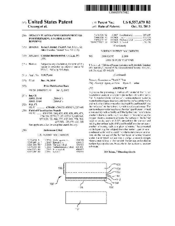
 Alex Usenko