This article has been accepted for publication in a future issue of this journal, but has not been fully edited. Content may change prior to final publication. Citation information: DOI 10.1109/JLT.2018.2877461, Journal of
Lightwave Technology
> REPLACE THIS LINE WITH YOUR PAPER IDENTIFICATION NUMBER (DOUBLE-CLICK HERE TO EDIT) <
1
Real-Time and DSP-free 128 Gb/s PAM-4 Link
using a Binary Driven Silicon Photonic
Transmitter
Jochem Verbist, Joris Lambrecht, Michiel Verplaetse, Srinivasan Ashwyn Srinivasan, Peter De Heyn,
Timothy De Keulenaer, Rames Pierco, Arno Vyncke, Joris Van Campenhout, Xin Yin,
Johan Bauwelinck, Guy Torfs and Gunther Roelkens
Abstract— Optical transmitters for four-level pulse amplitude
modulation (PAM-4) have attracted a significant amount of
research in recent years, in large part due to the standardization
of the format for the 200 and 400 Gigabit Ethernet (GbE) optical
interconnects in data centers. However, combining low-power and
linear operation of the electro-optical frontend with sufficiently
large bandwidths has proven challenging, especially for the 100
Gb/s/λ links (i.e. employing 50 Gbaud PAM-4). The most
straightforward solution has been to deal with the non-idealities of
the modulator in the electrical domain: predistorting the signal
levels and/or equalizing the frequency response with the help of
digital signal processing (DSP). However, this typically requires
fast DACs, either capable of delivering large swings (>1 Vpp) or
supplemented with an additional linear amplifier to drive the
optical modulator. Both options substantially increase the power
consumption and the complexity of the transceiver. Rather than
allocating effort to linearize the electrical to optical conversion of
a single modulator, we propose a topology that performs the DAC
operation in the optical domain. Two compact electro-absorption
modulators (EAMs) in an interferometer layout are driven with
NRZ data to generate the four-level signal in the optical domain.
Using this topology, we demonstrate the first real-time 128 Gb/s
PAM-4 transmission with a silicon photonic transmitter in a chipto-chip link. In a back-to-back setup, we obtained a bit-error ratio
(BER) of 4×10⁻¹⁰ without requiring any DAC, DSP, or modulators
with large traveling wave structures. Over 1 km of standard single
mode fiber a BER of 8×10⁻⁶ is recorded, still well below the KP4
forward error-coding limit. These results correspond to the lowest
BERs reported for any real-time PAM-4 link at 100 Gb/s or
higher, illustrating the benefit of performing the DAC operation
in the optical domain.
Index Terms—PAM-4, short-reach interconnects, silicon
photonics
This paragraph of the first footnote will contain the date on which you
submitted your paper for review. It will also contain support information,
including sponsor and financial support acknowledgment
J. Verbist is with IDLab, Ghent University—IMEC, Department of
Information Technology, Ghent 9052, Belgium. He is also with the Photonics
Research Group, Ghent University—IMEC, Department of Information
Technology, Ghent 9052, Belgium (e-mail: jochem.verbist@ugent.be).
J. Lambrecht, M. Verplaetse, J. Van Kerrebrouck, X. Yin, G. Torfs, and
J. Bauwelinck are with IDLab, the Ghent University—IMEC, Department of
Information Technology, Ghent 9052, Belgium (e-mail: {joris.lambrecht;
I. INTRODUCTION
T
HE recent adoption of the 400 Gigabit Ethernet (GbE)
standards has made four-level pulse amplitude modulation
(PAM-4) the modulation format of choice for the nextgeneration single-mode data center interconnects (DCI). The
400GBASE standard specifies 8 lanes of 53.125 Gb/s PAM-4
for 1 km and 2 km standard single-mode fiber (SSMF) links and
4 lanes of 106.25 Gb/s PAM-4 for 500m SSMF links,
introducing the first 100 Gb/s per wavelength standard [1].
However, also for longer fiber spans a 4x100G PAM-4 scheme
is a likely candidate, as it offers the lowest practical lane count
and thus the most compact transceiver. Regardless of the
outcome of these ongoing standardizations, the wide spread
deployment of 100G-per- modules remains a logical step on
the growth path of data centers, irrespective of the interconnect
span. Possibly an even more challenging task is updating the
copper interconnects to sustain these rapidly increasing data
rates. Moreover, with the increasing data rates next-generation
optical interconnects are expected to move to the intra-rack and
intra-board interconnects [2]. Especially for these on-board
optical interconnects, minimizing power and area (both
electrically and optically) will be of the utmost importance.
Previously, several examples of 100G-per- PAM-4 links
have been demonstrated [3-11]. However, many of these
examples had to rely on DACs, ADCs, and/or digital signal
processing (DSP) at the transmitter and/or at the receiver [510], leading to a significant increase in latency, power
consumption, and cost. Often the required DSP at the receiver
prevents online (or real-time) link experiments, even with highend test equipment. Nevertheless, some real-time examples
demonstrating 100 Gb/s single-lane PAM-4 transmission have
michiel.verplaetse;
joris.vankerrebrouck;
xin.yin;
guy.torfs;
johan.bauwelinck}@ugent.be).
G. Roelkens is with the Photonics Research Group, Ghent University—
IMEC, Department of Information Technology, Ghent 9052, Belgium (e-mail:
gunther.roelkens@ugent.be).
S. A. Srinivasan, P. De Heyn and J. Van Campenhout are with IMEC,
Leuven 3001, Belgium (e-mail: {ashwyn.srinivasan; Peter.DeHeyn;
joris.vancampenhout}@imec.be).
T. De Keulenaer is with BiFAST, Ghent 9000, Belgium (e-mail: {timothy;
ramses; arno }@bifast.io)
(c) 2018 IEEE. Personal use of this material is permitted.
0733-8724 (c) 2018 IEEE. Personal use is permitted, but republication/redistribution requires IEEE permission. See http://www.ieee.org/publications_standards/publications/rights/index.html for more information.
�This article has been accepted for publication in a future issue of this journal, but has not been fully edited. Content may change prior to final publication. Citation information: DOI 10.1109/JLT.2018.2877461, Journal of
Lightwave Technology
> REPLACE THIS LINE WITH YOUR PAPER IDENTIFICATION NUMBER (DOUBLE-CLICK HERE TO EDIT) <
(a)
2
(b)
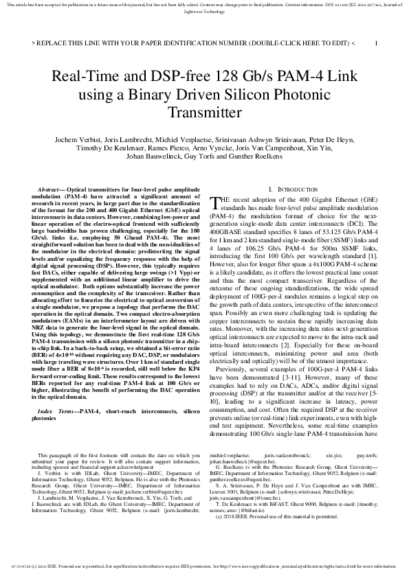
Fig. 1. (a) 2-bit optical DAC consisting of two intensity modulators (EAMs). (b) Vector and eye diagrams of the proposed topology optical PAM-4 generator.
The blue vectors represent the on- and off-state of the two EAMs, when driven separately (assuming for simplicity that no phase difference is introduced between
the 0 and the 1 level by the EAMs). They form the basis vectors for the PAM-4 generation and realize a rectangular constellation in the upper quadrant of the
complex plane. The limited extinction ratio (ER of 10 dB in this example) and the resulting non-perfect zero level, are represented by the dotted vectors. As long
as the 90° angle is preserved between both vectors, the ER does not influence the relative positioning of the power levels, only the maximal modulation depth of
the PAM-4. Even if the EAMs behave as non-perfect switches (limited ER, unbalanced IL, non-zero average phase-shift), PAM-4 can still properly be generated
by adjusting the phase and/or power split. Vice versa, these parameters can also be used to predistort the PAM-4 levels (e.g. to compensate for compression in
the receiver). A more in-depth discussion can be found in [11].
been reported [3,4]. In [3], real-time 56 Gbaud PAM-4
transmission on a discrete LiNbO3 Mach-Zehnder modulator
(MZM) was reported. The first real-time demonstration using
a polymer on silicon MZM at 53.125 Gbaud was shown in [4],
with online DSP. Both experiments employ large travelling
wave modulators (at least several millimeters long) and
consequently need to be electrically terminated (typically with
a 50Ω resistor), consuming a significant amount of power and
transceiver real-estate.
In this paper, we use a novel optical PAM-4 generator based
on two binary driven GeSi electroabsorption modulators
(EAMs) in an interferometer topology, as we recently
demonstrated in [11]. As the EAMs are only 120 µm long, they
can be driven lumped without any travelling wave electrodes or
terminations. Combining this modulator with an in-house
developed transceiver chipset, we are able to demonstrate the
first real-time, single-wavelength transmission of 128 Gb/s
PAM-4 in a chip-to-chip link. Bit-error ratios (BERs)
comfortably below the KP4 forward error coding (FEC) limit
of 2.4 ⋅ 10 are obtained for spans up to 1 km of SSMF,
without requiring any power-hungry DACs, ADCs or DSP.
II. OPTICAL PAM-4 GENERATION
As all high-speed optical modulators are characterized by a
non-linear transfer function, the most straightforward solution
has been to compensate these non-idealities in the electrical
domain by predistorting the levels of the applied PAM-4 signal
and/or by equalizing the frequency response of the electrooptical channel. Although this solution can be very effective in
leveraging non-ideal electrical and optical components, it
comes at a substantial increase in the total power consumption,
size, and complexity of the transceiver.
Rather than allocating transceiver resources in linearizing the
electrical-to-optical conversion of a single intensity modulator,
we propose to postpone the DAC operation until the optical
domain by using two parallel intensity modulators [11]. This
Fig. 2. Two different versions of the optical PAM-4 generator using two
parallel EAMs in an interferometer with 90° phase difference: (left) using an
unequal optical power split and (right) using an unequal drive voltage.
To achieve equidistant PAM-4 with either of these topologies, the OMA
(optical modulation amplitude) of the MSB needs to be twice the OMA of the
LSB, when driven separately. This condition translates to (left) a 66:33 power
ratio or (right) a 1: β voltage swing ratio (β < 1, with β=0.5 for a linear EAM)
between the MSB and the LSB EAM. Although both version generate
equidistant PAM-4, they do not have the same efficiency. Comparing the eye
diagrams produced by both versions, we see that the optical power split always
produces a OMA that is 33% better (or 1.25 dB higher) than the OMA of the
voltage weighted version, for a given modulator and average input power
(Pavg).
removes the linearity requirements at the transmit side, both in
the optics and the electronics. Adding a second modulator
means we also need to provide a second modulator driver. Still,
two NRZ drivers are likely to be more power efficient than one
multilevel driver. Both drivers can be designed for non-linear
operation, allowing other driver topologies to be considered
(e.g. inverters) and maintaining compatibility with CMOSbased electronics and all the advantages that come with it.
Recently, we proposed a topology consisting of two intensity
modulators in interferometer with 90° phase difference, where
0733-8724 (c) 2018 IEEE. Personal use is permitted, but republication/redistribution requires IEEE permission. See http://www.ieee.org/publications_standards/publications/rights/index.html for more information.
�This article has been accepted for publication in a future issue of this journal, but has not been fully edited. Content may change prior to final publication. Citation information: DOI 10.1109/JLT.2018.2877461, Journal of
Lightwave Technology
> REPLACE THIS LINE WITH YOUR PAPER IDENTIFICATION NUMBER (DOUBLE-CLICK HERE TO EDIT) <
3
Fig. 3. Experiment setup for the 128 Gb/s PAM-4 link
the LSB/MSB coding is realized through a 33:66 power ratio
between both branches (Fig.1.a) [11]. Fig.1.b provides a more
detailed explanation of the optical DAC operation using a
vector diagram drawn in the first quadrant of the complex plane.
The EAMs are 120µm long GeSi-based devices fabricated on
imec’s 200mm platform. Their operation is based on the FranzKeldysh effect. The bandgap of the material shifts when an
electrical field is applied, changing its optical absorption
spectrum. More information about on these GeSi devices can
be found in [12,13]. EAMs have the advantage that they can be
made very short (minimizing the modulator capacitance and
allowing them to be driven as a small lumped capacitor),
removing the need for long transmission lines and powerconsuming resistive terminations. However, to be able to drive
the EAMs with commercially available 50 Ω-drivers (i.e. RF
amplifiers), we have placed 50Ω resistors between the
bondpads of each modulator to provide a matched interface on
the PIC. These resistors are not necessary for the operation of
the transmitter and can easily be omitted when integrated with
a dedicated driver. Moreover, we recently demonstrated that
such a dedicated driver for these type of EAMs can be made
extremely power efficient, consuming only 61 mW at 70 Gb/s
or less than 0.9 pJ/bit [14].
These first generation devices are implemented with standard
1x2 multimode interferometers with equal power split, both at
the input and at the output of the interferometer. Therefore, the
LSB/MSB weighing between both branches can be achieved by
reducing the voltage swing to the LSB-EAM, as illustrated in
Fig. 2. In the experiment setup, shown in Fig. 3, a 6 dB
attenuator was placed after one of the RF amplifiers. Due to the
non-linear characteristics of the EAMs this does not perfectly
correspond to a 3 dB lower optical modulation amplitude in the
LSB arm. Additional corrections are applied by slightly
adjusting the bias voltage of the LSB-EAM. However, this
emulation only approximates the intended PAM-4 generation,
resulting in slightly unequal PAM-4 levels and reducing the
overall performance. With a 33:66 power split the transmitter
eye levels would be perfectly equidistant if both modulators
were driven with the same voltage swing, no matter their
specific transfer function (assuming no parasitic phase shift is
introduced between the 0 and the 1 by the EAM) [11]. This
33:66 power split can easily be accomplished by replacing one
of the MMIs with a tunable Mach-Zehnder interferometer (e.g.
consisting of two MMIs and a thermal phase shifter). Moreover,
Fig. 2 also shows that the version with unequal power split will
always be more efficient than version with unequal drive
voltage version. For a given modulator, maximum drive voltage
and optical input power, the power split version produces a
PAM-4 with a 1.25 dB higher OMA. A micrograph of the used
photonic IC (PIC) with equal power split can be seen in Fig.4.
An in-house developed transmitter (TX-IC in Fig.4) is used
to multiplex four 16 Gb/s pseudo-random bit streams (PRSB),
originating from the FPGA, into one serial 64 Gb/s 29-1 long
PRBS signal. After the MUX, an analog 6-tap feed-forward
equalizer can be set to improve the frequency response of the
following components in the channel. In our experiments, it was
mainly used to compensate the strong frequency roll-off of the
electrical receiver and the RF amplifier. The differential outputs
of the TX-IC are decorrelated with a mechanically tunable time
delay to provide independent 64 Gb/s NRZs streams to each
modulator. Finally, the signals are externally amplified to
1.1Vpp and 2.2Vpp for the LSB and the MSB EAM,
respectively. The voltage swing could be slightly higher than in
the previous experiments on similar devices [11] as the device
is permitted to operate non-linearly, allowing the EAMs to be
operated as switches for maximal ER. Light from a 10 dBm
laser at 1567nm is coupled in and out of the PIC though fiberto-chip grating couplers with an insertion loss of
approximately 5.5 dB/coupler. The EAMs have an estimated
insertion loss of 8 dB and a dynamic extinction ratio of
approximately 10 dB, resulting in an average in-fiber power
around -10 dBm during operation.
III. REAL-TIME PAM-4 BER TESTER
Using a transmitter as discussed in the previous section
allows us to generate open PAM-4 eyes up to 64 Gbaud without
any DSP, thanks to the optical DAC topology. However,
receiving these signals in real-time is particularly challenging
as a commercial 64 Gbaud PAM-4 bit-error rate tester (BERT)
did not yet exist at the time of the experiments. Real-time
oscilloscopes are not an option as the captured data has to be
saved and processed offline. Still, even with a fast enough
0733-8724 (c) 2018 IEEE. Personal use is permitted, but republication/redistribution requires IEEE permission. See http://www.ieee.org/publications_standards/publications/rights/index.html for more information.
�This article has been accepted for publication in a future issue of this journal, but has not been fully edited. Content may change prior to final publication. Citation information: DOI 10.1109/JLT.2018.2877461, Journal of
Lightwave Technology
> REPLACE THIS LINE WITH YOUR PAPER IDENTIFICATION NUMBER (DOUBLE-CLICK HERE TO EDIT) <
Fig. 4. Photograph and block diagram of the BiCMOS transmitter IC (TXIC), the BiCMOS receiver IC (RX-IC), and an annotated die micropgraph of
the silicon photonic modulator. More details about the TX-IC and RX-IC can
be found in [15].
BERT it is often difficult to estimate what the performance of
the link would be without any high-end test equipment.
Therefore, we implemented a custom electrical receiver
using an in-house developed chip (RX-IC) that was originally
designed to decode a 3-level duobinary signal [15]. Fig. 4
shows the block diagram of the RX-IC as well as a photograph
of the die mounted on a high-speed printed circuit board. The
receiver consists of two comparators to monitor the upper and
lower triangular duobinary eyes. Their outputs are XOR-ed to
reproduce the original binary data and finally deserialized to a
quarter-rate NRZ signal. Fig.5 explains how two of these
receivers can be used to obtain both the most and least
significant bit (MSB and LSB) of the PAM-4 signal
simultaneously. This is in contrast to the few currently available
solutions, where each of the three eyes is evaluated sequentially
and the three BERs are averaged.
The received PAM-4 signal is split 50:50 and fed to two
photodectors, one for each RX-IC. Both photodetectors have a
similar responsivity (~0.6 A/W) and a flat frequency response
(important to prevent any signal distortion when converting to
the electrical domain) up to 40 and 50 GHz. Alternatively, we
could have opted to split the signal after the conversion in the
electrical domain, saving one photodiode. However, as the RXIC only provides a demultiplexed and retimed output, the
second photodiode could be used to monitor the eye diagram
during the optimization of the equalizer settings for optimal
BER (i.e. the BER of the MSB or the LSB depending on which
photodiode is being monitored). As no linear high-speed
transimpedance amplifier (TIA) was available, an erbiumdoped fiber amplifier (EDFA) was used to provide a sufficiently
large signal at the inputs of the RX-ICs. The EDFA can be
omitted by replacing the relatively inefficient grating couplers
with low-loss edge couplers (< 2 dB/coupler) and adding a TIA.
4
Fig. 5. Implementation of the real-time PAM-4 receiver with automatic Gray
code demapper and bit-error rate tester (BERT).
Decoding the MSB is relatively straightforward, as the
duobinary receiver can be easily reduced to a conventional
binary receiver by setting the threshold VTH1 to its highest
possible level, making the XOR operation transparent for the
second comparator. The MSB is then received by centering
VTH2 around the DC-level, looking into the middle eye.
To decode the LSB, each comparator of RX-IC 2 is set to the
middle of one of the outer eyes. However, the outer eyes by
themselves do not provide sufficient information to decide the
received LSB. It is instructive to think of a duobinary receiver
as a device determining if a symbol transition happened inside
(delivering a 1) or outside (delivering a 0) both comparator
thresholds. Combining this information with that of the MSB
(i.e. has a symbol transition happened in the upper or lower half
of the eye), resolves exactly which eye of the three has seen a
symbol transition and therefor the LSB. Lastly, to obtain the
LSB we need to XOR it once more with the MSB. However,
we purposefully omit this operation as the receiver now also
performs an automatic demapping of a Gray encoded PAM-4
symbol, making this an additional advantage of this receiver
topology, as Gray mapping and demapping is a required action
set by most data center transceiver standards. Furthermore, in a
test setup one can choose to Gray code the transmitted data or
not, as this does not affect the BER performance when
transmitting PRBS data. As both the MSB and the LSB are
essentially two equal length PRSB streams, XOR-ing both will
produce again an equivalent PRBS stream on which the BER
counter (implemented on the FPGA) can lock.
IV. RESULTS AND DISCUSSION
The stand-alone performance of the transmitter is first
assessed by connecting one of the photodiodes directly to a 50
GHz sampling oscilloscope and tuning the equalizers settings
towards best eye quality. The heater was detuned slightly to
0733-8724 (c) 2018 IEEE. Personal use is permitted, but republication/redistribution requires IEEE permission. See http://www.ieee.org/publications_standards/publications/rights/index.html for more information.
�This article has been accepted for publication in a future issue of this journal, but has not been fully edited. Content may change prior to final publication. Citation information: DOI 10.1109/JLT.2018.2877461, Journal of
Lightwave Technology
> REPLACE THIS LINE WITH YOUR PAPER IDENTIFICATION NUMBER (DOUBLE-CLICK HERE TO EDIT) <
Fig. 6. Eye diagrams at 64 GBaud in the back-to-back case and after
transmission over 500 m and 1 km of standard single mode fiber. An eye
diagram with a GeSi EAM used as photodetector (back-to-back) is also shown.
produce a smaller phase difference, increasing the OMA of the
upper eye without reducing that of other eyes as described in
[11]. As long as the receiver is not limited in dynamic range,
this effect can be used to improve the BER. Fig. 6 shows the
eye diagrams in the back-to-back (B2B) case and after
transmission over 500 m and 1 km of standard single mode
fiber. Clear open eyes are obtained for all links. Next, the
photodiode is connected again to the RX-IC to evaluate the realtime BER performance. The FFE parameters have to be reoptimized to minimize the BER, indicating that frequency
response of the RX-ICs indeed limits the link performance.
Furthermore, as the receiver was designed for 3-level duobinary
reception, it did not need to be extremely linear. For example a
symmetrical, gradually saturating transfer function would
suffice to decode duobinary without experiencing large
sensitivity penalties. Nevertheless, for PAM-4 almost error-free
operation was obtained in a back-to-back link with BERs down
to 4×10⁻¹⁰. For transmission over 500m and 1 km of SSMF we
measured BERs of 7×10⁻⁹ and 8×10⁻⁶, respectively, which is
well below the KP4-FEC limit of 2.4×10⁻⁴ commonly used in
data center interconnects, as shown in Fig. 7. These BERs are
to the lowest reported values for a real-time PAM-4 link above
50 Gbaud [9,10]. This affirms once more the performance
benefit of the DAC-less solution over a single multilevel driven
modulator as was previously observed for the modulator used
in this experiment [11], as well as for other optical DACs such
as segmented MZMs [7] and polarization multiplexed EAMs
[17].
Apart from their compact form factor and high bandwidth,
the EAMs can also be used as photodetectors by setting them to
maximal absorption. In [15,16], we already observed that the
EAMs can be used as optical receivers for 100 Gb/s NRZ and
3-level duobinary with a high responsivity (~0.8 A/W for 80µm
devices). However, to receive PAM-4, the frequency response
should ideally be as flat as possible. We can compare the
performance by switching the transmitted eye between the
photodiode with a known flat response beyond 50 GHz (upper
left eye diagram in Fig.6) and one of the transmitter EAMs
biased at -3V on a separate die (lower right eye diagram in Fig.
6). Apart from some additional noise, likely due the added
insertion loss of the extra grating coupler and 3dB-splitter, little
5
Fig. 7. Real-time BER curves at 64 Gbaud for back-to-back, 500m and 1km
of SSMF.
or no additional signal degradation is observed. This validates
that the EAMs not only have a high responsivity but also a flat
frequency response up to at least 50 GHz, making them wellsuited for receiving multilevel signals. Having a single active
high-speed optical component for both the transmitter and the
receiver, would greatly simplify the yield optimization of such
a silicon-based transceiver, paving the way towards high-yield
and high-volume production.
Silicon photonics is very promising platform for data center
interconnects, due to its ability to realize compact and low-cost
transceivers in high volume leveraging existing CMOS
fabrication infrastructure. As demonstrated in this paper, SiP is
capable of delivering very compact transceivers that can
operated without the need for DSP, DACs or high-power
electronics. The next step would be to combine this modulator
with in-house developed dedicated drivers [14] and TIA[18],
and realize a low power analog fronted of a silicon transceiver
with a dynamic power consumption of less than 2.5pJ/bit
(excluding the laser): 61 mW to drive the MSB EAM, 45 mW
for the LSB (as it needs half the swing), 10-20 mW for the
heater and 190 mW for the TIA.
The main downside of silicon-on-insulator (SOI) platform is
that lacks a native means for optical amplification, and as such
no light source. However, many possible solutions exist [19]:
lasers can be grown epitaxially on the SOI (heterogeneous
integration) or butt-coupled to the PIC during assembly without
having to interfere with the SOI. Recently, transfer printing has
gained quite some attention as a promising and -most
importantly- cost-effective way to selectively transfer pieces of
III-V material (e.g. a laser) to a SOI wafer or PIC. The same
technique could be used to replace the GeSi EAMs with III-Vbased EAMs to allow operation in O-band, as the GeSi FranzKeldysh effect devices are intrinsically limited to C- and Lband. Another option would be the use of O-band waveguideintegrated EAMs on silicon based on the quantum-confined
Stark effect through multiple quantum well structures, as are
currently being developed [20]. However, the proposed optical
DAC topology is not limited to EAMs, in fact any intensity
modulator could be used.
0733-8724 (c) 2018 IEEE. Personal use is permitted, but republication/redistribution requires IEEE permission. See http://www.ieee.org/publications_standards/publications/rights/index.html for more information.
�This article has been accepted for publication in a future issue of this journal, but has not been fully edited. Content may change prior to final publication. Citation information: DOI 10.1109/JLT.2018.2877461, Journal of
Lightwave Technology
> REPLACE THIS LINE WITH YOUR PAPER IDENTIFICATION NUMBER (DOUBLE-CLICK HERE TO EDIT) <
V. CONCLUSION
We have presented a compact silicon-based transmitter
capable of generating 64 Gbaud PAM-4 using two binary
driven 120 μm long GeSi EAMs in parallel. Combined with an
in-house developed electrical transceiver chipset, we were able
to demonstrate the first real-time 64 Gbaud PAM-4
transmission over more than 1 km of SSMF in a chip-to-chip
link, without requiring any power-hungry electrical ADCs,
DACs or DSP. Integration with the custom-designed BiCMOS
drivers of [14] would allow us to realize a 1 pJ/bit transmitter
frontend (excluding the laser). These results not only illustrate
the advantages of carrying out the DAC operation to the optical
domain and thus eliminating the need for linear electronics and
optics, but also the capabilities of silicon photonics towards
realizing extremely compact and low-power transceivers for
100 Gb/s/λ optical interconnects.
REFERENCES
[1]
[2]
[3]
[4]
[5]
[6]
[7]
[8]
[9]
[10]
[11]
[12]
[13]
[14]
[15]
“IEEE P802.3bs 400 Gigabit Ethernet Task Force.” [Online]. Available:
http://www.ieee802.org/3/bs/
Consortium
for
On-Board
Optics
(COBO),
[Online]
https://onboardoptics.org
M. Chagnon, M. Osman, M. Poulin, C. Latrasse, J. Gagné, Y. Painchaud,
C. Paquet, S. Lessard, and D. Plant, "Experimental study of 112 Gb/s
short reach transmission employing PAM formats and SiP intensity
modulator at 1.3 μm," Opt. Express 22, 21018-21036 (2014).
M. A. Mestre et al., "Compact InP-Based DFB-EAM Enabling PAM-4
112 Gb/s Transmission Over 2 km," in Journal of Lightwave Technology,
vol. 34, no. 7, pp. 1572-1578, April 1, 1 2016.
Justin Lavrencik, Varghese Antony Thomas, Siddharth Varughese, and
Stephen E. Ralph, "DSP-Enabled 100 Gb/s PAM-4 VCSEL MMF
Links," J. Lightwave Technol. 35, 3189-3196 (2017)
W. Wang et al., "First Demonstration of 112 Gb/s PAM-4 Amplifier-free
Transmission over a Record Reach of 40 km Using 1.3 μm Directly
Modulated Laser," 2018 Optical Fiber Communications Conference and
Exposition (OFC), San Diego, CA, 2018, pp. 1-3.
Alireza Samani, David Patel, Mathieu Chagnon, Eslam El-Fiky, Rui Li,
Maxime Jacques, Nicolás Abadía, Venkat Veerasubramanian, and David
V. Plant, "Experimental parametric study of 128 Gb/s PAM-4
transmission system using a multi-electrode silicon photonic Mach
Zehnder modulator," Opt. Express 25, 13252-13262 (2017)
J. Sun et al., "A 128 Gb/s PAM4 Silicon Microring Modulator," 2018
Optical Fiber Communications Conference and Exposition (OFC), San
Diego, CA, 2018, pp. 1-3.
J. Lee et al., "Demonstration of 112-Gbit/s optical transmission using
56GBaud PAM-4 driver and clock-and-data recovery ICs," ECOC, 2015,
Valencia, 2015, pp. 1-3.
A. Chiuchiarelli et al., "Single Wavelength 100G Real-Time
Transmission for High-speed Data Center Communications," in OFC,
2017, Los Angeles, W4I.2.
J. Verbist et al., "DAC-Less and DSP-Free 112 Gb/s PAM-4 Transmitter
Using Two Parallel Electroabsorption Modulators," in Journal of
Lightwave Technology, vol. 36, no. 5, pp. 1281-1286, March1, 1 2018.
M. Pantouvaki et al., "Active Components for 50 Gb/s NRZ-OOK
Optical Interconnects in a Silicon Photonics Platform," in Journal of
Lightwave Technology, vol. 35, no. 4, pp. 631-638, Feb.15, 15 2017.
S. A. Srinivasan, P. Verheyen, R. Loo, I. D. Wolf, M. Pantouvaki, G.
Lepage, S. Balakrishnan, W. Vanherle, P. Absil, and J. V.
Campenhout,“50 Gb/s C-band GeSi Waveguide Electro-Absorption
Modulator,” in 2016 Optical Fiber Communications Conference and
Exhibition (OFC), March 2016, pp. 1–3.
H. Ramon et al. , “70 Gb/s 0.87 pJ/bit GeSi EAM Driver in 55nm SiGe
BiCMOS”, 2018 European Conference on Optical Communication
(ECOC), Rome, 2018, Tu3E.5 (to be published)
J. Verbist et al., "Real-Time 100 Gb/s NRZ and EDB Transmission With
a GeSi Electroabsorption Modulator for Short-Reach Optical
Interconnects," in JLT, vol. 36, no. 1, pp. 90-96, Jan. 2018.
6
[16] J. Verbist et al., "100 Gb/s DAC-less and DSP-free Transmitters using
GeSi EAMs for Short-Reach Optical Interconnects," 2018 Optical Fiber
Communications Conference and Exposition (OFC), San Diego, CA,
2018, pp. 1-3.
[17] W. Huang et al., "Optical DAC for Generation of PAM4 Using Parallel
Electro-Absorption Modulators," ECOC (2016), Dusseldorf, Germany,
pp. 1-3
[18] J. Lambrecht et al. “56-Gb/s Silicon Optical Receiver using a Low-Noise
Fully-Differential Transimpedance Amplifier in SiGe BiCMOS”, in
ECOC ( 2018), Rome, Tu3E.6 (to be published)
[19] Z. Wang et al., “Novel Light Source Integration Approaches for Silicon
Photonics” in Laser & Photonics Reviews, 11: 1700063, 2017
[20] A. Srinivasan, C. Porret, E. Vissers, P. Geiregat, D. Van Thourhout, R.
Loo, M. Pantouvaki, J. Van Campenhout, "High-contrast quantumconfined Stark effect in Ge/SiGe quantum well stacks on Si with ultrathin buffer layers", Conference on Lasers and Electro-Optics Pacific
Rim, (2018).
Jochem Verbist received a B.Sc. degree in Electrical
Engineering from Ghent University, Belgium, in 2011
and M.Sc. degree in 2013. Since 2014, he has been
pursuing a joint Ph.D. degree in Electrical Engineering
with both the IDLab Design group and the Photonics
Research Group, Ghent University-INTEC-Imec,
Belgium, as part of the GOA– electronic/photonic
integration platform. His current research focuses on
low-power silicon transceivers for short-reach optical
interconnects and the electronic/photonic co-design of
electronic drivers for high speed optical telecom/datacom/5G systems.
Joris Lambrecht was born in Ghent, Belgium, in 1992.
He received the M.S. Degree in electrical engineering
from Ghent University, Belgium, in 2015, where he is
currently working towards the Ph.D. degree. He has been
a Research Assistant in the IDLab Design group, Ghent
University, since 2015. His research focusses on highspeed optical receiver design.
Michiel Verplaetse was born in Ghent, Belgium, in
1993. He graduated in electrical engineering from
Ghent University, Belgium, in 2016. In the same year
he joined the IDLab Design group at Ghent University
where he is currently working toward a Ph.D. degree.
His technical interests are mixed signal circuit design,
mainly focusing on equalization structures.
Srinivasan Ashwyn Srinivasan has completed his
doctoral studies on advanced Ge devices for optical
interconnect applications at University of Ghent and
imec. He also received his Master’s degree on Micro
and Nanotechnologies for Integrated systems from
Swiss Federal Institute of Technology Lausanne,
Grenoble INP and Politecnico di Torino with La
Mention Tres Bien and 110/110 con lode. He also
holds a Bachelor of Technology degree on Electronics
and Communication Engineering from National
Institute of Technology Tiruchirappalli, India. Currently he is a R&D Photonics
0733-8724 (c) 2018 IEEE. Personal use is permitted, but republication/redistribution requires IEEE permission. See http://www.ieee.org/publications_standards/publications/rights/index.html for more information.
�This article has been accepted for publication in a future issue of this journal, but has not been fully edited. Content may change prior to final publication. Citation information: DOI 10.1109/JLT.2018.2877461, Journal of
Lightwave Technology
> REPLACE THIS LINE WITH YOUR PAPER IDENTIFICATION NUMBER (DOUBLE-CLICK HERE TO EDIT) <
and Device Integration engineer at imec working on next generation active
photonic devices for improved optical link power efficiency and bandwidth
density. His research interests lies at the confluence of optics, communication,
electronics and computation.
Peter De Heyn biography not available at time of publication
Timothy De Keulenaer is currently working at BiFAST,
a spin-off of Ghent University IDLab. He received the
M.Sc. and Ph.D. degree in applied electronical
engineering from Ghent University, Ghent, Belgium, in
2010 and 2015 respectively. His main interests are highspeed BiCMOS integrated circuit design for 112Gb/s and
signal integrity aspects for back-plane communication.
He is the (co-) inventor of three duobinary related patents
and currently focuses on the development of serial
interconnects to enable serial data rates of 112 Gb/s
within cloud data centers.
Ramses Pierco is currently working at BiFAST, a spinoff of Ghent University IDLab. He received the master
degree in applied electrical engineering from Ghent
University, Belgium in 2010 and has from then on been
working at the INTEC Design laboratory part of the
department of information technology at Ghent
University. There he received the PhD degree in applied
electrical engineering in 2015. He is currently
responsible for the technology development within
BiFAST in which his focus lies on further integration of
a BiCMOS chipset aiming at data rates ranging from 40 Gb/s up to 112 Gb/s.
Arno Vyncke is currently working at BiFAST, a spin-off
of Ghent University IDLab. He received the M.Sc. and
Ph.D. degree in applied electronical engineering from
Ghent University, Ghent, Belgium, in 2010 and 2016
respectively. His research is focused on clock and data
recovery circuits for next generation low-power passive
optical networks. His focus within BiFAST is on the
digital part of ICs for serial interconnects enabling highspeed data center connectivity, as well as operations
management.
7
Johan Bauwelinck received a Ph.D. degree in applied
sciences, electronics from Ghent University, Belgium
in 2005. Since Oct. 2009, he is a professor in the
INTEC department at the same university and since
2014 he is leading the IDLab Design group. His
research focuses on high-speed, high-frequency (opto) electronic circuits and systems, and their applications
on chip and board level, including transmitter and
receiver analog front-ends for wireless, wired and
fiber-optic communication or instrumentation
systems. He was and is active in the EU-funded projects GIANT, POWERNET,
PIEMAN, EuroFOS, C3- PO, Mirage, Phoxtrot, Spirit, Flex5Gware, Teraboard,
Streams and WIPE conducting research on advanced electronic integrated
circuits for next generation transport, metro, access, datacenter and radio-overfiber networks. He has promoted 18 PhDs and co-authored more than 150
publications and 10 patents in the field of high-speed electronics and fiber-optic
communication. He is a member of the ECOC technical program committee.
Guy Torfs (S’07 M’13) received the M.S. and Ph.D.
degree in electrical engineering from Ghent University,
Belgium, in 2007 and 2012, respectively. From 2007 on,
he has been working at the INTEC design laboratory
associated with imec and part of the Department of
Information Technology at Ghent University. His
research focuses on highspeed mixed signal designs for
wireless baseband and fiber-optic and backplane
communication systems, including digital signal
processing and calibration, analog equalization circuits
and clock and data recovery systems.
Gunther Roelkens received a degree in electrical
engineering from Ghent University, Belgium, in 2002
and a PhD from the same university in 2007, at the
Department of Information Technology (INTEC),
where he is currently full professor. In 2008, he was a
visiting scientist in IBM TJ Watson Research Center,
New York. His research interest includes the
heterogeneous integration of III-V semiconductors
and other materials on top of silicon waveguide
circuits and electronic/photonic co-integration. He
was holder of an ERC starting grant (MIRACLE), to start up research in the
field of integrated mid-infrared photonic integrated circuits.
Xin Yin (M’06) received the B.E. and M.Sc. degrees in
electronics engineering from the Fudan University,
Shanghai, China, in 1999 and 2002, respectively, and
the Ph.D. degree in applied sciences, electronics from
Ghent University, Ghent, Belgium, in 2009. Since 2007,
he has worked as a staff researcher in IMEC-INTEC and
since 2013 he has been a professor in the INTEC
department at Ghent University. His current research
interests include high-speed and high-sensitive optoelectronic circuits and subsystems, with emphasis on
burst-mode receiver and CDR/EDC for optical access networks, and low-power
mixed-signal integrated circuit design for telecom/datacom/5G/IoT
applications. He led a team which won the GreenTouch 1000x award together
with Bell Labs/Alcatel-Lucent and Orange Labs in Nov. 2014.
Joris Van Campenhout biography not available at time of publication
0733-8724 (c) 2018 IEEE. Personal use is permitted, but republication/redistribution requires IEEE permission. See http://www.ieee.org/publications_standards/publications/rights/index.html for more information.
�
 Peter De Heyn