WO2025147410A2 - Electrophoretic media comprising a cationic charge control agent - Google Patents
Electrophoretic media comprising a cationic charge control agent Download PDFInfo
- Publication number
- WO2025147410A2 WO2025147410A2 PCT/US2024/061641 US2024061641W WO2025147410A2 WO 2025147410 A2 WO2025147410 A2 WO 2025147410A2 US 2024061641 W US2024061641 W US 2024061641W WO 2025147410 A2 WO2025147410 A2 WO 2025147410A2
- Authority
- WO
- WIPO (PCT)
- Prior art keywords
- group
- formula
- represented
- charge control
- electrophoretic medium
- Prior art date
- Legal status (The legal status is an assumption and is not a legal conclusion. Google has not performed a legal analysis and makes no representation as to the accuracy of the status listed.)
- Pending
Links
Classifications
-
- C—CHEMISTRY; METALLURGY
- C09—DYES; PAINTS; POLISHES; NATURAL RESINS; ADHESIVES; COMPOSITIONS NOT OTHERWISE PROVIDED FOR; APPLICATIONS OF MATERIALS NOT OTHERWISE PROVIDED FOR
- C09B—ORGANIC DYES OR CLOSELY-RELATED COMPOUNDS FOR PRODUCING DYES, e.g. PIGMENTS; MORDANTS; LAKES
- C09B67/00—Influencing the physical, e.g. the dyeing or printing properties of dyestuffs without chemical reactions, e.g. by treating with solvents grinding or grinding assistants, coating of pigments or dyes; Process features in the making of dyestuff preparations; Dyestuff preparations of a special physical nature, e.g. tablets, films
- C09B67/0033—Blends of pigments; Mixtured crystals; Solid solutions
-
- C—CHEMISTRY; METALLURGY
- C09—DYES; PAINTS; POLISHES; NATURAL RESINS; ADHESIVES; COMPOSITIONS NOT OTHERWISE PROVIDED FOR; APPLICATIONS OF MATERIALS NOT OTHERWISE PROVIDED FOR
- C09K—MATERIALS FOR MISCELLANEOUS APPLICATIONS, NOT PROVIDED FOR ELSEWHERE
- C09K9/00—Tenebrescent materials, i.e. materials for which the range of wavelengths for energy absorption is changed as a result of excitation by some form of energy
- C09K9/02—Organic tenebrescent materials
-
- G—PHYSICS
- G02—OPTICS
- G02F—OPTICAL DEVICES OR ARRANGEMENTS FOR THE CONTROL OF LIGHT BY MODIFICATION OF THE OPTICAL PROPERTIES OF THE MEDIA OF THE ELEMENTS INVOLVED THEREIN; NON-LINEAR OPTICS; FREQUENCY-CHANGING OF LIGHT; OPTICAL LOGIC ELEMENTS; OPTICAL ANALOGUE/DIGITAL CONVERTERS
- G02F1/00—Devices or arrangements for the control of the intensity, colour, phase, polarisation or direction of light arriving from an independent light source, e.g. switching, gating or modulating; Non-linear optics
- G02F1/01—Devices or arrangements for the control of the intensity, colour, phase, polarisation or direction of light arriving from an independent light source, e.g. switching, gating or modulating; Non-linear optics for the control of the intensity, phase, polarisation or colour
- G02F1/165—Devices or arrangements for the control of the intensity, colour, phase, polarisation or direction of light arriving from an independent light source, e.g. switching, gating or modulating; Non-linear optics for the control of the intensity, phase, polarisation or colour based on translational movement of particles in a fluid under the influence of an applied field
- G02F1/166—Devices or arrangements for the control of the intensity, colour, phase, polarisation or direction of light arriving from an independent light source, e.g. switching, gating or modulating; Non-linear optics for the control of the intensity, phase, polarisation or colour based on translational movement of particles in a fluid under the influence of an applied field characterised by the electro-optical or magneto-optical effect
- G02F1/167—Devices or arrangements for the control of the intensity, colour, phase, polarisation or direction of light arriving from an independent light source, e.g. switching, gating or modulating; Non-linear optics for the control of the intensity, phase, polarisation or colour based on translational movement of particles in a fluid under the influence of an applied field characterised by the electro-optical or magneto-optical effect by electrophoresis
-
- G—PHYSICS
- G02—OPTICS
- G02F—OPTICAL DEVICES OR ARRANGEMENTS FOR THE CONTROL OF LIGHT BY MODIFICATION OF THE OPTICAL PROPERTIES OF THE MEDIA OF THE ELEMENTS INVOLVED THEREIN; NON-LINEAR OPTICS; FREQUENCY-CHANGING OF LIGHT; OPTICAL LOGIC ELEMENTS; OPTICAL ANALOGUE/DIGITAL CONVERTERS
- G02F1/00—Devices or arrangements for the control of the intensity, colour, phase, polarisation or direction of light arriving from an independent light source, e.g. switching, gating or modulating; Non-linear optics
- G02F1/01—Devices or arrangements for the control of the intensity, colour, phase, polarisation or direction of light arriving from an independent light source, e.g. switching, gating or modulating; Non-linear optics for the control of the intensity, phase, polarisation or colour
- G02F1/165—Devices or arrangements for the control of the intensity, colour, phase, polarisation or direction of light arriving from an independent light source, e.g. switching, gating or modulating; Non-linear optics for the control of the intensity, phase, polarisation or colour based on translational movement of particles in a fluid under the influence of an applied field
- G02F1/1675—Constructional details
- G02F1/16757—Microcapsules
-
- G—PHYSICS
- G02—OPTICS
- G02F—OPTICAL DEVICES OR ARRANGEMENTS FOR THE CONTROL OF LIGHT BY MODIFICATION OF THE OPTICAL PROPERTIES OF THE MEDIA OF THE ELEMENTS INVOLVED THEREIN; NON-LINEAR OPTICS; FREQUENCY-CHANGING OF LIGHT; OPTICAL LOGIC ELEMENTS; OPTICAL ANALOGUE/DIGITAL CONVERTERS
- G02F1/00—Devices or arrangements for the control of the intensity, colour, phase, polarisation or direction of light arriving from an independent light source, e.g. switching, gating or modulating; Non-linear optics
- G02F1/01—Devices or arrangements for the control of the intensity, colour, phase, polarisation or direction of light arriving from an independent light source, e.g. switching, gating or modulating; Non-linear optics for the control of the intensity, phase, polarisation or colour
- G02F1/165—Devices or arrangements for the control of the intensity, colour, phase, polarisation or direction of light arriving from an independent light source, e.g. switching, gating or modulating; Non-linear optics for the control of the intensity, phase, polarisation or colour based on translational movement of particles in a fluid under the influence of an applied field
- G02F1/1675—Constructional details
- G02F1/1679—Gaskets; Spacers; Sealing of cells; Filling or closing of cells
- G02F1/1681—Gaskets; Spacers; Sealing of cells; Filling or closing of cells having two or more microcells partitioned by walls, e.g. of microcup type
-
- C—CHEMISTRY; METALLURGY
- C09—DYES; PAINTS; POLISHES; NATURAL RESINS; ADHESIVES; COMPOSITIONS NOT OTHERWISE PROVIDED FOR; APPLICATIONS OF MATERIALS NOT OTHERWISE PROVIDED FOR
- C09K—MATERIALS FOR MISCELLANEOUS APPLICATIONS, NOT PROVIDED FOR ELSEWHERE
- C09K2211/00—Chemical nature of organic luminescent or tenebrescent compounds
- C09K2211/10—Non-macromolecular compounds
- C09K2211/1003—Carbocyclic compounds
-
- G—PHYSICS
- G02—OPTICS
- G02F—OPTICAL DEVICES OR ARRANGEMENTS FOR THE CONTROL OF LIGHT BY MODIFICATION OF THE OPTICAL PROPERTIES OF THE MEDIA OF THE ELEMENTS INVOLVED THEREIN; NON-LINEAR OPTICS; FREQUENCY-CHANGING OF LIGHT; OPTICAL LOGIC ELEMENTS; OPTICAL ANALOGUE/DIGITAL CONVERTERS
- G02F1/00—Devices or arrangements for the control of the intensity, colour, phase, polarisation or direction of light arriving from an independent light source, e.g. switching, gating or modulating; Non-linear optics
- G02F1/01—Devices or arrangements for the control of the intensity, colour, phase, polarisation or direction of light arriving from an independent light source, e.g. switching, gating or modulating; Non-linear optics for the control of the intensity, phase, polarisation or colour
- G02F1/165—Devices or arrangements for the control of the intensity, colour, phase, polarisation or direction of light arriving from an independent light source, e.g. switching, gating or modulating; Non-linear optics for the control of the intensity, phase, polarisation or colour based on translational movement of particles in a fluid under the influence of an applied field
- G02F1/1675—Constructional details
- G02F2001/1678—Constructional details characterised by the composition or particle type
Definitions
- This invention relates to electrophoretic media for electro-optic devices, the electrophoretic media comprising a plurality of charged pigment particles and a cationic charge control agent in a non-polar liquid.
- the molecular structure of the charge control agent includes two quaternary ammonium functional groups, two or more amide functional groups or two or more ester functional groups, and two or more aliphatic biradical units, each of the two or more aliphatic biradical units comprising a ring structure.
- Particle-based electrophoretic displays have been the subject of intense research and development for a number of years.
- a plurality of charged pigment particles (sometimes referred to as charged particles or pigment particles) move through a fluid under the influence of an electric field.
- the electric field is typically provided by a conductive film or a transistor, such as a field-effect transistor.
- Electrophoretic displays have good brightness and contrast, wide viewing angles, state bistability, and low power consumption when compared with liquid crystal displays. Such electrophoretic displays have slower switching speeds than LCD displays, however, and electrophoretic displays are typically too slow to display real-time video. Additionally, the electrophoretic displays can be sluggish at low temperatures because the viscosity of the fluid limits the movement of the charged pigment particles.
- electrophoretic displays can be found in everyday products such as electronic books (e-readers), mobile phones and mobile phone covers, smart cards, signs, watches, shelf labels, and flash drives.
- solid electro-optic displays include rotating bichromal member displays, encapsulated electrophoretic displays, microcell electrophoretic displays and encapsulated liquid crystal displays.
- bistable and “bistability” are used herein in their conventional meaning in the art to refer to displays comprising display elements having first and second display states differing in at least one optical property, and such that after any given element has been driven, by means of an addressing pulse of finite duration, to assume either its first or second display state, after the addressing pulse has terminated, that state will persist for at least several times, for example at least four times, the minimum duration of the addressing pulse required to change the state of the display element.
- addressing pulse of finite duration
- some particle-based electrophoretic displays capable of gray scale are stable not only in their extreme black and white states but also in their intermediate gray states, and the same is true of some other types of electro-optic displays.
- This type of display is properly called “multi-stable” rather than bistable, although for convenience the term “bistable” may be used herein to cover both bistable and multi-stable displays.
- Encapsulated electrophoretic media comprise numerous small capsules, each of which itself comprises an electrophoretic medium containing electrophoretically-mobile pigment particles in a fluid medium, and a capsule wall surrounding the electrophoretic medium.
- the capsules are themselves held within a polymeric binder to form a coherent layer positioned between two electrodes.
- microcell electrophoretic display In a microcell electrophoretic display, the charged pigment particles and the fluid are not encapsulated within microcapsules but instead are retained within a plurality of cavities formed within a carrier medium, typically a polymeric film.
- a carrier medium typically a polymeric film.
- Electrophoretic particles, fluids and fluid additives see for example U.S.
- electrophoretic media are often opaque (since, for example, in many electrophoretic media, the charged pigment particles substantially block transmission of visible light through the display) and operate in a reflective mode
- many electrophoretic displays can be made to operate in a so-called "shutter mode" in which one display state is substantially opaque and one is light-transmissive. See, for example, U.S. Patents Nos. 5,872,552; 6,130,774; 6,144,361; 6,172,798; 6,271,823; 6,225,971; and 6,184,856.
- Di electrophoretic displays which are similar to electrophoretic displays but rely upon variations in electric field strength, can operate in a similar mode; see U.S. Patent No. 4,418,346.
- Electro-optic media operating in shutter mode may be useful in multi-layer structures for full color displays; in such structures, at least one layer adjacent the viewing surface of the display operates in shutter mode to expose or conceal a second layer more distant from the viewing surface.
- An encapsulated electrophoretic display typically does not suffer from the clustering and settling failure mode of traditional electrophoretic devices and provides further advantages, such as the ability to print or coat the display on a wide variety of flexible and rigid substrates.
- printing is intended to include all forms of printing and coating, including, but without limitation: pre-metered coatings such as patch die coating, slot or extrusion coating, slide or cascade coating, curtain coating; roll coating such as knife over roll coating, forward and reverse roll coating; gravure coating; dip coating; spray coating; meniscus coating; spin coating; brush coating; air knife coating; silk screen printing processes; electrostatic printing processes; thermal printing processes; ink jet printing processes; electrophoretic deposition (See U.S. Patent No. 7,339,715); and other similar techniques.)
- pre-metered coatings such as patch die coating, slot or extrusion coating, slide or cascade coating, curtain coating
- roll coating such as knife over roll coating, forward and reverse roll coating
- gravure coating dip coating
- spray coating meniscus coating
- spin coating brush coating
- An electrophoretic display normally comprises a layer of electrophoretic material and at least two other layers disposed on opposed sides of the electrophoretic material, one of these two layers being an electrode layer.
- both the layers are electrode layers, and one or both of the electrode layers are patterned to define the pixels of the display.
- one electrode layer may be patterned into elongate row electrodes and the other into elongate column electrodes running at right angles to the row electrodes, the pixels being defined by the intersections of the row and column electrodes.
- one electrode layer has the form of a single continuous electrode, and the other electrode layer is patterned into a matrix of pixel electrodes, each of which defines one pixel of the display.
- electrophoretic display which is intended for use with a stylus, print head or similar movable electrode separate from the display
- only one of the layers adjacent the electrophoretic layer comprises an electrode, the layer on the opposed side of the electrophoretic layer typically being a protective layer intended to prevent the movable electrode damaging the electrophoretic layer.
- the manufacture of a three-layer electrophoretic display normally involves at least one lamination operation.
- a process for manufacturing an encapsulated electrophoretic display in which an encapsulated electrophoretic medium comprising capsules in a binder is coated on to a flexible substrate comprising indium-tin-oxide (ITO) or a similar conductive coating (which acts as one electrode of the final display) on a plastic film, the capsules/binder coating being dried to form a coherent layer of the electrophoretic medium firmly adhered to the substrate.
- ITO indium-tin-oxide
- a similar conductive coating which acts as one electrode of the final display
- a backplane containing an array of pixel electrodes and an appropriate arrangement of conductors to connect the pixel electrodes to drive circuitry, is prepared.
- the substrate having the capsule/binder layer thereon is laminated to the backplane using a lamination adhesive.
- a lamination adhesive A very similar process can be used to prepare an electrophoretic display usable with a stylus or similar movable electrode by replacing the backplane with a simple protective layer, such as a plastic film, over which the stylus or other movable electrode can slide.
- the backplane is itself flexible and is prepared by printing the pixel electrodes and conductors on a plastic film or other flexible substrate.
- electrophoretic displays may make use of an active matrix backplane comprising an array of transistors or diodes and a corresponding array of pixel electrodes, and a "continuous" front electrode (in the sense of an electrode which extends over multiple pixels and typically the whole display) on a transparent substrate, these components being essentially the same as in LCD's.
- LCDs are normally assembled by forming the backplane and front electrode on separate glass substrates, then adhesively securing these components together leaving a small aperture between them, placing the resultant assembly under vacuum, and immersing the assembly in a bath of the liquid crystal, so that the liquid crystal flows through the aperture between the backplane and the front electrode. Finally, with the liquid crystal in place, the aperture is sealed to provide the final display.
- This LCD assembly process cannot readily be transferred to encapsulated displays. Because the electrophoretic material is solid, it must be present between the backplane and the front electrode before these two integers are secured to each other. Furthermore, in contrast to a liquid crystal material, which is simply placed between the front electrode and the backplane without being attached to either, an encapsulated electrophoretic medium normally needs to be secured to both; in most cases the electrophoretic medium is formed on the front electrode, since this is generally easier than forming the medium on the circuitry-containing backplane, and the front el ectrode/ electrophoretic medium combination is then laminated to the backplane, typically by covering the entire surface of the electrophoretic medium with an adhesive and laminating under heat, pressure and possibly vacuum.
- Electro-optic displays can be costly; for example, the cost of the color LCD found in a portable computer is typically a substantial fraction of the entire cost of the computer. As the use of such displays spreads to devices, such as cellular telephones and personal digital assistants (PDA's), much less costly than portable computers, there is great pressure to reduce the costs of such displays.
- PDA's personal digital assistants
- An electro-optic display normally comprises a layer of electro-optic material and at least two other layers disposed on opposed sides of the electro-optic material, one of these two layers being an electrode layer.
- both the layers are electrode layers, and one or both of the electrode layers are patterned to define the pixels of the display.
- one electrode layer may be patterned into elongate row electrodes and the other into elongate column electrodes running at right angles to the row electrodes, the pixels being defined by the intersections of the row and column electrodes.
- one electrode layer has the form of a single continuous electrode, and the other electrode layer is patterned into a matrix of pixel electrodes, each of which defines one pixel of the display.
- electro-optic display which is intended for use with a stylus, print head or similar movable electrode separate from the display
- only one of the layers adjacent the electrooptic layer comprises an electrode, the layer on the opposed side of the electro-optic layer typically being a protective layer intended to prevent the movable electrode damaging the electro-optic layer.
- the aforementioned U.S. Patent No. 6,982,178 describes a method of assembling a solid electro-optic display (including an encapsulated electrophoretic display) which is well adapted for mass production.
- this patent describes a so-called "front plane laminate" ("FPL") which comprises, in order, a light-transmissive electrically-conductive layer; a layer of a solid electro-optic medium in electrical contact with the electrically- conductive layer; an adhesive layer; and a release sheet.
- FPL front plane laminate
- the light-transmissive electrically-conductive layer will be carried on a light-transmissive substrate, which is preferably flexible, in the sense that the substrate can be manually wrapped around a drum (say) 10 inches (254 mm) in diameter without permanent deformation.
- the term "light- transmissive" is used in this patent and herein to mean that the layer thus designated transmits sufficient light to enable an observer, looking through that layer, to observe the change in display states of the electro-optic medium, which will normally be viewed through the electrically-conductive layer and adjacent substrate (if present); in cases where the electrooptic medium displays a change in reflectivity at non-visible wavelengths, the term “light- transmissive” should of course be interpreted to refer to transmission of the relevant non-visible wavelengths.
- the substrate will typically be a polymeric film and will normally have a thickness in the range of about 1 to about 25 mil (25 to 634 m), preferably about 2 to about 10 mil (51 to 254 pm).
- the electrically-conductive layer is conveniently a thin metal or metal oxide layer of, for example, aluminum or ITO, or may be a conductive polymer.
- PET poly(ethylene terephthalate)
- PET poly(ethylene terephthalate)
- Mylar is a Registered Trademark
- E.I. du Pont de Nemours & Company Wilmington DE, and such commercial materials may be used with good results in the front plane laminate.
- U.S. Patent No. 7,561,324 describes a so-called "double release sheet" which is essentially a simplified version of the front plane laminate of the aforementioned U.S. Patent No. 6,982,178.
- One form of the double release sheet comprises a layer of a solid electro-optic medium sandwiched between two adhesive layers, one or both of the adhesive layers being covered by a release sheet.
- Another form of the double release sheet comprises a layer of a solid electro-optic medium sandwiched between two release sheets.
- Both forms of the double release film are intended for use in a process generally similar to the process for assembling an electro-optic display from a front plane laminate already described, but involving two separate laminations; typically, in a first lamination the double release sheet is laminated to a front electrode to form a front sub-assembly, and then in a second lamination the front sub-assembly is laminated to a backplane to form the final display, although the order of these two laminations could be reversed if desired.
- U. S. Patent No. 7,839,564 describes a so-called "inverted front plane laminate", which is a variant of the front plane laminate described in the aforementioned U.S. Patent No. 6,982,178.
- This inverted front plane laminate comprises, in order, at least one of a light- transmissive protective layer and a light-transmissive electrically-conductive layer; an adhesive layer; a layer of a solid electro-optic medium; and a release sheet.
- This inverted front plane laminate is used to form an electro-optic display having a layer of lamination adhesive between the electro-optic layer and the front electrode or front substrate; a second, typically thin layer of adhesive may or may not be present between the electro-optic layer and a backplane.
- Such electro-optic displays can combine good resolution with good low temperature performance.
- Electrooptic media can be used as coatings on windows (including skylights and sunroofs) to enable the proportion of incident radiation transmitted through the windows to be electronically controlled by varying the optical state of the electro-optic media.
- Effective implementation of such "variable-transmissivity" (“VT") technology in buildings is expected to provide
- each of the red, green, blue, and white primaries occupy one fourth of the display area (one sub-pixel out of four), with the white sub-pixel being as bright as the underlying monochrome display white, and each of the colored sub-pixels being no lighter than one third of the monochrome display white.
- the brightness of the white color shown by the display as a whole cannot be more than one half of the brightness of the white sub-pixel. This is caused by the fact that white areas of the display are produced by displaying the one white sub-pixel out of each four, plus each colored sub-pixel in its colored form being equivalent to one third of a white sub-pixel.
- the three colored sub-pixels combined contribute no more than the one white sub-pixel.
- Each of the two or more aliphatic biradical units may be selected from the group consisting of molecular structures that are represented by Formula I and Formula II.
- the molecular structure of the charge control agent may comprise a group that is represented by Formula III, wherein each Q is independently selected from the group consisting of oxygen and NH group, wherein each -Z- is independently selected from the group consisting of an aliphatic biradical unit -A- and an aliphatic biradical unit -B-, -A- being represented by Formula I, and -B- being represented by Formula II, and wherein r is an integer from 1 to 20.
- the molecular structure of the charge control agent may be represented by Formula IV, wherein Rl, R2, and R3 are independently selected by the group consisting of an alkyl, aryl, and alkenyl group, wherein each Q is independently selected from the group consisting of oxygen and NH group, wherein each -Z- is independently selected from the group consisting of an aliphatic biradical unit -A- and an aliphatic biradical unit -B-, -A- being represented by Formula I, and -B- being represented by Formula II, and wherein r is an integer from 1 to 20.
- Rl, R2, and R3 are independently selected by the group consisting of an alkyl, aryl, and alkenyl group, wherein each Q is independently selected from the group consisting of oxygen and NH group, wherein each -Z- is independently selected from the group consisting of an aliphatic biradical unit -A- and an aliphatic biradical unit -B-, -A- being represented by
- the molecular structure of the charge control agent may be represented by Formula V, wherein Rl, R2, and R3 are independently selected by the group consisting of alkyl, aryl, and alkenyl group, wherein each Q is independently selected from the group consisting of oxygen, and NH group, wherein each G is independently selected from the group consisting of oxygen, sulfur, and NH group, wherein D is -(CH2)t -, where t is an integer from 3 to 6, wherein each -Z- is independently selected from the group consisting of an aliphatic biradical unit -A- and an aliphatic biradical unit -B-, -A- being represented by Formula I, and -B- being represented by Formula II, and wherein r is an integer from 1 to 20.
- Rl, R2, and R3 are independently selected by the group consisting of alkyl, aryl, and alkenyl group
- each Q is independently selected from the group consisting of oxygen, and NH group
- each G is independently selected from
- the molecular structure of the charge control agent may be represented by Formula V, wherein Rl, R2, R3 are methyl, G is oxygen or NH, Q is oxygen, D is -(CH2)s-, and -Z- is an aliphatic biradical unit that is represented by Formula I or Formula II.
- the molecular structure of the charge control agent may be represented by Formula V, wherein Rl, R2, R3 are methyl, G is oxygen or NH, and -Z- is an aliphatic biradical unit that is represented by Formula I.
- the molecular structure of the charge control agent may be represented by Formula V, wherein Rl, R2, R3 are methyl, G is oxygen or NH, and -Z- is an aliphatic biradical unit that is represented by Formula I.
- the molecular structure of the charge control agent may be represented by Formula V, wherein Rl, R2, R3 are methyl, G is oxygen or NH, and -Z- is an aliphatic biradical unit that is
- the molecular structure of the charge control agent may be represented by Formula
- the charge control agent may have a weight average molecular weight greater than or equal to 1000 g/mol or from 1000 g/mol to 8,000 g/mol.
- the electrophoretic medium of the present invention may also comprise a second charge control agent.
- the second charge control agent may comprise a hydrophobic moiety and a head group selected from the group comprising an anionic functional group, a nonionic functional group, and a cationic functional group.
- the plurality of charged pigment particles may be capable of moving through the non-polar liquid upon application of an electric field.
- the electrophoretic medium of the present invention may comprise a plurality of first, second, and third types of charged pigment particles, wherein each type of charged pigment particles has different color from each other type of charged pigment particles.
- the plurality of charged pigment particles are capable of moving through the non-polar liquid upon application of an electric field.
- the electrophoretic medium of the present invention may further comprise a plurality of fourth type of charged pigment particles, each of the plurality of fourth type of charged pigment particles having different color from each particle from the pluralities of first, second and third type of charged pigment particles.
- Each particle of the plurality of the first and second types of charged pigment particles may have a negative charge, whereas each particle of the plurality of the third and fourth types of charged pigment particles may have a positive charge.
- Each particle of the plurality of first type of charged pigment particles may have a first charge polarity, whereas each particle of the plurality of the second, third and fourth types of charged pigment particles may have a second charge polarity, the second charge polarity being opposite from the first charge polarity.
- the molecular structure of the charge control agent may be represented by Formula IV, wherein Rl, R2, and R3 are independently selected by the group consisting of an alkyl, aryl, and alkenyl group, wherein each Q is independently selected from the group consisting of oxygen and NH group, wherein each -Z- is independently selected from the group consisting of an aliphatic biradical unit -A- and an aliphatic biradical unit -B-, -A- being represented by Formula I, and -B- being represented by Formula II, and wherein r is an integer from 1 to 20.
- the molecular structure of the charge control agent may be represented by Formula V, wherein Rl, R2, and R3 are independently selected by the group consisting of alkyl, aryl, and alkenyl group, wherein each Q is independently selected from the group consisting of oxygen, and NH group, wherein each G is independently selected from the group consisting of oxygen, sulfur, and NH group, wherein D is -(CH2)t -, where t is an integer from 3 to 6, wherein each -Z- is independently selected from the group consisting of an aliphatic biradical unit -A- and an aliphatic biradical unit -B-, -A- being represented by Formula I, and -B- being represented by Formula II, and wherein r is an integer from 1 to 20.
- Rl, R2, and R3 are independently selected by the group consisting of alkyl, aryl, and alkenyl group
- each Q is independently selected from the group consisting of oxygen, and NH group
- each G is independently selected from
- FIG. 1 is a side view of a color electro-optic display comprising electrophoretic medium encapsulated in microcapsules.
- the color electrophoretic display comprises, in order, a first electrode layer, an electro-optic material layer, a first adhesive layer, and a second electrode layer.
- FIG. 2 is a side view of a color electro-optic display comprising electrophoretic medium encapsulated in microcapsules.
- the color electrophoretic display comprises, in order, a first electrode layer, a second adhesive layer, an electro-optic material layer, a first adhesive layer, and a second electrode layer.
- FIG. 3 is a side view of a color electro-optic display comprising electrophoretic medium encapsulated in microcells.
- the color electrophoretic display comprises, in order, a first electrode layer, an electro-optic material layer including a sealing layer, a first adhesive layer, and a second electrode layer.
- FIG. 4 is a graph of the color gamut of an electro-optic display that comprises an inventive electrophoretic medium and a graph of the color gamut of an electro-optic display that comprises a comparative electrophoretic medium.
- the present invention provides electrophoretic media comprising charged pigment particles, a charge control agent, and a non-polar liquid.
- a particle that absorbs, scatters, or reflects light, either in a broad band or at selected wavelengths, is referred to herein as a colored or pigment particle.
- the electrophoretic media may be incorporated into displays, or into front plane laminates or inverted front plane laminates, front plane laminates and inverted front plane laminates being coupled to a backplane to form a display.
- head group of a molecule that comprises both a hydrophilic and hydrophobic part is the functional group of the hydrophilic part of the molecule.
- the molecule may have one group or more than one head groups.
- MW molecular weight
- aliphatic biradical unit is a molecular structure, which is part of a larger molecule, wherein the molecular structure of the biradical unit has two or more terminal atoms, each of the two or more terminal atoms being bonded to another molecular fragment or functional group to form a larger molecule. That is, the larger molecule that contains the “aliphatic biradical unit”, such as the charge control agent in this instance, does not contain a single electron species (reactive free radicals).
- the literature occasionally refers to an ethylene group -CH2CH2- (or a methylene group -CH2-) as a biradical, even if it is part of a molecule such as ethylene chloride (CI-CH2CH2-CI), which does not contain any radicals at its non-excited state.
- CI-CH2CH2-CI ethylene chloride
- the terminal atoms of the biradical units are carbon atom s (part of the terminal -CH2- groups).
- the electrophoretic media comprises a plurality of charged pigment particles, a charge control agent, and a nonpolar liquid.
- the charge control agent has a molecular structure that includes two or more quaternary ammonium functional groups, two or more amide functional groups or two or more ester functional groups, and two or more aliphatic biradical units, each of the two or more aliphatic biradical unit comprising a ring structure.
- Each of the two or more aliphatic biradical units may contain from 28 to 40 carbon atoms
- Quaternization An amount of 86.50 g of the isolated polymeric mixture was mixed with 50.0 g of toluene and stirred under nitrogen. An amount of 1.107 g of dimethyl sulfate was added and the mixture was stirred at ambient temperature to complete the quaternization reaction. The product was vacuum stripped to remove volatiles yielding quatemized polymer. This type of quaternized polymer is generally represented by Formula V.
- An electrophoretic medium was prepared using white, cyan, magenta, and yellow charged pigment particles, charge control agent from Comparative Example 1, and Isopar E. White charged pigment particles were negatively charged, whereas cyan, magenta, and yellow charged pigment particles were positively charged. The electrophoretic medium was used to prepare an electro-optic display illustrated in FIG. 3.
- An electrophoretic medium was prepared using white, cyan, magenta, and yellow charged pigment particles, charge control agent from Example 2, and Isopar E. White charged pigment particles were negatively charged, whereas cyan, magenta, and yellow charged pigment particles were positively charged. The electrophoretic medium was used to prepare an electro-optic display illustrated in FIG. 3.
- Each of the electro-optic displays from Comparative Example 3 and Example 4 was electrically driven to generate various optical states at 25°C, the reflection spectra of which were acquired using a spectrophotometer.
- CIE L*, a* and b* values of the reflected light from each electrophoretic display were measured.
- the minimum distance in L*a*b* space of the color of the display from each of the eight SNAP (Specifications for Newsprint Advertising Production) color standard primaries was calculated in units of AE*.
- the full color gamut from all measured points was also extracted.
- the primary colors were red, green, blue, yellow, cyan, magenta, white, and black (R, G, B, Y, C, M, W, and K).
- FIG. 4 The results of color gamut of Inventive and Comparative Examples are summarized in FIG. 4.
- the solid line of figure corresponds to the gamut of inventive electro-optic display from Ex. 4 and the wide dotted line of the figure corresponds to the gamut of the Comparative electro-optic display form Ex. 3, wherein the narrow-dotted line of the figures corresponds to the color standard (SNAP).
- the electrophoretic medium comprising the inventive charge control agent provided a broader total color gamut volume (58,100) compared to the system containing the control charge control agent (45,000).
- the improved performance of the inventive charge control agent is achieved because of the presence of (a) two cationic groups (quaternary ammonium groups) and (b) the branched alkyl groups in the molecular structure of the charge control agent.
- Such structures may provide reverse micelles with loops of branched hydrophobic groups on their surface, increasing the micelle stability in the non-polar liquid of the electrophoretic medium.
- the branched structure of the inventive charge control agent is expected to improve its solubility and its low temperature electro-optic performance even at low temperatures.
Landscapes
- Physics & Mathematics (AREA)
- Nonlinear Science (AREA)
- Chemical & Material Sciences (AREA)
- General Physics & Mathematics (AREA)
- Optics & Photonics (AREA)
- Chemical Kinetics & Catalysis (AREA)
- Organic Chemistry (AREA)
- Health & Medical Sciences (AREA)
- Life Sciences & Earth Sciences (AREA)
- Electrochemistry (AREA)
- Molecular Biology (AREA)
- Materials Engineering (AREA)
- Engineering & Computer Science (AREA)
- Electrochromic Elements, Electrophoresis, Or Variable Reflection Or Absorption Elements (AREA)
Abstract
Electrophoretic media are disclosed containing a plurality of charged pigment particles, a charge control agent, and a non-polar liquid. The molecular structure of the charge control agent includes two quaternary ammonium functional groups, two or more amide functional groups or two or more ester functional groups, and two or more aliphatic biradical units, each of the two or more aliphatic biradical units comprising a ring structure.
Description
Electrophoretic Media Comprising a Cationic Charge Control Agent
RELATED APPLICATIONS
[0001] This application claims priority to U.S. Provisional Patent Application No. 63/616,957 filed on January 2, 2024, which is incorporated by reference in its entirety, along with all other patents and patent applications disclosed herein.
FIELD OF THE INVENTION
[0002] This invention relates to electrophoretic media for electro-optic devices, the electrophoretic media comprising a plurality of charged pigment particles and a cationic charge control agent in a non-polar liquid. The molecular structure of the charge control agent includes two quaternary ammonium functional groups, two or more amide functional groups or two or more ester functional groups, and two or more aliphatic biradical units, each of the two or more aliphatic biradical units comprising a ring structure.
BACKGROUND OF THE INVENTION
[0003] The term "electro-optic", as applied to a material or a display, is used herein in its conventional meaning in the imaging art to refer to a material having first and second display states differing in at least one optical property, the material being changed from its first to its second display state by application of an electric field to the material. Although the optical property is typically color perceptible to the human eye, it may be another optical property, such as optical transmission, reflectance, luminescence or, in the case of displays intended for machine reading, pseudo-color in the sense of a change in reflectance of electromagnetic wavelengths outside the visible range.
[0004] Particle-based electrophoretic displays have been the subject of intense research and development for a number of years. In such displays, a plurality of charged pigment particles (sometimes referred to as charged particles or pigment particles) move through a fluid under the influence of an electric field. The electric field is typically provided by a conductive film or a transistor, such as a field-effect transistor. Electrophoretic displays have good brightness and contrast, wide viewing angles, state bistability, and low power consumption when compared with liquid crystal displays. Such electrophoretic displays have slower switching speeds than LCD displays, however, and electrophoretic displays are typically too slow to display real-time video. Additionally, the electrophoretic displays can be sluggish at low temperatures because the viscosity of the fluid limits the movement of the charged pigment particles. Despite these shortcomings, electrophoretic displays can be found in everyday
products such as electronic books (e-readers), mobile phones and mobile phone covers, smart cards, signs, watches, shelf labels, and flash drives.
[0005] The term "gray state" is used herein in its conventional meaning in the imaging art to refer to a state intermediate two extreme optical states of a pixel and does not necessarily imply a black-white transition between these two extreme states. For example, several of the E Ink patents and published applications referred to below describe electrophoretic displays in which the extreme states are white and deep blue, so that an intermediate "gray state" would be pale blue. Indeed, as already mentioned, the change in optical state may not be a color change at all. The terms "black" and "white" may be used hereinafter to refer to the two extreme optical states of a display and should be understood as normally including extreme optical states which are not strictly black and white, for example the aforementioned white and dark blue states. The term "monochrome" may be used hereinafter to denote a drive scheme which only drives pixels to their two extreme optical states with no intervening gray states.
[0006] Many commercial electrophoretic media essentially display only two colors, with a gradient between the black and white extremes, known as “grayscale”. Such electrophoretic media either use a single type of electrophoretic particle having a first color in a colored fluid having a second, different color, or first and second types of charged pigment particles having different first and second colors in an uncolored fluid. In the former case, the first color is displayed when the charged pigment particles lie adjacent the viewing surface of the display and the second color is displayed when the charged pigment particles are spaced from the viewing surface. In the latter case, the first color is displayed when the first type of charged pigment particles lie adjacent the viewing surface of the display and the second color is displayed when the second type of charged pigment particles lie adjacent the viewing surface. Typically, the two colors are black and white.
[0007] Some electro-optic materials are solid in the sense that the materials have solid external surfaces, although the materials may, and often do, have internal liquid- or gas-filled spaces. Such displays using solid electro-optic materials may hereinafter for convenience be referred to as "solid electro-optic displays". Thus, the term "solid electro-optic displays" includes rotating bichromal member displays, encapsulated electrophoretic displays, microcell electrophoretic displays and encapsulated liquid crystal displays.
[0008] The terms "bistable" and "bistability" are used herein in their conventional meaning in the art to refer to displays comprising display elements having first and second display states differing in at least one optical property, and such that after any given element has been driven, by means of an addressing pulse of finite duration, to assume either its first or second display
state, after the addressing pulse has terminated, that state will persist for at least several times, for example at least four times, the minimum duration of the addressing pulse required to change the state of the display element. It is shown in U.S. Patent No. 7,170,670 that some particle-based electrophoretic displays capable of gray scale are stable not only in their extreme black and white states but also in their intermediate gray states, and the same is true of some other types of electro-optic displays. This type of display is properly called "multi-stable" rather than bistable, although for convenience the term "bistable" may be used herein to cover both bistable and multi-stable displays.
[0009] One type of electro-optic display, which has been the subject of intense research and development for a number of years, is the particle-based electrophoretic display, in which a plurality of charged pigment particles move through a fluid under the influence of an electric field. Electrophoretic displays can have attributes of good brightness and contrast, wide viewing angles, state bistability, and low power consumption when compared with liquid crystal displays. Nevertheless, problems with the long-term image quality of these displays have prevented their widespread usage. For example, charged pigment particles that make up electrophoretic displays tend to settle, resulting in inadequate service-life for these displays.
[0010] Numerous patents and applications assigned to or in the names of the Massachusetts Institute of Technology (MIT), E Ink Corporation, E Ink California, LLC. and related companies describe various technologies used in encapsulated and microcell electrophoretic and other electro-optic media. Encapsulated electrophoretic media comprise numerous small capsules, each of which itself comprises an electrophoretic medium containing electrophoretically-mobile pigment particles in a fluid medium, and a capsule wall surrounding the electrophoretic medium. Typically, the capsules are themselves held within a polymeric binder to form a coherent layer positioned between two electrodes. In a microcell electrophoretic display, the charged pigment particles and the fluid are not encapsulated within microcapsules but instead are retained within a plurality of cavities formed within a carrier medium, typically a polymeric film. [[Hereinafter, the term "microcavity electrophoretic display" may be used to cover both encapsulated and microcell electrophoretic displays. ]]The technologies described in these patents and applications include:
[0011] (a) Electrophoretic particles, fluids and fluid additives; see for example U.S.
Patents Nos. 5,961,804; 6,017,584; 6,120,588; 6,120,839; 6,262,706; 6,262,833; 6,300,932; 6,323,989; 6,377,387; 6,515,649; 6,538,801; 6,580,545; 6,652,075; 6,693,620; 6,721,083;
6,727,881; 6,822,782; 6,831,771; 6,870,661; 6,927,892; 6,956,690; 6,958,849; 7,002,728;
7,038,655; 7,052,766; 7,110,162; 7,113,323; 7,141,688; 7,142,351; 7,170,670; 7,226,550;
7,230,750; 7,230,751; 7,236,290; 7,277,218; 7,286,279; 7,312,916; 7,382,514; 7,390,901;
7,473,782; 7,561,324; 7,583,251; 7,572,394; 7,576,904; 7,580,180; 7,679,814; 7,848,006;
7,903,319; 8,018,640; 8,115,729; 8,257,614; 8,270,064; 8,363,306; 8,390,918; 8,582,196;
8,654,436; 8,902,491; 8,961,831; 9,052,564; 9,341,915; 9,348,193; 9,361,836; 9,366,935;
9,372,380; 9,382,427; 9,423,666; 9,428,649; 9,557,623; 9,670,367; 9,671,667; 9,688,859;
9,726,957; 9,752,034; 9,765,015; 9,778,535; 9,778,537; 9,835,926; 9,953,588; 9,995,987;
10,025,157; 10,031,394; 10,040,954; 10,061,123; 10,062,337; 10,147,366; and 10,514,583; and U.S. Patent Application Publication Nos. 2003/0048522; 2003/0151029; 2003/0164480; 2004/0030125; 2004/0105036; 2005/0012980; 2009/0009852; 2011/0217639; 2012/0049125; 2013/0161565; 2013/0193385; 2013/0244149; 2013/0063333; 2014/0011913; 2014/0078576; 2014/0104674; 2014/0231728; 2015/0177590; 2015/0185509; 2015/0241754; 2015/0301425; and 2016/0170106;
[0012] (b) Capsules, binders and encapsulation processes; see for example U.S. Patents
Nos. 5,930,026; 6,067,185; 6,130,774; 6,262,706; 6,327,072; 6,392,786; 6,459,418; 6,727,881, 6,839,158; 6,866,760; 6,922,276; 6,958,848; 6,987,603; 7,110,164; 7,148,128; 7,184,197; 7,304,634; 7,327,511, 7,339,715; 7,411,719; 7,477,444; 7,561,324; 7,910,175; 7,952,790; 8,129,655; 8,446,664; and U.S. Patent Applications Publication Nos. 2005/0156340; 2007/0091417; and 2009/0122389;
[0013] (c) Microcell structures, wall materials, and methods of forming microcells; see for example United States Patents Nos. 6,672,921; 6,751,007; 6,753,067; 6,781,745;
6,788,452; 6,795,229; 6,806,995; 6,829,078; 6,850,355; 6,865,012; 6,870,662; 6,885,495; 6,930,818; 6,933,098; 6,947,202; 7,046,228; 7,072,095; 7,079,303; 7,141,279; 7,156,945; 7,205,355; 7,233,429; 7,261,920; 7,271,947; 7,304,780; 7,307,778; 7,327,346; 7,347,957; 7,470,386; 7,504,050; 7,580,180; 7,715,087; 7,767,126; 7,880,958; 8,002,948; 8,154,790; 8,169,690; 8,441,432; 8,891,156; 9,279,906; 9,291,872; 9,388,307; 9,436,057; 9,436,058; 9,470,917; 9,919,553; and 10,401,668; and U.S. Patent Applications Publication Nos. 2003/0203101; 2014/0050814; and 2016/0059442;
[0014] (d) Methods for filling and sealing microcells; see for example United States
Patents Nos. 6,545,797; 6,788,449; 6,831,770; 6,833,943; 6,930,818; 7,046,228; 7,052,571; 7,166,182; 7,347,957; 7,374,634; 7,385,751; 7,408,696; 7,557,981; 7,560,004; 7,564,614; 7,572,491; 7,616,374; 7,715,087; 7,715,088; 8,361,356; 8,625,188; 8,830,561; 9,346,987; and 9,759,978; and U.S. Patent Applications Publication Nos. 2002/0188053; 2004/0120024; 2004/0219306; and 2015/0098124;
[0015] (e) Films and sub-assemblies containing electro-optic materials; see for example
U.S. Patents Nos 6,825,829; 6,982,178; 7,110,164; 7,158,282; 7,554,712; 7,561,324; 7,649,666; 7,728,811; 7,826,129; 7,839,564; 7,843,621; 7,843,624; 7,952,790; 8,034,209; 8,177,942; 8,390,301; 9,238,340; 9,470,950; 9,835,925; and U.S. Patent Applications Publication Nos. 2005/0122563; 2007/0237962; and 2011/0164301;
[0016] (f) Backplanes, adhesive layers and other auxiliary layers and methods used in displays; see for example U.S. Patents Nos. D485,294; 5,930,026; 6,120,588; 6,124,851; 6,177,921; 6,232,950; 6,252,564; 6,312,304; 6,312,971; 6,376,828; 6,392,786; 6,413,790;
6,480,182; 6,498,114; 6,506,438; 6,518,949; 6,545,291; 6,639,578; 6,657,772; 6,664,944;
6,683,333; 6,710,540;_6,724,519; 6,816,147; 6,819,471; 6,825,068; 6,831,769; 6,842,279; 6,842,657; 6,865,010; 6,873,452; 6,909,532; 6,967,640; 7,012,600; 7,012,735; 7,030,412;
7,075,703; 7,106,296; 7,110,163; 7,116,318; 7,148,128; 7,167,155; 7,173,752; 7,176,880;
7,190,008; 7,206,119; 7,223,672; 7,230,751; 7,256,766; 7,259,744; 7,301,693; 7,304,780;
7,327,346; 7,327,511; 7,347,957; 7,365,733; 7,388,572; 7,401,758; 7,492,497; 7,535,624;
7,551,346; 7,554,712; 7,560,004; 7,583,427; 7,649,674; 7,667,886; 7,672,040; 7,688,497;
7,826,129; 7,830,592; 7,839,564; 7,880,958; 7,893,435; 7,905,977; 7,952,790; 7,986,450;
8,034,209; 8,049,947; 8,072,675; 8,120,836; 8,159,636; 8,177,942; 8,237,892; 8,362,488;
8,395,836; 8,437,069; 8,441,414; 8,456,589; 8,514,168; 8,547,628; 8,576,162; 8,610,988;
8,714,780; 8,743,077; 8,754,859; 8,797,258; 8,797,633; 8,797,636; 9,147,364; 9,025,234;
9,025,238; 9,030,374; 9,140,952; 9,201,279; 9,223,164; 9,238,340; 9,285,648; 9,454,057;
9,529,240; 9,620,066; 9,632,373; 9,666,142; 9,671,635; 9,715,155; 9,777,201; 9,897,891;
10,037,735; 10,190,743; 10,324,577; 10,365,533; 10,372,008; 10,446,585; 10,466,565; 10,495,941; 10,503,041; 10,509,294; 10,613,407; and U.S. Patent Applications Publication Nos. 2002/0060321; 2004/0085619; 2004/0105036; 2005/0122306; 2005/0122563; 2006/0255322; 2009/0122389; 2010/0177396; 2011/0164301; 2011/0292319; 2014/0192000; 2014/0210701; 2014/0368753; and 2016/0077375; and International Application Publication Nos. W02000/038000; W02000/005704; and WO 1999/067678;
[0017] (g) Color formation and color adjustment; see for example U.S. Patents Nos.
6,017,584; 6,545,797; 6,664,944; 6,788,452; 6,864,875; 6,914,714; 6,972,893; 7,038,656;
7,038,670; 7,046,228; 7,052,571; 7,075,502; 7,167,155; 7,385,751; 7,492,505; 7,667,684;
7,684,108; 7,791,789; 7,800,813; 7,821,702; 7,839,564; 7,910,175; 7,952,790; 7,956,841;
7,982,941; 8,040,594; 8,054,526; 8,098,418; 8,159,636; 8,213,076; 8,363,299; 8,422,116;
8,441,714; 8,441,716; 8,466,852; 8,503,063; 8,576,470; 8,576,475; 8,593,721; 8,605,354;
8,649,084; 8,670,174; 8,704,756; 8,717,664; 8,786,935; 8,797,634; 8,810,899; 8,830,559;
8,873,129; 8,902,153; 8,902,491; 8,917,439; 8,964,282; 9,013,783; 9,116,412; 9,146,439; 9,164,207; 9,170,467; 9,170,468; 9,182,646; 9,195,111; 9,199,441; 9,268,191; 9,285,649; 9,293,511; 9,341,916; 9,360,733; 9,361,836; 9,383,623; and 9,423,666; and U.S. Patent Applications Publication Nos. 2008/0043318; 2008/0048970; 2009/0225398; 2010/0156780; 2011/0043543; 2012/0326957; 2013/0242378; 2013/0278995; 2014/0055840; 2014/0078576; 2014/0340430; 2014/0340736; 2014/0362213; 2015/0103394; 2015/0118390; 2015/0124345; 2015/0198858; 2015/0234250; 2015/0268531; 2015/0301246; 2016/0011484; 2016/0026062; 2016/0048054; 2016/0116816; 2016/0116818; and 2016/0140909;
[0018] (h) Methods for driving displays; see for example U.S. Patents Nos. 5,930,026;
6,445,489; 6,504,524; 6,512,354; 6,531,997; 6,753,999; 6,825,970; 6,900,851; 6,995,550;
7,012,600; 7,023,420; 7,034,783; 7,061,166; 7,061,662; 7,116,466; 7,119,772; 7,177,066;
7,193,625; 7,202,847; 7,242,514; 7,259,744; 7,304,787; 7,312,794; 7,327,511; 7,408,699;
7,453,445; 7,492,339; 7,528,822; 7,545,358; 7,583,251; 7,602,374; 7,612,760; 7,679,599;
7,679,813; 7,683,606; 7,688,297; 7,729,039; 7,733,311; 7,733,335; 7,787,169; 7,859,742;
7,952,557; 7,956,841; 7,982,479; 7,999,787; 8,077,141; 8,125,501; 8,139,050; 8,174,490;
8,243,013; 8,274,472; 8,289,250; 8,300,006; 8,305,341; 8,314,784; 8,373,649; 8,384,658;
8,456,414; 8,462,102; 8,514,168; 8,537,105; 8,558,783; 8,558,785; 8,558,786; 8,558,855;
8,576,164; 8,576,259; 8,593,396; 8,605,032; 8,643,595; 8,665,206; 8,681,191; 8,730,153;
8,810,525; 8,928,562; 8,928,641; 8,976,444; 9,013,394; 9,019,197; 9,019,198; 9,019,318;
9,082,352; 9,171,508; 9,218,773; 9,224,338; 9,224,342; 9,224,344; 9,230,492; 9,251,736;
9,262,973; 9,269,311; 9,299,294; 9,373,289; 9,390,066; 9,390,661; and 9,412,314; and U.S. Patent Applications Publication Nos. 2003/0102858; 2004/0246562; 2005/0253777; 2007/0091418; 2007/0103427; 2007/0176912; 2008/0024429; 2008/0024482; 2008/0136774; 2008/0291129; 2008/0303780; 2009/0174651; 2009/0195568; 2009/0322721; 2010/0194733; 2010/0194789; 2010/0220121; 2010/0265561; 2010/0283804; 2011/0063314; 2011/0175875; 2011/0193840; 2011/0193841; 2011/0199671; 2011/0221740; 2012/0001957; 2012/0098740; 2013/0063333; 2013/0194250; 2013/0249782; 2013/0321278; 2014/0009817; 2014/0085355; 2014/0204012; 2014/0218277; 2014/0240210; 2014/0240373; 2014/0253425; 2014/0292830; 2014/0293398; 2014/0333685; 2014/0340734; 2015/0070744; 2015/0097877; 2015/0109283; 2015/0213749; 2015/0213765; 2015/0221257; 2015/0262255; 2015/0262551; 2016/0071465; 2016/0078820; 2016/0093253; 2016/0140910; and 2016/0180777;
[0019] (i) Applications of displays; see for example U.S. Patents Nos. 6,118,426;
6,473,072; 6,704,133; 6,710,540; 6,738,050; 6,825,829; 7,030,854; 7,119,759; 7,312,784; 7,705,824; 8,009,348; 8,011,592; 8,064,962; 8,162,212; 8,553,012; 8,973,837; 9,188,829; and
9,197,704; and U.S. Patent Applications Publication Nos. 2002/0090980; 2004/0119681; 2007/0285385; 2013/0176288; 2013/0221112; 2013/0233930; 2013/0235536; 2014/0049808; 2014/0062391; 2014/0206292; and 2016/0035291; and International Application Publication No. WO 00/36560; and
[0020] (j) Non-electrophoretic displays, as described in U.S. Patents Nos. 6,241,921;
6,784,953; 6,795,138; 6,914,713; 6,950,220; 7,095,477; 7,182,830; 7,245,414; 7,420,549; 7,471,369; 7,576,904; 7,580,180; 7,850,867; 8,018,643; 8,023,071; 8,282,762; 8,319,759; and 8,994,705 and U.S. Patent Applications Publication Nos. 2005/0099575; 2006/0262249; 2007/0042135; 2007/0153360; 2008/0020007; 2012/0293858; and 2015/0277160; and applications of encapsulation and microcell technology other than displays; see for example United States Patent No. 7,615,325; and U.S. Patent Application Publications Nos. 2015/0005720 and 2016/0012710.
[0021] Although electrophoretic media are often opaque (since, for example, in many electrophoretic media, the charged pigment particles substantially block transmission of visible light through the display) and operate in a reflective mode, many electrophoretic displays can be made to operate in a so-called "shutter mode" in which one display state is substantially opaque and one is light-transmissive. See, for example, U.S. Patents Nos. 5,872,552; 6,130,774; 6,144,361; 6,172,798; 6,271,823; 6,225,971; and 6,184,856. Di electrophoretic displays, which are similar to electrophoretic displays but rely upon variations in electric field strength, can operate in a similar mode; see U.S. Patent No. 4,418,346. Other types of electrooptic displays may also be capable of operating in shutter mode. Electro-optic media operating in shutter mode may be useful in multi-layer structures for full color displays; in such structures, at least one layer adjacent the viewing surface of the display operates in shutter mode to expose or conceal a second layer more distant from the viewing surface.
[0022] An encapsulated electrophoretic display typically does not suffer from the clustering and settling failure mode of traditional electrophoretic devices and provides further advantages, such as the ability to print or coat the display on a wide variety of flexible and rigid substrates. (Use of the word "printing" is intended to include all forms of printing and coating, including, but without limitation: pre-metered coatings such as patch die coating, slot or extrusion coating, slide or cascade coating, curtain coating; roll coating such as knife over roll coating, forward and reverse roll coating; gravure coating; dip coating; spray coating; meniscus coating; spin coating; brush coating; air knife coating; silk screen printing processes; electrostatic printing processes; thermal printing processes; ink jet printing processes; electrophoretic deposition (See U.S. Patent No. 7,339,715); and other similar techniques.)
Thus, the resulting display can be flexible. Further, because the display medium can be printed (using a variety of methods), the display itself can be made inexpensively.
[0023] An electrophoretic display normally comprises a layer of electrophoretic material and at least two other layers disposed on opposed sides of the electrophoretic material, one of these two layers being an electrode layer. In most such displays both the layers are electrode layers, and one or both of the electrode layers are patterned to define the pixels of the display. For example, one electrode layer may be patterned into elongate row electrodes and the other into elongate column electrodes running at right angles to the row electrodes, the pixels being defined by the intersections of the row and column electrodes. Alternatively, and more commonly, one electrode layer has the form of a single continuous electrode, and the other electrode layer is patterned into a matrix of pixel electrodes, each of which defines one pixel of the display. In another type of electrophoretic display, which is intended for use with a stylus, print head or similar movable electrode separate from the display, only one of the layers adjacent the electrophoretic layer comprises an electrode, the layer on the opposed side of the electrophoretic layer typically being a protective layer intended to prevent the movable electrode damaging the electrophoretic layer.
[0024] The manufacture of a three-layer electrophoretic display normally involves at least one lamination operation. For example, in several of the aforementioned MIT and E Ink patents and applications, there is described a process for manufacturing an encapsulated electrophoretic display in which an encapsulated electrophoretic medium comprising capsules in a binder is coated on to a flexible substrate comprising indium-tin-oxide (ITO) or a similar conductive coating (which acts as one electrode of the final display) on a plastic film, the capsules/binder coating being dried to form a coherent layer of the electrophoretic medium firmly adhered to the substrate. Separately, a backplane, containing an array of pixel electrodes and an appropriate arrangement of conductors to connect the pixel electrodes to drive circuitry, is prepared. To form the final display, the substrate having the capsule/binder layer thereon is laminated to the backplane using a lamination adhesive. (A very similar process can be used to prepare an electrophoretic display usable with a stylus or similar movable electrode by replacing the backplane with a simple protective layer, such as a plastic film, over which the stylus or other movable electrode can slide.) In one preferred form of such a process, the backplane is itself flexible and is prepared by printing the pixel electrodes and conductors on a plastic film or other flexible substrate. The obvious lamination technique for mass production of displays by this process is roll lamination using a lamination adhesive.
[0025] As discussed in the aforementioned U.S. Patent No. 6,982,178, (see column 3, line 63 to column 5, line 46) many of the components used in electrophoretic displays, and the methods used to manufacture such displays, are derived from technology used in liquid crystal displays (LCD's). For example, electrophoretic displays may make use of an active matrix backplane comprising an array of transistors or diodes and a corresponding array of pixel electrodes, and a "continuous" front electrode (in the sense of an electrode which extends over multiple pixels and typically the whole display) on a transparent substrate, these components being essentially the same as in LCD's. However, the methods used for assembling LCDs cannot be used with encapsulated electrophoretic displays. LCDs are normally assembled by forming the backplane and front electrode on separate glass substrates, then adhesively securing these components together leaving a small aperture between them, placing the resultant assembly under vacuum, and immersing the assembly in a bath of the liquid crystal, so that the liquid crystal flows through the aperture between the backplane and the front electrode. Finally, with the liquid crystal in place, the aperture is sealed to provide the final display.
[0026] This LCD assembly process cannot readily be transferred to encapsulated displays. Because the electrophoretic material is solid, it must be present between the backplane and the front electrode before these two integers are secured to each other. Furthermore, in contrast to a liquid crystal material, which is simply placed between the front electrode and the backplane without being attached to either, an encapsulated electrophoretic medium normally needs to be secured to both; in most cases the electrophoretic medium is formed on the front electrode, since this is generally easier than forming the medium on the circuitry-containing backplane, and the front el ectrode/ electrophoretic medium combination is then laminated to the backplane, typically by covering the entire surface of the electrophoretic medium with an adhesive and laminating under heat, pressure and possibly vacuum. Accordingly, most prior art methods for final lamination of solid electrophoretic displays are essentially batch methods in which (typically) the electro-optic medium, a lamination adhesive and a backplane are brought together immediately prior to final assembly, and it is desirable to provide methods better adapted for mass production.
[0027] Electro-optic displays, including electrophoretic displays, can be costly; for example, the cost of the color LCD found in a portable computer is typically a substantial fraction of the entire cost of the computer. As the use of such displays spreads to devices, such as cellular telephones and personal digital assistants (PDA's), much less costly than portable computers, there is great pressure to reduce the costs of such displays. The ability to form layers
of electrophoretic media by printing techniques on flexible substrates, as discussed above, opens the possibility of reducing the cost of electrophoretic components of displays by using mass production techniques such as roll-to-roll coating using commercial equipment used for the production of coated papers, polymeric films and similar media.
[0028] An electro-optic display normally comprises a layer of electro-optic material and at least two other layers disposed on opposed sides of the electro-optic material, one of these two layers being an electrode layer. In most such displays both the layers are electrode layers, and one or both of the electrode layers are patterned to define the pixels of the display. For example, one electrode layer may be patterned into elongate row electrodes and the other into elongate column electrodes running at right angles to the row electrodes, the pixels being defined by the intersections of the row and column electrodes. Alternatively, and more commonly, one electrode layer has the form of a single continuous electrode, and the other electrode layer is patterned into a matrix of pixel electrodes, each of which defines one pixel of the display. In another type of electro-optic display, which is intended for use with a stylus, print head or similar movable electrode separate from the display, only one of the layers adjacent the electrooptic layer comprises an electrode, the layer on the opposed side of the electro-optic layer typically being a protective layer intended to prevent the movable electrode damaging the electro-optic layer.
[0029] The aforementioned U.S. Patent No. 6,982,178 describes a method of assembling a solid electro-optic display (including an encapsulated electrophoretic display) which is well adapted for mass production. Essentially, this patent describes a so-called "front plane laminate" ("FPL") which comprises, in order, a light-transmissive electrically-conductive layer; a layer of a solid electro-optic medium in electrical contact with the electrically- conductive layer; an adhesive layer; and a release sheet. Typically, the light-transmissive electrically-conductive layer will be carried on a light-transmissive substrate, which is preferably flexible, in the sense that the substrate can be manually wrapped around a drum (say) 10 inches (254 mm) in diameter without permanent deformation. The term "light- transmissive" is used in this patent and herein to mean that the layer thus designated transmits sufficient light to enable an observer, looking through that layer, to observe the change in display states of the electro-optic medium, which will normally be viewed through the electrically-conductive layer and adjacent substrate (if present); in cases where the electrooptic medium displays a change in reflectivity at non-visible wavelengths, the term "light- transmissive" should of course be interpreted to refer to transmission of the relevant non-visible wavelengths. The substrate will typically be a polymeric film and will normally have a
thickness in the range of about 1 to about 25 mil (25 to 634 m), preferably about 2 to about 10 mil (51 to 254 pm). The electrically-conductive layer is conveniently a thin metal or metal oxide layer of, for example, aluminum or ITO, or may be a conductive polymer. Poly(ethylene terephthalate) (PET) films coated with aluminum or ITO are available commercially, for example as "aluminized Mylar" ("Mylar" is a Registered Trademark) from E.I. du Pont de Nemours & Company, Wilmington DE, and such commercial materials may be used with good results in the front plane laminate.
[0030] Assembly of an electro-optic display using such a front plane laminate may be effected by removing the release sheet from the front plane laminate and contacting the adhesive layer with the backplane under conditions effective to cause the adhesive layer to adhere to the backplane, thereby securing the adhesive layer, layer of electro-optic medium and electrically-conductive layer to the backplane. This process is well-adapted to mass production since the front plane laminate may be mass produced, typically using roll-to-roll coating techniques, and then cut into pieces of any size needed for use with specific backplanes.
[0031] U.S. Patent No. 7,561,324 describes a so-called "double release sheet" which is essentially a simplified version of the front plane laminate of the aforementioned U.S. Patent No. 6,982,178. One form of the double release sheet comprises a layer of a solid electro-optic medium sandwiched between two adhesive layers, one or both of the adhesive layers being covered by a release sheet. Another form of the double release sheet comprises a layer of a solid electro-optic medium sandwiched between two release sheets. Both forms of the double release film are intended for use in a process generally similar to the process for assembling an electro-optic display from a front plane laminate already described, but involving two separate laminations; typically, in a first lamination the double release sheet is laminated to a front electrode to form a front sub-assembly, and then in a second lamination the front sub-assembly is laminated to a backplane to form the final display, although the order of these two laminations could be reversed if desired.
[0032] U. S. Patent No. 7,839,564 describes a so-called "inverted front plane laminate", which is a variant of the front plane laminate described in the aforementioned U.S. Patent No. 6,982,178. This inverted front plane laminate comprises, in order, at least one of a light- transmissive protective layer and a light-transmissive electrically-conductive layer; an adhesive layer; a layer of a solid electro-optic medium; and a release sheet. This inverted front plane laminate is used to form an electro-optic display having a layer of lamination adhesive between the electro-optic layer and the front electrode or front substrate; a second, typically
thin layer of adhesive may or may not be present between the electro-optic layer and a backplane. Such electro-optic displays can combine good resolution with good low temperature performance.
[0033] Light modulators represent a potentially important market for electro-optic media. As the energy performance of buildings and vehicles becomes increasingly important, electrooptic media can be used as coatings on windows (including skylights and sunroofs) to enable the proportion of incident radiation transmitted through the windows to be electronically controlled by varying the optical state of the electro-optic media. Effective implementation of such "variable-transmissivity" ("VT") technology in buildings is expected to provide
(1) reduction of unwanted heating effects during hot weather, thus reducing the amount of energy needed for cooling, the size of air conditioning plants, and peak electricity demand;
(2) increased use of natural daylight, thus reducing energy used for lighting and peak electricity demand; and (3) increased occupant comfort by increasing both thermal and visual comfort. Even greater benefits would be expected to accrue in an automobile, where the ratio of glazed surface to enclosed volume is significantly larger than in a typical building. Specifically, effective implementation of VT technology in automobiles is expected to provide not only the aforementioned benefits but also (1) increased motoring safety, (2) reduced glare, (3) enhanced mirror performance (by using an electro-optic coating on the mirror), and (4) increased ability to use heads-up displays. Other potential applications of VT technology include privacy glass and glare-guards in electronic devices.
[0034] If a full color display is desired, a color filter array may be deposited over the viewing surface of the monochrome (black and white) display. Displays with color filter arrays rely on area sharing and color blending to create color stimuli. The available display area is shared between three or four primary colors such as red/green/blue (RGB) or red/green/blue/white (RGBW), and the filters can be arranged in one-dimensional (stripe) or two-dimensional (2x2) repeat patterns. Other choices of primary colors or more than three primaries are also known in the art. The three (in the case of RGB displays) or four (in the case of RGBW displays) sub-pixels are chosen to be small enough, so that at the intended viewing distance they visually blend together to a single pixel with a uniform color stimulus (‘color blending’). The inherent disadvantage of area sharing is that the colorants are always present, and colors can only be modulated by switching the corresponding pixels of the underlying monochrome display to white or black (switching the corresponding primary colors on or off). For example, in an ideal RGBW display, each of the red, green, blue, and white primaries occupy one fourth of the display area (one sub-pixel out of four), with the white sub-pixel being
as bright as the underlying monochrome display white, and each of the colored sub-pixels being no lighter than one third of the monochrome display white. The brightness of the white color shown by the display as a whole cannot be more than one half of the brightness of the white sub-pixel. This is caused by the fact that white areas of the display are produced by displaying the one white sub-pixel out of each four, plus each colored sub-pixel in its colored form being equivalent to one third of a white sub-pixel. Thus, the three colored sub-pixels combined contribute no more than the one white sub-pixel. The brightness and saturation of colors is lowered by area-sharing with color pixels switched to black. Area sharing is especially problematic when mixing yellow because it is lighter than any other color of equal brightness, and saturated yellow is almost as bright as white. Switching the blue pixels (one fourth of the display area) to black makes the yellow too dark.
[0035] A full color display may alternatively be provided by using an electrophoretic media containing multiple colored charged pigment particles having varying electrophoretic mobility. For example, U.S. Patent No. 9,921,451 teaches a colored electrophoretic display that includes an electrophoretic medium which comprises (a) one type of light-scattering charged pigment particles (typically white) and (b) three substantially non-light-scattering types of charged pigment particles providing three subtractive primary colors. The use of substantially nonlight-scattering particle types having subtractive primary colors allows mixing of colors and provides for more color outcomes at a single pixel than can be achieved with a color filter. Electrophoretic media and electrophoretic devices display complex behaviors, particularly those containing multiple set of charged pigments with varying charges and mobility. An important aspect of the operation of the display is the interaction of the charge control agent with the charged pigment particles. The charge control agent modifies the surface charge of the charged pigment particles, which enables the selective movement of the charged pigment particles under the influence of an applied electric field. Furthermore, charge control agents also contribute to the stabilization of charged pigment particles in terms of particle aggregation. Charge control agents are surfactant-type polymeric molecules having one or more polar functional groups (head groups) and hydrophobic functional groups (tails). Charge control agents are able to form reverse micelles in the electrophoretic medium of the display, wherein the head groups are positioned towards the more polar core of the inverse micelle and the tails are positioned towards the more non-polar outside surface of the inverse micelle and in direct contact with the non-polar liquid of the electrophoretic medium. Given the structure of typical charge control agents and their function, it is likely that there are three physical features of charge control agents that are responsible for their effectiveness, such as hydrophobicity,
charge, and hydrogen bond capability. The charge control agent should be reasonably soluble in the non-polar liquid of the electrophoretic medium. A commonly used charge control agent has a quaternary ammonium functional group head and a polyester tail, the polyester tail being formed via polymerization reaction of fatty hydroxy carboxylic acid monomers, such as 12- hydroxystearic acid or an unsaturated hydroxycarboxylic acid monomer. The inventors of the present invention surprisingly found that electrophoretic media comprising a cationic charge control agent, the molecular structure of which includes two quaternary ammonium functional groups, two or more amide functional groups or two or more ester functional groups, and two or more aliphatic biradical units, each of the two or more aliphatic biradical units comprising a ring structure provide improved electro-optic performance in comparison to a charge control agent comprising a commonly used cationic charge control agent that comprises a linear hydrophobic tail.
SUMMARY OF THE INVENTION
[0036] In one aspect, the present invention provides an electrophoretic medium comprising a plurality of charged pigment particles, a charge control agent, and a non-polar liquid, the charge control agent having a molecular structure including two or more quaternary ammonium functional groups, two or more amide functional groups or two or more ester functional groups, and two or more aliphatic biradical units, each or the two or more aliphatic biradical units comprising a ring structure. Each of the two or more aliphatic biradical units may contain from 28 to 40 carbon atoms. The ring structure may comprise a six-member ring. The six-member ring may comprise a double bond. The six-member ring may comprise only carbon-carbon single bonds. The six-member ring may have four aliphatic substituents. A substituent of the six-member ring may be an alkenyl group.
[0037] Each of the two or more aliphatic biradical units may be selected from the group consisting of molecular structures that are represented by Formula I and Formula II.


Formula II
[0038] The molecular structure of the charge control agent may comprise a group that is represented by Formula III, wherein each Q is independently selected from the group consisting of oxygen and NH group, wherein each -Z- is independently selected from the group consisting of an aliphatic biradical unit -A- and an aliphatic biradical unit -B-, -A- being represented by Formula I, and -B- being represented by Formula II, and wherein r is an integer from 1 to 20.
Formula III.
[0039] The molecular structure of the charge control agent may be represented by Formula IV, wherein Rl, R2, and R3 are independently selected by the group consisting of an alkyl, aryl, and alkenyl group, wherein each Q is independently selected from the group consisting of oxygen and NH group, wherein each -Z- is independently selected from the group consisting of an aliphatic biradical unit -A- and an aliphatic biradical unit -B-, -A- being represented by Formula I, and -B- being represented by Formula II, and wherein r is an integer from 1 to 20.

Formula IV
[0040] The molecular structure of the charge control agent may be represented by Formula V, wherein Rl, R2, and R3 are independently selected by the group consisting of alkyl, aryl, and alkenyl group, wherein each Q is independently selected from the group consisting of oxygen, and NH group, wherein each G is independently selected from the group consisting of oxygen, sulfur, and NH group, wherein D is -(CH2)t -, where t is an integer from 3 to 6, wherein each -Z- is independently selected from the group consisting of an aliphatic biradical unit -A- and an aliphatic biradical unit -B-, -A- being represented by Formula I, and -B- being represented by Formula II, and wherein r is an integer from 1 to 20.

Formula V
[0041] The molecular structure of the charge control agent may be represented by Formula V, wherein Rl, R2, R3 are methyl, G is oxygen or NH, Q is oxygen, D is -(CH2)s-, and -Z- is an aliphatic biradical unit that is represented by Formula I or Formula II. The molecular structure of the charge control agent may be represented by Formula V, wherein Rl, R2, R3 are methyl, G is oxygen or NH, and -Z- is an aliphatic biradical unit that is represented by Formula I. The molecular structure of the charge control agent may be represented by Formula
V, wherein Rl, R2, R3 are methyl, G is NH, and -Z- is an aliphatic biradical unit that is represented by Formula I.
[0042] The molecular structure of the charge control agent may be represented by Formula
VI, wherein Rl, R2, and R3 are independently selected by the group consisting of alkyl, aryl, and alkenyl group, wherein each Q is independently selected from the group consisting of oxygen and NH group, wherein each -Z- is independently selected from the group consisting of an aliphatic biradical unit -A- and an aliphatic biradical unit -B-, -A- being represented by Formula I, and -B- being represented by Formula II, and wherein r is an integer from 1 to 20.
Formula VI
[0043] The charge control agent may have a weight average molecular weight greater than or equal to 1000 g/mol or from 1000 g/mol to 8,000 g/mol.
[0044] The electrophoretic medium of the present invention may also comprise a second charge control agent. The second charge control agent may comprise a hydrophobic moiety and a head group selected from the group comprising an anionic functional group, a nonionic functional group, and a cationic functional group.
[0045] The plurality of charged pigment particles may be capable of moving through the non-polar liquid upon application of an electric field.
[0046] The electrophoretic medium of the present invention may comprise a plurality of first, second, and third types of charged pigment particles, wherein each type of charged pigment particles has different color from each other type of charged pigment particles. The plurality of charged pigment particles are capable of moving through the non-polar liquid upon application of an electric field. The electrophoretic medium of the present invention may further comprise a plurality of fourth type of charged pigment particles, each of the plurality of fourth type of charged pigment particles having different color from each particle from the pluralities of first, second and third type of charged pigment particles. Each particle of the plurality of the first and second types of charged pigment particles may have a negative charge, whereas each particle of the plurality of the third and fourth types of charged pigment particles may have a positive charge. Each particle of the plurality of first type of charged pigment particles may have a first charge polarity, whereas each particle of the plurality of the second, third and fourth types of charged pigment particles may have a second charge polarity, the second charge polarity being opposite from the first charge polarity.
[0047] In another aspect, the present invention provides an electro-optic display comprising a light transmissive, electrically-conductive layer, an electro-optic material layer, and a substrate comprising a plurality of pixel electrodes. The electro-optic material layer comprises an electrophoretic medium comprising a plurality of charged pigment particles, a charge control agent, and a non-polar liquid, the charge control agent having a molecular structure including two quaternary ammonium functional groups, two or more amide functional
groups or two or more ester functional groups, and two or more aliphatic biradical units, each of the two aliphatic biradical units comprising a ring structure. Each of the two or more aliphatic biradical units may contain from 28 to 40 carbon atoms. The ring structure may comprise a six-member ring. The six-member ring may comprise a double bond. The six- member ring may comprise only carbon-carbon single bonds. The six-member ring may have four aliphatic substituents. A substituent of the six-member ring may be an alkenyl group. Each of the two or more aliphatic biradical units may be independently selected from the group consisting of molecular structures that are represented by Formula I and Formula II.
[0048] The molecular structure of the charge control agent may comprise a group that is represented by Formula III, wherein each Q is independently selected from the group consisting of oxygen and NH group, wherein each -Z- is independently selected from the group consisting of an aliphatic biradical unit -A- and an aliphatic biradical unit -B-, -A- being represented by Formula I, and -B- being represented by Formula II, and wherein r is an integer from 1 to 20. The molecular structure of the charge control agent may be represented by Formula IV, wherein Rl, R2, and R3 are independently selected by the group consisting of an alkyl, aryl, and alkenyl group, wherein each Q is independently selected from the group consisting of oxygen and NH group, wherein each -Z- is independently selected from the group consisting of an aliphatic biradical unit -A- and an aliphatic biradical unit -B-, -A- being represented by Formula I, and -B- being represented by Formula II, and wherein r is an integer from 1 to 20. The molecular structure of the charge control agent may be represented by Formula V, wherein Rl, R2, and R3 are independently selected by the group consisting of alkyl, aryl, and alkenyl group, wherein each Q is independently selected from the group consisting of oxygen, and NH group, wherein each G is independently selected from the group consisting of oxygen, sulfur, and NH group, wherein D is -(CH2)t -, where t is an integer from 3 to 6, wherein each -Z- is independently selected from the group consisting of an aliphatic biradical unit -A- and an aliphatic biradical unit -B-, -A- being represented by Formula I, and -B- being represented by Formula II, and wherein r is an integer from 1 to 20. The electrophoretic medium of the electro-optic display may be encapsulated in a plurality of microcapsules or in a plurality of microcells. The plurality of microcells includes a bottom layer, partition walls, an opening, and a sealing layer, the sealing layer spanning the opening of each microcell.
BRIEF DESCRIPTION OF DRAWINGS
[0049] FIG. 1 is a side view of a color electro-optic display comprising electrophoretic medium encapsulated in microcapsules. The color electrophoretic display comprises, in order,
a first electrode layer, an electro-optic material layer, a first adhesive layer, and a second electrode layer.
[0050] FIG. 2 is a side view of a color electro-optic display comprising electrophoretic medium encapsulated in microcapsules. The color electrophoretic display comprises, in order, a first electrode layer, a second adhesive layer, an electro-optic material layer, a first adhesive layer, and a second electrode layer.
[0051] FIG. 3 is a side view of a color electro-optic display comprising electrophoretic medium encapsulated in microcells. The color electrophoretic display comprises, in order, a first electrode layer, an electro-optic material layer including a sealing layer, a first adhesive layer, and a second electrode layer.
[0052] FIG. 4 is a graph of the color gamut of an electro-optic display that comprises an inventive electrophoretic medium and a graph of the color gamut of an electro-optic display that comprises a comparative electrophoretic medium.
DETAILED DESCRIPTION OF THE INVENTION
[0053] In the following detailed description, numerous specific details are set forth by way of examples to provide a thorough understanding of the relevant teachings. However, it should be apparent to those skilled in the art that the present teachings may be practiced without such details.
[0054] The present invention provides electrophoretic media comprising charged pigment particles, a charge control agent, and a non-polar liquid. A particle that absorbs, scatters, or reflects light, either in a broad band or at selected wavelengths, is referred to herein as a colored or pigment particle. The electrophoretic media may be incorporated into displays, or into front plane laminates or inverted front plane laminates, front plane laminates and inverted front plane laminates being coupled to a backplane to form a display.
[0055] As used herein, “head group” of a molecule that comprises both a hydrophilic and hydrophobic part is the functional group of the hydrophilic part of the molecule. The molecule may have one group or more than one head groups.
[0056] The term “molecular weight” or “MW” as used herein refers to the weight average molecular weight, unless otherwise stated. The weight average molecular weight is measured by gel permeation chromatography.
[0057] The term “aliphatic biradical unit”, as used herein, is a molecular structure, which is part of a larger molecule, wherein the molecular structure of the biradical unit has two or more terminal atoms, each of the two or more terminal atoms being bonded to another molecular fragment or functional group to form a larger molecule. That is, the larger molecule
that contains the “aliphatic biradical unit”, such as the charge control agent in this instance, does not contain a single electron species (reactive free radicals). For example, the literature occasionally refers to an ethylene group -CH2CH2- (or a methylene group -CH2-) as a biradical, even if it is part of a molecule such as ethylene chloride (CI-CH2CH2-CI), which does not contain any radicals at its non-excited state. In the case of biradical units that are represented by Formula I and Formula II, the terminal atoms of the biradical units are carbon atom s (part of the terminal -CH2- groups).
[0058] An “amide functional group” can be represented by formula -N-C(O)- and “an ester functional group” is represented by formula -O-C(O)-, both including a carbonyl group (-C=O). [0059] The electrophoretic media according to the various embodiments of the present invention comprises a plurality of charged pigment particles, a charge control agent, and a nonpolar liquid. The charge control agent has a molecular structure that includes two or more quaternary ammonium functional groups, two or more amide functional groups or two or more ester functional groups, and two or more aliphatic biradical units, each of the two or more aliphatic biradical unit comprising a ring structure. Each of the two or more aliphatic biradical units may contain from 28 to 40 carbon atoms
[0060] The ring structure may comprise a six-member ring. The six-member ring may comprise a double bond. The six-member ring may comprise only carbon-carbon single bonds. The six-member ring may contain a double bond. The six-member ring may have four aliphatic substituents. Each of the two or more aliphatic biradical units may be a molecular structure that is represented by Formula I or Formula II.
[0061] The molecular structure of the charge control agent may comprise one or more group that is represented by Formula III. In Formula III, each Q is independently selected from the group consisting of oxygen and NH group, each -Z- is independently selected from the group consisting of an aliphatic biradical unit -A- and an aliphatic biradical unit -B-, -A- being represented by Formula I, and -B- being represented by Formula II. In Formula III, r may be an integer from 1 to 20. In Formula II, r may be an integer from 1 to 18, from 2 to 16, from 2 to 14, from 3 to 20, from 4 to 18, from 5 to 16, or from 5 to 14. The oxygen is divalent( -O-). The NH group is also divalent (-N(H)-).
[0062] The molecular structure of the charge control agent may be represented by Formula IV. In Formula IV, Rl, R2, and R3 are independently selected by the group consisting of an alkyl, aryl, and alkenyl group, each Q is independently selected from the group consisting of oxygen and NH group, each group -Z- of Formula IV is independently selected from the group consisting of an aliphatic biradical unit -A- and an aliphatic biradical unit -B-, -A- being
represented by Formula I, and -B- being represented by Formula II, and r may be an integer from 1 to 20. In Formula IV, r may be an integer from 1 to 18, from 2 to 16, from 2 to 14, from 3 to 20, from 4 to 18, from 5 to 16, or from 5 to 14.
[0063] The molecular structure of the charge control agent may be represented by Formula V. In Formula V, Rl, R2, and R3 are independently selected by the group consisting of alkyl, aryl, and alkenyl group, each Q is independently selected from the group consisting of oxygen and NH group, each G is independently selected from the group consisting of oxygen, sulfur, and NH group, D is -(CH2)t -, where t is an integer from 3 to 6, each -Z- of Formula V is independently selected from the group consisting of an aliphatic biradical unit -A- and an aliphatic biradical unit -B-, -A- being represented by Formula I, and -B- being represented by Formula II, and r is an integer from 1 to 20. In Formula V, r may be an integer from 1 to 18, from 2 to 16, from 2 to 14, from 3 to 20, from 4 to 18, from 5 to 16, or from 5 to 14. In Formula
V, t may be an integer from 3 to 6, from 3 to 5, or from 3 to 4. . In Formula V, t may be 3, 4, 5, or 6. The oxygen and sulfur are divalent( -O-; -S-). The NH group is also divalent (-N(H)-). [0064] The molecular structure of the charge control agent may be represented by Formula
VI. In Formula VI, Rl, R2, and R3 are independently selected by the group consisting of alkyl, aryl, and alkenyl group, each Q is independently selected from the group consisting of oxygen and NH group, each group -Z- of Formula VI is independently selected from the group consisting of an aliphatic biradical unit -A- and an aliphatic biradical unit -B-, -A- being represented by Formula I, and -B- being represented by Formula II, and r is an integer from 1 to 20. In Formula VI, r may be an integer from 1 to 18, from 2 to 16, from 2 to 14, from 3 to 20, from 4 to 18, from 5 to 16, or from 5 to 14.
[0065] The charge control agent may have a weight average molecular weight greater than or equal to 500 g/mol, 1000 g/mol, 2000 g/mol, or 3000 g/mol. The charge control agent may have a weight average molecular weight from 500 g/mol to 10000 g/mol, from 1000 g/mol to 9000 g/mol, from 1000 g/mol to 8000 g/mol, from 1500 g/mol to 8000 g/mol, from 2000 g/mol to 7000 g/mol, or from 2000 g/mol to 6000 g/mol.
[0066] Commercial materials that are important for the formation of the charge control agents of the present invention are commercially available from Cargill under the commercial codes Pripol™, Priamine™, and Priplast™. Specifically, Cargill supplies (a) dimer carboxylic acids HOOC-A-COOH, HOOC-B-COOH, (b) dimer amines H2N-A-NH2, H2N-B-HN2, (c) dimer alcohols HO-A-OH, HO-B-OH, and (d) polyesters, which are formed by dimer polyacids and dimer alcohols, where -A- is the biradical that is represented by Formula I and -B- is the biradical that is represented by Formula II. These dimer products of high purity are prepared
commercially as the Diels-Alder adducts of Tall oil fatty acids. These commercial products provide a very useful platform to manufacture condensation polymers having controlled hydrophobicity, charge, and hydrogen bonding by varying the molecular weight, conversion of primary amine to quaternary amine, and ratio of ester to amide. As such, they are useful as charge control agents. That is, the structure of the polymer can be tailored to achieve optimal balance of hydrophobicity, charge and hydrogen-bonding for a given set of pigments that are used in color electro-optic displays. This, in turn, allows more precise control of pigment aggregation. An additional potential benefit of dimer-based charge control agents is that the high level of branching may lead to improved low-temperature performance. The charge control agent that is formed may have two or more amide functional groups or two or more ester functional groups. That is, the charge control agent may have two, three, four, five, or more amide functional groups or ester functional groups. Amide groups are useful, because they can form hydrogen bonds with polar functional groups that are present on the surface of pigment particles, which may increase the effectiveness of the charge control agent for controlling the particle charge and the aggregation stability of the particles. On the other hand, if the number of amide groups of the charge control agent is large, its solubility in the nonpolar liquid of the electrophoretic medium may be reduced, affecting its effectiveness.
[0067] The dimer carboxylic acid and the dimer amine (or the dimer alcohol) can react via condensation reaction to form an oligomer or polymer comprising amide bonds (or ester bonds). The dimer carboxylic acid may react with a mixture of a dimer amine and a dimer alcohol via condensation reaction to form an oligomer or polymer comprising both amide bonds and ester bonds. Depending on the stoichiometry of the reaction, the oligomer or oligomer may contain terminal amine functional groups or terminal carboxylic functional groups. In the case of oligomers or polymers that contain terminal amine functional groups, two or more of the terminal amine functional groups can be converted to two or more quaternary ammonium functional groups after reaction with alkylating agents in one or more than one steps. The quaternary ammonium functional groups may contain substituents that have one or more carbon-carbon double bonds, depending on the alkylating agent that is used. The cationic polymers that are produced by the processes described above have a molecular structure that can be generally represented by Formula IV.
[0068] Another approach for forming charge control agents with improved performance is utilizing structures having carboxylic acid terminated oligomers or polymers. Specifically, as discussed above, the stoichiometry of the rection between dimer carboxylic acid and dimer amine (or the dimer alcohol, or mixtures of dimer amine and dimer alcohol) can be controlled
to form oligomers or polymers containing terminal carboxyl functional groups. Two or more of the carboxylic functional groups of the oligomer or polymer may be further reacted with a reagent, the reagent including a primary (or secondary amine) and a tertiary amine to form amide bonds, followed by alkylation of the tertiary amine towards a quaternary ammonium functional group. An example of such a reagent is 3-(dimethylamino)-l-propylamine. Another reagent example is 3 -(dimethylamino)- 1 -propanol or, more generally, a reagent that contains a hydroxyl group and a tertiary amine. The product of the described process is a charge control agent that contains two or more quaternary ammonium functional groups. Various alkylating agents can be used to form the quaternary ammonium functional groups. The quaternary ammonium functional groups may contain substituents that have one or more carbon-carbon double bonds, depending on the alkylating agent that is used. The cationic polymers that are produced by the processes described here have a molecular structure that can be generally represented by Formula V.
[0069] A typical color electro-optic display may have an electro-optic material layer that comprises an electrophoretic medium, which is encapsulated in microcapsules or microcells, as described in U.S. Patent No. 6,982,178. FIG. 1 shows a side view of an example of the basic structure of a portion of a color electro-optic display having microcapsules. Color electro-optic display 100 comprises a first electrode layer 101 comprising a light transmissive electrode, an electro-optic material layer 102, a first adhesive layer 104, and a second electrode layer 103, the second electrode layer comprising a plurality of pixel electrodes. The first adhesive layer 104 connects the electro-optic material layer 102 with the second electrode layer. The electrooptic material layer 102 comprises a plurality of microcapsules 112. Each microcapsule has a microcapsule wall and includes electrophoretic medium 122 having charge pigment particles and a charge control agent in a non-polar liquid. Electrophoretic medium 122 comprises a plurality of first type of charged pigment particles and a plurality of second type of charged pigment particles. Electrophoretic medium may further comprise a plurality of third type of charged pigment particles. Electrophoretic medium 122 may further comprise a plurality of fourth type of charged pigment particles. Electrophoretic medium 122 may further comprise a plurality of fifth type of charged pigment particles. Typically, the plurality of microcapsules are retained within a polymeric binder 132. A viewer can view the image of display 100 from the viewing side 150. At least one type of charged pigment particles may comprise an organic pigment. The charge control agent has a molecular structure including two quaternary ammonium functional groups, two or more amide functional groups or two or more ester functional groups, and two or more aliphatic biradical units, each of the two or more aliphatic
biradical units comprising a ring structure. Each of the two or more aliphatic biradical units may contain from 28 to 40 carbon atoms. The ring structure may comprise a six-member ring. The six-member ring may comprise a double bond. The six-member ring may comprise only carbon-carbon single bonds. The six-member ring may have four aliphatic substituents.
[0070] Another example of a color electro-optic display is shown in FIG. 2. FIG. 2 illustrates a side view of an example of the basic structure of a portion of a color electro-optic display having microcapsules. Electro-optic display 200 has a viewing side 150. It comprises, in order, a first electrode layer 101 comprising a light transmissive electrode, a second adhesive layer 105, an electro-optic material layer 102, a first adhesive layer 104, and a second electrode layer 103, comprising a plurality of pixel electrodes. The second adhesive layer 105 connects first electrode layer 101 with electro-optic material layer 102. The first adhesive layer 104 connects the electro-optic material layer 102 with the second electrode layer. The electro-optic material layer 102 comprises a plurality of microcapsules 112. Each microcapsule has a microcapsule wall and includes electrophoretic medium 122 having charge pigment particles and a charge control agent in a non-polar liquid. Electrophoretic medium 122 comprises a plurality of first type of charged pigment particles and a plurality of second type of charged pigment particles. Electrophoretic medium may further comprise a plurality of third type of charged pigment particles. Electrophoretic medium 122 may further comprise a plurality of fourth type of charged pigment particles. Electrophoretic medium 122 may further comprise a plurality of fifth type of charged pigment particles. The charge control agent has a molecular structure including two quaternary ammonium functional groups, two or more amide functional groups or two or more ester functional groups, and two or more aliphatic biradical units, each of the two or more aliphatic biradical units comprising a ring structure. Each of the two or more aliphatic biradical units may contain from 28 to 40 carbon atoms. The ring structure may comprise a six-member ring. The six-member ring may comprise a double bond. The six- member ring may comprise only carbon-carbon single bonds. The six-member ring may have four aliphatic substituents. Typically, the plurality of microcapsules are retained within a polymeric binder 132. The color electro-optic material layer 100 may be constructed from a double release sheet as described in the background of the invention.
[0071] The microcapsule color electro-optic displays of FIGS. 1 and 2 may further comprise a light transmissive front substrate (not shown in FIGS 1 and 2), which is adjacent to the first electrode layer 101, wherein the electrode layer is disposed between the front substrate and the electro-optic material layer (for the display of FIG. 1) or between the front substrate and the second adhesive layer (for the display of FIG. 1). The front substrate may be a plastic
film, such as a sheet of polyethylene terephthalate) (PET) having thickness of from 25 to 200 pm. Front substrate may further comprise one or more additional layers, for example, a protective layer to absorb ultraviolet radiation, barrier layers to prevent ingress of oxygen or moisture into the display, and anti -refl ection coatings to improve the optical properties of the display.
[0072] An example of a color electro-optic display that comprises microcells is illustrated in FIG. 3. Color electro-optic display 300 of FIG. 3 comprises, in order, a first electrode layer 201, an electro-optic material layer 202, an adhesive layer 204, and a second electrode layer 203, which comprises a plurality of pixel electrodes. Adhesive layer 204 connects sealing layer 232 of the electro-optic material layer 202 with second electrode layer 203 Electro-optic material layer 202 of color electro-optic display 300 comprises a plurality of microcells 212 and a sealing layer 232. Each microcell 212 of the plurality of microcells has a bottom 242, partition walls 252, and an opening, the sealing layer 232 spanning the opening of each microcell. Each microcell 212 of the plurality of microcells comprises electrophoretic medium 222. Electrophoretic medium 222 comprises a plurality of first type of charged pigment particles 272, a plurality of second type of charged pigment particles 262 and a charge control agent in a non-polar liquid. Electrophoretic medium 222 may further comprise a plurality of third type of charged pigment particles. Electrophoretic medium 222 may further comprise a plurality of fourth type of charged pigment particles. Electrophoretic medium 222 may further comprise a plurality of fifth type of charged pigment particles. The charge control agent. The charge control agent has a molecular structure including two quaternary ammonium functional groups, two or more amide functional groups or two or more ester functional groups, and two or more aliphatic biradical units, each of the two or more aliphatic biradical units comprising a ring structure. Each of the two or more aliphatic biradical units may contain from 28 to 40 carbon atoms. The ring structure may comprise a six-member ring. The six-member ring may comprise a double bond. The six-member ring may comprise only carbon-carbon single bonds. The six-member ring may have four aliphatic substituents. The color electro-optic material layer 100 may be constructed from a front plane laminate, as described in the background of the invention. A viewer can view the image of display 300 from the viewing side 350.
[0073] The microcell color electro-optic displays of FIG. 3 may further comprise a light transmissive front substrate (not shown in FIG. 3), which is adjacent to the first electrode layer 201, wherein the electrode layer is disposed between the front substrate and the electro-optic material layer. The front substrate may be a plastic film, such as a sheet of polyethylene terephthalate) (PET) having thickness of from 25 to 200 pm. Front substrate may further
comprise one or more additional layers, for example, a protective layer to absorb ultraviolet radiation, barrier layers to prevent ingress of oxygen or moisture into the display, and antireflection coatings to improve the optical properties of the display.
[0074] In the electro-optic displays of FIGS. 1, 2, and 3, the first electrode layer may be a conductive layer having a thin continuous coating of electrically conductive material with minimal intrinsic absorption of electromagnetic radiation in the visible spectral range such as indium tin oxide (ITO), poly(3,4-ethylenedioxythiophene) poly(styrene sulfonate) (PEDOT:PSS), graphene or the like.
[0075] Microcells may be formed either in a batchwise process or in a continuous roll-to- roll process as disclosed in U.S. Pat. No. 6,933,098. The latter offers a continuous, low cost, high throughput manufacturing technology for production of compartments for use in a variety of applications including electro-optic display devices. Microcell arrays suitable for use with the invention can be created with microembossing.
[0076] EXAMPLES
[0077] Example of Preparation of Charge Control Agents
[0078] Comparative Example 1
[0079] A charge control agent having polyricinoleic acid tail and a quaternary ammonium head was prepared using the process described as Example 1 of U.S. Patent Application Publication No. 2020/0355978A1. Ricinoleic acid monomer and 3 -(dimethylamino)- 1- propylamine reacted to form a polymer having polyricinoleic acid and an amine head. The amine was methylated with dimethyl sulfate to form charge control agent of Formula XXI, shown below, having weight average molecular weight of 9038 g/mol (CCA 111).
Formula XXI
[0080] Example 2
[0081] Polymerization: An amount of 22.72 g of Pripol™ 1009 was mixed with 62.1 g of Priplast™ 3238 and 15.4 g of toluene (15.4 grams) in a round bottom flask fitted with a mechanical stirrer, nitrogen inlet and a Dean-Stark trap. The mixture was heated under nitrogen to 175°C under reflux for 3 hours and water was collected. The mixture was cooled to ambient temperature at which time an amount of 1.313 g of 3 -(dimethylamino)- 1 -propylamine was
added and the resulting mixture was heated to reflux to 200°C for a total of 11.5 hours. Toluene was added or removed, as needed, in order to control the reflux temperature. After cooling, tin (II) octoate (0.1 grams) was added and the mixture refluxed for an additional 4 hours. The resulting polymeric mixture was isolated (117.2 grams), and the solids was measured to be 70.2%. Pripol™ 1009 (supplied by Cargill) is a dimer acid HOOC-X-COOH, wherein X is represented by the biradical unit of Formula II. Priplast™ 3238 (supplied by Cargill) is an amorphous polyester polyol with molecular weight of 2000 g/mol.
Quaternization: An amount of 86.50 g of the isolated polymeric mixture was mixed with 50.0 g of toluene and stirred under nitrogen. An amount of 1.107 g of dimethyl sulfate was added and the mixture was stirred at ambient temperature to complete the quaternization reaction. The product was vacuum stripped to remove volatiles yielding quatemized polymer. This type of quaternized polymer is generally represented by Formula V.
[0082] Comparative Example 3
[0083] Preparation of Electrophoretic Medium and Electro-Optic Displays
[0084] An electrophoretic medium was prepared using white, cyan, magenta, and yellow charged pigment particles, charge control agent from Comparative Example 1, and Isopar E. White charged pigment particles were negatively charged, whereas cyan, magenta, and yellow charged pigment particles were positively charged. The electrophoretic medium was used to prepare an electro-optic display illustrated in FIG. 3.
[0085] Example 4
[0086] Preparation of Electrophoretic Medium and Electro-Optic Displays
[0087] An electrophoretic medium was prepared using white, cyan, magenta, and yellow charged pigment particles, charge control agent from Example 2, and Isopar E. White charged pigment particles were negatively charged, whereas cyan, magenta, and yellow charged pigment particles were positively charged. The electrophoretic medium was used to prepare an electro-optic display illustrated in FIG. 3.
[0088] Determination of Color Gamut of Electro-Optic Displays
[0089] Each of the electro-optic displays from Comparative Example 3 and Example 4 was electrically driven to generate various optical states at 25°C, the reflection spectra of which were acquired using a spectrophotometer. CIE L*, a* and b* values of the reflected light from each electrophoretic display were measured. For each spectral sample, the minimum distance in L*a*b* space of the color of the display from each of the eight SNAP (Specifications for Newsprint Advertising Production) color standard primaries was calculated in units of AE*. The full color gamut from all measured points was also extracted. The primary colors were red,
green, blue, yellow, cyan, magenta, white, and black (R, G, B, Y, C, M, W, and K). The lower the distance, the closer is the performance of the electrophoretic display to the SNAP target, indicating better color saturation of the optical state of the display. The results of color gamut of Inventive and Comparative Examples are summarized in FIG. 4. The solid line of figure corresponds to the gamut of inventive electro-optic display from Ex. 4 and the wide dotted line of the figure corresponds to the gamut of the Comparative electro-optic display form Ex. 3, wherein the narrow-dotted line of the figures corresponds to the color standard (SNAP).
[0090] It can be concluded from the color gamut graphs of FIGS. 4 that the electrophoretic medium comprising the inventive charge control agent provided a broader total color gamut volume (58,100) compared to the system containing the control charge control agent (45,000). [0091] It is likely that the improved performance of the inventive charge control agent is achieved because of the presence of (a) two cationic groups (quaternary ammonium groups) and (b) the branched alkyl groups in the molecular structure of the charge control agent. Such structures may provide reverse micelles with loops of branched hydrophobic groups on their surface, increasing the micelle stability in the non-polar liquid of the electrophoretic medium. Furthermore, the branched structure of the inventive charge control agent is expected to improve its solubility and its low temperature electro-optic performance even at low temperatures.
Claims
Claims
We claim:
1. An electrophoretic medium comprising a plurality of charged pigment particles, a charge control agent, and a non-polar liquid, the charge control agent having a molecular structure including at least two quaternary ammonium functional groups, at least two amide functional groups or at least two ester functional groups, and two or more aliphatic biradical units, each aliphatic biradical unit comprising a ring structure.
2. The electrophoretic medium of claim 1, wherein each of the two or more aliphatic biradical units contain from 28 to 40 carbon atoms.
3. The electrophoretic medium according to claim 1 or claim 2, wherein the ring structure comprises a six-member ring.
4. The electrophoretic medium of claim 3, wherein the six-member ring comprises a double bond or wherein the six-member ring comprises only carbon-carbon single bonds.
5. The electrophoretic medium of claim 4, wherein the six-member ring has four aliphatic substituents.
6. The electrophoretic medium of claim 5, wherein a substituent of the six-member ring is an alkenyl group.
7. The electrophoretic medium according to any one of claims 1, 2, 3, 4, and 5, wherein each of the two or more aliphatic biradical units is independently selected from the group consisting of molecular structures that are represented by Formula I and Formula II.
Formula I,

8. The electrophoretic medium of claim 7, wherein the molecular structure of the charge control agent comprises a group that is represented by Formula III, wherein each Q is independently selected from the group consisting of oxygen and NH group, each -Z- is independently selected from the group consisting of an aliphatic biradical unit -A- and an aliphatic biradical unit -B-, -A- being represented by Formula I, and -B- being represented by Formula II, and r is an integer from 1 to 20.
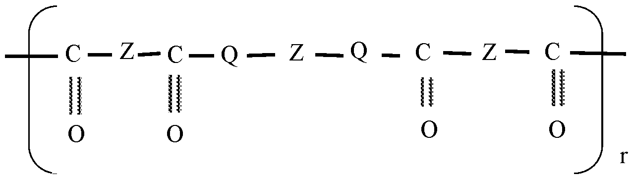
Formula III
9. The electrophoretic medium of claim 7 or claim 8, wherein the molecular structure of the charge control agent is represented by Formula IV, wherein
Rl, R2, and R3 are independently selected by the group consisting of an alkyl, aryl, and alkenyl group, each Q is independently selected from the group consisting of O and NH group, each -Z- is independently selected from the group consisting of an aliphatic biradical unit -A- and an aliphatic biradical unit -B-, -A- being represented by Formula I, and -B- being represented by Formula II, and r is an integer from 1 to 20.

Rl, R2, and R3 are independently selected by the group consisting of alkyl, aryl, and alkenyl group, each Q is independently selected from the group consisting of oxygen and NH group, each G is independently selected from the group consisting of oxygen, sulfur, and NH group,
D is -(CH2)t -, where t is an integer from 3 to 6, each -Z- is independently selected from the group consisting of an aliphatic biradical unit -A- and an aliphatic biradical unit -B-, -A- being represented by Formula I, and -B- being represented by Formula II, and r is an integer from 1 to 20.

11. The electrophoretic medium of claim 7 or claim 8, wherein the molecular structure of the charge control agent is represented by Formula VI, wherein
Rl, R2, and R3 are independently selected by the group consisting of alkyl, aryl, and alkenyl group, each Q is independently selected from the group consisting of oxygen and NH group,
each -Z- is independently selected from the group consisting of an aliphatic biradical unit -A- and an aliphatic biradical unit -B-, -A- being represented by Formula I, and -B- being represented by Formula II, and r is an integer from 1 to 20.
 Formula VI,
12. The electrophoretic medium of claim 10, wherein the molecular structure of the charge control agent is represented by Formula V, wherein Rl, R2, R3 are methyl, G is oxygen or NH, Q is oxygen, D is -(CH2)3-, and -Z- is an aliphatic biradical unit that is represented by Formula I.
13. The electrophoretic medium according to any one of claim 1 to claim 12 comprising a plurality of first, second, and third types of charged pigment particles, wherein each type of charged pigment particles has different color from each other type of charged pigment particles.
14. The electrophoretic medium according to any one of claim 1 to claim 13, wherein the charge control agent has a weight average molecular weight greater than or equal to 1000 g/mol.
15. The electrophoretic medium according to any one of claim 1 to claim 14, wherein the charge control agent has a weight average molecular weight from 1000 g/mol to 8,000 g/mol.
16. The electrophoretic medium according to any one of claim 1 to claim 15, further comprising a second charge control agent, wherein the second charge control agent comprises a hydrophobic moiety and a head group selected from the group comprising an anionic functional group, a nonionic functional group, and a cationic functional group.
17. The electrophoretic medium according to any one of claim 1 to claim 16, wherein the plurality of charged pigment particles are capable of moving through the non-polar liquid upon application of an electric field.
18. An electro-optic display comprising a light transmissive, electrically-conductive layer, an electro-optic material layer, and a substrate comprising a plurality of pixel electrodes, wherein the electro-optic material layer comprises the electrophoretic medium according to any one of claim 1 to claim 17.
19. The electro-optic display of claim 18, wherein the electrophoretic medium is encapsulated in a plurality of microcapsules or in a plurality of microcells.
20. The electro-optic display of claim 19, wherein each of the plurality of microcells includes a bottom layer, partition walls, an opening, and a sealing layer, the sealing layer spanning the opening of each microcell.
Applications Claiming Priority (2)
| Application Number | Priority Date | Filing Date | Title |
|---|---|---|---|
| US202463616957P | 2024-01-02 | 2024-01-02 | |
| US63/616,957 | 2024-01-02 |
Publications (2)
| Publication Number | Publication Date |
|---|---|
| WO2025147410A2 true WO2025147410A2 (en) | 2025-07-10 |
| WO2025147410A3 WO2025147410A3 (en) | 2025-08-07 |
Family
ID=94341348
Family Applications (1)
| Application Number | Title | Priority Date | Filing Date |
|---|---|---|---|
| PCT/US2024/061641 Pending WO2025147410A2 (en) | 2024-01-02 | 2024-12-23 | Electrophoretic media comprising a cationic charge control agent |
Country Status (3)
| Country | Link |
|---|---|
| US (1) | US20250216737A1 (en) |
| TW (1) | TW202540273A (en) |
| WO (1) | WO2025147410A2 (en) |
Citations (464)
| Publication number | Priority date | Publication date | Assignee | Title |
|---|---|---|---|---|
| US4418346A (en) | 1981-05-20 | 1983-11-29 | Batchelder J Samuel | Method and apparatus for providing a dielectrophoretic display of visual information |
| US5872552A (en) | 1994-12-28 | 1999-02-16 | International Business Machines Corporation | Electrophoretic display |
| US5930026A (en) | 1996-10-25 | 1999-07-27 | Massachusetts Institute Of Technology | Nonemissive displays and piezoelectric power supplies therefor |
| US5961804A (en) | 1997-03-18 | 1999-10-05 | Massachusetts Institute Of Technology | Microencapsulated electrophoretic display |
| WO1999067678A2 (en) | 1998-06-22 | 1999-12-29 | E-Ink Corporation | Means of addressing microencapsulated display media |
| US6017584A (en) | 1995-07-20 | 2000-01-25 | E Ink Corporation | Multi-color electrophoretic displays and materials for making the same |
| WO2000005704A1 (en) | 1998-07-22 | 2000-02-03 | E-Ink Corporation | Electronic display |
| US6067185A (en) | 1997-08-28 | 2000-05-23 | E Ink Corporation | Process for creating an encapsulated electrophoretic display |
| WO2000036560A1 (en) | 1998-12-18 | 2000-06-22 | E Ink Corporation | Electronic ink display media for security and authentication |
| WO2000038000A1 (en) | 1998-12-22 | 2000-06-29 | E Ink Corporation | Method of manufacturing of a discrete electronic device |
| US6118426A (en) | 1995-07-20 | 2000-09-12 | E Ink Corporation | Transducers and indicators having printed displays |
| US6120588A (en) | 1996-07-19 | 2000-09-19 | E Ink Corporation | Electronically addressable microencapsulated ink and display thereof |
| US6120839A (en) | 1995-07-20 | 2000-09-19 | E Ink Corporation | Electro-osmotic displays and materials for making the same |
| US6124851A (en) | 1995-07-20 | 2000-09-26 | E Ink Corporation | Electronic book with multiple page displays |
| US6130774A (en) | 1998-04-27 | 2000-10-10 | E Ink Corporation | Shutter mode microencapsulated electrophoretic display |
| US6144361A (en) | 1998-09-16 | 2000-11-07 | International Business Machines Corporation | Transmissive electrophoretic display with vertical electrodes |
| US6177921B1 (en) | 1997-08-28 | 2001-01-23 | E Ink Corporation | Printable electrode structures for displays |
| US6184856B1 (en) | 1998-09-16 | 2001-02-06 | International Business Machines Corporation | Transmissive electrophoretic display with laterally adjacent color cells |
| US6225971B1 (en) | 1998-09-16 | 2001-05-01 | International Business Machines Corporation | Reflective electrophoretic display with laterally adjacent color cells using an absorbing panel |
| US6232950B1 (en) | 1997-08-28 | 2001-05-15 | E Ink Corporation | Rear electrode structures for displays |
| US6241921B1 (en) | 1998-05-15 | 2001-06-05 | Massachusetts Institute Of Technology | Heterogeneous display elements and methods for their fabrication |
| US6252564B1 (en) | 1997-08-28 | 2001-06-26 | E Ink Corporation | Tiled displays |
| US6262833B1 (en) | 1998-10-07 | 2001-07-17 | E Ink Corporation | Capsules for electrophoretic displays and methods for making the same |
| US6262706B1 (en) | 1995-07-20 | 2001-07-17 | E Ink Corporation | Retroreflective electrophoretic displays and materials for making the same |
| US6271823B1 (en) | 1998-09-16 | 2001-08-07 | International Business Machines Corporation | Reflective electrophoretic display with laterally adjacent color cells using a reflective panel |
| US6300932B1 (en) | 1997-08-28 | 2001-10-09 | E Ink Corporation | Electrophoretic displays with luminescent particles and materials for making the same |
| US6312971B1 (en) | 1999-08-31 | 2001-11-06 | E Ink Corporation | Solvent annealing process for forming a thin semiconductor film with advantageous properties |
| US6312304B1 (en) | 1998-12-15 | 2001-11-06 | E Ink Corporation | Assembly of microencapsulated electronic displays |
| US6323989B1 (en) | 1996-07-19 | 2001-11-27 | E Ink Corporation | Electrophoretic displays using nanoparticles |
| US6327072B1 (en) | 1999-04-06 | 2001-12-04 | E Ink Corporation | Microcell electrophoretic displays |
| US6376828B1 (en) | 1998-10-07 | 2002-04-23 | E Ink Corporation | Illumination system for nonemissive electronic displays |
| US6377387B1 (en) | 1999-04-06 | 2002-04-23 | E Ink Corporation | Methods for producing droplets for use in capsule-based electrophoretic displays |
| US6392786B1 (en) | 1999-07-01 | 2002-05-21 | E Ink Corporation | Electrophoretic medium provided with spacers |
| US20020060321A1 (en) | 2000-07-14 | 2002-05-23 | Kazlas Peter T. | Minimally- patterned, thin-film semiconductor devices for display applications |
| US6413790B1 (en) | 1999-07-21 | 2002-07-02 | E Ink Corporation | Preferred methods for producing electrical circuit elements used to control an electronic display |
| US20020090980A1 (en) | 2000-12-05 | 2002-07-11 | Wilcox Russell J. | Displays for portable electronic apparatus |
| US6445489B1 (en) | 1998-03-18 | 2002-09-03 | E Ink Corporation | Electrophoretic displays and systems for addressing such displays |
| US6459418B1 (en) | 1995-07-20 | 2002-10-01 | E Ink Corporation | Displays combining active and non-active inks |
| US6473072B1 (en) | 1998-05-12 | 2002-10-29 | E Ink Corporation | Microencapsulated electrophoretic electrostatically-addressed media for drawing device applications |
| US6480182B2 (en) | 1997-03-18 | 2002-11-12 | Massachusetts Institute Of Technology | Printable electronic display |
| US20020188053A1 (en) | 2001-06-04 | 2002-12-12 | Sipix Imaging, Inc. | Composition and process for the sealing of microcups in roll-to-roll display manufacturing |
| US6498114B1 (en) | 1999-04-09 | 2002-12-24 | E Ink Corporation | Method for forming a patterned semiconductor film |
| US6504524B1 (en) | 2000-03-08 | 2003-01-07 | E Ink Corporation | Addressing methods for displays having zero time-average field |
| US6506438B2 (en) | 1998-12-15 | 2003-01-14 | E Ink Corporation | Method for printing of transistor arrays on plastic substrates |
| US6512354B2 (en) | 1998-07-08 | 2003-01-28 | E Ink Corporation | Method and apparatus for sensing the state of an electrophoretic display |
| US6515649B1 (en) | 1995-07-20 | 2003-02-04 | E Ink Corporation | Suspended particle displays and materials for making the same |
| US6518949B2 (en) | 1998-04-10 | 2003-02-11 | E Ink Corporation | Electronic displays using organic-based field effect transistors |
| US6531997B1 (en) | 1999-04-30 | 2003-03-11 | E Ink Corporation | Methods for addressing electrophoretic displays |
| US20030048522A1 (en) | 2001-09-13 | 2003-03-13 | Rong-Chang Liang | Three-dimensional electrophoretic displays |
| US6538801B2 (en) | 1996-07-19 | 2003-03-25 | E Ink Corporation | Electrophoretic displays using nanoparticles |
| US6545797B2 (en) | 2001-06-11 | 2003-04-08 | Sipix Imaging, Inc. | Process for imagewise opening and filling color display components and color displays manufactured thereof |
| US6545291B1 (en) | 1999-08-31 | 2003-04-08 | E Ink Corporation | Transistor design for use in the construction of an electronically driven display |
| US20030102858A1 (en) | 1998-07-08 | 2003-06-05 | E Ink Corporation | Method and apparatus for determining properties of an electrophoretic display |
| US6580545B2 (en) | 2001-04-19 | 2003-06-17 | E Ink Corporation | Electrochromic-nanoparticle displays |
| US20030151029A1 (en) | 2002-02-11 | 2003-08-14 | Hsu Wan Peter | Core-shell particles for electrophoretic display |
| US20030164480A1 (en) | 2002-01-03 | 2003-09-04 | Wu Zarng-Arh George | Novel electrophoretic dispersion with a fluorinated solvent and a charge controlling agent |
| US6639578B1 (en) | 1995-07-20 | 2003-10-28 | E Ink Corporation | Flexible displays |
| US20030203101A1 (en) | 2002-04-24 | 2003-10-30 | Sipix Imaging, Inc. | Process for forming a patterned thin film conductive structure on a substrate |
| US6657772B2 (en) | 2001-07-09 | 2003-12-02 | E Ink Corporation | Electro-optic display and adhesive composition for use therein |
| US6664944B1 (en) | 1995-07-20 | 2003-12-16 | E-Ink Corporation | Rear electrode structures for electrophoretic displays |
| US6672921B1 (en) | 2000-03-03 | 2004-01-06 | Sipix Imaging, Inc. | Manufacturing process for electrophoretic display |
| USD485294S1 (en) | 1998-07-22 | 2004-01-13 | E Ink Corporation | Electrode structure for an electronic display |
| US20040030125A1 (en) | 2002-05-17 | 2004-02-12 | Ying-Syi Li | Novel Fluorinated silicon (IV) phthalocyanines and naphthalocyanines for electrophoretic, magnetophoretic or electromagnetophoretic display |
| US6693620B1 (en) | 1999-05-03 | 2004-02-17 | E Ink Corporation | Threshold addressing of electrophoretic displays |
| US6704133B2 (en) | 1998-03-18 | 2004-03-09 | E-Ink Corporation | Electro-optic display overlays and systems for addressing such displays |
| US6710540B1 (en) | 1995-07-20 | 2004-03-23 | E Ink Corporation | Electrostatically-addressable electrophoretic display |
| US6721083B2 (en) | 1996-07-19 | 2004-04-13 | E Ink Corporation | Electrophoretic displays using nanoparticles |
| US6727881B1 (en) | 1995-07-20 | 2004-04-27 | E Ink Corporation | Encapsulated electrophoretic displays and methods and materials for making the same |
| US20040085619A1 (en) | 2002-07-17 | 2004-05-06 | Wu Zarng-Arh George | Novel Methods and compositions for improved electrophoretic display performance |
| US20040105036A1 (en) | 2002-08-06 | 2004-06-03 | E Ink Corporation | Protection of electro-optic displays against thermal effects |
| US6751007B2 (en) | 2001-08-20 | 2004-06-15 | Sipix Imaging, Inc. | Transflective electrophoretic display |
| US6753999B2 (en) | 1998-03-18 | 2004-06-22 | E Ink Corporation | Electrophoretic displays in portable devices and systems for addressing such displays |
| US6753067B2 (en) | 2001-04-23 | 2004-06-22 | Sipix Imaging, Inc. | Microcup compositions having improved flexure resistance and release properties |
| US20040119681A1 (en) | 1998-11-02 | 2004-06-24 | E Ink Corporation | Broadcast system for electronic ink signs |
| US20040120024A1 (en) | 2002-09-23 | 2004-06-24 | Chen Huiyong Paul | Electrophoretic displays with improved high temperature performance |
| US6781745B2 (en) | 2001-09-12 | 2004-08-24 | Sipix Imaging, Inc. | Electrophoretic display with gating electrodes |
| US6784953B2 (en) | 2001-01-11 | 2004-08-31 | Sipix Imaging, Inc. | Transmissive or reflective liquid crystal display and novel process for its manufacture |
| US6788452B2 (en) | 2001-06-11 | 2004-09-07 | Sipix Imaging, Inc. | Process for manufacture of improved color displays |
| US6788449B2 (en) | 2000-03-03 | 2004-09-07 | Sipix Imaging, Inc. | Electrophoretic display and novel process for its manufacture |
| US6795229B2 (en) | 2001-08-28 | 2004-09-21 | Sipix Imaging, Inc. | Electrophoretic display with sub relief structure for high contrast ratio and improved shear and/or compression resistance |
| US6806995B2 (en) | 2001-10-29 | 2004-10-19 | Sipix Imaging, Inc. | Electrophoretic display with holding electrodes |
| US20040219306A1 (en) | 2003-01-24 | 2004-11-04 | Xiaojia Wang | Adhesive and sealing layers for electrophoretic displays |
| US6822782B2 (en) | 2001-05-15 | 2004-11-23 | E Ink Corporation | Electrophoretic particles and processes for the production thereof |
| US6825829B1 (en) | 1997-08-28 | 2004-11-30 | E Ink Corporation | Adhesive backed displays |
| US6825970B2 (en) | 2001-09-14 | 2004-11-30 | E Ink Corporation | Methods for addressing electro-optic materials |
| US6829078B2 (en) | 2000-03-03 | 2004-12-07 | Sipix Imaging Inc. | Electrophoretic display and novel process for its manufacture |
| US20040246562A1 (en) | 2003-05-16 | 2004-12-09 | Sipix Imaging, Inc. | Passive matrix electrophoretic display driving scheme |
| US6831771B2 (en) | 2003-01-08 | 2004-12-14 | Sipix Imaging Inc. | Electronic whiteboard using electrophoretic display |
| US6831770B2 (en) | 2000-03-03 | 2004-12-14 | Sipix Imaging, Inc. | Electrophoretic display and novel process for its manufacture |
| US6833943B2 (en) | 2000-03-03 | 2004-12-21 | Sipix Imaging, Inc. | Electrophoretic display and novel process for its manufacture |
| US6839158B2 (en) | 1997-08-28 | 2005-01-04 | E Ink Corporation | Encapsulated electrophoretic displays having a monolayer of capsules and materials and methods for making the same |
| US20050012980A1 (en) | 2003-05-02 | 2005-01-20 | E Ink Corporation | Electrophoretic displays with controlled amounts of pigment |
| US6850355B2 (en) | 2001-07-27 | 2005-02-01 | Sipix Imaging, Inc. | Electrophoretic display with color filters |
| US6864875B2 (en) | 1998-04-10 | 2005-03-08 | E Ink Corporation | Full color reflective display with multichromatic sub-pixels |
| US6865012B2 (en) | 2000-03-03 | 2005-03-08 | Sipix Imaging, Inc. | Electrophoretic display and novel process for its manufacture |
| US6866760B2 (en) | 1998-08-27 | 2005-03-15 | E Ink Corporation | Electrophoretic medium and process for the production thereof |
| US6870661B2 (en) | 2001-05-15 | 2005-03-22 | E Ink Corporation | Electrophoretic displays containing magnetic particles |
| US6870662B2 (en) | 2002-05-03 | 2005-03-22 | Sipix Imaging, Inc. | Methods of surface modification for improving electrophoretic display performance |
| US6885495B2 (en) | 2000-03-03 | 2005-04-26 | Sipix Imaging Inc. | Electrophoretic display with in-plane switching |
| US20050099575A1 (en) | 2001-01-11 | 2005-05-12 | Rong-Chang Liang | Transmissive or reflective liquid crystal display and process for its manufacture |
| US6900851B2 (en) | 2002-02-08 | 2005-05-31 | E Ink Corporation | Electro-optic displays and optical systems for addressing such displays |
| US20050122306A1 (en) | 2003-10-29 | 2005-06-09 | E Ink Corporation | Electro-optic displays with single edge addressing and removable driver circuitry |
| US20050122563A1 (en) | 2003-07-24 | 2005-06-09 | E Ink Corporation | Electro-optic displays |
| US6914714B2 (en) | 2001-06-11 | 2005-07-05 | Sipix Imaging Inc. | Process for imagewise opening and filling color display components and color displays manufactured thereof |
| US6914713B2 (en) | 2002-04-23 | 2005-07-05 | Sipix Imaging, Inc. | Electro-magnetophoresis display |
| US20050156340A1 (en) | 2004-01-20 | 2005-07-21 | E Ink Corporation | Preparation of capsules |
| US6922276B2 (en) | 2002-12-23 | 2005-07-26 | E Ink Corporation | Flexible electro-optic displays |
| US6927892B2 (en) | 2002-03-21 | 2005-08-09 | Sipix Imaging Inc. | Magnetophoretic and electromagnetophoretic displays |
| US6930818B1 (en) | 2000-03-03 | 2005-08-16 | Sipix Imaging, Inc. | Electrophoretic display and novel process for its manufacture |
| US6933098B2 (en) | 2000-01-11 | 2005-08-23 | Sipix Imaging Inc. | Process for roll-to-roll manufacture of a display by synchronized photolithographic exposure on a substrate web |
| US6947202B2 (en) | 2000-03-03 | 2005-09-20 | Sipix Imaging, Inc. | Electrophoretic display with sub relief structure for high contrast ratio and improved shear and/or compression resistance |
| US6950220B2 (en) | 2002-03-18 | 2005-09-27 | E Ink Corporation | Electro-optic displays, and methods for driving same |
| US6956690B2 (en) | 2003-02-06 | 2005-10-18 | Sipix Imaging, Inc. | Electrophoretic display with a bi-modal particle system |
| US6958848B2 (en) | 2002-05-23 | 2005-10-25 | E Ink Corporation | Capsules, materials for use therein and electrophoretic media and displays containing such capsules |
| US6958849B2 (en) | 2002-09-18 | 2005-10-25 | Sipix Imaging Inc. | Electrophoretic display with improved temperature latitude and switching performance |
| US20050253777A1 (en) | 2004-05-12 | 2005-11-17 | E Ink Corporation | Tiled displays and methods for driving same |
| US6982178B2 (en) | 2002-06-10 | 2006-01-03 | E Ink Corporation | Components and methods for use in electro-optic displays |
| US6987603B2 (en) | 2003-01-31 | 2006-01-17 | E Ink Corporation | Construction of electrophoretic displays |
| US7002728B2 (en) | 1997-08-28 | 2006-02-21 | E Ink Corporation | Electrophoretic particles, and processes for the production thereof |
| US7012600B2 (en) | 1999-04-30 | 2006-03-14 | E Ink Corporation | Methods for driving bistable electro-optic displays, and apparatus for use therein |
| US7023420B2 (en) | 2000-11-29 | 2006-04-04 | E Ink Corporation | Electronic display with photo-addressing means |
| US7030854B2 (en) | 2001-03-13 | 2006-04-18 | E Ink Corporation | Apparatus for displaying drawings |
| US7034783B2 (en) | 2003-08-19 | 2006-04-25 | E Ink Corporation | Method for controlling electro-optic display |
| US7038670B2 (en) | 2002-08-16 | 2006-05-02 | Sipix Imaging, Inc. | Electrophoretic display with dual mode switching |
| US7038655B2 (en) | 1999-05-03 | 2006-05-02 | E Ink Corporation | Electrophoretic ink composed of particles with field dependent mobilities |
| US7038656B2 (en) | 2002-08-16 | 2006-05-02 | Sipix Imaging, Inc. | Electrophoretic display with dual-mode switching |
| US7046228B2 (en) | 2001-08-17 | 2006-05-16 | Sipix Imaging, Inc. | Electrophoretic display with dual mode switching |
| US7052571B2 (en) | 2000-03-03 | 2006-05-30 | Sipix Imaging, Inc. | Electrophoretic display and process for its manufacture |
| US7052766B2 (en) | 2002-01-03 | 2006-05-30 | Sipix Imaging, Inc. | Functionalized halogenated polymers for microencapsulation |
| US7061166B2 (en) | 2003-05-27 | 2006-06-13 | Fuji Photo Film Co., Ltd. | Laminated structure and method of manufacturing the same |
| US7061662B2 (en) | 2003-10-07 | 2006-06-13 | Sipix Imaging, Inc. | Electrophoretic display with thermal control |
| US7072095B2 (en) | 2002-10-31 | 2006-07-04 | Sipix Imaging, Inc. | Electrophoretic display and novel process for its manufacture |
| US7079303B2 (en) | 2002-04-23 | 2006-07-18 | Sipix Imaging, Inc. | Segment electrophoretic displays and methods for their manufacture |
| US7110164B2 (en) | 2002-06-10 | 2006-09-19 | E Ink Corporation | Electro-optic displays, and processes for the production thereof |
| US7113323B2 (en) | 2002-03-21 | 2006-09-26 | Sipix Imaging, Inc. | Magnetophoretic and electromagnetophoretic displays |
| US7116466B2 (en) | 2004-07-27 | 2006-10-03 | E Ink Corporation | Electro-optic displays |
| US7119759B2 (en) | 1999-05-03 | 2006-10-10 | E Ink Corporation | Machine-readable displays |
| US7119772B2 (en) | 1999-04-30 | 2006-10-10 | E Ink Corporation | Methods for driving bistable electro-optic displays, and apparatus for use therein |
| US20060255322A1 (en) | 2002-07-17 | 2006-11-16 | Wu Zarng-Arh G | Methods and compositions for improved electrophoretic display performance |
| US20060262249A1 (en) | 2001-01-11 | 2006-11-23 | Rong-Chang Liang | Transmissive or reflective liquid crystal display and process for its manufacture |
| US7141688B2 (en) | 2002-10-15 | 2006-11-28 | Sipix Imaging, Inc. | Fluorinated dye stabilizers in fluorinated dielectric solvent |
| US7142351B2 (en) | 2000-03-03 | 2006-11-28 | Sipix Imaging, Inc. | Electro-magnetophoresis display |
| US7141279B2 (en) | 2002-11-25 | 2006-11-28 | Sipix Imaging, Inc. | Transmissive or reflective liquid crystal display and novel process for its manufacture |
| US7156945B2 (en) | 2002-04-24 | 2007-01-02 | Sipix Imaging, Inc. | Process for forming a patterned thin film structure for in-mold decoration |
| US7158282B2 (en) | 2000-03-03 | 2007-01-02 | Sipix Imaging, Inc. | Electrophoretic display and novel process for its manufacture |
| US7167155B1 (en) | 1995-07-20 | 2007-01-23 | E Ink Corporation | Color electrophoretic displays |
| US7166182B2 (en) | 2002-09-04 | 2007-01-23 | Sipix Imaging, Inc. | Adhesive and sealing layers for electrophoretic displays |
| US7170670B2 (en) | 2001-04-02 | 2007-01-30 | E Ink Corporation | Electrophoretic medium and display with improved image stability |
| US7177066B2 (en) | 2003-10-24 | 2007-02-13 | Sipix Imaging, Inc. | Electrophoretic display driving scheme |
| US20070042135A1 (en) | 2002-11-25 | 2007-02-22 | Rong-Chang Liang | Transmissive or reflective liquid crystal display |
| US7182830B2 (en) | 2003-02-04 | 2007-02-27 | Sipix Imaging, Inc. | Compositions and assembly process for liquid crystal display |
| US7184197B2 (en) | 2003-01-30 | 2007-02-27 | Sipix Imaging, Inc. | High performance capsules for electrophoretic displays |
| US7193625B2 (en) | 1999-04-30 | 2007-03-20 | E Ink Corporation | Methods for driving electro-optic displays, and apparatus for use therein |
| US7202847B2 (en) | 2002-06-28 | 2007-04-10 | E Ink Corporation | Voltage modulated driver circuits for electro-optic displays |
| US7205355B2 (en) | 2001-06-04 | 2007-04-17 | Sipix Imaging, Inc. | Composition and process for the manufacture of an improved electrophoretic display |
| US20070091417A1 (en) | 2005-10-25 | 2007-04-26 | E Ink Corporation | Electrophoretic media and displays with improved binder |
| US20070103427A1 (en) | 2003-11-25 | 2007-05-10 | Koninklijke Philips Electronice N.V. | Display apparatus with a display device and a cyclic rail-stabilized method of driving the display device |
| US7226550B2 (en) | 2002-10-10 | 2007-06-05 | Sipix Imaging, Inc. | Electrophoretic dispersions |
| US7230750B2 (en) | 2001-05-15 | 2007-06-12 | E Ink Corporation | Electrophoretic media and processes for the production thereof |
| US7230751B2 (en) | 2005-01-26 | 2007-06-12 | E Ink Corporation | Electrophoretic displays using gaseous fluids |
| US7233429B2 (en) | 2000-03-03 | 2007-06-19 | Sipix Imaging, Inc. | Electrophoretic display |
| US7236290B1 (en) | 2000-07-25 | 2007-06-26 | E Ink Corporation | Electrophoretic medium with improved stability |
| US20070153360A1 (en) | 2002-03-21 | 2007-07-05 | Ching-Shon Ho | Magnetophoretic and electromagnetophoretic displays |
| US7245414B2 (en) | 2002-09-10 | 2007-07-17 | Sipix Imaging, Inc. | Electrochromic or electrodeposition display and novel process for their manufacture |
| US20070176912A1 (en) | 2005-12-09 | 2007-08-02 | Beames Michael H | Portable memory devices with polymeric displays |
| US7259744B2 (en) | 1995-07-20 | 2007-08-21 | E Ink Corporation | Dielectrophoretic displays |
| US7261920B2 (en) | 2002-04-24 | 2007-08-28 | Sipix Imaging, Inc. | Process for forming a patterned thin film structure on a substrate |
| US7271947B2 (en) | 2002-08-16 | 2007-09-18 | Sipix Imaging, Inc. | Electrophoretic display with dual-mode switching |
| US7277218B2 (en) | 2003-11-04 | 2007-10-02 | Sipix Imaging, Inc. | Electrophoretic compositions |
| US20070237962A1 (en) | 2000-03-03 | 2007-10-11 | Rong-Chang Liang | Semi-finished display panels |
| US7286279B2 (en) | 2002-07-30 | 2007-10-23 | Sipix Imaging, Inc. | Microencapsulation processes and compositions for electrophoretic displays |
| US7304780B2 (en) | 2004-12-17 | 2007-12-04 | Sipix Imaging, Inc. | Backplane design for display panels and processes for their manufacture |
| US7304634B2 (en) | 1995-07-20 | 2007-12-04 | E Ink Corporation | Rear electrode structures for electrophoretic displays |
| US7307778B2 (en) | 2002-04-24 | 2007-12-11 | Sipix Imaging, Inc. | Compositions and processes for format-flexible, roll-to-roll manufacturing of electrophoretic displays |
| US20070285385A1 (en) | 1998-11-02 | 2007-12-13 | E Ink Corporation | Broadcast system for electronic ink signs |
| US7312916B2 (en) | 2002-08-07 | 2007-12-25 | E Ink Corporation | Electrophoretic media containing specularly reflective particles |
| US20080020007A1 (en) | 2006-07-18 | 2008-01-24 | Zang Hongmei | Liquid-containing film structure |
| US20080024482A1 (en) | 2002-06-13 | 2008-01-31 | E Ink Corporation | Methods for driving electro-optic displays |
| US20080024429A1 (en) | 2006-07-25 | 2008-01-31 | E Ink Corporation | Electrophoretic displays using gaseous fluids |
| US7327346B2 (en) | 2002-05-29 | 2008-02-05 | Sipix Imaging, Inc. | Electrode and connecting designs for roll-to-roll format flexible display manufacturing |
| US7327511B2 (en) | 2004-03-23 | 2008-02-05 | E Ink Corporation | Light modulators |
| US20080043318A1 (en) | 2005-10-18 | 2008-02-21 | E Ink Corporation | Color electro-optic displays, and processes for the production thereof |
| US7339715B2 (en) | 2003-03-25 | 2008-03-04 | E Ink Corporation | Processes for the production of electrophoretic displays |
| US7347957B2 (en) | 2003-07-10 | 2008-03-25 | Sipix Imaging, Inc. | Methods and compositions for improved electrophoretic display performance |
| US7374634B2 (en) | 2004-05-12 | 2008-05-20 | Sipix Imaging, Inc. | Process for the manufacture of electrophoretic displays |
| US7382514B2 (en) | 2002-02-11 | 2008-06-03 | Sipix Imaging, Inc. | Core-shell particles for electrophoretic display |
| US7385751B2 (en) | 2001-06-11 | 2008-06-10 | Sipix Imaging, Inc. | Process for imagewise opening and filling color display components and color displays manufactured thereof |
| US20080136774A1 (en) | 2004-07-27 | 2008-06-12 | E Ink Corporation | Methods for driving electrophoretic displays using dielectrophoretic forces |
| US7390901B2 (en) | 2003-08-08 | 2008-06-24 | Sipix Imaging, Inc. | Fluorinated dyes or colorants and their uses |
| US7408699B2 (en) | 2005-09-28 | 2008-08-05 | Sipix Imaging, Inc. | Electrophoretic display and methods of addressing such display |
| US7408696B2 (en) | 2000-03-03 | 2008-08-05 | Sipix Imaging, Inc. | Three-dimensional electrophoretic displays |
| US7411719B2 (en) | 1995-07-20 | 2008-08-12 | E Ink Corporation | Electrophoretic medium and process for the production thereof |
| US7420549B2 (en) | 2003-10-08 | 2008-09-02 | E Ink Corporation | Electro-wetting displays |
| US7453445B2 (en) | 2004-08-13 | 2008-11-18 | E Ink Corproation | Methods for driving electro-optic displays |
| US20080291129A1 (en) | 2007-05-21 | 2008-11-27 | E Ink Corporation | Methods for driving video electro-optic displays |
| US20080303780A1 (en) | 2007-06-07 | 2008-12-11 | Sipix Imaging, Inc. | Driving methods and circuit for bi-stable displays |
| US7470386B2 (en) | 2004-04-26 | 2008-12-30 | Sipix Imaging, Inc. | Roll-to-roll embossing tools and processes |
| US20090009852A1 (en) | 2001-05-15 | 2009-01-08 | E Ink Corporation | Electrophoretic particles and processes for the production thereof |
| US7477444B2 (en) | 2006-09-22 | 2009-01-13 | E Ink Corporation & Air Products And Chemical, Inc. | Electro-optic display and materials for use therein |
| US7492505B2 (en) | 2001-08-17 | 2009-02-17 | Sipix Imaging, Inc. | Electrophoretic display with dual mode switching |
| US7492339B2 (en) | 2004-03-26 | 2009-02-17 | E Ink Corporation | Methods for driving bistable electro-optic displays |
| US7504050B2 (en) | 2004-02-23 | 2009-03-17 | Sipix Imaging, Inc. | Modification of electrical properties of display cells for improving electrophoretic display performance |
| US7528822B2 (en) | 2001-11-20 | 2009-05-05 | E Ink Corporation | Methods for driving electro-optic displays |
| US20090122389A1 (en) | 2007-11-14 | 2009-05-14 | E Ink Corporation | Electro-optic assemblies, and adhesives and binders for use therein |
| US7554712B2 (en) | 2005-06-23 | 2009-06-30 | E Ink Corporation | Edge seals for, and processes for assembly of, electro-optic displays |
| US7557981B2 (en) | 2000-03-03 | 2009-07-07 | Sipix Imaging, Inc. | Electrophoretic display and process for its manufacture |
| US20090174651A1 (en) | 1995-07-20 | 2009-07-09 | E Ink Corporation | Addressing schemes for electronic displays |
| US7561324B2 (en) | 2002-09-03 | 2009-07-14 | E Ink Corporation | Electro-optic displays |
| US7560004B2 (en) | 2002-09-04 | 2009-07-14 | Sipix Imaging, Inc. | Adhesive and sealing layers for electrophoretic displays |
| US7564614B2 (en) | 2004-05-20 | 2009-07-21 | Sipix Imaging, Inc. | Electrode protection film for electrophoretic displays |
| US20090195568A1 (en) | 2003-03-31 | 2009-08-06 | E Ink Corporation | Methods for driving electro-optic displays |
| US7572491B2 (en) | 2003-01-24 | 2009-08-11 | Sipix Imaging, Inc. | Adhesive and sealing layers for electrophoretic displays |
| US7572394B2 (en) | 2003-11-04 | 2009-08-11 | Sipix Imaging, Inc. | Electrophoretic dispersions |
| US7576904B2 (en) | 2000-03-03 | 2009-08-18 | Sipix Imaging, Inc. | Electro-magnetophoresis display |
| US7583251B2 (en) | 1995-07-20 | 2009-09-01 | E Ink Corporation | Dielectrophoretic displays |
| US7602374B2 (en) | 2003-09-19 | 2009-10-13 | E Ink Corporation | Methods for reducing edge effects in electro-optic displays |
| US7612760B2 (en) | 2005-02-17 | 2009-11-03 | Seiko Epson Corporation | Electrophoresis device, method of driving electrophoresis device, and electronic apparatus |
| US7616374B2 (en) | 2002-09-23 | 2009-11-10 | Sipix Imaging, Inc. | Electrophoretic displays with improved high temperature performance |
| US7649666B2 (en) | 2006-12-07 | 2010-01-19 | E Ink Corporation | Components and methods for use in electro-optic displays |
| US7667684B2 (en) | 1998-07-08 | 2010-02-23 | E Ink Corporation | Methods for achieving improved color in microencapsulated electrophoretic devices |
| US7679814B2 (en) | 2001-04-02 | 2010-03-16 | E Ink Corporation | Materials for use in electrophoretic displays |
| US7679599B2 (en) | 2005-03-04 | 2010-03-16 | Seiko Epson Corporation | Electrophoretic device, method of driving electrophoretic device, and electronic apparatus |
| US7683606B2 (en) | 2006-05-26 | 2010-03-23 | Sipix Imaging, Inc. | Flexible display testing and inspection |
| US7715088B2 (en) | 2000-03-03 | 2010-05-11 | Sipix Imaging, Inc. | Electrophoretic display |
| US7715087B2 (en) | 2000-03-03 | 2010-05-11 | Sipix Imaging, Inc. | Segment electrophoretic displays and methods for their manufacture |
| US20100177396A1 (en) | 2009-01-13 | 2010-07-15 | Craig Lin | Asymmetrical luminance enhancement structure for reflective display devices |
| US7767126B2 (en) | 2005-08-22 | 2010-08-03 | Sipix Imaging, Inc. | Embossing assembly and methods of preparation |
| US20100194789A1 (en) | 2009-01-30 | 2010-08-05 | Craig Lin | Partial image update for electrophoretic displays |
| US20100194733A1 (en) | 2009-01-30 | 2010-08-05 | Craig Lin | Multiple voltage level driving for electrophoretic displays |
| US7791789B2 (en) | 1995-07-20 | 2010-09-07 | E Ink Corporation | Multi-color electrophoretic displays and materials for making the same |
| US7826129B2 (en) | 2007-03-06 | 2010-11-02 | E Ink Corporation | Materials for use in electrophoretic displays |
| US20100283804A1 (en) | 2009-05-11 | 2010-11-11 | Sipix Imaging, Inc. | Driving Methods And Waveforms For Electrophoretic Displays |
| US7839564B2 (en) | 2002-09-03 | 2010-11-23 | E Ink Corporation | Components and methods for use in electro-optic displays |
| US7843624B2 (en) | 2006-03-08 | 2010-11-30 | E Ink Corporation | Electro-optic displays, and materials and methods for production thereof |
| US7843621B2 (en) | 2002-06-10 | 2010-11-30 | E Ink Corporation | Components and testing methods for use in the production of electro-optic displays |
| US7848006B2 (en) | 1995-07-20 | 2010-12-07 | E Ink Corporation | Electrophoretic displays with controlled amounts of pigment |
| US7859742B1 (en) | 2009-12-02 | 2010-12-28 | Sipix Technology, Inc. | Frequency conversion correction circuit for electrophoretic displays |
| US7880958B2 (en) | 2005-09-23 | 2011-02-01 | Sipix Imaging, Inc. | Display cell structure and electrode protecting layer compositions |
| US20110043543A1 (en) | 2009-08-18 | 2011-02-24 | Hui Chen | Color tuning for electrophoretic display |
| US7903319B2 (en) | 2006-07-11 | 2011-03-08 | E Ink Corporation | Electrophoretic medium and display with improved image stability |
| US20110063314A1 (en) | 2009-09-15 | 2011-03-17 | Wen-Pin Chiu | Display controller system |
| US7910175B2 (en) | 2003-03-25 | 2011-03-22 | E Ink Corporation | Processes for the production of electrophoretic displays |
| US7952790B2 (en) | 2006-03-22 | 2011-05-31 | E Ink Corporation | Electro-optic media produced using ink jet printing |
| US7952557B2 (en) | 2001-11-20 | 2011-05-31 | E Ink Corporation | Methods and apparatus for driving electro-optic displays |
| US7956841B2 (en) | 1995-07-20 | 2011-06-07 | E Ink Corporation | Stylus-based addressing structures for displays |
| US20110164301A1 (en) | 2003-11-05 | 2011-07-07 | E Ink Corporation | Electro-optic displays, and materials for use therein |
| US7982479B2 (en) | 2006-04-07 | 2011-07-19 | Sipix Imaging, Inc. | Inspection methods for defects in electrophoretic display and related devices |
| US7982941B2 (en) | 2008-09-02 | 2011-07-19 | Sipix Imaging, Inc. | Color display devices |
| US20110175875A1 (en) | 2010-01-15 | 2011-07-21 | Craig Lin | Driving methods with variable frame time |
| US20110193841A1 (en) | 2002-06-13 | 2011-08-11 | E Ink Corporation | Methods for driving electrophoretic displays using dielectrophoretic forces |
| US20110193840A1 (en) | 1995-07-20 | 2011-08-11 | E Ink Corporation | Methods for driving electrophoretic displays using dielectrophoretic forces |
| US8002948B2 (en) | 2002-04-24 | 2011-08-23 | Sipix Imaging, Inc. | Process for forming a patterned thin film structure on a substrate |
| US8009348B2 (en) | 1999-05-03 | 2011-08-30 | E Ink Corporation | Machine-readable displays |
| US8011592B2 (en) | 2007-01-19 | 2011-09-06 | Sipix Imaging, Inc. | Temperature management in an integrated circuit card with electrophoretic display |
| US20110217639A1 (en) | 2010-03-02 | 2011-09-08 | Sprague Robert A | Electrophoretic display fluid |
| US8018640B2 (en) | 2006-07-13 | 2011-09-13 | E Ink Corporation | Particles for use in electrophoretic displays |
| US20110221740A1 (en) | 2010-03-12 | 2011-09-15 | Sipix Technology Inc. | Driving method of electrophoretic display |
| US8034209B2 (en) | 2007-06-29 | 2011-10-11 | E Ink Corporation | Electro-optic displays, and materials and methods for production thereof |
| US8040594B2 (en) | 1997-08-28 | 2011-10-18 | E Ink Corporation | Multi-color electrophoretic displays |
| US8054526B2 (en) | 2008-03-21 | 2011-11-08 | E Ink Corporation | Electro-optic displays, and color filters for use therein |
| US20110292319A1 (en) | 2010-05-27 | 2011-12-01 | E Ink Corporation | Dual mode electro-optic displays |
| US8077141B2 (en) | 2002-12-16 | 2011-12-13 | E Ink Corporation | Backplanes for electro-optic displays |
| US20120001957A1 (en) | 2010-06-30 | 2012-01-05 | Sipix Technology Inc. | Electrophoretic display and driving method thereof |
| US8098418B2 (en) | 2009-03-03 | 2012-01-17 | E. Ink Corporation | Electro-optic displays, and color filters for use therein |
| US8115729B2 (en) | 1999-05-03 | 2012-02-14 | E Ink Corporation | Electrophoretic display element with filler particles |
| US8125501B2 (en) | 2001-11-20 | 2012-02-28 | E Ink Corporation | Voltage modulated driver circuits for electro-optic displays |
| US20120049125A1 (en) | 2010-08-24 | 2012-03-01 | Hui Du | Electrophoretic dispersion |
| US8129655B2 (en) | 2002-09-03 | 2012-03-06 | E Ink Corporation | Electrophoretic medium with gaseous suspending fluid |
| US8154790B2 (en) | 2008-10-28 | 2012-04-10 | Sipix Imaging, Inc. | Electrophoretic display structures |
| US8159636B2 (en) | 2005-04-08 | 2012-04-17 | Sipix Imaging, Inc. | Reflective displays and processes for their manufacture |
| US20120098740A1 (en) | 2010-10-20 | 2012-04-26 | Sipix Technology Inc. | Electro-phoretic display apparatus |
| US8169690B2 (en) | 2008-02-21 | 2012-05-01 | Sipix Imaging, Inc. | Color display devices |
| US8174490B2 (en) | 2003-06-30 | 2012-05-08 | E Ink Corporation | Methods for driving electrophoretic displays |
| US8177942B2 (en) | 2003-11-05 | 2012-05-15 | E Ink Corporation | Electro-optic displays, and materials for use therein |
| US8213076B2 (en) | 1997-08-28 | 2012-07-03 | E Ink Corporation | Multi-color electrophoretic displays and materials for making the same |
| US8243013B1 (en) | 2007-05-03 | 2012-08-14 | Sipix Imaging, Inc. | Driving bistable displays |
| US8257614B2 (en) | 2003-11-04 | 2012-09-04 | Sipix Imaging, Inc. | Electrophoretic dispersions |
| US8270064B2 (en) | 2009-02-09 | 2012-09-18 | E Ink Corporation | Electrophoretic particles, and processes for the production thereof |
| US8274472B1 (en) | 2007-03-12 | 2012-09-25 | Sipix Imaging, Inc. | Driving methods for bistable displays |
| US8289250B2 (en) | 2004-03-31 | 2012-10-16 | E Ink Corporation | Methods for driving electro-optic displays |
| US8300006B2 (en) | 2003-10-03 | 2012-10-30 | E Ink Corporation | Electrophoretic display unit |
| US8314784B2 (en) | 2008-04-11 | 2012-11-20 | E Ink Corporation | Methods for driving electro-optic displays |
| US20120293858A1 (en) | 2011-05-21 | 2012-11-22 | E Ink Corporation | Electro-optic displays |
| US8319759B2 (en) | 2003-10-08 | 2012-11-27 | E Ink Corporation | Electrowetting displays |
| US8363299B2 (en) | 2002-06-10 | 2013-01-29 | E Ink Corporation | Electro-optic displays, and processes for the production thereof |
| US8361356B2 (en) | 2001-06-04 | 2013-01-29 | Sipix Imaging, Inc. | Composition and process for the sealing of microcups in roll-to-roll display manufacturing |
| US8363306B2 (en) | 2010-04-05 | 2013-01-29 | Sipix Imaging, Inc. | Pigment particles for electrophoretic display |
| US8373649B2 (en) | 2008-04-11 | 2013-02-12 | Seiko Epson Corporation | Time-overlapping partial-panel updating of a bistable electro-optic display |
| US8390918B2 (en) | 2001-04-02 | 2013-03-05 | E Ink Corporation | Electrophoretic displays with controlled amounts of pigment |
| US8390301B2 (en) | 2006-03-08 | 2013-03-05 | E Ink Corporation | Electro-optic displays, and materials and methods for production thereof |
| US20130063333A1 (en) | 2002-10-16 | 2013-03-14 | E Ink Corporation | Electrophoretic displays |
| US8422116B2 (en) | 2008-04-03 | 2013-04-16 | Sipix Imaging, Inc. | Color display devices |
| US8441432B2 (en) | 2005-09-23 | 2013-05-14 | Sipix Imaging, Inc. | Display cell structure and electrode protecting layer compositions |
| US8446664B2 (en) | 2010-04-02 | 2013-05-21 | E Ink Corporation | Electrophoretic media, and materials for use therein |
| US8456414B2 (en) | 2008-08-01 | 2013-06-04 | Sipix Imaging, Inc. | Gamma adjustment with error diffusion for electrophoretic displays |
| US8462102B2 (en) | 2008-04-25 | 2013-06-11 | Sipix Imaging, Inc. | Driving methods for bistable displays |
| US20130161565A1 (en) | 2011-12-27 | 2013-06-27 | Peter B. Laxton | High Molecular Weight Steric Barrier for Electrophoretic Particles |
| US20130176288A1 (en) | 2012-01-10 | 2013-07-11 | Sipix Technology Inc. | Electronic label system |
| US20130193385A1 (en) | 2012-01-27 | 2013-08-01 | Yu Li | Electrophoretic dispersion |
| US20130194250A1 (en) | 2012-02-01 | 2013-08-01 | E Ink Corporation | Methods for driving electro-optic displays |
| US8503063B2 (en) | 2008-12-30 | 2013-08-06 | Sipix Imaging, Inc. | Multicolor display architecture using enhanced dark state |
| US8514168B2 (en) | 2003-10-07 | 2013-08-20 | Sipix Imaging, Inc. | Electrophoretic display with thermal control |
| US20130221112A1 (en) | 2012-02-24 | 2013-08-29 | Sipix Technology Inc. | Electronic card |
| US20130235536A1 (en) | 2012-03-08 | 2013-09-12 | Sipix Technology Inc. | Electronic card |
| US20130233930A1 (en) | 2012-03-09 | 2013-09-12 | Sipix Technology Inc. | Electronic card |
| US8537105B2 (en) | 2010-10-21 | 2013-09-17 | Sipix Technology Inc. | Electro-phoretic display apparatus |
| US20130244149A1 (en) | 2012-03-14 | 2013-09-19 | Ming Wang | Charged pigment particles for electrophoretic display |
| US20130249782A1 (en) | 2012-03-26 | 2013-09-26 | Sipix Technology Inc. | Electrophoretic display module and operating method thereof and electrophoretic display system using the same |
| US8558855B2 (en) | 2008-10-24 | 2013-10-15 | Sipix Imaging, Inc. | Driving methods for electrophoretic displays |
| US8558783B2 (en) | 2001-11-20 | 2013-10-15 | E Ink Corporation | Electro-optic displays with reduced remnant voltage |
| US8558786B2 (en) | 2010-01-20 | 2013-10-15 | Sipix Imaging, Inc. | Driving methods for electrophoretic displays |
| US8576470B2 (en) | 2010-06-02 | 2013-11-05 | E Ink Corporation | Electro-optic displays, and color alters for use therein |
| US8576475B2 (en) | 2009-07-08 | 2013-11-05 | E Ink Holdings Inc. | MEMS switch |
| US8576259B2 (en) | 2009-04-22 | 2013-11-05 | Sipix Imaging, Inc. | Partial update driving methods for electrophoretic displays |
| US8576164B2 (en) | 2009-10-26 | 2013-11-05 | Sipix Imaging, Inc. | Spatially combined waveforms for electrophoretic displays |
| US8582196B2 (en) | 2001-05-15 | 2013-11-12 | E Ink Corporation | Electrophoretic particles and processes for the production thereof |
| US8593396B2 (en) | 2001-11-20 | 2013-11-26 | E Ink Corporation | Methods and apparatus for driving electro-optic displays |
| US20130321278A1 (en) | 2012-06-01 | 2013-12-05 | E Ink Corporation | Methods for driving electro-optic displays |
| US8605354B2 (en) | 2011-09-02 | 2013-12-10 | Sipix Imaging, Inc. | Color display devices |
| US8605032B2 (en) | 2010-06-30 | 2013-12-10 | Sipix Technology Inc. | Electrophoretic display with changeable frame updating speed and driving method thereof |
| US8625188B2 (en) | 2004-05-12 | 2014-01-07 | Sipix Imaging, Inc. | Process for the manufacture of electrophoretic displays |
| US20140011913A1 (en) | 2011-02-03 | 2014-01-09 | Sipix Imaging, Inc. | Electrophoretic fluid |
| US8643595B2 (en) | 2004-10-25 | 2014-02-04 | Sipix Imaging, Inc. | Electrophoretic display driving approaches |
| US8649084B2 (en) | 2011-09-02 | 2014-02-11 | Sipix Imaging, Inc. | Color display devices |
| US8654436B1 (en) | 2009-10-30 | 2014-02-18 | E Ink Corporation | Particles for use in electrophoretic displays |
| US20140050814A1 (en) | 2012-08-17 | 2014-02-20 | Gary Yih-Ming Kang | Embossing assembly and methods of preparation |
| US20140049808A1 (en) | 2012-08-14 | 2014-02-20 | Bo-Ru Yang | Portable projector utilizing electrophoretic displays |
| US8665206B2 (en) | 2010-08-10 | 2014-03-04 | Sipix Imaging, Inc. | Driving method to neutralize grey level shift for electrophoretic displays |
| US20140062391A1 (en) | 2012-08-31 | 2014-03-06 | Sipix Technology Inc. | Electronic card |
| US8670174B2 (en) | 2010-11-30 | 2014-03-11 | Sipix Imaging, Inc. | Electrophoretic display fluid |
| US20140078576A1 (en) | 2010-03-02 | 2014-03-20 | Sipix Imaging, Inc. | Electrophoretic display device |
| US8681191B2 (en) | 2010-07-08 | 2014-03-25 | Sipix Imaging, Inc. | Three dimensional driving scheme for electrophoretic display devices |
| US20140085355A1 (en) | 2012-09-26 | 2014-03-27 | Sipix Technology Inc. | Electro-phoretic display and method for driving the same |
| US20140104674A1 (en) | 2012-10-15 | 2014-04-17 | Sipix Technology Inc. | Display medium and manufacturing method thereof and electrophoretic display therewith |
| US8704756B2 (en) | 2010-05-26 | 2014-04-22 | Sipix Imaging, Inc. | Color display architecture and driving methods |
| US8717664B2 (en) | 2012-10-02 | 2014-05-06 | Sipix Imaging, Inc. | Color display device |
| US20140192000A1 (en) | 2013-01-10 | 2014-07-10 | Sipix Technology, Inc. | Display system having electrophoretic touch panel |
| US8786935B2 (en) | 2011-06-02 | 2014-07-22 | Sipix Imaging, Inc. | Color electrophoretic display |
| US20140206292A1 (en) | 2013-01-18 | 2014-07-24 | Sipix Technology Inc | Electronic shelf label system |
| US20140204012A1 (en) | 2013-01-24 | 2014-07-24 | Sipix Technology Inc. | Electrophoretic display and method for driving panel thereof |
| US20140210701A1 (en) | 2013-01-25 | 2014-07-31 | Sipix Technology, Inc. | Electrophoretic display |
| US8797634B2 (en) | 2010-11-30 | 2014-08-05 | E Ink Corporation | Multi-color electrophoretic displays |
| US20140218277A1 (en) | 2013-02-07 | 2014-08-07 | Sipix Technology, Inc. | Electrophoretic display and method of operating an electrophoretic display |
| US8810525B2 (en) | 2009-10-05 | 2014-08-19 | E Ink California, Llc | Electronic information displays |
| US20140231728A1 (en) | 2013-02-15 | 2014-08-21 | Sipix Imaging, Inc. | Electrophoretic fluid |
| US20140240210A1 (en) | 2013-02-25 | 2014-08-28 | Sipix Technology, Inc. | Electrophoretic display and method of driving an electrophoretic display |
| US20140240373A1 (en) | 2013-02-27 | 2014-08-28 | E Ink Corporation | Methods for driving electro-optic displays |
| US8830561B2 (en) | 2006-07-18 | 2014-09-09 | E Ink California, Llc | Electrophoretic display |
| US20140253425A1 (en) | 2013-03-07 | 2014-09-11 | E Ink Corporation | Method and apparatus for driving electro-optic displays |
| US20140293398A1 (en) | 2013-03-29 | 2014-10-02 | Sipix Imaging, Inc. | Electrophoretic display device |
| US20140292830A1 (en) | 2013-03-01 | 2014-10-02 | E Ink Corporation | Methods for driving electro-optic displays |
| US8873129B2 (en) | 2011-04-07 | 2014-10-28 | E Ink Corporation | Tetrachromatic color filter array for reflective display |
| US20140333685A1 (en) | 2013-07-30 | 2014-11-13 | E Ink Corporation | Methods for driving electro-optic displays |
| US8891156B2 (en) | 2012-02-14 | 2014-11-18 | E Ink California, Llc | Microcup designs for electrophoretic display |
| US20140340734A1 (en) | 2013-05-17 | 2014-11-20 | Sipix Imaging, Inc. | Driving methods for color display devices |
| US20140340736A1 (en) | 2013-05-17 | 2014-11-20 | Sipix Imaging, Inc. | Color display device with color filters |
| US20140340430A1 (en) | 2013-05-14 | 2014-11-20 | E Ink Corporation | Colored electrophoretic displays |
| US8902491B2 (en) | 2011-09-23 | 2014-12-02 | E Ink California, Llc | Additive for improving optical performance of an electrophoretic display |
| US8902153B2 (en) | 2007-08-03 | 2014-12-02 | E Ink Corporation | Electro-optic displays, and processes for their production |
| US20140362213A1 (en) | 2013-06-05 | 2014-12-11 | Vincent Tseng | Residence fall and inactivity monitoring system |
| US20140368753A1 (en) | 2013-06-13 | 2014-12-18 | Sipix Technology, Inc. | Touch-control display and fabrication method thereof |
| US8917439B2 (en) | 2012-02-09 | 2014-12-23 | E Ink California, Llc | Shutter mode for color display devices |
| US20150005720A1 (en) | 2006-07-18 | 2015-01-01 | E Ink California, Llc | Electrophoretic display |
| US8928641B2 (en) | 2009-12-02 | 2015-01-06 | Sipix Technology Inc. | Multiplex electrophoretic display driver circuit |
| US8928562B2 (en) | 2003-11-25 | 2015-01-06 | E Ink Corporation | Electro-optic displays, and methods for driving same |
| US8961831B2 (en) | 2011-05-31 | 2015-02-24 | E Ink California, Llc | Silane-containing pigment particles for electrophoretic display |
| US8964282B2 (en) | 2012-10-02 | 2015-02-24 | E Ink California, Llc | Color display device |
| US20150070744A1 (en) | 2002-06-10 | 2015-03-12 | E Ink Corporation | Electro-optic display with edge seal |
| US20150097877A1 (en) | 2013-10-07 | 2015-04-09 | E Ink California, Llc | Driving methods for color display device |
| US20150098124A1 (en) | 2013-10-04 | 2015-04-09 | E Ink California, Llc | Composition and process for sealing microcells |
| US20150103394A1 (en) | 2013-10-11 | 2015-04-16 | E Ink California, Llc | Color display device |
| US9013783B2 (en) | 2011-06-02 | 2015-04-21 | E Ink California, Llc | Color electrophoretic display |
| US9013394B2 (en) | 2010-06-04 | 2015-04-21 | E Ink California, Llc | Driving method for electrophoretic displays |
| US9019197B2 (en) | 2011-09-12 | 2015-04-28 | E Ink California, Llc | Driving system for electrophoretic displays |
| US9019198B2 (en) | 2012-07-05 | 2015-04-28 | Sipix Technology Inc. | Driving method of passive display panel and display apparatus |
| US9019318B2 (en) | 2008-10-24 | 2015-04-28 | E Ink California, Llc | Driving methods for electrophoretic displays employing grey level waveforms |
| US20150118390A1 (en) | 2010-07-26 | 2015-04-30 | E Ink Corporation | Electro-optic displays, and components for use therein |
| US9052564B2 (en) | 2012-03-21 | 2015-06-09 | E Ink California, Llc | Electrophoretic dispersion |
| US20150177590A1 (en) | 2011-12-27 | 2015-06-25 | E Ink California, Llc | High Molecular Weight Steric Barrier for Electrophoretic Particles |
| US20150185509A1 (en) | 2014-01-02 | 2015-07-02 | E Ink California, Llc | Method for improving image stability of electrophoretic fluid |
| US9082352B2 (en) | 2010-10-20 | 2015-07-14 | Sipix Technology Inc. | Electro-phoretic display apparatus and driving method thereof |
| US20150198858A1 (en) | 2014-01-14 | 2015-07-16 | E Ink California, Llc | Color display device |
| US20150213749A1 (en) | 2011-09-12 | 2015-07-30 | E Ink California, Llc | Driving system for electrophoretic displays |
| US20150234250A1 (en) | 2014-02-19 | 2015-08-20 | E Ink California, Llc | Color display device |
| US9116412B2 (en) | 2010-05-26 | 2015-08-25 | E Ink California, Llc | Color display architecture and driving methods |
| US20150241754A1 (en) | 2014-02-24 | 2015-08-27 | E Ink California, Llc | Electrophoretic display |
| US20150262255A1 (en) | 2014-03-12 | 2015-09-17 | Netseer, Inc. | Search monetization of images embedded in text |
| US20150268531A1 (en) | 2014-03-18 | 2015-09-24 | Sipix Imaging, Inc. | Color display device |
| US9146439B2 (en) | 2011-01-31 | 2015-09-29 | E Ink California, Llc | Color electrophoretic display |
| US20150277160A1 (en) | 2014-03-25 | 2015-10-01 | E Ink California, Llc | Magnetophoretic display assembly and driving scheme |
| US20150301246A1 (en) | 2009-08-18 | 2015-10-22 | E Ink California, Llc | Color tuning for electrophoretic display device |
| US20150301425A1 (en) | 2011-02-03 | 2015-10-22 | E Ink California, Llc | Electrophoretic fluid |
| US9170468B2 (en) | 2013-05-17 | 2015-10-27 | E Ink California, Llc | Color display device |
| US9188829B2 (en) | 2013-09-09 | 2015-11-17 | E Ink California, Llc | Electrophoretic display film for anti-counterfeit application |
| US9197704B2 (en) | 2011-06-28 | 2015-11-24 | Sipix Technology Inc. | Electronic label system and operation method thereof |
| US9195111B2 (en) | 2013-02-11 | 2015-11-24 | E Ink Corporation | Patterned electro-optic displays and processes for the production thereof |
| US9199441B2 (en) | 2007-06-28 | 2015-12-01 | E Ink Corporation | Processes for the production of electro-optic displays, and color filters for use therein |
| US9218773B2 (en) | 2013-01-17 | 2015-12-22 | Sipix Technology Inc. | Method and driving apparatus for outputting driving signal to drive electro-phoretic display |
| US9224344B2 (en) | 2013-06-20 | 2015-12-29 | Sipix Technology, Inc. | Electrophoretic display with a compensation circuit for reducing a luminance difference and method thereof |
| US9224342B2 (en) | 2007-10-12 | 2015-12-29 | E Ink California, Llc | Approach to adjust driving waveforms for a display device |
| US9224338B2 (en) | 2010-03-08 | 2015-12-29 | E Ink California, Llc | Driving methods for electrophoretic displays |
| US9230492B2 (en) | 2003-03-31 | 2016-01-05 | E Ink Corporation | Methods for driving electro-optic displays |
| US20160012710A1 (en) | 2014-07-10 | 2016-01-14 | Sipix Technology Inc. | Smart medication device |
| US20160011484A1 (en) | 2014-07-09 | 2016-01-14 | E Ink California, Llc | Color display device |
| US9238340B2 (en) | 2012-07-27 | 2016-01-19 | E Ink Corporation | Processes for the production of electro-optic displays |
| US20160026062A1 (en) | 2011-01-31 | 2016-01-28 | E Ink California, Llc | Color electrophoretic display |
| US9251736B2 (en) | 2009-01-30 | 2016-02-02 | E Ink California, Llc | Multiple voltage level driving for electrophoretic displays |
| US20160035291A1 (en) | 2011-06-28 | 2016-02-04 | Sipix Technology Inc. | Electronic label system |
| US9262973B2 (en) | 2013-03-13 | 2016-02-16 | Sipix Technology, Inc. | Electrophoretic display capable of reducing passive matrix coupling effect and method thereof |
| US20160059442A1 (en) | 2014-09-02 | 2016-03-03 | E Ink California, Llc | Embossing tool and methods of preparation |
| US9279906B2 (en) | 2012-08-31 | 2016-03-08 | E Ink California, Llc | Microstructure film |
| US20160071465A1 (en) | 2013-01-17 | 2016-03-10 | Sipix Technology Inc. | Method and driving apparatus for outputting driving signal to drive electro-phoretic display |
| US9285649B2 (en) | 2013-04-18 | 2016-03-15 | E Ink California, Llc | Color display device |
| US20160077375A1 (en) | 2009-01-13 | 2016-03-17 | E Ink California, Llc | Asymmetrical luminance enhancement structure for reflective display devices |
| US9291872B1 (en) | 2012-02-07 | 2016-03-22 | E Ink California, Llc | Electrophoretic display design |
| US9299294B2 (en) | 2010-11-11 | 2016-03-29 | E Ink California, Llc | Driving method for electrophoretic displays with different color states |
| US20160116818A1 (en) | 2013-04-18 | 2016-04-28 | E Ink California, Inc. | Color display device |
| US9341916B2 (en) | 2010-05-21 | 2016-05-17 | E Ink Corporation | Multi-color electro-optic displays |
| US9341915B2 (en) | 2012-01-09 | 2016-05-17 | E Ink California, Llc | Electrophoretic display fluid |
| US20160140909A1 (en) | 2014-11-17 | 2016-05-19 | E Ink California, Llc | Color display device |
| US9346987B2 (en) | 2003-01-24 | 2016-05-24 | E Ink California, Llc | Adhesive and sealing layers for electrophoretic displays |
| US9348193B2 (en) | 2012-02-27 | 2016-05-24 | E Ink Corporation | Dispersion liquid for electrophoretic display, display medium, and display device |
| US9360733B2 (en) | 2012-10-02 | 2016-06-07 | E Ink California, Llc | Color display device |
| US9361836B1 (en) | 2013-12-20 | 2016-06-07 | E Ink Corporation | Aggregate particles for use in electrophoretic color displays |
| US9366935B2 (en) | 2011-02-03 | 2016-06-14 | E Ink California, Llc | Electrophoretic fluid |
| US20160170106A1 (en) | 2009-08-18 | 2016-06-16 | E Ink California, Llc | Color tuning for electrophoretic display device |
| US9372380B2 (en) | 2011-02-03 | 2016-06-21 | E Ink California, Llc | Electrophoretic fluid |
| US20160180777A1 (en) | 2010-11-11 | 2016-06-23 | E Ink California, Inc. | Driving method for electrophoretic displays |
| US9382427B2 (en) | 2011-06-09 | 2016-07-05 | E Ink California, Llc | Silane-containing pigment particles for electrophoretic display |
| US9383623B2 (en) | 2013-05-17 | 2016-07-05 | E Ink California, Llc | Color display device |
| US9390066B2 (en) | 2009-11-12 | 2016-07-12 | Digital Harmonic Llc | Precision measurement of waveforms using deconvolution and windowing |
| US9390661B2 (en) | 2009-09-15 | 2016-07-12 | E Ink California, Llc | Display controller system |
| US9388307B2 (en) | 2012-11-27 | 2016-07-12 | E Ink California, Llc | Microcup compositions |
| US9412314B2 (en) | 2001-11-20 | 2016-08-09 | E Ink Corporation | Methods for driving electro-optic displays |
| US9423666B2 (en) | 2011-09-23 | 2016-08-23 | E Ink California, Llc | Additive for improving optical performance of an electrophoretic display |
| US9428649B2 (en) | 2010-11-05 | 2016-08-30 | E Ink California, Llc | Electrophoretic dispersion |
| US9436057B2 (en) | 2013-09-23 | 2016-09-06 | E Ink California, Llc | Display panel with pre-patterned images |
| US9436058B2 (en) | 2013-09-09 | 2016-09-06 | E Ink California, Llc | Electrophoretic display film for anti-counterfeit application |
| US9470917B2 (en) | 2012-05-30 | 2016-10-18 | E Ink California, Llc | Display device with watermark area and non-watermark area |
| US9470950B2 (en) | 2002-06-10 | 2016-10-18 | E Ink Corporation | Electro-optic displays, and processes for the production thereof |
| US9557623B2 (en) | 2013-03-29 | 2017-01-31 | E Ink California, Llc | Electrophoretic display device |
| US9670367B2 (en) | 2012-01-27 | 2017-06-06 | E Ink California, Llc | Electrophoretic dispersion |
| US9671667B2 (en) | 2013-02-28 | 2017-06-06 | E Ink Corporation | Electrophoretic particle, electrophoretic particle dispersion liquid, display medium, and display device |
| US9688859B2 (en) | 2014-02-06 | 2017-06-27 | E Ink Corporation | Electrophoretic particles and processes for the production thereof |
| US9726957B2 (en) | 2013-01-10 | 2017-08-08 | E Ink Corporation | Electro-optic display with controlled electrochemical reactions |
| US9752034B2 (en) | 2015-11-11 | 2017-09-05 | E Ink Corporation | Functionalized quinacridone pigments |
| US9759978B2 (en) | 2014-10-17 | 2017-09-12 | E Ink California, Llc | Composition and process for sealing microcells |
| US9765015B2 (en) | 2016-01-17 | 2017-09-19 | E Ink California, Llc | Branched polyol additives for electrophoretic media |
| US9778537B2 (en) | 2011-09-23 | 2017-10-03 | E Ink California, Llc | Additive particles for improving optical performance of an electrophoretic display |
| US9778535B2 (en) | 2014-07-29 | 2017-10-03 | E Ink Corporation | Particle dispersion for display, display medium, and display device |
| US9835925B1 (en) | 2015-01-08 | 2017-12-05 | E Ink Corporation | Electro-optic displays, and processes for the production thereof |
| US9835926B2 (en) | 2012-03-21 | 2017-12-05 | E Ink California, Llc | Electrophoretic dispersion |
| US9921451B2 (en) | 2014-09-10 | 2018-03-20 | E Ink Corporation | Colored electrophoretic displays |
| US9919553B2 (en) | 2014-09-02 | 2018-03-20 | E Ink California, Llc | Embossing tool and methods of preparation |
| US9953588B1 (en) | 2014-03-25 | 2018-04-24 | E Ink Corporation | Nano-particle based variable transmission devices |
| US9995987B1 (en) | 2017-03-20 | 2018-06-12 | E Ink Corporation | Composite particles and method for making the same |
| US10025157B2 (en) | 2011-02-03 | 2018-07-17 | E Ink California, Llc | Electrophoretic fluid |
| US10031394B2 (en) | 2012-02-27 | 2018-07-24 | E Ink Corporation | Electrophoretic particle, electrophoretic particle dispersion liquid, display medium, and display device |
| US10040954B2 (en) | 2015-05-28 | 2018-08-07 | E Ink California, Llc | Electrophoretic medium comprising a mixture of charge control agents |
| US10062337B2 (en) | 2015-10-12 | 2018-08-28 | E Ink California, Llc | Electrophoretic display device |
| US10061123B2 (en) | 2016-01-17 | 2018-08-28 | E Ink California, Llc | Surfactants for improving electrophoretic media performance |
| US10147366B2 (en) | 2014-11-17 | 2018-12-04 | E Ink California, Llc | Methods for driving four particle electrophoretic display |
| US10401668B2 (en) | 2012-05-30 | 2019-09-03 | E Ink California, Llc | Display device with visually-distinguishable watermark area and non-watermark area |
| US20200355978A1 (en) | 2019-05-10 | 2020-11-12 | E Ink Corporation | Charge control agents and particle dispersions including the same |
Family Cites Families (1)
| Publication number | Priority date | Publication date | Assignee | Title |
|---|---|---|---|---|
| CN108138038B (en) * | 2015-10-06 | 2020-10-09 | 伊英克公司 | Improved low temperature electrophoretic media |
-
2024
- 2024-12-23 WO PCT/US2024/061641 patent/WO2025147410A2/en active Pending
- 2024-12-23 US US18/991,994 patent/US20250216737A1/en active Pending
- 2024-12-31 TW TW113151664A patent/TW202540273A/en unknown
Patent Citations (549)
| Publication number | Priority date | Publication date | Assignee | Title |
|---|---|---|---|---|
| US4418346A (en) | 1981-05-20 | 1983-11-29 | Batchelder J Samuel | Method and apparatus for providing a dielectrophoretic display of visual information |
| US5872552A (en) | 1994-12-28 | 1999-02-16 | International Business Machines Corporation | Electrophoretic display |
| US7411719B2 (en) | 1995-07-20 | 2008-08-12 | E Ink Corporation | Electrophoretic medium and process for the production thereof |
| US6710540B1 (en) | 1995-07-20 | 2004-03-23 | E Ink Corporation | Electrostatically-addressable electrophoretic display |
| US7791789B2 (en) | 1995-07-20 | 2010-09-07 | E Ink Corporation | Multi-color electrophoretic displays and materials for making the same |
| US6017584A (en) | 1995-07-20 | 2000-01-25 | E Ink Corporation | Multi-color electrophoretic displays and materials for making the same |
| US7956841B2 (en) | 1995-07-20 | 2011-06-07 | E Ink Corporation | Stylus-based addressing structures for displays |
| US7259744B2 (en) | 1995-07-20 | 2007-08-21 | E Ink Corporation | Dielectrophoretic displays |
| US20110193840A1 (en) | 1995-07-20 | 2011-08-11 | E Ink Corporation | Methods for driving electrophoretic displays using dielectrophoretic forces |
| US7999787B2 (en) | 1995-07-20 | 2011-08-16 | E Ink Corporation | Methods for driving electrophoretic displays using dielectrophoretic forces |
| US6118426A (en) | 1995-07-20 | 2000-09-12 | E Ink Corporation | Transducers and indicators having printed displays |
| US7304634B2 (en) | 1995-07-20 | 2007-12-04 | E Ink Corporation | Rear electrode structures for electrophoretic displays |
| US6120839A (en) | 1995-07-20 | 2000-09-19 | E Ink Corporation | Electro-osmotic displays and materials for making the same |
| US6124851A (en) | 1995-07-20 | 2000-09-26 | E Ink Corporation | Electronic book with multiple page displays |
| US6664944B1 (en) | 1995-07-20 | 2003-12-16 | E-Ink Corporation | Rear electrode structures for electrophoretic displays |
| US7848006B2 (en) | 1995-07-20 | 2010-12-07 | E Ink Corporation | Electrophoretic displays with controlled amounts of pigment |
| US7583251B2 (en) | 1995-07-20 | 2009-09-01 | E Ink Corporation | Dielectrophoretic displays |
| US7167155B1 (en) | 1995-07-20 | 2007-01-23 | E Ink Corporation | Color electrophoretic displays |
| US20090174651A1 (en) | 1995-07-20 | 2009-07-09 | E Ink Corporation | Addressing schemes for electronic displays |
| US8139050B2 (en) | 1995-07-20 | 2012-03-20 | E Ink Corporation | Addressing schemes for electronic displays |
| US6459418B1 (en) | 1995-07-20 | 2002-10-01 | E Ink Corporation | Displays combining active and non-active inks |
| US6639578B1 (en) | 1995-07-20 | 2003-10-28 | E Ink Corporation | Flexible displays |
| US6727881B1 (en) | 1995-07-20 | 2004-04-27 | E Ink Corporation | Encapsulated electrophoretic displays and methods and materials for making the same |
| US8305341B2 (en) | 1995-07-20 | 2012-11-06 | E Ink Corporation | Dielectrophoretic displays |
| US6262706B1 (en) | 1995-07-20 | 2001-07-17 | E Ink Corporation | Retroreflective electrophoretic displays and materials for making the same |
| US8384658B2 (en) | 1995-07-20 | 2013-02-26 | E Ink Corporation | Electrostatically addressable electrophoretic display |
| US6515649B1 (en) | 1995-07-20 | 2003-02-04 | E Ink Corporation | Suspended particle displays and materials for making the same |
| US6721083B2 (en) | 1996-07-19 | 2004-04-13 | E Ink Corporation | Electrophoretic displays using nanoparticles |
| US6323989B1 (en) | 1996-07-19 | 2001-11-27 | E Ink Corporation | Electrophoretic displays using nanoparticles |
| US6538801B2 (en) | 1996-07-19 | 2003-03-25 | E Ink Corporation | Electrophoretic displays using nanoparticles |
| US7148128B2 (en) | 1996-07-19 | 2006-12-12 | E Ink Corporation | Electronically addressable microencapsulated ink and display thereof |
| US6120588A (en) | 1996-07-19 | 2000-09-19 | E Ink Corporation | Electronically addressable microencapsulated ink and display thereof |
| US6652075B2 (en) | 1996-07-19 | 2003-11-25 | E Ink Corporation | Electronically addressable microencapsulated ink and display thereof |
| US5930026A (en) | 1996-10-25 | 1999-07-27 | Massachusetts Institute Of Technology | Nonemissive displays and piezoelectric power supplies therefor |
| US5961804A (en) | 1997-03-18 | 1999-10-05 | Massachusetts Institute Of Technology | Microencapsulated electrophoretic display |
| US6480182B2 (en) | 1997-03-18 | 2002-11-12 | Massachusetts Institute Of Technology | Printable electronic display |
| US6825829B1 (en) | 1997-08-28 | 2004-11-30 | E Ink Corporation | Adhesive backed displays |
| US6252564B1 (en) | 1997-08-28 | 2001-06-26 | E Ink Corporation | Tiled displays |
| US6067185A (en) | 1997-08-28 | 2000-05-23 | E Ink Corporation | Process for creating an encapsulated electrophoretic display |
| US6300932B1 (en) | 1997-08-28 | 2001-10-09 | E Ink Corporation | Electrophoretic displays with luminescent particles and materials for making the same |
| US8593721B2 (en) | 1997-08-28 | 2013-11-26 | E Ink Corporation | Multi-color electrophoretic displays and materials for making the same |
| US7002728B2 (en) | 1997-08-28 | 2006-02-21 | E Ink Corporation | Electrophoretic particles, and processes for the production thereof |
| US6839158B2 (en) | 1997-08-28 | 2005-01-04 | E Ink Corporation | Encapsulated electrophoretic displays having a monolayer of capsules and materials and methods for making the same |
| US9268191B2 (en) | 1997-08-28 | 2016-02-23 | E Ink Corporation | Multi-color electrophoretic displays |
| US8441714B2 (en) | 1997-08-28 | 2013-05-14 | E Ink Corporation | Multi-color electrophoretic displays |
| US8213076B2 (en) | 1997-08-28 | 2012-07-03 | E Ink Corporation | Multi-color electrophoretic displays and materials for making the same |
| US7728811B2 (en) | 1997-08-28 | 2010-06-01 | E Ink Corporation | Adhesive backed displays |
| US6232950B1 (en) | 1997-08-28 | 2001-05-15 | E Ink Corporation | Rear electrode structures for displays |
| US6177921B1 (en) | 1997-08-28 | 2001-01-23 | E Ink Corporation | Printable electrode structures for displays |
| US8040594B2 (en) | 1997-08-28 | 2011-10-18 | E Ink Corporation | Multi-color electrophoretic displays |
| US6704133B2 (en) | 1998-03-18 | 2004-03-09 | E-Ink Corporation | Electro-optic display overlays and systems for addressing such displays |
| US6753999B2 (en) | 1998-03-18 | 2004-06-22 | E Ink Corporation | Electrophoretic displays in portable devices and systems for addressing such displays |
| US6445489B1 (en) | 1998-03-18 | 2002-09-03 | E Ink Corporation | Electrophoretic displays and systems for addressing such displays |
| US8466852B2 (en) | 1998-04-10 | 2013-06-18 | E Ink Corporation | Full color reflective display with multichromatic sub-pixels |
| US6864875B2 (en) | 1998-04-10 | 2005-03-08 | E Ink Corporation | Full color reflective display with multichromatic sub-pixels |
| US20120326957A1 (en) | 1998-04-10 | 2012-12-27 | E Ink Corporation | Full color reflective display with multichromatic sub pixels |
| US20130278995A1 (en) | 1998-04-10 | 2013-10-24 | E Ink Corporation | Full color reflective display with multichromatic sub-pixels |
| US7075502B1 (en) | 1998-04-10 | 2006-07-11 | E Ink Corporation | Full color reflective display with multichromatic sub-pixels |
| US20080048970A1 (en) | 1998-04-10 | 2008-02-28 | E Ink Corporation | Full color reflective display with multichromatic sub-pixels |
| US6518949B2 (en) | 1998-04-10 | 2003-02-11 | E Ink Corporation | Electronic displays using organic-based field effect transistors |
| US6130774A (en) | 1998-04-27 | 2000-10-10 | E Ink Corporation | Shutter mode microencapsulated electrophoretic display |
| US6172798B1 (en) | 1998-04-27 | 2001-01-09 | E Ink Corporation | Shutter mode microencapsulated electrophoretic display |
| US6738050B2 (en) | 1998-05-12 | 2004-05-18 | E Ink Corporation | Microencapsulated electrophoretic electrostatically addressed media for drawing device applications |
| US6473072B1 (en) | 1998-05-12 | 2002-10-29 | E Ink Corporation | Microencapsulated electrophoretic electrostatically-addressed media for drawing device applications |
| US6241921B1 (en) | 1998-05-15 | 2001-06-05 | Massachusetts Institute Of Technology | Heterogeneous display elements and methods for their fabrication |
| WO1999067678A2 (en) | 1998-06-22 | 1999-12-29 | E-Ink Corporation | Means of addressing microencapsulated display media |
| US6995550B2 (en) | 1998-07-08 | 2006-02-07 | E Ink Corporation | Method and apparatus for determining properties of an electrophoretic display |
| US7667684B2 (en) | 1998-07-08 | 2010-02-23 | E Ink Corporation | Methods for achieving improved color in microencapsulated electrophoretic devices |
| US9293511B2 (en) | 1998-07-08 | 2016-03-22 | E Ink Corporation | Methods for achieving improved color in microencapsulated electrophoretic devices |
| US6512354B2 (en) | 1998-07-08 | 2003-01-28 | E Ink Corporation | Method and apparatus for sensing the state of an electrophoretic display |
| US20030102858A1 (en) | 1998-07-08 | 2003-06-05 | E Ink Corporation | Method and apparatus for determining properties of an electrophoretic display |
| US20100156780A1 (en) | 1998-07-08 | 2010-06-24 | E Ink Corporation | Methods for achieving improved color in microencapsulated electrophoretic devices |
| WO2000005704A1 (en) | 1998-07-22 | 2000-02-03 | E-Ink Corporation | Electronic display |
| USD485294S1 (en) | 1998-07-22 | 2004-01-13 | E Ink Corporation | Electrode structure for an electronic display |
| US6866760B2 (en) | 1998-08-27 | 2005-03-15 | E Ink Corporation | Electrophoretic medium and process for the production thereof |
| US6225971B1 (en) | 1998-09-16 | 2001-05-01 | International Business Machines Corporation | Reflective electrophoretic display with laterally adjacent color cells using an absorbing panel |
| US6184856B1 (en) | 1998-09-16 | 2001-02-06 | International Business Machines Corporation | Transmissive electrophoretic display with laterally adjacent color cells |
| US6144361A (en) | 1998-09-16 | 2000-11-07 | International Business Machines Corporation | Transmissive electrophoretic display with vertical electrodes |
| US6271823B1 (en) | 1998-09-16 | 2001-08-07 | International Business Machines Corporation | Reflective electrophoretic display with laterally adjacent color cells using a reflective panel |
| US6376828B1 (en) | 1998-10-07 | 2002-04-23 | E Ink Corporation | Illumination system for nonemissive electronic displays |
| US6262833B1 (en) | 1998-10-07 | 2001-07-17 | E Ink Corporation | Capsules for electrophoretic displays and methods for making the same |
| US20040119681A1 (en) | 1998-11-02 | 2004-06-24 | E Ink Corporation | Broadcast system for electronic ink signs |
| US20070285385A1 (en) | 1998-11-02 | 2007-12-13 | E Ink Corporation | Broadcast system for electronic ink signs |
| US6312304B1 (en) | 1998-12-15 | 2001-11-06 | E Ink Corporation | Assembly of microencapsulated electronic displays |
| US6506438B2 (en) | 1998-12-15 | 2003-01-14 | E Ink Corporation | Method for printing of transistor arrays on plastic substrates |
| WO2000036560A1 (en) | 1998-12-18 | 2000-06-22 | E Ink Corporation | Electronic ink display media for security and authentication |
| WO2000038000A1 (en) | 1998-12-22 | 2000-06-29 | E Ink Corporation | Method of manufacturing of a discrete electronic device |
| US6377387B1 (en) | 1999-04-06 | 2002-04-23 | E Ink Corporation | Methods for producing droplets for use in capsule-based electrophoretic displays |
| US6327072B1 (en) | 1999-04-06 | 2001-12-04 | E Ink Corporation | Microcell electrophoretic displays |
| US6498114B1 (en) | 1999-04-09 | 2002-12-24 | E Ink Corporation | Method for forming a patterned semiconductor film |
| US7688297B2 (en) | 1999-04-30 | 2010-03-30 | E Ink Corporation | Methods for driving bistable electro-optic displays, and apparatus for use therein |
| US7312794B2 (en) | 1999-04-30 | 2007-12-25 | E Ink Corporation | Methods for driving electro-optic displays, and apparatus for use therein |
| US7733311B2 (en) | 1999-04-30 | 2010-06-08 | E Ink Corporation | Methods for driving bistable electro-optic displays, and apparatus for use therein |
| US20100220121A1 (en) | 1999-04-30 | 2010-09-02 | E Ink Corporation | Methods for driving bistable electro-optic displays, and apparatus for use therein |
| US7193625B2 (en) | 1999-04-30 | 2007-03-20 | E Ink Corporation | Methods for driving electro-optic displays, and apparatus for use therein |
| US20070091418A1 (en) | 1999-04-30 | 2007-04-26 | E Ink Corporation | Methods for driving electro-optic displays, and apparatus for use therein |
| US7119772B2 (en) | 1999-04-30 | 2006-10-10 | E Ink Corporation | Methods for driving bistable electro-optic displays, and apparatus for use therein |
| US6531997B1 (en) | 1999-04-30 | 2003-03-11 | E Ink Corporation | Methods for addressing electrophoretic displays |
| US7012600B2 (en) | 1999-04-30 | 2006-03-14 | E Ink Corporation | Methods for driving bistable electro-optic displays, and apparatus for use therein |
| US8558785B2 (en) | 1999-04-30 | 2013-10-15 | E Ink Corporation | Methods for driving bistable electro-optic displays, and apparatus for use therein |
| US7733335B2 (en) | 1999-04-30 | 2010-06-08 | E Ink Corporation | Methods for driving bistable electro-optic displays, and apparatus for use therein |
| US20150262551A1 (en) | 1999-04-30 | 2015-09-17 | E Ink Corporation | Methods for driving bistable electro-optic displays, and apparatus for use therein |
| US7038655B2 (en) | 1999-05-03 | 2006-05-02 | E Ink Corporation | Electrophoretic ink composed of particles with field dependent mobilities |
| US6693620B1 (en) | 1999-05-03 | 2004-02-17 | E Ink Corporation | Threshold addressing of electrophoretic displays |
| US7119759B2 (en) | 1999-05-03 | 2006-10-10 | E Ink Corporation | Machine-readable displays |
| US8115729B2 (en) | 1999-05-03 | 2012-02-14 | E Ink Corporation | Electrophoretic display element with filler particles |
| US8009348B2 (en) | 1999-05-03 | 2011-08-30 | E Ink Corporation | Machine-readable displays |
| US6392786B1 (en) | 1999-07-01 | 2002-05-21 | E Ink Corporation | Electrophoretic medium provided with spacers |
| US6413790B1 (en) | 1999-07-21 | 2002-07-02 | E Ink Corporation | Preferred methods for producing electrical circuit elements used to control an electronic display |
| US6545291B1 (en) | 1999-08-31 | 2003-04-08 | E Ink Corporation | Transistor design for use in the construction of an electronically driven display |
| US6312971B1 (en) | 1999-08-31 | 2001-11-06 | E Ink Corporation | Solvent annealing process for forming a thin semiconductor film with advantageous properties |
| US6933098B2 (en) | 2000-01-11 | 2005-08-23 | Sipix Imaging Inc. | Process for roll-to-roll manufacture of a display by synchronized photolithographic exposure on a substrate web |
| US6947202B2 (en) | 2000-03-03 | 2005-09-20 | Sipix Imaging, Inc. | Electrophoretic display with sub relief structure for high contrast ratio and improved shear and/or compression resistance |
| US7233429B2 (en) | 2000-03-03 | 2007-06-19 | Sipix Imaging, Inc. | Electrophoretic display |
| US6672921B1 (en) | 2000-03-03 | 2004-01-06 | Sipix Imaging, Inc. | Manufacturing process for electrophoretic display |
| US20070237962A1 (en) | 2000-03-03 | 2007-10-11 | Rong-Chang Liang | Semi-finished display panels |
| US6788449B2 (en) | 2000-03-03 | 2004-09-07 | Sipix Imaging, Inc. | Electrophoretic display and novel process for its manufacture |
| US6831770B2 (en) | 2000-03-03 | 2004-12-14 | Sipix Imaging, Inc. | Electrophoretic display and novel process for its manufacture |
| US7158282B2 (en) | 2000-03-03 | 2007-01-02 | Sipix Imaging, Inc. | Electrophoretic display and novel process for its manufacture |
| US7576904B2 (en) | 2000-03-03 | 2009-08-18 | Sipix Imaging, Inc. | Electro-magnetophoresis display |
| US7715087B2 (en) | 2000-03-03 | 2010-05-11 | Sipix Imaging, Inc. | Segment electrophoretic displays and methods for their manufacture |
| US6829078B2 (en) | 2000-03-03 | 2004-12-07 | Sipix Imaging Inc. | Electrophoretic display and novel process for its manufacture |
| US7408696B2 (en) | 2000-03-03 | 2008-08-05 | Sipix Imaging, Inc. | Three-dimensional electrophoretic displays |
| US7557981B2 (en) | 2000-03-03 | 2009-07-07 | Sipix Imaging, Inc. | Electrophoretic display and process for its manufacture |
| US7052571B2 (en) | 2000-03-03 | 2006-05-30 | Sipix Imaging, Inc. | Electrophoretic display and process for its manufacture |
| US6833943B2 (en) | 2000-03-03 | 2004-12-21 | Sipix Imaging, Inc. | Electrophoretic display and novel process for its manufacture |
| US6885495B2 (en) | 2000-03-03 | 2005-04-26 | Sipix Imaging Inc. | Electrophoretic display with in-plane switching |
| US6930818B1 (en) | 2000-03-03 | 2005-08-16 | Sipix Imaging, Inc. | Electrophoretic display and novel process for its manufacture |
| US7142351B2 (en) | 2000-03-03 | 2006-11-28 | Sipix Imaging, Inc. | Electro-magnetophoresis display |
| US7715088B2 (en) | 2000-03-03 | 2010-05-11 | Sipix Imaging, Inc. | Electrophoretic display |
| US6865012B2 (en) | 2000-03-03 | 2005-03-08 | Sipix Imaging, Inc. | Electrophoretic display and novel process for its manufacture |
| US6504524B1 (en) | 2000-03-08 | 2003-01-07 | E Ink Corporation | Addressing methods for displays having zero time-average field |
| US6683333B2 (en) | 2000-07-14 | 2004-01-27 | E Ink Corporation | Fabrication of electronic circuit elements using unpatterned semiconductor layers |
| US20020060321A1 (en) | 2000-07-14 | 2002-05-23 | Kazlas Peter T. | Minimally- patterned, thin-film semiconductor devices for display applications |
| US7236290B1 (en) | 2000-07-25 | 2007-06-26 | E Ink Corporation | Electrophoretic medium with improved stability |
| US7023420B2 (en) | 2000-11-29 | 2006-04-04 | E Ink Corporation | Electronic display with photo-addressing means |
| US20020090980A1 (en) | 2000-12-05 | 2002-07-11 | Wilcox Russell J. | Displays for portable electronic apparatus |
| US8064962B2 (en) | 2000-12-05 | 2011-11-22 | E Ink Corporation | Displays for portable electronic apparatus |
| US20050099575A1 (en) | 2001-01-11 | 2005-05-12 | Rong-Chang Liang | Transmissive or reflective liquid crystal display and process for its manufacture |
| US6795138B2 (en) | 2001-01-11 | 2004-09-21 | Sipix Imaging, Inc. | Transmissive or reflective liquid crystal display and novel process for its manufacture |
| US8282762B2 (en) | 2001-01-11 | 2012-10-09 | Sipix Imaging, Inc. | Transmissive or reflective liquid crystal display and process for its manufacture |
| US7095477B2 (en) | 2001-01-11 | 2006-08-22 | Sipix Imaging, Inc. | Transmissive or reflective liquid crystal display and process for its manufacture |
| US7471369B2 (en) | 2001-01-11 | 2008-12-30 | Sipix Imaging, Inc. | Transmissive or reflective liquid crystal display and process for its manufacture |
| US6784953B2 (en) | 2001-01-11 | 2004-08-31 | Sipix Imaging, Inc. | Transmissive or reflective liquid crystal display and novel process for its manufacture |
| US20060262249A1 (en) | 2001-01-11 | 2006-11-23 | Rong-Chang Liang | Transmissive or reflective liquid crystal display and process for its manufacture |
| US7030854B2 (en) | 2001-03-13 | 2006-04-18 | E Ink Corporation | Apparatus for displaying drawings |
| US8553012B2 (en) | 2001-03-13 | 2013-10-08 | E Ink Corporation | Apparatus for displaying drawings |
| US7312784B2 (en) | 2001-03-13 | 2007-12-25 | E Ink Corporation | Apparatus for displaying drawings |
| US7705824B2 (en) | 2001-03-13 | 2010-04-27 | E Ink Corporation | Apparatus for displaying drawings |
| US8390918B2 (en) | 2001-04-02 | 2013-03-05 | E Ink Corporation | Electrophoretic displays with controlled amounts of pigment |
| US7679814B2 (en) | 2001-04-02 | 2010-03-16 | E Ink Corporation | Materials for use in electrophoretic displays |
| US7170670B2 (en) | 2001-04-02 | 2007-01-30 | E Ink Corporation | Electrophoretic medium and display with improved image stability |
| US6580545B2 (en) | 2001-04-19 | 2003-06-17 | E Ink Corporation | Electrochromic-nanoparticle displays |
| US6753067B2 (en) | 2001-04-23 | 2004-06-22 | Sipix Imaging, Inc. | Microcup compositions having improved flexure resistance and release properties |
| US8582196B2 (en) | 2001-05-15 | 2013-11-12 | E Ink Corporation | Electrophoretic particles and processes for the production thereof |
| US7230750B2 (en) | 2001-05-15 | 2007-06-12 | E Ink Corporation | Electrophoretic media and processes for the production thereof |
| US20090009852A1 (en) | 2001-05-15 | 2009-01-08 | E Ink Corporation | Electrophoretic particles and processes for the production thereof |
| US6822782B2 (en) | 2001-05-15 | 2004-11-23 | E Ink Corporation | Electrophoretic particles and processes for the production thereof |
| US6870661B2 (en) | 2001-05-15 | 2005-03-22 | E Ink Corporation | Electrophoretic displays containing magnetic particles |
| US8361356B2 (en) | 2001-06-04 | 2013-01-29 | Sipix Imaging, Inc. | Composition and process for the sealing of microcups in roll-to-roll display manufacturing |
| US7205355B2 (en) | 2001-06-04 | 2007-04-17 | Sipix Imaging, Inc. | Composition and process for the manufacture of an improved electrophoretic display |
| US20020188053A1 (en) | 2001-06-04 | 2002-12-12 | Sipix Imaging, Inc. | Composition and process for the sealing of microcups in roll-to-roll display manufacturing |
| US6788452B2 (en) | 2001-06-11 | 2004-09-07 | Sipix Imaging, Inc. | Process for manufacture of improved color displays |
| US6545797B2 (en) | 2001-06-11 | 2003-04-08 | Sipix Imaging, Inc. | Process for imagewise opening and filling color display components and color displays manufactured thereof |
| US6914714B2 (en) | 2001-06-11 | 2005-07-05 | Sipix Imaging Inc. | Process for imagewise opening and filling color display components and color displays manufactured thereof |
| US6972893B2 (en) | 2001-06-11 | 2005-12-06 | Sipix Imaging, Inc. | Process for imagewise opening and filling color display components and color displays manufactured thereof |
| US7385751B2 (en) | 2001-06-11 | 2008-06-10 | Sipix Imaging, Inc. | Process for imagewise opening and filling color display components and color displays manufactured thereof |
| US6657772B2 (en) | 2001-07-09 | 2003-12-02 | E Ink Corporation | Electro-optic display and adhesive composition for use therein |
| US6850355B2 (en) | 2001-07-27 | 2005-02-01 | Sipix Imaging, Inc. | Electrophoretic display with color filters |
| US7492505B2 (en) | 2001-08-17 | 2009-02-17 | Sipix Imaging, Inc. | Electrophoretic display with dual mode switching |
| US7046228B2 (en) | 2001-08-17 | 2006-05-16 | Sipix Imaging, Inc. | Electrophoretic display with dual mode switching |
| US7679813B2 (en) | 2001-08-17 | 2010-03-16 | Sipix Imaging, Inc. | Electrophoretic display with dual-mode switching |
| US7821702B2 (en) | 2001-08-17 | 2010-10-26 | Sipix Imaging, Inc. | Electrophoretic display with dual mode switching |
| US6751007B2 (en) | 2001-08-20 | 2004-06-15 | Sipix Imaging, Inc. | Transflective electrophoretic display |
| US6795229B2 (en) | 2001-08-28 | 2004-09-21 | Sipix Imaging, Inc. | Electrophoretic display with sub relief structure for high contrast ratio and improved shear and/or compression resistance |
| US6781745B2 (en) | 2001-09-12 | 2004-08-24 | Sipix Imaging, Inc. | Electrophoretic display with gating electrodes |
| US20030048522A1 (en) | 2001-09-13 | 2003-03-13 | Rong-Chang Liang | Three-dimensional electrophoretic displays |
| US6825970B2 (en) | 2001-09-14 | 2004-11-30 | E Ink Corporation | Methods for addressing electro-optic materials |
| US6806995B2 (en) | 2001-10-29 | 2004-10-19 | Sipix Imaging, Inc. | Electrophoretic display with holding electrodes |
| US9412314B2 (en) | 2001-11-20 | 2016-08-09 | E Ink Corporation | Methods for driving electro-optic displays |
| US7528822B2 (en) | 2001-11-20 | 2009-05-05 | E Ink Corporation | Methods for driving electro-optic displays |
| US20160140910A1 (en) | 2001-11-20 | 2016-05-19 | E Ink Corporation | Methods and apparatus for driving electro-optic displays |
| US7952557B2 (en) | 2001-11-20 | 2011-05-31 | E Ink Corporation | Methods and apparatus for driving electro-optic displays |
| US9269311B2 (en) | 2001-11-20 | 2016-02-23 | E Ink Corporation | Methods and apparatus for driving electro-optic displays |
| US20140009817A1 (en) | 2001-11-20 | 2014-01-09 | E Ink Corporation | Electro-optic displays with reduced remnant voltage |
| US8593396B2 (en) | 2001-11-20 | 2013-11-26 | E Ink Corporation | Methods and apparatus for driving electro-optic displays |
| US8558783B2 (en) | 2001-11-20 | 2013-10-15 | E Ink Corporation | Electro-optic displays with reduced remnant voltage |
| US8125501B2 (en) | 2001-11-20 | 2012-02-28 | E Ink Corporation | Voltage modulated driver circuits for electro-optic displays |
| US20150221257A1 (en) | 2001-11-20 | 2015-08-06 | E Ink Corporation | Electro-optic displays with reduced remnant voltage |
| US20030164480A1 (en) | 2002-01-03 | 2003-09-04 | Wu Zarng-Arh George | Novel electrophoretic dispersion with a fluorinated solvent and a charge controlling agent |
| US7110162B2 (en) | 2002-01-03 | 2006-09-19 | Sipix Imaging, Inc. | Electrophoretic dispersion with a fluorinated solvent and a charge controlling agent |
| US7052766B2 (en) | 2002-01-03 | 2006-05-30 | Sipix Imaging, Inc. | Functionalized halogenated polymers for microencapsulation |
| US6900851B2 (en) | 2002-02-08 | 2005-05-31 | E Ink Corporation | Electro-optic displays and optical systems for addressing such displays |
| US7382514B2 (en) | 2002-02-11 | 2008-06-03 | Sipix Imaging, Inc. | Core-shell particles for electrophoretic display |
| US20030151029A1 (en) | 2002-02-11 | 2003-08-14 | Hsu Wan Peter | Core-shell particles for electrophoretic display |
| US7787169B2 (en) | 2002-03-18 | 2010-08-31 | E Ink Corporation | Electro-optic displays, and methods for driving same |
| US6950220B2 (en) | 2002-03-18 | 2005-09-27 | E Ink Corporation | Electro-optic displays, and methods for driving same |
| US20100265561A1 (en) | 2002-03-18 | 2010-10-21 | E Ink Corporation | Electro-optic displays, and methods for driving same |
| US7580180B2 (en) | 2002-03-21 | 2009-08-25 | Sipix Imaging, Inc. | Magnetophoretic and electromagnetophoretic displays |
| US8018643B2 (en) | 2002-03-21 | 2011-09-13 | Sipix Imaging, Inc. | Magnetophoretic and electromagnetophoretic displays |
| US20070153360A1 (en) | 2002-03-21 | 2007-07-05 | Ching-Shon Ho | Magnetophoretic and electromagnetophoretic displays |
| US7113323B2 (en) | 2002-03-21 | 2006-09-26 | Sipix Imaging, Inc. | Magnetophoretic and electromagnetophoretic displays |
| US6927892B2 (en) | 2002-03-21 | 2005-08-09 | Sipix Imaging Inc. | Magnetophoretic and electromagnetophoretic displays |
| US7079303B2 (en) | 2002-04-23 | 2006-07-18 | Sipix Imaging, Inc. | Segment electrophoretic displays and methods for their manufacture |
| US6914713B2 (en) | 2002-04-23 | 2005-07-05 | Sipix Imaging, Inc. | Electro-magnetophoresis display |
| US7156945B2 (en) | 2002-04-24 | 2007-01-02 | Sipix Imaging, Inc. | Process for forming a patterned thin film structure for in-mold decoration |
| US7307778B2 (en) | 2002-04-24 | 2007-12-11 | Sipix Imaging, Inc. | Compositions and processes for format-flexible, roll-to-roll manufacturing of electrophoretic displays |
| US20030203101A1 (en) | 2002-04-24 | 2003-10-30 | Sipix Imaging, Inc. | Process for forming a patterned thin film conductive structure on a substrate |
| US7261920B2 (en) | 2002-04-24 | 2007-08-28 | Sipix Imaging, Inc. | Process for forming a patterned thin film structure on a substrate |
| US8002948B2 (en) | 2002-04-24 | 2011-08-23 | Sipix Imaging, Inc. | Process for forming a patterned thin film structure on a substrate |
| US6870662B2 (en) | 2002-05-03 | 2005-03-22 | Sipix Imaging, Inc. | Methods of surface modification for improving electrophoretic display performance |
| US20040030125A1 (en) | 2002-05-17 | 2004-02-12 | Ying-Syi Li | Novel Fluorinated silicon (IV) phthalocyanines and naphthalocyanines for electrophoretic, magnetophoretic or electromagnetophoretic display |
| US6958848B2 (en) | 2002-05-23 | 2005-10-25 | E Ink Corporation | Capsules, materials for use therein and electrophoretic media and displays containing such capsules |
| US7327346B2 (en) | 2002-05-29 | 2008-02-05 | Sipix Imaging, Inc. | Electrode and connecting designs for roll-to-roll format flexible display manufacturing |
| US8162212B2 (en) | 2002-05-29 | 2012-04-24 | Sipix Imaging, Inc. | Price tag system |
| US9182646B2 (en) | 2002-06-10 | 2015-11-10 | E Ink Corporation | Electro-optic displays, and processes for the production thereof |
| US6982178B2 (en) | 2002-06-10 | 2006-01-03 | E Ink Corporation | Components and methods for use in electro-optic displays |
| US7729039B2 (en) | 2002-06-10 | 2010-06-01 | E Ink Corporation | Components and methods for use in electro-optic displays |
| US7110164B2 (en) | 2002-06-10 | 2006-09-19 | E Ink Corporation | Electro-optic displays, and processes for the production thereof |
| US20150070744A1 (en) | 2002-06-10 | 2015-03-12 | E Ink Corporation | Electro-optic display with edge seal |
| US8363299B2 (en) | 2002-06-10 | 2013-01-29 | E Ink Corporation | Electro-optic displays, and processes for the production thereof |
| US7843621B2 (en) | 2002-06-10 | 2010-11-30 | E Ink Corporation | Components and testing methods for use in the production of electro-optic displays |
| US9470950B2 (en) | 2002-06-10 | 2016-10-18 | E Ink Corporation | Electro-optic displays, and processes for the production thereof |
| US20080024482A1 (en) | 2002-06-13 | 2008-01-31 | E Ink Corporation | Methods for driving electro-optic displays |
| US20150213765A1 (en) | 2002-06-13 | 2015-07-30 | E Ink Corporation | Methods for driving electro-optic displays |
| US20110193841A1 (en) | 2002-06-13 | 2011-08-11 | E Ink Corporation | Methods for driving electrophoretic displays using dielectrophoretic forces |
| US20110199671A1 (en) | 2002-06-13 | 2011-08-18 | E Ink Corporation | Methods for driving electrophoretic displays using dielectrophoretic forces |
| US7202847B2 (en) | 2002-06-28 | 2007-04-10 | E Ink Corporation | Voltage modulated driver circuits for electro-optic displays |
| US20060255322A1 (en) | 2002-07-17 | 2006-11-16 | Wu Zarng-Arh G | Methods and compositions for improved electrophoretic display performance |
| US20040085619A1 (en) | 2002-07-17 | 2004-05-06 | Wu Zarng-Arh George | Novel Methods and compositions for improved electrophoretic display performance |
| US7800813B2 (en) | 2002-07-17 | 2010-09-21 | Sipix Imaging, Inc. | Methods and compositions for improved electrophoretic display performance |
| US7286279B2 (en) | 2002-07-30 | 2007-10-23 | Sipix Imaging, Inc. | Microencapsulation processes and compositions for electrophoretic displays |
| US20040105036A1 (en) | 2002-08-06 | 2004-06-03 | E Ink Corporation | Protection of electro-optic displays against thermal effects |
| US7312916B2 (en) | 2002-08-07 | 2007-12-25 | E Ink Corporation | Electrophoretic media containing specularly reflective particles |
| US7038670B2 (en) | 2002-08-16 | 2006-05-02 | Sipix Imaging, Inc. | Electrophoretic display with dual mode switching |
| US7271947B2 (en) | 2002-08-16 | 2007-09-18 | Sipix Imaging, Inc. | Electrophoretic display with dual-mode switching |
| US7038656B2 (en) | 2002-08-16 | 2006-05-02 | Sipix Imaging, Inc. | Electrophoretic display with dual-mode switching |
| US7561324B2 (en) | 2002-09-03 | 2009-07-14 | E Ink Corporation | Electro-optic displays |
| US20090225398A1 (en) | 2002-09-03 | 2009-09-10 | E Ink Corporation | Electro-optic displays |
| US8129655B2 (en) | 2002-09-03 | 2012-03-06 | E Ink Corporation | Electrophoretic medium with gaseous suspending fluid |
| US7839564B2 (en) | 2002-09-03 | 2010-11-23 | E Ink Corporation | Components and methods for use in electro-optic displays |
| US7166182B2 (en) | 2002-09-04 | 2007-01-23 | Sipix Imaging, Inc. | Adhesive and sealing layers for electrophoretic displays |
| US7560004B2 (en) | 2002-09-04 | 2009-07-14 | Sipix Imaging, Inc. | Adhesive and sealing layers for electrophoretic displays |
| US7245414B2 (en) | 2002-09-10 | 2007-07-17 | Sipix Imaging, Inc. | Electrochromic or electrodeposition display and novel process for their manufacture |
| US6958849B2 (en) | 2002-09-18 | 2005-10-25 | Sipix Imaging Inc. | Electrophoretic display with improved temperature latitude and switching performance |
| US20040120024A1 (en) | 2002-09-23 | 2004-06-24 | Chen Huiyong Paul | Electrophoretic displays with improved high temperature performance |
| US7616374B2 (en) | 2002-09-23 | 2009-11-10 | Sipix Imaging, Inc. | Electrophoretic displays with improved high temperature performance |
| US7226550B2 (en) | 2002-10-10 | 2007-06-05 | Sipix Imaging, Inc. | Electrophoretic dispersions |
| US7141688B2 (en) | 2002-10-15 | 2006-11-28 | Sipix Imaging, Inc. | Fluorinated dye stabilizers in fluorinated dielectric solvent |
| US20130063333A1 (en) | 2002-10-16 | 2013-03-14 | E Ink Corporation | Electrophoretic displays |
| US7072095B2 (en) | 2002-10-31 | 2006-07-04 | Sipix Imaging, Inc. | Electrophoretic display and novel process for its manufacture |
| US20070042135A1 (en) | 2002-11-25 | 2007-02-22 | Rong-Chang Liang | Transmissive or reflective liquid crystal display |
| US7141279B2 (en) | 2002-11-25 | 2006-11-28 | Sipix Imaging, Inc. | Transmissive or reflective liquid crystal display and novel process for its manufacture |
| US8023071B2 (en) | 2002-11-25 | 2011-09-20 | Sipix Imaging, Inc. | Transmissive or reflective liquid crystal display |
| US8077141B2 (en) | 2002-12-16 | 2011-12-13 | E Ink Corporation | Backplanes for electro-optic displays |
| US6922276B2 (en) | 2002-12-23 | 2005-07-26 | E Ink Corporation | Flexible electro-optic displays |
| US6831771B2 (en) | 2003-01-08 | 2004-12-14 | Sipix Imaging Inc. | Electronic whiteboard using electrophoretic display |
| US7572491B2 (en) | 2003-01-24 | 2009-08-11 | Sipix Imaging, Inc. | Adhesive and sealing layers for electrophoretic displays |
| US20040219306A1 (en) | 2003-01-24 | 2004-11-04 | Xiaojia Wang | Adhesive and sealing layers for electrophoretic displays |
| US9346987B2 (en) | 2003-01-24 | 2016-05-24 | E Ink California, Llc | Adhesive and sealing layers for electrophoretic displays |
| US7184197B2 (en) | 2003-01-30 | 2007-02-27 | Sipix Imaging, Inc. | High performance capsules for electrophoretic displays |
| US6987603B2 (en) | 2003-01-31 | 2006-01-17 | E Ink Corporation | Construction of electrophoretic displays |
| US7615325B2 (en) | 2003-02-04 | 2009-11-10 | Sipix Imaging, Inc. | Compositions for liquid crystal display |
| US7182830B2 (en) | 2003-02-04 | 2007-02-27 | Sipix Imaging, Inc. | Compositions and assembly process for liquid crystal display |
| US7850867B2 (en) | 2003-02-04 | 2010-12-14 | Sipix Imaging, Inc. | Compositions for liquid crystal display |
| US6956690B2 (en) | 2003-02-06 | 2005-10-18 | Sipix Imaging, Inc. | Electrophoretic display with a bi-modal particle system |
| US7339715B2 (en) | 2003-03-25 | 2008-03-04 | E Ink Corporation | Processes for the production of electrophoretic displays |
| US7910175B2 (en) | 2003-03-25 | 2011-03-22 | E Ink Corporation | Processes for the production of electrophoretic displays |
| US9230492B2 (en) | 2003-03-31 | 2016-01-05 | E Ink Corporation | Methods for driving electro-optic displays |
| US20090195568A1 (en) | 2003-03-31 | 2009-08-06 | E Ink Corporation | Methods for driving electro-optic displays |
| US20160078820A1 (en) | 2003-03-31 | 2016-03-17 | E Ink Corporation | Methods for driving electro-optic displays |
| US20050012980A1 (en) | 2003-05-02 | 2005-01-20 | E Ink Corporation | Electrophoretic displays with controlled amounts of pigment |
| US20040246562A1 (en) | 2003-05-16 | 2004-12-09 | Sipix Imaging, Inc. | Passive matrix electrophoretic display driving scheme |
| US7061166B2 (en) | 2003-05-27 | 2006-06-13 | Fuji Photo Film Co., Ltd. | Laminated structure and method of manufacturing the same |
| US8174490B2 (en) | 2003-06-30 | 2012-05-08 | E Ink Corporation | Methods for driving electrophoretic displays |
| US7347957B2 (en) | 2003-07-10 | 2008-03-25 | Sipix Imaging, Inc. | Methods and compositions for improved electrophoretic display performance |
| US20050122563A1 (en) | 2003-07-24 | 2005-06-09 | E Ink Corporation | Electro-optic displays |
| US7390901B2 (en) | 2003-08-08 | 2008-06-24 | Sipix Imaging, Inc. | Fluorinated dyes or colorants and their uses |
| US7473782B2 (en) | 2003-08-08 | 2009-01-06 | Sipix Imaging, Inc. | Fluorinated dyes or colorants and their uses |
| US7545358B2 (en) | 2003-08-19 | 2009-06-09 | E Ink Corporation | Methods for controlling electro-optic displays |
| US7034783B2 (en) | 2003-08-19 | 2006-04-25 | E Ink Corporation | Method for controlling electro-optic display |
| US20090322721A1 (en) | 2003-09-19 | 2009-12-31 | E Ink Corporation | Methods for reducing edge effects in electro-optic displays |
| US7602374B2 (en) | 2003-09-19 | 2009-10-13 | E Ink Corporation | Methods for reducing edge effects in electro-optic displays |
| US8300006B2 (en) | 2003-10-03 | 2012-10-30 | E Ink Corporation | Electrophoretic display unit |
| US8514168B2 (en) | 2003-10-07 | 2013-08-20 | Sipix Imaging, Inc. | Electrophoretic display with thermal control |
| US7061662B2 (en) | 2003-10-07 | 2006-06-13 | Sipix Imaging, Inc. | Electrophoretic display with thermal control |
| US7242514B2 (en) | 2003-10-07 | 2007-07-10 | Sipix Imaging, Inc. | Electrophoretic display with thermal control |
| US8994705B2 (en) | 2003-10-08 | 2015-03-31 | E Ink Corporation | Electrowetting displays |
| US8319759B2 (en) | 2003-10-08 | 2012-11-27 | E Ink Corporation | Electrowetting displays |
| US7420549B2 (en) | 2003-10-08 | 2008-09-02 | E Ink Corporation | Electro-wetting displays |
| US7177066B2 (en) | 2003-10-24 | 2007-02-13 | Sipix Imaging, Inc. | Electrophoretic display driving scheme |
| US20050122306A1 (en) | 2003-10-29 | 2005-06-09 | E Ink Corporation | Electro-optic displays with single edge addressing and removable driver circuitry |
| US7277218B2 (en) | 2003-11-04 | 2007-10-02 | Sipix Imaging, Inc. | Electrophoretic compositions |
| US7572394B2 (en) | 2003-11-04 | 2009-08-11 | Sipix Imaging, Inc. | Electrophoretic dispersions |
| US8257614B2 (en) | 2003-11-04 | 2012-09-04 | Sipix Imaging, Inc. | Electrophoretic dispersions |
| US20110164301A1 (en) | 2003-11-05 | 2011-07-07 | E Ink Corporation | Electro-optic displays, and materials for use therein |
| US8177942B2 (en) | 2003-11-05 | 2012-05-15 | E Ink Corporation | Electro-optic displays, and materials for use therein |
| US20150109283A1 (en) | 2003-11-25 | 2015-04-23 | E Ink Corporation | Electro-optic displays, and methods for driving same |
| US8928562B2 (en) | 2003-11-25 | 2015-01-06 | E Ink Corporation | Electro-optic displays, and methods for driving same |
| US20070103427A1 (en) | 2003-11-25 | 2007-05-10 | Koninklijke Philips Electronice N.V. | Display apparatus with a display device and a cyclic rail-stabilized method of driving the display device |
| US20160116816A1 (en) | 2003-12-05 | 2016-04-28 | E Ink Corporation | Multi-color electrophoretic displays |
| US20050156340A1 (en) | 2004-01-20 | 2005-07-21 | E Ink Corporation | Preparation of capsules |
| US7504050B2 (en) | 2004-02-23 | 2009-03-17 | Sipix Imaging, Inc. | Modification of electrical properties of display cells for improving electrophoretic display performance |
| US7327511B2 (en) | 2004-03-23 | 2008-02-05 | E Ink Corporation | Light modulators |
| US7492339B2 (en) | 2004-03-26 | 2009-02-17 | E Ink Corporation | Methods for driving bistable electro-optic displays |
| US8289250B2 (en) | 2004-03-31 | 2012-10-16 | E Ink Corporation | Methods for driving electro-optic displays |
| US7470386B2 (en) | 2004-04-26 | 2008-12-30 | Sipix Imaging, Inc. | Roll-to-roll embossing tools and processes |
| US8625188B2 (en) | 2004-05-12 | 2014-01-07 | Sipix Imaging, Inc. | Process for the manufacture of electrophoretic displays |
| US7684108B2 (en) | 2004-05-12 | 2010-03-23 | Sipix Imaging, Inc. | Process for the manufacture of electrophoretic displays |
| US7374634B2 (en) | 2004-05-12 | 2008-05-20 | Sipix Imaging, Inc. | Process for the manufacture of electrophoretic displays |
| US20050253777A1 (en) | 2004-05-12 | 2005-11-17 | E Ink Corporation | Tiled displays and methods for driving same |
| US7564614B2 (en) | 2004-05-20 | 2009-07-21 | Sipix Imaging, Inc. | Electrode protection film for electrophoretic displays |
| US20080136774A1 (en) | 2004-07-27 | 2008-06-12 | E Ink Corporation | Methods for driving electrophoretic displays using dielectrophoretic forces |
| US7304787B2 (en) | 2004-07-27 | 2007-12-04 | E Ink Corporation | Electro-optic displays |
| US7116466B2 (en) | 2004-07-27 | 2006-10-03 | E Ink Corporation | Electro-optic displays |
| US7453445B2 (en) | 2004-08-13 | 2008-11-18 | E Ink Corproation | Methods for driving electro-optic displays |
| US8643595B2 (en) | 2004-10-25 | 2014-02-04 | Sipix Imaging, Inc. | Electrophoretic display driving approaches |
| US7304780B2 (en) | 2004-12-17 | 2007-12-04 | Sipix Imaging, Inc. | Backplane design for display panels and processes for their manufacture |
| US7230751B2 (en) | 2005-01-26 | 2007-06-12 | E Ink Corporation | Electrophoretic displays using gaseous fluids |
| US7612760B2 (en) | 2005-02-17 | 2009-11-03 | Seiko Epson Corporation | Electrophoresis device, method of driving electrophoresis device, and electronic apparatus |
| US7679599B2 (en) | 2005-03-04 | 2010-03-16 | Seiko Epson Corporation | Electrophoretic device, method of driving electrophoretic device, and electronic apparatus |
| US8159636B2 (en) | 2005-04-08 | 2012-04-17 | Sipix Imaging, Inc. | Reflective displays and processes for their manufacture |
| US7554712B2 (en) | 2005-06-23 | 2009-06-30 | E Ink Corporation | Edge seals for, and processes for assembly of, electro-optic displays |
| US7767126B2 (en) | 2005-08-22 | 2010-08-03 | Sipix Imaging, Inc. | Embossing assembly and methods of preparation |
| US8441432B2 (en) | 2005-09-23 | 2013-05-14 | Sipix Imaging, Inc. | Display cell structure and electrode protecting layer compositions |
| US7880958B2 (en) | 2005-09-23 | 2011-02-01 | Sipix Imaging, Inc. | Display cell structure and electrode protecting layer compositions |
| US7408699B2 (en) | 2005-09-28 | 2008-08-05 | Sipix Imaging, Inc. | Electrophoretic display and methods of addressing such display |
| US9170467B2 (en) | 2005-10-18 | 2015-10-27 | E Ink Corporation | Color electro-optic displays, and processes for the production thereof |
| US20080043318A1 (en) | 2005-10-18 | 2008-02-21 | E Ink Corporation | Color electro-optic displays, and processes for the production thereof |
| US20070091417A1 (en) | 2005-10-25 | 2007-04-26 | E Ink Corporation | Electrophoretic media and displays with improved binder |
| US20070176912A1 (en) | 2005-12-09 | 2007-08-02 | Beames Michael H | Portable memory devices with polymeric displays |
| US7843624B2 (en) | 2006-03-08 | 2010-11-30 | E Ink Corporation | Electro-optic displays, and materials and methods for production thereof |
| US8390301B2 (en) | 2006-03-08 | 2013-03-05 | E Ink Corporation | Electro-optic displays, and materials and methods for production thereof |
| US7952790B2 (en) | 2006-03-22 | 2011-05-31 | E Ink Corporation | Electro-optic media produced using ink jet printing |
| US9164207B2 (en) | 2006-03-22 | 2015-10-20 | E Ink Corporation | Electro-optic media produced using ink jet printing |
| US8830559B2 (en) | 2006-03-22 | 2014-09-09 | E Ink Corporation | Electro-optic media produced using ink jet printing |
| US7982479B2 (en) | 2006-04-07 | 2011-07-19 | Sipix Imaging, Inc. | Inspection methods for defects in electrophoretic display and related devices |
| US7683606B2 (en) | 2006-05-26 | 2010-03-23 | Sipix Imaging, Inc. | Flexible display testing and inspection |
| US7903319B2 (en) | 2006-07-11 | 2011-03-08 | E Ink Corporation | Electrophoretic medium and display with improved image stability |
| US8018640B2 (en) | 2006-07-13 | 2011-09-13 | E Ink Corporation | Particles for use in electrophoretic displays |
| US8830561B2 (en) | 2006-07-18 | 2014-09-09 | E Ink California, Llc | Electrophoretic display |
| US20150005720A1 (en) | 2006-07-18 | 2015-01-01 | E Ink California, Llc | Electrophoretic display |
| US20080020007A1 (en) | 2006-07-18 | 2008-01-24 | Zang Hongmei | Liquid-containing film structure |
| US20080024429A1 (en) | 2006-07-25 | 2008-01-31 | E Ink Corporation | Electrophoretic displays using gaseous fluids |
| US7477444B2 (en) | 2006-09-22 | 2009-01-13 | E Ink Corporation & Air Products And Chemical, Inc. | Electro-optic display and materials for use therein |
| US7649666B2 (en) | 2006-12-07 | 2010-01-19 | E Ink Corporation | Components and methods for use in electro-optic displays |
| US8011592B2 (en) | 2007-01-19 | 2011-09-06 | Sipix Imaging, Inc. | Temperature management in an integrated circuit card with electrophoretic display |
| US7826129B2 (en) | 2007-03-06 | 2010-11-02 | E Ink Corporation | Materials for use in electrophoretic displays |
| US8274472B1 (en) | 2007-03-12 | 2012-09-25 | Sipix Imaging, Inc. | Driving methods for bistable displays |
| US8243013B1 (en) | 2007-05-03 | 2012-08-14 | Sipix Imaging, Inc. | Driving bistable displays |
| US8730153B2 (en) | 2007-05-03 | 2014-05-20 | Sipix Imaging, Inc. | Driving bistable displays |
| US9171508B2 (en) | 2007-05-03 | 2015-10-27 | E Ink California, Llc | Driving bistable displays |
| US20080291129A1 (en) | 2007-05-21 | 2008-11-27 | E Ink Corporation | Methods for driving video electro-optic displays |
| US9373289B2 (en) | 2007-06-07 | 2016-06-21 | E Ink California, Llc | Driving methods and circuit for bi-stable displays |
| US20080303780A1 (en) | 2007-06-07 | 2008-12-11 | Sipix Imaging, Inc. | Driving methods and circuit for bi-stable displays |
| US20160048054A1 (en) | 2007-06-28 | 2016-02-18 | E Ink Corporation | Processes for the production of electro-optic displays, and color filters for use therein |
| US9199441B2 (en) | 2007-06-28 | 2015-12-01 | E Ink Corporation | Processes for the production of electro-optic displays, and color filters for use therein |
| US8034209B2 (en) | 2007-06-29 | 2011-10-11 | E Ink Corporation | Electro-optic displays, and materials and methods for production thereof |
| US8902153B2 (en) | 2007-08-03 | 2014-12-02 | E Ink Corporation | Electro-optic displays, and processes for their production |
| US9224342B2 (en) | 2007-10-12 | 2015-12-29 | E Ink California, Llc | Approach to adjust driving waveforms for a display device |
| US20090122389A1 (en) | 2007-11-14 | 2009-05-14 | E Ink Corporation | Electro-optic assemblies, and adhesives and binders for use therein |
| US8169690B2 (en) | 2008-02-21 | 2012-05-01 | Sipix Imaging, Inc. | Color display devices |
| US8054526B2 (en) | 2008-03-21 | 2011-11-08 | E Ink Corporation | Electro-optic displays, and color filters for use therein |
| US8810899B2 (en) | 2008-04-03 | 2014-08-19 | E Ink California, Llc | Color display devices |
| US8422116B2 (en) | 2008-04-03 | 2013-04-16 | Sipix Imaging, Inc. | Color display devices |
| US8373649B2 (en) | 2008-04-11 | 2013-02-12 | Seiko Epson Corporation | Time-overlapping partial-panel updating of a bistable electro-optic display |
| US8314784B2 (en) | 2008-04-11 | 2012-11-20 | E Ink Corporation | Methods for driving electro-optic displays |
| US8462102B2 (en) | 2008-04-25 | 2013-06-11 | Sipix Imaging, Inc. | Driving methods for bistable displays |
| US8456414B2 (en) | 2008-08-01 | 2013-06-04 | Sipix Imaging, Inc. | Gamma adjustment with error diffusion for electrophoretic displays |
| US7982941B2 (en) | 2008-09-02 | 2011-07-19 | Sipix Imaging, Inc. | Color display devices |
| US8558855B2 (en) | 2008-10-24 | 2013-10-15 | Sipix Imaging, Inc. | Driving methods for electrophoretic displays |
| US9019318B2 (en) | 2008-10-24 | 2015-04-28 | E Ink California, Llc | Driving methods for electrophoretic displays employing grey level waveforms |
| US8154790B2 (en) | 2008-10-28 | 2012-04-10 | Sipix Imaging, Inc. | Electrophoretic display structures |
| US8503063B2 (en) | 2008-12-30 | 2013-08-06 | Sipix Imaging, Inc. | Multicolor display architecture using enhanced dark state |
| US20100177396A1 (en) | 2009-01-13 | 2010-07-15 | Craig Lin | Asymmetrical luminance enhancement structure for reflective display devices |
| US20160077375A1 (en) | 2009-01-13 | 2016-03-17 | E Ink California, Llc | Asymmetrical luminance enhancement structure for reflective display devices |
| US20100194733A1 (en) | 2009-01-30 | 2010-08-05 | Craig Lin | Multiple voltage level driving for electrophoretic displays |
| US20100194789A1 (en) | 2009-01-30 | 2010-08-05 | Craig Lin | Partial image update for electrophoretic displays |
| US9251736B2 (en) | 2009-01-30 | 2016-02-02 | E Ink California, Llc | Multiple voltage level driving for electrophoretic displays |
| US8270064B2 (en) | 2009-02-09 | 2012-09-18 | E Ink Corporation | Electrophoretic particles, and processes for the production thereof |
| US20130242378A1 (en) | 2009-03-03 | 2013-09-19 | E Ink Corporation | Electro-optic displays, and color filters for use therein |
| US8098418B2 (en) | 2009-03-03 | 2012-01-17 | E. Ink Corporation | Electro-optic displays, and color filters for use therein |
| US8441716B2 (en) | 2009-03-03 | 2013-05-14 | E Ink Corporation | Electro-optic displays, and color filters for use therein |
| US8576259B2 (en) | 2009-04-22 | 2013-11-05 | Sipix Imaging, Inc. | Partial update driving methods for electrophoretic displays |
| US20100283804A1 (en) | 2009-05-11 | 2010-11-11 | Sipix Imaging, Inc. | Driving Methods And Waveforms For Electrophoretic Displays |
| US8576475B2 (en) | 2009-07-08 | 2013-11-05 | E Ink Holdings Inc. | MEMS switch |
| US20160170106A1 (en) | 2009-08-18 | 2016-06-16 | E Ink California, Llc | Color tuning for electrophoretic display device |
| US20110043543A1 (en) | 2009-08-18 | 2011-02-24 | Hui Chen | Color tuning for electrophoretic display |
| US20150301246A1 (en) | 2009-08-18 | 2015-10-22 | E Ink California, Llc | Color tuning for electrophoretic display device |
| US20140055840A1 (en) | 2009-08-18 | 2014-02-27 | Sipix Imaging, Inc. | Color tuning for electrophoretic display device |
| US9390661B2 (en) | 2009-09-15 | 2016-07-12 | E Ink California, Llc | Display controller system |
| US20110063314A1 (en) | 2009-09-15 | 2011-03-17 | Wen-Pin Chiu | Display controller system |
| US8810525B2 (en) | 2009-10-05 | 2014-08-19 | E Ink California, Llc | Electronic information displays |
| US8576164B2 (en) | 2009-10-26 | 2013-11-05 | Sipix Imaging, Inc. | Spatially combined waveforms for electrophoretic displays |
| US8654436B1 (en) | 2009-10-30 | 2014-02-18 | E Ink Corporation | Particles for use in electrophoretic displays |
| US9390066B2 (en) | 2009-11-12 | 2016-07-12 | Digital Harmonic Llc | Precision measurement of waveforms using deconvolution and windowing |
| US7859742B1 (en) | 2009-12-02 | 2010-12-28 | Sipix Technology, Inc. | Frequency conversion correction circuit for electrophoretic displays |
| US8928641B2 (en) | 2009-12-02 | 2015-01-06 | Sipix Technology Inc. | Multiplex electrophoretic display driver circuit |
| US20110175875A1 (en) | 2010-01-15 | 2011-07-21 | Craig Lin | Driving methods with variable frame time |
| US8558786B2 (en) | 2010-01-20 | 2013-10-15 | Sipix Imaging, Inc. | Driving methods for electrophoretic displays |
| US20110217639A1 (en) | 2010-03-02 | 2011-09-08 | Sprague Robert A | Electrophoretic display fluid |
| US20140078576A1 (en) | 2010-03-02 | 2014-03-20 | Sipix Imaging, Inc. | Electrophoretic display device |
| US9224338B2 (en) | 2010-03-08 | 2015-12-29 | E Ink California, Llc | Driving methods for electrophoretic displays |
| US20110221740A1 (en) | 2010-03-12 | 2011-09-15 | Sipix Technology Inc. | Driving method of electrophoretic display |
| US20160093253A1 (en) | 2010-03-12 | 2016-03-31 | Sipix Technology Inc. | Driving method of electrophoretic display |
| US8446664B2 (en) | 2010-04-02 | 2013-05-21 | E Ink Corporation | Electrophoretic media, and materials for use therein |
| US8363306B2 (en) | 2010-04-05 | 2013-01-29 | Sipix Imaging, Inc. | Pigment particles for electrophoretic display |
| US9341916B2 (en) | 2010-05-21 | 2016-05-17 | E Ink Corporation | Multi-color electro-optic displays |
| US9116412B2 (en) | 2010-05-26 | 2015-08-25 | E Ink California, Llc | Color display architecture and driving methods |
| US8704756B2 (en) | 2010-05-26 | 2014-04-22 | Sipix Imaging, Inc. | Color display architecture and driving methods |
| US20110292319A1 (en) | 2010-05-27 | 2011-12-01 | E Ink Corporation | Dual mode electro-optic displays |
| US8576470B2 (en) | 2010-06-02 | 2013-11-05 | E Ink Corporation | Electro-optic displays, and color alters for use therein |
| US9013394B2 (en) | 2010-06-04 | 2015-04-21 | E Ink California, Llc | Driving method for electrophoretic displays |
| US20120001957A1 (en) | 2010-06-30 | 2012-01-05 | Sipix Technology Inc. | Electrophoretic display and driving method thereof |
| US8605032B2 (en) | 2010-06-30 | 2013-12-10 | Sipix Technology Inc. | Electrophoretic display with changeable frame updating speed and driving method thereof |
| US8681191B2 (en) | 2010-07-08 | 2014-03-25 | Sipix Imaging, Inc. | Three dimensional driving scheme for electrophoretic display devices |
| US20150118390A1 (en) | 2010-07-26 | 2015-04-30 | E Ink Corporation | Electro-optic displays, and components for use therein |
| US20150124345A1 (en) | 2010-07-26 | 2015-05-07 | E Ink Corporation | Method, apparatus and system for forming filter elements on display substrates |
| US8665206B2 (en) | 2010-08-10 | 2014-03-04 | Sipix Imaging, Inc. | Driving method to neutralize grey level shift for electrophoretic displays |
| US20120049125A1 (en) | 2010-08-24 | 2012-03-01 | Hui Du | Electrophoretic dispersion |
| US9082352B2 (en) | 2010-10-20 | 2015-07-14 | Sipix Technology Inc. | Electro-phoretic display apparatus and driving method thereof |
| US20120098740A1 (en) | 2010-10-20 | 2012-04-26 | Sipix Technology Inc. | Electro-phoretic display apparatus |
| US8537105B2 (en) | 2010-10-21 | 2013-09-17 | Sipix Technology Inc. | Electro-phoretic display apparatus |
| US9428649B2 (en) | 2010-11-05 | 2016-08-30 | E Ink California, Llc | Electrophoretic dispersion |
| US9299294B2 (en) | 2010-11-11 | 2016-03-29 | E Ink California, Llc | Driving method for electrophoretic displays with different color states |
| US20160180777A1 (en) | 2010-11-11 | 2016-06-23 | E Ink California, Inc. | Driving method for electrophoretic displays |
| US8670174B2 (en) | 2010-11-30 | 2014-03-11 | Sipix Imaging, Inc. | Electrophoretic display fluid |
| US8797634B2 (en) | 2010-11-30 | 2014-08-05 | E Ink Corporation | Multi-color electrophoretic displays |
| US20160026062A1 (en) | 2011-01-31 | 2016-01-28 | E Ink California, Llc | Color electrophoretic display |
| US9146439B2 (en) | 2011-01-31 | 2015-09-29 | E Ink California, Llc | Color electrophoretic display |
| US10514583B2 (en) | 2011-01-31 | 2019-12-24 | E Ink California, Llc | Color electrophoretic display |
| US20140011913A1 (en) | 2011-02-03 | 2014-01-09 | Sipix Imaging, Inc. | Electrophoretic fluid |
| US9372380B2 (en) | 2011-02-03 | 2016-06-21 | E Ink California, Llc | Electrophoretic fluid |
| US9366935B2 (en) | 2011-02-03 | 2016-06-14 | E Ink California, Llc | Electrophoretic fluid |
| US20150301425A1 (en) | 2011-02-03 | 2015-10-22 | E Ink California, Llc | Electrophoretic fluid |
| US10025157B2 (en) | 2011-02-03 | 2018-07-17 | E Ink California, Llc | Electrophoretic fluid |
| US8873129B2 (en) | 2011-04-07 | 2014-10-28 | E Ink Corporation | Tetrachromatic color filter array for reflective display |
| US20120293858A1 (en) | 2011-05-21 | 2012-11-22 | E Ink Corporation | Electro-optic displays |
| US8961831B2 (en) | 2011-05-31 | 2015-02-24 | E Ink California, Llc | Silane-containing pigment particles for electrophoretic display |
| US8786935B2 (en) | 2011-06-02 | 2014-07-22 | Sipix Imaging, Inc. | Color electrophoretic display |
| US9013783B2 (en) | 2011-06-02 | 2015-04-21 | E Ink California, Llc | Color electrophoretic display |
| US9382427B2 (en) | 2011-06-09 | 2016-07-05 | E Ink California, Llc | Silane-containing pigment particles for electrophoretic display |
| US9197704B2 (en) | 2011-06-28 | 2015-11-24 | Sipix Technology Inc. | Electronic label system and operation method thereof |
| US20160035291A1 (en) | 2011-06-28 | 2016-02-04 | Sipix Technology Inc. | Electronic label system |
| US8649084B2 (en) | 2011-09-02 | 2014-02-11 | Sipix Imaging, Inc. | Color display devices |
| US8605354B2 (en) | 2011-09-02 | 2013-12-10 | Sipix Imaging, Inc. | Color display devices |
| US8976444B2 (en) | 2011-09-02 | 2015-03-10 | E Ink California, Llc | Color display devices |
| US9019197B2 (en) | 2011-09-12 | 2015-04-28 | E Ink California, Llc | Driving system for electrophoretic displays |
| US20150213749A1 (en) | 2011-09-12 | 2015-07-30 | E Ink California, Llc | Driving system for electrophoretic displays |
| US9423666B2 (en) | 2011-09-23 | 2016-08-23 | E Ink California, Llc | Additive for improving optical performance of an electrophoretic display |
| US9778537B2 (en) | 2011-09-23 | 2017-10-03 | E Ink California, Llc | Additive particles for improving optical performance of an electrophoretic display |
| US8902491B2 (en) | 2011-09-23 | 2014-12-02 | E Ink California, Llc | Additive for improving optical performance of an electrophoretic display |
| US20150177590A1 (en) | 2011-12-27 | 2015-06-25 | E Ink California, Llc | High Molecular Weight Steric Barrier for Electrophoretic Particles |
| US20130161565A1 (en) | 2011-12-27 | 2013-06-27 | Peter B. Laxton | High Molecular Weight Steric Barrier for Electrophoretic Particles |
| US9341915B2 (en) | 2012-01-09 | 2016-05-17 | E Ink California, Llc | Electrophoretic display fluid |
| US20130176288A1 (en) | 2012-01-10 | 2013-07-11 | Sipix Technology Inc. | Electronic label system |
| US9670367B2 (en) | 2012-01-27 | 2017-06-06 | E Ink California, Llc | Electrophoretic dispersion |
| US20130193385A1 (en) | 2012-01-27 | 2013-08-01 | Yu Li | Electrophoretic dispersion |
| US20130194250A1 (en) | 2012-02-01 | 2013-08-01 | E Ink Corporation | Methods for driving electro-optic displays |
| US9291872B1 (en) | 2012-02-07 | 2016-03-22 | E Ink California, Llc | Electrophoretic display design |
| US8917439B2 (en) | 2012-02-09 | 2014-12-23 | E Ink California, Llc | Shutter mode for color display devices |
| US8891156B2 (en) | 2012-02-14 | 2014-11-18 | E Ink California, Llc | Microcup designs for electrophoretic display |
| US20130221112A1 (en) | 2012-02-24 | 2013-08-29 | Sipix Technology Inc. | Electronic card |
| US9348193B2 (en) | 2012-02-27 | 2016-05-24 | E Ink Corporation | Dispersion liquid for electrophoretic display, display medium, and display device |
| US10031394B2 (en) | 2012-02-27 | 2018-07-24 | E Ink Corporation | Electrophoretic particle, electrophoretic particle dispersion liquid, display medium, and display device |
| US20130235536A1 (en) | 2012-03-08 | 2013-09-12 | Sipix Technology Inc. | Electronic card |
| US20130233930A1 (en) | 2012-03-09 | 2013-09-12 | Sipix Technology Inc. | Electronic card |
| US8973837B2 (en) | 2012-03-09 | 2015-03-10 | Sipix Technology Inc. | Electronic card |
| US20130244149A1 (en) | 2012-03-14 | 2013-09-19 | Ming Wang | Charged pigment particles for electrophoretic display |
| US9052564B2 (en) | 2012-03-21 | 2015-06-09 | E Ink California, Llc | Electrophoretic dispersion |
| US9835926B2 (en) | 2012-03-21 | 2017-12-05 | E Ink California, Llc | Electrophoretic dispersion |
| US20130249782A1 (en) | 2012-03-26 | 2013-09-26 | Sipix Technology Inc. | Electrophoretic display module and operating method thereof and electrophoretic display system using the same |
| US10401668B2 (en) | 2012-05-30 | 2019-09-03 | E Ink California, Llc | Display device with visually-distinguishable watermark area and non-watermark area |
| US9470917B2 (en) | 2012-05-30 | 2016-10-18 | E Ink California, Llc | Display device with watermark area and non-watermark area |
| US20130321278A1 (en) | 2012-06-01 | 2013-12-05 | E Ink Corporation | Methods for driving electro-optic displays |
| US9019198B2 (en) | 2012-07-05 | 2015-04-28 | Sipix Technology Inc. | Driving method of passive display panel and display apparatus |
| US9238340B2 (en) | 2012-07-27 | 2016-01-19 | E Ink Corporation | Processes for the production of electro-optic displays |
| US20140049808A1 (en) | 2012-08-14 | 2014-02-20 | Bo-Ru Yang | Portable projector utilizing electrophoretic displays |
| US20140050814A1 (en) | 2012-08-17 | 2014-02-20 | Gary Yih-Ming Kang | Embossing assembly and methods of preparation |
| US9279906B2 (en) | 2012-08-31 | 2016-03-08 | E Ink California, Llc | Microstructure film |
| US20140062391A1 (en) | 2012-08-31 | 2014-03-06 | Sipix Technology Inc. | Electronic card |
| US20140085355A1 (en) | 2012-09-26 | 2014-03-27 | Sipix Technology Inc. | Electro-phoretic display and method for driving the same |
| US8717664B2 (en) | 2012-10-02 | 2014-05-06 | Sipix Imaging, Inc. | Color display device |
| US8964282B2 (en) | 2012-10-02 | 2015-02-24 | E Ink California, Llc | Color display device |
| US9360733B2 (en) | 2012-10-02 | 2016-06-07 | E Ink California, Llc | Color display device |
| US20140104674A1 (en) | 2012-10-15 | 2014-04-17 | Sipix Technology Inc. | Display medium and manufacturing method thereof and electrophoretic display therewith |
| US9388307B2 (en) | 2012-11-27 | 2016-07-12 | E Ink California, Llc | Microcup compositions |
| US9726957B2 (en) | 2013-01-10 | 2017-08-08 | E Ink Corporation | Electro-optic display with controlled electrochemical reactions |
| US20140192000A1 (en) | 2013-01-10 | 2014-07-10 | Sipix Technology, Inc. | Display system having electrophoretic touch panel |
| US20160071465A1 (en) | 2013-01-17 | 2016-03-10 | Sipix Technology Inc. | Method and driving apparatus for outputting driving signal to drive electro-phoretic display |
| US9218773B2 (en) | 2013-01-17 | 2015-12-22 | Sipix Technology Inc. | Method and driving apparatus for outputting driving signal to drive electro-phoretic display |
| US20140206292A1 (en) | 2013-01-18 | 2014-07-24 | Sipix Technology Inc | Electronic shelf label system |
| US20140204012A1 (en) | 2013-01-24 | 2014-07-24 | Sipix Technology Inc. | Electrophoretic display and method for driving panel thereof |
| US20140210701A1 (en) | 2013-01-25 | 2014-07-31 | Sipix Technology, Inc. | Electrophoretic display |
| US20140218277A1 (en) | 2013-02-07 | 2014-08-07 | Sipix Technology, Inc. | Electrophoretic display and method of operating an electrophoretic display |
| US9195111B2 (en) | 2013-02-11 | 2015-11-24 | E Ink Corporation | Patterned electro-optic displays and processes for the production thereof |
| US20140231728A1 (en) | 2013-02-15 | 2014-08-21 | Sipix Imaging, Inc. | Electrophoretic fluid |
| US20140240210A1 (en) | 2013-02-25 | 2014-08-28 | Sipix Technology, Inc. | Electrophoretic display and method of driving an electrophoretic display |
| US20140240373A1 (en) | 2013-02-27 | 2014-08-28 | E Ink Corporation | Methods for driving electro-optic displays |
| US9671667B2 (en) | 2013-02-28 | 2017-06-06 | E Ink Corporation | Electrophoretic particle, electrophoretic particle dispersion liquid, display medium, and display device |
| US20140292830A1 (en) | 2013-03-01 | 2014-10-02 | E Ink Corporation | Methods for driving electro-optic displays |
| US20140253425A1 (en) | 2013-03-07 | 2014-09-11 | E Ink Corporation | Method and apparatus for driving electro-optic displays |
| US9262973B2 (en) | 2013-03-13 | 2016-02-16 | Sipix Technology, Inc. | Electrophoretic display capable of reducing passive matrix coupling effect and method thereof |
| US9557623B2 (en) | 2013-03-29 | 2017-01-31 | E Ink California, Llc | Electrophoretic display device |
| US20140293398A1 (en) | 2013-03-29 | 2014-10-02 | Sipix Imaging, Inc. | Electrophoretic display device |
| US20160116818A1 (en) | 2013-04-18 | 2016-04-28 | E Ink California, Inc. | Color display device |
| US9285649B2 (en) | 2013-04-18 | 2016-03-15 | E Ink California, Llc | Color display device |
| US20140340430A1 (en) | 2013-05-14 | 2014-11-20 | E Ink Corporation | Colored electrophoretic displays |
| US9383623B2 (en) | 2013-05-17 | 2016-07-05 | E Ink California, Llc | Color display device |
| US20140340734A1 (en) | 2013-05-17 | 2014-11-20 | Sipix Imaging, Inc. | Driving methods for color display devices |
| US9170468B2 (en) | 2013-05-17 | 2015-10-27 | E Ink California, Llc | Color display device |
| US20140340736A1 (en) | 2013-05-17 | 2014-11-20 | Sipix Imaging, Inc. | Color display device with color filters |
| US20140362213A1 (en) | 2013-06-05 | 2014-12-11 | Vincent Tseng | Residence fall and inactivity monitoring system |
| US20140368753A1 (en) | 2013-06-13 | 2014-12-18 | Sipix Technology, Inc. | Touch-control display and fabrication method thereof |
| US9224344B2 (en) | 2013-06-20 | 2015-12-29 | Sipix Technology, Inc. | Electrophoretic display with a compensation circuit for reducing a luminance difference and method thereof |
| US20140333685A1 (en) | 2013-07-30 | 2014-11-13 | E Ink Corporation | Methods for driving electro-optic displays |
| US9436058B2 (en) | 2013-09-09 | 2016-09-06 | E Ink California, Llc | Electrophoretic display film for anti-counterfeit application |
| US9188829B2 (en) | 2013-09-09 | 2015-11-17 | E Ink California, Llc | Electrophoretic display film for anti-counterfeit application |
| US9436057B2 (en) | 2013-09-23 | 2016-09-06 | E Ink California, Llc | Display panel with pre-patterned images |
| US20150098124A1 (en) | 2013-10-04 | 2015-04-09 | E Ink California, Llc | Composition and process for sealing microcells |
| US20150097877A1 (en) | 2013-10-07 | 2015-04-09 | E Ink California, Llc | Driving methods for color display device |
| US20150103394A1 (en) | 2013-10-11 | 2015-04-16 | E Ink California, Llc | Color display device |
| US9361836B1 (en) | 2013-12-20 | 2016-06-07 | E Ink Corporation | Aggregate particles for use in electrophoretic color displays |
| US20150185509A1 (en) | 2014-01-02 | 2015-07-02 | E Ink California, Llc | Method for improving image stability of electrophoretic fluid |
| US20150198858A1 (en) | 2014-01-14 | 2015-07-16 | E Ink California, Llc | Color display device |
| US9688859B2 (en) | 2014-02-06 | 2017-06-27 | E Ink Corporation | Electrophoretic particles and processes for the production thereof |
| US20150234250A1 (en) | 2014-02-19 | 2015-08-20 | E Ink California, Llc | Color display device |
| US20150241754A1 (en) | 2014-02-24 | 2015-08-27 | E Ink California, Llc | Electrophoretic display |
| US20150262255A1 (en) | 2014-03-12 | 2015-09-17 | Netseer, Inc. | Search monetization of images embedded in text |
| US20150268531A1 (en) | 2014-03-18 | 2015-09-24 | Sipix Imaging, Inc. | Color display device |
| US9953588B1 (en) | 2014-03-25 | 2018-04-24 | E Ink Corporation | Nano-particle based variable transmission devices |
| US20150277160A1 (en) | 2014-03-25 | 2015-10-01 | E Ink California, Llc | Magnetophoretic display assembly and driving scheme |
| US20160011484A1 (en) | 2014-07-09 | 2016-01-14 | E Ink California, Llc | Color display device |
| US20160012710A1 (en) | 2014-07-10 | 2016-01-14 | Sipix Technology Inc. | Smart medication device |
| US9778535B2 (en) | 2014-07-29 | 2017-10-03 | E Ink Corporation | Particle dispersion for display, display medium, and display device |
| US20160059442A1 (en) | 2014-09-02 | 2016-03-03 | E Ink California, Llc | Embossing tool and methods of preparation |
| US9919553B2 (en) | 2014-09-02 | 2018-03-20 | E Ink California, Llc | Embossing tool and methods of preparation |
| US9921451B2 (en) | 2014-09-10 | 2018-03-20 | E Ink Corporation | Colored electrophoretic displays |
| US9759978B2 (en) | 2014-10-17 | 2017-09-12 | E Ink California, Llc | Composition and process for sealing microcells |
| US10147366B2 (en) | 2014-11-17 | 2018-12-04 | E Ink California, Llc | Methods for driving four particle electrophoretic display |
| US20160140909A1 (en) | 2014-11-17 | 2016-05-19 | E Ink California, Llc | Color display device |
| US9835925B1 (en) | 2015-01-08 | 2017-12-05 | E Ink Corporation | Electro-optic displays, and processes for the production thereof |
| US10040954B2 (en) | 2015-05-28 | 2018-08-07 | E Ink California, Llc | Electrophoretic medium comprising a mixture of charge control agents |
| US10062337B2 (en) | 2015-10-12 | 2018-08-28 | E Ink California, Llc | Electrophoretic display device |
| US9752034B2 (en) | 2015-11-11 | 2017-09-05 | E Ink Corporation | Functionalized quinacridone pigments |
| US10061123B2 (en) | 2016-01-17 | 2018-08-28 | E Ink California, Llc | Surfactants for improving electrophoretic media performance |
| US9765015B2 (en) | 2016-01-17 | 2017-09-19 | E Ink California, Llc | Branched polyol additives for electrophoretic media |
| US9995987B1 (en) | 2017-03-20 | 2018-06-12 | E Ink Corporation | Composite particles and method for making the same |
| US20200355978A1 (en) | 2019-05-10 | 2020-11-12 | E Ink Corporation | Charge control agents and particle dispersions including the same |
Also Published As
| Publication number | Publication date |
|---|---|
| WO2025147410A3 (en) | 2025-08-07 |
| TW202540273A (en) | 2025-10-16 |
| US20250216737A1 (en) | 2025-07-03 |
Similar Documents
| Publication | Publication Date | Title |
|---|---|---|
| US12084595B2 (en) | Electrophoretic media including charge control agents comprising quartenary amines and unsaturated polymeric tails | |
| EP3402851B1 (en) | Branched polyol additives for electrophoretic media | |
| KR102660154B1 (en) | Charge control agent and particle dispersion containing the same | |
| US9436056B2 (en) | Color electro-optic displays | |
| US10061123B2 (en) | Surfactants for improving electrophoretic media performance | |
| US20170205649A1 (en) | Polyhydroxy compositions for sealing electrophoretic displays | |
| US20250216737A1 (en) | Electrophoretic media comprising a cationic charge control agent | |
| US12130533B2 (en) | Electro-optic assemblies and materials for use therein | |
| US20250180959A1 (en) | Electrophoretic media comprising cationic charge control agent | |
| US20250138380A1 (en) | Color electro-optic display comprising a light fastness additive | |
| Kondo et al. | Novel electrochromic polymer for electronic paper | |
| HK40031437A (en) | Improved low-temperature electrophoretic media | |
| WO2025023926A1 (en) | Electro-optic assemblies and materials for use therein | |
| HK40056015A (en) | Charge control agents and particle dispersions including the same | |
| HK40031861A (en) | Branched polyol additives for electrophoretic media |
Legal Events
| Date | Code | Title | Description |
|---|---|---|---|
| 121 | Ep: the epo has been informed by wipo that ep was designated in this application |
Ref document number: 24841641 Country of ref document: EP Kind code of ref document: A2 |