WO2025105314A1 - Organic electroluminescent element mixed material and organic electroluminescent element - Google Patents
Organic electroluminescent element mixed material and organic electroluminescent element Download PDFInfo
- Publication number
- WO2025105314A1 WO2025105314A1 PCT/JP2024/039873 JP2024039873W WO2025105314A1 WO 2025105314 A1 WO2025105314 A1 WO 2025105314A1 JP 2024039873 W JP2024039873 W JP 2024039873W WO 2025105314 A1 WO2025105314 A1 WO 2025105314A1
- Authority
- WO
- WIPO (PCT)
- Prior art keywords
- organic electroluminescent
- general formula
- substituted
- organic
- carbon atoms
- Prior art date
- Legal status (The legal status is an assumption and is not a legal conclusion. Google has not performed a legal analysis and makes no representation as to the accuracy of the status listed.)
- Pending
Links
Images

Classifications
-
- C—CHEMISTRY; METALLURGY
- C09—DYES; PAINTS; POLISHES; NATURAL RESINS; ADHESIVES; COMPOSITIONS NOT OTHERWISE PROVIDED FOR; APPLICATIONS OF MATERIALS NOT OTHERWISE PROVIDED FOR
- C09K—MATERIALS FOR MISCELLANEOUS APPLICATIONS, NOT PROVIDED FOR ELSEWHERE
- C09K11/00—Luminescent, e.g. electroluminescent, chemiluminescent materials
- C09K11/06—Luminescent, e.g. electroluminescent, chemiluminescent materials containing organic luminescent materials
-
- H—ELECTRICITY
- H10—SEMICONDUCTOR DEVICES; ELECTRIC SOLID-STATE DEVICES NOT OTHERWISE PROVIDED FOR
- H10K—ORGANIC ELECTRIC SOLID-STATE DEVICES
- H10K50/00—Organic light-emitting devices
- H10K50/10—OLEDs or polymer light-emitting diodes [PLED]
- H10K50/11—OLEDs or polymer light-emitting diodes [PLED] characterised by the electroluminescent [EL] layers
- H10K50/12—OLEDs or polymer light-emitting diodes [PLED] characterised by the electroluminescent [EL] layers comprising dopants
-
- H—ELECTRICITY
- H10—SEMICONDUCTOR DEVICES; ELECTRIC SOLID-STATE DEVICES NOT OTHERWISE PROVIDED FOR
- H10K—ORGANIC ELECTRIC SOLID-STATE DEVICES
- H10K71/00—Manufacture or treatment specially adapted for the organic devices covered by this subclass
- H10K71/10—Deposition of organic active material
- H10K71/16—Deposition of organic active material using physical vapour deposition [PVD], e.g. vacuum deposition or sputtering
-
- H—ELECTRICITY
- H10—SEMICONDUCTOR DEVICES; ELECTRIC SOLID-STATE DEVICES NOT OTHERWISE PROVIDED FOR
- H10K—ORGANIC ELECTRIC SOLID-STATE DEVICES
- H10K85/00—Organic materials used in the body or electrodes of devices covered by this subclass
- H10K85/30—Coordination compounds
-
- H—ELECTRICITY
- H10—SEMICONDUCTOR DEVICES; ELECTRIC SOLID-STATE DEVICES NOT OTHERWISE PROVIDED FOR
- H10K—ORGANIC ELECTRIC SOLID-STATE DEVICES
- H10K85/00—Organic materials used in the body or electrodes of devices covered by this subclass
- H10K85/60—Organic compounds having low molecular weight
-
- H—ELECTRICITY
- H10—SEMICONDUCTOR DEVICES; ELECTRIC SOLID-STATE DEVICES NOT OTHERWISE PROVIDED FOR
- H10K—ORGANIC ELECTRIC SOLID-STATE DEVICES
- H10K2101/00—Properties of the organic materials covered by group H10K85/00
- H10K2101/10—Triplet emission
-
- H—ELECTRICITY
- H10—SEMICONDUCTOR DEVICES; ELECTRIC SOLID-STATE DEVICES NOT OTHERWISE PROVIDED FOR
- H10K—ORGANIC ELECTRIC SOLID-STATE DEVICES
- H10K2101/00—Properties of the organic materials covered by group H10K85/00
- H10K2101/20—Delayed fluorescence emission
Definitions
- the present invention relates to organic electroluminescent devices (referred to as organic EL devices) that can convert electrical energy into light, and to materials for organic electroluminescent devices used therein.
- organic EL devices organic electroluminescent devices
- Patent Document 1 discloses an organic EL element that utilizes the TTF (Triplet-Triplet Fusion) mechanism, which is one of the mechanisms of delayed fluorescence.
- TTF Triplet-Triplet Fusion
- the TTF mechanism utilizes the phenomenon in which singlet excitons are generated by the collision of two triplet excitons, and it is believed that the internal quantum efficiency can theoretically be increased to 40%.
- the efficiency is lower than that of phosphorescent organic EL elements, further improvements in efficiency are required.
- Patent Document 2 discloses an organic EL element that utilizes the thermally activated delayed fluorescence (TADF) mechanism.
- the TADF mechanism utilizes the phenomenon in which reverse intersystem crossing occurs from triplet excitons to singlet excitons in materials with a small energy difference between the singlet and triplet levels, and is believed to be able to theoretically increase the internal quantum efficiency to 100%.
- Non-Patent Document 1 discloses an element that uses a specific mixed host (SiTrz2Cz and SiCzCz) in addition to a specific phosphorescent dopant, TADF dopant.
- Patent Document 3 also discloses an element that uses a mixed host of a compound with multiple linked carbazoles and a compound with an indolocarbazole skeleton.
- Patent Document 4 discloses an element that uses a mixed material that includes a compound containing a carbazole skeleton and a cyclic azine compound.
- Patent Documents 5 to 8 disclose elements that use a mixed material containing a compound having a carbazole skeleton and a compound having a triazine skeleton.
- organic EL elements As display elements or light sources for flat panel displays and the like, it is necessary to improve the luminous efficiency of the elements while simultaneously ensuring sufficient stability during operation, but these cannot be achieved with materials consisting of combinations of previously known compounds.
- the present invention was made in consideration of the current situation, and aims to provide a material for organic electroluminescence devices that can produce practically useful organic EL elements that emit light with high efficiency and have long life characteristics while being driven at a low voltage. Another aim of the present invention is to provide an organic EL element using such a material.
- the present invention relates to a material for an organic electroluminescent device represented by the following general formula (1).
- a and b represent the number of substitutions, a represents 1 to 5, and b represents 1 to 4.
- m represents the number of repetitions and represents 1 or 2.
- Ar 0 and Ar 1 each independently represent hydrogen, an aliphatic hydrocarbon group having 1 to 10 carbon atoms, a substituted or unsubstituted triarylsilyl group having 18 to 36 carbon atoms, a substituted or unsubstituted phenyl group, or a substituted or unsubstituted linked aromatic group formed by linking 2 to 3 phenyl groups.
- R 2 to R 7 each independently represent hydrogen, an aliphatic hydrocarbon group having 1 to 10 carbon atoms, a substituted or unsubstituted triarylsilyl group having 18 to 36 carbon atoms, a substituted or unsubstituted aromatic hydrocarbon group having 6 to 20 carbon atoms, a substituted or unsubstituted aromatic heterocyclic group having 2 to 20 carbon atoms, or a substituted or unsubstituted linked aromatic group formed by linking 2 to 3 aromatic groups selected from the aromatic hydrocarbon groups and the aromatic heterocyclic groups.
- R 2 to R 7 do not include carbazole.
- some or all of the hydrogen atoms in the compound represented by the general formula (1) may be replaced with deuterium atoms.
- the compound represented by the general formula (1) preferably contains at least one deuterated carbazolyl group represented by any one of the following formulae (1a) to (1e), in which D represents deuterium and "*" represents the bonding position to the adjacent group.
- the material for organic electroluminescent devices represented by the general formula (1) preferably has an average deuteration rate of 20% or more for all hydrogen contained in the general formula (1).
- the compound represented by the general formula (1) preferably contains at least one bond structure represented by any of the following formulae (2) to (7), and more preferably contains at least two. Note that some or all of the hydrogen atoms in the bond structures represented by the formulae (2) to (7) may be replaced with deuterium atoms. In addition, "*" in the formulae indicates the bonding position with the adjacent group.
- R 2 to R 7 in formulas (2) to (7) have the same meaning as in formula (1). Some or all of the hydrogen atoms in the bond structures represented by formulas (2) to (7) may be replaced with deuterium atoms. * indicates the bond position to the adjacent group.
- the material for organic electroluminescent elements of the present invention is preferably a mixed material for organic electroluminescent elements, characterized in that it contains a compound represented by the general formula (1) and a cyclic azine compound represented by the following general formula (10):
- Ar 2 and Ar 3 each independently represent hydrogen, an aliphatic hydrocarbon group having 1 to 10 carbon atoms, a substituted or unsubstituted triarylsilyl group having 18 to 36 carbon atoms, a substituted or unsubstituted aromatic hydrocarbon group having 6 to 20 carbon atoms, a substituted or unsubstituted aromatic heterocyclic group having 2 to 17 carbon atoms, or a substituted or unsubstituted linked aromatic group formed by linking 2 to 3 aromatic groups selected from the aromatic hydrocarbon group and the aromatic heterocyclic group.
- L 1 represents a single bond or a substituted or unsubstituted phenyl group. A part or all of the hydrogen in the compound represented by the general formula (10) may be substituted with deuterium. It is preferable that L 1 in the general formula (10) is a single bond.
- the present invention also relates to an organic electroluminescence device comprising one or more organic layers between opposing anodes and cathodes, characterized in that at least one of the organic layers contains a mixed material for organic electroluminescence devices represented by the general formula (1), and it is preferable that the organic layer contains a compound represented by the general formula (1) and a compound represented by the general formula (10).
- the compound represented by the general formula (1) and the compound represented by the general formula (10) may be supplied separately to the organic layer, or may be supplied as a premixed material for organic electroluminescence devices.
- the organic layer containing the mixed material for organic electroluminescent devices is the light-emitting layer, and it is preferable that the light-emitting layer contains a thermally activated delayed fluorescent material, and it is more preferable that the thermally activated delayed fluorescent material contains a boron atom.
- the organic layer containing the mixed material for the organic electroluminescent device is the light-emitting layer, and it is preferable that the light-emitting layer contains a phosphorescent material, and it is more preferable that the phosphorescent material contains platinum atoms.
- the organic layer containing the mixed material for organic electroluminescent devices is the light-emitting layer, and it is preferable that the material for organic electroluminescent devices is contained as a host material, and it is more preferable that the light-emitting layer contains a thermally activated delayed fluorescent material containing boron atoms and a phosphorescent material containing platinum atoms.
- the present invention relates to a method for producing an organic electroluminescent device having a plurality of organic layers between an anode and a cathode, one of the organic layers being an emitting layer, and it is preferable to use an emitting layer formed by evaporating a premixed material for an organic electroluminescent device in which a compound represented by the general formula (1) of the present invention and a compound represented by the general formula (10) of the present invention are mixed in advance, from a single evaporation source.
- the compound represented by the general formula (1) has a structure in which a carbazole polymer and an aromatic hydrocarbon group are linked at the ortho position of the benzene, which suppresses some intramolecular rotation and makes the molecular structure less susceptible to changes in response to stimuli such as heat and current when the element is operated. This results in long life characteristics.
- FIG. 1 is a schematic cross-sectional view showing an example of the structure of an organic EL element used in the present invention.
- general formula (1) is as described above, and a and b represent the number of substitutions, a being 1 to 5 and b being 1 to 4.
- a is 1 or 2 and b is 1 or 2.
- m is the number of repetitions and represents 1 or 2.
- it is 1.
- Ar 0 and Ar 1 each independently represent hydrogen, an aliphatic hydrocarbon group having 1 to 10 carbon atoms, a substituted or unsubstituted triarylsilyl group having 18 to 36 carbon atoms, a substituted or unsubstituted phenyl group, or a substituted or unsubstituted linked aromatic group formed by linking 2 to 3 phenyl groups, preferably hydrogen, a substituted or unsubstituted phenyl group, or a substituted or unsubstituted linked aromatic group formed by linking 2 to 3 phenyl groups, and more preferably hydrogen, or a substituted or unsubstituted phenyl group.
- R 2 to R 7 each independently represent hydrogen, an aliphatic hydrocarbon group having 1 to 10 carbon atoms, a substituted or unsubstituted triarylsilyl group having 18 to 36 carbon atoms, a substituted or unsubstituted aromatic hydrocarbon group having 6 to 20 carbon atoms, a substituted or unsubstituted aromatic heterocyclic group having 2 to 20 carbon atoms, or a substituted or unsubstituted linked aromatic group formed by linking 2 to 3 aromatic groups selected from the aromatic hydrocarbon group and the aromatic heterocyclic group.
- they represent hydrogen, a substituted or unsubstituted aromatic hydrocarbon group having 6 to 15 carbon atoms, a substituted or unsubstituted aromatic heterocyclic group having 2 to 15 carbon atoms, or a substituted or unsubstituted linked aromatic group formed by linking 2 to 3 aromatic groups selected from the aromatic hydrocarbon group and the aromatic heterocyclic group. More preferably, they represent hydrogen, a substituted or unsubstituted aromatic hydrocarbon group having 6 to 15 carbon atoms, or a substituted or unsubstituted linked aromatic group formed by linking 2 to 3 aromatic groups selected from the aromatic hydrocarbon group.
- R 2 to R 7 do not contain carbazole.
- the average deuteration rate of all hydrogen in the compound represented by the general formula (1) is 20% or more, more preferably 50% or more, and even more preferably 80% or more.
- the compound represented by the general formula (1) contains at least one deuterated carbazolyl group represented by any one of the formulas (1a) to (1e).
- the average deuteration rate in the present invention includes both a case where the compound is composed of a single compound and a case where the compound is composed of a mixture of two or more compounds represented by the general formula (1).
- the average deuteration rate when the average deuteration rate is 50%, it means that half of the total hydrogen is replaced with deuterium on average, and the compound may be composed of a single compound or a mixture of compounds with different deuteration rates.
- the compound represented by the general formula (1) preferably contains at least one bond structure represented by any one of the formulas (2) to (7), more preferably at least two.
- the compound represented by the general formula (1) preferably contains at least one bond structure represented by the formula (2) or (3), at least one bond structure represented by the formula (4) or (5), or at least one bond structure represented by the formula (6) or (7).
- the bond structure means that the bonding positions of adjacent carbazoles are specific.
- a part or all of the hydrogen atoms in the bond structures represented by the formulas (2) to (7) may be replaced with deuterium atoms.
- * in the formulas indicates the bond position with the adjacent carbazole.
- Ar 0 and Ar 1 that are unsubstituted aliphatic hydrocarbon groups having 1 to 10 carbon atoms include methyl, ethyl, propyl, i-propyl, butyl, t-butyl, pentyl, cyclopentyl, hexyl, cyclohexyl, heptyl, octyl, nonyl, and decyl.
- Preferred are methyl, ethyl, propyl, butyl, pentyl, hexyl, heptyl, and octyl.
- unsubstituted triarylsilyl group having 18 to 36 carbon atoms in Ar 0 and Ar 1 include triphenylsilyl, biphenyldiphenylsilyl, bisbiphenylphenylsilyl, and trisbiphenylsilyl. Preferred are triphenylsilyl, biphenyldiphenylsilyl, and bisbiphenylphenylsilyl.
- R 2 to R 7 are unsubstituted aliphatic hydrocarbon groups having 1 to 10 carbon atoms are the same as the specific examples when Ar 0 and Ar 1 are unsubstituted aliphatic hydrocarbon groups having 1 to 10 carbon atoms.
- R 2 to R 7 are unsubstituted triarylsilyl groups having 18 to 36 carbon atoms are the same as the specific examples when Ar 0 and Ar 1 are unsubstituted triarylsilyl groups.
- the linked aromatic group constituted by linking 2 to 3 aromatic groups selected from the aromatic hydrocarbon groups and aromatic heterocyclic groups selected from the aromatic hydrocarbon groups and aromatic heterocyclic groups, where R 2 to R 7 are unsubstituted aromatic hydrocarbon groups having 6 to 20 carbon atoms, unsubstituted aromatic heterocyclic groups having 2 to 20 carbon atoms, and the linked aromatic groups include benzene, naphthalene, acenaphthene, acenaphthylene, azulene, anthracene, chrysene, pyrene, phenanthrene, triphenylene, fluorene, benzo[a]anthracene, pyridine, pyrimidine, triazine, thiophene, isothiazole, thiazole, pyridazine, pyrrole, pyrazole, imidazole, Examples of groups derived from triazole, thiadiazole, pyrazine, furan
- Ar 2 and Ar 3 each independently represent hydrogen, an aliphatic hydrocarbon group having 1 to 10 carbon atoms, a substituted or unsubstituted triarylsilyl group having 18 to 36 carbon atoms, a substituted or unsubstituted aromatic hydrocarbon group having 6 to 20 carbon atoms, a substituted or unsubstituted aromatic heterocyclic group having 2 to 17 carbon atoms, or a substituted or unsubstituted linked aromatic group formed by linking 2 to 3 aromatic groups selected from the aromatic hydrocarbon groups and the aromatic heterocyclic groups.
- L1 represents a substituted or unsubstituted aromatic hydrocarbon group having 6 to 15 carbon atoms, or a substituted or unsubstituted aromatic heterocyclic group having 2 to 15 carbon atoms, or a substituted or unsubstituted linked aromatic group formed by linking 2 to 3 aromatic groups selected from the aromatic hydrocarbon groups and the aromatic heterocyclic groups.
- L1 represents a substituted or unsubstituted aromatic hydrocarbon group having 6 to 15 carbon atoms, or a substituted or unsubstituted linking aromatic group formed by linking 2 to 3 aromatic groups selected from the aromatic hydrocarbon groups.
- L1 represents a single bond or a substituted or unsubstituted phenyl group, and is preferably a single bond.
- a part or all of the hydrogen atoms in the compound represented by the general formula (10) may be replaced with deuterium atoms.
- Ar 2 and Ar 3 are unsubstituted triarylsilyl groups having 18 to 36 carbon atoms are the same as the specific examples when Ar 0 and Ar 1 are unsubstituted triarylsilyl groups having 18 to 36 carbon atoms.
- Ar 2 and Ar 3 are unsubstituted aromatic hydrocarbon groups having 6 to 20 carbon atoms, unsubstituted aromatic heterocyclic groups having 2 to 17 carbon atoms, or linked aromatic groups formed by linking 2 to 3 aromatic groups selected from the aromatic hydrocarbon groups and the aromatic heterocyclic groups include benzene, naphthalene, acenaphthene, acenaphthylene, azulene, anthracene, chrysene, pyrene, phenanthrene, triphenylene, fluorene, benzo[a]anthracene, pyridine, pyrimidine, triazine, thiophene, isothiazole, thiazole, pyridazine, pyrrole, pyrazole, imidazoline, and the like.
- the unsubstituted aromatic hydrocarbon group, aromatic heterocyclic group, or linking aromatic group may each have a substituent.
- the substituent is preferably deuterium, a halogen, a cyano group, an alkyl group having 1 to 10 carbon atoms, a triarylsilyl group having 9 to 30 carbon atoms, an alkenyl group having 2 to 5 carbon atoms, an alkoxy group having 1 to 5 carbon atoms, or a diarylamino group having 12 to 44 carbon atoms.
- the number of the substituents is preferably 0 to 5, and more preferably 0 to 2.
- the number of carbon atoms in the substituent is not included in the calculation of the number of carbon atoms. However, it is preferable that the total number of carbon atoms, including the number of carbon atoms in the substituent, satisfies the above range.
- substituents include deuterium, cyano, bromo, fluorine, methyl, ethyl, propyl, i-propyl, butyl, t-butyl, pentyl, cyclopentyl, hexyl, cyclohexyl, heptyl, octyl, nonyl, decyl, triphenylsilyl, biphenyldiphenylsilyl, bisbiphenylphenylsilyl, trisbiphenylsilyl, vinyl, propenyl, butenyl, pentenyl, methoxy, ethoxy, propoxy, butoxy, pentoxy, diphenylamino, naphthylphenylamino, dinaphthylamino, dianthranylamino, diphenanthrenylamino, dipyrenylamino, etc.
- a linking aromatic group refers to an aromatic group in which the aromatic rings of two or more aromatic groups are linked together by single bonds. These linking aromatic groups may be linear or branched. The linking position when the benzene rings are linked together may be ortho, meta, or para.
- the aromatic group may be an aromatic hydrocarbon group or an aromatic heterocyclic group, and the multiple aromatic groups may be the same or different.
- the mixed material for organic electroluminescent elements in the present invention may be in the form of a powder, solid, or thin film, so long as it contains the compound represented by the general formula (1) and the cyclic azine compound represented by the general formula (10).
- the compound represented by the general formula (1) and the compound represented by the general formula (10) may be supplied separately to the light-emitting layer, or the compound represented by the general formula (1) and the compound represented by the general formula (10) may be supplied as a premixed material for organic electroluminescent elements in which they are mixed in advance.
- the mixed material for organic electroluminescence elements may be prepared by mixing the compound represented by the general formula (1) and the compound represented by the general formula (10) in a powder state, by melting and mixing them by heating under reduced pressure or in an inert gas atmosphere such as nitrogen, or by sublimating the compounds to be mixed together. It may also be prepared as a thin film by deposition or the like.
- the compound represented by the general formula (1) and the compound represented by the general formula (10) constituting the mixed material are not premixed in advance, they may be contained in different organic layers of the element.
- the compound represented by the general formula (1) may be contained in the electron blocking layer, and the compound represented by the general formula (10) may be contained in the light-emitting layer.
- the premixed material for organic electroluminescence elements refers to a mixture of the compound represented by the general formula (1) and the compound represented by the general formula (10) in a powder state, or a mixture of these powders premixed by heating and melting.
- the mixed material for an organic electroluminescent device of the compound represented by the general formula (1) and the compound represented by the general formula (10) is preferably such that the mixing ratio (mass ratio) in the mixed material is 40 to 90 mass %, preferably 50 to 90 mass %, and more preferably 60 to 90 mass %, of the compound represented by the general formula (1) relative to the total of the compound represented by the general formula (1) and the compound represented by the general formula (10).
- n in Dn described in 1-119 to 1-123 represents the average number of substitutions of deuterium (D) contained in the molecule, and changes depending on the average deuteration rate.
- the present invention also relates to an organic electroluminescent device comprising one or more organic layers between opposing anodes and cathodes, characterized in that at least one of the organic layers contains a compound represented by the general formula (1) or a mixed material for organic electroluminescent devices comprising a compound represented by the general formula (1) and a compound represented by the general formula (10), and preferably the organic layer is an organic electroluminescent device comprising the mixed material for organic electroluminescent devices.
- the organic electroluminescent device preferably has at least one organic layer that is an emitting layer, and the emitting layer contains the mixed material for organic electroluminescent devices. More preferably, the emitting layer further contains a thermally activated delayed fluorescent material or a phosphorescent material, and even more preferably, the emitting layer contains a thermally activated delayed fluorescent material. In addition, the thermally activated delayed fluorescent material preferably contains boron atoms, and the phosphorescent material preferably contains platinum atoms.
- the light-emitting layer can contain at least one host material together with the thermally activated delayed fluorescent material or phosphorescent material to produce an excellent organic EL device, and it is preferable that at least one host material is a material for organic electroluminescent devices that is a compound represented by the general formula (1).
- at least one host material is a material for organic electroluminescent devices that is a compound represented by the general formula (1).
- the light-emitting layer contains at least two host materials, it is preferable to use a compound represented by the general formula (1) as the first host and a compound represented by the general formula (10) as the second host.
- the present invention relates to an organic electroluminescence device having one or more organic layers between opposing anodes and cathodes, and a method for producing the same, in which a light-emitting layer is formed by vapor deposition from a single vapor deposition source using a premixed material for organic electroluminescence devices in which a compound represented by the general formula (1) and a cyclic azine compound represented by the general formula (10) are mixed in advance.
- the premixed material for organic electroluminescence devices is a premix of the compound represented by the general formula (1) and the compound represented by the general formula (10) in powder form, or a premix of these powders by heating and melting them, and the premix is used to produce the light-emitting layer of the organic EL device by vapor deposition from a single vapor deposition source.
- Figure 1 is a cross-sectional view showing an example of the structure of a typical organic EL element used in the present invention, in which 1 is a substrate, 2 is an anode, 3 is a hole injection layer, 4 is a hole transport layer, 5 is an emitting layer, 6 is an electron transport layer, and 7 is a cathode.
- the organic EL element of the present invention has an anode, an emitting layer, and a cathode as essential layers, but may have a hole injection layer, a hole transport layer, an electron transport layer, and an electron injection layer in addition to the essential layers, and may further have an electron blocking layer between the hole transport layer and the emitting layer, and a hole blocking layer between the emitting layer and the electron transport layer.
- the organic EL element of the present invention is preferably supported by a substrate.
- a substrate There are no particular limitations on the substrate, and any substrate that has been conventionally used in organic EL elements, such as glass, transparent plastic, quartz, etc., can be used.
- anode in the organic EL element a material consisting of a metal, an alloy, an electrically conductive compound, or a mixture thereof having a large work function (4 eV or more) is preferably used.
- electrode materials include metals such as Au, CuI, indium tin oxide (ITO), SnO 2 , ZnO, and other conductive transparent materials.
- amorphous materials such as IDIXO (In 2 O 3 -ZnO) that can be used to prepare a transparent conductive film may be used.
- the anode may be formed by forming a thin film of these electrode materials by a method such as vapor deposition or sputtering, and forming a pattern of a desired shape by a photolithography method, or when pattern accuracy is not required very much (about 100 ⁇ m or more), a pattern may be formed through a mask of a desired shape during vapor deposition or sputtering of the electrode material.
- a coatable material such as an organic conductive compound
- a wet film formation method such as a printing method or a coating method may be used.
- the sheet resistance of the anode is preferably several hundred ⁇ / ⁇ or less.
- the film thickness depends on the material, but is usually selected from the range of 10 to 1000 nm, preferably 10 to 200 nm.
- the material of the cathode a material consisting of a metal (referred to as an electron injecting metal), an alloy, an electrically conductive compound, or a mixture thereof having a small work function (4 eV or less) is used.
- electrode materials include sodium, sodium-potassium alloy, magnesium, lithium, a magnesium/copper mixture, a magnesium/silver mixture, a magnesium/aluminum mixture, a magnesium/indium mixture, an aluminum/aluminum oxide (Al 2 O 3 ) mixture, indium, a lithium/aluminum mixture, and a rare earth metal.
- a mixture of an electron injecting metal and a second metal which is a metal having a larger and more stable work function than the electron injecting metal such as a magnesium/silver mixture, a magnesium/aluminum mixture, a magnesium/indium mixture, an aluminum/aluminum oxide (Al 2 O 3 ) mixture, a lithium/aluminum mixture, and aluminum, is preferable.
- the cathode can be produced by forming a thin film of these cathode materials by a method such as vapor deposition or sputtering.
- the sheet resistance of the cathode is preferably several hundred ⁇ / ⁇ or less, and the film thickness is usually selected in the range of 10 nm to 5 ⁇ m, preferably 50 to 200 nm.
- the anode or the cathode of the organic EL element In order to transmit the emitted light, it is advantageous for either the anode or the cathode of the organic EL element to be transparent or semi-transparent, as this improves the luminance of the emitted light.
- a transparent or translucent cathode can be made by forming the conductive transparent material mentioned in the explanation of the anode on top of it. This can be used to create an element in which both the anode and cathode are transparent.
- the light-emitting layer is a layer that emits light after excitons are generated by recombination of holes and electrons injected from the anode and cathode, respectively.
- the light-emitting layer may be either a single layer or multiple layers, and each layer contains an organic light-emitting dopant material and a host material.
- the light-emitting layer may contain only one type of organic light-emitting dopant, or may contain two or more types.
- the content of the organic light-emitting dopant is preferably 0.1 to 50% by mass, and more preferably 0.1 to 40% by mass, relative to the host material.
- the phosphorescent dopant is preferably one that contains an organometallic complex containing at least one metal selected from ruthenium, rhodium, palladium, silver, rhenium, osmium, iridium, platinum, and gold. More preferably, it is an organometallic complex containing platinum, and specifically, the iridium complexes described in J.Am.Chem.Soc.2001,123,4304 and JP2013-530515A and the platinum complexes described in Adv.Mater.2014,26,7116 and JP2018-2722A are preferably used, but are not limited to these.
- Phosphorescent dopant materials are not particularly limited, but specific examples include the following:
- the fluorescent dopant is not particularly limited, but examples thereof include condensed polycyclic aromatic derivatives, styrylamine derivatives, condensed ring amine derivatives, boron-containing compounds, pyrrole derivatives, indole derivatives, and carbazole derivatives. Among these, condensed ring amine derivatives, boron-containing compounds, and carbazole derivatives are preferred.
- condensed ring amine derivatives include diaminepyrene derivatives, diaminochrysene derivatives, diaminoanthracene derivatives, diaminofluorenone derivatives, and diaminofluorene derivatives having one or more condensed benzofuro skeletons.
- the boron-containing compound include pyrromethene derivatives and polycyclic aromatic compounds described in WO2015/102118 and the like.
- the fluorescent dopant material is not particularly limited, but specific examples include the following:
- thermally activated delayed fluorescent dopant When a thermally activated delayed fluorescent dopant is used as the luminescent dopant material, examples of the thermally activated delayed fluorescent dopant include, but are not limited to, those containing boron atoms, metal complexes such as tin complexes and copper complexes, cyanobenzene derivatives described in Nature 2012,492,234, carbazole derivatives, phenazine derivatives described in Nature Photonics 2014,8,326, oxadiazole derivatives, triazole derivatives, sulfone derivatives, phenoxazine derivatives, acridine derivatives, and polycyclic aromatic compounds described in WO2015/102118, etc. Thermally activated delayed fluorescent dopants containing boron atoms are preferred.
- the thermally activated delayed fluorescent dopant material is not particularly limited, but specific examples include the following.
- a cyclic azine compound may be used as the thermally activated delayed fluorescent dopant material, but it is preferable that it is not a compound represented by the general formula (10).
- the host material in the light-emitting layer it is preferable to use a compound represented by the general formula (1) and/or the general formula (10).
- the compound represented by the general formula (1) or the general formula (10) may or may not be contained in the light-emitting layer.
- the light-emitting layer may be used in combination with a known host material used in phosphorescent or fluorescent light-emitting devices. Note that a combination of multiple known host materials may be used, or each may be used alone.
- the known host material that can be used is preferably a compound that has hole transporting ability and electron transporting ability and has a high glass transition temperature, and has a triplet excitation energy (T1) greater than the triplet excitation energy (T1) of the light-emitting dopant material.
- the compound represented by the general formula (1) may be used alone as a host material in the light-emitting layer, and other known host materials may be used in combination. However, in order to improve the characteristics of the organic EL device, it is preferable to use the compound represented by the general formula (10) in combination as a host material. Note that a plurality of types of the other known host materials may be used in combination.
- S1 and T1 are measured as follows.
- a sample compound thermalally activated delayed fluorescent material
- a quartz substrate by vacuum deposition under conditions of a vacuum degree of 10 ⁇ 4 Pa or less to form a deposited film with a thickness of 100 nm.
- T1 is calculated by measuring the phosphorescence spectrum of the evaporated film, drawing a tangent to the rising edge on the short wavelength side of the phosphorescence spectrum, and substituting the wavelength value ⁇ edge [nm] at the intersection of the tangent and the horizontal axis into the following formula (ii).
- T1[eV] 1239.85/ ⁇ edge (ii)
- the other known host materials can be selected from those known in numerous patent documents, etc.
- Specific examples of host materials include, but are not limited to, indole compounds, carbazole compounds, pyridine compounds, pyrimidine compounds, triazine compounds, triazole compounds, oxazole compounds, oxadiazole compounds, imidazole compounds, phenylenediamine compounds, arylamine compounds, anthracene compounds, fluorenone compounds, stilbene compounds, triphenylene compounds, carborane compounds, porphyrin compounds, phthalocyanine compounds, metal complexes of 8-quinolinol compounds, metal phthalocyanines, various metal complexes represented by metal complexes of benzoxazole and benzothiazole compounds, poly(N-vinylcarbazole) compounds, aniline copolymer compounds, thiophene oligomers, polythiophene compounds, polyphenylene compounds, polyphenylenevinylene compounds, polyfluorene compounds, and other poly
- the other known hosts are not particularly limited, but specific examples include the following compounds.
- each host can be evaporated from a different evaporation source, or they can be premixed before evaporation to form a premixed material, allowing multiple hosts to be evaporated simultaneously from a single evaporation source.
- the host is preferably a mixed material for organic electroluminescent devices obtained by mixing a compound represented by the general formula (1) and a compound represented by the general formula (10).
- the 50% weight loss temperature is the temperature at which the weight is reduced by 50% when the temperature is raised from room temperature to 550°C at a rate of 10°C per minute in TG-DTA measurement under reduced pressure (1 Pa) of nitrogen gas flow. It is believed that vaporization by evaporation or sublimation occurs most actively around this temperature.
- the difference in 50% weight loss temperature between the two types of hosts in the premixed material is preferably within 20°C.
- the premix may be mixed with a luminescent dopant material required to form a light-emitting layer or other hosts to be used as necessary, but if there is a large difference in the temperature at which the desired vapor pressure is achieved, it is better to deposit from separate evaporation sources.
- the mixing ratio (mass ratio) of the first host to the second host is preferably 40 to 90%, more preferably 50 to 90%, and even more preferably 60 to 90% of the first host relative to the total of the first host and the second host.
- the first host is the compound represented by the general formula (1)
- the compound represented by the general formula (10) is the second host.
- the method for premixing the host is preferably one that allows for as uniform mixing as possible, and examples of such methods include pulverization and mixing, heating and melting under reduced pressure or in an inert gas atmosphere such as nitrogen, and sublimation, but are not limited to these.
- the host and its premixture may also be in the form of a powder, stick, or granules.
- the injection layer is a layer provided between an electrode and an organic layer to reduce the driving voltage and improve the luminance of light emitted, and includes a hole injection layer and an electron injection layer, and may be provided between the anode and the light emitting layer or the hole transport layer, and between the cathode and the light emitting layer or the electron transport layer.
- the injection layer can be provided as necessary.
- the hole blocking layer has the function of an electron transport layer, and is made of a hole blocking material that has the function of transporting electrons but has a significantly small ability to transport holes, and can improve the probability of recombination of electrons and holes in the light emitting layer by blocking holes while transporting electrons.
- the hole blocking layer can be made of a known hole blocking material. A plurality of hole blocking materials may also be used in combination.
- the electron blocking layer has the function of a hole transport layer, and by blocking electrons while transporting holes, the probability of electrons and holes recombining in the light emitting layer can be improved.
- the material of the electron blocking layer it is preferable to use the compound represented by the general formula (1) or the mixed material, but a known electron blocking layer material can also be used.
- the compound represented by the general formula (1) or the mixed material is used in the electron blocking layer, the compound represented by the general formula (1), the known host material described above, and a host material obtained by combining a plurality of these may be used as the host material.
- Layers adjacent to the light-emitting layer include a hole-blocking layer and an electron-blocking layer, but if these layers are not provided, the adjacent layers will be a hole-transporting layer and an electron-transporting layer.
- the hole transport layer is made of a hole transport material having a function of transporting holes, and the hole transport layer may be provided as a single layer or multiple layers.
- the hole transport material has either hole injection or transport properties or electron barrier properties, and may be either organic or inorganic. Any hole transport material may be selected from conventionally known compounds. Examples of such hole transport materials include porphyrin derivatives, arylamine derivatives, triazole derivatives, oxadiazole derivatives, imidazole derivatives, polyarylalkane derivatives, phenylenediamine derivatives, arylamine derivatives, amino-substituted chalcone derivatives, oxazole derivatives, styrylanthracene derivatives, fluorenone derivatives, hydrazone derivatives, stilbene derivatives, silazane derivatives, aniline-based copolymers, and conductive polymer oligomers, particularly thiophene oligomers.
- the electron transport layer is made of a material having a function of transporting electrons, and the electron transport layer may be provided as a single layer or as a multi-layer.
- the electron transport material (which may also serve as a hole blocking material) may have the function of transmitting electrons injected from the cathode to the light emitting layer.
- any of the conventionally known compounds may be selected and used, such as polycyclic aromatic derivatives such as naphthalene, anthracene, and phenanthroline, tris(8-quinolinolato)aluminum(III) derivatives, phosphine oxide derivatives, nitro-substituted fluorene derivatives, diphenylquinone derivatives, thiopyran dioxide derivatives, carbodiimides, fluorenylidenemethane derivatives, anthraquinodimethane and anthrone derivatives, bipyridine derivatives, quinoline derivatives, oxadiazole derivatives, benzimidazole derivatives, benzothiazole derivatives, and indolocarbazole derivatives.
- polymeric materials in which these materials are introduced into the polymer chain such as poly
- each layer When producing the organic EL element of the present invention, there are no particular limitations on the method for forming each layer, and they may be produced by either a dry process or a wet process.
- Example 1 On a glass substrate on which an anode made of ITO having a film thickness of 70 nm was formed, each of the thin films shown below was laminated at a vacuum degree of 4.0 ⁇ 10 ⁇ 5 Pa by vacuum deposition.
- HAT-CN shown above was formed on ITO as a hole injection layer to a thickness of 10 nm, and then HT-1 was formed as a hole transport layer to a thickness of 60 nm.
- HT-2 was formed as an electron blocking layer to a thickness of 5 nm.
- compound (1-12) was co-deposited as a host, BD-2 as a phosphorescent dopant, and BD-1 as a thermally activated delayed fluorescent dopant from different deposition sources to form an emission layer having a thickness of 40 nm.
- the co-deposition was performed under deposition conditions in which the concentration of BD-2 was 13% by mass, the concentration of BD-1 was 0.4% by mass, and 1-12 was 86.6% by mass.
- ET-2 was formed as a hole blocking layer to a thickness of 5 nm.
- ET-2 was formed as an electron transport layer to a thickness of 31 nm.
- lithium fluoride (LiF) was formed as an electron injection layer to a thickness of 1 nm on the electron transport layer.
- aluminum (Al) was formed as a cathode to a thickness of 70 nm on the electron injection layer, thereby producing the organic EL element according to Example 1.
- Comparative Example 1 As shown in Table 1, an organic EL device was prepared in the same manner as in Example 1, except that the host was changed to HT-2.
- Examples 2 to 9 Organic EL devices were prepared in the same manner as in Example 1, except that the electron blocking layer material and the first host were the compounds shown in Table 1.
- Example 10 On a glass substrate on which an anode made of ITO having a thickness of 70 nm was formed, each of the thin films shown below was laminated by vacuum deposition at a vacuum degree of 4.0 ⁇ 10 ⁇ 5 Pa. First, HAT-CN shown above was formed on ITO as a hole injection layer to a thickness of 10 nm, and then HT-1 was formed as a hole transport layer to a thickness of 60 nm. Next, HT-2 was formed as an electron blocking layer to a thickness of 5 nm.
- compound (1-6) was co-deposited as a first host
- compound (2-49) was co-deposited as a second host
- BD-2 was co-deposited as a phosphorescent dopant
- BD-1 was co-deposited as a thermally activated delayed fluorescent dopant from different deposition sources to form an emitting layer having a thickness of 40 nm.
- the co-deposition was performed under deposition conditions where the concentration of BD-2 was 13% by mass, the concentration of BD-1 was 0.4% by mass, and the mass ratio of the first host to the second host was 50:50.
- ET-2 was formed to a thickness of 5 nm as a hole blocking layer.
- ET-2 was formed to a thickness of 31 nm as an electron transport layer.
- lithium fluoride (LiF) was formed to a thickness of 1 nm as an electron injection layer on the electron transport layer.
- aluminum (Al) was formed to a thickness of 70 nm as a cathode on the electron injection layer, thereby producing an organic EL device according to Example 2.
- Examples 11 to 32, Examples A-1 to A-6, Comparative Examples 2 to 10, Comparative Examples A-1 to A-4 Organic EL devices were prepared in the same manner as in Example 10, except that the electron blocking layer material, the first host, and the second host were the compounds shown in Table 1 or Table 2.
- the compounds (1-118), (1-119), (1-120), (1-121), (1-122), (1-123), (1-124), (1-125), (1-126), (1-127), (1-128), and (1-129) had average deuteration ratios of 26%, 85%, 88%, 90%, 83%, 89%, 86%, 90%, 87%, 83%, 82%, and 84%, respectively.
- the compounds HT-8, HT-9, HT-10, and HT-11 had average deuteration ratios of 86%, 86%, 88%, and 87%, respectively.
- the average deuteration ratio indicates the ratio of hydrogen contained in the compound that is deuterium-substituted, and was determined by mass spectrometry or proton nuclear magnetic resonance spectroscopy.
- a measurement sample is prepared by adding and dissolving the compound and an internal standard in a deuterated solvent, and the proton concentration [mol/g] of the compound contained in the measurement sample is calculated from the integrated intensity ratio of the internal standard and the compound.
- the ratio of the proton concentration of the deuterated compound to the proton concentration of the corresponding non-deuterated compound is calculated, and the average deuteration ratio of the deuterated compound can be calculated by subtracting it from 1.
- the average deuteration ratio of a partial structure can be calculated from the integrated intensity of the chemical shift derived from the target partial structure in the same manner as above.
- the method for determining the average deuteration ratio of compound 1-118 by proton nuclear magnetic resonance spectroscopy is shown below.
- a measurement sample was prepared by dissolving compound 1-118 (5.0 mg) and dimethyl sulfone (2.0 mg) as an internal standard in deuterated tetrahydrofuran (1.0 ml).
- the average proton concentration [mol/g] of compound 1-118 contained in the measurement sample was calculated from the integrated intensity ratio of the internal standard and compound 1-118.
- the average proton concentration [mol/g] was also calculated in the same manner for the non-deuterated form of compound 1-118 (corresponding to example compound 1-15).
- the ratio of the proton concentration of compound 1-118 to the proton concentration of the non-deuterated form of compound 1-118 was calculated, and this was subtracted from 1 to calculate the average deuteration rate of compound 1-118.
- the evaluation results of the produced organic EL elements are shown in Tables 3 and 4.
- an external power source was connected to the organic EL elements obtained in the Examples and Comparative Examples and a DC voltage was applied, an emission spectrum with a maximum emission wavelength of 450 nm to 480 nm was observed in all the organic EL elements, indicating that light emission was obtained from BD-1.
- the voltage and power efficiency in the table are values at a driving current of 2.5 mA/cm2, which are initial characteristics.
- the lifetime is the time it takes for the brightness to decay to 97% when the initial brightness at a driving current of 4.0 mA/cm2 is taken as 100%, and represents the lifetime characteristics.
- the emission color was confirmed by the emission spectrum of the organic EL element.
- the organic EL element using the mixed material for organic electroluminescent element of the present invention as a host in the emission layer emits blue light and has low voltage, high efficiency, and long lifetime characteristics.
- Example 33 On a glass substrate on which an anode made of ITO with a film thickness of 70 nm was formed, each of the thin films shown below was laminated by vacuum deposition at a vacuum degree of 4.0 ⁇ 10 ⁇ 5 Pa.
- HAT-CN shown above was formed on ITO as a hole injection layer with a thickness of 10 nm, and then HT-1 was formed as a hole transport layer with a thickness of 60 nm.
- HT-2 was formed as an electron blocking layer with a thickness of 5 nm.
- compound (1-12) was co-deposited as a first host and BD-2 was co-deposited as a phosphorescent dopant from different deposition sources to form a light-emitting layer having a thickness of 40 nm.
- the co-deposition was performed under deposition conditions in which the concentration of BD-2 was 13% by mass.
- ET-2 was formed as a hole blocking layer with a thickness of 5 nm.
- ET-2 was formed as an electron transport layer with a thickness of 31 nm.
- lithium fluoride (LiF) was formed as an electron injection layer on the electron transport layer with a thickness of 1 nm.
- aluminum (Al) was formed as a cathode to a thickness of 70 nm on the electron injection layer, thereby completing the organic EL element according to Comparative Example 9.
- Examples 34 to 41, Comparative Example 11 As shown in Table 5, an organic EL device was prepared in the same manner as in Example 33, except that the first host was a compound shown in Table 5.
- Example 42 On a glass substrate on which an anode made of ITO having a thickness of 70 nm was formed, each of the thin films shown below was laminated by vacuum deposition at a vacuum degree of 4.0 ⁇ 10 ⁇ 5 Pa. First, HAT-CN shown above was formed on ITO as a hole injection layer to a thickness of 10 nm, and then HT-1 was formed as a hole transport layer to a thickness of 60 nm. Next, HT-2 was formed as an electron blocking layer to a thickness of 5 nm.
- compound (1-12) was co-deposited as a first host
- compound (2-49) was co-deposited as a second host
- BD-2 was co-deposited as a phosphorescent dopant from different deposition sources to form a light-emitting layer having a thickness of 40 nm.
- the co-deposition was performed under deposition conditions in which the concentration of BD-2 was 13% by mass.
- ET-2 was formed as a hole blocking layer to a thickness of 5 nm.
- ET-2 was formed as an electron transport layer to a thickness of 31 nm.
- lithium fluoride (LiF) was formed as an electron injection layer to a thickness of 1 nm on the electron transport layer
- aluminum (Al) was formed as a cathode to a thickness of 70 nm on the electron injection layer to prepare an organic EL device according to Example 42.
- Examples 43 to 64, Comparative Examples 12 to 18 An organic EL device was prepared in the same manner as in Example 42, except that the electron blocking layer material, the first host, and the second host were each formed as the compounds shown in Table 5.
- the evaluation results of the organic EL elements produced are shown in Table 6.
- the voltage and power efficiency in the table are values at a drive current of 2.5 mA/cm2, which are initial characteristics.
- the lifetime is the time it takes for the brightness to decay to 97% when the initial brightness at a drive current of 4.0 mA/cm2 is taken as 100%, and represents the lifetime characteristics.
- the emitted color was confirmed by the emission spectrum of the organic EL element.
Landscapes
- Chemical & Material Sciences (AREA)
- Engineering & Computer Science (AREA)
- Materials Engineering (AREA)
- Physics & Mathematics (AREA)
- Inorganic Chemistry (AREA)
- Spectroscopy & Molecular Physics (AREA)
- Manufacturing & Machinery (AREA)
- Optics & Photonics (AREA)
- Organic Chemistry (AREA)
- Electroluminescent Light Sources (AREA)
Abstract
Description
本発明は、電気エネルギーを光に変換できる有機電界発光素子(有機EL素子という)と、それに用いられる有機電界発光素子用材料に関するものである。 The present invention relates to organic electroluminescent devices (referred to as organic EL devices) that can convert electrical energy into light, and to materials for organic electroluminescent devices used therein.
有機EL素子に電圧を印加することで、陽極から正孔が、陰極からは電子がそれぞれ発光層に注入される。そして発光層において、注入された正孔と電子が再結合し、励起子が生成される。この際、電子スピンの統計則により、一重項励起子及び三重項励起子が1:3の割合で生成する。一重項励起子による発光を用いる蛍光発光型の有機EL素子は、内部量子効率は25%が限界であるといわれている。一方で三重項励起子による発光を用いる燐光発光型の有機EL素子は、一重項励起子から項間交差が効率的に行われた場合には、内部量子効率が100%まで高められることが知られている。 By applying a voltage to an organic EL element, holes are injected from the anode and electrons are injected from the cathode into the light-emitting layer. In the light-emitting layer, the injected holes and electrons recombine to generate excitons. At this time, due to the statistical laws of electron spin, singlet excitons and triplet excitons are generated in a ratio of 1:3. It is said that the internal quantum efficiency of fluorescent organic EL elements that use emission from singlet excitons is limited to 25%. On the other hand, it is known that the internal quantum efficiency of phosphorescent organic EL elements that use emission from triplet excitons can be increased to 100% if intersystem crossing from singlet excitons is efficiently performed.
近年では、燐光型有機EL素子の長寿命化技術が進展し、携帯電話等のディスプレイへ応用されつつある。しかしながら、青色の有機EL素子に関しては、実用的な燐光発光型の有機EL素子は開発されておらず、高効率であり、且つ長寿命な青色有機EL素子の開発が求められている。 In recent years, technology to extend the life of phosphorescent organic EL elements has advanced, and they are beginning to be applied to displays for mobile phones and other devices. However, when it comes to blue organic EL elements, no practical phosphorescent organic EL elements have been developed, and there is a demand for the development of blue organic EL elements that are both highly efficient and have a long life.
さらに最近では、遅延蛍光を利用した高効率の遅延蛍光型の有機EL素子の開発がなされている。例えば、特許文献1には、遅延蛍光のメカニズムの1つであるTTF(Triplet-Triplet Fusion)機構を利用した有機EL素子が開示されている。TTF機構は2つの三重項励起子の衝突によって一重項励起子が生成する現象を利用するものであり、理論上内部量子効率を40%まで高められると考えられている。しかしながら、燐光発光型の有機EL素子と比較すると効率が低いため、更なる効率の改良が求められている。 More recently, highly efficient delayed fluorescence organic EL elements that utilize delayed fluorescence have been developed. For example, Patent Document 1 discloses an organic EL element that utilizes the TTF (Triplet-Triplet Fusion) mechanism, which is one of the mechanisms of delayed fluorescence. The TTF mechanism utilizes the phenomenon in which singlet excitons are generated by the collision of two triplet excitons, and it is believed that the internal quantum efficiency can theoretically be increased to 40%. However, since the efficiency is lower than that of phosphorescent organic EL elements, further improvements in efficiency are required.
一方で、特許文献2では、熱活性化遅延蛍光(TADF;Thermally Activated Delayed Fluorescence)機構を利用した有機EL素子が開示されている。TADF機構は一重項準位と三重項準位のエネルギー差が小さい材料において三重項励起子から一重項励起子への逆項間交差が生じる現象を利用するものであり、理論上内部量子効率を100%まで高められると考えられている。 On the other hand, Patent Document 2 discloses an organic EL element that utilizes the thermally activated delayed fluorescence (TADF) mechanism. The TADF mechanism utilizes the phenomenon in which reverse intersystem crossing occurs from triplet excitons to singlet excitons in materials with a small energy difference between the singlet and triplet levels, and is believed to be able to theoretically increase the internal quantum efficiency to 100%.
ここで、非特許文献1では、所定の燐光ドーパント、TADFドーパントに加えて、所定の混合ホスト(SiTrz2CzとSiCzCz)を使用した素子を開示している。 Here, Non-Patent Document 1 discloses an element that uses a specific mixed host (SiTrz2Cz and SiCzCz) in addition to a specific phosphorescent dopant, TADF dopant.
また、特許文献3では、カルバゾールが複数連結した化合物とインドロカルバゾール骨格を有する化合物との混合ホストを使用した素子を開示している。 Patent Document 3 also discloses an element that uses a mixed host of a compound with multiple linked carbazoles and a compound with an indolocarbazole skeleton.
更に、特許文献4では、カルバゾール骨格を含む化合物と環状アジン化合物とを含む混合材料を使用した素子が開示されている。 Furthermore, Patent Document 4 discloses an element that uses a mixed material that includes a compound containing a carbazole skeleton and a cyclic azine compound.
更にまた、特許文献5~8において、カルバゾール骨格を有する化合物とトリアジン骨格を有する化合物とを含む混合材料を使用した素子が開示されている。 Furthermore, Patent Documents 5 to 8 disclose elements that use a mixed material containing a compound having a carbazole skeleton and a compound having a triazine skeleton.
有機EL素子をフラットパネルディスプレイ等の表示素子や光源として応用するためには、素子の発光効率を改善すると同時に駆動時の安定性を十分に確保する必要があるが、従来知られた化合物の組み合わせからなる材料ではこれらを達成するには至らない。 In order to use organic EL elements as display elements or light sources for flat panel displays and the like, it is necessary to improve the luminous efficiency of the elements while simultaneously ensuring sufficient stability during operation, but these cannot be achieved with materials consisting of combinations of previously known compounds.
本発明は、このような現状を鑑みてなされたものであり、低電圧駆動でありながら、高効率で発光し、且つ長寿命特性を有して実用上有用な有機EL素子を得ることができる有機電界発光素子用材料を提供することを目的とする。また、本発明は、このような材料を用いた有機EL素子を提供することを目的とする。 The present invention was made in consideration of the current situation, and aims to provide a material for organic electroluminescence devices that can produce practically useful organic EL elements that emit light with high efficiency and have long life characteristics while being driven at a low voltage. Another aim of the present invention is to provide an organic EL element using such a material.
すなわち、本発明は、下記一般式(1)で表される有機電界発光素子用材料である。

前記一般式(1)で表される化合物は、下記式(1a)~(1e)のいずれかで表される重水素化されたカルバゾリル基を少なくとも1つ含むことが好ましい。また、式中のDは重水素を表し、「*」は隣接する基との結合位置を表す。

前記一般式(1)で表される有機電界発光素子用材料は、前記一般式(1)に含まれる全水素の平均重水素化率が20%以上であることが好ましい。 The material for organic electroluminescent devices represented by the general formula (1) preferably has an average deuteration rate of 20% or more for all hydrogen contained in the general formula (1).
前記一般式(1)で表される化合物は、下記式(2)~(7)のいずれかで表される結合構造を少なくとも1つ含むことが好ましく、少なくとも2つ含むことがより好ましい。なお、式(2)~(7)で表される結合構造中の一部又は全ての水素は重水素で置換されてもよい。また、式中の「*」は隣接する基との結合位置を表す。

また、本発明の有機電界発光素子用材料は、前記一般式(1)で表される化合物と、下記一般式(10)で表される環状アジン化合物とを含むことを特徴とする有機電界発光素子用混合材料とするのが好ましい。

また、本発明は、対向する陽極と陰極の間に1つ以上の有機層を含む有機電界発光素子において、少なくとも1つの有機層が、前記一般式(1)で表される有機電界発光素子用混合材料を含有することを特徴とする有機電界発光素子であり、該有機層に、前記一般式(1)で表される化合物と前記一般式(10)で表される化合物とを含んだものであるのが好ましい。なお、一般式(1)で表される化合物と一般式(10)で表される化合物は有機層に対して個別に供給されてもよく、事前に混合した有機電界発光素子用予備混合材料として供給されたものであってもよい。 The present invention also relates to an organic electroluminescence device comprising one or more organic layers between opposing anodes and cathodes, characterized in that at least one of the organic layers contains a mixed material for organic electroluminescence devices represented by the general formula (1), and it is preferable that the organic layer contains a compound represented by the general formula (1) and a compound represented by the general formula (10). The compound represented by the general formula (1) and the compound represented by the general formula (10) may be supplied separately to the organic layer, or may be supplied as a premixed material for organic electroluminescence devices.
本発明の有機電界発光素子において、有機電界発光素子用混合材料を含む有機層が発光層であり、該発光層中に熱活性化遅延蛍光発光材料を含有することが好ましく、該熱活性化遅延蛍光材料がホウ素原子を含むことがより好ましい。 In the organic electroluminescent device of the present invention, the organic layer containing the mixed material for organic electroluminescent devices is the light-emitting layer, and it is preferable that the light-emitting layer contains a thermally activated delayed fluorescent material, and it is more preferable that the thermally activated delayed fluorescent material contains a boron atom.
また、本発明の有機電界発光素子において、有機電界発光素子用混合材料を含む有機層が発光層であり、該発光層中に燐光発光材料を含有することが好ましく、燐光発光材料が白金原子を含むことがより好ましい。 In addition, in the organic electroluminescent device of the present invention, the organic layer containing the mixed material for the organic electroluminescent device is the light-emitting layer, and it is preferable that the light-emitting layer contains a phosphorescent material, and it is more preferable that the phosphorescent material contains platinum atoms.
また、本発明の有機電界発光素子において、有機電界発光素子用混合材料を含む有機層が発光層であり、該有機電界発光素子用材料をホスト材料として含有することが好ましく、また、該発光層が、ホウ素原子を含む熱活性化遅延蛍光発光材料及び白金原子を含む燐光発光材料を含有することがより好ましい。 In the organic electroluminescent device of the present invention, the organic layer containing the mixed material for organic electroluminescent devices is the light-emitting layer, and it is preferable that the material for organic electroluminescent devices is contained as a host material, and it is more preferable that the light-emitting layer contains a thermally activated delayed fluorescent material containing boron atoms and a phosphorescent material containing platinum atoms.
更に本発明は、陽極と陰極との間に複数の有機層を有する有機電界発光素子を製造する方法であって、有機層の一つが発光層であり、本発明の前記一般式(1)で表される化合物と前記一般式(10)で表される化合物が事前に混合された有機電界発光素子用予備混合材料を用いて、一つの蒸着源から蒸着することで形成された発光層を用いることが好ましい。 Furthermore, the present invention relates to a method for producing an organic electroluminescent device having a plurality of organic layers between an anode and a cathode, one of the organic layers being an emitting layer, and it is preferable to use an emitting layer formed by evaporating a premixed material for an organic electroluminescent device in which a compound represented by the general formula (1) of the present invention and a compound represented by the general formula (10) of the present invention are mixed in advance, from a single evaporation source.
本発明によれば、低電圧駆動でありながら、高効率で発光し、且つ長寿命特性を有して実用上有用な有機EL素子を得ることができる。特に前記一般式(1)で表される化合物はベンゼンのオルト位でカルバゾール多量体と芳香族炭化水素基が連結する構造を有することで、一部の分子内回転が抑制され、素子を駆動する際の熱や電流等の刺激により分子構造が変化しにくい。これにより長寿命な特性が得られる。 According to the present invention, it is possible to obtain an organic EL element that is practically useful because it emits light with high efficiency while being driven at a low voltage and has long life characteristics. In particular, the compound represented by the general formula (1) has a structure in which a carbazole polymer and an aromatic hydrocarbon group are linked at the ortho position of the benzene, which suppresses some intramolecular rotation and makes the molecular structure less susceptible to changes in response to stimuli such as heat and current when the element is operated. This results in long life characteristics.
本発明における一般式(1)で表される化合物、及び一般式(10)で表される化合物について、それぞれ詳細に説明する。 The compound represented by general formula (1) and the compound represented by general formula (10) in the present invention will be described in detail below.
先ず、一般式(1)については前述したとおりであり、a及びbは置換数を表し、aは1~5、bは1~4を表す。好ましくは、aは1又は2であり、bは1又は2である。mは繰り返し数で1又は2を表す。好ましくは1である。 First, general formula (1) is as described above, and a and b represent the number of substitutions, a being 1 to 5 and b being 1 to 4. Preferably, a is 1 or 2 and b is 1 or 2. m is the number of repetitions and represents 1 or 2. Preferably, it is 1.
Ar0及びAr1はそれぞれ独立に、水素、炭素数1~10の脂肪族炭化水素基、置換若しくは未置換の炭素数18~36のトリアリールシリル基、置換若しくは未置換のフェニル基、又はフェニル基が2~3個連結して構成される置換若しくは未置換の連結芳香族基を表す。好ましくは、水素、置換若しくは未置換のフェニル基、又はフェニル基が2~3個連結して構成される置換若しくは未置換の連結芳香族基でありより好ましくは、水素、置換若しくは未置換のフェニル基である。 Ar 0 and Ar 1 each independently represent hydrogen, an aliphatic hydrocarbon group having 1 to 10 carbon atoms, a substituted or unsubstituted triarylsilyl group having 18 to 36 carbon atoms, a substituted or unsubstituted phenyl group, or a substituted or unsubstituted linked aromatic group formed by linking 2 to 3 phenyl groups, preferably hydrogen, a substituted or unsubstituted phenyl group, or a substituted or unsubstituted linked aromatic group formed by linking 2 to 3 phenyl groups, and more preferably hydrogen, or a substituted or unsubstituted phenyl group.
また、R2~R7はそれぞれ独立に、水素、炭素数1~10の脂肪族炭化水素基、置換若しくは未置換の炭素数18~36のトリアリールシリル基、置換若しくは未置換の炭素数6~20の芳香族炭化水素基、置換若しくは未置換の炭素数2~20の芳香族複素環基、又は該芳香族炭化水素基及び該芳香族複素環基から選ばれる芳香族基が2~3個連結して構成される置換若しくは未置換の連結芳香族基を表す。好ましくは、水素、置換若しくは未置換の炭素数6~15の芳香族炭化水素基、置換若しくは未置換の炭素数2~15の芳香族複素環基、又は該芳香族炭化水素基及び該芳香族複素環基から選ばれる芳香族基が2~3個連結して構成される置換若しくは未置換の連結芳香族基を表す。より好ましくは、水素、置換若しくは未置換の炭素数6~15の芳香族炭化水素基、又は該芳香族炭化水素基から選ばれる芳香族基が2~3個連結して構成される置換若しくは未置換の連結芳香族基を表す。ただし、R2~R7はカルバゾールを含むことはない。
なお、前記一般式(1)で表される化合物中の水素の一部または全部は重水素で置換されてもよい。好ましくは、前記一般式(1)で表される化合物中の全水素の平均重水素化率が20%以上、より好ましくは50%以上、さらに好ましくは80%以上である。また、前記一般式(1)で表される化合物が、前記式(1a)~(1e)のいずれかで表される重水素化されたカルバゾリル基を少なくとも1つ含むことが好ましい。また、本発明における平均重水素化率を説明すると、例えば一般式(1)で表される化合物の場合、単一化合物からなる場合と、一般式(1)で表される2以上の化合物の混合物からなる場合との両方を含む。すなわち、平均重水素化率を具体的に説明すると、平均重水素化率が50%の場合、全水素のうち平均で半分が重水素に置換されていることを意味し、単一の化合物で構成されてもよいし、異なる重水素化率の混合物で構成されていてもよい。
R 2 to R 7 each independently represent hydrogen, an aliphatic hydrocarbon group having 1 to 10 carbon atoms, a substituted or unsubstituted triarylsilyl group having 18 to 36 carbon atoms, a substituted or unsubstituted aromatic hydrocarbon group having 6 to 20 carbon atoms, a substituted or unsubstituted aromatic heterocyclic group having 2 to 20 carbon atoms, or a substituted or unsubstituted linked aromatic group formed by linking 2 to 3 aromatic groups selected from the aromatic hydrocarbon group and the aromatic heterocyclic group. Preferably, they represent hydrogen, a substituted or unsubstituted aromatic hydrocarbon group having 6 to 15 carbon atoms, a substituted or unsubstituted aromatic heterocyclic group having 2 to 15 carbon atoms, or a substituted or unsubstituted linked aromatic group formed by linking 2 to 3 aromatic groups selected from the aromatic hydrocarbon group and the aromatic heterocyclic group. More preferably, they represent hydrogen, a substituted or unsubstituted aromatic hydrocarbon group having 6 to 15 carbon atoms, or a substituted or unsubstituted linked aromatic group formed by linking 2 to 3 aromatic groups selected from the aromatic hydrocarbon group. However, R 2 to R 7 do not contain carbazole.
In addition, a part or all of hydrogen in the compound represented by the general formula (1) may be replaced with deuterium. Preferably, the average deuteration rate of all hydrogen in the compound represented by the general formula (1) is 20% or more, more preferably 50% or more, and even more preferably 80% or more. In addition, it is preferable that the compound represented by the general formula (1) contains at least one deuterated carbazolyl group represented by any one of the formulas (1a) to (1e). In addition, in the case of the compound represented by the general formula (1), for example, the average deuteration rate in the present invention includes both a case where the compound is composed of a single compound and a case where the compound is composed of a mixture of two or more compounds represented by the general formula (1). That is, in a specific example of the average deuteration rate, when the average deuteration rate is 50%, it means that half of the total hydrogen is replaced with deuterium on average, and the compound may be composed of a single compound or a mixture of compounds with different deuteration rates.
前記一般式(1)で表される化合物については、前記式(2)~(7)のいずれかで表される結合構造を少なくとも1つ含むのが好ましく、より好ましくは少なくとも2つ含むのがよい。このうち、一般式(1)で表される化合物については、式(2)又は(3)で表される結合構造を少なくとも1つ含む態様であるか、式(4)又は(5)で表される結合構造を少なくとも1つ含む態様であるか、式(6)又は(7)で表される結合構造を少なくとも1つ含む態様であるのが好ましい。
ここで結合構造とは、隣接するカルバゾール同士の結合位置が特定されていることを意味する。
なお、式(2)~(7)で表される結合構造中の一部又は全ての水素は重水素で置換されてもよい。また、式中の*は隣接するカルバゾールとの結合位置を示す。
The compound represented by the general formula (1) preferably contains at least one bond structure represented by any one of the formulas (2) to (7), more preferably at least two. Among these, the compound represented by the general formula (1) preferably contains at least one bond structure represented by the formula (2) or (3), at least one bond structure represented by the formula (4) or (5), or at least one bond structure represented by the formula (6) or (7).
The bond structure means that the bonding positions of adjacent carbazoles are specific.
In addition, a part or all of the hydrogen atoms in the bond structures represented by the formulas (2) to (7) may be replaced with deuterium atoms. Also, * in the formulas indicates the bond position with the adjacent carbazole.
前記Ar0及びAr1が未置換の炭素数1~10の脂肪族炭化水素基である場合の具体例としては、メチル、エチル、プロピル、i-プロピル、ブチル、t-ブチル、ペンチル、シクロペンチル、へキシル、シクロヘキシル、ヘプチル、オクチル、ノニル、デシル、が挙げられる。好ましくはメチル、エチル、プロピル、ブチル、ペンチル、へキシル、ヘプチル、オクチル、である。 Specific examples of Ar 0 and Ar 1 that are unsubstituted aliphatic hydrocarbon groups having 1 to 10 carbon atoms include methyl, ethyl, propyl, i-propyl, butyl, t-butyl, pentyl, cyclopentyl, hexyl, cyclohexyl, heptyl, octyl, nonyl, and decyl. Preferred are methyl, ethyl, propyl, butyl, pentyl, hexyl, heptyl, and octyl.
また、前記Ar0及びAr1が未置換の炭素数18~36のトリアリールシリル基である場合の具体例としては、トリフェニルシリル、ビフェニルジフェニルシリル、ビスビフェニルフェニルシリル、トリスビフェニルシリル、が挙げられる。好ましくはトリフェニルシリル、ビフェニルジフェニルシリル、ビスビフェニルフェニルシリル、である。 Specific examples of the unsubstituted triarylsilyl group having 18 to 36 carbon atoms in Ar 0 and Ar 1 include triphenylsilyl, biphenyldiphenylsilyl, bisbiphenylphenylsilyl, and trisbiphenylsilyl. Preferred are triphenylsilyl, biphenyldiphenylsilyl, and bisbiphenylphenylsilyl.
前記R2~R7が未置換の炭素数1~10の脂肪族炭化水素基である場合の具体例としては、前記Ar0及びAr1が未置換の炭素数1~10の脂肪族炭化水素基である場合の具体例と同様である。 Specific examples when R 2 to R 7 are unsubstituted aliphatic hydrocarbon groups having 1 to 10 carbon atoms are the same as the specific examples when Ar 0 and Ar 1 are unsubstituted aliphatic hydrocarbon groups having 1 to 10 carbon atoms.
前記R2~R7が未置換の炭素数18~36のトリアリールシリル基である場合の具体例は、前記Ar0及びAr1が未置換のトリアリールシリル基である場合の具体例と同様である。 Specific examples when R 2 to R 7 are unsubstituted triarylsilyl groups having 18 to 36 carbon atoms are the same as the specific examples when Ar 0 and Ar 1 are unsubstituted triarylsilyl groups.
前記R2~R7が未置換の炭素数6~20の芳香族炭化水素基、未置換の炭素数2~20の芳香族複素環基、又は該芳香族炭化水素基及び該芳香族複素環基から選ばれる芳香族基が2~3個連結して構成される連結芳香族基の具体例としては、ベンゼン、ナフタレン、アセナフテン、アセナフチレン、アズレン、アントラセン、クリセン、ピレン、フェナントレン、トリフェニレン、フルオレン、ベンゾ[a]アントラセン、ピリジン、ピリミジン、トリアジン、チオフェン、イソチアゾール、チアゾール、ピリダジン、ピロール、ピラゾール、イミダゾール、トリアゾール、チアジアゾール、ピラジン、フラン、イソキサゾール、キノリン、イソキノリン、キノキサリン、キナゾリン、チアジアゾール、フタラジン、テトラゾール、インドール、ベンゾフラン、ベンゾチオフェン、ベンゾオキサゾール、ベンゾチアゾール、インダゾール、ベンズイミダゾール、ベンゾトリアゾール、ベンゾイソチアゾール、ベンゾチアジアゾール、プリン、ピラノン、クマリン、イソクマリン、クロモン、ジベンゾフラン、ジベンゾチオフェン、ジベンゾセレノフェン、若しくはカルバゾールから生じる基が挙げられる。好ましくはベンゼン、ナフタレン、アセナフテン、アセナフチレン、アズレン、アントラセン、フェナントレン、フルオレン、ピリジン、ピリミジン、トリアジン、チオフェン、イソチアゾール、チアゾール、ピリダジン、ピロール、ピラゾール、イミダゾール、トリアゾール、チアジアゾール、ピラジン、フラン、イソキサゾール、キノリン、イソキノリン、キノキサリン、キナゾリン、チアジアゾール、フタラジン、テトラゾール、インドール、ベンゾフラン、ベンゾチオフェン、ベンゾオキサゾール、ベンゾチアゾール、インダゾール、ベンズイミダゾール、ベンゾトリアゾール、ベンゾイソチアゾール、ベンゾチアジアゾール、プリン、ピラノン、クマリン、イソクマリン、クロモン、ジベンゾフラン、ジベンゾチオフェン、ジベンゾセレノフェン、若しくはカルバゾールから生じる基である。 Specific examples of the linked aromatic group constituted by linking 2 to 3 aromatic groups selected from the aromatic hydrocarbon groups and aromatic heterocyclic groups selected from the aromatic hydrocarbon groups and aromatic heterocyclic groups, where R 2 to R 7 are unsubstituted aromatic hydrocarbon groups having 6 to 20 carbon atoms, unsubstituted aromatic heterocyclic groups having 2 to 20 carbon atoms, and the linked aromatic groups include benzene, naphthalene, acenaphthene, acenaphthylene, azulene, anthracene, chrysene, pyrene, phenanthrene, triphenylene, fluorene, benzo[a]anthracene, pyridine, pyrimidine, triazine, thiophene, isothiazole, thiazole, pyridazine, pyrrole, pyrazole, imidazole, Examples of groups derived from triazole, thiadiazole, pyrazine, furan, isoxazole, quinoline, isoquinoline, quinoxaline, quinazoline, thiadiazole, phthalazine, tetrazole, indole, benzofuran, benzothiophene, benzoxazole, benzothiazole, indazole, benzimidazole, benzotriazole, benzisothiazole, benzothiadiazole, purine, pyranone, coumarin, isocoumarin, chromone, dibenzofuran, dibenzothiophene, dibenzoselenophene, or carbazole. Preferred are groups derived from benzene, naphthalene, acenaphthene, acenaphthylene, azulene, anthracene, phenanthrene, fluorene, pyridine, pyrimidine, triazine, thiophene, isothiazole, thiazole, pyridazine, pyrrole, pyrazole, imidazole, triazole, thiadiazole, pyrazine, furan, isoxazole, quinoline, isoquinoline, quinoxaline, quinazoline, thiadiazole, phthalazine, tetrazole, indole, benzofuran, benzothiophene, benzoxazole, benzothiazole, indazole, benzimidazole, benzotriazole, benzisothiazole, benzothiadiazole, purine, pyranone, coumarin, isocoumarin, chromone, dibenzofuran, dibenzothiophene, dibenzoselenophene, or carbazole.
一方の前記一般式(10)で表される環状アジン化合物についても前述したとおりであるが、Ar2及びAr3はそれぞれ独立に、水素、炭素数1~10の脂肪族炭化水素基、置換若しくは未置換の炭素数18~36のトリアリールシリル基、置換若しくは未置換の炭素数6~20の芳香族炭化水素基、置換若しくは未置換の炭素数2~17の芳香族複素環基、又は該芳香族炭化水素基及び該芳香族複素環基から選ばれる芳香族基が2~3個連結して構成される置換若しくは未置換の連結芳香族基を表す。好ましくは、置換若しくは未置換の炭素数6~15の芳香族炭化水素基、置換若しくは未置換の炭素数2~15の芳香族複素環基、又は該芳香族炭化水素基及び該芳香族複素環基から選ばれる芳香族基が2~3個連結して構成される置換若しくは未置換の連結芳香族基を表す。より好ましくは、置換若しくは未置換の炭素数6~15の芳香族炭化水素基、又は該芳香族炭化水素基から選ばれる芳香族基が2~3個連結して構成される置換若しくは未置換の連結芳香族基を表す。 また、L1は単結合若しくは置換若しくは未置換のフェニル基を表し、好ましくは単結合である。
なお、一般式(10)で表される化合物中の水素の一部又は全部は重水素で置換されてもよい。
As described above, in the cyclic azine compound represented by the general formula (10), Ar 2 and Ar 3 each independently represent hydrogen, an aliphatic hydrocarbon group having 1 to 10 carbon atoms, a substituted or unsubstituted triarylsilyl group having 18 to 36 carbon atoms, a substituted or unsubstituted aromatic hydrocarbon group having 6 to 20 carbon atoms, a substituted or unsubstituted aromatic heterocyclic group having 2 to 17 carbon atoms, or a substituted or unsubstituted linked aromatic group formed by linking 2 to 3 aromatic groups selected from the aromatic hydrocarbon groups and the aromatic heterocyclic groups. Preferably, they represent a substituted or unsubstituted aromatic hydrocarbon group having 6 to 15 carbon atoms, a substituted or unsubstituted aromatic heterocyclic group having 2 to 15 carbon atoms, or a substituted or unsubstituted linked aromatic group formed by linking 2 to 3 aromatic groups selected from the aromatic hydrocarbon groups and the aromatic heterocyclic groups. More preferably, L1 represents a substituted or unsubstituted aromatic hydrocarbon group having 6 to 15 carbon atoms, or a substituted or unsubstituted linking aromatic group formed by linking 2 to 3 aromatic groups selected from the aromatic hydrocarbon groups. Furthermore, L1 represents a single bond or a substituted or unsubstituted phenyl group, and is preferably a single bond.
In addition, a part or all of the hydrogen atoms in the compound represented by the general formula (10) may be replaced with deuterium atoms.
前記Ar2及びAr3が未置換の炭素数1~10の脂肪族炭化水素基である場合の具体例としては、前記Ar0及びAr1が未置換の炭素数1~10の脂肪族炭化水素基である場合の具体例と同様である。 Specific examples of when Ar 2 and Ar 3 are unsubstituted aliphatic hydrocarbon groups having 1 to 10 carbon atoms are the same as the specific examples of when Ar 0 and Ar 1 are unsubstituted aliphatic hydrocarbon groups having 1 to 10 carbon atoms.
また、前記Ar2及びAr3が未置換の炭素数18~36のトリアリールシリル基である場合の具体例は、前記Ar0及びAr1が未置換の炭素数18~36のトリアリールシリル基である場合の具体例と同様である。 Specific examples when Ar 2 and Ar 3 are unsubstituted triarylsilyl groups having 18 to 36 carbon atoms are the same as the specific examples when Ar 0 and Ar 1 are unsubstituted triarylsilyl groups having 18 to 36 carbon atoms.
さらに、前記Ar2及びAr3が未置換の炭素数6~20の芳香族炭化水素基、未置換の炭素数2~17の芳香族複素環基、又は該芳香族炭化水素基及び該芳香族複素環基から選ばれる芳香族基が2~3個連結して構成される連結芳香族基である場合の具体例としては、ベンゼン、ナフタレン、アセナフテン、アセナフチレン、アズレン、アントラセン、クリセン、ピレン、フェナントレン、トリフェニレン、フルオレン、ベンゾ[a]アントラセン、ピリジン、ピリミジン、トリアジン、チオフェン、イソチアゾール、チアゾール、ピリダジン、ピロール、ピラゾール、イミダゾール、トリアゾール、チアジアゾール、ピラジン、フラン、イソキサゾール、キノリン、イソキノリン、キノキサリン、キナゾリン、チアジアゾール、フタラジン、テトラゾール、インドール、ベンゾフラン、ベンゾチオフェン、ベンゾオキサゾール、ベンゾチアゾール、インダゾール、ベンズイミダゾール、ベンゾトリアゾール、ベンゾイソチアゾール、ベンゾチアジアゾール、プリン、ピラノン、クマリン、イソクマリン、クロモン、ジベンゾフラン、ジベンゾチオフェン、ジベンゾセレノフェン、若しくはカルバゾールから生じる基が挙げられる。好ましくはベンゼン、ナフタレン、アセナフテン、アセナフチレン、アズレン、アントラセン、フェナントレン、フルオレン、ピリジン、ピリミジン、トリアジン、チオフェン、イソチアゾール、チアゾール、ピリダジン、ピロール、ピラゾール、イミダゾール、トリアゾール、チアジアゾール、ピラジン、フラン、イソキサゾール、キノリン、イソキノリン、キノキサリン、キナゾリン、チアジアゾール、フタラジン、テトラゾール、インドール、ベンゾフラン、ベンゾチオフェン、ベンゾオキサゾール、ベンゾチアゾール、インダゾール、ベンズイミダゾール、ベンゾトリアゾール、ベンゾイソチアゾール、ベンゾチアジアゾール、プリン、ピラノン、クマリン、イソクマリン、クロモン、ジベンゾフラン、ジベンゾチオフェン、ジベンゾセレノフェン、若しくはカルバゾールから生じる基である。 Further, specific examples of the case where Ar 2 and Ar 3 are unsubstituted aromatic hydrocarbon groups having 6 to 20 carbon atoms, unsubstituted aromatic heterocyclic groups having 2 to 17 carbon atoms, or linked aromatic groups formed by linking 2 to 3 aromatic groups selected from the aromatic hydrocarbon groups and the aromatic heterocyclic groups include benzene, naphthalene, acenaphthene, acenaphthylene, azulene, anthracene, chrysene, pyrene, phenanthrene, triphenylene, fluorene, benzo[a]anthracene, pyridine, pyrimidine, triazine, thiophene, isothiazole, thiazole, pyridazine, pyrrole, pyrazole, imidazoline, and the like. Examples of groups derived from aryl, triazole, thiadiazole, pyrazine, furan, isoxazole, quinoline, isoquinoline, quinoxaline, quinazoline, thiadiazole, phthalazine, tetrazole, indole, benzofuran, benzothiophene, benzoxazole, benzothiazole, indazole, benzimidazole, benzotriazole, benzisothiazole, benzothiadiazole, purine, pyranone, coumarin, isocoumarin, chromone, dibenzofuran, dibenzothiophene, dibenzoselenophene, or carbazole. Preferred are groups derived from benzene, naphthalene, acenaphthene, acenaphthylene, azulene, anthracene, phenanthrene, fluorene, pyridine, pyrimidine, triazine, thiophene, isothiazole, thiazole, pyridazine, pyrrole, pyrazole, imidazole, triazole, thiadiazole, pyrazine, furan, isoxazole, quinoline, isoquinoline, quinoxaline, quinazoline, thiadiazole, phthalazine, tetrazole, indole, benzofuran, benzothiophene, benzoxazole, benzothiazole, indazole, benzimidazole, benzotriazole, benzisothiazole, benzothiadiazole, purine, pyranone, coumarin, isocoumarin, chromone, dibenzofuran, dibenzothiophene, dibenzoselenophene, or carbazole.
本明細書において、未置換の芳香族炭化水素基、芳香族複素環基、又は連結芳香族基は、それぞれ置換基を有してもよい。置換基を有する場合の置換基は、重水素、ハロゲン、シアノ基、炭素数1~10のアルキル基、炭素数9~30のトリアリールシリル基、炭素数2~5のアルケニル基、炭素数1~5のアルコキシ基又は炭素数12~44のジアリールアミノ基が好ましい。また、該置換基の数は0~5、好ましくは0~2がよい。なお、芳香族炭化水素基、芳香族複素環基、又は連結芳香族基が置換基を有する場合の炭素数の計算には、置換基の炭素数を含まない。しかし、置換基の炭素数を含んだ合計の炭素数が上記範囲を満足することが好ましい。 In this specification, the unsubstituted aromatic hydrocarbon group, aromatic heterocyclic group, or linking aromatic group may each have a substituent. When the group has a substituent, the substituent is preferably deuterium, a halogen, a cyano group, an alkyl group having 1 to 10 carbon atoms, a triarylsilyl group having 9 to 30 carbon atoms, an alkenyl group having 2 to 5 carbon atoms, an alkoxy group having 1 to 5 carbon atoms, or a diarylamino group having 12 to 44 carbon atoms. The number of the substituents is preferably 0 to 5, and more preferably 0 to 2. When the aromatic hydrocarbon group, aromatic heterocyclic group, or linking aromatic group has a substituent, the number of carbon atoms in the substituent is not included in the calculation of the number of carbon atoms. However, it is preferable that the total number of carbon atoms, including the number of carbon atoms in the substituent, satisfies the above range.
前記置換基の具体例としては、重水素、シアノ、ブロモ、フッ素、メチル、エチル、プロピル、i-プロピル、ブチル、t-ブチル、ペンチル、シクロペンチル、へキシル、シクロヘキシル、ヘプチル、オクチル、ノニル、デシル、トリフェニルシリル、ビフェニルジフェニルシリル、ビスビフェニルフェニルシリル、トリスビフェニルシリル、ビニル、プロペニル、ブテニル、ペンテニル、メトキシ、エトキシ、プロポキシ、ブトキシ、ペントキシ、ジフェニルアミノ、ナフチルフェニルアミノ、ジナフチルアミノ、ジアントラニルアミノ、ジフェナンスレニルアミノ、ジピレニルアミノ等が挙げられる。好ましくは、重水素、シアノ、メチル、エチル、プロピル、ブチル、ペンチル、へキシル、ヘプチル、オクチル、ビニル、プロペニル、ブテニル、ペンテニル、メトキシ、エトキシ、プロポキシ、ブトキシ、ペントキシが挙げられる。 Specific examples of the substituent include deuterium, cyano, bromo, fluorine, methyl, ethyl, propyl, i-propyl, butyl, t-butyl, pentyl, cyclopentyl, hexyl, cyclohexyl, heptyl, octyl, nonyl, decyl, triphenylsilyl, biphenyldiphenylsilyl, bisbiphenylphenylsilyl, trisbiphenylsilyl, vinyl, propenyl, butenyl, pentenyl, methoxy, ethoxy, propoxy, butoxy, pentoxy, diphenylamino, naphthylphenylamino, dinaphthylamino, dianthranylamino, diphenanthrenylamino, dipyrenylamino, etc. Preferred are deuterium, cyano, methyl, ethyl, propyl, butyl, pentyl, hexyl, heptyl, octyl, vinyl, propenyl, butenyl, pentenyl, methoxy, ethoxy, propoxy, butoxy, and pentoxy.
本明細書において、連結芳香族基は、2以上の芳香族基の芳香族環が単結合で結合して連結した芳香族基をいう。これらの連結芳香族基は直鎖状であっても、分岐してもよい。ベンゼン環同士が連結する際の連結位置はオルト、メタ、パラ、いずれでもよい。芳香族基は芳香族炭化水素基であっても、芳香族複素環基であってもよく、複数の芳香族基は同一であっても、異なってもよい。 In this specification, a linking aromatic group refers to an aromatic group in which the aromatic rings of two or more aromatic groups are linked together by single bonds. These linking aromatic groups may be linear or branched. The linking position when the benzene rings are linked together may be ortho, meta, or para. The aromatic group may be an aromatic hydrocarbon group or an aromatic heterocyclic group, and the multiple aromatic groups may be the same or different.
本発明における有機電界発光素子用混合材料は、前記一般式(1)で表される化合物と前記一般式(10)で表される環状アジン化合物とを含んだものであれば、粉体、固体、薄膜であってもよく、例えば、この材料を用いて有機EL素子の発光層を形成する場合、発光層に対して一般式(1)で表される化合物と一般式(10)で表される化合物とが個別に供給されるようにしてもよく、或いは、一般式(1)で表される化合物と一般式(10)で表される化合物を事前に混合した有機電界発光素子用予備混合材料として供給されるようにしてもよい。なかでも、前記一般式(1)で表される化合物と、前記一般式(10)で表される化合物を事前に混合した有機電界発光素子用予備混合材料として供給されるのが好ましい。 The mixed material for organic electroluminescent elements in the present invention may be in the form of a powder, solid, or thin film, so long as it contains the compound represented by the general formula (1) and the cyclic azine compound represented by the general formula (10). For example, when this material is used to form a light-emitting layer of an organic EL element, the compound represented by the general formula (1) and the compound represented by the general formula (10) may be supplied separately to the light-emitting layer, or the compound represented by the general formula (1) and the compound represented by the general formula (10) may be supplied as a premixed material for organic electroluminescent elements in which they are mixed in advance. Among these, it is preferable to supply the compound represented by the general formula (1) and the compound represented by the general formula (10) as a premixed material for organic electroluminescent elements in which they are mixed in advance.
前記有機電界発光素子用混合材料は、前記一般式(1)で表される化合物と前記一般式(10)で表される化合物を粉末状態で混合して作製してもよく、減圧下又は窒素のような不活性ガス雰囲気下で加熱により融解させることで溶融混合して作製してもよく、あるいは、混合する化合物を一緒に昇華することで作製してもよい。また、蒸着等により薄膜として作製してもよい。一方で、混合材料を構成する一般式(1)の化合物と一般式(10)の化合物とを事前に予備混合しない場合、これらは素子の異なる有機層に含まれるようにしてもよい。例えば電子阻止層に前記一般式(1)で表される化合物を含み、前記一般式(10)で表される化合物を発光層に含んでいてもよい。なお、前記有機電界発光素子用予備混合材料とは、有機電界発光素子用混合材料のうち、前記一般式(1)で表される化合物と前記一般式(10)で表される化合物を、事前に粉末状態で混合したもの、或いは、これらの粉末を加熱溶融により事前に予備混合したものを指す。 The mixed material for organic electroluminescence elements may be prepared by mixing the compound represented by the general formula (1) and the compound represented by the general formula (10) in a powder state, by melting and mixing them by heating under reduced pressure or in an inert gas atmosphere such as nitrogen, or by sublimating the compounds to be mixed together. It may also be prepared as a thin film by deposition or the like. On the other hand, if the compound represented by the general formula (1) and the compound represented by the general formula (10) constituting the mixed material are not premixed in advance, they may be contained in different organic layers of the element. For example, the compound represented by the general formula (1) may be contained in the electron blocking layer, and the compound represented by the general formula (10) may be contained in the light-emitting layer. The premixed material for organic electroluminescence elements refers to a mixture of the compound represented by the general formula (1) and the compound represented by the general formula (10) in a powder state, or a mixture of these powders premixed by heating and melting.
本発明における前記一般式(1)で表される化合物と前記一般式(10)で表される化合物の有機電界発光素子用混合材料について、該混合材料中の混合比(質量比)は、前記一般式(1)で表される化合物と前記一般式(10)で表される化合物との合計に対し、前記一般式(1)で表される化合物の割合は40~90質量%であるのがよく、好ましくは50~90質量%であるのがよく、より好ましくは60~90質量%であるのがよい。 In the present invention, the mixed material for an organic electroluminescent device of the compound represented by the general formula (1) and the compound represented by the general formula (10) is preferably such that the mixing ratio (mass ratio) in the mixed material is 40 to 90 mass %, preferably 50 to 90 mass %, and more preferably 60 to 90 mass %, of the compound represented by the general formula (1) relative to the total of the compound represented by the general formula (1) and the compound represented by the general formula (10).
一般式(1)で表される化合物の具体的な例を以下に示すが、本発明ではこれら例示化合物に限定されるものではない。尚、1―119~1―123に記載のDnのnは分子中に含まれる重水素(D)の平均の置換数をnで表したものであり、平均重水素化率に応じて変化する。 Specific examples of compounds represented by general formula (1) are shown below, but the present invention is not limited to these exemplary compounds. Note that n in Dn described in 1-119 to 1-123 represents the average number of substitutions of deuterium (D) contained in the molecule, and changes depending on the average deuteration rate.


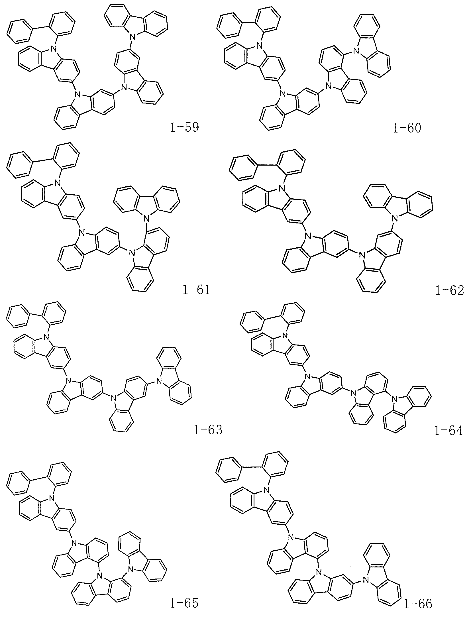


また、一般式(10)で表される化合物の具体的な例を以下に示すが、本発明はこれらの例示化合物に限定されるものではない。 Specific examples of compounds represented by general formula (10) are shown below, but the present invention is not limited to these exemplary compounds.

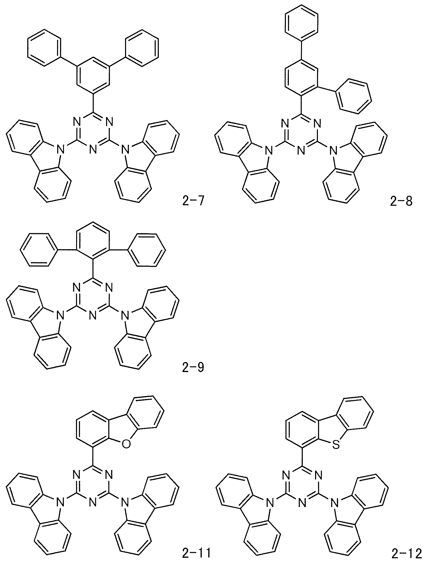


また、本発明は、対向する陽極と陰極の間に1つ以上の有機層を含む有機電界発光素子において、少なくとも1つの有機層が、前記一般式(1)で表される化合物、または、前記一般式(1)で表される化合物と前記一般式(10)で表される化合物を含む有機電界発光素子用混合材料を含有することを特徴とする有機電界発光素子であり、好ましくは、該有機層が、前記有機電界発光素子用混合材料を含有する有機電界発光素子である。 The present invention also relates to an organic electroluminescent device comprising one or more organic layers between opposing anodes and cathodes, characterized in that at least one of the organic layers contains a compound represented by the general formula (1) or a mixed material for organic electroluminescent devices comprising a compound represented by the general formula (1) and a compound represented by the general formula (10), and preferably the organic layer is an organic electroluminescent device comprising the mixed material for organic electroluminescent devices.
前記有機電界発光素子は、少なくとも1つの有機層が発光層であり、該発光層に前記有機電界発光素子用混合材料を含有させるのが好ましい。より好ましくは、該発光層中に、熱活性化遅延蛍光発光材料、又は燐光発光材料を更に含有させた有機電界発光素子であり、さらに好ましくは、該発光層中に熱活性化遅延蛍光発光材料を含有した有機電界発光素子である。また、前記熱活性化遅延蛍光発光材料はホウ素原子を含むものであるのが好ましく、前記燐光発光材料は白金原子を含むものであるのが好ましい。 The organic electroluminescent device preferably has at least one organic layer that is an emitting layer, and the emitting layer contains the mixed material for organic electroluminescent devices. More preferably, the emitting layer further contains a thermally activated delayed fluorescent material or a phosphorescent material, and even more preferably, the emitting layer contains a thermally activated delayed fluorescent material. In addition, the thermally activated delayed fluorescent material preferably contains boron atoms, and the phosphorescent material preferably contains platinum atoms.
すなわち、発光層には必要により、熱活性化遅延蛍光発光材料、又は燐光発光材料と共に少なくとも1つのホスト材料を含有させることにより優れた有機EL素子となるが、少なくとも1つのホスト材料が前記一般式(1)で表される化合物である有機電界発光素子用材料であるのが好ましい。また、該発光層に少なくとも2つのホスト材料を含有させる場合は、第1ホストとして前記一般式(1)で表される化合物と、第2ホストとして前記一般式(10)で表される化合物を用いるのが好ましい。 In other words, if necessary, the light-emitting layer can contain at least one host material together with the thermally activated delayed fluorescent material or phosphorescent material to produce an excellent organic EL device, and it is preferable that at least one host material is a material for organic electroluminescent devices that is a compound represented by the general formula (1). In addition, when the light-emitting layer contains at least two host materials, it is preferable to use a compound represented by the general formula (1) as the first host and a compound represented by the general formula (10) as the second host.
さらに、本発明は、対向する陽極と陰極の間に1つ以上の有機層を含む有機電界発光素子において、前記一般式(1)で表される化合物と、前記一般式(10)で表される環状アジン化合物とを事前に混合した有機電界発光素子用予備混合材料を用いて、一つの蒸着源から蒸着することで形成された発光層を有する有機電界発光素子及びその製造方法である。前記有機電界発光素子の有機層を作成するにあたり、前記有機電界発光素子用予備混合材料は、前記一般式(1)で表される化合物と前記一般式(10)で表される化合物をそれぞれ粉末にして事前に予備混合したものや、或いは、これらの粉末を加熱溶融により事前に予備混合したものこれを使用して、一つの蒸着源から蒸着することで有機EL素子の発光層を作製することができる。 Furthermore, the present invention relates to an organic electroluminescence device having one or more organic layers between opposing anodes and cathodes, and a method for producing the same, in which a light-emitting layer is formed by vapor deposition from a single vapor deposition source using a premixed material for organic electroluminescence devices in which a compound represented by the general formula (1) and a cyclic azine compound represented by the general formula (10) are mixed in advance. In producing the organic layer of the organic electroluminescence device, the premixed material for organic electroluminescence devices is a premix of the compound represented by the general formula (1) and the compound represented by the general formula (10) in powder form, or a premix of these powders by heating and melting them, and the premix is used to produce the light-emitting layer of the organic EL device by vapor deposition from a single vapor deposition source.
次に、本発明の有機EL素子の構造について、図面を参照しながら説明するが、本発明の有機EL素子の構造はこれに限定されない。 Next, the structure of the organic EL element of the present invention will be described with reference to the drawings, but the structure of the organic EL element of the present invention is not limited to this.
図1は、本発明に用いられる一般的な有機EL素子の構造例を示す断面図であり、1は基板、2は陽極、3は正孔注入層、4は正孔輸送層、5は発光層、6は電子輸送層、7は陰極を表す。本発明の有機EL素子では、陽極、発光層、そして陰極を必須の層として有するが、必須の層以外に正孔注入層、正孔輸送層、電子輸送層、電子注入層を有することがよく、更に正孔輸送層と発光層の間に電子阻止層、発光層と電子輸送層の間に正孔阻止層を有することができる。 Figure 1 is a cross-sectional view showing an example of the structure of a typical organic EL element used in the present invention, in which 1 is a substrate, 2 is an anode, 3 is a hole injection layer, 4 is a hole transport layer, 5 is an emitting layer, 6 is an electron transport layer, and 7 is a cathode. The organic EL element of the present invention has an anode, an emitting layer, and a cathode as essential layers, but may have a hole injection layer, a hole transport layer, an electron transport layer, and an electron injection layer in addition to the essential layers, and may further have an electron blocking layer between the hole transport layer and the emitting layer, and a hole blocking layer between the emitting layer and the electron transport layer.
図1とは逆の構造、すなわち基板1上に陰極7、電子輸送層6、発光層5、正孔輸送層4、正孔注入層3、陽極2の順に積層することも可能であり、この場合も必要により層を追加、省略することが可能である。なお、上述したような有機EL素子において、陽極や陰極のような電極以外に基板上で積層構造を構成する層をまとめて有機層という場合がある。 It is also possible to have the reverse structure to that shown in Figure 1, that is, to stack the cathode 7, electron transport layer 6, light-emitting layer 5, hole transport layer 4, hole injection layer 3, and anode 2 on the substrate 1 in that order, and in this case too, layers can be added or omitted as necessary. In the organic EL element described above, the layers that make up the stacked structure on the substrate other than the electrodes such as the anode and cathode are sometimes collectively referred to as organic layers.
-基板-
本発明の有機EL素子は、基板に支持されていることが好ましい。この基板については特に制限はなく、従来から有機EL素子に用いられているものであればよく、例えばガラス、透明プラスチック、石英等からなるものを用いることができる。
-substrate-
The organic EL element of the present invention is preferably supported by a substrate. There are no particular limitations on the substrate, and any substrate that has been conventionally used in organic EL elements, such as glass, transparent plastic, quartz, etc., can be used.
-陽極-
有機EL素子における陽極の材料としては、仕事関数の大きい(4eV以上)金属、合金、電気伝導性化合物又はこれらの混合物からなる材料が好ましく用いられる。このような電極材料の具体例としてはAu等の金属、CuI、インジウムチンオキシド(ITO)、SnO2、ZnO等の導電性透明材料が挙げられる。また、IDIXO(In2O3-ZnO)等の非晶質で、透明導電膜を作製可能な材料を用いてもよい。陽極はこれらの電極材料を蒸着やスパッタリング等の方法により薄膜を形成させ、フォトリソグラフィー法で所望の形状のパターンを形成してもよく、あるいはパターン精度をあまり必要としない場合(100μm以上程度)は、上記電極材料の蒸着やスパッタリング時に所望の形状のマスクを介してパターンを形成してもよい。あるいは有機導電性化合物のような塗布可能な物質を用いる場合には印刷方式、コーティング方式等湿式成膜法を用いることもできる。この陽極より発光を取り出す場合には、透過率を10%より大きくすることが望ましく、また、陽極としてのシート抵抗は数百Ω/□以下が好ましい。膜厚は材料にもよるが、通常10~1000nm、好ましくは10~200nmの範囲で選ばれる。
-anode-
As the material of the anode in the organic EL element, a material consisting of a metal, an alloy, an electrically conductive compound, or a mixture thereof having a large work function (4 eV or more) is preferably used. Specific examples of such electrode materials include metals such as Au, CuI, indium tin oxide (ITO), SnO 2 , ZnO, and other conductive transparent materials. In addition, amorphous materials such as IDIXO (In 2 O 3 -ZnO) that can be used to prepare a transparent conductive film may be used. The anode may be formed by forming a thin film of these electrode materials by a method such as vapor deposition or sputtering, and forming a pattern of a desired shape by a photolithography method, or when pattern accuracy is not required very much (about 100 μm or more), a pattern may be formed through a mask of a desired shape during vapor deposition or sputtering of the electrode material. Alternatively, when a coatable material such as an organic conductive compound is used, a wet film formation method such as a printing method or a coating method may be used. When light is to be emitted from this anode, it is desirable to make the transmittance greater than 10%, and the sheet resistance of the anode is preferably several hundred Ω/□ or less. The film thickness depends on the material, but is usually selected from the range of 10 to 1000 nm, preferably 10 to 200 nm.
-陰極-
一方、陰極の材料としては仕事関数の小さい(4eV以下)金属(電子注入性金属と称する)、合金、電気伝導性化合物又はこれらの混合物からなる材料が用いられる。このような電極材料の具体例としては、ナトリウム、ナトリウム-カリウム合金、マグネシウム、リチウム、マグネシウム/銅混合物、マグネシウム/銀混合物、マグネシウム/アルミニウム混合物、マグネシウム/インジウム混合物、アルミニウム/酸化アルミニウム(Al2O3)混合物、インジウム、リチウム/アルミニウム混合物、希土類金属等が挙げられる。これらの中で、電子注入性及び酸化等に対する耐久性の点から、電子注入性金属とこれより仕事関数の値が大きく安定な金属である第二金属との混合物、例えばマグネシウム/銀混合物、マグネシウム/アルミニウム混合物、マグネシウム/インジウム混合物、アルミニウム/酸化アルミニウム(Al2O3)混合物、リチウム/アルミニウム混合物、アルミニウム等が好適である。陰極はこれらの陰極材料を蒸着やスパッタリング等の方法により薄膜を形成させることにより、作製することができる。また、陰極としてシート抵抗は数百Ω/□以下が好ましく、膜厚は通常10nm~5μm、好ましくは50~200nmの範囲で選ばれる。なお、発光した光を透過させるため、有機EL素子の陽極又は陰極のいずれか一方が透明又は半透明であれば発光輝度は向上し、好都合である。
-cathode-
On the other hand, as the material of the cathode, a material consisting of a metal (referred to as an electron injecting metal), an alloy, an electrically conductive compound, or a mixture thereof having a small work function (4 eV or less) is used. Specific examples of such electrode materials include sodium, sodium-potassium alloy, magnesium, lithium, a magnesium/copper mixture, a magnesium/silver mixture, a magnesium/aluminum mixture, a magnesium/indium mixture, an aluminum/aluminum oxide (Al 2 O 3 ) mixture, indium, a lithium/aluminum mixture, and a rare earth metal. Among these, from the viewpoint of electron injectability and durability against oxidation, etc., a mixture of an electron injecting metal and a second metal which is a metal having a larger and more stable work function than the electron injecting metal, such as a magnesium/silver mixture, a magnesium/aluminum mixture, a magnesium/indium mixture, an aluminum/aluminum oxide (Al 2 O 3 ) mixture, a lithium/aluminum mixture, and aluminum, is preferable. The cathode can be produced by forming a thin film of these cathode materials by a method such as vapor deposition or sputtering. The sheet resistance of the cathode is preferably several hundred Ω/□ or less, and the film thickness is usually selected in the range of 10 nm to 5 μm, preferably 50 to 200 nm. In order to transmit the emitted light, it is advantageous for either the anode or the cathode of the organic EL element to be transparent or semi-transparent, as this improves the luminance of the emitted light.
また、陰極に上記金属を1~20nmの膜厚で形成した後に、陽極の説明で挙げた導電性透明材料をその上に形成することで、透明又は半透明の陰極を作製することができ、これを応用することで陽極と陰極の両方が透過性を有する素子を作製することができる。 In addition, after forming the above metals in a thickness of 1 to 20 nm on the cathode, a transparent or translucent cathode can be made by forming the conductive transparent material mentioned in the explanation of the anode on top of it. This can be used to create an element in which both the anode and cathode are transparent.
-発光層-
発光層は陽極及び陰極のそれぞれから注入された正孔及び電子が再結合することにより励起子が生成した後、発光する層であり、発光層は単一層でも複数層のどちらでもよく、それぞれ有機発光性ドーパント材料とホスト材料を含む。
-Light-emitting layer-
The light-emitting layer is a layer that emits light after excitons are generated by recombination of holes and electrons injected from the anode and cathode, respectively. The light-emitting layer may be either a single layer or multiple layers, and each layer contains an organic light-emitting dopant material and a host material.
有機発光性ドーパントは発光層中に1種類のみが含有されてもよく、2種類以上を含有してもよい。有機発光性ドーパントの含有量は、ホスト材料に対して0.1~50質量%であることが好ましく、0.1~40質量%であることがより好ましい。 The light-emitting layer may contain only one type of organic light-emitting dopant, or may contain two or more types. The content of the organic light-emitting dopant is preferably 0.1 to 50% by mass, and more preferably 0.1 to 40% by mass, relative to the host material.
有機発光性ドーパント材料として燐光発光ドーパントを使用する場合、燐光発光ドーパントとしては、ルテニウム、ロジウム、パラジウム、銀、レニウム、オスミウム、イリジウム、白金及び金から選ばれる少なくとも1つの金属を含む有機金属錯体を含有するものがよい。より好ましくは、白金を含む有機金属錯体であり、具体的には、J.Am.Chem.Soc.2001,123,4304や特表2013-530515号公報に記載されているイリジウム錯体やAdv. Mater.2014,26,7116や特開2018-2722号公報に記載されている白金錯体が好適に用いられるが、これらに限定されない。 When a phosphorescent dopant is used as the organic light-emitting dopant material, the phosphorescent dopant is preferably one that contains an organometallic complex containing at least one metal selected from ruthenium, rhodium, palladium, silver, rhenium, osmium, iridium, platinum, and gold. More preferably, it is an organometallic complex containing platinum, and specifically, the iridium complexes described in J.Am.Chem.Soc.2001,123,4304 and JP2013-530515A and the platinum complexes described in Adv.Mater.2014,26,7116 and JP2018-2722A are preferably used, but are not limited to these.
燐光発光ドーパント材料は、特に限定されるものではないが、具体的には以下のような例が挙げられる。 Phosphorescent dopant materials are not particularly limited, but specific examples include the following:


発光性ドーパント材料として蛍光発光ドーパントを使用する場合、蛍光発光ドーパントとしては、特に限定されないが、例えば縮合多環芳香族誘導体、スチリルアミン誘導体、縮合環アミン誘導体、ホウ素含有化合物、ピロール誘導体、インドール誘導体、カルバゾール誘導体等が挙げられる。これらの中でも、縮合環アミン誘導体、ホウ素含有化合物、カルバゾール誘導体が好ましい。縮合環アミン誘導体としては、例えば、ジアミンピレン誘導体、ジアミノクリセン誘導体、ジアミノアントラセン誘導体、ジアミノフルオレノン誘導体、ベンゾフロ骨格が1つ以上縮環したジアミノフルオレン誘導体等が挙げられる。
ホウ素含有化合物としては、例えば、ピロメテン誘導体やWO2015/102118号公報等に記載される多環芳香族化合物等が挙げられる。
When a fluorescent dopant is used as the light-emitting dopant material, the fluorescent dopant is not particularly limited, but examples thereof include condensed polycyclic aromatic derivatives, styrylamine derivatives, condensed ring amine derivatives, boron-containing compounds, pyrrole derivatives, indole derivatives, and carbazole derivatives. Among these, condensed ring amine derivatives, boron-containing compounds, and carbazole derivatives are preferred. Examples of condensed ring amine derivatives include diaminepyrene derivatives, diaminochrysene derivatives, diaminoanthracene derivatives, diaminofluorenone derivatives, and diaminofluorene derivatives having one or more condensed benzofuro skeletons.
Examples of the boron-containing compound include pyrromethene derivatives and polycyclic aromatic compounds described in WO2015/102118 and the like.
蛍光発光ドーパント材料は、特に限定されるものではないが、具体的には以下のような例が挙げられる。 The fluorescent dopant material is not particularly limited, but specific examples include the following:


発光性ドーパント材料として熱活性化遅延蛍光発光ドーパントを使用する場合、熱活性化遅延蛍光発光ドーパントとしては、特に限定されないが、ホウ素原子を含有したもの、スズ錯体や銅錯体等の金属錯体、Nature 2012,492,234に記載のシアノベンゼン誘導体、カルバゾール誘導体、Nature Photonics 2014,8,326に記載のフェナジン誘導体、オキサジアゾール誘導体、トリアゾール誘導体、スルホン誘導体、フェノキサジン誘導体、アクリジン誘導体、WO2015/102118号公報等に記載される多環芳香族化合物等が挙げられる。好ましくはホウ素原子を含む熱活性化遅延蛍光発光ドーパントである。 When a thermally activated delayed fluorescent dopant is used as the luminescent dopant material, examples of the thermally activated delayed fluorescent dopant include, but are not limited to, those containing boron atoms, metal complexes such as tin complexes and copper complexes, cyanobenzene derivatives described in Nature 2012,492,234, carbazole derivatives, phenazine derivatives described in Nature Photonics 2014,8,326, oxadiazole derivatives, triazole derivatives, sulfone derivatives, phenoxazine derivatives, acridine derivatives, and polycyclic aromatic compounds described in WO2015/102118, etc. Thermally activated delayed fluorescent dopants containing boron atoms are preferred.
熱活性化遅延蛍光発光ドーパント材料は、特に限定されるものではないが、具体的には以下のような例が挙げられる。熱活性化遅延蛍光発光ドーパント材料に環状アジン化合物を使用してもよいが、前記一般式(10)で表される化合物ではないことが好ましい。 The thermally activated delayed fluorescent dopant material is not particularly limited, but specific examples include the following. A cyclic azine compound may be used as the thermally activated delayed fluorescent dopant material, but it is preferable that it is not a compound represented by the general formula (10).

発光層におけるホスト材料としては、前記一般式(1)及び/又は一般式(10)で表される化合物を用いることが好ましい。前記一般式(1)や一般式(10)で表される化合物を発光層以外のいずれかの有機層で使用する場合、前記一般式(1)や一般式(10)で表される化合物を発光層に含んでも含まなくてもよい。この時、発光層には燐光発光素子や蛍光発光素子で使用される公知のホスト材料を併用することもできる。なお、公知のホスト材料を複数種併用して使用してもよいし、それぞれを単独で使用してもよい。使用できる公知のホスト材料としては、正孔輸送能、電子輸送能を有し、かつ高いガラス転移温度を有する化合物であり、発光性ドーパント材料の三重項励起エネルギー(T1)よりも大きい三重項励起エネルギー(T1)を有していることが好ましい。また、ホスト材料にTADF活性な化合物を用いてもよく、その場合、一重項励起エネルギー(S1)と三重項励起エネルギー(T1)の差(ΔEST = S1 - T1)が0.20eV以下の化合物が好ましい。また、前記一般式(1)で表される化合物を発光層に単独でホスト材料として含み、他の公知のホスト材料を併用してもよいが、有機EL素子の特性を向上させるためには、前記一般式(10)で表される化合物をホスト材料として併用するのが好ましい。なお、前記他の公知のホスト材料は、複数種類併用して用いてもよい。 As the host material in the light-emitting layer, it is preferable to use a compound represented by the general formula (1) and/or the general formula (10). When the compound represented by the general formula (1) or the general formula (10) is used in any organic layer other than the light-emitting layer, the compound represented by the general formula (1) or the general formula (10) may or may not be contained in the light-emitting layer. In this case, the light-emitting layer may be used in combination with a known host material used in phosphorescent or fluorescent light-emitting devices. Note that a combination of multiple known host materials may be used, or each may be used alone. The known host material that can be used is preferably a compound that has hole transporting ability and electron transporting ability and has a high glass transition temperature, and has a triplet excitation energy (T1) greater than the triplet excitation energy (T1) of the light-emitting dopant material. In addition, a TADF-active compound may be used as the host material, and in this case, a compound in which the difference between the singlet excitation energy (S1) and the triplet excitation energy (T1) (ΔEST = S1 - T1) is 0.20 eV or less is preferable. The compound represented by the general formula (1) may be used alone as a host material in the light-emitting layer, and other known host materials may be used in combination. However, in order to improve the characteristics of the organic EL device, it is preferable to use the compound represented by the general formula (10) in combination as a host material. Note that a plurality of types of the other known host materials may be used in combination.
ここで、S1、T1は次のようにして測定される。 石英基板上に真空蒸着法にて、真空度10-4Pa以下の条件にて試料化合物(熱活性化遅延蛍光材料)を蒸着し、蒸着膜を100nmの厚さで形成する。S1は、この蒸着膜の発光スペクトルを測定し、発光スペクトルの短波長側の立ち上がりに対して接線を引き、その接線と横軸の交点の波長値λedge[nm]を次に示す式(i)に代入してS1を算出する。
S1[eV]=1239.85/λedge (i)
Here, S1 and T1 are measured as follows. A sample compound (thermally activated delayed fluorescent material) is deposited on a quartz substrate by vacuum deposition under conditions of a vacuum degree of 10 −4 Pa or less to form a deposited film with a thickness of 100 nm. S1 is calculated by measuring the emission spectrum of this deposited film, drawing a tangent to the rising edge of the emission spectrum on the short wavelength side, and substituting the wavelength value λedge [nm] at the intersection of the tangent and the horizontal axis into the following formula (i):
S1[eV]=1239.85/λedge (i)
一方、T1は、前記蒸着膜の燐光スペクトルを測定し、この燐光スペクトルの短波長側の立ち上がりに対して接線を引き、その接線と横軸の交点の波長値λedge[nm]を下記の式(ii)に代入してT1を算出する。
T1[eV]=1239.85/λedge (ii)
On the other hand, T1 is calculated by measuring the phosphorescence spectrum of the evaporated film, drawing a tangent to the rising edge on the short wavelength side of the phosphorescence spectrum, and substituting the wavelength value λedge [nm] at the intersection of the tangent and the horizontal axis into the following formula (ii).
T1[eV]=1239.85/λedge (ii)
前記他の公知のホスト材料は、多数の特許文献等により知られているものから選択することができる。ホスト材料の具体例としては、特に限定されるものではないが、インドール化合物、カルバゾール化合物、ピリジン化合物、ピリミジン化合物、トリアジン化合物、トリアゾール化合物、オキサゾール化合物、オキサジアゾール化合物、イミダゾール化合物、フェニレンジアミン化合物、アリールアミン化合物、アントラセン化合物、フルオレノン化合物、スチルベン化合物、トリフェニレン化合物、カルボラン化合物、ポルフィリン化合物、フタロシアニン化合物、8-キノリノール化合物の金属錯体やメタルフタロシアニン、ベンゾオキサゾールやベンゾチアゾール化合物の金属錯体に代表される各種金属錯体、ポリ(N-ビニルカルバゾール)化合物、アニリン系共重合化合物、チオフェンオリゴマー、ポリチオフェン化合物、ポリフェニレン化合物、ポリフェニレンビニレン化合物、ポリフルオレン化合物等の高分子化合物等が挙げられる。好ましくは、カルバゾール化合物、インドロカルバゾール化合物、ピリジン化合物、ピリミジン化合物、トリアジン化合物、アントラセン化合物、トリフェニレン化合物、カルボラン化合物、ポルフィリン化合物が挙げられる。 The other known host materials can be selected from those known in numerous patent documents, etc. Specific examples of host materials include, but are not limited to, indole compounds, carbazole compounds, pyridine compounds, pyrimidine compounds, triazine compounds, triazole compounds, oxazole compounds, oxadiazole compounds, imidazole compounds, phenylenediamine compounds, arylamine compounds, anthracene compounds, fluorenone compounds, stilbene compounds, triphenylene compounds, carborane compounds, porphyrin compounds, phthalocyanine compounds, metal complexes of 8-quinolinol compounds, metal phthalocyanines, various metal complexes represented by metal complexes of benzoxazole and benzothiazole compounds, poly(N-vinylcarbazole) compounds, aniline copolymer compounds, thiophene oligomers, polythiophene compounds, polyphenylene compounds, polyphenylenevinylene compounds, polyfluorene compounds, and other polymeric compounds. Preferred examples include carbazole compounds, indolocarbazole compounds, pyridine compounds, pyrimidine compounds, triazine compounds, anthracene compounds, triphenylene compounds, carborane compounds, and porphyrin compounds.
前記他の公知のホストとしては、特に限定されるものではないが、具体的には以下のような化合物が挙げられる。


ホストを複数種使用する場合は、それぞれのホストを異なる蒸着源から蒸着するか、蒸着前に予備混合して予備混合材料とすることで1つの蒸着源から複数種のホストを同時に蒸着することもできる。 When using multiple types of hosts, each host can be evaporated from a different evaporation source, or they can be premixed before evaporation to form a premixed material, allowing multiple hosts to be evaporated simultaneously from a single evaporation source.
ホストを複数種使用する場合、ホストは前記一般式(1)で表される化合物と前記一般式(10)で表される化合物とを混合することにより得られる前記有機電界発光素子用混合材料であることが好ましい。 When multiple types of hosts are used, the host is preferably a mixed material for organic electroluminescent devices obtained by mixing a compound represented by the general formula (1) and a compound represented by the general formula (10).
2種類のホストを予備混合して使用する場合は、良好な特性を有する有機EL素子を再現性良く作製するために、互いの50%重量減少温度(T50)の差が小さいことが望ましい。50%重量減少温度は、窒素気流減圧(1Pa)下でのTG-DTA測定において、室温から毎分10℃の速度で550℃まで昇温したとき、重量が50%減少した際の温度をいう。この温度付近では、蒸発又は昇華による気化が最も盛んに起こると考えられる。 When two types of hosts are premixed and used, it is desirable that the difference between their 50% weight loss temperatures (T 50 ) is small in order to reproducibly fabricate organic EL devices with good characteristics. The 50% weight loss temperature is the temperature at which the weight is reduced by 50% when the temperature is raised from room temperature to 550°C at a rate of 10°C per minute in TG-DTA measurement under reduced pressure (1 Pa) of nitrogen gas flow. It is believed that vaporization by evaporation or sublimation occurs most actively around this temperature.
予備混合材料における2種類のホストの50%重量減少温度の差が20℃以内であることが好ましい。この予備混合物を単一の蒸発源から気化させて蒸着することで、均一な蒸着膜を得ることが可能となる。この際、予備混合物には、発光層を形成するために必要な発光性ドーパント材料又は必要により使用される他のホストを混合させてもよいが、所望の蒸気圧となる温度に大きな差がある場合は、別の蒸着源から蒸着させることがよい。 The difference in 50% weight loss temperature between the two types of hosts in the premixed material is preferably within 20°C. By vaporizing and depositing this premix from a single evaporation source, it is possible to obtain a uniform deposited film. In this case, the premix may be mixed with a luminescent dopant material required to form a light-emitting layer or other hosts to be used as necessary, but if there is a large difference in the temperature at which the desired vapor pressure is achieved, it is better to deposit from separate evaporation sources.
また、ホストを2種類使用する場合の第1ホストと第2ホストの混合比(質量比)は、第1ホストと第2ホストの合計に対し、第1ホストの割合が40~90%がよく、好ましくは50~90%であり、より好ましくは60~90%である。前記一般式(1)で表される化合物と前記前記一般式(10)で表される化合物をホストとして用いる場合、第1ホストが前記一般式(1)で表される化合物となり、前記一般式(10)で表される化合物が第2ホストとなる。 In addition, when two types of hosts are used, the mixing ratio (mass ratio) of the first host to the second host is preferably 40 to 90%, more preferably 50 to 90%, and even more preferably 60 to 90% of the first host relative to the total of the first host and the second host. When the compound represented by the general formula (1) and the compound represented by the general formula (10) are used as hosts, the first host is the compound represented by the general formula (1), and the compound represented by the general formula (10) is the second host.
前述したように、ホストの予備混合の方法としては可及的に均一に混合できる方法が望ましく、粉砕混合や、減圧下又は窒素のような不活性ガス雰囲気下で加熱溶融させる方法や、昇華等が挙げられるが、これらの方法に限定されるものではない。 As mentioned above, the method for premixing the host is preferably one that allows for as uniform mixing as possible, and examples of such methods include pulverization and mixing, heating and melting under reduced pressure or in an inert gas atmosphere such as nitrogen, and sublimation, but are not limited to these.
また、ホスト、及びその予備混合物の形態は、粉体、スティック状、または顆粒状であってもよい。 The host and its premixture may also be in the form of a powder, stick, or granules.
-注入層-
注入層とは、駆動電圧低下や発光輝度向上のために電極と有機層間に設けられる層のことで、正孔注入層と電子注入層があり、陽極と発光層又は正孔輸送層の間、及び陰極と発光層又は電子輸送層との間に存在させてもよい。注入層は必要に応じて設けることができる。
-Injection layer-
The injection layer is a layer provided between an electrode and an organic layer to reduce the driving voltage and improve the luminance of light emitted, and includes a hole injection layer and an electron injection layer, and may be provided between the anode and the light emitting layer or the hole transport layer, and between the cathode and the light emitting layer or the electron transport layer. The injection layer can be provided as necessary.
-正孔阻止層-
正孔阻止層とは広い意味では電子輸送層の機能を有し、電子を輸送する機能を有しつつ正孔を輸送する能力が著しく小さい正孔阻止材料からなり、電子を輸送しつつ正孔を阻止することで発光層中での電子と正孔の再結合確率を向上させることができる。正孔阻止層には、公知の正孔阻止材料をすることができる。また正孔阻止材料を複数種類併用して用いてもよい。
-Hole blocking layer-
In a broad sense, the hole blocking layer has the function of an electron transport layer, and is made of a hole blocking material that has the function of transporting electrons but has a significantly small ability to transport holes, and can improve the probability of recombination of electrons and holes in the light emitting layer by blocking holes while transporting electrons. The hole blocking layer can be made of a known hole blocking material. A plurality of hole blocking materials may also be used in combination.
-電子阻止層-
電子阻止層とは広い意味では正孔輸送層の機能を有し、正孔を輸送しつつ電子を阻止することで発光層中での電子と正孔が再結合する確率を向上させることができる。電子阻止層の材料としては、前記一般式(1)で表される化合物、又は前記混合材料を用いることが好ましいが、公知の電子阻止層材料を用いることもできる。なお、前記一般式(1)で表される化合物、又は前記混合材料を電子阻止層に用いる場合は、ホスト材料として前記一般式(1)で表される化合物、上記で述べた公知のホスト材料、及びこれらを複数種組み合わせたホスト材料を使用してもよい。
-Electron blocking layer-
In a broad sense, the electron blocking layer has the function of a hole transport layer, and by blocking electrons while transporting holes, the probability of electrons and holes recombining in the light emitting layer can be improved. As the material of the electron blocking layer, it is preferable to use the compound represented by the general formula (1) or the mixed material, but a known electron blocking layer material can also be used. When the compound represented by the general formula (1) or the mixed material is used in the electron blocking layer, the compound represented by the general formula (1), the known host material described above, and a host material obtained by combining a plurality of these may be used as the host material.
発光層に隣接する層としては、正孔阻止層、電子阻止層などがあるが、これらの層が設けられない場合は、正孔輸送層、電子輸送層などが隣接層となる。 Layers adjacent to the light-emitting layer include a hole-blocking layer and an electron-blocking layer, but if these layers are not provided, the adjacent layers will be a hole-transporting layer and an electron-transporting layer.
-正孔輸送層-
正孔輸送層とは正孔を輸送する機能を有する正孔輸送材料からなり、正孔輸送層は単層又は複数層設けることができる。
-Hole transport layer-
The hole transport layer is made of a hole transport material having a function of transporting holes, and the hole transport layer may be provided as a single layer or multiple layers.
正孔輸送材料としては、正孔の注入、又は輸送、電子の障壁性のいずれかを有するものであり、有機物、無機物のいずれであってもよい。正孔輸送材料としては、従来公知の化合物の中から任意のものを選択して用いることができる。かかる正孔輸送材料としては例えば、ポルフィリン誘導体、アリールアミン誘導体、トリアゾール誘導体、オキサジアゾール誘導体、イミダゾール誘導体、ポリアリールアルカン誘導体、フェニレンジアミン誘導体、アリールアミン誘導体、アミノ置換カルコン誘導体、オキサゾール誘導体、スチリルアントラセン誘導体、フルオレノン誘導体、ヒドラゾン誘導体、スチルベン誘導体、シラザン誘導体、アニリン系共重合体、また導電性高分子オリゴマー、特にチオフェンオリゴマー等が挙げられる。 The hole transport material has either hole injection or transport properties or electron barrier properties, and may be either organic or inorganic. Any hole transport material may be selected from conventionally known compounds. Examples of such hole transport materials include porphyrin derivatives, arylamine derivatives, triazole derivatives, oxadiazole derivatives, imidazole derivatives, polyarylalkane derivatives, phenylenediamine derivatives, arylamine derivatives, amino-substituted chalcone derivatives, oxazole derivatives, styrylanthracene derivatives, fluorenone derivatives, hydrazone derivatives, stilbene derivatives, silazane derivatives, aniline-based copolymers, and conductive polymer oligomers, particularly thiophene oligomers.
-電子輸送層-
電子輸送層とは電子を輸送する機能を有する材料からなり、電子輸送層は単層又は複数層設けることができる。
-Electron transport layer-
The electron transport layer is made of a material having a function of transporting electrons, and the electron transport layer may be provided as a single layer or as a multi-layer.
電子輸送材料(正孔阻止材料を兼ねる場合もある)としては、陰極より注入された電子を発光層に伝達する機能を有していればよい。電子輸送層には、従来公知の化合物の中から任意のものを選択して用いることができ、例えば、ナフタレン、アントラセン、フェナントロリン等の多環芳香族誘導体、トリス(8-キノリノラート)アルミニウム(III)誘導体、ホスフィンオキサイド誘導体、ニトロ置換フルオレン誘導体、ジフェニルキノン誘導体、チオピランジオキシド誘導体、カルボジイミド、フレオレニリデンメタン誘導体、アントラキノジメタン及びアントロン誘導体、ビピリジン誘導体、キノリン誘導体、オキサジアゾール誘導体、ベンゾイミダゾール誘導体、ベンゾチアゾール誘導体、インドロカルバゾール誘導体等が挙げられる。更にこれらの材料を高分子鎖に導入した、又はこれらの材料を高分子の主鎖とした高分子材料を用いることもできる。 The electron transport material (which may also serve as a hole blocking material) may have the function of transmitting electrons injected from the cathode to the light emitting layer. For the electron transport layer, any of the conventionally known compounds may be selected and used, such as polycyclic aromatic derivatives such as naphthalene, anthracene, and phenanthroline, tris(8-quinolinolato)aluminum(III) derivatives, phosphine oxide derivatives, nitro-substituted fluorene derivatives, diphenylquinone derivatives, thiopyran dioxide derivatives, carbodiimides, fluorenylidenemethane derivatives, anthraquinodimethane and anthrone derivatives, bipyridine derivatives, quinoline derivatives, oxadiazole derivatives, benzimidazole derivatives, benzothiazole derivatives, and indolocarbazole derivatives. Furthermore, polymeric materials in which these materials are introduced into the polymer chain or in which these materials form the polymer main chain may also be used.
本発明の有機EL素子を作製する際の、各層の製膜方法は特に限定されず、ドライプロセス、ウェットプロセスのどちらで作製してもよい。 When producing the organic EL element of the present invention, there are no particular limitations on the method for forming each layer, and they may be produced by either a dry process or a wet process.
以下、本発明を実施例によって更に詳しく説明するが、本発明はこれらの実施例に限定されるものではない。 The present invention will be explained in more detail below with reference to examples, but the present invention is not limited to these examples.
代表例として、化合物1-119の合成例を示す。他の化合物についても、類似の方法で合成した。なお、式中のDnは、それぞれの化合物ごとに独立に、化合物の一部若しくは全部の水素が重水素化していることを示す。
As a representative example, the synthesis of compound 1-119 is shown below. Other compounds were synthesized in a similar manner. Note that Dn in the formula indicates that some or all of the hydrogen atoms in the compound are deuterated, independently for each compound.
合成例1

Synthesis Example 1
合成例2

実施例及び比較例で用いた化合物を以下に示す。
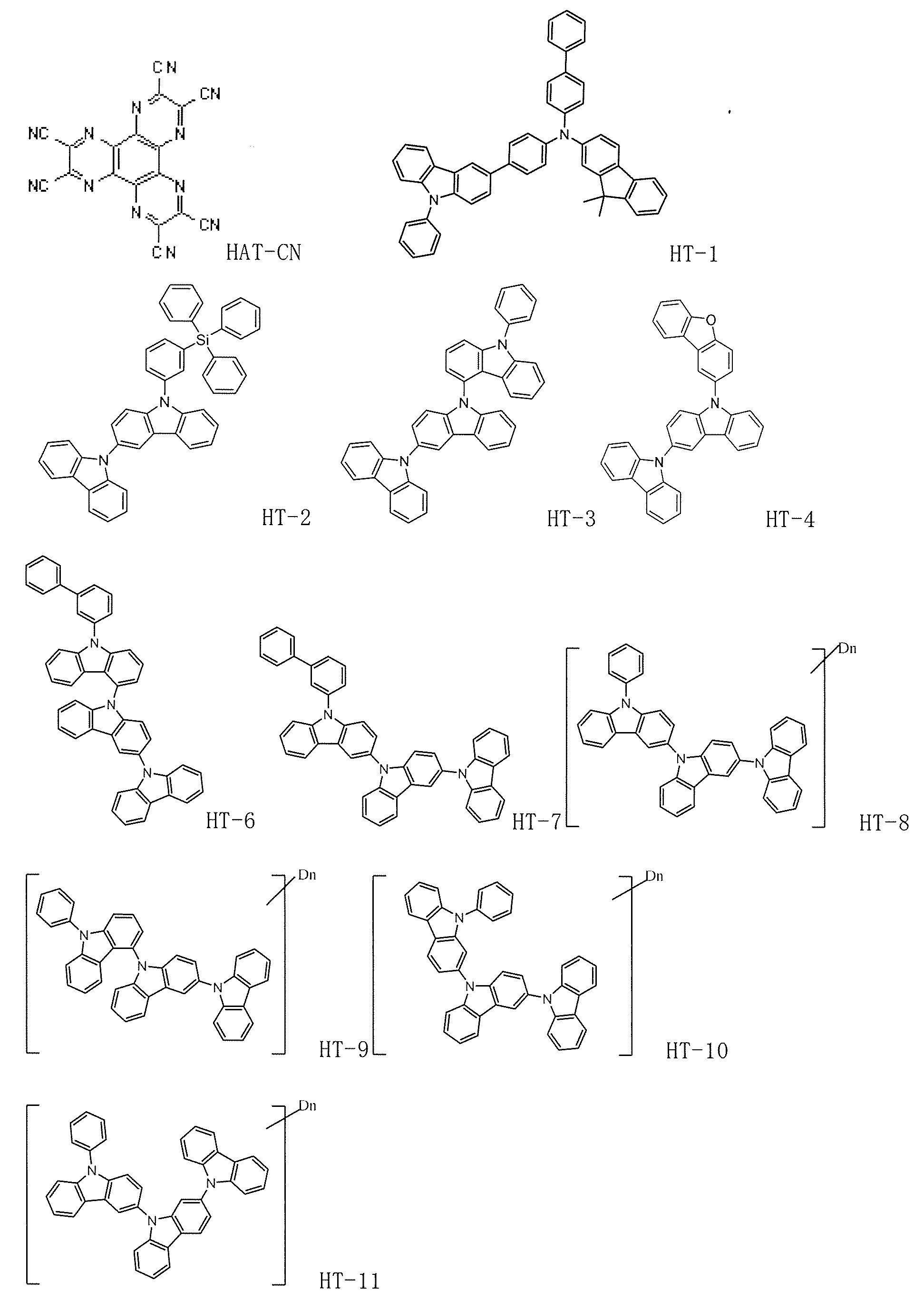

実施例1
膜厚70nmのITOからなる陽極が形成されたガラス基板上に、以下に示す各薄膜を真空蒸着法にて、真空度4.0×10⁻⁵Paで積層した。先ず、ITO上に正孔注入層として先に示したHAT-CNを10nmの厚さに形成し、次に、正孔輸送層としてHT-1を60nmの厚さに形成した。次に、電子阻止層としてHT-2を5nmの厚さに形成した。次に、ホストとして化合物(1-12)を、燐光発光ドーパントとしてBD-2を、熱活性化遅延蛍光発光ドーパントとしてBD-1をそれぞれ異なる蒸着源から共蒸着し、40nmの厚さを有する発光層を形成した。この時、BD-2の濃度が13質量%、BD-1の濃度が0.4質量%、1-12を86.6質量%となる蒸着条件で共蒸着した。次に、正孔阻止層としてET-2を5nmの厚さに形成した。次に、電子輸送層としてET-2を31nmの厚さに形成した。更に、電子輸送層上に電子注入層としてフッ化リチウム(LiF)を1nmの厚さに形成した。最後に、電子注入層上に陰極としてアルミニウム(Al)を70nmの厚さに形成し、実施例1に係る有機EL素子を作製した。
Example 1
On a glass substrate on which an anode made of ITO having a film thickness of 70 nm was formed, each of the thin films shown below was laminated at a vacuum degree of 4.0×10 −5 Pa by vacuum deposition. First, HAT-CN shown above was formed on ITO as a hole injection layer to a thickness of 10 nm, and then HT-1 was formed as a hole transport layer to a thickness of 60 nm. Next, HT-2 was formed as an electron blocking layer to a thickness of 5 nm. Next, compound (1-12) was co-deposited as a host, BD-2 as a phosphorescent dopant, and BD-1 as a thermally activated delayed fluorescent dopant from different deposition sources to form an emission layer having a thickness of 40 nm. At this time, the co-deposition was performed under deposition conditions in which the concentration of BD-2 was 13% by mass, the concentration of BD-1 was 0.4% by mass, and 1-12 was 86.6% by mass. Next, ET-2 was formed as a hole blocking layer to a thickness of 5 nm. Next, ET-2 was formed as an electron transport layer to a thickness of 31 nm. Furthermore, lithium fluoride (LiF) was formed as an electron injection layer to a thickness of 1 nm on the electron transport layer. Finally, aluminum (Al) was formed as a cathode to a thickness of 70 nm on the electron injection layer, thereby producing the organic EL element according to Example 1.
比較例1
表1に示したように、ホストをHT-2とした以外は、実施例1と同様にして有機EL素子を作製した。
Comparative Example 1
As shown in Table 1, an organic EL device was prepared in the same manner as in Example 1, except that the host was changed to HT-2.
実施例2~9
電子阻止層材料、第1ホストを表1に示す化合物とした以外は、実施例1と同様にして有機EL素子を作製した。
Examples 2 to 9
Organic EL devices were prepared in the same manner as in Example 1, except that the electron blocking layer material and the first host were the compounds shown in Table 1.
実施例10
膜厚70nmのITOからなる陽極が形成されたガラス基板上に、以下に示す各薄膜を真空蒸着法にて、真空度4.0×10⁻⁵Paで積層した。先ず、ITO上に正孔注入層として先に示したHAT-CNを10nmの厚さに形成し、次に、正孔輸送層としてHT-1を60nmの厚さに形成した。次に、電子阻止層としてHT-2を5nmの厚さに形成した。次に、第1ホストとして化合物(1-6)を、第2ホストとして化合物(2-49)を、燐光発光ドーパントとしてBD-2を、熱活性化遅延蛍光発光ドーパントとしてBD-1をそれぞれ異なる蒸着源から共蒸着し、40nmの厚さを有する発光層を形成した。この時、BD-2の濃度が13質量%、BD-1の濃度が0.4質量%、第1ホストと第2ホストの質量比が50:50となる蒸着条件で共蒸着した。次に、正孔阻止層としてET-2を5nmの厚さに形成した。次に電子輸送層としてET-2を31nmの厚さに形成した。更に、電子輸送層上に電子注入層としてフッ化リチウム(LiF)を1nmの厚さに形成した。最後に、電子注入層上に陰極としてアルミニウム(Al)を70nmの厚さに形成し、実施例2に係る有機EL素子を作製した。
Example 10
On a glass substrate on which an anode made of ITO having a thickness of 70 nm was formed, each of the thin films shown below was laminated by vacuum deposition at a vacuum degree of 4.0×10 −5 Pa. First, HAT-CN shown above was formed on ITO as a hole injection layer to a thickness of 10 nm, and then HT-1 was formed as a hole transport layer to a thickness of 60 nm. Next, HT-2 was formed as an electron blocking layer to a thickness of 5 nm. Next, compound (1-6) was co-deposited as a first host, compound (2-49) was co-deposited as a second host, BD-2 was co-deposited as a phosphorescent dopant, and BD-1 was co-deposited as a thermally activated delayed fluorescent dopant from different deposition sources to form an emitting layer having a thickness of 40 nm. At this time, the co-deposition was performed under deposition conditions where the concentration of BD-2 was 13% by mass, the concentration of BD-1 was 0.4% by mass, and the mass ratio of the first host to the second host was 50:50. Next, ET-2 was formed to a thickness of 5 nm as a hole blocking layer. Next, ET-2 was formed to a thickness of 31 nm as an electron transport layer. Furthermore, lithium fluoride (LiF) was formed to a thickness of 1 nm as an electron injection layer on the electron transport layer. Finally, aluminum (Al) was formed to a thickness of 70 nm as a cathode on the electron injection layer, thereby producing an organic EL device according to Example 2.
実施例11~32、実施例A-1~A-6、比較例2~10、比較例A-1~A-4
電子阻止層材料、第1ホスト、及び第2ホストを表1又は表2に示す化合物とした以外は、実施例10と同様にして有機EL素子を作製した。なお、化合物(1-118)、(1-119)、(1-120)、(1-121)、(1-122)、(1-123)、(1-124)、(1-125)、(1-126)、(1-127)、(1-128)、(1-129)の平均重水素化率は、それぞれ26%、85%、88%、90%、83%、89%、86%、90%、87%、83%、82%、84%である材料を使用した。また、化合物HT-8、HT-9、HT-10、HT-11の平均重水素化率は、それぞれ86%、86%、88%、87%である材料を使用した。平均重水素化率は、前記化合物に含まれる水素が重水素化されている割合を示すものであり、質量分析法又はプロトン核磁気共鳴分光法によって求めた。
Examples 11 to 32, Examples A-1 to A-6, Comparative Examples 2 to 10, Comparative Examples A-1 to A-4
Organic EL devices were prepared in the same manner as in Example 10, except that the electron blocking layer material, the first host, and the second host were the compounds shown in Table 1 or Table 2. The compounds (1-118), (1-119), (1-120), (1-121), (1-122), (1-123), (1-124), (1-125), (1-126), (1-127), (1-128), and (1-129) had average deuteration ratios of 26%, 85%, 88%, 90%, 83%, 89%, 86%, 90%, 87%, 83%, 82%, and 84%, respectively. The compounds HT-8, HT-9, HT-10, and HT-11 had average deuteration ratios of 86%, 86%, 88%, and 87%, respectively. The average deuteration ratio indicates the ratio of hydrogen contained in the compound that is deuterium-substituted, and was determined by mass spectrometry or proton nuclear magnetic resonance spectroscopy.
例えばプロトン核磁気共鳴分光法によって平均重水素化率を求める場合は、まず重溶媒に化合物、及び内部標準物質を添加し溶解することで測定試料を調製し、内部標準物質と化合物由来の積分強度比から、測定試料中に含まれる化合物のプロトン濃度[mol/g]を計算する。次に、重水素化合物のプロトン濃度と、それに対応する重水素化されていない化合物のプロトン濃度の比を計算し、1から減じることで重水素化合物の平均重水素化率を算出することができる。また、部分構造の平均重水素化率は、対象の部分構造に由来する化学シフトの積分強度から、前記同様の手順で算出できる。化合物1-118について、プロトン核磁気共鳴分光法によって平均重水素化率を求めた方法を以下に示す。まず重水素化テトラヒドロフラン(1.0ml)に化合物1-118(5.0mg)及び内部標準物質としてジメチルスルホン(2.0mg)を溶解することで、測定試料を調製した。内部標準物質と化合物1-118由来の積分強度比から、測定試料中に含まれる化合物1-118の平均のプロトン濃度[mol/g]を計算した。また、化合物1-118の非重水素化体(例示化合物1-15に該当)についても同様に平均のプロトン濃度[mol/g]を計算した。次に、化合物1-118のプロトン濃度と化合物1-118の非重水素化体のプロトン濃度の比を計算し、1から減じることで化合物1-118の平均重水素化率を算出した。 For example, when determining the average deuteration ratio by proton nuclear magnetic resonance spectroscopy, a measurement sample is prepared by adding and dissolving the compound and an internal standard in a deuterated solvent, and the proton concentration [mol/g] of the compound contained in the measurement sample is calculated from the integrated intensity ratio of the internal standard and the compound. Next, the ratio of the proton concentration of the deuterated compound to the proton concentration of the corresponding non-deuterated compound is calculated, and the average deuteration ratio of the deuterated compound can be calculated by subtracting it from 1. The average deuteration ratio of a partial structure can be calculated from the integrated intensity of the chemical shift derived from the target partial structure in the same manner as above. The method for determining the average deuteration ratio of compound 1-118 by proton nuclear magnetic resonance spectroscopy is shown below. First, a measurement sample was prepared by dissolving compound 1-118 (5.0 mg) and dimethyl sulfone (2.0 mg) as an internal standard in deuterated tetrahydrofuran (1.0 ml). The average proton concentration [mol/g] of compound 1-118 contained in the measurement sample was calculated from the integrated intensity ratio of the internal standard and compound 1-118. The average proton concentration [mol/g] was also calculated in the same manner for the non-deuterated form of compound 1-118 (corresponding to example compound 1-15). Next, the ratio of the proton concentration of compound 1-118 to the proton concentration of the non-deuterated form of compound 1-118 was calculated, and this was subtracted from 1 to calculate the average deuteration rate of compound 1-118.


作製した有機EL素子の評価結果を表3及び表4に示す。実施例及び比較例で得られた有機EL素子に外部電源を接続し直流電圧を印加したところ、すべての有機EL素子において、極大発光波長450nm~480nmの発光スペクトルが観測され、BD-1からの発光が得られていることがわかった。
表中の電圧、電力効率は駆動電流2.5mA/cm2時の値であり、初期特性である。また、寿命は、駆動電流4.0mA/cm2における初期輝度を100%とした際、輝度が97%に減衰するまでにかかる時間であり、寿命特性を表す。また、発光色は有機EL素子の発光スペクトルにて確認したものである。表3及び表4に示した実施例と比較例の結果より、発光層中にホストとして本発明の有機電界発光素子用混合材料を用いた有機EL素子は、青色発光であり、低電圧、高効率、長寿命な特性を有することが分かる。
The evaluation results of the produced organic EL elements are shown in Tables 3 and 4. When an external power source was connected to the organic EL elements obtained in the Examples and Comparative Examples and a DC voltage was applied, an emission spectrum with a maximum emission wavelength of 450 nm to 480 nm was observed in all the organic EL elements, indicating that light emission was obtained from BD-1.
The voltage and power efficiency in the table are values at a driving current of 2.5 mA/cm2, which are initial characteristics. The lifetime is the time it takes for the brightness to decay to 97% when the initial brightness at a driving current of 4.0 mA/cm2 is taken as 100%, and represents the lifetime characteristics. The emission color was confirmed by the emission spectrum of the organic EL element. From the results of the examples and comparative examples shown in Tables 3 and 4, it can be seen that the organic EL element using the mixed material for organic electroluminescent element of the present invention as a host in the emission layer emits blue light and has low voltage, high efficiency, and long lifetime characteristics.


実施例33
膜厚70nmのITOからなる陽極が形成されたガラス基板上に、以下に示す各薄膜を真空蒸着法にて、真空度4.0×10⁻⁵Paで積層した。先ず、ITO上に正孔注入層として先に示したHAT-CNを10nmの厚さに形成し、次に、正孔輸送層としてHT-1を60nmの厚さに形成した。次に、電子阻止層としてHT-2を5nmの厚さに形成した。次に、第1ホストとして化合物(1-12)を、燐光発光ドーパントとしてBD-2をそれぞれ異なる蒸着源から共蒸着し、40nmの厚さを有する発光層を形成した。この時、BD-2の濃度が13質量%となる蒸着条件で共蒸着した。次に、正孔阻止層としてET-2を5nmの厚さに形成した。次に電子輸送層としてET-2を31nmの厚さに形成した。更に、電子輸送層上に電子注入層としてフッ化リチウム(LiF)を1nmの厚さに形成した。最後に、電子注入層上に陰極としてアルミニウム(Al)を70nmの厚さに形成し、比較例9に係る有機EL素子を作製した。
Example 33
On a glass substrate on which an anode made of ITO with a film thickness of 70 nm was formed, each of the thin films shown below was laminated by vacuum deposition at a vacuum degree of 4.0×10 −5 Pa. First, HAT-CN shown above was formed on ITO as a hole injection layer with a thickness of 10 nm, and then HT-1 was formed as a hole transport layer with a thickness of 60 nm. Next, HT-2 was formed as an electron blocking layer with a thickness of 5 nm. Next, compound (1-12) was co-deposited as a first host and BD-2 was co-deposited as a phosphorescent dopant from different deposition sources to form a light-emitting layer having a thickness of 40 nm. At this time, the co-deposition was performed under deposition conditions in which the concentration of BD-2 was 13% by mass. Next, ET-2 was formed as a hole blocking layer with a thickness of 5 nm. Next, ET-2 was formed as an electron transport layer with a thickness of 31 nm. Furthermore, lithium fluoride (LiF) was formed as an electron injection layer on the electron transport layer with a thickness of 1 nm. Finally, aluminum (Al) was formed as a cathode to a thickness of 70 nm on the electron injection layer, thereby completing the organic EL element according to Comparative Example 9.
実施例34~41、比較例11
表5に示したように、第1ホストを表5に示す化合物とした以外は、実施例33と同様にして有機EL素子を作製した。
Examples 34 to 41, Comparative Example 11
As shown in Table 5, an organic EL device was prepared in the same manner as in Example 33, except that the first host was a compound shown in Table 5.
実施例42
膜厚70nmのITOからなる陽極が形成されたガラス基板上に、以下に示す各薄膜を真空蒸着法にて、真空度4.0×10⁻⁵Paで積層した。先ず、ITO上に正孔注入層として先に示したHAT-CNを10nmの厚さに形成し、次に、正孔輸送層としてHT-1を60nmの厚さに形成した。次に、電子阻止層としてHT-2を5nmの厚さに形成した。次に、第1ホストとして化合物(1-12)を、第2ホストとして化合物(2-49)を、燐光発光ドーパントとしてBD-2をそれぞれ異なる蒸着源から共蒸着し、40nmの厚さを有する発光層を形成した。この時、BD-2の濃度が13質量%となる蒸着条件で共蒸着した。次に、正孔阻止層としてET-2を5nmの厚さに形成した。次に電子輸送層としてET-2を31nmの厚さに形成した。更に、電子輸送層上に電子注入層としてフッ化リチウム(LiF)を1nmの厚さに形成した。最後に、電子注入層上に陰極としてアルミニウム(Al)を70nmの厚さに形成し、実施例42に係る有機EL素子を作製した。
Example 42
On a glass substrate on which an anode made of ITO having a thickness of 70 nm was formed, each of the thin films shown below was laminated by vacuum deposition at a vacuum degree of 4.0×10 −5 Pa. First, HAT-CN shown above was formed on ITO as a hole injection layer to a thickness of 10 nm, and then HT-1 was formed as a hole transport layer to a thickness of 60 nm. Next, HT-2 was formed as an electron blocking layer to a thickness of 5 nm. Next, compound (1-12) was co-deposited as a first host, compound (2-49) was co-deposited as a second host, and BD-2 was co-deposited as a phosphorescent dopant from different deposition sources to form a light-emitting layer having a thickness of 40 nm. At this time, the co-deposition was performed under deposition conditions in which the concentration of BD-2 was 13% by mass. Next, ET-2 was formed as a hole blocking layer to a thickness of 5 nm. Next, ET-2 was formed as an electron transport layer to a thickness of 31 nm. Furthermore, lithium fluoride (LiF) was formed as an electron injection layer to a thickness of 1 nm on the electron transport layer, and finally, aluminum (Al) was formed as a cathode to a thickness of 70 nm on the electron injection layer to prepare an organic EL device according to Example 42.
実施例43~64、比較例12~18
電子阻止層材料、第1ホスト、及び第2ホストを表5に示す化合物とした以外は、実施例42と同様にして有機EL素子を作製した。
Examples 43 to 64, Comparative Examples 12 to 18
An organic EL device was prepared in the same manner as in Example 42, except that the electron blocking layer material, the first host, and the second host were each formed as the compounds shown in Table 5.

作製した有機EL素子の評価結果を表6に示す。表中の電圧、電力効率は駆動電流2.5mA/cm2時の値であり、初期特性である。また、寿命は、駆動電流4.0mA/cm2における初期輝度を100%とした際、輝度が97%に減衰するまでにかかる時間であり、寿命特性を表す。また、発光色は有機EL素子の発光スペクトルにて確認したものである。 The evaluation results of the organic EL elements produced are shown in Table 6. The voltage and power efficiency in the table are values at a drive current of 2.5 mA/cm2, which are initial characteristics. The lifetime is the time it takes for the brightness to decay to 97% when the initial brightness at a drive current of 4.0 mA/cm2 is taken as 100%, and represents the lifetime characteristics. The emitted color was confirmed by the emission spectrum of the organic EL element.

1 基板、2 陽極、3 正孔注入層、4 正孔輸送層、5 発光層、6 電子輸送層、7 陰極 1 Substrate, 2 Anode, 3 Hole injection layer, 4 Hole transport layer, 5 Emitting layer, 6 Electron transport layer, 7 Cathode
本発明によれば、低電圧駆動でありながら、高効率で発光し、且つ長寿命特性を有して実用上有用な有機EL素子を得ることができる。
According to the present invention, it is possible to obtain a practically useful organic EL element which is driven at a low voltage, emits light with high efficiency, and has a long life characteristic.
Claims (20)


Applications Claiming Priority (2)
| Application Number | Priority Date | Filing Date | Title |
|---|---|---|---|
| JP2023195069 | 2023-11-16 | ||
| JP2023-195069 | 2023-11-16 |
Publications (1)
| Publication Number | Publication Date |
|---|---|
| WO2025105314A1 true WO2025105314A1 (en) | 2025-05-22 |
Family
ID=95743036
Family Applications (1)
| Application Number | Title | Priority Date | Filing Date |
|---|---|---|---|
| PCT/JP2024/039873 Pending WO2025105314A1 (en) | 2023-11-16 | 2024-11-08 | Organic electroluminescent element mixed material and organic electroluminescent element |
Country Status (1)
| Country | Link |
|---|---|
| WO (1) | WO2025105314A1 (en) |
Citations (4)
| Publication number | Priority date | Publication date | Assignee | Title |
|---|---|---|---|---|
| US20200168811A1 (en) * | 2018-11-28 | 2020-05-28 | Universal Display Corporation | Host materials for electroluminescent devices |
| US20210210700A1 (en) * | 2018-11-28 | 2021-07-08 | Universal Display Corporation | Organic electroluminescent materials and devices |
| CN114195700A (en) * | 2021-10-28 | 2022-03-18 | 陕西莱特光电材料股份有限公司 | Organic compound, and organic electroluminescent device and electronic device comprising the same |
| JP2023133224A (en) * | 2022-03-09 | 2023-09-22 | ユニバーサル ディスプレイ コーポレイション | Organic electroluminescent materials and devices |
-
2024
- 2024-11-08 WO PCT/JP2024/039873 patent/WO2025105314A1/en active Pending
Patent Citations (5)
| Publication number | Priority date | Publication date | Assignee | Title |
|---|---|---|---|---|
| US20200168811A1 (en) * | 2018-11-28 | 2020-05-28 | Universal Display Corporation | Host materials for electroluminescent devices |
| US20210210700A1 (en) * | 2018-11-28 | 2021-07-08 | Universal Display Corporation | Organic electroluminescent materials and devices |
| CN114195700A (en) * | 2021-10-28 | 2022-03-18 | 陕西莱特光电材料股份有限公司 | Organic compound, and organic electroluminescent device and electronic device comprising the same |
| US20230247903A1 (en) * | 2021-10-28 | 2023-08-03 | Shaanxi Lighte Optoelectronics Material Co., Ltd. | Organic compound, organic electroluminescent device and electronic apparatus including same |
| JP2023133224A (en) * | 2022-03-09 | 2023-09-22 | ユニバーサル ディスプレイ コーポレイション | Organic electroluminescent materials and devices |
Similar Documents
| Publication | Publication Date | Title |
|---|---|---|
| WO2022255243A1 (en) | Deuteride and organic electroluminescent element | |
| WO2018173598A1 (en) | Organic electroluminescent element | |
| WO2022255241A1 (en) | Deuteride and organic electroluminescent element | |
| EP4486097A1 (en) | Material for organic electroluminescent element, and organic electroluminescent element | |
| WO2024150673A1 (en) | Mixed composition and organic electroluminescent device | |
| WO2024135278A1 (en) | Compound, material for organic electroluminescent element, and organic electroluminescent element | |
| JP2020105341A (en) | Thermally-activated delayed fluorescent light emitting material, and organic electroluminescent element | |
| WO2023008501A1 (en) | Organic electroluminescent element | |
| WO2022215580A1 (en) | Light-emitting material, and organic electroluminescent element | |
| WO2025105314A1 (en) | Organic electroluminescent element mixed material and organic electroluminescent element | |
| TW202142533A (en) | Material for organic electroluminescence element, organic electroluminescence element and its manufacturing method, mixed composition | |
| KR102870351B1 (en) | Materials for organic electroluminescent devices and organic electroluminescent devices | |
| WO2025169870A1 (en) | Mixed material for organic electroluminescent element and organic electroluminescent element | |
| WO2025041677A1 (en) | Material for organic electroluminescent element and organic electroluminescent element | |
| WO2025182720A1 (en) | Mixed material for organic electroluminescent element, and organic electroluminescent element | |
| WO2022255242A1 (en) | Deuteride and organic electroluminescent element | |
| WO2025164667A1 (en) | Organic electroluminescent element | |
| WO2024048536A1 (en) | Organic electroluminescent element | |
| WO2025047570A1 (en) | Organic electroluminescent element mixed material and organic electroluminescent element | |
| WO2024171944A1 (en) | Mixed composition and organic electroluminescent element | |
| WO2026014373A1 (en) | Host material for organic electroluminescent element and organic electroluminescent element in which same is used | |
| WO2024019072A1 (en) | Organic electroluminescent element | |
| WO2024147320A1 (en) | Organic electroluminescent element | |
| WO2023157629A1 (en) | Luminescent material, and organic electroluminescent element | |
| WO2025164666A1 (en) | Organic electroluminescent element |
Legal Events
| Date | Code | Title | Description |
|---|---|---|---|
| 121 | Ep: the epo has been informed by wipo that ep was designated in this application |
Ref document number: 24891350 Country of ref document: EP Kind code of ref document: A1 |