WO2025079495A1 - Method and program for estimating power loss by device - Google Patents
Method and program for estimating power loss by device Download PDFInfo
- Publication number
- WO2025079495A1 WO2025079495A1 PCT/JP2024/035439 JP2024035439W WO2025079495A1 WO 2025079495 A1 WO2025079495 A1 WO 2025079495A1 JP 2024035439 W JP2024035439 W JP 2024035439W WO 2025079495 A1 WO2025079495 A1 WO 2025079495A1
- Authority
- WO
- WIPO (PCT)
- Prior art keywords
- heat flow
- pattern
- heat
- flow sensor
- contribution
- Prior art date
- Legal status (The legal status is an assumption and is not a legal conclusion. Google has not performed a legal analysis and makes no representation as to the accuracy of the status listed.)
- Pending
Links
Images


Classifications
-
- G—PHYSICS
- G01—MEASURING; TESTING
- G01K—MEASURING TEMPERATURE; MEASURING QUANTITY OF HEAT; THERMALLY-SENSITIVE ELEMENTS NOT OTHERWISE PROVIDED FOR
- G01K17/00—Measuring quantity of heat
-
- G—PHYSICS
- G01—MEASURING; TESTING
- G01N—INVESTIGATING OR ANALYSING MATERIALS BY DETERMINING THEIR CHEMICAL OR PHYSICAL PROPERTIES
- G01N25/00—Investigating or analyzing materials by the use of thermal means
- G01N25/20—Investigating or analyzing materials by the use of thermal means by investigating the development of heat, i.e. calorimetry, e.g. by measuring specific heat, by measuring thermal conductivity
-
- H10W40/00—
-
- H10W90/00—
Definitions
- the present invention relates to a method and program for estimating power loss by a device.
- Patent Document 1 discloses technology relating to a method and device for estimating the damage level or life expectancy of a power semiconductor module that includes at least one die mechanically, thermally, and electrically attached to a substrate composed of multiple layers of different materials.
- Patent Document 1 obtains the power loss of a power semiconductor module, obtains the temperature at at least two different positions of the power semiconductor module, estimates a thermal model between at least two different positions of the power semiconductor module using the determined power loss and the obtained temperature, and determines whether a notification indicating a damage level or a life expectancy prediction must be issued according to the estimated thermal model and a reference thermal model, and if the determining step determines that a notification must be issued, notifies the level or location of the damage, or the life expectancy prediction.
- a method for estimating power loss due to a device including a switching element whose resistance value can be changed including the following steps: in the heat flow measurement step, a first heat flow sensor configured to exchange heat with the device is used to measure the heat flow generated from the device, the resistance value of the switching element of which is changed in a specified switching pattern, the switching pattern including a first pattern and a second pattern different from the first pattern; and in the estimation step, the power loss is estimated by comparing the first contribution, which is the contribution of the heat flow due to the first pattern, with the second contribution, which is the contribution of the heat flow due to the second pattern, among the heat flow measurement results.
- the element section 22 is formed on the substrate 21, and is configured to perform various signal processing and information processing by inputting an electrical signal from the outside.
- the element section 22 includes a switching element 221 that can change its resistance value.
- the switching element 221 is configured to be able to switch between an ON state with a low resistance value and an OFF state with a high resistance value based on an electrical signal (e.g., voltage or current).
- Examples of the switching element 221 include a field effect transistor (FET) and an insulated gate bipolar transistor (IGBT).
- FET field effect transistor
- IGBT insulated gate bipolar transistor
- the element section 22 may include various elements such as a resistance element, a capacitance, an inductance, and a power storage device.
- FIG. 2 is a block diagram showing the hardware configuration of the terminal 5.
- the terminal 5 includes a communication bus 50, a communication unit 51, a storage unit 52, a processor 53, a display unit 54, and an input unit 55. These components are electrically connected inside the terminal 5 via the communication bus 50.
- the measuring device 4 and the terminal 5 do not have to be separate entities, but may be integrated.
- the semiconductor device 2 is preferably configured so that heat from the element portion 22 flows out in a concentrated manner toward the substrate 21.
- the semiconductor device 2 may further include a heat sink 24.
- the heat sink 24 is configured to promote cooling of the element portion 22 by discharging heat generated from the element portion 22 to the outside.
- the heat sink 24 is configured to be connected to the substrate 21. At this time, the heat generated from the element portion 22 is transferred to the heat sink 24 via the substrate 21. This can promote the heat generated in the element portion 22 to flow out through a portion of the substrate 21 or the like.
- the substrate 21 and the heat sink 24 may be integrated.
- the heat sink 24 may be disposed, for example, between the substrate 21 and the heat flow sensor 3.
- the first heat flow sensor 3a may be disposed between the substrate 21 and the housing 23. With this configuration, it becomes easier to comprehensively measure the heat flowing from the element portion 22 toward the heat sink 24.
- the heat flow through the first heat flow sensor 3a may differ depending on the temperature of the surface of the first heat flow sensor 3a opposite the surface connected to the semiconductor device 2. Therefore, in order to keep the temperature of one surface of the first heat flow sensor 3a constant, a temperature adjustment mechanism such as a Peltier element, heater, thermostat, or fan, or a combination of a heat sink with a large thermal capacity and a temperature adjustment mechanism may be provided.
- a temperature adjustment mechanism such as a Peltier element, heater, thermostat, or fan, or a combination of a heat sink with a large thermal capacity and a temperature adjustment mechanism may be provided.
- the estimation system 1 may be configured to guide outflow heat to the first heat flow sensor 3a by covering the element portion 22 with a heat insulating material. With such a configuration, the outflow path of heat generated from the switching element 221 can be limited to a certain area of the substrate 21, etc., and power loss can be estimated more accurately.
- the specific manner of covering the element portion 22 with a heat insulating material is arbitrary.
- the estimation system 1 may be configured to cover the element portion 22 with a heat insulating material by forming the housing 23 with a heat insulating material, or by extrapolating a heat insulating material that covers the element portion 22 to the outside or the outside of the housing 23.
- the heat insulating material may also be a vacuum layer.
- the estimation system 1 may also be configured to cover the element portion 22 with a heat conductive member and to guide the outflow heat to the first heat flow sensor 3a via the heat conductive member by connecting the heat conductive member to the first heat flow sensor 3a or the substrate 21.
- the first heat flow sensor 3a can measure the heat flowing out from a path other than the path passing through a specific area of the substrate 21, etc., through the heat conductive member. Therefore, the accuracy of estimating the power loss can be further improved.
- the specific manner of covering the element portion 22 with a heat conductive member is arbitrary.
- the estimation system 1 may be configured to cover the element portion 22 with a heat insulating member by forming the housing 23 with a heat conductive member, or by extrapolating a heat insulating member that covers the element portion 22 to the outside or outside of the housing 23.
- the estimation system 1 can be configured to use a heat insulating member or a heat conducting member to guide the outflow heat from the element unit 22 toward the housing 23 to the first heat flow sensor 3a, and to measure the heat flow from the element unit 22, including the induced outflow heat, using the first heat flow sensor 3a.
- the semiconductor device 2 may further include a terminal 26 for connecting the element portion 22 to another element (not shown).
- the terminal 26 is configured to function as a port of the element portion 22 and is electrically connected to the element portion 22 directly or via the substrate 21. Since the terminal 26 has electrical conductivity, it tends to have a higher thermal conductivity than an electrical insulator such as the substrate 21. Therefore, the terminal 26 can be a heat outflow path different from the substrate 21. In this case, it is preferable to place the second heat flow sensor 3b on the terminal 26. This makes it possible to more comprehensively measure the heat flowing through the main outflow path of the heat generated from the switching element 221.
- the estimation system 1 may be configured to estimate the power due to the power loss using the measurement device 4 based on the measurement result of the heat flow from the substrate 21 by the first heat flow sensor 3a and the measurement result of the heat flow from the terminal by the second heat flow sensor 3b.
- the power P due to the power loss of the switching element 221 can be more accurately estimated.
- an insulating sheet (not shown) may be provided between the terminal 26, which serves as a heat flow path, and the second heat flow sensor 3b.
- the semiconductor device 2 included in the estimation system 1 may be attached to the heat flow sensor 3 using a PIN jig with as few contacts as possible during manufacturing. This makes it difficult for heat to escape from a path that does not pass through the heat flow sensor 3 of the semiconductor device 2, improving the accuracy of the power loss estimation.
- Fig. 3 is a flowchart showing the flow of the example of the method.
- the current flowing through the switching element 221 during switching according to the first pattern PT1 is I1
- the voltage drop (e.g., source-drain voltage) along the current path is V1
- the power consumption of the switching element 221 based on the current I1 and voltage V1 is Q1.
- the second pattern PT2 is configured so that the state of the switching element 221 changes in a second period T2 that is longer than the first period T1.
- the second pattern PT2 is configured to sequentially repeat an ON period T21 in which the switching element 221 is in the ON state, a first transition period T22 in which the switching element 221 transitions from the ON state to the OFF state, an OFF period T23 in which the switching element 221 is in the OFF state, and a second transition period T24 in which the switching element 221 transitions from the OFF state to the ON state.
- the lengths of the ON period T11 and the OFF period T13 may be equal. With such a configuration, the calculation for estimating the power loss becomes simpler, and the calculation load can be reduced.
- the current flowing through the switching element 221 while switching is performed according to the second pattern PT2 is I2
- the voltage drop (e.g., source-drain voltage) along the current path is V2
- the power consumption of the switching element 221 based on the current I2 and voltage V2 is Q2.
- the relationship between the first period T1 and the second period T2 is arbitrary, but for example, the second period T2 is an integer multiple of the first period T1.
- the power loss caused by the switching element 221 includes conduction loss and switching loss.
- Conduction loss is power consumption caused by leakage current and the like when the switching element 221 is in a fixed state, either ON or OFF.
- Conduction loss is represented in particular by the power consumption during the ON periods T11, T21 and the OFF periods T13, T23.
- Switching loss is power consumption caused by current flowing in an intermediate state that appears when the state of the switching element 221 transitions (switches) from one state to another. Switching loss is mainly included in the power consumption during the first transition periods T12, T22 and the second transition periods T14, T24.
- the measuring device 4 drives the semiconductor device 2 based on the switching pattern set by the terminal 5.
- the measuring device 4 drives the switching element 221 of the semiconductor device 2 by applying a gate voltage to the switching element 221 based on the first pattern PT1 and the second pattern PT2.
- the measuring device 4 independently drives the semiconductor device 2 based on the first pattern PT1 and the second pattern PT2. With this configuration, it is possible to suppress crosstalk of signals in each pattern PT1 and PT2, and to reduce noise that may affect the estimation of power loss.
- the measuring device 4 alternately drives the semiconductor device 2 based on the first pattern PT1 and the second pattern PT2 so that the first pattern PT1 and the second pattern PT2 do not overlap.
- the processor 53 may identify each contribution by performing a filter process to separate the frequencies f1 and f2 (the reciprocals of the periods T1 and T2) that characterize each pattern PT1 and PT2, or by performing frequency separation using a lock-in method. In such various modes, the processor 53 may extract the first contribution and the second contribution from the measurement results.
- the first contribution and the second contribution are expressed, for example, as the heat generation amounts W1 and W2 in an integration period (for example, a period that characterizes each pattern PT1 and PT2, such as the first period T1 and the second period T2) in which the power consumption is integrated.
- step S6 the first contribution W1 and the second contribution W2 identified in step S5 are compared to estimate the power loss of the switching element 221.
- information regarding the power loss of the device can be estimated with higher reliability than, for example, a case in which it is estimated only from the electrical characteristics of the device.
- the patterns included in the switching pattern can define a simultaneous linear equation according to the number n of the patterns. For example, by using an approximation based on the above assumption, the processor 53 can reduce the number of parameters included in the simultaneous linear equation to two. Therefore, the processor 53 can estimate the content of the power loss using the contributions W1 and W2 of the two patterns PT1 and PT2, respectively.
- the power loss in the transition periods T12, T22, T14, and T24 includes the conduction loss and the switching loss, as described above. Therefore, by assuming that the conduction loss in the transition periods T12, T22, T14, and T24 is equal to W11, which represents the conduction loss in the ON period obtained by solving the simultaneous linear equation, the switching loss is obtained as (W12-W11).
- the power loss can be observed as a DC signal (thermoelectromotive force) output from the first heat flow sensor 3a and the second heat flow sensor 3b. This makes it possible to estimate the power loss of the switching element 221 even when it is difficult to observe the electrical properties of the switching element 221 due to switching noise.
- the estimation system 1 may further include a reference unit as an example of a physical model that simulates the heat generation state of the semiconductor device 2.
- FIG. 5 is a diagram showing a configuration example of an estimation system including a reference unit. As shown in FIG. 5, the estimation system 1 may further include a reference unit 6 and a reference heat flow sensor 7 configured to be able to measure the heat flow from the reference unit 6.
- the reference unit 6 is configured to reproduce the behavior of the semiconductor device 2 regarding the heat flow using a heat source capable of controlling the amount of heat generated by a heat generating body or the like. Note that, in FIG. 5, the configurations of the guard heater 25, the terminal 26, and the like shown in FIG. 1 are not shown in order to simplify the explanation, but the semiconductor device 2 shown in FIG. 5 may also include the various configurations of the semiconductor device 2 described using FIG. 1.
- the reference unit 6 may include, for example, a substrate 61 and a heat generating portion 62, as well as a housing 63 and a heat sink 64.
- the substrate 61, housing 63, and heat sink 64 are similar to the substrate 21, housing 23, and heat sink 24, and therefore will not be described.
- the reference heat flow sensor 7 is configured to measure a heat flow based on heat generated from the heat generating element 621 through the housing 63 (and heat sink 64) in the same manner as the first heat flow sensor 3a for the semiconductor device 2.
- the reference heat flow sensor 7 can be configured, for example, in the same manner as the first heat flow sensor 3a.
- the reference unit 6 is preferably designed to simulate the thermal conductivity and volume inside the semiconductor device 2. Furthermore, in a situation where the semiconductor device 2 is actually used, the time to be applied to the calibration curve in each of the steady state (ON period and OFF period) and the transient state (first transition period and second transition period) may be determined. This can improve the accuracy of the estimation of the power loss. Furthermore, a physical model simulating this reference unit 6 may be designed in a simulation. This can improve the estimation accuracy of the value of the power loss relative to the measurement value of the first heat flow sensor 3a, even without providing an actual reference unit 6.
- estimation system 1 and the estimation method using the estimation system 1 are merely examples, and are not limited to these.
- estimation system 1 and the like can be modified as follows.
- the switching pattern may include at least two patterns (e.g., a first pattern PT1 and a second pattern PT2), and may include three or more types of switching patterns. Furthermore, each pattern is not limited to being periodic, and may be non-periodic (e.g., a random pattern).
- the estimation system 1 may also estimate the heat flow from the power semiconductor to the footprint, etc., by measuring the temperature of the semiconductor device 2 and the temperature of the terminals 26, etc., of the semiconductor device 2 using the processor 53, etc. Note that it is preferable to measure the temperature at all footprints, etc. to which the terminals 26 are connected, but accuracy can be improved by making an estimate at only at least one point.
- the device including such a switching element 221 is not limited to a semiconductor device 2 such as a MOSFET or IGBT, and can be any device.
- the first heat flow sensor 3a does not have to be provided on the substrate 21 or the heat sink 24.
- the first heat flow sensor 3a may be provided on the housing 23, etc., as long as it is an area where heat from the switching element 221 flows preferentially.
- aspects of the above-described embodiment may be a program.
- the program causes at least one computer to execute each step of the estimation method.
- a method for estimating power loss due to a device including a switching element whose resistance value can be changed comprising the following steps: in the heat flow measurement step, a first heat flow sensor configured to exchange heat with the device is used to measure the heat flow generated from the device, the resistance value of which is changed in a specified switching pattern, the switching pattern including a first pattern and a second pattern different from the first pattern; and in the estimation step, the power loss is estimated by comparing, among the heat flow measurement results, a first contribution which is the contribution of the heat flow due to the first pattern and a second contribution which is the contribution of the heat flow due to the second pattern.
- estimation step further comprises estimating the power loss by comparing the measurement results of the heat flow in a physical model simulating the device with the measurement results of the first heat flow sensor.
- the device further comprises a terminal for connecting the element portion to another element, and in the second placement step, a second heat flow sensor is placed on the terminal, and in the heat flow measurement step, the power due to the power loss is estimated based on the measurement result of the heat flow from the substrate by the first heat flow sensor and the measurement result of the heat flow from the terminal by the second heat flow sensor.
- the heat generating element is a semiconductor such as a power semiconductor, a CPU (for example, performing a switching process at a predetermined frequency), a DCDC converter, a power supply, or the like.
- the heat generating element is a semiconductor such as a power semiconductor, a CPU (for example, performing a switching process at a predetermined frequency), a DCDC converter, a power supply, or the like.
- the heat generating element is a semiconductor such as a power semiconductor, a CPU (for example, performing a switching process at a predetermined frequency), a DCDC converter, a power supply, or the like.
- - Measure the thermal losses at multiple frequencies and then measure the difference followed by the switching losses. ⁇ Measure the voltage and current values, and calculate the leakage current from the difference with the above switching loss.
- a material with low thermal resistance, such as a heat sink, is provided between the heat flow sensor and the heating element.
Landscapes
- Chemical & Material Sciences (AREA)
- General Physics & Mathematics (AREA)
- Physics & Mathematics (AREA)
- General Health & Medical Sciences (AREA)
- Analytical Chemistry (AREA)
- Biochemistry (AREA)
- Life Sciences & Earth Sciences (AREA)
- Health & Medical Sciences (AREA)
- Immunology (AREA)
- Pathology (AREA)
- Engineering & Computer Science (AREA)
- Combustion & Propulsion (AREA)
- Power Conversion In General (AREA)
Abstract
Description
本発明は、デバイスによる電力損失を推定する方法及びプログラムに関する。 The present invention relates to a method and program for estimating power loss by a device.
特許文献1には、異なる材料の複数の層で構成された基板に機械的に、熱的に、及び電気的に取り付けられた少なくとも1つのダイを含むパワー半導体モジュールの損傷レベル又は寿命予測を推定する方法及びデバイスに関する技術が開示されている。
特許文献1に記載の方法及びデバイスは、パワー半導体モジュールの電力損失を得て、パワー半導体モジュールの少なくとも2つの異なる位置において温度を得て、求められた電力損失及び得られた温度を用いて、パワー半導体モジュールの少なくとも2つの異なる位置間の熱モデルを推定し、推定された熱モデル及び基準熱モデルに従って、損傷レベル又は寿命予測を示す通知が行われなくてはならないか否かを判断し、判断するステップが、通知が行われなくてはならないと判断する場合、損傷のレベル若しくは位置、又は寿命予測を通知する。
The method and device described in
このように、パワー半導体モジュール等のデバイスを駆動させる際の電力損失に関する情報は、当該デバイスの設計や利用等の種々のシチュエーションにおいて重要である。しかし、パワー半導体モジュールのような高周波デバイスでは、高周波で変化する負荷電流を安定して測定することが困難であるため、デバイスの電力損失に関する情報を高い信頼性で得ることが困難であった。 In this way, information about power loss when operating devices such as power semiconductor modules is important in various situations, such as the design and use of the device. However, with high-frequency devices such as power semiconductor modules, it is difficult to stably measure the load current, which changes at high frequencies, making it difficult to obtain reliable information about the device's power loss.
本発明の一態様によれば、抵抗値を変更可能なスイッチング素子を含むデバイスによる電力損失を推定する方法であって、次の各ステップを含み、熱流測定ステップでは、デバイスと熱交換するように構成される第1の熱流センサを用いて、規定のスイッチングパターンでスイッチング素子の抵抗値を変更されるデバイスから生じる熱流を測定し、スイッチングパターンは、第1パターンと、第1パターンと異なる第2パターンとを含み、推定ステップでは、熱流の測定結果のうち、第1パターンによる熱流の寄与である第1の寄与と、第2パターンによる熱流の寄与である第2の寄与とを比較することにより、電力損失を推定する、方法が提供される。 According to one aspect of the present invention, there is provided a method for estimating power loss due to a device including a switching element whose resistance value can be changed, the method including the following steps: in the heat flow measurement step, a first heat flow sensor configured to exchange heat with the device is used to measure the heat flow generated from the device, the resistance value of the switching element of which is changed in a specified switching pattern, the switching pattern including a first pattern and a second pattern different from the first pattern; and in the estimation step, the power loss is estimated by comparing the first contribution, which is the contribution of the heat flow due to the first pattern, with the second contribution, which is the contribution of the heat flow due to the second pattern, among the heat flow measurement results.
このような構成によれば、デバイスの電力損失に関する情報を、例えば、デバイスの電気的特性のみから推定する場合に比べて高い信頼性で推定ことができる。 With this configuration, information about the power loss of a device can be estimated with higher reliability than, for example, when it is estimated only from the electrical characteristics of the device.
以下、図面を用いて本発明の実施形態について説明する。以下に示す実施形態中で示した各種特徴事項は、互いに組み合わせ可能である。なお、本明細書及び図面において、実質的に同一の機能構成を有する構成要素については、同一の符号を付することにより重複説明を省略する。 Below, an embodiment of the present invention will be described with reference to the drawings. The various features shown in the embodiments described below can be combined with each other. Note that in this specification and drawings, components having substantially the same functional configuration are designated by the same reference numerals to avoid redundant description.
ところで、一実施形態に登場するソフトウェアを実現するためのプログラムは、コンピュータが読み取り可能な非一時的な記録媒体(Non-Transitory Computer-Readable Medium)として提供されてもよいし、外部のサーバからダウンロード可能に提供されてもよいし、外部のコンピュータで当該プログラムを起動させてクライアント端末でその機能を実現(いわゆるクラウドコンピューティング)するように提供されてもよい。 Incidentally, the program for realizing the software appearing in one embodiment may be provided as a non-transitory computer-readable recording medium, or may be provided so that it can be downloaded from an external server, or may be provided so that the program is started on an external computer and its functions are realized on a client terminal (so-called cloud computing).
また、一実施形態に係る種々の情報処理において、入力と、入力に応じた出力とが実現されうる。ここで、入力の結果として出力が得られれば、かかる情報処理において参照される情報(以下、参照情報と称する。)の態様は、限定されない。参照情報は、例えば、データベース、ルックアップテーブル、所定の関数(統計学的手法によって構築された、回帰式等の判定式を含む。)等のルールベースの情報でもよいし、入力と出力との相関を予め学習させた学習済みモデルでもよいし、プロンプトを入力することで所望の結果を出力可能な大規模言語モデルでもよい。 Furthermore, in various information processing according to one embodiment, an input and an output according to the input can be realized. Here, as long as an output is obtained as a result of the input, the form of the information referenced in such information processing (hereinafter referred to as reference information) is not limited. The reference information may be, for example, rule-based information such as a database, a lookup table, or a predetermined function (including a decision formula such as a regression formula constructed by a statistical method), or it may be a trained model that has previously learned the correlation between the input and the output, or it may be a large-scale language model that can output a desired result by inputting a prompt.
また、一実施形態において「部」とは、例えば、広義の回路によって実施されるハードウェア資源と、これらのハードウェア資源によって具体的に実現されうるソフトウェアの情報処理とを合わせたものも含みうる。また、一実施形態においては様々な情報を取り扱うが、これら情報は、例えば電圧・電流を表す信号値の物理的な値、0又は1で構成される2進数のビット集合体としての信号値の高低、又は量子的な重ね合わせ(いわゆる量子ビット)によって表され、広義の回路上で通信・演算が実行されうる。 In one embodiment, a "part" may include, for example, a combination of hardware resources implemented by a circuit in the broad sense and software information processing that can be specifically realized by these hardware resources. In one embodiment, various information is handled, and this information is represented, for example, by physical values of signal values representing voltage and current, high and low signal values as a binary bit collection consisting of 0 or 1, or quantum superposition (so-called quantum bits), and communication and calculations can be performed on a circuit in the broad sense.
さらに、広義の回路とは、回路(Circuit)、回路類(Circuitry)、プロセッサ(Processor)、及びメモリ(Memory)等を少なくとも適当に組み合わせることによって実現される回路である。また、プロセッサは、汎用プロセッサでもよいし、専用の回路でもよい。すなわち、特定用途向け集積回路(Application Specific Integrated Circuit:ASIC)、プログラマブル論理デバイス(例えば、単純プログラマブル論理デバイス(Simple Programmable Logic Device:SPLD)、複合プログラマブル論理デバイス(Complex Programmable Logic Device:CPLD)、及びフィールドプログラマブルゲートアレイ(Field Programmable Gate Array:FPGA))等を含むものである。 Furthermore, a circuit in the broad sense is a circuit realized by at least an appropriate combination of a circuit, circuits, a processor, and a memory. The processor may be a general-purpose processor or a dedicated circuit. That is, it includes application specific integrated circuits (ASICs), programmable logic devices (e.g., simple programmable logic devices (SPLDs), complex programmable logic devices (CPLDs), and field programmable gate arrays (FPGAs)).
また、以下で説明する熱流センサは、応答性の観点から、薄膜型の異常ネルンスト効果に基づく熱電変換デバイスであることが好ましい。熱電変換デバイスの素子(熱電変換素子)は、異常ネルンスト効果を示す合金や化合物により構成されてもよい。該素子は、例えば、ワイル半金属と呼ばれる、トポロジカル強磁性体やトポロジカル反強磁性体により構成されるものであってもよいし、フェリ磁性体により構成されるものであってもよいし、これらの組み合わせであってもよい。トポロジカル強磁性体は、Co2MnGa等のCo2TX組成の金属(XはSi、Ge、Sn、Al、及びGaの何れか一つ)であってもよいし、組成式がFe3Xで表される金属(XはAlやGa等の典型元素若しくは遷移元素であるストイキオメトリックな組成)など、公知のトポロジカル強磁性体の合金であってよい。また、トポロジカル反強磁性体はMn3X(XはSn、Ge、Ga、Pt、Ir、Rhから選ばれる1種以上の元素、またはこれらの化合物)など、公知のトポロジカル反強磁性体であってよい。素子を構成する化合物は、例えば、遷移金属を有する合金からなり、合金は、遷移金属によるカゴメ格子面を備えた結晶構造を有する化合物であり、異常ネルンスト効果を示すものであってもよい。フェリ磁性体も、異常ネルンスト効果が発現するものであれば特に限定されない。素子の構造については特に限定されず、公知のものを利用できる。また、本実施形態に係る素子は、スパッタリング、蒸着、MBE、メッキ、造粒、3Dプリンタ、溶融、焼結、印刷、貼り付け等により設けられてよい。薄膜型の異常ネルンスト効果に基づく熱流センサは合金であるため、熱抵抗や熱容量がゼーベック効果を発する熱流センサに比べて低い。そのため、感度が従来のゼーベック効果を発する熱流センサよりも高く、時間応答性が優れている。熱流センサの素子の厚みは特に限定されないが、1マイクロメートル未満であることが好ましい。熱流センサは、上述したゼーベック効果を発する熱流センサであってもよい。熱応答性を高めるため、例えば、ゼーベック効果の素子の厚みは、250マイクロメートル未満が好ましく、100マイクロメートル未満がさらに好ましく、10マイクロメートル未満がさらに好ましく、1マイクロメートル未満がさらに好ましい。 In addition, from the viewpoint of responsiveness, the heat flow sensor described below is preferably a thin-film type thermoelectric conversion device based on the anomalous Nernst effect. The element (thermoelectric conversion element) of the thermoelectric conversion device may be composed of an alloy or compound exhibiting the anomalous Nernst effect. The element may be composed of, for example, a topological ferromagnet or a topological antiferromagnet called a Weyl semimetal, or may be composed of a ferrimagnetic material, or may be a combination of these. The topological ferromagnet may be a metal having a composition of Co 2 TX such as Co 2 MnGa (X is any one of Si, Ge, Sn, Al, and Ga), or may be an alloy of a known topological ferromagnet such as a metal having a composition formula of Fe 3 X (X is a stoichiometric composition in which a typical element or a transition element such as Al or Ga is used). The topological antiferromagnet may be a known topological antiferromagnet such as Mn 3 X (X is one or more elements selected from Sn, Ge, Ga, Pt, Ir, and Rh, or a compound thereof). The compound constituting the element may be, for example, an alloy containing a transition metal, and the alloy may be a compound having a crystal structure with a kagome lattice plane of the transition metal, and may exhibit the anomalous Nernst effect. The ferrimagnetic material is also not particularly limited as long as it exhibits the anomalous Nernst effect. The structure of the element is not particularly limited, and known materials can be used. The element according to this embodiment may be provided by sputtering, deposition, MBE, plating, granulation, 3D printing, melting, sintering, printing, pasting, or the like. Since the thin-film type heat flow sensor based on the anomalous Nernst effect is an alloy, the thermal resistance and heat capacity are lower than those of a heat flow sensor that generates the Seebeck effect. Therefore, the sensitivity is higher than that of a conventional heat flow sensor that generates the Seebeck effect, and the time response is excellent. The thickness of the heat flow sensor element is not particularly limited, but it is preferably less than 1 micrometer. The heat flow sensor may be a heat flow sensor that generates the Seebeck effect described above. In order to enhance thermal response, for example, the thickness of the Seebeck effect element is preferably less than 250 micrometers, more preferably less than 100 micrometers, more preferably less than 10 micrometers, and even more preferably less than 1 micrometer.
1.システムの構成例
本章では、デバイスによる電力損失を推定するための推定システム1の構成例について説明する。図1は、推定システム1の構成例を示す図である。図1に示すように、推定システム1は、デバイスの一例である半導体デバイス2と、第1の熱流センサ3aと、測定装置4と、端末5とを備える。
1. Example of System Configuration This section describes an example of the configuration of an
半導体デバイス2は、例えば、集積回路(IC)や電力変換器等の、スイッチング素子を用いる任意のデバイスである。例えば、半導体デバイス2は、基板21と、素子部22と、筐体23とを備える。
The
基板21は、電気絶縁性を有するように構成される。基板21は、例えば、Si基板等の電気絶縁性を有する。基板21は、フレキシブル基板であってもよい。
The
素子部22は、基板21上に形成され、外部から電気信号を入力することにより、種々の信号処理や情報処理を行うように構成される。一例として、素子部22は、抵抗値を変更可能なスイッチング素子221を含む。スイッチング素子221は、電気信号(例えば、電圧又は電流)に基づき抵抗値が低いON状態と抵抗値の高いOFF状態とを切り替え可能に構成される。スイッチング素子221は、電界効果トランジスタ(FET)、絶縁ゲート型バイポーラトランジスタ(IGBT)などが挙げられる。素子部22は、スイッチング素子221以外にも、抵抗素子、キャパシタンス、インダクタンス、蓄電装置等の種々の素子を含んでいてもよい。
The
スイッチング素子221は、外部からの電気信号によって駆動することにより電力損失を発生させる。電力損失は、スイッチングによってON状態とOFF状態とが完全に切り替わる間に流れる電流によって生じるスイッチング損失と、スイッチング素子221がON状態のときに残存する抵抗値に起因する導通損失とを含み得る。
The
筐体23は、外部からの物理的干渉や電磁気的干渉から素子部22を保護するように構成される。一例として、筐体23は、基板21とともに素子部22を覆うように構成される。筐体23は、基板21よりも熱伝導性の低い、例えば、熱絶縁体である、ことが好ましい。このような構成によれば、素子部22から生じる電力損失に伴う熱の流出経路を、基板21等に制限することができる。なお、筐体23の有無は任意である。
The
第1の熱流センサ3aは、流れる熱流に応じた電気信号(例えば、熱起電力)を出力するように構成される。第1の熱流センサ3aは、例えば、上述のような異常ネルンスト効果に基づく熱電変換デバイスを用いて実装され得る。第1の熱流センサ3aは、素子部22から基板21を介して熱流を測定するように配置され得る。例えば、第1の熱流センサ3aは、基板21のうち、素子部22が設けられている面の反対の面と向かい合うように配置され得る。例えば、第1の熱流センサ3a(及び後述する第2の熱流センサ3b)は、熱起電力等の熱流と正の相関を有する信号を出力するように構成される。特に、スイッチング素子221は、電力損失によって発熱するため、スイッチング素子221から第1の熱流センサ3aには、ほぼ同一方向への熱が流れ得る。この場合、第1の熱流センサ3aは、出力する信号の正負が反転しない、いわゆる直流信号を出力するように構成される。
The first heat flow sensor 3a is configured to output an electrical signal (e.g., thermoelectromotive force) corresponding to the flowing heat flow. The first heat flow sensor 3a may be implemented, for example, using a thermoelectric conversion device based on the anomalous Nernst effect as described above. The first heat flow sensor 3a may be arranged to measure the heat flow from the
測定装置4は、半導体デバイス2と熱交換するように構成される第1の熱流センサ3aを用いて、規定のスイッチングパターンでスイッチング素子221の抵抗値を変更される半導体デバイス2から生じる熱流を測定するように構成される。例えば、測定装置4は、所定のスイッチングパターンに対応する電気信号をスイッチング素子221に印加する交流電源を備える。また、測定装置4は、半導体デバイス2からの熱流に伴い第1の熱流センサ3aから出力される電気信号を測定するための測定器(例えば、電圧計や電流計)を備え得る。また、測定装置4は、第1の熱流センサ3aの測定結果に対する種々の演算(例えば、信号の積分)を実行可能な回路を備えていてもよい。
The measuring
図2は、端末5のハードウェア構成を示すブロック図である。端末5は、通信バス50と、通信部51と、記憶部52と、プロセッサ53と、表示部54と、入力部55とを備える。これらの構成要素は、端末5の内部において通信バス50を介して電気的に接続されている。
FIG. 2 is a block diagram showing the hardware configuration of the
通信部51は、USB、IEEE1394、Thunderbolt(登録商標)、有線LANネットワーク通信等といった有線型の通信手段が好ましいものの、無線LANネットワーク通信、3G/LTE/5G等のモバイル通信、BLUETOOTH(登録商標)通信等を必要に応じて含めてもよい。すなわち、これら複数の通信手段の集合として実施することがより好ましい。すなわち、端末5は、通信部51およびネットワークを介して、外部から種々の情報を通信してもよい。
The
記憶部52は、前述の記載により定義される様々な情報を記憶する。これは、例えば、プロセッサ53によって実行される端末5に係る種々のプログラム等を記憶するソリッドステートドライブ(Solid State Drive:SSD)等のストレージデバイスとして、あるいは、プログラムの演算に係る一時的に必要な情報(引数、配列等)を記憶するランダムアクセスメモリ(Random Access Memory:RAM)等のメモリとして実施されうる。記憶部52は、プロセッサ53によって実行される端末5に係る種々のプログラムや変数等を記憶している。
The
プロセッサ53は、端末5に関連する全体動作の処理・制御を行う。プロセッサ53は、例えば不図示の中央処理装置(Central Processing Unit:CPU)である。プロセッサ53は、記憶部52に記憶された所定のプログラムを読み出すことによって、端末5に係る種々の機能を実現する。すなわち、記憶部52に記憶されているソフトウェアによる情報処理が、ハードウェアの一例であるプロセッサ53によって具体的に実現されることで、プロセッサ53に含まれる種々の機能部として実行されうる。
The
例えば、プロセッサ53は、取得部として、測定装置4または他のデバイスからの情報を取得可能に構成されている。プロセッサ53は、例えば、測定装置4を介して第1の熱流センサ3a及び第2の熱流センサ3bのそれぞれの熱起電力を取得可能に構成されている。また、プロセッサ53は、記憶部52の少なくとも一部であるストレージ領域に記憶されている種々の情報を読み出し、読み出された情報を記憶部52の少なくとも一部である作業領域に書き込むことで、種々の情報を取得可能に構成されている。ストレージ領域とは、例えば、記憶部52のうち、SSD等のストレージデバイスとして実施される領域である。作業領域とは、例えば、RAM等のメモリとして実施される領域である。
For example, the
プロセッサ53は、種々の情報を出力可能に構成されている。図示されない外部機器は、プロセッサ53から出力される情報に基づいて種々の制御を実行することができる。また、当該情報は、端末5の表示部54または他のデバイスを介して、ユーザに提示可能である。かかる場合、例えば、プロセッサ53は、画面、静止画または動画を含む画像、アイコン、メッセージ等の視覚情報を、端末5の表示部54に表示させるように制御する。プロセッサ53は、視覚情報を端末5に表示させるためのレンダリング情報だけを生成してもよい。なお、プロセッサ53は、端末5または他のデバイスを介さずに、出力された情報をユーザに対して提示してもよい。
The
なお、プロセッサ53は単一であることに限定されず、機能ごとに複数のプロセッサ53を有するように実施してもよい。またそれらの組合せであってもよい。
The
表示部54は、端末5筐体に含まれるものであってもよいし、外付けされるものであってもよい。表示部54は、ユーザが操作可能なグラフィカルユーザインターフェース(Graphical User Interface:GUI)の画面を表示する。これは例えば、CRTディスプレイ、液晶ディスプレイ、有機ELディスプレイおよびプラズマディスプレイ等の表示デバイスを、端末5の種類に応じて使い分けて実施することが好ましい。
The
入力部55は、端末5の筐体に含まれるものであってもよいし、外付けされるものであってもよい。例えば、入力部55は、表示部54と一体となってタッチパネルとして実施されてもよい。タッチパネルであれば、ユーザは、タップ操作、スワイプ操作等を入力することができる。もちろん、タッチパネルに代えて、スイッチボタン、マウス、QWERTYキーボード等を採用してもよい。すなわち、入力部55がユーザによってなされた操作入力を受け付ける。当該入力が命令信号として、通信バス50を介してプロセッサ53に転送され、プロセッサ53が必要に応じて所定の制御や演算を実行しうる。
The
なお、測定装置4と端末5とは別体でなくてもよく、一体であってもよい。
The measuring
図1に戻り、半導体デバイス2は、素子部22からの熱は、基板21に向けて集中的に流出するように構成されていることが好ましい。素子部22からの熱を基板21に向けて集中的に流出させるための構成の一例として、半導体デバイス2は、さらにヒートシンク24を備え得る。ヒートシンク24は、素子部22から生じた熱を外部に放出することにより素子部22の冷却を促すように構成される。例えば、ヒートシンク24は、基板21に接続されるように構成される。このとき、素子部22から生じた熱は、基板21を介してヒートシンク24に伝達される。これにより、素子部22で生じた熱がより基板21等の一部の領域を介して流出することを促すことができる。なお、基板21とヒートシンク24とは一体であってもよい。ヒートシンク24は、例えば、基板21と熱流センサ3との間に配置され得る。なお、第1の熱流センサ3aは、基板21と筐体23との間に配置されていてもよい。このような構成によれば、素子部22からヒートシンク24に向けて流れる熱を網羅的に測定しやすくなる。
Returning to FIG. 1, the
また、第1の熱流センサ3aに流れる熱流は、第1の熱流センサ3aのうち、半導体デバイス2と接続されている面の反対の面の温度に応じて異なり得る。そのため、第1の熱流センサ3aの片面の温度を一定にするために、ぺルチェ素子、ヒータ、サーモスタッドまたはファンなどの温度調整機構や、熱容量の大きいヒートシンク並びに温度調整機構との組み合わせが設けられていてもよい。
The heat flow through the first heat flow sensor 3a may differ depending on the temperature of the surface of the first heat flow sensor 3a opposite the surface connected to the
推定システム1は、断熱部材を用いて素子部22を覆うことにより、流出熱を第1の熱流センサ3aに誘導するように構成され得る。このような構成によれば、スイッチング素子221から生じる熱の流出経路を基板21等の一部の領域に制限し、より正確に電力損失を推定することができる。断熱部材を用いて素子部22を覆う具体的態様は任意である。例えば、推定システム1は、筐体23を断熱部材を用いて形成すること、又は、筐体23の外部若しくは外部に、素子部22を覆うような断熱部材を外挿することにより、断熱部材を用いて素子部22を覆うように構成されていてもよい。また、断熱部材は、真空層であってもよい。
The
また、推定システム1は、素子部22を熱伝導部材を用いて覆い、熱伝導部材を、第1の熱流センサ3a又は基板21に接続することにより、当該熱伝導部材を介して流出熱を第1の熱流センサ3aに誘導するように構成されてもよい。このような構成によれば、基板21等の特定の領域を通る経路以外の経路から流出する熱を、当該熱伝導部材を通じて第1の熱流センサ3aに測定させることができる。したがって、より電力損失の推定精度を上げることができる。熱伝導部材を用いて素子部22を覆う具体的態様は任意である。例えば、推定システム1は、筐体23を熱伝導部材を用いて形成すること、又は、筐体23の外部若しくは外部に、素子部22を覆うような断熱部材を外挿することにより、断熱部材を用いて素子部22を覆うように構成されていてもよい。このように、推定システム1は、断熱部材又は熱伝導部材を用いて、素子部22から筐体23に向かう流出熱を第1の熱流センサ3aに誘導するように構成され、第1の熱流センサ3aを用いて、誘導された流出熱を含む、素子部22からの熱流を測定するように構成され得る。
The
さらに、半導体デバイス2は、周囲温度調整部として機能するガードヒータ25を含み得る。ガードヒータ25は、素子部22の温度と、当該素子部22の周囲の温度(例えば、筐体23に隣接する空気の温度)との差を低減するように、ガードヒータ25と熱的に接触しないように温度を調整可能に構成される。ガードヒータ25は、例えば、素子部22の表面温度(さらには筐体23の表面温度)に応じて発熱するように構成される。当該表面温度は、筐体23の表面又は素子部22の内部に組み込まれている温度計を用いる等の種々の方法により測定され得る。言い換えれば、筐体23の外部を真空環境下に置いたり、筐体23と等温にするガードヒータ25を用いることで、筐体23から熱を外部に放出することを防ぐことができる。
Furthermore, the
半導体デバイス2は、さらに、素子部22を、他の素子(不図示)と接続するための端子26を備え得る。端子26は、素子部22のポートとして機能するように構成され、素子部22に対して直接又は基板21を介して電気的に接続されている。端子26は電気伝導性を有するため、基板21等の電気絶縁体に比べて高い熱伝導率を有する傾向がある。したがって、端子26は、基板21とは異なる熱の流出経路となり得る。この場合、端子26に第2の熱流センサ3bを配置することが好ましい。これにより、スイッチング素子221から生じる熱の主な流出経路に流れる熱をより網羅的に測定することができる。この場合、推定システム1は、測定装置4を用いて、第1の熱流センサ3aによる基板21からの熱流の測定結果と第2の熱流センサ3bによる端子からの熱流の測定結果とに基づき、電力損失による電力を推定するように構成され得る。このような構成によれば、より正確に、スイッチング素子221の電力損失による電力Pを推定することができる。絶縁のために熱流路となる端子26と第2の熱流センサ3bとの間に不図示の絶縁シートが設けられてもよい。さらに、推定システム1に含まれる半導体デバイス2は、製造において極力接点のないPIN治具を用いて熱流センサ3に対して設けられてもよい。これにより、半導体デバイス2の熱流センサ3を経由しない経路から熱が逃げにくくなるため、電力損失の推定の精度を向上させることができる。
The
2.電力損失を推定する方法の一例について
次に、上記半導体デバイス2を例にとって、半導体デバイス2による電力損失を推定する方法の一例について説明する。図3は、当該方法の一例の流れを示すためのフローチャートである。
2. Example of a method for estimating power loss Next, an example of a method for estimating power loss due to the
[ステップS1]
まず、ステップS1にて、半導体デバイス2に対して第1の熱流センサ3aが配置される。本実施形態では、さらに第2の熱流センサ3bが配置され得る。また、半導体デバイス2の素子部22の周囲には、ガードヒータ25が配置されてもよい。これらの配置は、人の手によって行われても、機械的に行われてもよい。また、半導体デバイス2に対して予め第1の熱流センサ3a等が配置されていている場合、ステップS1の処理は適宜省略され得る。
[Step S1]
First, in step S1, a first heat flow sensor 3a is placed on the
[ステップS2]
次にステップS2にて、プロセッサ53は、半導体デバイス2に対して印加する電気信号(ここではゲート電圧とする。)のスイッチングパターンを設定する。スイッチングパターンは、スイッチング素子221に対して印加するゲート電圧Vの時間変化を規定するように構成される。本実施形態では、スイッチングパターンは、スイッチング素子221のONとOFとを周期的に切り替えるように構成され、周期Tに対応する周波数によって特徴づけられる。
[Step S2]
Next, in step S2, the
一例として、プロセッサ53は、第1パターンPT1と、第1パターンPT1と異なる第2パターンPT2とを含むスイッチングパターンを設定する。例えば、プロセッサ53は、各パターンPT1,PT2のそれぞれを特徴づけるパラメータ(例えば、周波数帯、印加電圧、パターンを印加する期間等)を設定する。図4は、2つの異なるパターンをスイッチング素子に印加した場合における、スイッチング素子に印加される電圧、スイッチング素子に流れる電流、及びスイッチング素子での消費電力の時間変化を表す図である。図4に示すように、第1パターンPT1は、第1周期T1でスイッチング素子221の状態が変化するように構成される。例えば、第1パターンPT1は、スイッチング素子221がON状態であるON期間T11と、スイッチング素子221がON状態からOFF状態へと移行する第1移行期間T12と、スイッチング素子221がOFF状態であるOFF期間T13と、スイッチング素子221がOFF状態からON状態へと移行する第2移行期間T14と、を順に繰り返すように構成される。一例として、ON期間T11とOFF期間T13の長さは等しくてもよい。このような構成によれば、電力損失を推定する際の計算がより単純になり、計算負荷を下げることができる。図4中では、第1パターンPT1によるスイッチングが行われている間にスイッチング素子221に流れる電流をI1とし、当該電流経路に沿った電圧降下(例えば、ソース-ドレイン電圧)をV1とし、当該電流I1及び電圧V1に基づくスイッチング素子221の消費電力をQ1とする。
As an example, the
第2パターンPT2は、第1周期T1より長い第2周期T2でスイッチング素子221の状態が変化するように構成される。例えば、第2パターンPT2は、スイッチング素子221がON状態であるON期間T21と、スイッチング素子221がON状態からOFF状態へと移行する第1移行期間T22と、スイッチング素子221がOFF状態であるOFF期間T23と、スイッチング素子221がOFF状態からON状態へと移行する第2移行期間T24と、を順に繰り返すように構成される。一例として、ON期間T11とOFF期間T13の長さは等しくてもよい。このような構成によれば、電力損失を推定する際の計算がより単純になり、計算負荷を下げることができる。図4中では、第2パターンPT2によるスイッチングが行われている間にスイッチング素子221に流れる電流をI2とし、当該電流経路に沿った電圧降下(例えば、ソース-ドレイン電圧)をV2とし、当該電流I2及び電圧V2に基づくスイッチング素子221の消費電力をQ2とする。第1周期T1と第2周期T2との関係は任意であるが、例えば、第2周期T2は、第1周期T1の整数倍である。このような構成によれば、スイッチング素子221に印加する信号のスイッチングパターンを単純化することができるため、電力損失を見積もりやすくなる。
The second pattern PT2 is configured so that the state of the
スイッチング素子221による電力損失は、通電損失とスイッチング損失とを含む。通電損失は、スイッチング素子221がON状態又はOFF状態という一定の状態の場合に、リーク電流等に起因して生じる電力消費である。通電損失は、特にON期間T11,T21及びOFF期間T13,T23における消費電力によって表される。
The power loss caused by the switching
スイッチング損失は、スイッチング素子221の状態がある状態から他の状態に移行(スイッチ)する際に現れる中間状態で流れる電流によって生じる電力消費である。スイッチング損失は、主に第1移行期間T12,T22及び第2移行期間T14,T24における消費電力に含まれる。
Switching loss is power consumption caused by current flowing in an intermediate state that appears when the state of the
[ステップS3]
図3に戻り、次にステップS3にて、測定装置4は、端末5によって設定されたスイッチングパターンに基づき半導体デバイス2を駆動させる。例えば、測定装置4は、第1パターンPT1と第2パターンPT2とに基づきゲート電圧をスイッチング素子221に印加することにより、半導体デバイス2のスイッチング素子221を駆動させる。一例として、測定装置4は、第1パターンPT1に基づく半導体デバイス2の駆動と、第2パターンPT2に基づく半導体デバイス2の駆動とを、それぞれ独立して実行する。このような構成によれば、各パターンPT1,PT2における信号の混線を抑制し、電力損失の推定に影響を与える可能性のあるノイズを低減することができる。具体的には、測定装置4は、第1パターンPT1と第2パターンPT2とが重なり合わないように、第1パターンPT1に基づく半導体デバイス2の駆動と、第2パターンPT2に基づく半導体デバイス2の駆動とを交互に実行する。
[Step S3]
Returning to FIG. 3, next, in step S3, the measuring
別例として、測定装置4は、第1パターンPT1と第2パターンPT2の重ね合わせたスイッチングパターンを用いて、半導体デバイス2を駆動させる。重ね合わせの具体的態様は任意であるが、例えば、測定装置4は、第1パターンPT1の電圧V1と第2パターンPT2の電圧V2とを足し合わせた合成電圧(V1+V2)をスイッチング素子221に印加してもよい。このような構成によれば、第1パターンPT1の電圧V1と第2パターンPT2の電圧V2とをそれぞれ別個にスイッチング素子221に印加する場合に比べて短い時間で熱流の測定を行うことができる。半導体デバイス2(スイッチング素子221)が駆動することにより、スイッチング素子221が消費電力Q1(又はQ2)に応じて発熱する。当該発熱に伴う熱流は、基板21(及びヒートシンク24)を介して第1の熱流センサ3a、又は端子26を介して第2の熱流センサ3bに流れる。これにより、第1の熱流センサ3a及び第2の熱流センサ3bのそれぞれが、スイッチング素子221からの熱流に応じた熱起電力を発生させる。
As another example, the measuring
[ステップS4]
次にステップS4にて、測定装置4は、第1の熱流センサ3a及び第2の熱流センサ3bからの出力(例えば、熱起電力)を測定する。測定結果は、熱起電力の時系列データとして表現され得る。当該時系列データは、一定期間の熱起電力の合計値(積分値)の時系列変化を表していてもよい。
[Step S4]
Next, in step S4, the measuring
[ステップS5]
次にステップS5にて、プロセッサ53は、ステップS4での熱流の測定結果のうち、第1パターンPT1による熱流の寄与である第1の寄与と、第2パターンPT2による熱流の寄与である第2の寄与とを特定する。例えば、第1パターンPT1に基づく半導体デバイス2の駆動と、第2パターンPT2に基づく半導体デバイス2の駆動とがそれぞれ独立して実行される場合、プロセッサ53は、測定結果に含まれる期間のうち、第1パターンPT1に基づく駆動が行われた期間の熱起電力の積算値を第1の寄与として特定し、第2パターンPT2に基づく駆動が行われた期間の熱起電力の積算値を第2の寄与として特定する。これらの期間の分離が困難な場合、プロセッサ53は、各パターンPT1,PT2を特徴づける周波数f1,f2(周期T1,T2の逆数)を分離するためのフィルタ処理、又はロックイン方式による周波数分離を行うことにより、各寄与を特定してもよい。また、第1パターンPT1に基づく駆動と第2パターンPT2に基づく駆動とが、非連続的に別個に行われた場合、プロセッサ53は、それぞれの駆動の際に測定された熱起電力の積算値を、それぞれ第1の寄与及び第2の寄与として特定し得る。また、第1パターンPT1と第2パターンPT2の重ね合わせたスイッチングパターンを用いて、半導体デバイス2を駆動させる場合、プロセッサ53は、各パターンPT1,PT2を特徴づける周波数f1,f2(周期T1,T2の逆数)を分離するためのフィルタ処理、又はロックイン方式による周波数分離を行うことにより、各寄与を特定してもよい。このような種々の態様により、プロセッサ53は、測定結果から、第1の寄与と第2の寄与とを抽出し得る。第1の寄与及び第2の寄与は、例えば、消費電力を積算する積算期間(例えば、第1周期T1や第2周期T2等の、各パターンPT1,PT2を特徴づける期間)における発熱量W1,W2として表現される。第1の寄与としての発熱量W1は、第1パターンPT1における積算期間内の消費電力Q1の積算値であり、第2の寄与としての発熱量W2は、第2パターンPT2における積算期間内の消費電力Q2の積算値である。
[Step S5]
Next, in step S5, the
[ステップS6]
次にステップS6にて、ステップS5にて特定された第1の寄与W1と第2の寄与W2とを比較することにより、スイッチング素子221の電力損失を推定する。このような構成によれば、デバイスの電力損失に関する情報を、例えば、デバイスの電気的特性のみから推定する場合に比べて高い信頼性で推定ことができる。
[Step S6]
Next, in step S6, the first contribution W1 and the second contribution W2 identified in step S5 are compared to estimate the power loss of the
ここで、第1の寄与W1と第2の寄与W2に基づく電力損失の推定方法の一例ついて説明する。各パターンPT1,PT2に含まれる各期間T11~T14,T21~T24ごとの消費電力Q1,Q2の時間平均をW11~W14,W21~W24とする。この場合、第1の寄与W1及び第2の寄与W2は、以下のように表される。 Here, we will explain an example of a method for estimating power loss based on the first contribution W1 and the second contribution W2. The time averages of the power consumption Q1 and Q2 for each period T11-T14 and T21-T24 included in each pattern PT1 and PT2 are W11-W14 and W21-W24. In this case, the first contribution W1 and the second contribution W2 are expressed as follows.
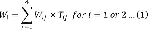
Wijは、各期間Tij(T11~T14,T21~T24)における消費電力Q1,Q2の時間平均である。各パターンPT1,PT2において、各期間Tij(T11~T14,T21~T24)は既知であるものとする。このように定式化される第1の寄与W1及び第2の寄与W2は、通電損失に基づくW12,W,14,W22,W24と、通電損失とスイッチング損失とに基づくW11,W13,W21,W23とで表される。そのため、第1の寄与W1及び第2の寄与W2を用いて、スイッチング素子221において主要な電力損失であるスイッチング損失を推定すること特に重要である。
Wij is the time average of the power consumption Q1, Q2 in each period Tij (T11-T14, T21-T24). In each pattern PT1, PT2, each period Tij (T11-T14, T21-T24) is assumed to be known. The first contribution W1 and the second contribution W2 thus formulated are expressed as W12, W14, W22, and W24 based on the conduction loss, and W11, W13, W21, and W23 based on the conduction loss and the switching loss. Therefore, it is particularly important to estimate the switching loss, which is the main power loss in the
ここで、上記2つの方程式には、2×4種類の合計8つのパラメータWijが含まれている。そのうち、同一の状態に対応する平均的な電力損失は、第1パターンPT1でも第2パターンPT2でも同一であるとして、W1j=W2jと仮定する。これにより、パラメータの数は4つまで減る。また、スイッチング素子221がOFF状態の場合、スイッチング素子221に流れる電流はほぼゼロになることから、OFF期間T13,T23に対応するW13=W23は、ゼロと仮定してもよい。これにより、式(1)で表される連立一次方程式のパラメータは、3つとなる。さらに、第1移行期間T12,T22における消費電力の時間平均W12=W22と、第2移行期間T14,T24における消費電力の時間平均W14=W24は、例えば、現象の可逆性を考慮すれば等しいと仮定しても一定程度妥当である。そのため、W12=W14とすることにより、上記式(1)のパラメータの数は2つとなる。
Here, the above two equations include a total of eight parameters Wij, 2 x 4 types. Among them, the average power loss corresponding to the same state is assumed to be the same in the first pattern PT1 and the second pattern PT2, and W1j = W2j is assumed. This reduces the number of parameters to four. Also, when the switching
スイッチングパターンに含まれるパターンは、そのパターンの数nに応じた連立一次方程式を規定することができる。例えば、上記仮定に基づく近似を用いて、プロセッサ53は、連立一次方程式に含まれるパラメータの数を2つまで減らすことができる。したがって、プロセッサ53は、2つのパターンPT1,PT2におけるそれぞれの寄与W1,W2を用いて、電力損失の内容を推定することができる。特に、移行期間T12,T22,T14,T24における電力損失は、上述したように、通電損失とスイッチング損失とを含む。そのため、移行期間T12,T22,T14,T24における通電損失が、上記連立一次方程式を解くことにより得られたON期間における通電損失を表すW11と等しいと仮定することにより、スイッチング損失が(W12-W11)として得られる。このように、プロセッサ53は、第1の寄与と第2の寄与とを比較することにより、電力損失に含まれるスイッチング損失の寄与や、通電損失の寄与をそれぞれ推定することができる。なお、上記連立一次方程式のパラメータの数に応じてパターンの種類を増やすことにより、近似の少ないより高精度な推定を行うことができる。
The patterns included in the switching pattern can define a simultaneous linear equation according to the number n of the patterns. For example, by using an approximation based on the above assumption, the
ここで、第1移行期間T12,T22及び第2移行期間T14,T24は、スイッチング素子221のスイッチングが高速化するにつれて短くなるとともに、発生頻度が増える。これに伴い、半導体デバイス2の高速化(言い換えれば高周波化)が進むにつれて、スイッチング損失が大きくなる一方で、スイッチングノイズが大きくなるため、スイッチング素子221に印加される電圧や電流を直接測定することにより電力損失(特にスイッチング損失)を推定することが困難となる傾向がある。
Here, the first transition periods T12, T22 and the second transition periods T14, T24 become shorter and occur more frequently as the switching speed of the
そこで、上記のような方法を採用することにより、電力損失を第1の熱流センサ3a及び第2の熱流センサ3bから出力される直流信号(熱起電力)として観測することができる。これにより、スイッチングノイズによってスイッチング素子221の電気的性質を観測することが困難な場合であっても、スイッチング素子221の電力損失の推定を行うことができる。
By adopting the above-mentioned method, the power loss can be observed as a DC signal (thermoelectromotive force) output from the first heat flow sensor 3a and the second
3.推定システム1の別例
さらに推定システム1は、半導体デバイス2による熱の発生状態を模擬する、物理モデルの一例としての参照ユニットを備えていてもよい。図5は、参照ユニットを含む推定システムの構成例を示す図である。図5に示すように、推定システム1は、さらに参照ユニット6と、参照ユニット6からの熱流を測定可能に構成される参照熱流センサ7とを備えていてもよい。参照ユニット6は、半導体デバイス2の熱流に関する挙動を、発熱体等の熱の生成量を制御可能な熱源を用いて再現するように構成される。なお、図5では、説明を簡略化するために、図1で示したガードヒータ25、端子26等の構成は図示されていないが、図5に示される半導体デバイス2も、図1を用いて説明した半導体デバイス2が備える上記種々の構成を備え得る。
3. Another Example of the
図5に示すように、参照ユニット6は、例えば、基板61と、発熱部62を含むと、筐体63と、ヒートシンク64とを備え得る。基板61、筐体63、及びヒートシンク64は、基板21、筐体23、及びヒートシンク24と同様であるため、説明を省略する。
As shown in FIG. 5, the
発熱部62は、半導体デバイス2における素子部22に対応する部材であり、熱を発生させる発熱素子621を備える。発熱素子621は、ヒータ回路または誘導による渦電流が発生する金属板を用いて実装され得る。プロセッサ53は、発熱素子621に入力される電力から、検量線(入力電力に対する熱流センサの出力)を作成する。当該検量線は、例えば、記憶部52等に記憶され得る。プロセッサ53は、例えば、第1の熱流センサ3aにより測定した測定値を検量線に当てはめることにより、半導体デバイス2の実際の損失電力を推定し得る。言い換えれば、推定システム1は、半導体デバイス2を模した物理モデルにおける熱流の測定結果と、第1の熱流センサ3aの測定結果とを比較することにより、電力損失を推定するように構成され得る。
The
参照熱流センサ7は、半導体デバイス2に対する第1の熱流センサ3aと同様に、筐体63(及びヒートシンク64)を介して発熱素子621から生じる熱に基づく熱流を測定するように構成される。参照熱流センサ7は、例えば、第1の熱流センサ3aと同様に構成され得る。
The reference
参照ユニット6は、半導体デバイス2の内部の熱伝導率や体積などを模擬するように設計することが好ましい。さらに、半導体デバイス2が実際に使われる状況において、定常状態(ON期間及びOFF期間)及び過渡状態(第1移行期間及び第2移行期間)のそれぞれにおける、検量線に印加する時間を求めておいてもよい。これにより、損失電力の推定の精度を向上させることができる。さらに、この参照ユニット6を模擬した物理モデルをシミュレーションにおいて設計してもよい。これにより実物の参照ユニット6を設けなくても、第1の熱流センサ3aの測定値に対する損失電力の値の推定制度を向上させることができる。
The
[その他]
上記推定システム1及び推定システム1を用いた推定方法の態様はあくまで一例であり、これに限られない。例えば、上記推定システム1等は、以下のように変更可能である。
[others]
The above-described
スイッチングパターンは、少なくとも2つのパターン(例えば、第1パターンPT1及び第2パターンPT2)を含んでいればよく、3種類以上のスイッチングパターンを含んでいてもよい。また、各パターンは、周期的なものに限られず、非周期的なもの(例えば、ランダムパターン)であってもよい。 The switching pattern may include at least two patterns (e.g., a first pattern PT1 and a second pattern PT2), and may include three or more types of switching patterns. Furthermore, each pattern is not limited to being periodic, and may be non-periodic (e.g., a random pattern).
また、推定システム1は、プロセッサ53等を用いて、半導体デバイス2の温度と、半導体デバイス2の端子26等の温度を計測することにより、パワー半導体からフットプリント等に流れた熱流を推定してもよい。なお、端子26が接続されるすべてのフットプリント等において温度を測定することが好ましいが、少なくとも1点のみにおいて推定することでも精度は向上し得る。
The
このようなスイッチング素子221を含むデバイスは、MOSFETやIGBT等の半導体デバイス2に限られず、任意である。
The device including such a
第1の熱流センサ3aは、基板21又はヒートシンク24に設けられていなくてもよい。例えば、第1の熱流センサ3aは、スイッチング素子221からの熱が優先的に流れる領域であれば、筐体23等に設けられていてもよい。
The first heat flow sensor 3a does not have to be provided on the
上述した実施形態の態様は、プログラムであってもよい。そのプログラムは、少なくとも1つのコンピュータに、推定方法の各ステップを実行させる。 Aspects of the above-described embodiment may be a program. The program causes at least one computer to execute each step of the estimation method.
さらに、次に記載の各態様で提供されてもよい。 Furthermore, it may be provided in the following forms:
(1)抵抗値を変更可能なスイッチング素子を含むデバイスによる電力損失を推定する方法であって、次の各ステップを含み、熱流測定ステップでは、前記デバイスと熱交換するように構成される第1の熱流センサを用いて、規定のスイッチングパターンで前記スイッチング素子の抵抗値を変更される前記デバイスから生じる熱流を測定し、前記スイッチングパターンは、第1パターンと、前記第1パターンと異なる第2パターンとを含み、推定ステップでは、前記熱流の測定結果のうち、前記第1パターンによる前記熱流の寄与である第1の寄与と、前記第2パターンによる前記熱流の寄与である第2の寄与とを比較することにより、前記電力損失を推定する、方法。 (1) A method for estimating power loss due to a device including a switching element whose resistance value can be changed, comprising the following steps: in the heat flow measurement step, a first heat flow sensor configured to exchange heat with the device is used to measure the heat flow generated from the device, the resistance value of which is changed in a specified switching pattern, the switching pattern including a first pattern and a second pattern different from the first pattern; and in the estimation step, the power loss is estimated by comparing, among the heat flow measurement results, a first contribution which is the contribution of the heat flow due to the first pattern and a second contribution which is the contribution of the heat flow due to the second pattern.
(2)上記(1)に記載の方法において、前記第1パターンは、第1周期で前記スイッチング素子の状態が変化するように構成され、前記第2パターンは、前記第1周期より長い第2周期で前記スイッチング素子の状態が変化するように構成される、方法。 (2) The method according to (1) above, wherein the first pattern is configured so that the state of the switching element changes in a first period, and the second pattern is configured so that the state of the switching element changes in a second period that is longer than the first period.
(3)上記(1)または(2)の何れか1つに記載の方法において、駆動ステップでは、前記スイッチングパターンに基づき前記デバイスを駆動させる、方法。 (3) In the method according to any one of (1) or (2) above, in the driving step, the device is driven based on the switching pattern.
(4)上記(3)の何れか1つに記載の方法において、前記駆動ステップでは、前記第1パターンと前記第2パターンの重ね合わせた前記スイッチングパターンを用いて、前記デバイスを駆動させ、前記推定ステップでは、前記測定結果から、前記第1の寄与と前記第2の寄与とを抽出することにより、前記第1の寄与と前記第2の寄与とを比較する、方法。 (4) A method according to any one of the above (3), wherein in the driving step, the device is driven using the switching pattern in which the first pattern and the second pattern are superimposed, and in the estimation step, the first contribution and the second contribution are compared by extracting them from the measurement results.
(5)上記(1)~(4)の何れか1つに記載の方法において、前記デバイスは、さらに基板と、素子部と、筐体とを備え、前記素子部は、前記基板上に形成され、前記スイッチング素子を含み、前記筐体は、前記基板とともに前記素子部を覆うように構成され、さらに第1の配置ステップでは、前記第1の熱流センサを、前記素子部から前記基板を介して熱流を測定するように配置し、前記熱流測定ステップでは、前記第1の熱流センサを用いて、前記素子部から前記第1の熱流センサへの熱流を測定する、方法。 (5) In the method according to any one of (1) to (4) above, the device further comprises a substrate, an element portion, and a housing, the element portion is formed on the substrate and includes the switching element, the housing is configured to cover the element portion together with the substrate, and further, in the first arrangement step, the first heat flow sensor is arranged to measure the heat flow from the element portion through the substrate, and in the heat flow measurement step, the first heat flow sensor is used to measure the heat flow from the element portion to the first heat flow sensor.
(6)上記(5)に記載の方法において、さらに誘導ステップでは、断熱部材又は熱伝導部材を用いて、前記素子部から前記筐体に向かう流出熱を前記第1の熱流センサに誘導し、前記熱流測定ステップでは、前記第1の熱流センサを用いて、誘導された前記流出熱を含む、前記素子部からの熱流を測定する、方法。 (6) The method according to (5) above, further comprising: in the induction step, using a heat insulating member or a heat conducting member, inducing the outflow heat from the element unit toward the housing to the first heat flow sensor; and in the heat flow measurement step, using the first heat flow sensor, measuring the heat flow from the element unit, including the induced outflow heat.
(7)上記(6)に記載の方法において、前記誘導ステップでは、前記素子部を熱伝導部材を用いて覆い、前記熱伝導部材を、前記第1の熱流センサ又は前記基板に接続することにより、当該熱伝導部材を介して前記流出熱を前記第1の熱流センサに誘導する、方法。 (7) A method according to the above (6), in which the induction step includes covering the element portion with a heat conductive member and connecting the heat conductive member to the first heat flow sensor or the substrate, thereby inducing the outflow heat to the first heat flow sensor via the heat conductive member.
(8)上記(6)または(7)に記載の方法において、前記誘導ステップでは、断熱部材を用いて前記素子部を覆うことにより、前記流出熱を前記第1の熱流センサに誘導する、方法。 (8) The method according to (6) or (7) above, wherein in the induction step, the outflow heat is induced to the first heat flow sensor by covering the element portion with a heat insulating material.
(9)上記(5)~(8)の何れか1つに記載の方法において、前記推定ステップでは、さらに、前記デバイスを模した物理モデルにおける熱流の測定結果と、前記第1の熱流センサの測定結果とを比較することにより、前記電力損失を推定する、方法。 (9) A method according to any one of the above (5) to (8), wherein the estimation step further comprises estimating the power loss by comparing the measurement results of the heat flow in a physical model simulating the device with the measurement results of the first heat flow sensor.
(10)上記(5)~(9)の何れか1つに記載の方法において、前記デバイスは、さらに、前記素子部を、他の素子と接続するための端子を備え、さらに第2の配置ステップでは、前記端子に第2の熱流センサを配置し、前記熱流測定ステップでは、前記第1の熱流センサによる前記基板からの熱流の測定結果と前記第2の熱流センサによる前記端子からの熱流の測定結果とに基づき、前記電力損失による電力を推定する、方法。 (10) In the method according to any one of (5) to (9) above, the device further comprises a terminal for connecting the element portion to another element, and in the second placement step, a second heat flow sensor is placed on the terminal, and in the heat flow measurement step, the power due to the power loss is estimated based on the measurement result of the heat flow from the substrate by the first heat flow sensor and the measurement result of the heat flow from the terminal by the second heat flow sensor.
(11)抵抗値を変更可能なスイッチング素子を含むデバイスによる電力損失を推定するためのプログラムであって、コンピュータに、上記(1)~(10)の何れか1つに記載の方法の各ステップを実行させる、プログラム。
もちろん、この限りではない。
(11) A program for estimating power loss caused by a device including a switching element capable of changing a resistance value, the program causing a computer to execute each step of the method described in any one of (1) to (10) above.
Of course, this is not the case.
さらに、上記各態様とは独立して、又は組み合わせて、以下の態様で提供されてもよい。 Furthermore, the following aspects may be provided independently of or in combination with the above aspects:
(項目1)
発熱体と、
前記発熱体と物理的に接続して設けられる熱流センサと、
前記熱流センサにより取得される信号に基づき、前記発熱体における熱損失を推定する制御装置と、
を備える半導体システム。
(その他項目)
・発熱体は、パワー半導体、CPU等の半導体(例えば所定周波数でスイッチングする処理を行う)、DCDCコンバータ、電源等である。
・複数の周波数における熱損失を測定し、その差分にも続いて、スイッチング損失を測定する。
・電圧や電流値を測定し、上記スイッチング損失との差分から漏れ電流を測定する。
・熱流センサと発熱体の間に、ヒートシンク等の低熱抵抗性の材料が設けられる。
・発熱体と熱流センサとの間は、固体物質を介して接続されている。
・発熱体の近傍にヒータが設けられ、発熱体の外面温度と発熱体の近傍空間の温度とが一定となるように制御される。
・発熱体は断熱材で覆われている。
・発熱体は高熱伝導性のケースで覆われ、ケースは熱流センサと熱結合している。
・発熱体から伸びるフットプリントやリード等の肢構造がある場合に、発熱体の温度と肢構造の温度との差分、または肢構造に設けられる熱流センサにより計測される信号を用いて、損失を算出する。
・熱流センサの熱電変換素子は、ワイル磁性体、ワイル半金属、フェリ磁性体等である。これらの素子の厚みは、1マイクロメートル未満である。
(Item 1)
A heating element;
a heat flow sensor provided in physical connection with the heating element;
A control device that estimates a heat loss in the heating element based on a signal acquired by the heat flow sensor;
A semiconductor system comprising:
(Other items)
The heat generating element is a semiconductor such as a power semiconductor, a CPU (for example, performing a switching process at a predetermined frequency), a DCDC converter, a power supply, or the like.
- Measure the thermal losses at multiple frequencies and then measure the difference followed by the switching losses.
・Measure the voltage and current values, and calculate the leakage current from the difference with the above switching loss.
A material with low thermal resistance, such as a heat sink, is provided between the heat flow sensor and the heating element.
The heating element and the heat flow sensor are connected via a solid material.
A heater is provided near the heating element, and the temperature of the outer surface of the heating element and the temperature of the space near the heating element are controlled to be constant.
- The heating element is covered with insulation material.
・The heating element is covered with a highly thermally conductive case, and the case is thermally coupled to the heat flow sensor.
- When there is a limb structure such as a footprint or lead extending from the heating element, the loss is calculated using the difference between the temperature of the heating element and the temperature of the limb structure, or the signal measured by a heat flow sensor installed in the limb structure.
The thermoelectric conversion elements of the heat flow sensor are Weyl magnets, Weyl semimetals, ferrimagnets, etc. The thickness of these elements is less than 1 micrometer.
最後に、本開示に係る種々の実施形態を説明したが、これらは、例として提示したものであり、発明の範囲を限定することは意図していない。当該新規な実施形態は、その他の様々な形態で実施されることが可能であり、発明の要旨を逸脱しない範囲で、種々の省略、置き換え、変更を行うことができる。当該実施形態やその変形は、発明の範囲や要旨に含まれるとともに、特許請求の範囲に記載された発明とその均等の範囲に含まれるものである。 Finally, various embodiments of the present disclosure have been described, but these are presented as examples and are not intended to limit the scope of the invention. The novel embodiments can be embodied in various other forms, and various omissions, substitutions, and modifications can be made without departing from the gist of the invention. The embodiments and modifications thereof are within the scope and gist of the invention, and are included in the scope of the invention and its equivalents as set forth in the claims.
1:推定システム,2:半導体デバイス,21:基板,22:素子部,221:スイッチング素子,23:筐体,24:ヒートシンク,25:ガードヒータ,26:端子,3a:第1の熱流センサ,3b:第2の熱流センサ,4:測定装置,5:端末,50:通信バス,51:通信部,52:記憶部,53:プロセッサ,54:表示部,55:入力部,6:参照ユニット,61:基板,62:発熱部,621:発熱素子,63:筐体,64:ヒートシンク,7:参照熱流センサ,PT1:第1パターン,PT2:第2パターン,T1:第1周期,T11:ON期間,T12:第1移行期間,T13:OFF期間,T14:第2移行期間,T2:第2周期,T21:ON期間,T22:第1移行期間,T23:OFF期間,T24:第2移行期間 1: Estimation system, 2: Semiconductor device, 21: Substrate, 22: Element section, 221: Switching element, 23: Housing, 24: Heat sink, 25: Guard heater, 26: Terminal, 3a: First heat flow sensor, 3b: Second heat flow sensor, 4: Measuring device, 5: Terminal, 50: Communication bus, 51: Communication section, 52: Memory section, 53: Processor, 54: Display section, 55: Input section, 6: Reference unit, 61: substrate, 62: heat generating part, 621: heat generating element, 63: housing, 64: heat sink, 7: reference heat flow sensor, PT1: first pattern, PT2: second pattern, T1: first cycle, T11: ON period, T12: first transition period, T13: OFF period, T14: second transition period, T2: second cycle, T21: ON period, T22: first transition period, T23: OFF period, T24: second transition period
Claims (11)
次の各ステップを含み、
熱流測定ステップでは、前記デバイスと熱交換するように構成される第1の熱流センサを用いて、規定のスイッチングパターンで前記スイッチング素子の抵抗値を変更される前記デバイスから生じる熱流を測定し、
前記スイッチングパターンは、第1パターンと、前記第1パターンと異なる第2パターンとを含み、
推定ステップでは、前記熱流の測定結果のうち、前記第1パターンによる前記熱流の寄与である第1の寄与と、前記第2パターンによる前記熱流の寄与である第2の寄与とを比較することにより、前記電力損失を推定する、方法。 1. A method for estimating power loss through a device including a switching element with a variable resistance, comprising:
It includes the following steps:
In the heat flow measuring step, a first heat flow sensor configured to exchange heat with the device is used to measure a heat flow generated from the device in which the resistance value of the switching element is changed in a prescribed switching pattern;
the switching pattern includes a first pattern and a second pattern different from the first pattern,
A method in which, in the estimation step, the power loss is estimated by comparing a first contribution, which is a contribution of the heat flow due to the first pattern, with a second contribution, which is a contribution of the heat flow due to the second pattern, from the heat flow measurement results.
前記第1パターンは、第1周期で前記スイッチング素子の状態が変化するように構成され、
前記第2パターンは、前記第1周期より長い第2周期で前記スイッチング素子の状態が変化するように構成される、方法。 10. The method of claim 1 ,
The first pattern is configured such that the state of the switching element changes in a first period;
The second pattern is configured such that the switching element changes state over a second period that is longer than the first period.
駆動ステップでは、前記スイッチングパターンに基づき前記デバイスを駆動させる、方法。 The method according to claim 1 or claim 2,
In the driving step, the device is driven based on the switching pattern.
前記駆動ステップでは、前記第1パターンと前記第2パターンの重ね合わせた前記スイッチングパターンを用いて、前記デバイスを駆動させ、
前記推定ステップでは、前記測定結果から、前記第1の寄与と前記第2の寄与とを抽出することにより、前記第1の寄与と前記第2の寄与とを比較する、方法。 The method according to any one of claims 3,
In the driving step, the device is driven using the switching pattern obtained by superposing the first pattern and the second pattern;
A method according to claim 1, wherein the estimating step compares the first contribution with the second contribution by extracting the first contribution and the second contribution from the measurement result.
前記デバイスは、さらに基板と、素子部と、筐体とを備え、
前記素子部は、前記基板上に形成され、前記スイッチング素子を含み、
前記筐体は、前記基板とともに前記素子部を覆うように構成され、
さらに第1の配置ステップでは、前記第1の熱流センサを、前記素子部から前記基板を介して熱流を測定するように配置し、
前記熱流測定ステップでは、前記第1の熱流センサを用いて、前記素子部から前記第1の熱流センサへの熱流を測定する、方法。 The method according to any one of claims 1 to 4,
The device further includes a substrate, an element portion, and a housing.
the element section is formed on the substrate and includes the switching element,
the housing is configured to cover the element portion together with the substrate,
Furthermore, in the first placement step, the first heat flow sensor is placed so as to measure a heat flow from the element portion through the substrate;
The method, wherein the heat flow measuring step uses the first heat flow sensor to measure the heat flow from the element portion to the first heat flow sensor.
さらに誘導ステップでは、断熱部材又は熱伝導部材を用いて、前記素子部から前記筐体に向かう流出熱を前記第1の熱流センサに誘導し、
前記熱流測定ステップでは、前記第1の熱流センサを用いて、誘導された前記流出熱を含む、前記素子部からの熱流を測定する、方法。 6. The method of claim 5,
Furthermore, in the induction step, a heat insulating member or a heat conductive member is used to induce the outflow heat from the element portion toward the housing to the first heat flow sensor,
The method according to claim 1, wherein the heat flow measuring step uses the first heat flow sensor to measure the heat flow from the element portion, including the induced outflow heat.
前記誘導ステップでは、前記素子部を熱伝導部材を用いて覆い、前記熱伝導部材を、前記第1の熱流センサ又は前記基板に接続することにより、当該熱伝導部材を介して前記流出熱を前記第1の熱流センサに誘導する、方法。 7. The method of claim 6,
In the induction step, the element portion is covered with a thermally conductive member, and the thermally conductive member is connected to the first heat flow sensor or the substrate, thereby inducing the outflow heat to the first heat flow sensor via the thermally conductive member.
前記誘導ステップでは、断熱部材を用いて前記素子部を覆うことにより、前記流出熱を前記第1の熱流センサに誘導する、方法。 The method according to claim 6 or 7,
The method according to the present invention, wherein the inducing step includes covering the element portion with a heat insulating material to induce the outflow heat to the first heat flow sensor.
前記推定ステップでは、さらに、前記デバイスを模した物理モデルにおける熱流の測定結果と、前記第1の熱流センサの測定結果とを比較することにより、前記電力損失を推定する、方法。 The method according to any one of claims 5 to 8,
The method further includes, in the estimating step, estimating the power loss by comparing a measurement result of a heat flow in a physical model simulating the device with a measurement result of the first heat flow sensor.
前記デバイスは、さらに、前記素子部を、他の素子と接続するための端子を備え、
さらに第2の配置ステップでは、前記端子に第2の熱流センサを配置し、
前記熱流測定ステップでは、前記第1の熱流センサによる前記基板からの熱流の測定結果と前記第2の熱流センサによる前記端子からの熱流の測定結果とに基づき、前記電力損失による電力を推定する、方法。 The method according to any one of claims 5 to 9,
the device further includes a terminal for connecting the element portion to another element;
Furthermore, in the second arranging step, a second heat flow sensor is arranged on the terminal;
A method in which, in the heat flow measuring step, the power due to the power loss is estimated based on the measurement result of the heat flow from the board by the first heat flow sensor and the measurement result of the heat flow from the terminal by the second heat flow sensor.
コンピュータに、請求項1~請求項10の何れか1つに記載の方法の各ステップを実行させる、プログラム。 A program for estimating power loss caused by a device including a switching element capable of changing a resistance value,
A program causing a computer to execute each step of the method according to any one of claims 1 to 10.
Applications Claiming Priority (2)
| Application Number | Priority Date | Filing Date | Title |
|---|---|---|---|
| JP2023-177245 | 2023-10-13 | ||
| JP2023177245 | 2023-10-13 |
Publications (1)
| Publication Number | Publication Date |
|---|---|
| WO2025079495A1 true WO2025079495A1 (en) | 2025-04-17 |
Family
ID=95395319
Family Applications (1)
| Application Number | Title | Priority Date | Filing Date |
|---|---|---|---|
| PCT/JP2024/035439 Pending WO2025079495A1 (en) | 2023-10-13 | 2024-10-03 | Method and program for estimating power loss by device |
Country Status (1)
| Country | Link |
|---|---|
| WO (1) | WO2025079495A1 (en) |
Citations (4)
| Publication number | Priority date | Publication date | Assignee | Title |
|---|---|---|---|---|
| JP2015114202A (en) * | 2013-12-11 | 2015-06-22 | 新電元工業株式会社 | Temperature detection device and program therefor |
| JP2017003342A (en) * | 2015-06-08 | 2017-01-05 | ルネサスエレクトロニクス株式会社 | Semiconductor integrated circuit device and electronic device |
| JP2018537061A (en) * | 2016-02-03 | 2018-12-13 | ミツビシ・エレクトリック・アールアンドディー・センター・ヨーロッパ・ビーヴィMitsubishi Electric R&D Centre Europe B.V. | Method and device for estimating damage level or life prediction of power semiconductor modules |
| CN113759229A (en) * | 2021-09-13 | 2021-12-07 | 上海交通大学 | Power semiconductor switching loss measurement method and system based on temperature measurement |
-
2024
- 2024-10-03 WO PCT/JP2024/035439 patent/WO2025079495A1/en active Pending
Patent Citations (4)
| Publication number | Priority date | Publication date | Assignee | Title |
|---|---|---|---|---|
| JP2015114202A (en) * | 2013-12-11 | 2015-06-22 | 新電元工業株式会社 | Temperature detection device and program therefor |
| JP2017003342A (en) * | 2015-06-08 | 2017-01-05 | ルネサスエレクトロニクス株式会社 | Semiconductor integrated circuit device and electronic device |
| JP2018537061A (en) * | 2016-02-03 | 2018-12-13 | ミツビシ・エレクトリック・アールアンドディー・センター・ヨーロッパ・ビーヴィMitsubishi Electric R&D Centre Europe B.V. | Method and device for estimating damage level or life prediction of power semiconductor modules |
| CN113759229A (en) * | 2021-09-13 | 2021-12-07 | 上海交通大学 | Power semiconductor switching loss measurement method and system based on temperature measurement |
Similar Documents
| Publication | Publication Date | Title |
|---|---|---|
| Kim | Development of a numerical method for the performance analysis of thermoelectric generators with thermal and electric contact resistance | |
| Gachovska et al. | A real-time thermal model for monitoring of power semiconductor devices | |
| Ali et al. | Lifetime estimation of discrete IGBT devices based on Gaussian process | |
| US9601404B2 (en) | Thermal resistance measuring method and thermal resistance measuring device | |
| Myeong et al. | Analysis of self heating effect in DC/AC mode in multi-channel GAA-field effect transistor | |
| KR102855015B1 (en) | Method for determining characteristic temperatures of electrical or electronic systems | |
| Chen et al. | Fast full-chip parametric thermal analysis based on enhanced physics enforced neural networks | |
| Slawinski et al. | Electrothermal characterization of large-area organic light-emitting diodes employing finite-element simulation | |
| TWI467165B (en) | Measurement method, measurement apparatus, and computer program product | |
| Zhang et al. | Hot-spot aware thermoelectric array based cooling for multicore processors | |
| Francioso et al. | Experimental assessment of thermoelectric generator package properties: simulated results validation and real gradient capabilities | |
| WO2025079495A1 (en) | Method and program for estimating power loss by device | |
| Guralnik et al. | Determination of thermoelectric properties from micro four-point probe measurements | |
| US20250107044A1 (en) | Performance in two-phase cooling systems | |
| Hu et al. | Transient junction temperature estimation of IGBT using improved thermal model | |
| Wan et al. | Combining theory and experiment to determine thermoelectrics of tellurium doped CoSb3 | |
| KR20210114481A (en) | Heater temperature control method, heater and mount | |
| Farjadian et al. | Hybrid electrothermal model for insulator-to-metal transition in VO 2 thin films | |
| JP2024148566A (en) | Apparatus and method for measuring transverse thermoelectric effect | |
| JP5862510B2 (en) | Semiconductor device evaluation system and evaluation method | |
| Ghibaudo et al. | Numerical simulation and analytical modelling of self-heating in FDSOI MOSFETs down to very deep cryogenic temperatures | |
| Górecki et al. | An influence of the selected factors on the transient thermal impedance model of power MOSFET | |
| Jeon et al. | Circuit modeling of the electro-thermal behavior of nanoscale bulk-FinFETs | |
| WO2024253130A1 (en) | Semiconductor module, abnormality determination system, and abnormality determination method | |
| Nakamura et al. | Evaluation of thermal couple impedance model of power modules for accurate die temperature estimation up to 200° C |
Legal Events
| Date | Code | Title | Description |
|---|---|---|---|
| 121 | Ep: the epo has been informed by wipo that ep was designated in this application |
Ref document number: 24877093 Country of ref document: EP Kind code of ref document: A1 |
|
| ENP | Entry into the national phase |
Ref document number: 2025551454 Country of ref document: JP Kind code of ref document: A |
|
| WWE | Wipo information: entry into national phase |
Ref document number: 2025551454 Country of ref document: JP |