WO2024241966A1 - Viewing angle control system and image display device - Google Patents
Viewing angle control system and image display device Download PDFInfo
- Publication number
- WO2024241966A1 WO2024241966A1 PCT/JP2024/017802 JP2024017802W WO2024241966A1 WO 2024241966 A1 WO2024241966 A1 WO 2024241966A1 JP 2024017802 W JP2024017802 W JP 2024017802W WO 2024241966 A1 WO2024241966 A1 WO 2024241966A1
- Authority
- WO
- WIPO (PCT)
- Prior art keywords
- liquid crystal
- optical compensation
- layer
- compensation layer
- crystal compound
- Prior art date
- Legal status (The legal status is an assumption and is not a legal conclusion. Google has not performed a legal analysis and makes no representation as to the accuracy of the status listed.)
- Pending
Links
Images


Classifications
-
- G—PHYSICS
- G02—OPTICS
- G02F—OPTICAL DEVICES OR ARRANGEMENTS FOR THE CONTROL OF LIGHT BY MODIFICATION OF THE OPTICAL PROPERTIES OF THE MEDIA OF THE ELEMENTS INVOLVED THEREIN; NON-LINEAR OPTICS; FREQUENCY-CHANGING OF LIGHT; OPTICAL LOGIC ELEMENTS; OPTICAL ANALOGUE/DIGITAL CONVERTERS
- G02F1/00—Devices or arrangements for the control of the intensity, colour, phase, polarisation or direction of light arriving from an independent light source, e.g. switching, gating or modulating; Non-linear optics
- G02F1/01—Devices or arrangements for the control of the intensity, colour, phase, polarisation or direction of light arriving from an independent light source, e.g. switching, gating or modulating; Non-linear optics for the control of the intensity, phase, polarisation or colour
- G02F1/13—Devices or arrangements for the control of the intensity, colour, phase, polarisation or direction of light arriving from an independent light source, e.g. switching, gating or modulating; Non-linear optics for the control of the intensity, phase, polarisation or colour based on liquid crystals, e.g. single liquid crystal display cells
- G02F1/133—Constructional arrangements; Operation of liquid crystal cells; Circuit arrangements
- G02F1/1333—Constructional arrangements; Manufacturing methods
- G02F1/1335—Structural association of cells with optical devices, e.g. polarisers or reflectors
- G02F1/13363—Birefringent elements, e.g. for optical compensation
-
- G—PHYSICS
- G02—OPTICS
- G02F—OPTICAL DEVICES OR ARRANGEMENTS FOR THE CONTROL OF LIGHT BY MODIFICATION OF THE OPTICAL PROPERTIES OF THE MEDIA OF THE ELEMENTS INVOLVED THEREIN; NON-LINEAR OPTICS; FREQUENCY-CHANGING OF LIGHT; OPTICAL LOGIC ELEMENTS; OPTICAL ANALOGUE/DIGITAL CONVERTERS
- G02F1/00—Devices or arrangements for the control of the intensity, colour, phase, polarisation or direction of light arriving from an independent light source, e.g. switching, gating or modulating; Non-linear optics
- G02F1/01—Devices or arrangements for the control of the intensity, colour, phase, polarisation or direction of light arriving from an independent light source, e.g. switching, gating or modulating; Non-linear optics for the control of the intensity, phase, polarisation or colour
- G02F1/13—Devices or arrangements for the control of the intensity, colour, phase, polarisation or direction of light arriving from an independent light source, e.g. switching, gating or modulating; Non-linear optics for the control of the intensity, phase, polarisation or colour based on liquid crystals, e.g. single liquid crystal display cells
- G02F1/133—Constructional arrangements; Operation of liquid crystal cells; Circuit arrangements
- G02F1/1333—Constructional arrangements; Manufacturing methods
- G02F1/1347—Arrangement of liquid crystal layers or cells in which the final condition of one light beam is achieved by the addition of the effects of two or more layers or cells
Definitions
- the present invention relates to a viewing angle control system and an image display device.
- Image display devices such as liquid crystal display devices and organic electroluminescence (EL) display devices are widely used as displays for car navigation systems, smartphones, notebook computers, and the like. With these displays, while an image can be observed by an observer in a desired direction, there are cases in which control over the viewing angle direction is required, such as when the image is difficult to observe from other directions.
- EL organic electroluminescence
- Patent Document 1 discloses a display device capable of controlling the viewing angle, which includes a first viewing angle control panel having a first liquid crystal layer containing twisted liquid crystal molecules, and a second viewing angle control panel having a second liquid crystal layer containing twisted liquid crystal molecules.
- an object of the present invention is to provide a viewing angle control system that, when applied to a light source, can achieve high brightness in the front direction and low brightness in an oblique direction at a specific azimuth angle.
- Another object of the present invention is to provide an image display device.
- first optical compensation layer is a layer that exhibits the smallest retardation in a direction tilted from the normal direction of the first optical compensation layer when the retardation is measured in a normal direction of the first optical compensation layer and in a direction tilted from the normal direction of the first optical compensation layer
- second optical compensation layer is a layer that has the smallest phase difference in a direction tilted from the normal direction of the second optical compensation layer when the phase difference is measured from the normal direction of the second optical compensation layer and from a direction tilted from the normal direction of the second optical compensation layer.
- the liquid crystal compound is a discotic liquid crystal compound or a rod-shaped liquid crystal compound.
- an angle formed between a projection axis obtained by projecting an optical axis of the liquid crystal compound onto a surface of the first optical compensation layer and an in-plane slow axis of a surface of the liquid crystal layer in the first liquid crystal cell facing the first optical compensation layer is 45 to 135°
- the viewing angle control system according to (2) or (3), wherein an angle between a projection axis obtained by projecting an optical axis of the liquid crystal compound in the second optical compensation layer onto a surface of the second optical compensation layer and an in-plane slow axis on a surface of the liquid crystal layer in the second liquid crystal cell facing the second optical compensation layer is 45 to 135°.
- a third optical compensation layer is further provided between the first liquid crystal cell and the second polarizer, a fourth optical compensation layer is further provided between the second polarizer and the second liquid crystal cell;
- the third optical compensation layer is a layer which, when the retardation is measured in a normal direction of the third optical compensation layer and in a direction inclined from the normal direction of the third optical compensation layer, exhibits the smallest retardation in a direction inclined from the normal direction of the third optical compensation layer;
- the viewing angle control system according to any one of (1) to (4), wherein the fourth optical compensation layer is a layer that has the smallest retardation in a direction tilted from the normal direction of the fourth optical compensation layer when the retardation is measured in a normal direction of the fourth optical compensation layer and in a direction tilted from the normal direction of the fourth optical compensation layer.
- An image display device comprising an image display element and the viewing angle control system according to any one of (1) to (5).
- an image display device can be provided.
- FIG. 1 is a schematic cross-sectional view of a first embodiment of a viewing angle control system of the present invention.
- 2 is a diagram showing the relationship between the transmission axis of the first polarizer, the transmission axis of the second polarizer, and the transmission axis of the third polarizer in the viewing angle control system shown in FIG. 1 when observed from the direction of the white arrow in FIG. 1.
- 3 is a diagram showing the relationship between the transmission axis of the first polarizer, the rod-shaped liquid crystal compound contained in the liquid crystal layer in the first liquid crystal cell, and the transmission axis of the second polarizer in the viewing angle control system shown in FIG. 1 when observed from the direction of the white arrow in FIG.
- FIG. 4 is a diagram showing the relationship between the transmission axis of the second polarizer, the rod-shaped liquid crystal compound contained in the liquid crystal layer in the second liquid crystal cell, and the transmission axis of the third polarizer in the viewing angle control system shown in FIG. 1 when observed from the direction of the white arrow in FIG.
- FIG. 5 is a diagram showing the alignment state of rod-shaped liquid crystal compounds contained in the liquid crystal layer in the second liquid crystal cell.
- FIG. 6 is a diagram showing the alignment state of rod-shaped liquid crystal compounds contained in the liquid crystal layer in the second liquid crystal cell.
- FIG. 7 is a diagram showing the results when the azimuth angle and polar angle are changed from the direction of the white arrow shown in FIG. FIG.
- FIG. 8 is a diagram showing the alignment state of rod-shaped liquid crystal compounds contained in the liquid crystal layer in the first liquid crystal cell.
- FIG. 9 is a diagram showing the results when the azimuth angle and polar angle are changed from the direction of the white arrow shown in FIG.
- FIG. 10 is a diagram showing an overlapping area between the areas enclosed by thick lines in FIG. 7 and FIG.
- FIG. 11 is a diagram showing the configurations of the second liquid crystal cell and the second optical compensation layer.
- Figure 12 shows the relationship between the projected axis obtained by projecting the optical axis of the discotic liquid crystal compound onto the surface of the second optical compensation layer, and the in-plane slow axis on the surface of the liquid crystal layer in the second liquid crystal cell on the second optical compensation layer side.
- FIG. 13 is a diagram showing a configuration of the second optical compensation layer in the modified example of the first embodiment of the viewing angle control system of the present invention.
- Figure 14 shows the relationship between the projected axis obtained by projecting the optical axis of the discotic liquid crystal compound onto the surface of the second optical compensation layer, and the in-plane slow axis on the surface of the liquid crystal layer in the second liquid crystal cell on the second optical compensation layer side.
- FIG. 15 is a schematic cross-sectional view of a second embodiment of the viewing angle control system of the present invention.
- parallel and orthogonal do not mean parallel and orthogonal in the strict sense, but rather mean a range of parallel ⁇ 5° (a range of ⁇ 5° from parallel) and a range of orthogonal ⁇ 5° (a range of ⁇ 5° from orthogonal), respectively.
- absorption axis refers to the polarization direction in which the absorbance is maximum in the plane when linearly polarized light is incident.
- Transmission axis refers to the direction that forms an angle of 90° with the absorption axis in the plane.
- in-plane slow axis refers to the direction in which the refractive index is maximum in the plane.
- Re( ⁇ ) and Rth( ⁇ ) respectively represent the in-plane retardation and the thickness retardation at a wavelength ⁇ .
- the wavelength ⁇ is 550 nm.
- Re( ⁇ ) and Rth( ⁇ ) are values measured at a wavelength ⁇ using an AxoScan (manufactured by Axometrics).
- AxoScan manufactured by Axometrics.
- Re( ⁇ ) R0( ⁇ )
- NAR-4T Abbe refractometer
- the measurement can be performed using a multi-wavelength Abbe refractometer DR-M2 (manufactured by Atago Co., Ltd.) in combination with an interference filter.
- values in the Polymer Handbook JOHN WILEY & SONS, INC.
- catalogs of various optical films can be used.
- Examples of average refractive index values of major optical films are as follows: cellulose acylate (1.48), cycloolefin polymer (1.52), polycarbonate (1.59), polymethyl methacrylate (1.49), and polystyrene (1.59).
- each component may be a single substance corresponding to the component, or two or more substances may be used in combination.
- the content of that component refers to the total content of the substances used in combination, unless otherwise specified.
- (meth)acrylate is a notation that represents “acrylate” or “methacrylate”
- (meth)acrylic is a notation that represents “acrylic” or “methacrylic”
- (meth)acryloyl is a notation that represents "acryloyl” or “methacryloyl”.
- FIG. 1 shows a first embodiment of a viewing angle control system according to the present invention.
- 1 includes, in this order, a first polarizer 10, a first optical compensation layer 12, a first liquid crystal cell 14, a second polarizer 16, a second liquid crystal cell 18, a second optical compensation layer 20, and a third polarizer 22.
- a viewing angle control system 100A is disposed on a light source and a voltage is applied to each of the first liquid crystal cell 14 and the second liquid crystal cell 18 to turn them on, it is possible to realize high luminance in the front direction and low luminance in an oblique direction at a specific azimuth angle.
- the viewing angle is controlled by the first polarizer 10, the second polarizer 16, the third polarizer 22, the first liquid crystal cell 14 and the second liquid crystal cell 18 will be described below.
- Fig. 2 is a diagram showing the relationship between the transmission axis of the first polarizer 10, the transmission axis of the second polarizer 16, and the transmission axis of the third polarizer 22 in the viewing angle control system 100A shown in Fig. 1 when observed from the direction of the white arrow in Fig. 1.
- the arrows in the first polarizer 10, the second polarizer 16, and the third polarizer 22 in Fig. 2 represent the transmission axes.
- the angle between the transmission axis of the first polarizer 10 and the transmission axis of the second polarizer 16 is 90°. Note that the present invention is not limited to the embodiment shown in Fig.
- the angle between the transmission axis of the first polarizer and the transmission axis of the second polarizer is preferably in the range of 85 to 95°, and more preferably in the range of 88 to 92°.
- the transmission axis of the first polarizer and the transmission axis of the second polarizer are perpendicular to each other.
- the angle between the transmission axis of the second polarizer 16 and the transmission axis of the third polarizer 22 is 90°. Note that the present invention is not limited to the embodiment shown in Fig.
- the angle between the transmission axis of the second polarizer and the transmission axis of the third polarizer is preferably in the range of 85 to 95°, and more preferably in the range of 88 to 92°. In other words, it is preferable that the transmission axis of the second polarizer and the transmission axis of the third polarizer are perpendicular to each other.
- Fig. 3 is a diagram showing the relationship between the transmission axis of the first polarizer 10, the rod-like liquid crystal compound contained in the liquid crystal layer in the first liquid crystal cell 14, and the transmission axis of the second polarizer 16 in the viewing angle control system 100A shown in Fig. 1 when observed from the direction of the white arrow in Fig. 1.
- the arrows in the first polarizer 10 and the second polarizer 16 in Fig. 3 represent the transmission axes. 3 shows the initial alignment state of the liquid crystal compound at the off-state where no voltage is applied to the liquid crystal layer in the first liquid crystal cell 14.
- the first liquid crystal cell 14 is a so-called TN mode liquid crystal cell.
- the angle between the transmission axis of the first polarizer 10 and the transmission axis of the second polarizer 16 is 90°.
- the rod-shaped liquid crystal compounds contained in the liquid crystal layer in the first liquid crystal cell 14 are twisted. More specifically, when the rod-shaped liquid crystal compound LC2 located on the second polarizer 16 side of the liquid crystal layer in the first liquid crystal cell 14 is used as a reference, the rod-shaped liquid crystal compounds are twisted (torsional) in a clockwise direction.
- the angle between the long axis direction of the rod-shaped liquid crystal compound LC1 contained in the liquid crystal layer in the first liquid crystal cell 14 and located on the first polarizer 10 side and the transmission axis of the first polarizer 10 is 0°.
- the present invention is not limited to the embodiment of Fig. 3, and the angle between the long axis direction of the rod-shaped liquid crystal compound contained in the liquid crystal layer in the first liquid crystal cell and located on the first polarizer side and the transmission axis of the first polarizer is preferably in the range of 0 to 5°, more preferably in the range of 0 to 2°.
- the long axis direction of the rod-shaped liquid crystal compound contained in the liquid crystal layer in the first liquid crystal cell and located on the first polarizer side and the transmission axis of the first polarizer are parallel to each other.
- the angle between the long axis direction of the rod-shaped liquid crystal compound LC2 contained in the liquid crystal layer in the first liquid crystal cell 14 and located on the second polarizer 16 side and the transmission axis of the second polarizer 16 is 0°. Note that the present invention is not limited to the embodiment of Fig.
- the angle between the long axis direction of the rod-shaped liquid crystal compound contained in the liquid crystal layer in the first liquid crystal cell and located on the second polarizer side and the transmission axis of the second polarizer is preferably in the range of 0 to 5°, more preferably in the range of 0 to 2°.
- the long axis direction of the rod-shaped liquid crystal compound contained in the liquid crystal layer in the first liquid crystal cell and located on the second polarizer side and the transmission axis of the second polarizer are parallel to each other.
- the rod-shaped liquid crystal compound is twisted in orientation with a twist angle of 90° in Fig. 3.
- the present invention is not limited to the embodiment shown in Fig.
- the twist angle is preferably in the range of 85 to 95°, and more preferably in the range of 88 to 92°.
- the rod-shaped liquid crystal compound is twisted clockwise, but may be twisted counterclockwise.
- the liquid crystal compound contained in the liquid crystal layer in the first liquid crystal cell may have a predetermined pretilt angle.
- Fig. 4 is a diagram showing the relationship between the transmission axis of the second polarizer 16, the rod-like liquid crystal compound contained in the liquid crystal layer in the second liquid crystal cell 18, and the transmission axis of the third polarizer 22 in the viewing angle control system 100A shown in Fig. 1 when observed from the direction of the white arrow in Fig. 1.
- the arrows in the second polarizer 16 and the third polarizer 22 in Fig. 4 represent the transmission axes. 4 shows the initial alignment state of the liquid crystal compound at the off-state where no voltage is applied to the liquid crystal layer in the second liquid crystal cell 18.
- the second liquid crystal cell 18 is a so-called TN mode liquid crystal cell.
- the angle between the transmission axis of the second polarizer 16 and the transmission axis of the third polarizer 22 is 90°.
- the rod-shaped liquid crystal compounds contained in the liquid crystal layer in the second liquid crystal cell 18 are twisted. More specifically, when the rod-shaped liquid crystal compound LC4 located on the third polarizer 22 side of the liquid crystal layer in the second liquid crystal cell 18 is used as a reference, the rod-shaped liquid crystal compounds are twisted in a clockwise direction.
- the angle between the long axis direction of the rod-shaped liquid crystal compound LC3 contained in the liquid crystal layer in the second liquid crystal cell 18 and located on the second polarizer 16 side and the transmission axis of the second polarizer 16 is 0°.
- the present invention is not limited to the embodiment of Fig. 4, and the angle between the long axis direction of the rod-shaped liquid crystal compound contained in the liquid crystal layer in the second liquid crystal cell and located on the second polarizer side and the transmission axis of the second polarizer is preferably in the range of 0 to 5°, more preferably in the range of 0 to 2°.
- the long axis direction of the rod-shaped liquid crystal compound contained in the liquid crystal layer in the second liquid crystal cell and located on the second polarizer side and the transmission axis of the second polarizer are parallel to each other.
- the angle between the long axis direction of the rod-shaped liquid crystal compound LC4 contained in the liquid crystal layer in the second liquid crystal cell 18 and located on the third polarizer 22 side and the transmission axis of the third polarizer 22 is 0°. Note that the present invention is not limited to the embodiment of Fig.
- the angle between the long axis direction of the rod-shaped liquid crystal compound contained in the liquid crystal layer in the second liquid crystal cell and located on the third polarizer side and the transmission axis of the third polarizer is preferably in the range of 0 to 5°, more preferably in the range of 0 to 2°. It is preferable that the long axis direction of the rod-shaped liquid crystal compound contained in the liquid crystal layer in the first liquid crystal cell and located on the third polarizer side and the transmission axis of the third polarizer are parallel to each other. As described above, the rod-shaped liquid crystal compound is twisted in the orientation shown in Fig. 4, and the twist angle is 90°. However, the present invention is not limited to the embodiment shown in Fig.
- the twist angle is preferably in the range of 85 to 95°, and more preferably in the range of 88 to 92°.
- the rod-shaped liquid crystal compound is twisted clockwise, but may be twisted counterclockwise.
- the liquid crystal compound contained in the liquid crystal layer in the second liquid crystal cell may have a predetermined pretilt angle.
- FIGS 5 and 6 are diagrams showing the alignment state of the rod-shaped liquid crystal compounds contained in the liquid crystal layer 24 in the second liquid crystal cell 18.
- a rod-shaped liquid crystal compound LC10 contained in the liquid crystal layer 24 in the second liquid crystal cell 18 and located on the second polarizer 16 side a rod-shaped liquid crystal compound LC11 contained in the liquid crystal layer 24 in the second liquid crystal cell 18 and located on the third polarizer 22 side
- the second liquid crystal cell 18 has a liquid crystal layer 24 sandwiched between two substrates (a first substrate 26 and a second substrate 28).
- the configuration of the second liquid crystal cell 18 will be described in detail later.
- FIG. 5 shows the initial alignment state of the rod-shaped liquid crystal compound LC in the second liquid crystal cell 18 in the off state where no voltage is applied to the liquid crystal layer 24 .
- the rod-shaped liquid crystal compounds (rod-shaped liquid crystal compounds LC10 to LC12) are horizontally aligned.
- the twist angle of the rod-shaped liquid crystal compounds is 90°.
- the rod-shaped liquid crystal compounds LC10 and LC11 are horizontally aligned, but may have a tilt angle.
- Fig. 6 shows the alignment state of the rod-shaped liquid crystal compound LC when a voltage is applied to the liquid crystal layer 24 in the second liquid crystal cell 18.
- Fig. 6 shows the alignment state when a voltage of about half the maximum voltage (e.g., about 2.5 V) is applied.
- the rod-shaped liquid crystal compound is tilted.
- the rod-shaped liquid crystal compound LC12 located at the middle position of the liquid crystal layer 24 is easily tilted by the influence of the voltage. At that time, the azimuth angle of the long axis direction of the rod-shaped liquid crystal compound LC12 is hardly changed.
- the rod-like liquid crystal compound LC10 located on the second polarizer 16 side and the rod-like liquid crystal compound LC11 located on the third polarizer 22 side are difficult to tilt.
- the direction to the right side of the paper in Figure 7 corresponds to the tip side of the X-axis arrow in Figure 6, the direction to the left side of the paper in Figure 7 corresponds to the rear end side of the X-axis arrow in Figure 6, the direction to the bottom of the paper in Figure 7 corresponds to the front side of the paper in Figure 6, and the direction to the top of the paper in Figure 7 corresponds to the back side of the paper in Figure 6.
- the centers of the concentric circles correspond to the normal direction of the second liquid crystal cell 18, and the concentric circles of different sizes have inclination angles (polar angles) relative to the normal direction of 20°, 40°, 60°, and 80°, respectively.
- Figure 7 shows the results when a light source is placed on the side of the second polarizer 16 opposite the second liquid crystal cell 18, in a configuration including the second polarizer 16, the second liquid crystal cell 18, and the third polarizer 22, and the azimuth angle and polar angle are changed and viewed from the third polarizer 22 side.
- the black circle in Figure 7 corresponds to the position of the result viewed from a polar angle of 40° along the azimuth angle toward the tip side in the X-axis direction.
- the liquid crystal layer 24 functions as a retardation layer like a ⁇ /2 plate due to the influence of the orientation of the rod-like liquid crystal compound contained in the liquid crystal layer 24 in the second liquid crystal cell 18, and the direction of the polarized light transmitted through the second polarizer 16 is rotated to be parallel to the transmission axis direction of the third polarizer 22, and the light is transmitted through the third polarizer 22 and is visible.
- Fig. 8 is a diagram showing the alignment state of rod-shaped liquid crystal compounds contained in the liquid crystal layer 30 in the first liquid crystal cell 14.
- the first liquid crystal cell 14 has a liquid crystal layer 30 sandwiched between two substrates (a first substrate 32 and a second substrate 34). The configuration of the first liquid crystal cell 14 will be described in detail later. Fig.
- FIG. 8 shows the alignment state of the rod-shaped liquid crystal compound LC when a voltage is applied to the liquid crystal layer 30 in the first liquid crystal cell 14.
- Fig. 8 shows the alignment state when a voltage of about half the maximum voltage (e.g., about 2.5 V) is applied.
- the rod-shaped liquid crystal compound is tilted.
- the rod-shaped liquid crystal compound LC22 located at the middle position of the liquid crystal layer 30 is easily tilted by the influence of the voltage. At that time, the azimuth angle of the long axis direction of the rod-shaped liquid crystal compound LC22 is hardly changed.
- the rod-like liquid crystal compound LC20 located on the first polarizer 10 side and the rod-like liquid crystal compound LC21 located on the second polarizer 16 side are difficult to tilt.
- the direction to the right side of the paper in Figure 9 corresponds to the tip side of the X-axis arrow in Figure 8
- the direction to the left side of the paper in Figure 9 corresponds to the rear end side of the X-axis arrow in Figure 8
- the direction to the bottom of the paper in Figure 9 corresponds to the front side of the paper in Figure 8
- the direction to the top of the paper in Figure 9 corresponds to the back side of the paper in Figure 8.
- the centers of the concentric circles correspond to the normal direction of the first liquid crystal cell 14, and the concentric circles of different sizes correspond to inclination angles (polar angles) of 20°, 40°, 60°, and 80° with respect to the normal direction.
- Figure 9 shows the results of viewing an image having a configuration of a first polarizer 10, a first liquid crystal cell 14, and a second polarizer 16, with a light source disposed on the side of the first polarizer 10 opposite the first liquid crystal cell 14, and the azimuth angle and polar angle changed from the second polarizer 16 side.
- a light source arranged on the opposite side of the first polarizer 10 from the first liquid crystal cell 14 was visible, while in other areas, light from the light source was difficult to see or was not visible at all.
- light can be transmitted in a specific direction by applying a voltage to the liquid crystal layer 30 of the first liquid crystal cell 14.
- the configurations of the first polarizer 10, the first liquid crystal cell 14, and the second polarizer 16, and the configurations of the second polarizer 16, the second liquid crystal cell 18, and the third polarizer 22 can each control the viewing angle. Therefore, when the above two configurations are combined in the thickness direction and both the first liquid crystal cell 14 and the second liquid crystal cell 18 are turned on, the light from the light source can be seen in the area where the areas surrounded by the thick lines in Figures 7 and 9 overlap, as shown in Figure 10.
- Such a mechanism is also disclosed in the above-mentioned Patent Document 1.
- the rod-shaped liquid crystal compound LC10 and the rod-shaped liquid crystal compound LC11 are unlikely to be tilted like the rod-shaped liquid crystal compound LC12. If such rod-shaped liquid crystal compound LC10 and the rod-shaped liquid crystal compound LC11 are contained, the function of the liquid crystal layer 24 as a retardation layer is reduced, which may cause light leakage in a viewing angle control system.
- the present inventors have found that the influence of the rod-shaped liquid crystal compound LC11 is particularly large.
- the second optical compensation layer 20 shown in FIG. 1 is provided to eliminate the light leakage caused by the rod-like liquid crystal compound LC11.
- the second optical compensation layer 20 corresponds to a layer that has the smallest retardation in a direction tilted from the normal direction when the retardation is measured in the normal direction of the second optical compensation layer and in a direction tilted from the normal direction.
- Fig. 11 shows the configurations of the second liquid crystal cell 18 and the second optical compensation layer 20.
- the second liquid crystal cell 18 is in the power-on state shown in Fig. 6, and as described above, when the power is on in the second liquid crystal cell 18, the rod-shaped liquid crystal compound LC11 is unlikely to be tilted.
- the optical effect of the rod-shaped liquid crystal compound LC11 is eliminated by disposing the second optical compensation layer 20 which is a layer in which the tilted alignment of the discotic liquid crystal compound DL1 is fixed.
- the disc surface of the discotic liquid crystal compound DL1 is parallel to the depth direction of the page, and the projection axis of the optical axis of the discotic liquid crystal compound DL1 projected onto the surface (principal surface) of the second optical compensation layer 20 is shown as a black arrow in FIG. 12.
- the optical axis of the discotic liquid crystal compound DL1 is an axis along the normal direction of the disc surface of the discotic liquid crystal compound DL1.
- the surface of the second optical compensation layer 20 corresponds to one of the two principal surfaces perpendicular to the thickness direction of the second optical compensation layer 20.
- the principal surface means the surface of the second optical compensation layer 20 with the largest area.
- the in-plane slow axis on the surface of the liquid crystal layer 24 on the second optical compensation layer 20 side in the second liquid crystal cell 18 is indicated by a white arrow.
- the in-plane slow axis also corresponds to the projection axis of the optical axis of the rod-shaped liquid crystal compound LC11 (the long axis of the rod-shaped liquid crystal compound LC11) located on the second optical compensation layer 20 side of the liquid crystal layer 24 projected onto the surface of the second optical compensation layer 20.
- the angle between the black arrow and the white arrow is 0°.
- the angle between the projection axis formed by projecting the optical axis of the discotic liquid crystal compound DL1 on the surface of the second optical compensation layer 20 in the second optical compensation layer 20 and the in-plane slow axis on the surface of the liquid crystal layer 24 on the second optical compensation layer 20 side in the second liquid crystal cell 18 is 0°.
- the angle between the projection axis formed by projecting the optical axis of the liquid crystal compound on the surface of the second optical compensation layer in the second optical compensation layer and the in-plane slow axis on the surface of the liquid crystal layer on the second optical compensation layer side in the second liquid crystal cell is preferably 0 to 45°, more preferably 0 to 20°, still more preferably 0 to 5°, and particularly preferably 0 to 2°.
- the projection axis formed by projecting the optical axis of the liquid crystal compound on the surface of the second optical compensation layer in the second optical compensation layer and the in-plane slow axis on the surface of the liquid crystal layer on the second optical compensation layer side in the second liquid crystal cell are parallel.
- the angle between the discotic plane of the discotic liquid crystal compound DL1 in the second optical compensation layer 20 and the surface of the second optical compensation layer 20 is not particularly limited, but is preferably from 10 to 45°, and more preferably from 15 to 35°.
- the angle between the azimuth angle of the optical axis (long axis) of the rod-shaped liquid crystal compound LC11 located on the surface of the second optical compensation layer 20 side of the liquid crystal layer 24 in the second liquid crystal cell 18 from one end opposite to the second optical compensation layer 20 side toward one end on the second optical compensation layer 20 side and the azimuth angle of the optical axis of the discotic liquid crystal compound DL1 from one end on the second liquid crystal cell 18 side toward one end opposite to the second liquid crystal cell 18 side is 0°.
- the angle between the azimuth angle of the optical axis (long axis) of the rod-shaped liquid crystal compound located on the surface of the second optical compensation layer side of the liquid crystal layer in the second liquid crystal cell from one end opposite to the second optical compensation layer side toward one end on the second optical compensation layer side and the azimuth angle of the optical axis of the discotic liquid crystal compound from one end on the second liquid crystal cell side toward one end opposite to the second liquid crystal cell side is preferably 0 to 45°, more preferably 0 to 20°, still more preferably 0 to 5°, and particularly preferably 0 to 2°.
- the azimuth angle of the optical axis (long axis) of the rod-shaped liquid crystal compound located on the surface of the liquid crystal layer in the second liquid crystal cell facing the second optical compensation layer, from one end opposite the second optical compensation layer side to one end on the second optical compensation layer side, and the azimuth angle of the optical axis of the discotic liquid crystal compound, from one end on the second liquid crystal cell side to one end opposite the second liquid crystal cell side, are parallel.
- the azimuth angle mentioned above means the azimuth angle on the xy plane in FIG.
- the second optical compensation layer 20 contains the discotic liquid crystal compound DL1, but the second optical compensation layer may contain a rod-shaped liquid crystal compound.
- the angle between the projection axis obtained by projecting the optical axis of the rod-shaped liquid crystal compound onto the surface of the second optical compensation layer and the in-plane slow axis on the surface of the liquid crystal layer on the second optical compensation layer side in the second liquid crystal cell is preferably 0 to 45°, more preferably 0 to 20°, even more preferably 0 to 5°, and particularly preferably 0 to 2°.
- the angle between the major axis of the rod-like liquid crystal compound and the surface of the second optical compensation layer is not particularly limited, but is preferably 10 to 45°, more preferably 15 to 35°.
- the angle between the azimuth angle from one end of the optical axis (long axis) of the rod-shaped liquid crystal compound located on the surface of the liquid crystal layer in the second liquid crystal cell facing the second optical compensation layer side toward one end of the second optical compensation layer side, and the azimuth angle from one end of the optical axis of the rod-shaped liquid crystal compound contained in the second optical compensation layer toward one end of the optical axis facing the second liquid crystal cell side toward one end of the optical axis facing the second liquid crystal cell side is preferably 135 to 225°, more preferably 160 to 200°, and even more preferably 175 to 185°.
- the rod-shaped liquid crystal compound LC20 and the rod-shaped liquid crystal compound LC21 are unlikely to be tilted like the rod-shaped liquid crystal compound LC22. If such rod-shaped liquid crystal compounds LC20 and LC21 are contained, the function of the liquid crystal layer 30 as a retardation layer is reduced, which may cause light leakage in a viewing angle control system.
- the present inventors have found that the influence of the rod-shaped liquid crystal compound LC20 is particularly large.
- the first optical compensation layer 12 shown in FIG. 1 is provided to eliminate the light leakage caused by the rod-like liquid crystal compound LC20.
- the first optical compensation layer 12 is a layer formed by fixing an inclined discotic liquid crystal compound, and eliminates the optical influence of the rod-shaped liquid crystal compound LC20.
- the angle between the projection axis obtained by projecting the optical axis of the discotic liquid crystal compound contained in the first optical compensation layer 12 onto the surface (principal surface) of the first optical compensation layer 12 and the in-plane slow axis on the surface of the liquid crystal layer in the first liquid crystal cell 14 facing the first optical compensation layer 12 is 0°.
- the surface of the first optical compensation layer 12 corresponds to one of two principal surfaces perpendicular to the thickness direction of the first optical compensation layer 12.
- the principal surface means the surface of the first optical compensation layer 12 that has the largest area.
- the angle between the projection axis obtained by projecting the optical axis of the liquid crystal compound in the first optical compensation layer onto the surface of the first optical compensation layer and the in-plane slow axis on the surface of the liquid crystal layer in the first liquid crystal cell on the first optical compensation layer side is preferably 0 to 45°, more preferably 0 to 20°, still more preferably 0 to 5°, and particularly preferably 0 to 2°.
- the projection axis obtained by projecting the optical axis of the discotic liquid crystal compound contained in the first optical compensation layer onto the surface of the first optical compensation layer and the in-plane slow axis on the surface of the liquid crystal layer in the first liquid crystal cell on the first optical compensation layer side are parallel to each other.
- the angle between the discotic plane of the discotic liquid crystal compound in the first optical compensation layer and the surface of the first optical compensation layer is not particularly limited, but is preferably from 10 to 45°, more preferably from 15 to 35°.
- the angle between the azimuth angle of the optical axis (long axis) of the rod-shaped liquid crystal compound LC20 located on the surface of the first optical compensation layer 10 side of the liquid crystal layer 30 in the first liquid crystal cell 14 from one end on the first optical compensation layer 10 side to one end on the opposite side to the first optical compensation layer 10 side and the azimuth angle of the optical axis of the discotic liquid crystal compound contained in the first optical compensation layer 12 from one end on the opposite side to the first liquid crystal cell 14 side to one end on the first liquid crystal cell 14 side is 0°.
- the angle between the azimuth angle of the optical axis (long axis) of the rod-shaped liquid crystal compound located on the surface of the first optical compensation layer side of the liquid crystal layer in the first liquid crystal cell from one end on the first optical compensation layer side to one end on the opposite side to the first optical compensation layer side and the azimuth angle of the optical axis of the discotic liquid crystal compound contained in the first optical compensation layer from one end on the opposite side to the first liquid crystal cell side to one end on the first liquid crystal cell side is preferably 0 to 45°, more preferably 0 to 20°, even more preferably 0 to 5°, and particularly preferably 0 to 2°.
- the azimuth angle of the optical axis (long axis) of the rod-shaped liquid crystal compound located on the surface of the liquid crystal layer on the first optical compensation layer side in the first liquid crystal cell from one end on the first optical compensation layer side to one end on the opposite side to the first optical compensation layer side, and the azimuth angle of the optical axis of the discotic liquid crystal compound contained in the first optical compensation layer from one end on the opposite side to the first liquid crystal cell side to one end on the first liquid crystal cell side are parallel.
- the first optical compensation layer contains a discotic liquid crystal compound, but the first optical compensation layer may contain a rod-shaped liquid crystal compound.
- the angle between the projection axis obtained by projecting the optical axis of the rod-shaped liquid crystal compound onto the surface of the first optical compensation layer and the in-plane slow axis on the surface of the liquid crystal layer on the first optical compensation layer side in the first liquid crystal cell is within the above range.
- the angle between the major axis of the rod-like liquid crystal compound and the surface of the first optical compensation layer is not particularly limited, but is preferably 10 to 45°, more preferably 15 to 35°.
- the angle between the azimuth angle from one end of the optical axis (long axis) of the rod-shaped liquid crystal compound located on the surface of the liquid crystal layer in the first liquid crystal cell on the first optical compensation layer side toward one end opposite the first optical compensation layer side, and the azimuth angle from one end of the optical axis of the rod-shaped liquid crystal compound contained in the first optical compensation layer opposite the first liquid crystal cell side toward one end on the first liquid crystal cell side is preferably 135 to 225°, more preferably 160 to 200°, and even more preferably 175 to 185°.
- a modified example of the first embodiment of the viewing angle control system of the present invention may be an embodiment in which the optical axes of the liquid crystal compounds contained in the first optical compensation layer and/or the second optical compensation layer are different from each other. More specifically, in FIG. 13, except that the second optical compensation layer 20A is used, this corresponds to an aspect having the configuration of the viewing angle control system described in the above-mentioned first embodiment.
- the second optical compensation layer 20A is a layer formed by fixing the inclined discotic liquid crystal compound DL2, and the direction of the optical axis of the discotic liquid crystal compound is different from that of the second optical compensation layer 20 shown in FIG. In the configuration shown in Fig.
- the projection axis obtained by projecting the optical axis of the discotic liquid crystal compound DL2 onto the surface (principal surface) of the second optical compensation layer 20A is shown as a black arrow in Fig. 14.
- the optical axis of the discotic liquid crystal compound DL2 is an axis along the normal direction of the discotic surface of the discotic liquid crystal compound DL2.
- the in-plane slow axis of the liquid crystal layer 24 in the second liquid crystal cell 18 on the surface facing the second optical compensation layer 20A is indicated by a white arrow in FIG. 14, the angle between the black arrow and the white arrow is 90°.
- the angle between the projection axis obtained by projecting the optical axis of the discotic liquid crystal compound DL1 in the second optical compensation layer 20A onto the surface of the second optical compensation layer 20A and the in-plane slow axis of the surface of the liquid crystal layer 24 in the second liquid crystal cell 18 on the second optical compensation layer 20A side is 90°.
- the inventors have found that the configuration shown in FIG. 13 suppresses light leakage more effectively than the configuration shown in FIG. 10, and as a result, achieves a lower brightness in oblique directions at a particular azimuth angle.
- the present invention is not limited to this embodiment, and the angle between the projection axis formed by projecting the optical axis of the liquid crystal compound in the second optical compensation layer onto the surface of the second optical compensation layer and the in-plane slow axis on the surface of the liquid crystal layer in the second liquid crystal cell facing the second optical compensation layer is preferably 45 to 135°, more preferably 70 to 110°, and even more preferably 85 to 95°.
- the angle between the discotic plane of the discotic liquid crystal compound DL2 in the second optical compensation layer 20A and the surface of the second optical compensation layer 20 is not particularly limited, but is preferably from 10 to 45°, and more preferably from 15 to 35°.
- the rod-shaped liquid crystal compound located on the second optical compensation layer 20A side of the liquid crystal layer 24 in the second liquid crystal cell 18 is used as a reference, the rod-shaped liquid crystal compound is twisted in a clockwise direction.
- the azimuth angle of the optical axis of the discotic liquid crystal compound DL1 from one end on the second liquid crystal cell 18 side to one end on the opposite side to the second liquid crystal cell 18 side is used as a reference, the azimuth angle of the optical axis (long axis) of the rod-shaped liquid crystal compound LC11 located on the surface of the second optical compensation layer 20 side of the liquid crystal layer 24 in the second liquid crystal cell 18 from one end on the opposite side to the second optical compensation layer 20 side to one end on the second optical compensation layer 20 side is rotated by 90° counterclockwise.
- the present invention is not limited to this embodiment, and based on the azimuth angle of the optical axis of the discotic liquid crystal compound contained in the second optical compensation layer from one end on the second liquid crystal cell side to one end opposite the second liquid crystal cell side, the azimuth angle of the optical axis (long axis) of the rod-shaped liquid crystal compound located on the surface of the liquid crystal layer on the second optical compensation layer side in the second liquid crystal cell from one end opposite the second optical compensation layer side to one end on the second optical compensation layer side is preferably located in a range rotated 45 to 135° counterclockwise, more preferably located in a range rotated 70 to 110°, and even more preferably located in a range rotated 85 to 95°.
- the azimuth angle mentioned above means the azimuth angle on the xy plane in FIG.
- the rod-shaped liquid crystal compound contained in the liquid crystal layer in the second liquid crystal cell has been described as having a clockwise twist orientation (torsion orientation), but the present invention is not limited to this embodiment, and the rod-shaped liquid crystal compound may have a counterclockwise twist orientation.
- the azimuth angle of the optical axis of the discotic liquid crystal compound contained in the second optical compensation layer from one end on the second liquid crystal cell side to one end on the opposite side to the second liquid crystal cell side of the optical axis (long axis) of the rod-shaped liquid crystal compound located on the surface of the second optical compensation layer side of the liquid crystal layer in the second liquid crystal cell from one end on the opposite side to the second optical compensation layer side to one end on the second optical compensation layer side is preferably located in a range rotated 45 to 135° clockwise, more preferably located in a range rotated 70 to 110°, and even more preferably located in a range rotated 85 to 95°.
- the second optical compensation layer 20A contains the discotic liquid crystal compound DL2, but the second optical compensation layer may contain a rod-shaped liquid crystal compound.
- the angle between the projection axis obtained by projecting the optical axis of the rod-shaped liquid crystal compound onto the surface of the second optical compensation layer and the in-plane slow axis on the surface of the liquid crystal layer on the second optical compensation layer side in the second liquid crystal cell is within the above range.
- the angle between the projection axis formed by projecting the optical axis of the liquid crystal compound in the second optical compensation layer onto the surface of the second optical compensation layer and the in-plane slow axis on the surface of the liquid crystal layer in the second liquid crystal cell facing the second optical compensation layer is 45 to 135°.
- the angle between the major axis of the rod-like liquid crystal compound and the surface of the second optical compensation layer is not particularly limited, but is preferably 10 to 45°, more preferably 15 to 35°.
- the preferred range of the azimuth angle from one end of the optical axis (long axis) of the rod-shaped liquid crystal compound located on the surface of the liquid crystal layer on the second optical compensation layer side in the second liquid crystal cell opposite the second optical compensation layer side toward one end on the second optical compensation layer side is the same as the preferred range when the second optical compensation layer contains a discotic liquid crystal compound.
- the first optical compensation layer 20A shows similar tendencies in characteristics.
- the angle between the projection axis obtained by projecting the optical axis of the liquid crystal compound in the first optical compensation layer onto the surface of the first optical compensation layer and the in-plane slow axis on the surface of the liquid crystal layer in the first liquid crystal cell on the first optical compensation layer side is preferably 45 to 135°, more preferably 70 to 110°, and even more preferably 85 to 95°.
- the angle between the discotic plane of the discotic liquid crystal compound and the surface of the first optical compensation layer is not particularly limited, but is preferably 10 to 45°, and more preferably 15 to 35°.
- the angle between the major axis of the rod-shaped liquid crystal compound and the surface of the first optical compensation layer is not particularly limited, but is preferably 10 to 45°, and more preferably 15 to 35°.
- the rod-shaped liquid crystal compound located on the opposite side (second polarizer side) of the liquid crystal layer in the first liquid crystal cell from the first optical compensation layer side is used as a reference, the rod-shaped liquid crystal compound is twisted in a clockwise direction.
- the azimuth angle of the optical axis of the liquid crystal compound contained in the first optical compensation layer from one end on the opposite side to the first liquid crystal cell side to one end on the first liquid crystal cell side is used as a reference
- the azimuth angle of the optical axis (long axis) of the rod-shaped liquid crystal compound located on the surface of the first optical compensation layer side of the liquid crystal layer in the first liquid crystal cell from one end on the first optical compensation layer side to one end on the opposite side to the first optical compensation layer side is preferably located in a range rotated 45 to 135° clockwise, more preferably located in a range rotated 70 to 110°, and even more preferably located in a range rotated 85 to 95°.
- the rod-shaped liquid crystal compound contained in the liquid crystal layer in the first liquid crystal cell has been described as having a clockwise twist orientation (torsion orientation), but the present invention is not limited to this embodiment, and the rod-shaped liquid crystal compound may have a counterclockwise twist orientation.
- the azimuth angle from one end of the optical axis of the liquid crystal compound contained in the first optical compensation layer opposite to the first liquid crystal cell side to one end of the first liquid crystal cell side of the optical axis (long axis) of the rod-shaped liquid crystal compound located on the surface of the first optical compensation layer side of the liquid crystal layer in the first liquid crystal cell toward one end opposite to the first optical compensation layer side is preferably located in the range of 45 to 135° counterclockwise, more preferably located in the range of 70 to 110°, and even more preferably located in the range of 85 to 95°.
- FIG. 15 shows a second embodiment of the viewing angle control system of the present invention.
- the viewing angle control system 100B shown in Figure 15 has, in this order, a first polarizer 10, a first optical compensation layer 12, a first liquid crystal cell 14, a third optical compensation layer 40, a second polarizer 16, a fourth optical compensation layer 42, a second liquid crystal cell 18, a second optical compensation layer 20, and a third polarizer 22.
- the viewing angle control system 100B has the same configuration as the viewing angle control system 100A, except that it has a third optical compensation layer 40 and a fourth optical compensation layer 42.
- the viewing angle control system 100B When such a viewing angle control system 100B is placed on a light source and a voltage is applied to each of the first liquid crystal cell 14 and the second liquid crystal cell 18 to turn it on, it is possible to achieve high luminance in the front direction and low luminance in an oblique direction at a specific azimuth angle.
- the viewing angle control system 100B further has the third optical compensation layer 40 and the fourth optical compensation layer 42, thereby making the effect of the present invention more excellent.
- the third optical compensation layer 40 is a layer formed by fixing a discotic liquid crystal compound that is tilted.
- the rod-shaped liquid crystal compound LC21 contained in the liquid crystal layer 30 in the first liquid crystal cell 14 shown in Figure 8 and located on the second polarizer 16 side is unlikely to be tilted even when a voltage is applied to the liquid crystal layer 30.
- the angle between the projection axis obtained by projecting the optical axis of the discotic liquid crystal compound contained in the third optical compensation layer 40 onto the surface (principal surface) of the third optical compensation layer 40 and the in-plane slow axis of the surface of the liquid crystal layer 30 in the first liquid crystal cell 14 facing the third optical compensation layer 40 is 0°.
- the surface of the third optical compensation layer 40 corresponds to one of two principal surfaces perpendicular to the thickness direction of the third optical compensation layer 40.
- the above principal surface means the surface of the third optical compensation layer 40 with the largest area.
- the angle between the projection axis obtained by projecting the optical axis of the liquid crystal compound in the third optical compensation layer onto the surface of the third optical compensation layer and the in-plane slow axis on the surface of the liquid crystal layer in the first liquid crystal cell on the third optical compensation layer side is preferably 0 to 5°, more preferably 0 to 2°.
- the projection axis obtained by projecting the optical axis of the discotic liquid crystal compound contained in the third optical compensation layer onto the surface of the third optical compensation layer and the in-plane slow axis on the surface of the liquid crystal layer in the first liquid crystal cell 14 on the third optical compensation layer side are parallel to each other.
- the angle between the discotic plane of the discotic liquid crystal compound in the third optical compensation layer 40 and the surface of the third optical compensation layer 40 is not particularly limited, but is preferably from 10 to 45°, and more preferably from 15 to 35°.
- the angle between the azimuth angle of the optical axis (long axis) of the rod-shaped liquid crystal compound located on the surface of the third optical compensation layer 40 side of the liquid crystal layer 30 in the first liquid crystal cell 14 from one end opposite the third optical compensation layer 40 side to one end on the third optical compensation layer 40 side, and the azimuth angle of the optical axis of the discotic liquid crystal compound contained in the third optical compensation layer 40 from one end on the first liquid crystal cell 14 side to one end opposite the first liquid crystal cell 14 side is 0°.
- the angle between the azimuth angle of the optical axis (long axis) of the rod-shaped liquid crystal compound located on the surface of the third optical compensation layer side of the liquid crystal layer in the first liquid crystal cell from one end opposite the third optical compensation layer side to one end on the third optical compensation layer side, and the azimuth angle of the optical axis of the discotic liquid crystal compound from one end on the first liquid crystal cell side to one end opposite the first liquid crystal cell side is preferably 0 to 45°, more preferably 0 to 20°, even more preferably 0 to 5°, and particularly preferably 0 to 2°.
- the azimuth angle of the optical axis (long axis) of the rod-shaped liquid crystal compound located on the surface of the liquid crystal layer on the third optical compensation layer side in the first liquid crystal cell from one end opposite the third optical compensation layer side to one end on the third optical compensation layer side, and the azimuth angle of the optical axis of the discotic liquid crystal compound from one end on the first liquid crystal cell side to one end opposite the first liquid crystal cell side, are parallel.
- the third optical compensation layer 40 may contain a rod-shaped liquid crystal compound.
- the angle between the projection axis obtained by projecting the optical axis of the rod-shaped liquid crystal compound onto the surface of the third optical compensation layer and the in-plane slow axis on the surface of the liquid crystal layer on the third optical compensation layer side in the first liquid crystal cell is within the above range.
- the angle between the major axis of the rod-like liquid crystal compound and the surface of the third optical compensation layer is not particularly limited, but is preferably 10 to 45°, more preferably 15 to 35°.
- the angle between the azimuth angle from one end of the optical axis (long axis) of the rod-shaped liquid crystal compound located on the surface of the liquid crystal layer in the first liquid crystal cell facing the third optical compensation layer side to one end of the third optical compensation layer side, and the azimuth angle from one end of the optical axis of the rod-shaped liquid crystal compound contained in the third optical compensation layer to one end of the optical axis facing the first liquid crystal cell side to one end of the optical axis facing the first liquid crystal cell side is preferably 135 to 225°, more preferably 160 to 200°, and even more preferably 175 to 185°.
- the fourth optical compensation layer 42 is a layer formed by fixing a discotic liquid crystal compound that is tilted.
- the rod-shaped liquid crystal compound LC10 contained in the liquid crystal layer 24 in the second liquid crystal cell 18 shown in Figure 10 and located on the second polarizer 16 side is unlikely to be tilted even when a voltage is applied to the liquid crystal layer 24.
- the angle between the projection axis obtained by projecting the optical axis of the discotic liquid crystal compound contained in the fourth optical compensation layer 42 onto the surface (principal surface) of the fourth optical compensation layer 42 and the in-plane slow axis of the surface of the liquid crystal layer 24 in the second liquid crystal cell 18 facing the fourth optical compensation layer 42 is 0°.
- the surface of the fourth optical compensation layer 242 corresponds to one of two principal surfaces perpendicular to the thickness direction of the fourth optical compensation layer 42.
- the principal surface means the surface of the fourth optical compensation layer 42 with the largest area.
- the angle between the projection axis obtained by projecting the optical axis of the liquid crystal compound onto the surface of the fourth optical compensation layer in the fourth optical compensation layer and the in-plane slow axis on the surface of the liquid crystal layer in the second liquid crystal cell facing the fourth optical compensation layer is preferably 0 to 5°, and more preferably 0 to 2°. That is, it is preferable that the projection axis obtained by projecting the optical axis of the liquid crystal compound onto the surface of the fourth optical compensation layer in the fourth optical compensation layer and the in-plane slow axis on the surface of the liquid crystal layer in the second liquid crystal cell facing the fourth optical compensation layer are parallel to each other.
- the angle between the discotic plane of the discotic liquid crystal compound in the fourth optical compensation layer 42 and the surface of the fourth optical compensation layer 42 is not particularly limited, but is preferably from 10 to 45°, and more preferably from 15 to 35°.
- the angle between the azimuth angle of the optical axis (long axis) of the rod-shaped liquid crystal compound located on the surface of the fourth optical compensation layer 42 side of the liquid crystal layer 24 in the second liquid crystal cell 18 from one end on the fourth optical compensation layer 42 side to one end on the opposite side to the fourth optical compensation layer 42 side and the azimuth angle of the optical axis of the discotic liquid crystal compound contained in the fourth optical compensation layer 42 from one end on the opposite side to the second liquid crystal cell 18 side to one end on the second liquid crystal cell 18 side is 0°.
- the angle between the azimuth angle of the optical axis (long axis) of the rod-shaped liquid crystal compound located on the surface of the fourth optical compensation layer side of the liquid crystal layer in the second liquid crystal cell from one end on the fourth optical compensation layer side to one end on the opposite side to the fourth optical compensation layer side and the azimuth angle of the optical axis of the discotic liquid crystal compound contained in the fourth optical compensation layer from one end on the opposite side to the second liquid crystal cell side to one end on the second liquid crystal cell side is preferably 0 to 45°, more preferably 0 to 20°, even more preferably 0 to 5°, and particularly preferably 0 to 2°.
- the fourth optical compensation layer 42 may contain a rod-shaped liquid crystal compound.
- the angle between the projection axis obtained by projecting the optical axis of the rod-shaped liquid crystal compound onto the surface of the fourth optical compensation layer and the in-plane slow axis on the surface of the liquid crystal layer in the second liquid crystal cell on the fourth optical compensation layer side is within the above range.
- the angle between the major axis of the rod-like liquid crystal compound and the surface of the fourth optical compensation layer is not particularly limited, but is preferably 10 to 45°, more preferably 15 to 35°.
- the angle between the azimuth angle of the optical axis (long axis) of the rod-shaped liquid crystal compound located on the surface of the liquid crystal layer in the second liquid crystal cell facing the fourth optical compensation layer from one end on the fourth optical compensation layer side to one end on the opposite side to the second optical compensation layer side, and the azimuth angle of the optical axis of the rod-shaped liquid crystal compound contained in the fourth optical compensation layer from one end on the opposite side to the second liquid crystal cell side to one end on the second liquid crystal cell side is preferably 135 to 225°, more preferably 160 to 200°, and even more preferably 175 to 185°.
- the first to fourth optical compensation layers are all layers in which tilted aligned liquid crystal compounds (disk-shaped liquid crystal compounds and rod-shaped liquid crystal compounds) are fixed, but the present invention is not limited to this embodiment.
- they may be layers in which hybrid aligned liquid crystal compounds are fixed.
- the first polarizer, the second polarizer, and the third polarizer may be any member having a function of converting natural light into a specific linearly polarized light, and may be, for example, an absorptive polarizer.
- the type of polarizer is not particularly limited, and any commonly used polarizer can be used, such as an iodine-based polarizer, a dye-based polarizer using a dichroic material, and a polyene-based polarizer.
- Iodine-based polarizers and dye-based polarizers are generally produced by adsorbing iodine or a dichroic dye to polyvinyl alcohol and stretching it.
- a protective film may be disposed on one or both sides of the polarizer.
- the arrangement of the first polarizer, the second polarizer, and the third polarizer is as described above.
- the first liquid crystal cell and the second liquid crystal cell are both TN mode liquid crystal cells.
- a TN mode liquid crystal cell is a liquid crystal cell in which the liquid crystal compound contained therein is twistedly aligned.
- a TN mode liquid crystal cell can rotate linearly polarized light incident on the liquid crystal cell by 80 to 100 degrees.
- the configuration of the first liquid crystal cell and the second liquid crystal cell is not particularly limited, and examples of the configuration include a known TN mode liquid crystal cell, which, as described above, often includes two substrates and a liquid crystal layer disposed between the two substrates.
- the type of liquid crystal compound contained in the liquid crystal layer is not particularly limited, and examples include known liquid crystal compounds used in TN mode liquid crystal cells.
- the first to fourth optical compensation layers are layers disposed between the respective members, as described above.
- optical compensation layers first to fourth optical compensation layers
- the retardation measured from the normal direction of the first optical compensation layer is a retardation in a plane perpendicular to the normal direction of the first optical compensation layer.
- the retardation measured in a direction tilted from the normal direction of the compensation layer is a retardation in a plane perpendicular to the direction tilted from the normal direction of the first optical compensation layer.
- the retardation measured from the normal direction of the second optical compensation layer is a retardation in a plane perpendicular to the normal direction of the second optical compensation layer.
- the retardation measured in a direction tilted from the normal direction of the compensation layer is a retardation in a plane perpendicular to the direction tilted from the normal direction of the second optical compensation layer.
- the retardation measured from the normal direction of the third optical compensation layer is a retardation in a plane perpendicular to the normal direction of the third optical compensation layer.
- the retardation measured in a direction tilted from the normal direction of the compensation layer is a retardation in a plane perpendicular to the direction tilted from the normal direction of the third optical compensation layer.
- the retardation of the fourth optical compensation layer when the retardation of the fourth optical compensation layer is measured in the normal direction of the fourth optical compensation layer and in a direction tilted from the normal direction, the retardation is smallest in the direction tilted from the normal direction.
- the retardation measured from the normal direction of the fourth optical compensation layer is a retardation in a plane perpendicular to the normal direction of the fourth optical compensation layer.
- the retardation measured in a direction tilted from the normal direction of the compensation layer is a retardation in a plane perpendicular to the direction tilted from the normal direction of the fourth optical compensation layer.
- the optical compensation layers are layers that exhibit the smallest retardation in Measurement 2 when Measurement 1 and Measurement 2 described below are performed.
- Measurement 1 The retardation is measured from the normal direction of the optical compensation layer.
- Measurement 2 The retardation is measured by changing the tilt angle in a direction tilted from the normal direction along the in-plane slow axis of the optical compensation layer or along a direction perpendicular to the in-plane slow axis.
- the methods for carrying out Measurement 1 and Measurement 2 above are described in detail below. The above measurement is carried out by measuring the Mueller matrix at a wavelength of 550 nm using AxoScan (manufactured by Axometrics).
- the optical compensation layer which is the object of measurement, corresponds to a layer with the smallest phase difference in the direction tilted from the normal direction.
- Examples of layers exhibiting the above characteristics include a layer in which the above-mentioned tilt-aligned liquid crystal compound is fixed, and a layer in which the above-mentioned hybrid-aligned liquid crystal compound is fixed. These layers can suppress light leakage originating from the liquid crystal compound in the first liquid crystal cell and the second liquid crystal cell, as described above.
- the optical compensation layer does not have to be a layer formed using a liquid crystal compound as long as it exhibits the above-mentioned properties, and examples thereof include a resin film.
- the optical compensation layer is preferably a layer in which a liquid crystal compound having an oblique alignment or hybrid alignment is fixed.
- inclined alignment refers to an alignment in which the tilt angle of the liquid crystal compound is constant from one surface to the other surface.
- a constant tilt angle means that the difference in the tilt angle is within 10°.
- the hybrid alignment means an alignment in which the tilt angle of the liquid crystal compound changes continuously from one surface to the other surface.
- the liquid crystal compound includes a discotic liquid crystal compound and a rod-shaped liquid crystal compound.
- rod-shaped liquid crystal compounds for example, those described in claim 1 of JP-T-11-513019 or paragraphs [0026] to [0098] of JP-A-2005-289980 are preferred, and as discotic liquid crystal compounds, those described in paragraphs [0020] to [0067] of JP-A-2007-108732 or paragraphs [0013] to [0108] of JP-A-2010-244038 are preferred.
- the liquid crystal compound preferably has a polymerizable group. That is, the liquid crystal compound is preferably a polymerizable liquid crystal compound.
- the polymerizable group that the liquid crystal compound has include radical polymerizable groups such as an acryloyl group, a methacryloyl group, and a vinyl group, and cationic polymerizable groups such as an epoxy group.
- the optical compensation layers are preferably layers formed using a composition containing a liquid crystal compound having a polymerizable group, as described below.
- the in-plane retardation at a wavelength of 550 nm of the optical compensation layers (first to fourth optical compensation layers) is not particularly limited, but is preferably 15 to 120 nm, and more preferably 15 to 65 nm.
- the thickness of the optical compensation layers (first to fourth optical compensation layers) is not particularly limited, and is preferably from 0.3 to 2.0 ⁇ m, and more preferably from 0.5 to 1.5 ⁇ m.
- optical compensation layers first optical compensation layer to fourth optical compensation layer
- a composition containing a liquid crystal compound having a polymerizable group will be described in detail.
- the liquid crystal compound having a polymerizable group contained in the composition (hereinafter also referred to as "polymerizable liquid crystal compound”) is as described above.
- the rod-shaped liquid crystal compound and the discotic liquid crystal compound are appropriately selected according to the properties of the optical compensation layer to be formed.
- the content of the polymerizable liquid crystal compound in the composition is preferably from 60 to 99% by mass, and more preferably from 70 to 98% by mass, based on the total solid content of the composition.
- the solid content means a component capable of forming an optical compensation layer from which the solvent has been removed, and even if the component is in a liquid state, it is considered to be a solid content.
- the composition may contain a compound other than the liquid crystal compound having a polymerizable group.
- the composition may contain a polymerization initiator.
- the polymerization initiator to be used is selected depending on the type of polymerization reaction, and examples thereof include a thermal polymerization initiator and a photopolymerization initiator.
- the content of the polymerization initiator in the composition is preferably from 0.01 to 20% by mass, more preferably from 0.5 to 10% by mass, based on the total solid content of the composition.
- compositions include, in addition to those mentioned above, polyfunctional monomers, alignment control agents (vertical alignment agents, horizontal alignment agents), surfactants, adhesion improvers, plasticizers, and solvents.
- alignment control agents vertical alignment agents, horizontal alignment agents
- surfactants adhesion improvers, plasticizers, and solvents.
- Methods for applying the composition include curtain coating, dip coating, spin coating, print coating, spray coating, slot coating, roll coating, slide coating, blade coating, gravure coating, and wire bar coating.
- the formed coating film is subjected to an alignment treatment to align the polymerizable liquid crystal compound in the coating film.
- an alignment treatment to align the polymerizable liquid crystal compound in the coating film.
- the polymerizable liquid crystal compound is aligned in a tilted manner.
- the polymerizable liquid crystal compound is aligned in a hybrid manner.
- the alignment treatment can be carried out by drying the coating film at room temperature or by heating the coating film.
- the liquid crystal phase formed by the alignment treatment can generally be transitioned by a change in temperature or pressure.
- the transition can also be caused by a composition ratio such as the amount of solvent.
- the conditions for heating the coating are not particularly limited, but the heating temperature is preferably 50 to 250° C., more preferably 50 to 150° C., and the heating time is preferably 10 seconds to 10 minutes. After the coating film is heated, the coating film may be cooled, if necessary, before the curing treatment (light irradiation treatment) described below.
- the coating film in which the polymerizable liquid crystal compound is aligned is subjected to a curing treatment.
- the method of hardening treatment performed on the coating film in which the polymerizable liquid crystal compound is oriented is not particularly limited, and examples thereof include light irradiation treatment and heat treatment. Among them, from the viewpoint of manufacturability, light irradiation treatment is preferred, and ultraviolet irradiation treatment is more preferred.
- the irradiation conditions for the light irradiation treatment are not particularly limited, but the amount of irradiation is preferably 50 to 1000 mJ/ cm2 .
- the atmosphere during the light irradiation treatment is not particularly limited, but a nitrogen atmosphere is preferred.
- ⁇ Manufacturing method of viewing angle control system> There are no particular limitations on the method for producing the viewing angle control system, and examples of the method include a method in which the various members described above are prepared and laminated via an adhesive layer or the like.
- the viewing angle control system of the present invention can be applied to various applications.
- the viewing angle control system of the present invention can be applied to an image display device.
- the image display device of the present invention includes an image display element and the above-mentioned viewing angle control system (first embodiment to second embodiment).
- image display elements include liquid crystal display elements and organic electroluminescence display elements.
- the lamination direction is not particularly limited.
- the viewing angle control system according to the first aspect described above is arranged on an image display element
- the viewing angle control system may be laminated on the image display element with the first polarizer side facing the image display element, or the viewing angle control system may be laminated on the image display element with the third polarizer side facing the image display element.
- the image display device of the present invention may have a curved surface.
- Example 1 A layer in which a liquid crystal compound was tilted was prepared as follows.
- TAC substrate having a thickness of 40 ⁇ m; TG40, Fujifilm Corporation
- the support on which the coating film was formed was dried with hot air at 60° C. for 60 seconds and then with hot air at 100° C. for 120 seconds to form alignment layer 1, thereby obtaining a TAC film with an alignment layer.
- the film thickness of the alignment layer was 0.5 ⁇ m.
- the TAC film with the alignment layer thus prepared was used after the alignment layer surface was subjected to a rubbing treatment.
- a composition T1 for forming a liquid crystal layer for alignment having the following composition was applied onto the alignment film of the prepared TAC film with an alignment layer using a wire bar to prepare a coating layer T1.
- the alignment liquid crystal layer coating layer T1 was heated at 120° C. for 30 seconds, and then cooled to room temperature (23° C.), further heated at 80° C. for 60 seconds, and cooled again to room temperature. Thereafter, an LED lamp (center wavelength 365 nm) was used to irradiate the liquid crystal layer with an illuminance of 200 mW/ cm2 for 1 second to prepare an alignment liquid crystal layer T1 on the alignment layer 1.
- the thickness of the alignment liquid crystal layer T1 was 0.45 ⁇ m.
- the following surfactant F-1 0.2620 parts by mass, cyclopentanone 660.6 parts by mass, tetrahydrofuran 660.6 parts by mass ------------------------------------------------------------------------
- the following coating solution A for an oblique alignment layer was applied with a wire bar to form a coating film.
- the coating film was heated at 60° C. for 60 seconds.
- the coating film was irradiated with UV light at 60° C. to fix the alignment of the liquid crystal compound, thereby forming an inclined alignment layer A.
- the thickness of the inclined alignment layer A was 0.6 ⁇ m.
- the optical film including the tilted orientation layer A prepared above was measured using AxoScan (manufactured by Axometrics) to measure the Mueller matrix at a wavelength of 550 nm.
- AxoScan manufactured by Axometrics
- the in-plane slow axis direction and the in-plane fast axis direction were first detected, and then the Mueller matrix at a wavelength of 550 nm was measured while changing the measurement angle in 1° increments from a polar angle of -75° to 75° in the detected in-plane slow axis direction and in-plane fast axis direction, and the tilted orientation angle was calculated from the change in phase difference.
- the angle with the smallest phase difference was not 0° (normal direction). From the measurement results, the in-plane retardation at a wavelength of 550 nm measured from the normal direction of the oblique alignment layer A was 20 nm, and the tilt angle (the angle between the major axis of the rod-like liquid crystal compound and the surface of the oblique alignment layer A) was 30°.
- a polarizing plate having a polarizer thickness of 8 ⁇ m and one surface of the polarizer exposed was produced in the same manner as in the one-side protective film-attached polarizing plate 02 described in WO 2015/166991.
- a horizontal alignment type polyimide alignment film was applied to two glass substrates with ITO electrodes, and after high temperature drying to form the alignment film, a rubbing treatment was performed so that a TN cell could be formed. Specifically, the alignment treatment was performed so that the top and bottom were twisted by 90 degrees. Next, a thermosetting sealant was spread on one of the two substrates and bead spacers were spread on the other, and the two substrates were bonded together, vacuum-packed, and heat-treated to form an empty liquid crystal cell.
- the liquid crystal layer was twisted at a twist angle of 90° between the upper and lower substrates when no voltage was applied, and a TN liquid crystal cell was completed in which the liquid crystal was oriented in an oblique direction when a voltage was applied (2 V) (see Figures 6 and 8).
- the polarizing plates were attached so that the absorption axis of the polarizing plate-1 and the absorption axis of the polarizing plate-3 had an azimuth angle of 90°, and the absorption axis of the polarizing plate-2 had an azimuth angle of 0°.
- the polarizing plates were attached so that the transmission axis of the polarizing plate-1 and the transmission axis of the polarizing plate-3 had an azimuth angle of 0°, and the transmission axis of the polarizing plate-2 had an azimuth angle of 90°.
- the inclined alignment layer A-1 was laminated so that the azimuth angle when the optical axis direction of the liquid crystal compound in the inclined alignment layer A-1 (the direction of the optical axis from the tip of the polarizer-3 side to the tip of the polarizer-1 side) was projected onto the surface of the inclined alignment layer A-1 was 0°
- the inclined alignment layer A-2 was laminated so that the azimuth angle when the optical axis direction of the liquid crystal compound in the inclined alignment layer A-2 (the direction of the optical axis from the tip of the polarizer-3 side to the tip of the polarizer-1 side) was projected onto the surface of the inclined alignment layer A-2 was 0°.
- the in-plane slow axis of the liquid crystal layer in the TN liquid crystal cell-1 on the surface facing the inclined alignment layer A-1 was parallel to the projection axis obtained by projecting the optical axis of the liquid crystal compound in the inclined alignment layer A-1 onto the surface of the inclined alignment layer A-1.
- the in-plane slow axis of the liquid crystal layer in the TN liquid crystal cell-1 on the surface facing the polarizing plate-2 was parallel to the transmission axis of the polarizing plate-2.
- the in-plane slow axis of the liquid crystal layer in the TN liquid crystal cell-2 on the surface facing the inclined alignment layer A-1 was parallel to the projection axis obtained by projecting the optical axis of the liquid crystal compound in the inclined alignment layer A-1 onto the surface of the inclined alignment layer A-1.
- the in-plane slow axis of the liquid crystal layer in the TN liquid crystal cell-1 on the surface facing the polarizing plate-2 was parallel to the transmission axis of the polarizing plate-2.
- the azimuth angle when the direction of the optical axis of the liquid crystal compound located on the polarizing plate-2 side of the liquid crystal layer in TN liquid crystal cell-1 (the direction from the tip on the polarizing plate-3 side to the tip on the polarizing plate-1 side) was projected onto the surface of polarizing plate-3 was 270°
- the azimuth angle when the direction of the optical axis of the liquid crystal compound located on the polarizing plate-3 side of the liquid crystal layer in TN liquid crystal cell-2 (the direction from the tip on the polarizing plate-3 side to the tip on the polarizing plate-1 side) was projected onto the surface of polarizing plate-3 was 180°.
- the viewing angle control system 1 thus fabricated was placed on the display screen of a dynabook (manufactured by Toshiba Corporation), a notebook computer equipped with a liquid crystal display device, to fabricate an image display device 1 having a viewing angle switching function.
- a dynabook manufactured by Toshiba Corporation
- the absorption axis of the polarizing plate on the viewing side of the dynabook was arranged parallel to the absorption axis of polarizing plate-3 of the viewing angle control system 1.
- Example 2 (Preparation of Alignment Film 2)
- the saponified cellulose acylate film 1 produced in Example 1 was prepared.
- the following coating solution for alignment layer 2 was prepared, heated and dissolved at 85° C. for 1 hour with stirring, and filtered through a 0.45 ⁇ m filter.
- the prepared coating solution for alignment layer 2 was applied onto the saponified cellulose acylate film 1 while adjusting the coating amount so that the film thickness after drying would be 0.5 ⁇ m, and the resulting coating film was dried at 100° C. for 2 minutes.
- the dried coating film was subjected to a rubbing treatment to prepare a film-like temporary support. The rubbing direction was parallel to the longitudinal direction of the film.
- Discotic liquid crystal compound B-1 polymerizable triphenylene-type discotic liquid crystal compound
- the prepared polymerizable liquid crystal composition X1 was applied to the rubbed surface of the temporary support while adjusting the amount of application so that the film thickness after drying and UV exposure would be 0.6 ⁇ m, and the coating film was dried.
- the obtained coating film was exposed to UV rays, and the entire surface was photocured and aligned to form a liquid crystal layer X1.
- the drying conditions were 105° C. for 2 minutes, and the UV exposure conditions were 80 mW/cm 2 , 500 mJ/cm 2 , and 80° C.
- nitrogen purging was performed, and exposure was performed in an atmosphere with an oxygen concentration of 100 ppm.
- Discotic liquid crystal compound A-1 (1,3,5-substituted benzene-type polymerizable discotic liquid crystal compound)
- Discotic liquid crystal compound A-2 (1,3,5-substituted benzene-type polymerizable discotic liquid crystal compound)
- the numbers written for each of the above structural units represent the mass percentage of each structural unit relative to the total structural units of polymer C-1, and from the left they are 32.5 mass%, 17.5 mass%, and 50.0 mass%.
- the polymerizable liquid crystal composition Y1 was applied while adjusting the amount of application so that the film thickness after drying and UV exposure would be 0.6 ⁇ m, and the coating film was dried.
- the obtained coating film was exposed to UV rays, and the entire surface was photocured and aligned to form a liquid crystal layer Y1.
- the drying conditions were 120° C. for 2 minutes, and the UV exposure conditions were 80 mW/cm 2 , 500 mJ/cm 2 , and 80° C.
- nitrogen purging was performed, and exposure was performed in an atmosphere with an oxygen concentration of 100 ppm.
- an inclined alignment layer B having a liquid crystal layer X1 and a liquid crystal layer Y1 was prepared.
- the optical film containing the tilted alignment layer B prepared as above was measured according to the method described above, and it was confirmed that the angle at which the retardation was smallest was not 0° (normal direction). From the measurement results, the in-plane retardation at a wavelength of 550 nm measured from the normal direction of the oblique alignment layer B was 55 nm, and the tilt angle (the angle between the major axis of the rod-like liquid crystal compound and the surface of the oblique alignment layer B) was 30°.
- An image display device 2 having a viewing angle switching function was produced in the same manner as in Example 1, except that an inclined alignment layer B (inclined alignment layer B-1, inclined alignment layer B-2) was used instead of an inclined alignment layer A, and the layers were bonded so that the azimuth angle when the direction of the optical axis of the liquid crystal compound in the inclined alignment layer B-1 (the direction of the optical axis from the tip of the polarizing plate-3 side to the tip of the polarizing plate-1 side) was projected onto the surface of the inclined alignment layer B-1 was 180°, and the azimuth angle when the direction of the optical axis of the liquid crystal compound in the inclined alignment layer B-2 (the direction of the optical axis from the tip of the polarizing plate-3 side to the tip of the polarizing plate-1 side) was projected onto the surface of the inclined alignment layer B-2 was 180°.
- an inclined alignment layer B inclined alignment layer B-1, inclined alignment layer B-2
- the layers were bonded so that the azimuth angle when the direction of the optical axis of the
- Example 3 (Preparation of transparent support) The following composition was charged into a mixing tank and stirred while being heated to 30° C. to dissolve each component, thereby preparing a cellulose acetate solution. Two types of cellulose acetate solutions were prepared, an inner layer dope and an outer layer dope.
- the obtained dope for the inner layer and the dope for the outer layer were cast on a drum cooled to 0°C using a three-layer co-casting die.
- the film with a residual solvent content of 70% by mass was peeled off from the drum, fixed at both ends with a pin tenter, and dried at 80°C while conveying with a draw ratio of 110% in the conveying direction, and when the residual solvent content became 10%, dried at 110°C.
- the obtained film was then dried at a temperature of 140°C for 30 minutes to prepare a transparent support 1 of a cellulose acetate film (thickness 80 ⁇ m (outer layer: 3 ⁇ m, inner layer: 74 ⁇ m, outer layer: 3 ⁇ m)) with a residual solvent content of 0.3% by mass.
- the in-plane retardation Re of the prepared cellulose acetate film at a wavelength of 550 nm was 5 nm, and the retardation Rth in the thickness direction at a wavelength of 550 nm was 90 nm.
- the prepared cellulose acetate was immersed in a 2.0N potassium hydroxide solution (25° C.) for 2 minutes, neutralized with sulfuric acid, washed with pure water, and dried.
- the following coating solution was continuously applied to three surfaces of the alignment film of the film using a wire bar of #3.2.
- the solvent was dried in a process of continuously heating from room temperature to 100°C, and then the film was heated for about 90 seconds in a drying zone of 135°C to align the discotic liquid crystal compound.
- the film was conveyed to a drying zone of 80°C, and in a state where the surface temperature of the film was about 100°C, the film was irradiated with ultraviolet light of 600mW for 10 seconds by an ultraviolet irradiation device to promote a crosslinking reaction and polymerize the discotic liquid crystal compound. Then, the film was allowed to cool to room temperature to prepare a hybrid alignment layer.
- the optical film including the hybrid alignment layer prepared as above was measured according to the above-mentioned method, and it was confirmed that the angle at which the retardation was smallest was not 0°. From the measurement results, the in-plane retardation at a wavelength of 550 nm measured from the normal direction of the hybrid alignment layer was 30 nm, and the tilt angle (the average tilt angle between the optical axis of the discotic liquid crystal compound and the surface of the hybrid alignment layer) was 15°.
- An image display device 3 having a viewing angle switching function was produced in the same manner as in Example 1, except that hybrid alignment layers (hybrid alignment layer-1, hybrid alignment layer-2) were used instead of the inclined alignment layer A, and the layers were bonded so that the azimuth angle when the direction of the optical axis of the liquid crystal compound in hybrid alignment layer-1 (the direction of the optical axis from the tip of the polarizing plate-3 side to the tip of the polarizing plate-1 side) is projected onto the surface of hybrid alignment layer-1 is 180°, and the azimuth angle when the direction of the optical axis of the liquid crystal compound in hybrid alignment layer-2 (the direction of the optical axis from the tip of the polarizing plate-3 side to the tip of the polarizing plate-1 side) is projected onto the surface of hybrid alignment layer-2 is 180°.
- Example 4 (Fabrication of viewing angle control system 4)
- the viewing angle control system 4 was prepared in the same manner as in Example 3, except that the optical axis direction of the liquid crystal compound in hybrid alignment layer-1 (the direction of the optical axis from the tip of the polarizing plate-3 side to the tip of the polarizing plate-1 side) was projected onto the surface of hybrid alignment layer-1 at an azimuth angle of 90°, and the optical axis direction of the liquid crystal compound in hybrid alignment layer-2 (the direction of the optical axis from the tip of the polarizing plate-3 side to the tip of the polarizing plate-1 side) was projected onto the surface of hybrid alignment layer-2 at an azimuth angle of 270°.
- An image display device 4 was produced in the same manner as in Example 1, except that in producing the image display device 1 having a viewing angle switching function in Example 1, the viewing angle control system 1 was changed to a viewing angle control system 4.
- Example 5 (Fabrication of viewing angle control system 5)
- the hybrid alignment layer, the polarizing plate, and the TN liquid crystal cell prepared above were bonded together using a commercially available adhesive (SK2057, manufactured by Soken Chemical Industries, Ltd.) to produce a viewing angle control system 5 consisting of polarizing plate (polarizing plate-1)/hybrid alignment layer (hybrid alignment layer-1)/TN liquid crystal cell (TN liquid crystal cell-1)/hybrid alignment layer (hybrid alignment layer-3)/polarizing plate (polarizing plate-2)/hybrid alignment layer (hybrid alignment layer-2)/TN liquid crystal cell (TN liquid crystal cell-2)/hybrid alignment layer (hybrid alignment layer-4)/polarizing plate (polarizing plate-3).
- the names in parentheses will also be used.
- the polarizing plates were attached so that the absorption axis of the polarizing plate-1 and the absorption axis of the polarizing plate-3 had an azimuth angle of 90°, and the absorption axis of the polarizing plate-2 had an azimuth angle of 0°.
- the polarizing plates were attached so that the transmission axis of the polarizing plate-1 and the transmission axis of the polarizing plate-3 had an azimuth angle of 0°, and the transmission axis of the polarizing plate-2 had an azimuth angle of 90°.
- the azimuth angle when the direction of the optical axis of the liquid crystal compound in hybrid alignment layer-1 (the direction of the optical axis from the tip on the polarizing plate-3 side to the tip on the polarizing plate-1 side) is projected onto the surface of hybrid alignment layer-1 is 90°
- the azimuth angle when the direction of the optical axis of the liquid crystal compound in hybrid alignment layer-2 (the direction of the optical axis from the tip on the polarizing plate-3 side to the tip on the polarizing plate-1 side) is projected onto the surface of hybrid alignment layer-2 is 270°
- the azimuth angle when the direction of the optical axis of the liquid crystal compound in hybrid alignment layer-3 (the direction of the optical axis from the tip on the polarizing plate-3 side to the tip on the polarizing plate-1 side) is projected onto the surface of hybrid alignment layer-3 is 90°
- the azimuth angle when the direction of the optical axis of the liquid crystal compound in hybrid alignment layer-4 (the direction of the optical axis from the tip on the polar
- the azimuth angle when the optical axis direction of the liquid crystal compound located on the hybrid alignment layer-1 side in the liquid crystal layer in TN liquid crystal cell-1 (direction from the tip on the polarizing plate-3 side to the tip on the polarizing plate-1 side) was projected onto the surface of hybrid alignment layer-3 was 180°
- the azimuth angle when the optical axis direction of the liquid crystal compound located on the hybrid alignment layer-3 side in the liquid crystal layer in TN liquid crystal cell-1 (direction from the tip on the polarizing plate-3 side to the tip on the polarizing plate-1 side) was projected onto the surface of hybrid alignment layer-3 was 90°.
- the azimuth angle when the optical axis direction of the liquid crystal compound located on the hybrid alignment layer-4 side in the liquid crystal layer in TN liquid crystal cell-2 (direction from the tip on the polarizing plate-3 side to the tip on the polarizing plate-1 side) was projected onto the surface of hybrid alignment layer-2 was 270°
- the azimuth angle when the optical axis direction of the liquid crystal compound located on the hybrid alignment layer-2 side in the liquid crystal layer in TN liquid crystal cell-2 (direction from the tip on the polarizing plate-3 side to the tip on the polarizing plate-1 side) was projected onto the surface of hybrid alignment layer-2 was 180°.
- An image display device 5 was produced in the same manner as in Example 1, except that in producing the image display device 1 having a viewing angle switching function in Example 1, the viewing angle control system 1 was changed to a viewing angle control system 5.
- ⁇ Comparative Example 1> (Preparation of viewing angle control system B1) In the preparation of the viewing angle control system 1 of Example 1, the inclined alignment layer A was not attached, and instead a viewing angle control system B1 was prepared having a polarizing plate (polarizing plate-1)/TN liquid crystal cell (TN liquid crystal cell-1)/polarizing plate (polarizing plate-2)/TN liquid crystal cell (TN liquid crystal cell-2)/polarizing plate (polarizing plate-3).
- An image display device B1 was produced in the same manner as in Example 1, except that in producing the image display device 1 having a viewing angle switching function in Example 1, the viewing angle control system 1 was changed to a viewing angle control system B1.
- the film was heated with 130°C hot air for 90 seconds, then with 100°C hot air for 60 seconds, and then irradiated with UV at 80°C to fix the alignment of the liquid crystal compound, thereby preparing a negative A plate layer.
- the thickness of the negative A plate layer was 0.8 ⁇ m, and the in-plane retardation at a wavelength of 550 nm was 110 nm.
- the average inclination angle of the disc surface of the discotic liquid crystal compound with respect to the film surface was 90°, and it was confirmed that the discotic liquid crystal compound was aligned perpendicular to the film surface.
- a viewing angle control system B2 was produced, which was a polarizing plate (polarizing plate-1)/negative A plate layer (negative A plate layer-1)/TN liquid crystal cell (TN liquid crystal cell-1)/polarizing plate (polarizing plate-2)/TN liquid crystal cell (TN liquid crystal cell-2)/negative A plate layer (negative A plate layer-2)/polarizing plate (polarizing plate-3).
- the negative A plate layer-1 and the negative A plate layer-2 were bonded together so that the azimuth angle of the optical axis was 0°.
- An image display device B2 was produced in the same manner as in Example 1, except that in producing the image display device 1 having a viewing angle switching function in Example 1, the viewing angle control system 1 was changed to a viewing angle control system B2.
- A+ When viewed from the side or diagonally above, the displayed image cannot be recognized.
- the numbers in parentheses for each member in the "Configuration” column in Table 1 indicate the azimuth angle.
- the column “tilt angle” indicates the angle (polar angle) from the normal direction at which the retardation in the optical compensation layer used is smallest.
- the "Angle” column represents the angle between the projection axis formed by projecting the optical axis of the liquid crystal compound onto the surface of the first optical compensation layer in the first optical compensation layer and the in-plane slow axis on the surface of the liquid crystal layer in the first liquid crystal cell facing the first optical compensation layer, and the angle between the projection axis formed by projecting the optical axis of the liquid crystal compound onto the surface of the second optical compensation layer in the second optical compensation layer and the in-plane slow axis on the surface of the liquid crystal layer in the second liquid crystal cell facing the second optical compensation layer.
Landscapes
- Physics & Mathematics (AREA)
- Nonlinear Science (AREA)
- Chemical & Material Sciences (AREA)
- Crystallography & Structural Chemistry (AREA)
- General Physics & Mathematics (AREA)
- Optics & Photonics (AREA)
- Mathematical Physics (AREA)
- Polarising Elements (AREA)
- Liquid Crystal (AREA)
Abstract
Description
本発明は、視野角制御システム、および、画像表示装置に関する。 The present invention relates to a viewing angle control system and an image display device.
液晶表示装置および有機エレクトロルミネッセンス(EL)表示装置などの画像表示装置は、カーナビ、スマートフォンおよびノートパソコンなどのディスプレイとして多く使用されている。これらのディスプレイにおいては、所望の方向の観察者からは画像を観察することはできるが、それ以外の方向からは画像が観察しづらいなど、視野角方向に関する制御が求められる場合がある。 Image display devices such as liquid crystal display devices and organic electroluminescence (EL) display devices are widely used as displays for car navigation systems, smartphones, notebook computers, and the like. With these displays, while an image can be observed by an observer in a desired direction, there are cases in which control over the viewing angle direction is required, such as when the image is difficult to observe from other directions.
例えば、特許文献1においては、視野角を制御することが可能な表示装置として、ツイスト配向した液晶分子を含む第1液晶層を備える第1視野角制御パネルと、ツイスト配向した液晶分子を含む第2液晶層を備える第2視野角制御パネルとを含む表示装置が開示されている。
For example,
一方で、近年、光源から出射される光を制御する点から、光源の正面方向付近においては輝度が高く、かつ、正面方向から傾いた方向(斜め方向)においては輝度が低くなるような光学系の実現が望まれていた。特に、所定の方位角での斜め方向における輝度が低い光学系であれば、このような光学系を車両の助手席の前に配置した際に、助手席からは画像を観察できるが、運転席からは画像を観察できない、ということが実現可能となる。
本発明者らは、特許文献1に記載の画像表示装置の特性について検討したところ、正面方向における高い輝度と、斜め方向における低い輝度との両立が十分でなく、さらなる改良が必要であった。
On the other hand, in recent years, from the viewpoint of controlling the light emitted from the light source, it has been desired to realize an optical system in which the luminance is high in the vicinity of the front direction of the light source and the luminance is low in a direction inclined from the front direction (oblique direction). In particular, if an optical system in which the luminance is low in an oblique direction at a predetermined azimuth angle is provided, when such an optical system is disposed in front of the passenger seat of a vehicle, it is possible to realize a situation in which an image can be observed from the passenger seat but not from the driver's seat.
The present inventors have studied the characteristics of the image display device described in
本発明は、上記実情を鑑みて、光源上に適用した際に、正面方向での高い輝度と、特定の方位角における斜め方向での低い輝度とを実現できる、視野角制御システムを提供することを課題とする。
本発明は、画像表示装置を提供することも課題とする。
In view of the above-mentioned circumstances, an object of the present invention is to provide a viewing angle control system that, when applied to a light source, can achieve high brightness in the front direction and low brightness in an oblique direction at a specific azimuth angle.
Another object of the present invention is to provide an image display device.
本発明者は、上述の課題に関し鋭意検討を重ね、以下の構成により上記課題を解決できることを見出した。 The inventors have conducted extensive research into the above-mentioned problems and have discovered that the following configuration can solve the above problems.
(1) 第1偏光子と、
第1光学補償層と、
第1液晶セルと、
第2偏光子と、
第2液晶セルと、
第2光学補償層と、
第3偏光子と、をこの順に有し、
第1液晶セルおよび第2液晶セルが、TNモードの液晶セルであり、
第1光学補償層が、第1光学補償層の法線方向、および、第1光学補償層の法線方向から傾いた方向から位相差を測定した際に、第1光学補償層の法線方向から傾いた方向において最も位相差が小さくなる層であり、
第2光学補償層が、第2光学補償層の法線方向、および、2光学補償層の法線方向から傾いた方向から位相差を測定した際に、第2光学補償層の法線方向から傾いた方向において最も位相差が小さくなる層である、視野角制御システム。
(2) 第1光学補償層および第2光学補償層が、傾斜配向またはハイブリット配向した液晶化合物を固定してなる層である、(1)に記載の視野角制御システム。
(3) 液晶化合物が、円盤状液晶化合物または棒状液晶化合物である、(2)に記載の視野角制御システム。
(4) 第1光学補償層において液晶化合物の光学軸を第1光学補償層の表面に投影してなる投影軸と、第1液晶セル中の液晶層の第1光学補償層側の表面における面内遅相軸とのなす角度が、45~135°であり、
第2光学補償層において液晶化合物の光学軸を第2光学補償層の表面に投影してなる投影軸と、第2液晶セル中の液晶層の第2光学補償層側の表面における面内遅相軸とのなす角度が、45~135°である、(2)または(3)に記載の視野角制御システム。
(5) 第1液晶セルと、第2偏光子との間に、さらに第3光学補償層を有し、
第2偏光子と、第2液晶セルとの間に、さらに第4光学補償層を有し、
第3光学補償層が、第3光学補償層の法線方向、および、3光学補償層の法線方向から傾いた方向から位相差を測定した際に、3光学補償層の法線方向から傾いた方向において最も位相差が小さくなる層であり、
第4光学補償層が、第4光学補償層の法線方向、および、第4光学補償層の法線方向から傾いた方向から位相差を測定した際に、第4光学補償層の法線方向から傾いた方向において最も位相差が小さくなる層である、(1)~(4)のいずれかに記載の視野角制御システム。
(6) 画像表示素子と、(1)~(5)のいずれかに記載の視野角制御システムを有する、画像表示装置。
(1) a first polarizer;
A first optical compensation layer;
A first liquid crystal cell;
A second polarizer; and
A second liquid crystal cell;
A second optical compensation layer;
a third polarizer,
the first liquid crystal cell and the second liquid crystal cell are TN mode liquid crystal cells,
the first optical compensation layer is a layer that exhibits the smallest retardation in a direction tilted from the normal direction of the first optical compensation layer when the retardation is measured in a normal direction of the first optical compensation layer and in a direction tilted from the normal direction of the first optical compensation layer,
A viewing angle control system, wherein the second optical compensation layer is a layer that has the smallest phase difference in a direction tilted from the normal direction of the second optical compensation layer when the phase difference is measured from the normal direction of the second optical compensation layer and from a direction tilted from the normal direction of the second optical compensation layer.
(2) The viewing angle control system according to (1), wherein the first optical compensation layer and the second optical compensation layer are layers in which liquid crystal compounds in an oblique alignment or hybrid alignment are fixed.
(3) The viewing angle control system according to (2), wherein the liquid crystal compound is a discotic liquid crystal compound or a rod-shaped liquid crystal compound.
(4) In the first optical compensation layer, an angle formed between a projection axis obtained by projecting an optical axis of the liquid crystal compound onto a surface of the first optical compensation layer and an in-plane slow axis of a surface of the liquid crystal layer in the first liquid crystal cell facing the first optical compensation layer is 45 to 135°,
The viewing angle control system according to (2) or (3), wherein an angle between a projection axis obtained by projecting an optical axis of the liquid crystal compound in the second optical compensation layer onto a surface of the second optical compensation layer and an in-plane slow axis on a surface of the liquid crystal layer in the second liquid crystal cell facing the second optical compensation layer is 45 to 135°.
(5) A third optical compensation layer is further provided between the first liquid crystal cell and the second polarizer,
a fourth optical compensation layer is further provided between the second polarizer and the second liquid crystal cell;
the third optical compensation layer is a layer which, when the retardation is measured in a normal direction of the third optical compensation layer and in a direction inclined from the normal direction of the third optical compensation layer, exhibits the smallest retardation in a direction inclined from the normal direction of the third optical compensation layer;
The viewing angle control system according to any one of (1) to (4), wherein the fourth optical compensation layer is a layer that has the smallest retardation in a direction tilted from the normal direction of the fourth optical compensation layer when the retardation is measured in a normal direction of the fourth optical compensation layer and in a direction tilted from the normal direction of the fourth optical compensation layer.
(6) An image display device comprising an image display element and the viewing angle control system according to any one of (1) to (5).
本発明によれば、光源上に適用した際に、正面方向での高い輝度と、特定の方位角における斜め方向での低い輝度とを実現できる、視野角制御システムを提供できる。
本発明によれば、画像表示装置を提供できる。
According to the present invention, it is possible to provide a viewing angle control system that, when applied to a light source, can achieve high brightness in the front direction and low brightness in an oblique direction at a specific azimuth angle.
According to the present invention, an image display device can be provided.
以下、本発明を詳細に説明する。
以下に記載する構成要件の説明は、代表的な実施形態および具体例に基づいてなされることがあるが、本発明はそのような実施形態に限定されるものではない。
なお、本明細書において「~」を用いて表される数値範囲は、「~」前後に記載される数値を下限値および上限値として含む範囲を意味する。
The present invention will be described in detail below.
The following description of the components may be based on representative embodiments and specific examples, but the present invention is not limited to such embodiments.
In this specification, a numerical range expressed using "to" means a range that includes the numerical values before and after "to" as the lower and upper limits.
また、本明細書において、平行および直交とは、それぞれ厳密な意味での平行および直交を意味するのではなく、それぞれ、平行±5°の範囲(平行に対して±5°の範囲)、および、直交±5°の範囲(直交に対して±5°の範囲)を意味する。 In addition, in this specification, parallel and orthogonal do not mean parallel and orthogonal in the strict sense, but rather mean a range of parallel ±5° (a range of ±5° from parallel) and a range of orthogonal ±5° (a range of ±5° from orthogonal), respectively.
本明細書において「吸収軸」とは、直線偏光を入射したとき、面内において吸光度が最大となる偏光方向を意味する。「透過軸」とは、面内において吸収軸とのなす角度が90°の方向を意味する。さらに、「面内遅相軸」とは、面内において屈折率が最大となる方向を意味する。 In this specification, "absorption axis" refers to the polarization direction in which the absorbance is maximum in the plane when linearly polarized light is incident. "Transmission axis" refers to the direction that forms an angle of 90° with the absorption axis in the plane. Furthermore, "in-plane slow axis" refers to the direction in which the refractive index is maximum in the plane.
また、本明細書において、Re(λ)およびRth(λ)は、それぞれ、波長λにおける面内方向のレタデーションおよび厚み方向のレタデーションを表す。特に記載がないときは、波長λは、550nmとする。
本発明において、Re(λ)およびRth(λ)はAxoScan(Axometrics社製)において、波長λで測定した値である。AxoScanにて平均屈折率((nx+ny+nz)/3)と膜厚(d(μm))を入力することにより、
遅相軸方向(°)
Re(λ)=R0(λ)
Rth(λ)=((nx+ny)/2-nz)×d
が算出される。
なお、R0(λ)は、AxoScanで算出される数値として表示されるものであるが、Re(λ)を意味している。
In the present specification, Re(λ) and Rth(λ) respectively represent the in-plane retardation and the thickness retardation at a wavelength λ. Unless otherwise specified, the wavelength λ is 550 nm.
In the present invention, Re(λ) and Rth(λ) are values measured at a wavelength λ using an AxoScan (manufactured by Axometrics). By inputting the average refractive index ((nx+ny+nz)/3) and the film thickness (d(μm)) into AxoScan,
Slow axis direction (°)
Re(λ)=R0(λ)
Rth(λ)=((nx+ny)/2-nz)×d
is calculated.
Note that R0(λ) is displayed as a numerical value calculated by AxoScan, but it means Re(λ).
また、本明細書において、屈折率nx、ny、および、nzは、アッベ屈折計(NAR-4T、アタゴ(株)製)を使用し、光源にナトリウムランプ(λ=589nm)を用いて測定する。また、波長依存性を測定する場合は、多波長アッベ屈折計DR-M2(アタゴ(株)製)にて、干渉フィルターとの組み合わせで測定できる。
また、ポリマーハンドブック(JOHN WILEY&SONS,INC)、および、各種光学フィルムのカタログの値を使用できる。主な光学フィルムの平均屈折率の値を以下に例示する:セルロースアシレート(1.48)、シクロオレフィンポリマー(1.52)、ポリカーボネート(1.59)、ポリメチルメタクリレート(1.49)、および、ポリスチレン(1.59)。
In this specification, the refractive indices nx, ny, and nz are measured using an Abbe refractometer (NAR-4T, manufactured by Atago Co., Ltd.) and a sodium lamp (λ=589 nm) as a light source. When measuring wavelength dependency, the measurement can be performed using a multi-wavelength Abbe refractometer DR-M2 (manufactured by Atago Co., Ltd.) in combination with an interference filter.
In addition, values in the Polymer Handbook (JOHN WILEY & SONS, INC.) and catalogs of various optical films can be used. Examples of average refractive index values of major optical films are as follows: cellulose acylate (1.48), cycloolefin polymer (1.52), polycarbonate (1.59), polymethyl methacrylate (1.49), and polystyrene (1.59).
また、本明細書において、各成分は、各成分に該当する物質を1種単独で用いても、2種以上を併用してもよい。ここで、各成分について2種以上の物質を併用する場合、その成分についての含有量とは、特段の断りが無い限り、併用した物質の合計の含有量を指す。 In addition, in this specification, each component may be a single substance corresponding to the component, or two or more substances may be used in combination. Here, when two or more substances are used in combination for each component, the content of that component refers to the total content of the substances used in combination, unless otherwise specified.
また、本明細書において、「(メタ)アクリレート」は、「アクリレート」または「メタクリレート」を表す表記であり、「(メタ)アクリル」は、「アクリル」または「メタクリル」を表す表記であり、「(メタ)アクリロイル」は、「アクリロイル」または「メタクリロイル」を表す表記である。 In addition, in this specification, "(meth)acrylate" is a notation that represents "acrylate" or "methacrylate", "(meth)acrylic" is a notation that represents "acrylic" or "methacrylic", and "(meth)acryloyl" is a notation that represents "acryloyl" or "methacryloyl".
図1に、本発明の視野角制御システムの第1実施態様を示す。
図1に示す、視野角制御システム100Aは、第1偏光子10と、第1光学補償層12と、第1液晶セル14と、第2偏光子16と、第2液晶セル18と、第2光学補償層20と、第3偏光子22とをこの順で有する。このような視野角制御システム100Aを光源上に配置して、第1液晶セル14および第2液晶セル18にそれぞれ電圧を印可してオン状態にすると、正面方向での高い輝度と、特定の方位角における斜め方向での低い輝度とを実現できる。
以下では、まず、第1偏光子10、第2偏光子16、第3偏光子22、第1液晶セル14および第2液晶セル18によりどのように視野角制御がなされるかについて説明する。
FIG. 1 shows a first embodiment of a viewing angle control system according to the present invention.
1 includes, in this order, a
First, how the viewing angle is controlled by the
図2は、図1の白矢印の方向から観察した際の、図1に示す視野角制御システム100Aにおける、第1偏光子10の透過軸、第2偏光子16の透過軸、および、第3偏光子22の透過軸との関係を示す図である。なお、図2中の第1偏光子10、第2偏光子16および第3偏光子22中の矢印が、透過軸を表す。
第1偏光子10の透過軸と第2偏光子16の透過軸とのなす角度は、90°である。なお、本発明はこの図1の態様に限定されず、第1偏光子の透過軸と第2偏光子の透過軸とのなす角度は、85~95°の範囲内が好ましく、88~92°の範囲内がより好ましい。つまり、第1偏光子の透過軸と第2偏光子の透過軸とは直交していることが好ましい。
第2偏光子16の透過軸と第3偏光子22の透過軸とのなす角度は、90°である。なお、本発明はこの図1の態様に限定されず、第2偏光子の透過軸と第3偏光子の透過軸とのなす角度は、85~95°の範囲内が好ましく、88~92°の範囲内がより好ましい。つまり、第2偏光子の透過軸と第3偏光子の透過軸とは直交していることが好ましい。
Fig. 2 is a diagram showing the relationship between the transmission axis of the
The angle between the transmission axis of the
The angle between the transmission axis of the
図3は、図1の白矢印の方向から観察した際の、図1に示す視野角制御システム100Aにおける、第1偏光子10の透過軸と、第1液晶セル14中の液晶層に含まれる棒状液晶化合物と、第2偏光子16の透過軸との関係を示す図である。なお、図3中の第1偏光子10および第2偏光子16中の矢印が、透過軸を表す。
図3においては、第1液晶セル14中の液晶層に電圧が印加されていないオフ時の液晶化合物の初期配向状態を示している。第1液晶セル14は、いわゆるTNモードの液晶セルである。
上述したように、第1偏光子10の透過軸と、第2偏光子16の透過軸とのなす角度は90°である。
第1液晶セル14中の液晶層に含まれる棒状液晶化合物は、ツイスト配向している。より具体的には、第1液晶セル14中の液晶層の第2偏光子16側に位置する棒状液晶化合物LC2を基準とした際に、棒状液晶化合物は時計回りにツイスト配向(捩れ配向)している。
Fig. 3 is a diagram showing the relationship between the transmission axis of the
3 shows the initial alignment state of the liquid crystal compound at the off-state where no voltage is applied to the liquid crystal layer in the first
As described above, the angle between the transmission axis of the
The rod-shaped liquid crystal compounds contained in the liquid crystal layer in the first
以下、棒状液晶化合物の配置について詳述する。
第1液晶セル14中の液晶層に含まれ、第1偏光子10側に位置する棒状液晶化合物LC1の長軸方向と、第1偏光子10の透過軸とのなす角度は、0°である。なお、本発明はこの図3の態様に限定されず、第1液晶セル中の液晶層に含まれ、第1偏光子側に位置する棒状液晶化合物の長軸方向と第1偏光子の透過軸とのなす角度は、0~5°の範囲内が好ましく、0~2°の範囲内がより好ましい。つまり、第1液晶セル中の液晶層に含まれ、第1偏光子側に位置する棒状液晶化合物の長軸方向と、第1偏光子の透過軸とは、平行であることが好ましい。
第1液晶セル14中の液晶層に含まれ、第2偏光子16側に位置する棒状液晶化合物LC2の長軸方向と、第2偏光子16の透過軸とのなす角度は、0°である。なお、本発明はこの図3の態様に限定されず、第1液晶セル中の液晶層に含まれ、第2偏光子側に位置する棒状液晶化合物の長軸方向と第2偏光子の透過軸とのなす角度は、0~5°の範囲内が好ましく、0~2°の範囲内がより好ましい。つまり、第1液晶セル中の液晶層に含まれ、第2偏光子側に位置する棒状液晶化合物の長軸方向と、第2偏光子の透過軸とは、平行であることが好ましい。
上述したように、図3においては、棒状液晶化合物はツイスト配向しており、その捩れ角度は90°である。なお、本発明はこの図3の態様に限定されず、捩れ角度は85~95°の範囲が好ましく、88~92°の範囲内がより好ましい。
図3において、棒状液晶化合物は時計回りにツイスト配向しているが、反時計回りにツイスト配向していてもよい。
なお、後述するように、第1液晶セル中の液晶層に含まれる液晶化合物は、所定のプレチルト角を有していてもよい。
The arrangement of the rod-shaped liquid crystal compounds will be described in detail below.
The angle between the long axis direction of the rod-shaped liquid crystal compound LC1 contained in the liquid crystal layer in the first
The angle between the long axis direction of the rod-shaped liquid crystal compound LC2 contained in the liquid crystal layer in the first
As described above, the rod-shaped liquid crystal compound is twisted in orientation with a twist angle of 90° in Fig. 3. However, the present invention is not limited to the embodiment shown in Fig. 3, and the twist angle is preferably in the range of 85 to 95°, and more preferably in the range of 88 to 92°.
In FIG. 3, the rod-shaped liquid crystal compound is twisted clockwise, but may be twisted counterclockwise.
As will be described later, the liquid crystal compound contained in the liquid crystal layer in the first liquid crystal cell may have a predetermined pretilt angle.
図4は、図1の白矢印の方向から観察した際の、図1に示す視野角制御システム100Aにおける、第2偏光子16の透過軸と、第2液晶セル18中の液晶層に含まれる棒状液晶化合物と、第3偏光子22の透過軸との関係を示す図である。なお、図4中の第2偏光子16および第3偏光子22中の矢印が、透過軸を表す。
図4においては、第2液晶セル18中の液晶層に電圧が印加されていないオフ時の液晶化合物の初期配向状態を示している。第2液晶セル18は、いわゆるTNモードの液晶セルである。
上述したように、第2偏光子16の透過軸と、第3偏光子22の透過軸とのなす角度は、90°である。
第2液晶セル18中の液晶層に含まれる棒状液晶化合物は、ツイスト配向している。より具体的には、第2液晶セル18中の液晶層の第3偏光子22側に位置する棒状液晶化合物LC4を基準とした際に、棒状液晶化合物は時計回りにツイスト配向(捩れ配向)している。
Fig. 4 is a diagram showing the relationship between the transmission axis of the
4 shows the initial alignment state of the liquid crystal compound at the off-state where no voltage is applied to the liquid crystal layer in the second
As described above, the angle between the transmission axis of the
The rod-shaped liquid crystal compounds contained in the liquid crystal layer in the second
以下、棒状液晶化合物の配置について詳述する。
第2液晶セル18中の液晶層に含まれ、第2偏光子16側に位置する棒状液晶化合物LC3の長軸方向と、第2偏光子16の透過軸とのなす角度は、0°である。なお、本発明はこの図4の態様に限定されず、第2液晶セル中の液晶層に含まれ、第2偏光子側に位置する棒状液晶化合物の長軸方向と第2偏光子の透過軸とのなす角度は、0~5°の範囲内が好ましく、0~2°の範囲内がより好ましい。つまり、第2液晶セル中の液晶層に含まれ、第2偏光子側に位置する棒状液晶化合物の長軸方向と、第2偏光子の透過軸とは、平行であることが好ましい。
第2液晶セル18中の液晶層に含まれ、第3偏光子22側に位置する棒状液晶化合物LC4の長軸方向と、第3偏光子22の透過軸とのなす角度は、0°である。なお、本発明はこの図4の態様に限定されず、第2液晶セル中の液晶層に含まれ、第3偏光子側に位置する棒状液晶化合物の長軸方向と第3偏光子の透過軸とのなす角度は、0~5°の範囲内が好ましく、0~2°の範囲内がより好ましい。第1液晶セル中の液晶層に含まれ、第3偏光子側に位置する棒状液晶化合物の長軸方向と、第3偏光子の透過軸とは、平行であることが好ましい。
上述したように、図4においては、棒状液晶化合物はツイスト配向しており、その捩れ角度は90°である。なお、本発明はこの図4の態様に限定されず、捩れ角度は85~95°の範囲が好ましく、88~92°の範囲内がより好ましい。
図4において、棒状液晶化合物は時計回りにツイスト配向しているが、反時計回りにツイスト配向していてもよい。
なお、後述するように、第2液晶セル中の液晶層に含まれる液晶化合物は、所定のプレチルト角を有していてもよい。
The arrangement of the rod-shaped liquid crystal compounds will be described in detail below.
The angle between the long axis direction of the rod-shaped liquid crystal compound LC3 contained in the liquid crystal layer in the second
The angle between the long axis direction of the rod-shaped liquid crystal compound LC4 contained in the liquid crystal layer in the second
As described above, the rod-shaped liquid crystal compound is twisted in the orientation shown in Fig. 4, and the twist angle is 90°. However, the present invention is not limited to the embodiment shown in Fig. 4, and the twist angle is preferably in the range of 85 to 95°, and more preferably in the range of 88 to 92°.
In FIG. 4, the rod-shaped liquid crystal compound is twisted clockwise, but may be twisted counterclockwise.
As will be described later, the liquid crystal compound contained in the liquid crystal layer in the second liquid crystal cell may have a predetermined pretilt angle.
図5および6は、第2液晶セル18中の液晶層24に含まれる棒状液晶化合物の配向状態を示す図である。なお、図5および6においては、第2液晶セル18中の液晶層24に含まれ、第2偏光子16側に位置する棒状液晶化合物LC10、第2液晶セル18中の液晶層24に含まれ、第3偏光子22側に位置する棒状液晶化合物LC11、および、第2液晶セル18中の液晶層24に含まれ、液晶層24の厚みの中間位置に位置する棒状液晶化合物LC12を代表的に示しているが、上述したように、棒状液晶化合物はツイスト配向している。
後述するように、第2液晶セル18は、2枚の基板(第1基板26および第2基板28)で挟まれた液晶層24を有する。第2液晶セル18の構成は、後段で詳述する。
図5は、第2液晶セル18中の液晶層24に電圧が印加されていないオフ時における棒状液晶化合物LCの初期配向状態を示している。
図5に示すように、電圧が印されていないオフ時においては、棒状液晶化合物(棒状液晶化合物LC10~LC12)は水平配向している。上述したように、棒状液晶化合物の捩れ角度は90°である。
なお、図5においては、棒状液晶化合物LC10およびLC11は水平配向しているが、チルト角を有していてもよい。
5 and 6 are diagrams showing the alignment state of the rod-shaped liquid crystal compounds contained in the
As will be described later, the second
FIG. 5 shows the initial alignment state of the rod-shaped liquid crystal compound LC in the second
5, in the off state where no voltage is applied, the rod-shaped liquid crystal compounds (rod-shaped liquid crystal compounds LC10 to LC12) are horizontally aligned. As described above, the twist angle of the rod-shaped liquid crystal compounds is 90°.
In FIG. 5, the rod-shaped liquid crystal compounds LC10 and LC11 are horizontally aligned, but may have a tilt angle.
図6は、第2液晶セル18中の液晶層24に電圧が印加されたオン時における棒状液晶化合物LCの配向状態を示している。なお、図6は、最大電圧の約1/2の電圧(例えば、2.5V程度)が印加されたときの配向状態を示している。
図6に示すように、上記電圧が印加された際には、棒状液晶化合物が傾斜配向する。特に、図6に示すように、液晶層24の中間位置に位置する棒状液晶化合物LC12が電圧の影響を受けて、傾斜しやすい。その際、棒状液晶化合物LC12の長軸方向の方位角はほとんど変更されない。
一方で、第2偏光子16側に位置する棒状液晶化合物LC10および第3偏光子22側に位置する棒状液晶化合物LC11は、傾斜しづらい。
Fig. 6 shows the alignment state of the rod-shaped liquid crystal compound LC when a voltage is applied to the
As shown in Fig. 6, when the voltage is applied, the rod-shaped liquid crystal compound is tilted. In particular, as shown in Fig. 6, the rod-shaped liquid crystal compound LC12 located at the middle position of the
On the other hand, the rod-like liquid crystal compound LC10 located on the
図6に示す、第2偏光子16、第2液晶セル18、および、第3偏光子22の構成において、第2偏光子16の第2液晶セル18側とは反対側に光源を配置して、第2液晶セル18中の液晶層24に図6のように棒状液晶化合物が傾斜するように電圧を印可した際に、図6に示す白抜き矢印の方向から方位角および極角を変更して視認した際の結果を図7に示す。
図7中の紙面右側の方位は図6中のX軸の矢印の先端側に該当し、図7中の紙面左側の方向は図6中のX軸の矢印の後端側に該当し、図7中の紙面下側の方位は図6中の紙面手前側に該当し、図7中の紙面上側の方位は図6中の紙面奥側に該当する。
また、同心円の中心は第2液晶セル18の法線方向に相当し、大きさが異なる同心円はそれぞれ法線方向に対する傾き角度(極角)が20°、40°、60°、80°に相当する。
図7においては、上述したように、第2偏光子16、第2液晶セル18、および、第3偏光子22の構成において、第2偏光子16の第2液晶セル18側とは反対側に光源を配置して、第3偏光子22側から方位角および極角を変更して視認した際の結果を示し、例えば、図7中の黒丸はX軸方向の先端側に向かう方位角に沿って、極角40°から視認した結果の位置に該当する。
その結果、図7の太線で示す範囲において、第2偏光子16の第2液晶セル18側とは反対側に配置された光源からの光が視認され、それ以外の領域においては光源から光の視認しづらい、または、視認されなかった。より具体的には、図6中のX軸方向の先端側の方位角と、図6中の紙面手前側の方位角との中間の方位角から極角を変えて視認した際には、第2液晶セル18中の液晶層24に含まれる棒状液晶化合物の配向の影響により液晶層24がλ/2板のような位相差層の機能を果たし、第2偏光子16を透過した偏光の方向が回転され、第3偏光子22の透過軸方向と平行となり、第3偏光子22を透過して、視認される。それに対して、図6中のX軸方向の後端側の方位角と、図6中の紙面奥側の方位角との中間の方位角から極角を変えて視認した際には、第2液晶セル18中の液晶層24に含まれる棒状液晶化合物による位相差が殆ど生じないため、上記とは異なり液晶層24が位相差層として機能せず、第2偏光子16を透過した偏光が第3偏光子22で吸収されてしまい、視認されない。
つまり、第2偏光子16、第2液晶セル18、および、第3偏光子22の構成においては、第2液晶セル18の液晶層24に電圧を印可することにより、特定の方向において光を透過させることができる。
In the configuration of the
The direction to the right side of the paper in Figure 7 corresponds to the tip side of the X-axis arrow in Figure 6, the direction to the left side of the paper in Figure 7 corresponds to the rear end side of the X-axis arrow in Figure 6, the direction to the bottom of the paper in Figure 7 corresponds to the front side of the paper in Figure 6, and the direction to the top of the paper in Figure 7 corresponds to the back side of the paper in Figure 6.
The centers of the concentric circles correspond to the normal direction of the second
As described above, Figure 7 shows the results when a light source is placed on the side of the
As a result, in the range shown by the thick line in Fig. 7, light from a light source arranged on the opposite side of the
In other words, in the configuration of the
なお、図7においては、第2偏光子16、第2液晶セル18、および、第3偏光子22の構成における機能について説明したが、第1偏光子10、第1液晶セル14、および、第2偏光子16の構成も同様の機能を示す。
図8は、第1液晶セル14中の液晶層30に含まれる棒状液晶化合物の配向状態を示す図である。なお、図8においては、第1液晶セル14中の液晶層30に含まれ、第1偏光子10側に位置する棒状液晶化合物LC20、第1液晶セル14中の液晶層30に含まれ、第2偏光子16側に位置する棒状液晶化合物LC21、および、第1液晶セル14中の液晶層30に含まれ、液晶層30の厚みの中間位置に位置する棒状液晶化合物LC22を代表的に示しているが、上述したように、棒状液晶化合物はツイスト配向している。
後述するように、第1液晶セル14は、2枚の基板(第1基板32および第2基板34)で挟まれた液晶層30を有する。第1液晶セル14の構成は、後段で詳述する。
図8は、第1液晶セル14中の液晶層30に電圧が印加されたオン時における棒状液晶化合物LCの配向状態を示している。なお、図8は、最大電圧の約1/2の電圧(例えば、2.5V程度)が印加されたときの配向状態を示している。
図8に示すように、上記電圧が印加された際には、棒状液晶化合物が傾斜配向する。特に、図8に示すように、液晶層30の中間位置に位置する棒状液晶化合物LC22が電圧の影響を受けて、傾斜しやすい。その際、棒状液晶化合物LC22の長軸方向の方位角はほとんど変更されない。
一方で、第1偏光子10側に位置する棒状液晶化合物LC20および第2偏光子16側に位置する棒状液晶化合物LC21は、傾斜しづらい。
In addition, in Figure 7, the functions of the configuration of the
Fig. 8 is a diagram showing the alignment state of rod-shaped liquid crystal compounds contained in the
As will be described later, the first
Fig. 8 shows the alignment state of the rod-shaped liquid crystal compound LC when a voltage is applied to the
As shown in Fig. 8, when the voltage is applied, the rod-shaped liquid crystal compound is tilted. In particular, as shown in Fig. 8, the rod-shaped liquid crystal compound LC22 located at the middle position of the
On the other hand, the rod-like liquid crystal compound LC20 located on the
図8に示す、第1偏光子10、第1液晶セル14、および、第2偏光子16の構成において、第1偏光子10の第1液晶セル14側とは反対側に光源を配置して、第1液晶セル14中の液晶層に含まれる棒状液晶化合物が傾斜するように電圧を印可し、図8に示す白矢印の方向から方位角および極角を変更して視認した際の結果を図9に示す。
図9中の紙面右側の方位は図8中のX軸の矢印の先端側に該当し、図9中の紙面左側の方向は図8中のX軸の矢印の後端側に該当し、図9中の紙面下側の方位は図8中の紙面手前側に該当し、図9中の紙面上側の方位は図8中の紙面奥側に該当する。
また、同心円の中心は第1液晶セル14の法線方向に相当し、大きさが異なる同心円はそれぞれ法線方向に対する傾き角度(極角)が20°、40°、60°、80°に相当する。
図9においては、上述したように、第1偏光子10、第1液晶セル14、および、第2偏光子16の構成において、第1偏光子10の第1液晶セル14側とは反対側に光源を配置して、第2偏光子16側から方位角および極角を変更して視認した際の結果を示す。
その結果、図9の太線で示す範囲において、第1偏光子10の第1液晶セル14側とは反対側に配置された光源からの光が視認され、それ以外の領域においては光源から光の視認しづらい、または、視認されなかった。
つまり、第1偏光子10、第1液晶セル14、および、第2偏光子16の構成においては、第1液晶セル14の液晶層30に電圧を印可することにより、特定の方向において光を透過させることができる。
In the configuration of the
The direction to the right side of the paper in Figure 9 corresponds to the tip side of the X-axis arrow in Figure 8, the direction to the left side of the paper in Figure 9 corresponds to the rear end side of the X-axis arrow in Figure 8, the direction to the bottom of the paper in Figure 9 corresponds to the front side of the paper in Figure 8, and the direction to the top of the paper in Figure 9 corresponds to the back side of the paper in Figure 8.
The centers of the concentric circles correspond to the normal direction of the first
As described above, Figure 9 shows the results of viewing an image having a configuration of a
As a result, in the range indicated by the thick line in Figure 9, light from a light source arranged on the opposite side of the
In other words, in a configuration including the
上記のように、第1偏光子10、第1液晶セル14、および、第2偏光子16の構成、並びに、第2偏光子16、第2液晶セル18、および、第3偏光子22の構成は、それぞれ視野角を制御し得る。
そのため、上記2つの構成を厚み方向に組み合わせて、第1液晶セル14および第2液晶セル18の両方の電源をオン時にすると、図10で示すように、図7および図9の太線で囲まれた範囲が重複する範囲において、光源の光を視認することができる。
このような仕組みは、上述した特許文献1においても示されている。
As described above, the configurations of the
Therefore, when the above two configurations are combined in the thickness direction and both the first
Such a mechanism is also disclosed in the above-mentioned
一方で、上述した図6で示すように、第2液晶セル18中の液晶層24に電圧を印可しても、棒状液晶化合物LC10および棒状液晶化合物LC11は、棒状液晶化合物LC12のような傾斜配向しづらい。このような棒状液晶化合物LC10および棒状液晶化合物LC11が含まれると、液晶層24の位相差層としての機能が低下し、視野角制御システムにおいて光漏れの原因となり得る。特に、棒状液晶化合物LC11の影響が大きいことを本発明者らは知見している。
本発明においては、図1に示す、第2光学補償層20を設けることにより、上記棒状液晶化合物LC11による光漏れを解消している。
なお、第2光学補償層20は、第2光学補償層の法線方向、および、法線方向から傾いた方向から位相差を測定した際に、法線方向から傾いた方向において最も位相差が小さくなる層に該当する。上記層に関する説明は、後段で詳述する。
On the other hand, as shown in Fig. 6 above, even if a voltage is applied to the
In the present invention, the second
The second
以下、上記光漏れが解消される理由について詳述する。
図11においては、第2液晶セル18、および、第2光学補償層20の構成を示している。なお、第2液晶セル18は、図6で示した電源がオン時の状態であり、上述したように、第2液晶セル18において電源がオン時の場合、棒状液晶化合物LC11が傾斜配向しづらい。
それに対して、傾斜配向した円盤状液晶化合物DL1を固定してなる層である第2光学補償層20を配置することにより、棒状液晶化合物LC11の光学的な影響を解消している。
円盤状液晶化合物DL1の円盤面が紙面奥手前方向と平行であり、円盤状液晶化合物DL1の光学軸を第2光学補償層20の表面(主面)に投影してなる投影軸を図12の黒矢印として示す。なお、円盤状液晶化合物DL1の光学軸とは、円盤状液晶化合物DL1の円盤面の法線方向に沿った軸である。また、上記第2光学補償層20の表面は、第2光学補償層20の厚み方向に直交する2つの主面の一方に該当する。上記主面は、第2光学補償層20のなかで、最も面積が大きい面を意味する。
また、第2液晶セル18中の液晶層24の第2光学補償層20側の表面における面内遅相軸を図12の白矢印として示す。なお、上記面内遅相軸は、液晶層24の第2光学補償層20側に位置する棒状液晶化合物LC11の光学軸(棒状液晶化合物LC11の長軸)を第2光学補償層20表面に投影した投影軸にも該当する。
図12に示すように、黒矢印と白矢印とのなす角度は0°である。つまり、第2光学補償層20において円盤状液晶化合物DL1の光学軸を第2光学補償層20の表面に投影してなる投影軸と、第2液晶セル18内の液晶層24の第2光学補償層20側の表面における面内遅相軸とのなす角度は、0°である。本発明はこの態様に限定されず、第2光学補償層において液晶化合物の光学軸を第2光学補償層の表面に投影してなる投影軸と、第2液晶セル内の液晶層の第2光学補償層側の表面における面内遅相軸とのなす角度は、0~45°が好ましく、0~20°がより好ましく、0~5°がさらに好ましく、0~2°が特に好ましい。つまり、第2光学補償層において液晶化合物の光学軸を第2光学補償層の表面に投影してなる投影軸と、第2液晶セル内の液晶層の第2光学補償層側の表面における面内遅相軸とは、平行であることが好ましい。
第2光学補償層20における円盤状液晶化合物DL1の円盤面と第2光学補償層20の表面とのなす角度は特に制限されないが、10~45°が好ましく、15~35°がより好ましい。
The reason why the light leakage is eliminated will be described in detail below.
Fig. 11 shows the configurations of the second
In contrast, the optical effect of the rod-shaped liquid crystal compound LC11 is eliminated by disposing the second
The disc surface of the discotic liquid crystal compound DL1 is parallel to the depth direction of the page, and the projection axis of the optical axis of the discotic liquid crystal compound DL1 projected onto the surface (principal surface) of the second
12 , the in-plane slow axis on the surface of the
As shown in FIG. 12, the angle between the black arrow and the white arrow is 0°. That is, the angle between the projection axis formed by projecting the optical axis of the discotic liquid crystal compound DL1 on the surface of the second
The angle between the discotic plane of the discotic liquid crystal compound DL1 in the second
第2液晶セル18内の液晶層24の第2光学補償層20側の表面に位置する棒状液晶化合物LC11の光学軸(長軸)の第2光学補償層20側とは反対側の一端から第2光学補償層20側の一端に向かう方位角と、円盤状液晶化合物DL1の光学軸の第2液晶セル18側の一端から第2液晶セル18側とは反対側の一端に向かう方位角とのなす角度は、0°である。本発明はこの態様に限定されず、第2液晶セル内の液晶層の第2光学補償層側の表面に位置する棒状液晶化合物の光学軸(長軸)の第2光学補償層側とは反対側の一端から第2光学補償層側の一端に向かう方位角と、円盤状液晶化合物の光学軸の第2液晶セル側の一端から第2液晶セル側とは反対側の一端に向かう方位角とのなす角度は、0~45°が好ましく、0~20°がより好ましく、0~5°がさらに好ましく、0~2°が特に好ましい。つまり、第2液晶セル内の液晶層の第2光学補償層側の表面に位置する棒状液晶化合物の光学軸(長軸)の第2光学補償層側とは反対側の一端から第2光学補償層側の一端に向かう方位角と、円盤状液晶化合物の光学軸の第2液晶セル側の一端から第2液晶セル側とは反対側の一端に向かう方位角とは、平行であることが好ましい。
なお、上記方位角とは、図11中のxy平面での方位角を意味する。
The angle between the azimuth angle of the optical axis (long axis) of the rod-shaped liquid crystal compound LC11 located on the surface of the second
The azimuth angle mentioned above means the azimuth angle on the xy plane in FIG.
上記図10に示す態様においては、第2光学補償層20が円盤状液晶化合物DL1を含む態様について述べたが、第2光学補償層は棒状液晶化合物を含む態様であってもよい。第2光学補償層が棒状液晶化合物を含む場合、棒状液晶化合物の光学軸を第2光学補償層の表面に投影してなる投影軸と、第2液晶セル内の液晶層の第2光学補償層側の表面における面内遅相軸とのなす角度は、0~45°が好ましく、0~20°がより好ましく、0~5°がさらに好ましく、0~2°が特に好ましい。
第2光学補償層が棒状液晶化合物を含む場合、棒状液晶化合物の長軸と第2光学補償層の表面とのなす角度は特に制限されないが、10~45°が好ましく、15~35°がより好ましい。
第2光学補償層が棒状液晶化合物を含む場合、第2液晶セル内の液晶層の第2光学補償層側の表面に位置する棒状液晶化合物の光学軸(長軸)の第2光学補償層側とは反対側の一端から第2光学補償層側の一端に向かう方位角と、第2光学補償層に含まれる棒状液晶化合物の光学軸の第2液晶セル側の一端から第2液晶セル側とは反対側の一端に向かう方位角とのなす角度は、135~225°が好ましく、160~200°がより好ましく、175~185°がさらに好ましい。
10, the second
When the second optical compensation layer contains a rod-like liquid crystal compound, the angle between the major axis of the rod-like liquid crystal compound and the surface of the second optical compensation layer is not particularly limited, but is preferably 10 to 45°, more preferably 15 to 35°.
When the second optical compensation layer contains a rod-shaped liquid crystal compound, the angle between the azimuth angle from one end of the optical axis (long axis) of the rod-shaped liquid crystal compound located on the surface of the liquid crystal layer in the second liquid crystal cell facing the second optical compensation layer side toward one end of the second optical compensation layer side, and the azimuth angle from one end of the optical axis of the rod-shaped liquid crystal compound contained in the second optical compensation layer toward one end of the optical axis facing the second liquid crystal cell side toward one end of the optical axis facing the second liquid crystal cell side is preferably 135 to 225°, more preferably 160 to 200°, and even more preferably 175 to 185°.
また、上述した図8で示すように、第1液晶セル14中の液晶層30に電圧を印可しても、棒状液晶化合物LC20および棒状液晶化合物LC21は、棒状液晶化合物LC22のような傾斜配向しづらい。このような棒状液晶化合物LC20および棒状液晶化合物LC21が含まれると、液晶層30の位相差層としての機能が低下し、視野角制御システムにおいて光漏れの原因となり得る。特に、棒状液晶化合物LC20の影響が大きいことを本発明者らは知見している。
本発明においては、図1に示す、第1光学補償層12を設けることにより、上記棒状液晶化合物LC20による光漏れを解消している。
8, even if a voltage is applied to the
In the present invention, the first
第1光学補償層12は、図11に示す第2光学補償層20と同様に、傾斜配向した円盤状液晶化合物を固定してなる層であり、棒状液晶化合物LC20の光学的な影響を解消している。
第1光学補償層12に含まれる円盤状液晶化合物の光学軸を第1光学補償層12の表面(主面)に投影してなる投影軸と、第1液晶セル14中の液晶層の第1光学補償層12側の表面における面内遅相軸とのなす角度は、0°である。なお、第1光学補償層12の表面は、第1光学補償層12の厚み方向に直交する2つの主面の一方に該当する。上記主面は、第1光学補償層12のなかで、最も面積が大きい面を意味する。
本発明はこの態様に限定されず、第1光学補償層において液晶化合物の光学軸を第1光学補償層の表面に投影してなる投影軸と、第1液晶セル内の液晶層の第1光学補償層側の表面における面内遅相軸とのなす角度は、0~45°が好ましく、0~20°がより好ましく、0~5°がさらに好ましく、0~2°が特に好ましい。つまり、第1光学補償層に含まれる円盤状液晶化合物の光学軸を第1光学補償層の表面に投影してなる投影軸と、第1液晶セル中の液晶層の第1光学補償層側の表面における面内遅相軸とは、平行であることが好ましい。
第1光学補償層における円盤状液晶化合物の円盤面と第1光学補償層の表面とのなす角度は特に制限されないが、10~45°が好ましく、15~35°がより好ましい。
The first
The angle between the projection axis obtained by projecting the optical axis of the discotic liquid crystal compound contained in the first
The present invention is not limited to this embodiment, and the angle between the projection axis obtained by projecting the optical axis of the liquid crystal compound in the first optical compensation layer onto the surface of the first optical compensation layer and the in-plane slow axis on the surface of the liquid crystal layer in the first liquid crystal cell on the first optical compensation layer side is preferably 0 to 45°, more preferably 0 to 20°, still more preferably 0 to 5°, and particularly preferably 0 to 2°. In other words, it is preferable that the projection axis obtained by projecting the optical axis of the discotic liquid crystal compound contained in the first optical compensation layer onto the surface of the first optical compensation layer and the in-plane slow axis on the surface of the liquid crystal layer in the first liquid crystal cell on the first optical compensation layer side are parallel to each other.
The angle between the discotic plane of the discotic liquid crystal compound in the first optical compensation layer and the surface of the first optical compensation layer is not particularly limited, but is preferably from 10 to 45°, more preferably from 15 to 35°.
第1液晶セル14内の液晶層30の第1光学補償層10側の表面に位置する棒状液晶化合物LC20の光学軸(長軸)の第1光学補償層10側の一端から第1光学補償層10側とは反対側の一端に向かう方位角と、第1光学補償層12に含まれる円盤状液晶化合物の光学軸の第1液晶セル14側とは反対側の一端から第1液晶セル14側の一端に向かう方位角とのなす角度は、0°である。本発明はこの態様に限定されず、第1液晶セル内の液晶層の第1光学補償層側の表面に位置する棒状液晶化合物の光学軸(長軸)の第1光学補償層側の一端から第1光学補償層側とは反対側の一端に向かう方位角と、第1光学補償層に含まれる円盤状液晶化合物の光学軸の第1液晶セル側とは反対側の一端から第1液晶セル側の一端に向かう方位角とのなす角度は、0~45°が好ましく、0~20°がより好ましく、0~5°がさらに好ましく、0~2°が特に好ましい。つまり、第1液晶セル内の液晶層の第1光学補償層側の表面に位置する棒状液晶化合物の光学軸(長軸)の第1光学補償層側の一端から第1光学補償層側とは反対側の一端に向かう方位角と、第1光学補償層に含まれる円盤状液晶化合物の光学軸の第1液晶セル側とは反対側の一端から第1液晶セル側の一端に向かう方位角とは、平行であることが好ましい。
The angle between the azimuth angle of the optical axis (long axis) of the rod-shaped liquid crystal compound LC20 located on the surface of the first
上記においては、第1光学補償層が円盤状液晶化合物を含む態様について述べたが、第1光学補償層は棒状液晶化合物を含む態様であってもよい。第1光学補償層が棒状液晶化合物を含む場合、棒状液晶化合物の光学軸を第1光学補償層の表面に投影してなる投影軸と、第1液晶セル内の液晶層の第1光学補償層側の表面における面内遅相軸とのなす角度が上記範囲内であることが好ましい。
第1光学補償層が棒状液晶化合物を含む場合、棒状液晶化合物の長軸と第1光学補償層の表面とのなす角度は特に制限されないが、10~45°が好ましく、15~35°がより好ましい。
第1光学補償層が棒状液晶化合物を含む場合、第1液晶セル内の液晶層の第1光学補償層側の表面に位置する棒状液晶化合物の光学軸(長軸)の第1光学補償層側の一端から第1光学補償層側とは反対側の一端に向かう方位角と、第1光学補償層に含まれる棒状液晶化合物の光学軸の第1液晶セル側とは反対側の一端から第1液晶セル側の一端に向かう方位角とのなす角度は、135~225°が好ましく、160~200°がより好ましく、175~185°がさらに好ましい。
In the above, the first optical compensation layer contains a discotic liquid crystal compound, but the first optical compensation layer may contain a rod-shaped liquid crystal compound. When the first optical compensation layer contains a rod-shaped liquid crystal compound, it is preferable that the angle between the projection axis obtained by projecting the optical axis of the rod-shaped liquid crystal compound onto the surface of the first optical compensation layer and the in-plane slow axis on the surface of the liquid crystal layer on the first optical compensation layer side in the first liquid crystal cell is within the above range.
When the first optical compensation layer contains a rod-like liquid crystal compound, the angle between the major axis of the rod-like liquid crystal compound and the surface of the first optical compensation layer is not particularly limited, but is preferably 10 to 45°, more preferably 15 to 35°.
When the first optical compensation layer contains a rod-shaped liquid crystal compound, the angle between the azimuth angle from one end of the optical axis (long axis) of the rod-shaped liquid crystal compound located on the surface of the liquid crystal layer in the first liquid crystal cell on the first optical compensation layer side toward one end opposite the first optical compensation layer side, and the azimuth angle from one end of the optical axis of the rod-shaped liquid crystal compound contained in the first optical compensation layer opposite the first liquid crystal cell side toward one end on the first liquid crystal cell side is preferably 135 to 225°, more preferably 160 to 200°, and even more preferably 175 to 185°.
本発明の視野角制御システムの第1実施態様の変形例としては、第1光学補償層および/または第2光学補償層に含まれる液晶化合物の光学軸の向きが異なる態様が挙げられる。
より具体的には、図13においては、第2光学補償層20Aを使用した以外は、上述した第1実施態様で説明した視野角制御システムの構成を有する態様に該当する。
第2光学補償層20Aは傾斜配向した円盤状液晶化合物DL2を固定してなる層であり、図11で示した第2光学補償層20と円盤状液晶化合物の光学軸の向きが異なる。
図13に示す構成において、円盤状液晶化合物DL2の光学軸を第2光学補償層20Aの表面(主面)に投影してなる投影軸を図14の黒矢印として示す。なお、円盤状液晶化合物DL2の光学軸とは、円盤状液晶化合物DL2の円盤面の法線方向に沿った軸である。
また、第2液晶セル18中の液晶層24の第2光学補償層20A側の表面における面内遅相軸を図14の白矢印として示す。
図14に示すように、黒矢印と白矢印とのなす角度は、90°である。つまり、第2光学補償層20Aにおいて円盤状液晶化合物DL1の光学軸を第2光学補償層20Aの表面に投影してなる投影軸と、第2液晶セル18内の液晶層24の第2光学補償層20A側の表面における面内遅相軸とのなす角度は、90°である。
本発明者らは、上記図13に示す構成において、図10で示す構成よりも、光漏れがより抑制され、結果として、特定の方位角における斜め方向でのより低い輝度を達成できることを見出している。
A modified example of the first embodiment of the viewing angle control system of the present invention may be an embodiment in which the optical axes of the liquid crystal compounds contained in the first optical compensation layer and/or the second optical compensation layer are different from each other.
More specifically, in FIG. 13, except that the second
The second
In the configuration shown in Fig. 13, the projection axis obtained by projecting the optical axis of the discotic liquid crystal compound DL2 onto the surface (principal surface) of the second
14. The in-plane slow axis of the
14, the angle between the black arrow and the white arrow is 90°. That is, the angle between the projection axis obtained by projecting the optical axis of the discotic liquid crystal compound DL1 in the second
The inventors have found that the configuration shown in FIG. 13 suppresses light leakage more effectively than the configuration shown in FIG. 10, and as a result, achieves a lower brightness in oblique directions at a particular azimuth angle.
なお、図13においては、第2光学補償層20Aにおいて円盤状液晶化合物DL2の光学軸を第2光学補償層20Aの表面に投影してなる投影軸と、第2液晶セル18内の液晶層24の第2光学補償層20A側の表面における面内遅相軸とのなす角度が90°の態様について述べたが、本発明はこの態様に限定されず、第2光学補償層において液晶化合物の光学軸を第2光学補償層の表面に投影してなる投影軸と、第2液晶セル内の液晶層の第2光学補償層側の表面における面内遅相軸とのなす角度は、45~135°が好ましく、70~110°がより好ましく、85~95°がさらに好ましい。
第2光学補償層20Aにおける円盤状液晶化合物DL2の円盤面と第2光学補償層20の表面とのなす角度は特に制限されないが、10~45°が好ましく、15~35°がより好ましい。
In addition, in FIG. 13, an embodiment has been described in which the angle between the projection axis formed by projecting the optical axis of the discotic liquid crystal compound DL2 in the second
The angle between the discotic plane of the discotic liquid crystal compound DL2 in the second
第2液晶セル18中の液晶層24の第2光学補償層20A側に位置する棒状液晶化合物を基準とした際に、棒状液晶化合物は時計回りにツイスト配向(捩れ配向)している。このような場合、円盤状液晶化合物DL1の光学軸の第2液晶セル18側の一端から第2液晶セル18側とは反対側の一端に向かう方位角を基準とすると、第2液晶セル18内の液晶層24の第2光学補償層20側の表面に位置する棒状液晶化合物LC11の光学軸(長軸)の第2光学補償層20側とは反対側の一端から第2光学補償層20側の一端に向かう方位角は、反時計回りに90°回転した位置にある。本発明はこの態様に限定されず、第2光学補償層に含まれる円盤状液晶化合物の光学軸の第2液晶セル側の一端から第2液晶セル側とは反対側の一端に向かう方位角を基準とすると、第2液晶セル内の液晶層の第2光学補償層側の表面に位置する棒状液晶化合物の光学軸(長軸)の第2光学補償層側とは反対側の一端から第2光学補償層側の一端に向かう方位角は、反時計回りに45~135°回転した範囲に位置することが好ましく、70~110°回転した範囲に位置することがより好ましく、85~95°回転した範囲に位置することがさらに好ましい。
なお、上記方位角とは、図13中のxy平面での方位角を意味する。
上記では、第2液晶セル中の液晶層に含まれる棒状液晶化合物は時計回りにツイスト配向(捩れ配向)している態様について述べたが、本発明はこの態様に限定されず、棒状液晶化合物が反時計回りにツイスト配向する態様であってもよい。このような反時計回りにツイスト配向した場合、第2光学補償層に含まれる円盤状液晶化合物の光学軸の第2液晶セル側の一端から第2液晶セル側とは反対側の一端に向かう方位角を基準とすると、第2液晶セル内の液晶層の第2光学補償層側の表面に位置する棒状液晶化合物の光学軸(長軸)の第2光学補償層側とは反対側の一端から第2光学補償層側の一端に向かう方位角は、時計回りに45~135°回転した範囲に位置することが好ましく、70~110°回転した範囲に位置することがより好ましく、85~95°回転した範囲に位置することがさらに好ましい。
When the rod-shaped liquid crystal compound located on the second
The azimuth angle mentioned above means the azimuth angle on the xy plane in FIG.
In the above, the rod-shaped liquid crystal compound contained in the liquid crystal layer in the second liquid crystal cell has been described as having a clockwise twist orientation (torsion orientation), but the present invention is not limited to this embodiment, and the rod-shaped liquid crystal compound may have a counterclockwise twist orientation. In the case of such counterclockwise twist orientation, the azimuth angle of the optical axis of the discotic liquid crystal compound contained in the second optical compensation layer from one end on the second liquid crystal cell side to one end on the opposite side to the second liquid crystal cell side of the optical axis (long axis) of the rod-shaped liquid crystal compound located on the surface of the second optical compensation layer side of the liquid crystal layer in the second liquid crystal cell from one end on the opposite side to the second optical compensation layer side to one end on the second optical compensation layer side is preferably located in a range rotated 45 to 135° clockwise, more preferably located in a range rotated 70 to 110°, and even more preferably located in a range rotated 85 to 95°.
上記図13に示す態様においては、第2光学補償層20Aが円盤状液晶化合物DL2を含む態様について述べたが、第2光学補償層は棒状液晶化合物を含む態様であってもよい。第2光学補償層が棒状液晶化合物を含む場合、棒状液晶化合物の光学軸を第2光学補償層の表面に投影してなる投影軸と、第2液晶セル内の液晶層の第2光学補償層側の表面における面内遅相軸とのなす角度が上記範囲内であることが好ましい。
従って、第2光学補償層において液晶化合物の光学軸を第2光学補償層の表面に投影してなる投影軸と、第2液晶セル中の液晶層の第2光学補償層側の表面における面内遅相軸とのなす角度は、45~135°であることが好ましい。
13, the second
Therefore, it is preferable that the angle between the projection axis formed by projecting the optical axis of the liquid crystal compound in the second optical compensation layer onto the surface of the second optical compensation layer and the in-plane slow axis on the surface of the liquid crystal layer in the second liquid crystal cell facing the second optical compensation layer is 45 to 135°.
第2光学補償層が棒状液晶化合物を含む場合、棒状液晶化合物の長軸と第2光学補償層の表面とのなす角度は特に制限されないが、10~45°が好ましく、15~35°がより好ましい。
第2光学補償層が棒状液晶化合物を含む場合、第2光学補償層に含まれる棒状液晶化合物の光学軸の第2液晶セル側の一端から第2液晶セル側とは反対側の一端に向かう方位角を基準とすると、第2液晶セル内の液晶層の第2光学補償層側の表面に位置する棒状液晶化合物の光学軸(長軸)の第2光学補償層側とは反対側の一端から第2光学補償層側の一端に向かう方位角の好適範囲は、第2光学補償層が円盤状液晶化合物を含む場合の好適範囲と同じである。
When the second optical compensation layer contains a rod-like liquid crystal compound, the angle between the major axis of the rod-like liquid crystal compound and the surface of the second optical compensation layer is not particularly limited, but is preferably 10 to 45°, more preferably 15 to 35°.
When the second optical compensation layer contains a rod-shaped liquid crystal compound, based on the azimuth angle from one end of the optical axis of the rod-shaped liquid crystal compound contained in the second optical compensation layer on the second liquid crystal cell side toward one end opposite the second liquid crystal cell side, the preferred range of the azimuth angle from one end of the optical axis (long axis) of the rod-shaped liquid crystal compound located on the surface of the liquid crystal layer on the second optical compensation layer side in the second liquid crystal cell opposite the second optical compensation layer side toward one end on the second optical compensation layer side is the same as the preferred range when the second optical compensation layer contains a discotic liquid crystal compound.
上記においては、第2光学補償層20Aについて説明したが、第1光学補償層に関しても同様の特性の傾向を示す。
具体的には、第1光学補償層において液晶化合物の光学軸を第1光学補償層の表面に投影してなる投影軸と、第1液晶セル内の液晶層の第1光学補償層側の表面における面内遅相軸とのなす角度は、45~135°が好ましく、70~110°がより好ましく、85~95°がさらに好ましい。
第1光学補償層に含まれる液晶化合物が円盤状液晶化合物である場合、円盤状液晶化合物の円盤面と第1光学補償層の表面とのなす角度は特に制限されないが、10~45°が好ましく、15~35°がより好ましい。
第1光学補償層に含まれる液晶化合物が棒状液晶化合物である場合、棒状液晶化合物の長軸と第1光学補償層の表面とのなす角度は特に制限されないが、10~45°が好ましく、15~35°がより好ましい。
Although the second
Specifically, the angle between the projection axis obtained by projecting the optical axis of the liquid crystal compound in the first optical compensation layer onto the surface of the first optical compensation layer and the in-plane slow axis on the surface of the liquid crystal layer in the first liquid crystal cell on the first optical compensation layer side is preferably 45 to 135°, more preferably 70 to 110°, and even more preferably 85 to 95°.
When the liquid crystal compound contained in the first optical compensation layer is a discotic liquid crystal compound, the angle between the discotic plane of the discotic liquid crystal compound and the surface of the first optical compensation layer is not particularly limited, but is preferably 10 to 45°, and more preferably 15 to 35°.
When the liquid crystal compound contained in the first optical compensation layer is a rod-shaped liquid crystal compound, the angle between the major axis of the rod-shaped liquid crystal compound and the surface of the first optical compensation layer is not particularly limited, but is preferably 10 to 45°, and more preferably 15 to 35°.
第1液晶セル中の液晶層の第1光学補償層側とは反対側(第2偏光子側)に位置する棒状液晶化合物を基準とした際に、棒状液晶化合物は時計回りにツイスト配向(捩れ配向)している。このような場合、第1光学補償層に含まれる液晶化合物の光学軸の第1液晶セル側とは反対側の一端から第1液晶セル側の一端に向かう方位角を基準とすると、第1液晶セル内の液晶層の第1光学補償層側の表面に位置する棒状液晶化合物の光学軸(長軸)の第1光学補償層側の一端から第1光学補償層側とは反対側の一端に向かう方位角は、時計回りに45~135°回転した範囲に位置することが好ましく、70~110°回転した範囲に位置することがより好ましく、85~95°回転した範囲に位置することがさらに好ましい。
上記では、第1液晶セル中の液晶層に含まれる棒状液晶化合物は時計回りにツイスト配向(捩れ配向)している態様について述べたが、本発明はこの態様に限定されず、棒状液晶化合物が反時計回りにツイスト配向する態様であってもよい。このような反時計回りにツイスト配向した場合、第1光学補償層に含まれる液晶化合物の光学軸の第1液晶セル側とは反対側の一端から第1液晶セル側の一端に向かう方位角を基準とすると、第1液晶セル内の液晶層の第1光学補償層側の表面に位置する棒状液晶化合物の光学軸(長軸)の第1光学補償層側の一端から第1光学補償層側とは反対側の一端に向かう方位角は、反時計回りに45~135°の範囲に位置することが好ましく、70~110°の範囲に位置することがより好ましく、85~95°の範囲に位置することがさらに好ましい。
When the rod-shaped liquid crystal compound located on the opposite side (second polarizer side) of the liquid crystal layer in the first liquid crystal cell from the first optical compensation layer side is used as a reference, the rod-shaped liquid crystal compound is twisted in a clockwise direction. In this case, when the azimuth angle of the optical axis of the liquid crystal compound contained in the first optical compensation layer from one end on the opposite side to the first liquid crystal cell side to one end on the first liquid crystal cell side is used as a reference, the azimuth angle of the optical axis (long axis) of the rod-shaped liquid crystal compound located on the surface of the first optical compensation layer side of the liquid crystal layer in the first liquid crystal cell from one end on the first optical compensation layer side to one end on the opposite side to the first optical compensation layer side is preferably located in a range rotated 45 to 135° clockwise, more preferably located in a range rotated 70 to 110°, and even more preferably located in a range rotated 85 to 95°.
In the above, the rod-shaped liquid crystal compound contained in the liquid crystal layer in the first liquid crystal cell has been described as having a clockwise twist orientation (torsion orientation), but the present invention is not limited to this embodiment, and the rod-shaped liquid crystal compound may have a counterclockwise twist orientation. In the case of such counterclockwise twist orientation, the azimuth angle from one end of the optical axis of the liquid crystal compound contained in the first optical compensation layer opposite to the first liquid crystal cell side to one end of the first liquid crystal cell side of the optical axis (long axis) of the rod-shaped liquid crystal compound located on the surface of the first optical compensation layer side of the liquid crystal layer in the first liquid crystal cell toward one end opposite to the first optical compensation layer side is preferably located in the range of 45 to 135° counterclockwise, more preferably located in the range of 70 to 110°, and even more preferably located in the range of 85 to 95°.
図15に、本発明の視野角制御システムの第2実施態様を示す。
図15に示す、視野角制御システム100Bは、第1偏光子10と、第1光学補償層12と、第1液晶セル14と、第3光学補償層40と、第2偏光子16と、第4光学補償層42と、第2液晶セル18と、第2光学補償層20と、第3偏光子22とをこの順で有する。
視野角制御システム100Bは、第3光学補償層40および第4光学補償層42を有する点以外は、視野角制御システム100Aと同様の構成を有する。このような視野角制御システム100Bを光源上に配置して、第1液晶セル14および第2液晶セル18にそれぞれ電圧を印可してオン状態にすると、正面方向での高い輝度と、特定の方位角における斜め方向での低い輝度とを実現できる。特に、視野角制御システム100Bにおいては、第3光学補償層40および第4光学補償層42をさらに有することより、本発明の効果がより優れる。
FIG. 15 shows a second embodiment of the viewing angle control system of the present invention.
The viewing
The viewing
第3光学補償層40は、第1光学補償層12および第2光学補償層20と同様に、傾斜配向した円盤状液晶化合物を固定してなる層である。
上述したように、図8に示す、第1液晶セル14中の液晶層30に含まれ、第2偏光子16側に位置する棒状液晶化合物LC21は、液晶層30に対して電圧をオンにしても、傾斜配向しづらい。
第3光学補償層40を設けることにより、このような棒状液晶化合物LC21に起因する光学漏れを抑制できる。
The third
As described above, the rod-shaped liquid crystal compound LC21 contained in the
By providing the third
第3光学補償層40に含まれる円盤状液晶化合物の光学軸を第3光学補償層40の表面(主面)に投影してなる投影軸と、第1液晶セル14中の液晶層30の第3光学補償層40側の表面における面内遅相軸とのなす角度は、0°である。なお、第3光学補償層40の表面は、第3光学補償層40の厚み方向に直交する2つの主面の一方に該当する。上記主面は、第3光学補償層40のなかで、最も面積が大きい面を意味する。
本発明はこの態様に限定されず、第3光学補償層において液晶化合物の光学軸を第3光学補償層の表面に投影してなる投影軸と、第1液晶セル内の液晶層の第3光学補償層側の表面における面内遅相軸とのなす角度は、0~5°が好ましく、0~2°がより好ましい。つまり、第3光学補償層に含まれる円盤状液晶化合物の光学軸を第3光学補償層の表面に投影してなる投影軸と、第1液晶セル14中の液晶層の第3光学補償層側の表面における面内遅相軸とは、平行であることが好ましい。
第3光学補償層40における円盤状液晶化合物の円盤面と第3光学補償層40の表面とのなす角度は特に制限されないが、10~45°が好ましく、15~35°がより好ましい。
The angle between the projection axis obtained by projecting the optical axis of the discotic liquid crystal compound contained in the third
The present invention is not limited to this embodiment, and the angle between the projection axis obtained by projecting the optical axis of the liquid crystal compound in the third optical compensation layer onto the surface of the third optical compensation layer and the in-plane slow axis on the surface of the liquid crystal layer in the first liquid crystal cell on the third optical compensation layer side is preferably 0 to 5°, more preferably 0 to 2°. In other words, it is preferable that the projection axis obtained by projecting the optical axis of the discotic liquid crystal compound contained in the third optical compensation layer onto the surface of the third optical compensation layer and the in-plane slow axis on the surface of the liquid crystal layer in the first
The angle between the discotic plane of the discotic liquid crystal compound in the third
第1液晶セル14内の液晶層30の第3光学補償層40側の表面に位置する棒状液晶化合物の光学軸(長軸)の第3光学補償層40側とは反対側の一端から第3光学補償層40側の一端に向かう方位角と、第3光学補償層40に含まれる円盤状液晶化合物の光学軸の第1液晶セル14側の一端から第1液晶セル14側とは反対側の一端に向かう方位角とのなす角度は、0°である。本発明はこの態様に限定されず、第1液晶セル内の液晶層の第3光学補償層側の表面に位置する棒状液晶化合物の光学軸(長軸)の第3光学補償層側とは反対側の一端から第3光学補償層側の一端に向かう方位角と、円盤状液晶化合物の光学軸の第1液晶セル側の一端から第1液晶セル側とは反対側の一端に向かう方位角とのなす角度は、0~45°が好ましく、0~20°がより好ましく、0~5°がさらに好ましく、0~2°が特に好ましい。つまり、第1液晶セル内の液晶層の第3光学補償層側の表面に位置する棒状液晶化合物の光学軸(長軸)の第3光学補償層側とは反対側の一端から第3光学補償層側の一端に向かう方位角と、円盤状液晶化合物の光学軸の第1液晶セル側の一端から第1液晶セル側とは反対側の一端に向かう方位角とは、平行であることが好ましい。
The angle between the azimuth angle of the optical axis (long axis) of the rod-shaped liquid crystal compound located on the surface of the third
上記においては、第3光学補償層40が円盤状液晶化合物を含む態様について述べたが、第3光学補償層は棒状液晶化合物を含む態様であってもよい。第3光学補償層が棒状液晶化合物を含む場合、棒状液晶化合物の光学軸を第3光学補償層の表面に投影してなる投影軸と、第1液晶セル内の液晶層の第3光学補償層側の表面における面内遅相軸とのなす角度が上記範囲内であることが好ましい。
第3光学補償層が棒状液晶化合物を含む場合、棒状液晶化合物の長軸と第3光学補償層の表面とのなす角度は特に制限されないが、10~45°が好ましく、15~35°がより好ましい。
第3光学補償層が棒状液晶化合物を含む場合、第1液晶セル内の液晶層の第3光学補償層側の表面に位置する棒状液晶化合物の光学軸(長軸)の第3光学補償層側とは反対側の一端から第3光学補償層側の一端に向かう方位角と、第3光学補償層に含まれる棒状液晶化合物の光学軸の第1液晶セル側の一端から第1液晶セル側とは反対側の一端に向かう方位角とのなす角度は、135~225°が好ましく、160~200°がより好ましく、175~185°がさらに好ましい。
Although the embodiment in which the third
When the third optical compensation layer contains a rod-like liquid crystal compound, the angle between the major axis of the rod-like liquid crystal compound and the surface of the third optical compensation layer is not particularly limited, but is preferably 10 to 45°, more preferably 15 to 35°.
When the third optical compensation layer contains a rod-shaped liquid crystal compound, the angle between the azimuth angle from one end of the optical axis (long axis) of the rod-shaped liquid crystal compound located on the surface of the liquid crystal layer in the first liquid crystal cell facing the third optical compensation layer side to one end of the third optical compensation layer side, and the azimuth angle from one end of the optical axis of the rod-shaped liquid crystal compound contained in the third optical compensation layer to one end of the optical axis facing the first liquid crystal cell side to one end of the optical axis facing the first liquid crystal cell side is preferably 135 to 225°, more preferably 160 to 200°, and even more preferably 175 to 185°.
第4光学補償層42は、第1光学補償層12および第2光学補償層20と同様に、傾斜配向した円盤状液晶化合物を固定してなる層である。
上述したように、図10に示す、第2液晶セル18中の液晶層24に含まれ、第2偏光子16側に位置する棒状液晶化合物LC10は、液晶層24に対して電圧をオンにしても、傾斜配向しづらい。
第4光学補償層42を設けることにより、このような棒状液晶化合物LC10に起因する光学漏れを抑制できる。
The fourth
As described above, the rod-shaped liquid crystal compound LC10 contained in the
By providing the fourth
第4光学補償層42に含まれる円盤状液晶化合物の光学軸を第4光学補償層42の表面(主面)に投影してなる投影軸と、第2液晶セル18中の液晶層24の第4光学補償層42側の表面における面内遅相軸とのなす角度は、0°である。なお、第4光学補償層242の表面は、第4光学補償層42の厚み方向に直交する2つの主面の一方に該当する。上記主面は、第4光学補償層42のなかで、最も面積が大きい面を意味する。
本発明はこの態様に限定されず、第4光学補償層において液晶化合物の光学軸を第4光学補償層の表面に投影してなる投影軸と、第2液晶セル内の液晶層の第4光学補償層側の表面における面内遅相軸とのなす角度は、0~5°が好ましく、0~2°がより好ましい。つまり、第4光学補償層において液晶化合物の光学軸を第4光学補償層の表面に投影してなる投影軸と、第2液晶セル内の液晶層の第4光学補償層側の表面における面内遅相軸とは、平行であることが好ましい。
第4光学補償層42における円盤状液晶化合物の円盤面と第4光学補償層42の表面とのなす角度は特に制限されないが、10~45°が好ましく、15~35°がより好ましい。
The angle between the projection axis obtained by projecting the optical axis of the discotic liquid crystal compound contained in the fourth
The present invention is not limited to this embodiment, and the angle between the projection axis obtained by projecting the optical axis of the liquid crystal compound onto the surface of the fourth optical compensation layer in the fourth optical compensation layer and the in-plane slow axis on the surface of the liquid crystal layer in the second liquid crystal cell facing the fourth optical compensation layer is preferably 0 to 5°, and more preferably 0 to 2°. That is, it is preferable that the projection axis obtained by projecting the optical axis of the liquid crystal compound onto the surface of the fourth optical compensation layer in the fourth optical compensation layer and the in-plane slow axis on the surface of the liquid crystal layer in the second liquid crystal cell facing the fourth optical compensation layer are parallel to each other.
The angle between the discotic plane of the discotic liquid crystal compound in the fourth
第2液晶セル18内の液晶層24の第4光学補償層42側の表面に位置する棒状液晶化合物の光学軸(長軸)の第4光学補償層42側の一端から第4光学補償層42側とは反対側の一端に向かう方位角と、第4光学補償層42に含まれる円盤状液晶化合物の光学軸の第2液晶セル18側とは反対側の一端から第2液晶セル18側の一端に向かう方位角とのなす角度は、0°である。本発明はこの態様に限定されず、第2液晶セル内の液晶層の第4光学補償層側の表面に位置する棒状液晶化合物の光学軸(長軸)の第4光学補償層側の一端から第4光学補償層側とは反対側の一端に向かう方位角と、第4光学補償層に含まれる円盤状液晶化合物の光学軸の第2液晶セル側とは反対側の一端から第2液晶セル側の一端に向かう方位角とのなす角度は、0~45°が好ましく、0~20°がより好ましく、0~5°がさらに好ましく、0~2°が特に好ましい。つまり、第2液晶セル内の液晶層の第4光学補償層側の表面に位置する棒状液晶化合物の光学軸(長軸)の第4光学補償層側の一端から第4光学補償層側とは反対側の一端に向かう方位角と、第4光学補償層に含まれる円盤状液晶化合物の光学軸の第2液晶セル側とは反対側の一端から第2液晶セル側の一端に向かう方位角とは、平行であることが好ましい。
The angle between the azimuth angle of the optical axis (long axis) of the rod-shaped liquid crystal compound located on the surface of the fourth
上記においては、第4光学補償層42が円盤状液晶化合物を含む態様について述べたが、第4光学補償層は棒状液晶化合物を含む態様であってもよい。第4光学補償層が棒状液晶化合物を含む場合、棒状液晶化合物の光学軸を第4光学補償層の表面に投影してなる投影軸と、第2液晶セル内の液晶層の第4光学補償層側の表面における面内遅相軸とのなす角度が上記範囲内であることが好ましい。
第4光学補償層が棒状液晶化合物を含む場合、棒状液晶化合物の長軸と第4光学補償層の表面とのなす角度は特に制限されないが、10~45°が好ましく、15~35°がより好ましい。
Although the embodiment in which the fourth
When the fourth optical compensation layer contains a rod-like liquid crystal compound, the angle between the major axis of the rod-like liquid crystal compound and the surface of the fourth optical compensation layer is not particularly limited, but is preferably 10 to 45°, more preferably 15 to 35°.
第4光学補償層が棒状液晶化合物を含む場合、第2液晶セル内の液晶層の第4光学補償層側の表面に位置する棒状液晶化合物の光学軸(長軸)の第4光学補償層側の一端から第2光学補償層側とは反対側の一端に向かう方位角と、第4光学補償層に含まれる棒状液晶化合物の光学軸の第2液晶セル側とは反対側の一端から第2液晶セル側の一端に向かう方位角とのなす角度は、135~225°が好ましく、160~200°がより好ましく、175~185°がさらに好ましい。 When the fourth optical compensation layer contains a rod-shaped liquid crystal compound, the angle between the azimuth angle of the optical axis (long axis) of the rod-shaped liquid crystal compound located on the surface of the liquid crystal layer in the second liquid crystal cell facing the fourth optical compensation layer from one end on the fourth optical compensation layer side to one end on the opposite side to the second optical compensation layer side, and the azimuth angle of the optical axis of the rod-shaped liquid crystal compound contained in the fourth optical compensation layer from one end on the opposite side to the second liquid crystal cell side to one end on the second liquid crystal cell side, is preferably 135 to 225°, more preferably 160 to 200°, and even more preferably 175 to 185°.
以下、上記実施態様においては、第1光学補償層~第4光学補償層はいずれも、傾斜配向した液晶化合物(円盤状液晶化合物および棒状液晶化合物)を固定してなる層であったたが、本発明はこの態様に限定されない。例えば、後述するように、ハイブリット配向した液晶化合物を固定してなる層であってもよい。 In the above embodiment, the first to fourth optical compensation layers are all layers in which tilted aligned liquid crystal compounds (disk-shaped liquid crystal compounds and rod-shaped liquid crystal compounds) are fixed, but the present invention is not limited to this embodiment. For example, as described below, they may be layers in which hybrid aligned liquid crystal compounds are fixed.
以下、本発明の視野角制御システムに含まれる部材について詳述する。 The components included in the viewing angle control system of the present invention are described in detail below.
<第1偏光子、第2偏光子、および、第3偏光子>
第1偏光子、第2偏光子、および、第3偏光子は、いずれも自然光を特定の直線偏光に変換する機能を有する部材であればよく、例えば、吸収型偏光子が挙げられる。
偏光子の種類は特に制限はなく、通常用いられている偏光子を利用でき、例えば、ヨウ素系偏光子、二色性物質を利用した染料系偏光子、および、ポリエン系偏光子が挙げられる。ヨウ素系偏光子および染料系偏光子は、一般に、ポリビニルアルコールにヨウ素または二色性染料を吸着させ、延伸することで作製される。
なお、偏光子の片面または両面には、保護膜が配置されていてもよい。
<First Polarizer, Second Polarizer, and Third Polarizer>
The first polarizer, the second polarizer, and the third polarizer may be any member having a function of converting natural light into a specific linearly polarized light, and may be, for example, an absorptive polarizer.
The type of polarizer is not particularly limited, and any commonly used polarizer can be used, such as an iodine-based polarizer, a dye-based polarizer using a dichroic material, and a polyene-based polarizer. Iodine-based polarizers and dye-based polarizers are generally produced by adsorbing iodine or a dichroic dye to polyvinyl alcohol and stretching it.
A protective film may be disposed on one or both sides of the polarizer.
第1偏光子、第2偏光子、および、第3偏光子の配置関係は、上述した通りである。 The arrangement of the first polarizer, the second polarizer, and the third polarizer is as described above.
<第1液晶セル、および、第2液晶セル>
第1液晶セル、および、第2液晶セルは、いずれもTNモードの液晶セルである。
TNモードの液晶セルとは、上述したように、液晶セル内に含まれる液晶化合物をツイスト配向(捩れ配向)する液晶セルである。TNモードの液晶セルは、液晶セルに入射された直線偏光を80~100°回転させることができる。
第1液晶セル、および、第2液晶セルの構成は特に制限されず、公知のTNモードの液晶セルの構成が挙げられ、上述したように、2枚の基板と、2枚の基板の間に配置される液晶層とを含むことが多い。
<First Liquid Crystal Cell and Second Liquid Crystal Cell>
The first liquid crystal cell and the second liquid crystal cell are both TN mode liquid crystal cells.
As described above, a TN mode liquid crystal cell is a liquid crystal cell in which the liquid crystal compound contained therein is twistedly aligned. A TN mode liquid crystal cell can rotate linearly polarized light incident on the liquid crystal cell by 80 to 100 degrees.
The configuration of the first liquid crystal cell and the second liquid crystal cell is not particularly limited, and examples of the configuration include a known TN mode liquid crystal cell, which, as described above, often includes two substrates and a liquid crystal layer disposed between the two substrates.
液晶層に含まれる液晶化合物の種類は特に制限されず、TNモードの液晶セルで使用される公知の液晶化合物が挙げられる。 The type of liquid crystal compound contained in the liquid crystal layer is not particularly limited, and examples include known liquid crystal compounds used in TN mode liquid crystal cells.
<第1光学補償層~第4光学補償層>
第1光学補償層~第4光学補償層(以下、これらの層を総称して単に「光学補償層」ともよぶ)は、上述したように、各部材の間に配置される層である。
これらの光学補償層(第1光学補償層~第4光学補償層)は、光学補償層の法線方向、および、法線方向から傾いた方向から位相差を測定した際に、法線方向から傾いた方向において最も位相差が小さくなる層である。
つまり、第1光学補償層は、第1光学補償層の法線方向、および、法線方向から傾いた方向から位相差を測定した際に、法線方向から傾いた方向において最も位相差が小さくなる層である。なお、上記第1光学補償層の法線方向から測定される位相差は、第1光学補償層の法線方向と直交する面内での位相差であり、上記第1光学補償層の法線方向から傾いた方向から測定される位相差は、第1光学補償層の法線方向から傾いた方向と直交する面内での位相差である。
また、第2光学補償層は、第2光学補償層の法線方向、および、法線方向から傾いた方向から位相差を測定した際に、法線方向から傾いた方向において最も位相差が小さくなる層である。なお、上記第2光学補償層の法線方向から測定される位相差は、第2光学補償層の法線方向と直交する面内での位相差であり、上記第2光学補償層の法線方向から傾いた方向から測定される位相差は、第2光学補償層の法線方向から傾いた方向と直交する面内での位相差である。
また、第3光学補償層は、第3光学補償層の法線方向、および、法線方向から傾いた方向から位相差を測定した際に、法線方向から傾いた方向において最も位相差が小さくなる層である。なお、上記第3光学補償層の法線方向から測定される位相差は、第3光学補償層の法線方向と直交する面内での位相差であり、上記第3光学補償層の法線方向から傾いた方向から測定される位相差は、第3光学補償層の法線方向から傾いた方向と直交する面内での位相差である。
また、第4光学補償層は、第4光学補償層の法線方向、および、法線方向から傾いた方向から位相差を測定した際に、法線方向から傾いた方向において最も位相差が小さくなる層である。なお、上記第4光学補償層の法線方向から測定される位相差は、第4光学補償層の法線方向と直交する面内での位相差であり、上記第4光学補償層の法線方向から傾いた方向から測定される位相差は、第4光学補償層の法線方向から傾いた方向と直交する面内での位相差である。
<First optical compensation layer to fourth optical compensation layer>
The first to fourth optical compensation layers (hereinafter, these layers may be collectively referred to simply as "optical compensation layers") are layers disposed between the respective members, as described above.
When the retardation of these optical compensation layers (first to fourth optical compensation layers) was measured in the normal direction of the optical compensation layer and in a direction tilted from the normal direction, This is the layer in which the phase difference becomes smallest in the tilted direction.
That is, when the retardation of the first optical compensation layer is measured in the normal direction of the first optical compensation layer and in a direction tilted from the normal direction, the retardation is smallest in the direction tilted from the normal direction. The retardation measured from the normal direction of the first optical compensation layer is a retardation in a plane perpendicular to the normal direction of the first optical compensation layer. The retardation measured in a direction tilted from the normal direction of the compensation layer is a retardation in a plane perpendicular to the direction tilted from the normal direction of the first optical compensation layer.
In addition, when the retardation of the second optical compensation layer is measured in the normal direction of the second optical compensation layer and in a direction tilted from the normal direction, the retardation is smallest in the direction tilted from the normal direction. The retardation measured from the normal direction of the second optical compensation layer is a retardation in a plane perpendicular to the normal direction of the second optical compensation layer. The retardation measured in a direction tilted from the normal direction of the compensation layer is a retardation in a plane perpendicular to the direction tilted from the normal direction of the second optical compensation layer.
In addition, when the retardation of the third optical compensation layer is measured in the normal direction of the third optical compensation layer and in a direction tilted from the normal direction, the retardation is smallest in the direction tilted from the normal direction. The retardation measured from the normal direction of the third optical compensation layer is a retardation in a plane perpendicular to the normal direction of the third optical compensation layer. The retardation measured in a direction tilted from the normal direction of the compensation layer is a retardation in a plane perpendicular to the direction tilted from the normal direction of the third optical compensation layer.
In addition, when the retardation of the fourth optical compensation layer is measured in the normal direction of the fourth optical compensation layer and in a direction tilted from the normal direction, the retardation is smallest in the direction tilted from the normal direction. The retardation measured from the normal direction of the fourth optical compensation layer is a retardation in a plane perpendicular to the normal direction of the fourth optical compensation layer. The retardation measured in a direction tilted from the normal direction of the compensation layer is a retardation in a plane perpendicular to the direction tilted from the normal direction of the fourth optical compensation layer.
より具体的には、光学補償層(第1光学補償層~第4光学補償層)は、以下の測定1および測定2を実施した際に、測定2において最も小さい位相差を示す層である。
測定1:光学補償層の法線方向から位相差を測定する。
測定2:光学補償層の面内遅相軸または面内遅相軸に直交する方向に沿って法線方向から傾いた方向において傾斜角度を変えて位相差を測定する。
上記測定1および測定2を行う方法について以下に詳述する。
上記測定は、AxoScan(Axometrics社製)を用いて、波長550nmにおけるミュラーマトリックスを実測することで行う。具体的には、AxoScanの測定モード“Two-Axis Out-of-Plane Retardance Measurement”を用いて、最初に光学補償層の面内遅相軸方向および面内進相軸方向を検出し、次に、検出した面内遅相軸方向および面内進相軸方向に極角-75°~75°まで1°毎に測定角度を変更しながら波長550nmのミュラーマトリックスを実測し、位相差の変化から傾斜配向角度を算出する。最も位相差が小さい角度が0°ではない場合には、測定対象物である光学補償層が法線方向から傾いた方向において最も位相差が小さくなる層に該当する。
More specifically, the optical compensation layers (first to fourth optical compensation layers) are layers that exhibit the smallest retardation in Measurement 2 when
Measurement 1: The retardation is measured from the normal direction of the optical compensation layer.
Measurement 2: The retardation is measured by changing the tilt angle in a direction tilted from the normal direction along the in-plane slow axis of the optical compensation layer or along a direction perpendicular to the in-plane slow axis.
The methods for carrying out
The above measurement is carried out by measuring the Mueller matrix at a wavelength of 550 nm using AxoScan (manufactured by Axometrics). Specifically, using the measurement mode "Two-Axis Out-of-Plane Retardance Measurement" of AxoScan, first detect the in-plane slow axis direction and in-plane fast axis direction of the optical compensation layer, then measure the Mueller matrix at a wavelength of 550 nm while changing the measurement angle in 1° increments from a polar angle of -75° to 75° in the detected in-plane slow axis direction and in-plane fast axis direction, and calculate the tilt orientation angle from the change in phase difference. When the angle with the smallest phase difference is not 0°, the optical compensation layer, which is the object of measurement, corresponds to a layer with the smallest phase difference in the direction tilted from the normal direction.
上記特性を示す層としては、上述した傾斜配向した液晶化合物を固定してなる層、および、ハイブリット配向した液晶化合物を固定してなる層が挙げられる。これらの層であれば、上述したように、第1液晶セルおよび第2液晶セル内の液晶化合物に由来する光漏れを抑制することができる。
なお、光学補償層としては、上記特性を示せば液晶化合物を用いて形成された層でなくてもよく、例えば、樹脂フィルムが挙げられる。
Examples of layers exhibiting the above characteristics include a layer in which the above-mentioned tilt-aligned liquid crystal compound is fixed, and a layer in which the above-mentioned hybrid-aligned liquid crystal compound is fixed. These layers can suppress light leakage originating from the liquid crystal compound in the first liquid crystal cell and the second liquid crystal cell, as described above.
The optical compensation layer does not have to be a layer formed using a liquid crystal compound as long as it exhibits the above-mentioned properties, and examples thereof include a resin film.
光学補償層としては、傾斜配向またはハイブリット配向した液晶化合物を固定してなる層が好ましい。
傾斜配向とは、一方の表面から他方の表面に向かって液晶化合物のチルト角が一定であること配向のことを意味する。チルト角が一定とは、チルト角の角度の差が10°以内のことを意味する。
ハイブリット配向とは、一方の表面から他方の表面に向かって液晶化合物のチルト角が連続的に変化する配向のことを意味する。
上記液晶化合物としては、円盤状液晶化合物および棒状液晶化合物が挙げられる。
The optical compensation layer is preferably a layer in which a liquid crystal compound having an oblique alignment or hybrid alignment is fixed.
The term "inclined alignment" refers to an alignment in which the tilt angle of the liquid crystal compound is constant from one surface to the other surface. A constant tilt angle means that the difference in the tilt angle is within 10°.
The hybrid alignment means an alignment in which the tilt angle of the liquid crystal compound changes continuously from one surface to the other surface.
The liquid crystal compound includes a discotic liquid crystal compound and a rod-shaped liquid crystal compound.
棒状液晶化合物としては、例えば、特表平11-513019号公報の請求項1または特開2005-289980号公報の段落[0026]~[0098]に記載のものが好ましく、円盤状液晶化合物としては、例えば、特開2007-108732号公報の段落[0020]~[0067]または特開2010-244038号公報の段落[0013]~[0108]に記載のものが好ましい。
As rod-shaped liquid crystal compounds, for example, those described in
液晶化合物は、重合性基を有することが好ましい。つまり、液晶化合物は、重合性液晶化合物であることが好ましい。液晶化合物が有する重合性基としては、例えば、アクリロイル基、メタクリロイル基、および、ビニル基などのラジカル重合性基、並びに、エポキシ基などのカチオン重合性基が挙げられる。
このような重合性液晶化合物を重合させることにより、液晶化合物の配向を固定することができる。なお、液晶化合物が重合によって固定された後においては、もはや液晶性を示す必要はない。
The liquid crystal compound preferably has a polymerizable group. That is, the liquid crystal compound is preferably a polymerizable liquid crystal compound. Examples of the polymerizable group that the liquid crystal compound has include radical polymerizable groups such as an acryloyl group, a methacryloyl group, and a vinyl group, and cationic polymerizable groups such as an epoxy group.
By polymerizing such a polymerizable liquid crystal compound, the alignment of the liquid crystal compound can be fixed. After the liquid crystal compound is fixed by polymerization, it is no longer necessary for the liquid crystal compound to exhibit liquid crystallinity.
光学補償層(第1光学補償層~第4光学補償層)は、後述するように、重合性基を有する液晶化合物を含む組成物を用いて形成される層であることが好ましい。 The optical compensation layers (first optical compensation layer to fourth optical compensation layer) are preferably layers formed using a composition containing a liquid crystal compound having a polymerizable group, as described below.
光学補償層(第1光学補償層~第4光学補償層)の波長550nmにおける面内レタデーション(光学補償層の法線方向から測定した波長550nmの面内レタデーション)は特に制限されないが、15~120nmが好ましく、15~65nmがより好ましい。
光学補償層(第1光学補償層~第4光学補償層)の厚みは特に制限されず、0.3~2.0μmが好ましく、0.5~1.5μmがより好ましい。
The in-plane retardation at a wavelength of 550 nm of the optical compensation layers (first to fourth optical compensation layers) (in-plane retardation at a wavelength of 550 nm measured from the normal direction of the optical compensation layer) is not particularly limited, but is preferably 15 to 120 nm, and more preferably 15 to 65 nm.
The thickness of the optical compensation layers (first to fourth optical compensation layers) is not particularly limited, and is preferably from 0.3 to 2.0 μm, and more preferably from 0.5 to 1.5 μm.
以下では、重合性基を有する液晶化合物を含む組成物を用いて光学補償層(第1光学補償層~第4光学補償層)を製造する方法について詳述する。 Below, a method for producing optical compensation layers (first optical compensation layer to fourth optical compensation layer) using a composition containing a liquid crystal compound having a polymerizable group will be described in detail.
組成物に含まれる重合性基を有する液晶化合物(以下、「重合性液晶化合物」ともいう。)は、上述した通りである。なお、上述したように、形成される光学補償層の特性に応じて、棒状液晶化合物および円盤状液晶化合物が適宜選択される。
組成物中における重合性液晶化合物の含有量は、組成物の全固形分に対して、60~99質量%が好ましく、70~98質量%がより好ましい。
なお、固形分とは、溶媒を除去した、光学補償層を形成し得る成分を意味し、その性状が液体状であっても固形分とする。
The liquid crystal compound having a polymerizable group contained in the composition (hereinafter also referred to as "polymerizable liquid crystal compound") is as described above. As described above, the rod-shaped liquid crystal compound and the discotic liquid crystal compound are appropriately selected according to the properties of the optical compensation layer to be formed.
The content of the polymerizable liquid crystal compound in the composition is preferably from 60 to 99% by mass, and more preferably from 70 to 98% by mass, based on the total solid content of the composition.
The solid content means a component capable of forming an optical compensation layer from which the solvent has been removed, and even if the component is in a liquid state, it is considered to be a solid content.
組成物は、重合性基を有する液晶化合物以外の他の化合物を含んでいてもよい。
組成物は、重合開始剤を含んでいてもよい。使用される重合開始剤は、重合反応の形式に応じて選択され、例えば、熱重合開始剤、および、光重合開始剤が挙げられる。
組成物中における重合開始剤の含有量は、組成物の全固形分に対して、0.01~20質量%が好ましく、0.5~10質量%がより好ましい。
The composition may contain a compound other than the liquid crystal compound having a polymerizable group.
The composition may contain a polymerization initiator. The polymerization initiator to be used is selected depending on the type of polymerization reaction, and examples thereof include a thermal polymerization initiator and a photopolymerization initiator.
The content of the polymerization initiator in the composition is preferably from 0.01 to 20% by mass, more preferably from 0.5 to 10% by mass, based on the total solid content of the composition.
組成物に含まれていてもよい他の成分としては、上記以外にも、多官能モノマー、配向制御剤(垂直配向剤、水平配向剤)、界面活性剤、密着改良剤、可塑剤、および、溶媒が挙げられる。 Other components that may be included in the composition include, in addition to those mentioned above, polyfunctional monomers, alignment control agents (vertical alignment agents, horizontal alignment agents), surfactants, adhesion improvers, plasticizers, and solvents.
組成物の塗布方法としては、カーテンコーティング法、ディップコーティング法、スピンコーティング法、印刷コーティング法、スプレーコーティング法、スロットコーティング法、ロールコーティング法、スライドコーティング法、ブレードコーティング法、グラビアコーティング法、および、ワイヤーバー法が挙げられる。 Methods for applying the composition include curtain coating, dip coating, spin coating, print coating, spray coating, slot coating, roll coating, slide coating, blade coating, gravure coating, and wire bar coating.
次に、形成された塗膜に、配向処理を施して、塗膜中の重合性液晶化合物を配向させる。例えば、傾斜配向した液晶化合物を固定してなる層を形成する場合、重合性液晶化合物を傾斜配向させる。また、ハイブリット配向した液晶化合物を固定してなる層を形成する場合、重合性液晶化合物をハイブリット配向させる。 Then, the formed coating film is subjected to an alignment treatment to align the polymerizable liquid crystal compound in the coating film. For example, when forming a layer in which tilted aligned liquid crystal compounds are fixed, the polymerizable liquid crystal compound is aligned in a tilted manner. When forming a layer in which hybrid aligned liquid crystal compounds are fixed, the polymerizable liquid crystal compound is aligned in a hybrid manner.
配向処理は、室温により塗膜を乾燥させる、または、塗膜を加熱することにより行うことができる。配向処理で形成される液晶相は、サーモトロピック性液晶化合物の場合、一般に温度または圧力の変化により転移させることができる。リオトロピック性液晶化合物の場合には、溶媒量などの組成比によっても転移させることができる。
なお、塗膜を加熱する場合の条件は特に制限されないが、加熱温度としては50~250℃が好ましく、50~150℃がより好ましく、加熱時間としては10秒間~10分間が好ましい。
また、塗膜を加熱した後、後述する硬化処理(光照射処理)の前に、必要に応じて、塗膜を冷却してもよい。
The alignment treatment can be carried out by drying the coating film at room temperature or by heating the coating film. In the case of a thermotropic liquid crystal compound, the liquid crystal phase formed by the alignment treatment can generally be transitioned by a change in temperature or pressure. In the case of a lyotropic liquid crystal compound, the transition can also be caused by a composition ratio such as the amount of solvent.
The conditions for heating the coating are not particularly limited, but the heating temperature is preferably 50 to 250° C., more preferably 50 to 150° C., and the heating time is preferably 10 seconds to 10 minutes.
After the coating film is heated, the coating film may be cooled, if necessary, before the curing treatment (light irradiation treatment) described below.
次に、重合性液晶化合物が配向された塗膜に対して硬化処理を施す。
重合性液晶化合物が配向された塗膜に対して実施される硬化処理の方法は特に制限されず、例えば、光照射処理および加熱処理が挙げられる。なかでも、製造適性の点から、光照射処理が好ましく、紫外線照射処理がより好ましい。
光照射処理の照射条件は特に制限されないが、50~1000mJ/cm2の照射量が好ましい。
光照射処理の際の雰囲気は特に制限されないが、窒素雰囲気が好ましい。
Next, the coating film in which the polymerizable liquid crystal compound is aligned is subjected to a curing treatment.
The method of hardening treatment performed on the coating film in which the polymerizable liquid crystal compound is oriented is not particularly limited, and examples thereof include light irradiation treatment and heat treatment. Among them, from the viewpoint of manufacturability, light irradiation treatment is preferred, and ultraviolet irradiation treatment is more preferred.
The irradiation conditions for the light irradiation treatment are not particularly limited, but the amount of irradiation is preferably 50 to 1000 mJ/ cm2 .
The atmosphere during the light irradiation treatment is not particularly limited, but a nitrogen atmosphere is preferred.
<視野角制御システムの製造方法>
視野角制御システムの製造方法は特に制限されず、上述した各種部材を用意して、それらを貼合層などを介して積層する方法が挙げられる。
<Manufacturing method of viewing angle control system>
There are no particular limitations on the method for producing the viewing angle control system, and examples of the method include a method in which the various members described above are prepared and laminated via an adhesive layer or the like.
<用途>
本発明の視野角制御システムは、種々の用途に適用できる。
例えば、本発明の視野角制御システムは、画像表示装置に適用できる。より具体的には、本発明の画像表示装置は、画像表示素子と、上述した視野角制御システム(第1実施態様~第2実施態様)とを含む。
画像表示素子としては、液晶表示素子および有機エレクトロルミネッセンス表示素子が挙げられる。
<Applications>
The viewing angle control system of the present invention can be applied to various applications.
For example, the viewing angle control system of the present invention can be applied to an image display device. More specifically, the image display device of the present invention includes an image display element and the above-mentioned viewing angle control system (first embodiment to second embodiment).
Examples of image display elements include liquid crystal display elements and organic electroluminescence display elements.
視野角制御システムが画像表示素子上に配置される場合、その積層方向は特に制限されない。
例えば、上述した第1態様に係る視野角制御システムを画像表示素子上に配置する場合、第1偏光子側を画像表示素子側にして画像表示素子上に視野角制御システムを積層してもよいし、第3偏光子側を画像表示素子側にして画像表示素子上に視野角制御システムを積層してもよい。
なお、本発明の画像表示装置は曲面形状を有していてもよい。
When the viewing angle control system is disposed on the image display element, the lamination direction is not particularly limited.
For example, when the viewing angle control system according to the first aspect described above is arranged on an image display element, the viewing angle control system may be laminated on the image display element with the first polarizer side facing the image display element, or the viewing angle control system may be laminated on the image display element with the third polarizer side facing the image display element.
The image display device of the present invention may have a curved surface.
以下に実施例を挙げて、本発明の特徴をさらに具体的に説明する。なお、以下に示す材料、使用量、割合、処理内容、および、処理手順などは、本発明の趣旨を逸脱しない限り、適宜、変更することができる。また、本発明の趣旨を逸脱しない限り、以下に示す構成以外の構成とすることもできる。 The features of the present invention are explained in more detail below with reference to examples. Note that the materials, amounts used, ratios, processing contents, and processing procedures shown below can be changed as appropriate without departing from the spirit of the present invention. Furthermore, configurations other than those shown below can also be used without departing from the spirit of the present invention.
<実施例1>
液晶化合物が傾斜配向した層を下記のように作製した。
Example 1
A layer in which a liquid crystal compound was tilted was prepared as follows.
(透明支持体1の作製)
セルロースアシレートフィルム1(厚み40μmのTAC基材;TG40 富士フィルム社)の表面をアルカリ液で鹸化し、その上にワイヤーバーで下記の配向層形成用塗布液1を塗布した。塗膜が形成された支持体を60℃の温風で60秒間、さらに100℃の温風で120秒間乾燥し、配向層1を形成し、配向層付きTACフィルムを得た。配向層の膜厚は0.5μmであった。
さらに作製した配向層付きTACフィルムは配向膜面をラビング処理して使用した。
(Preparation of Transparent Support 1)
The surface of cellulose acylate film 1 (TAC substrate having a thickness of 40 μm; TG40, Fujifilm Corporation) was saponified with an alkaline solution, and the following
Furthermore, the TAC film with the alignment layer thus prepared was used after the alignment layer surface was subjected to a rubbing treatment.
――――――――――――――――――――――――――――――――
(配向層形成用塗布液1)
――――――――――――――――――――――――――――――――
・下記の変性ポリビニルアルコール 3.80質量部
・開始剤Irg2959 0.20質量部
・水 70質量部
・メタノール 30質量部
――――――――――――――――――――――――――――――――
――――――――――――――――――――――――――――――
(
――――――――――――――――――――――――――――――
- 3.80 parts by mass of the following modified polyvinyl alcohol - 0.20 parts by mass of initiator Irg2959 - 70 parts by mass of water - 30 parts by mass of methanol ----------------------------------
変性ポリビニルアルコール Denatured polyvinyl alcohol
(配向用液晶層の作製)
作製した配向層付きTACフィルムの配向膜上に、ワイヤーバーを用いて下記の組成の配向用液晶層形成用組成物T1を塗布し、塗布層T1を作製した。
次いで、配向用液晶層塗布層T1を120℃で30秒間加熱し、塗布層T1を室温(23℃)になるまで冷却した。さらに80℃で60秒間加熱し、再び室温になるまで冷却した。
その後、LED灯(中心波長365nm)を用いて照度200mW/cm2の照射条件で1秒間照射することにより、配向層1上に配向用液晶層T1を作製した。配向用液晶層T1の膜厚は0.45μmであった。
(Preparation of Liquid Crystal Layer for Alignment)
A composition T1 for forming a liquid crystal layer for alignment having the following composition was applied onto the alignment film of the prepared TAC film with an alignment layer using a wire bar to prepare a coating layer T1.
Next, the alignment liquid crystal layer coating layer T1 was heated at 120° C. for 30 seconds, and then cooled to room temperature (23° C.), further heated at 80° C. for 60 seconds, and cooled again to room temperature.
Thereafter, an LED lamp (center wavelength 365 nm) was used to irradiate the liquid crystal layer with an illuminance of 200 mW/ cm2 for 1 second to prepare an alignment liquid crystal layer T1 on the
―――――――――――――――――――――――――――――――――
配向用液晶層形成用組成物T1の組成
―――――――――――――――――――――――――――――――――
・下記高分子液晶化合物P-1 55.20質量部
・下記低分子液晶化合物M-1 40.49質量部
・重合開始剤
IRGACUREOXE-02(BASF社製) 4.049質量部
・下記界面活性剤F-1 0.2620質量部
・シクロペンタノン 660.6質量部
・テトラヒドロフラン 660.6質量部
―――――――――――――――――――――――――――――――――
――――――――――――――――――――――――――――――――
Composition of composition T1 for forming liquid crystal alignment layer ------------------------------------------------
55.20 parts by weight of the following polymer liquid crystal compound P-1 40.49 parts by weight of the following low molecular weight liquid crystal compound M-1 4.049 parts by weight of a polymerization initiator IRGACUREOXE-02 (manufactured by BASF) The following surfactant F-1 0.2620 parts by mass, cyclopentanone 660.6 parts by mass, tetrahydrofuran 660.6 parts by mass ------------------
高分子液晶化合物P-1 Polymer liquid crystal compound P-1
低分子液晶化合物M-1 Low molecular liquid crystal compound M-1
界面活性剤F-1 Surfactant F-1
(傾斜配向層Aの形成)
得られた配向用液晶層T1上に、下記の傾斜配向層塗布液Aをワイヤーバーで塗布し、塗膜を形成した。
次いで、塗膜を60℃で60秒間加熱した。その後、塗膜に対して60℃にてUV照射を行い、液晶化合物の配向を固定化して、傾斜配向層Aを形成した。傾斜配向層Aの膜厚は0.6μmであった。
(Formation of the tilted alignment layer A)
On the obtained liquid crystal layer T1 for alignment, the following coating solution A for an oblique alignment layer was applied with a wire bar to form a coating film.
Next, the coating film was heated at 60° C. for 60 seconds. Thereafter, the coating film was irradiated with UV light at 60° C. to fix the alignment of the liquid crystal compound, thereby forming an inclined alignment layer A. The thickness of the inclined alignment layer A was 0.6 μm.
(配向角度の測定)
上記作製した傾斜配向層Aを含む光学フィルムを、AxoScan(Axometrics社製)を用いて、波長550nmにおけるミュラーマトリックスを実測することで配向角度を測定した。具体的には、AxoScanの測定モード“Two-Axis Out-of-Plane Retardance Measurement”を用いて、最初に面内遅相軸方向および面内進相軸方向を検出し、次に、検出した面内遅相軸方向および面内進相軸方向に極角-75°~75°まで1°毎に測定角度を変更しながら波長550nmのミュラーマトリックスを実測し、位相差の変化から傾斜配向角度を算出した。最も位相差が小さい角度が0°(法線方向)ではないことを確認した。
この測定結果より、傾斜配向層Aの法線方向から測定した波長550nmにおける面内レタデーションは20nm、傾斜角度(棒状液晶化合物の長軸と傾斜配向層Aの表面とのなす角度)は30°であった。
(Measurement of Orientation Angle)
The optical film including the tilted orientation layer A prepared above was measured using AxoScan (manufactured by Axometrics) to measure the Mueller matrix at a wavelength of 550 nm. Specifically, using the measurement mode "Two-Axis Out-of-Plane Retardance Measurement" of AxoScan, the in-plane slow axis direction and the in-plane fast axis direction were first detected, and then the Mueller matrix at a wavelength of 550 nm was measured while changing the measurement angle in 1° increments from a polar angle of -75° to 75° in the detected in-plane slow axis direction and in-plane fast axis direction, and the tilted orientation angle was calculated from the change in phase difference. It was confirmed that the angle with the smallest phase difference was not 0° (normal direction).
From the measurement results, the in-plane retardation at a wavelength of 550 nm measured from the normal direction of the oblique alignment layer A was 20 nm, and the tilt angle (the angle between the major axis of the rod-like liquid crystal compound and the surface of the oblique alignment layer A) was 30°.
―――――――――――――――――――――――――――――――――
傾斜配向層塗布液Aの組成
―――――――――――――――――――――――――――――――――
・下記棒状液晶化合物-1 6.61質量部
・下記棒状液晶化合物-2 1.65質量部
・光重合開始剤(イルガキュア907、BASF製) 0.34質量部
・増感剤(カヤキュアーDETX、日本化薬(株)製) 0.11質量部
・下記界面活性剤F-1 0.01質量部
・メチルエチルケトン 91.29質量部
―――――――――――――――――――――――――――――――――
――――――――――――――――――――――――――――――――
Composition of coating solution A for tilted alignment layer ------------------------------------------------
6.61 parts by mass of the following rod-shaped liquid crystal compound-1 1.65 parts by mass of the following rod-shaped liquid crystal compound-2 0.34 parts by mass of a photopolymerization initiator (Irgacure 907, manufactured by BASF) Sensitizer (Kayacure DETX, manufactured by Japan 0.11 parts by mass of surfactant F-1 (manufactured by Kayaku Co., Ltd.) 0.01 parts by mass of surfactant F-1 (see below) 91.29 parts by mass of methyl ethyl ketone ----------------------------------
棒状液晶化合物-1 Rod-shaped liquid crystal compound-1
棒状液晶化合物-2 Rod-shaped liquid crystal compound-2
界面活性剤F-1 Surfactant F-1
(偏光板の作製)
国際公開第2015/166991号記載の片面保護膜付偏光板02と同様の方法で、偏光子の厚さが8μmで、偏光子の片面がむき出しの偏光板を作製した。
(Preparation of Polarizing Plate)
A polarizing plate having a polarizer thickness of 8 μm and one surface of the polarizer exposed was produced in the same manner as in the one-side protective film-attached polarizing plate 02 described in WO 2015/166991.
(視野角スイッチング用のTN液晶セルの作製)
ITO電極付きガラス基板2枚に水平配向型のポリイミド配向膜を塗布、高温乾燥して配向膜を形成後、TNセルを形成できるようにラビング処理を実施した。具体的には、上下で90°ツイストするように配向処理を実施した。
次いで、2枚の基板の一方に熱硬化シール材、他方にビーズスペーサを散布し、その2枚の基板を貼り合わせた後、真空パックして、加熱処理して空の液晶セルを形成した。
このセルに真空液晶注入器を用いて、誘電異方性が正で、屈折率異方性Δn=0.0854(589nm、20°C)、Δε=+8.5程度の液晶(メルク社製のMLC-9100)を注入し、封止処理により、セルギャップが8μmであるTN液晶セルを作製した。
また、上下基板の内面にはラビング処理が施されているため、電圧無印加時に、液晶層は、上下基板間でツイスト角90°でねじれ配向し、電圧印加(2V)により、斜め方向に液晶が配向しているTN液晶セルを完成した(図6,8参照)。
(Preparation of TN Liquid Crystal Cell for Viewing Angle Switching)
A horizontal alignment type polyimide alignment film was applied to two glass substrates with ITO electrodes, and after high temperature drying to form the alignment film, a rubbing treatment was performed so that a TN cell could be formed. Specifically, the alignment treatment was performed so that the top and bottom were twisted by 90 degrees.
Next, a thermosetting sealant was spread on one of the two substrates and bead spacers were spread on the other, and the two substrates were bonded together, vacuum-packed, and heat-treated to form an empty liquid crystal cell.
A liquid crystal (MLC-9100 manufactured by Merck) having positive dielectric anisotropy, refractive index anisotropy Δn = 0.0854 (589 nm, 20°C), and Δε = approximately +8.5 was injected into this cell using a vacuum liquid crystal injector, and a sealing process was performed to prepare a TN liquid crystal cell with a cell gap of 8 μm.
In addition, because the inner surfaces of the upper and lower substrates were rubbed, the liquid crystal layer was twisted at a twist angle of 90° between the upper and lower substrates when no voltage was applied, and a TN liquid crystal cell was completed in which the liquid crystal was oriented in an oblique direction when a voltage was applied (2 V) (see Figures 6 and 8).
(視野角制御システム1の作製)
上記作製した傾斜配向層Aと、上記作製した偏光板と、上記作製したTN液晶セルを市販の粘着剤(綜研化学社製、SK2057)を用いて貼合し、偏光板(偏光板-1)/傾斜配向層A(傾斜配向層A-1)/TN液晶セル(TN液晶セル-1)/偏光板(偏光板-2)/TN液晶セル(TN液晶セル-2)/傾斜配向層(傾斜配向層A-2)/偏光板(偏光板-3)となる視野角制御システム1を作製した。
なお、後段においては、上記カッコ内の名称でも記載する。
この時、上記偏光板-1の吸収軸および上記偏光板-3の吸収軸が方位角90°、上記偏光板-2の吸収軸が方位角0°になるように貼合した。つまり、上記偏光板-1の透過軸および上記偏光板-3の透過軸が方位角0°、上記偏光板-2の透過軸が方位角90°になるように貼合した。
また、上記傾斜配向層A-1中の液晶化合物の光学軸の向き(光学軸の偏光板-3側の先端から偏光板-1側の先端への向き)を傾斜配向層A-1の表面に投影した際の方位角が0°、上記傾斜配向層A-2中の液晶化合物の光学軸の向き(光学軸の偏光板-3側の先端から偏光板-1側の先端への向き)を傾斜配向層A-2の表面に投影した際の方位角が0°になるように貼合した。
また、TN液晶セル-1中の液晶層の傾斜配向層A-1側の表面での面内遅相軸と、傾斜配向層A-1中の液晶化合物の光学軸を傾斜配向層A-1の表面に投影してなる投影軸とは平行であった。また、TN液晶セル-1中の液晶層の偏光板-2側の表面での面内遅相軸と、偏光板-2の透過軸とは平行であった。
なお、TN液晶セル-1中の液晶層の傾斜配向層A-1側に位置する液晶化合物の光学軸の向き(光学軸の偏光板-3側の先端から偏光板-1側の先端への向き)を偏光板-2の表面に投影した際の方位角は180°、TN液晶セル-1中の液晶層の偏光板-2側に位置する液晶化合物の光学軸の向き(偏光板-3側の先端から偏光板-1側の先端への向き)を偏光板-2の表面に投影した際の方位角は90°であった。
また、TN液晶セル-2中の液晶層の傾斜配向層A-1側の表面での面内遅相軸と、傾斜配向層A-1中の液晶化合物の光学軸を傾斜配向層A-1の表面に投影してなる投影軸とは平行であった。また、TN液晶セル-1中の液晶層の偏光板-2側の表面での面内遅相軸と、偏光板-2の透過軸とは平行であった。
なお、TN液晶セル-1中の液晶層の偏光板-2側に位置する液晶化合物の光学軸の向き(偏光板-3側の先端から偏光板-1側の先端への向き)を偏光板-3の表面に投影した際の方位角は270°、TN液晶セル-2中の液晶層の偏光板-3側に位置する液晶化合物の光学軸の向き(偏光板-3側の先端から偏光板-1側の先端への向き)を偏光板-3の表面に投影した際の方位角は180°であった。
(Fabrication of viewing angle control system 1)
The above-prepared inclined alignment layer A, the above-prepared polarizing plate, and the above-prepared TN liquid crystal cell were bonded together using a commercially available adhesive (SK2057, manufactured by Soken Chemical & Engineering Co., Ltd.) to produce a viewing
In the latter part, the names in parentheses will also be used.
At this time, the polarizing plates were attached so that the absorption axis of the polarizing plate-1 and the absorption axis of the polarizing plate-3 had an azimuth angle of 90°, and the absorption axis of the polarizing plate-2 had an azimuth angle of 0°. In other words, the polarizing plates were attached so that the transmission axis of the polarizing plate-1 and the transmission axis of the polarizing plate-3 had an azimuth angle of 0°, and the transmission axis of the polarizing plate-2 had an azimuth angle of 90°.
In addition, the inclined alignment layer A-1 was laminated so that the azimuth angle when the optical axis direction of the liquid crystal compound in the inclined alignment layer A-1 (the direction of the optical axis from the tip of the polarizer-3 side to the tip of the polarizer-1 side) was projected onto the surface of the inclined alignment layer A-1 was 0°, and the inclined alignment layer A-2 was laminated so that the azimuth angle when the optical axis direction of the liquid crystal compound in the inclined alignment layer A-2 (the direction of the optical axis from the tip of the polarizer-3 side to the tip of the polarizer-1 side) was projected onto the surface of the inclined alignment layer A-2 was 0°.
The in-plane slow axis of the liquid crystal layer in the TN liquid crystal cell-1 on the surface facing the inclined alignment layer A-1 was parallel to the projection axis obtained by projecting the optical axis of the liquid crystal compound in the inclined alignment layer A-1 onto the surface of the inclined alignment layer A-1. The in-plane slow axis of the liquid crystal layer in the TN liquid crystal cell-1 on the surface facing the polarizing plate-2 was parallel to the transmission axis of the polarizing plate-2.
In addition, when the direction of the optical axis of the liquid crystal compound located on the inclined alignment layer A-1 side of the liquid crystal layer in TN liquid crystal cell-1 (the direction of the optical axis from the tip of the polarizing plate-3 side to the tip of the polarizing plate-1 side) was projected onto the surface of polarizing plate-2, the azimuth angle was 180°, and when the direction of the optical axis of the liquid crystal compound located on the polarizing plate-2 side of the liquid crystal layer in TN liquid crystal cell-1 (the direction from the tip of the polarizing plate-3 side to the tip of the polarizing plate-1 side) was projected onto the surface of polarizing plate-2, the azimuth angle was 90°.
The in-plane slow axis of the liquid crystal layer in the TN liquid crystal cell-2 on the surface facing the inclined alignment layer A-1 was parallel to the projection axis obtained by projecting the optical axis of the liquid crystal compound in the inclined alignment layer A-1 onto the surface of the inclined alignment layer A-1. The in-plane slow axis of the liquid crystal layer in the TN liquid crystal cell-1 on the surface facing the polarizing plate-2 was parallel to the transmission axis of the polarizing plate-2.
In addition, the azimuth angle when the direction of the optical axis of the liquid crystal compound located on the polarizing plate-2 side of the liquid crystal layer in TN liquid crystal cell-1 (the direction from the tip on the polarizing plate-3 side to the tip on the polarizing plate-1 side) was projected onto the surface of polarizing plate-3 was 270°, and the azimuth angle when the direction of the optical axis of the liquid crystal compound located on the polarizing plate-3 side of the liquid crystal layer in TN liquid crystal cell-2 (the direction from the tip on the polarizing plate-3 side to the tip on the polarizing plate-1 side) was projected onto the surface of polarizing plate-3 was 180°.
(視野角スイッチング機能を有する画像表示装置1の作製)
液晶表示装置を搭載したノートパソコンであるdynabook(株式会社東芝製)の表示画面上に、上記作製した視野角制御システム1を載せて、視野角スイッチング機能を有する画像表示装置1を作製した。この時、dynabookの視認側にある偏光板の吸収軸と視野角制御システム1の偏光板-3の吸収軸が平行になるように配置した。
(Fabrication of
The viewing
<実施例2>
(配向膜2の作製)
実施例1で作製した鹸化したセルロースアシレートフィルム1を用意した。一方で、下記の配向膜2塗布液を調製し、撹拌しながら85℃で一時間加熱溶解して、0.45μmフィルターでろ過した。
Example 2
(Preparation of Alignment Film 2)
The saponified
配向膜2塗布液
――――――――――――――――――――――――――――――――
・PVA203(クラレ社製ポリビニルアルコール) 2.4質量部
・純水 97.6質量部
――――――――――――――――――――――――――――――――
Alignment film 2 coating solution --------------------------------------------------
- 2.4 parts by mass of PVA203 (polyvinyl alcohol manufactured by Kuraray) - 97.6 parts by mass of pure water -------------------------------------------------
鹸化したセルロースアシレートフィルム1上に、調製した配向膜2塗布液を、乾燥後の膜厚が0.5μmになるように塗布量を調節しながら塗布し、得られた塗膜を100℃で2分間乾燥した。
乾燥した塗膜にラビング処理を施して、フィルム状の仮支持体を作製した。ラビング処理の方向は、フィルム長手方向と平行とした。
The prepared coating solution for alignment layer 2 was applied onto the saponified
The dried coating film was subjected to a rubbing treatment to prepare a film-like temporary support. The rubbing direction was parallel to the longitudinal direction of the film.
(液晶層X1の形成)
下記の重合性液晶組成物X1を室温にて撹拌し、均一な溶液を得た。その後、0.45μmフィルターでろ過した。
(Formation of Liquid Crystal Layer X1)
The following polymerizable liquid crystal composition X1 was stirred at room temperature to obtain a homogeneous solution, which was then filtered through a 0.45 μm filter.
重合性液晶組成物X1
――――――――――――――――――――――――――――――――――
下記ディスコティック液晶化合物B-1 100質量部
下記重合性モノマーS1 10質量部
重合開始剤(イルガキュア907、BASF社製) 3質量部
メチルエチルケトン 339質量部
――――――――――――――――――――――――――――――――――
Polymerizable liquid crystal composition X1
――――――――――――――――――――――――――――――――
Discotic liquid crystal compound B-1 shown below: 100 parts by weight Polymerizable monomer S1 shown below: 10 parts by weight Polymerization initiator (Irgacure 907, manufactured by BASF Corporation): 3 parts by weight Methyl ethyl ketone: 339 parts by weight --------------------------------------------------
ディスコティック液晶化合物B-1(重合性のトリフェニレン型ディスコティック液晶化合物) Discotic liquid crystal compound B-1 (polymerizable triphenylene-type discotic liquid crystal compound)
重合性モノマーS1 Polymerizable monomer S1
上記仮支持体のラビング面側に、調製した重合性液晶組成物X1を、乾燥および紫外線露光後の膜厚が0.6μmになるように塗布量を調節しながら塗布して、塗膜を乾燥した。得られた塗膜に対して紫外線露光を行い、全面を光硬化および配向固定して、液晶層X1を形成した。この時の乾燥の条件は105℃で2分間、紫外線露光の条件は80mW/cm2、500mJ/cm2、および80℃であった。また、紫外線露光の際には、窒素パージを行い、酸素濃度が100ppmである雰囲気下において露光を行った。 The prepared polymerizable liquid crystal composition X1 was applied to the rubbed surface of the temporary support while adjusting the amount of application so that the film thickness after drying and UV exposure would be 0.6 μm, and the coating film was dried. The obtained coating film was exposed to UV rays, and the entire surface was photocured and aligned to form a liquid crystal layer X1. The drying conditions were 105° C. for 2 minutes, and the UV exposure conditions were 80 mW/cm 2 , 500 mJ/cm 2 , and 80° C. In addition, during UV exposure, nitrogen purging was performed, and exposure was performed in an atmosphere with an oxygen concentration of 100 ppm.
(液晶層Y1の形成)
下記の重合性液晶組成物Y1を調製し、室温にて攪拌し、均一な溶液を得た。その後、0.45μmフィルターでろ過した。
(Formation of Liquid Crystal Layer Y1)
The following polymerizable liquid crystal composition Y1 was prepared and stirred at room temperature to obtain a homogeneous solution, which was then filtered through a 0.45 μm filter.
重合性液晶組成物Y1
――――――――――――――――――――――――――――――――――
下記ディスコティック液晶化合物A-1 80質量部
下記ディスコティック液晶化合物A-2 20質量部
上記重合性モノマーS1 10質量部
下記ポリマーC-1 1.0質量部
重合開始剤(イルガキュア907、BASF社製) 5質量部
メチルエチルケトン 356質量部
――――――――――――――――――――――――――――――――――
Polymerizable liquid crystal composition Y1
――――――――――――――――――――――――――――――――
Discotic liquid crystal compound A-1 below: 80 parts by weight Discotic liquid crystal compound A-2 below: 20 parts by weight Polymerizable monomer S1 above: 10 parts by weight Polymer C-1 below: 1.0 part by weight Polymerization initiator (Irgacure 907, manufactured by BASF) ) 5 parts by mass Methyl ethyl ketone 356 parts by mass ---------------------------------------------------
ディスコティック液晶化合物A-1(1,3,5置換ベンゼン型重合性ディスコティック液晶化合物) Discotic liquid crystal compound A-1 (1,3,5-substituted benzene-type polymerizable discotic liquid crystal compound)
ディスコティック液晶化合物A-2(1,3,5置換ベンゼン型重合性ディスコティック液晶化合物) Discotic liquid crystal compound A-2 (1,3,5-substituted benzene-type polymerizable discotic liquid crystal compound)
ポリマーC-1 Polymer C-1
上記各構成単位に記載の数字はポリマーC-1の全構成単位に対する各構成単位の質量%を表し、左側から32.5質量%、17.5質量%、および、50.0質量%である。 The numbers written for each of the above structural units represent the mass percentage of each structural unit relative to the total structural units of polymer C-1, and from the left they are 32.5 mass%, 17.5 mass%, and 50.0 mass%.
上記で作製した液晶層X1の上に、重合性液晶組成物Y1を乾燥および紫外線露光後の膜厚が0.6μmになるように塗布量を調節しながら塗布し、塗膜を乾燥した。得られた塗膜に対して紫外線露光を行い、全面を光硬化および配向固定して、液晶層Y1を形成した。この時の乾燥の条件は120℃で2分間、紫外線露光の条件は80mW/cm2、500mJ/cm2、および、80℃だった。また、紫外線露光の際には、窒素パージを行い、酸素濃度が100ppmである雰囲気下において露光を行った。 On the liquid crystal layer X1 prepared above, the polymerizable liquid crystal composition Y1 was applied while adjusting the amount of application so that the film thickness after drying and UV exposure would be 0.6 μm, and the coating film was dried. The obtained coating film was exposed to UV rays, and the entire surface was photocured and aligned to form a liquid crystal layer Y1. The drying conditions were 120° C. for 2 minutes, and the UV exposure conditions were 80 mW/cm 2 , 500 mJ/cm 2 , and 80° C. In addition, during the UV exposure, nitrogen purging was performed, and exposure was performed in an atmosphere with an oxygen concentration of 100 ppm.
上記の操作により、液晶層X1および液晶層Y1を有する傾斜配向層Bを作製した。
上記作製した傾斜配向層Bを含む光学フィルムを上記記載の方法に従って測定した結果、最も位相差が小さい角度が0°(法線方向)ではないことを確認した。
この測定結果より、傾斜配向層Bの法線方向から測定した波長550nmにおける面内レタデーションは55nm、傾斜角度(棒状液晶化合物の長軸と傾斜配向層Bの表面とのなす角度)は30°であった。
By the above-mentioned operations, an inclined alignment layer B having a liquid crystal layer X1 and a liquid crystal layer Y1 was prepared.
The optical film containing the tilted alignment layer B prepared as above was measured according to the method described above, and it was confirmed that the angle at which the retardation was smallest was not 0° (normal direction).
From the measurement results, the in-plane retardation at a wavelength of 550 nm measured from the normal direction of the oblique alignment layer B was 55 nm, and the tilt angle (the angle between the major axis of the rod-like liquid crystal compound and the surface of the oblique alignment layer B) was 30°.
(視野角スイッチング機能を有する画像表示装置2の作製)
傾斜配向層Aの代わりに傾斜配向層B(傾斜配向層B-1、傾斜配向層B-2)を使用し、傾斜配向層B-1中の液晶化合物の光学軸の向き(光学軸の偏光板-3側の先端から偏光板-1側の先端への向き)を傾斜配向層B-1の表面に投影した際の方位角が180°、傾斜配向層B-2中の液晶化合物の光学軸の向き(光学軸の偏光板-3側の先端から偏光板-1側の先端への向き)を傾斜配向層B-2の表面に投影した際の方位角が180°になるように貼合した以外は、実施例1と同様にして、視野角スイッチング機能を有する画像表示装置2を作製した。
(Fabrication of Image Display Device 2 Having Viewing Angle Switching Function)
An image display device 2 having a viewing angle switching function was produced in the same manner as in Example 1, except that an inclined alignment layer B (inclined alignment layer B-1, inclined alignment layer B-2) was used instead of an inclined alignment layer A, and the layers were bonded so that the azimuth angle when the direction of the optical axis of the liquid crystal compound in the inclined alignment layer B-1 (the direction of the optical axis from the tip of the polarizing plate-3 side to the tip of the polarizing plate-1 side) was projected onto the surface of the inclined alignment layer B-1 was 180°, and the azimuth angle when the direction of the optical axis of the liquid crystal compound in the inclined alignment layer B-2 (the direction of the optical axis from the tip of the polarizing plate-3 side to the tip of the polarizing plate-1 side) was projected onto the surface of the inclined alignment layer B-2 was 180°.
<実施例3>
(透明支持体の作製)
下記の組成物をミキシングタンクに投入し、30℃に加熱しながら撹拌して、各成分を溶解し、セルロースアセテート溶液を調製した。なお、セルロースアセテート溶液としては、内層用ドープおよび外層用ドープの2種を調製した。
──────────────────────────────────
セルロースアセテート溶液組成(質量部) 内層 外層
──────────────────────────────────
酢化度60.9%のセルロースアセテート 100 100
トリフェニルホスフェート(可塑剤) 7.8 7.8
ビフェニルジフェニルホスフェート(可塑剤) 3.9 3.9
メチレンクロライド(第1溶媒) 293 314
メタノール(第2溶媒) 71 76
1-ブタノール(第3溶媒) 1.5 1.6
シリカ微粒子(AEROSIL R972、日本アエロジル(株)製)
0 0.8
下記レターデーション上昇剤 1.7 0
──────────────────────────────────
Example 3
(Preparation of transparent support)
The following composition was charged into a mixing tank and stirred while being heated to 30° C. to dissolve each component, thereby preparing a cellulose acetate solution. Two types of cellulose acetate solutions were prepared, an inner layer dope and an outer layer dope.
──────────────────────────────────
Composition of cellulose acetate solution (parts by mass) Inner layer Outer layer──────────────────────────────────
Cellulose acetate with an acetylation rate of 60.9% 100 100
Triphenyl phosphate (plasticizer) 7.8 7.8
Biphenyl diphenyl phosphate (plasticizer) 3.9 3.9
Methylene chloride (first solvent) 293 314
Methanol (second solvent) 71 76
1-butanol (third solvent) 1.5 1.6
Silica fine particles (AEROSIL R972, manufactured by Nippon Aerosil Co., Ltd.)
0 0.8
The following retardation increasing agent: 1.7 0
──────────────────────────────────
得られた内層用ドープおよび外層用ドープを、三層共流延ダイを用いて、0℃に冷却したドラム上に流延した。残留溶剤量が70質量%のフィルムをドラムから剥ぎ取り、両端をピンテンターにて固定して搬送方向のドロー比を110%として搬送しながら80℃で乾燥させ、残留溶剤量が10%となったところで、110℃で乾燥させた。その後、得られたフィルムを140℃の温度で30分乾燥し、残留溶剤が0.3質量%のセルロースアセテートフィルム(厚み80μm(外層:3μm、内層:74μm、外層:3μm))の透明支持体1を作製した。作製したセルロースアセテートフィルムの波長550nmにおける面内レタデーションReは5nm、波長550nmにおける厚さ方向のレタデーションRthは90nmであった。
作製したセルロースアセテートを2.0Nの水酸化カリウム溶液(25℃)に2分間浸漬した後、硫酸で中和し、純水で水洗して、乾燥した。
The obtained dope for the inner layer and the dope for the outer layer were cast on a drum cooled to 0°C using a three-layer co-casting die. The film with a residual solvent content of 70% by mass was peeled off from the drum, fixed at both ends with a pin tenter, and dried at 80°C while conveying with a draw ratio of 110% in the conveying direction, and when the residual solvent content became 10%, dried at 110°C. The obtained film was then dried at a temperature of 140°C for 30 minutes to prepare a
The prepared cellulose acetate was immersed in a 2.0N potassium hydroxide solution (25° C.) for 2 minutes, neutralized with sulfuric acid, washed with pure water, and dried.
(配向膜3の作製)
このセルロースアセテートフィルム上に、下記の組成の塗布液を#16のワイヤーバーコーターで28mL/m2塗布した。得られた塗膜を60℃の温風で60秒、さらに90℃の温風で150秒乾燥した。形成された塗膜表面に、ラビングロールで搬送方向に平行な方向に500回転/分で回転させてラビング処理を行い、配向膜3を作製した。
─────────────────────────────────
(配向膜3塗布液組成)
─────────────────────────────────
下記の変性ポリビニルアルコール 10質量部
水 370質量部
メタノール 120質量部
グルタルアルデヒド(架橋剤) 0.5質量部
─────────────────────────────────
(Preparation of Orientation Film 3)
Onto this cellulose acetate film, a coating solution having the following composition was applied at 28 mL/ m2 using a #16 wire bar coater. The resulting coating film was dried for 60 seconds with hot air at 60° C. and then for 150 seconds with hot air at 90° C. The surface of the formed coating film was subjected to a rubbing treatment by rotating a rubbing roll at 500 rpm in a direction parallel to the conveying direction to prepare an alignment film 3.
──────────────────────────────────
(Composition of coating solution for alignment layer 3)
──────────────────────────────────
Modified polyvinyl alcohol shown below: 10 parts by weight Water: 370 parts by weight Methanol: 120 parts by weight Glutaraldehyde (crosslinking agent): 0.5 parts by weight
(ハイブリット配向層の作製)
下記塗布液を、#3.2のワイヤーバーを用いて、フィルムの配向膜3面に連続的に塗布した。室温から100℃に連続的に加温する工程で、溶媒を乾燥させ、その後、135℃の乾燥ゾーンで約90秒間加熱し、ディスコティック液晶化合物を配向させた。次に、80℃の乾燥ゾーンに搬送させて、フィルムの表面温度が約100℃の状態で、紫外線照射装置により、照度600mWの紫外線を10秒間照射し、架橋反応を進行させ、ディスコティック液晶化合物を重合した。その後、室温まで放冷し、ハイブリット配向層を作製した。
(Preparation of Hybrid Alignment Layer)
The following coating solution was continuously applied to three surfaces of the alignment film of the film using a wire bar of #3.2. The solvent was dried in a process of continuously heating from room temperature to 100°C, and then the film was heated for about 90 seconds in a drying zone of 135°C to align the discotic liquid crystal compound. Next, the film was conveyed to a drying zone of 80°C, and in a state where the surface temperature of the film was about 100°C, the film was irradiated with ultraviolet light of 600mW for 10 seconds by an ultraviolet irradiation device to promote a crosslinking reaction and polymerize the discotic liquid crystal compound. Then, the film was allowed to cool to room temperature to prepare a hybrid alignment layer.
上記作製したハイブリット配向層を含む光学フィルムを上記記載の方法に従って測定した結果、最も位相差が小さい角度が0°ではないことを確認した。
この測定結果より、ハイブリッド配向層の法線方向から測定した波長550nmにおける面内レタデーションは30nm、傾斜角度(ディスコティック液晶化合物の光学軸とハイブリッド配向層の表面とのなす平均傾斜角度)は15°であった。
The optical film including the hybrid alignment layer prepared as above was measured according to the above-mentioned method, and it was confirmed that the angle at which the retardation was smallest was not 0°.
From the measurement results, the in-plane retardation at a wavelength of 550 nm measured from the normal direction of the hybrid alignment layer was 30 nm, and the tilt angle (the average tilt angle between the optical axis of the discotic liquid crystal compound and the surface of the hybrid alignment layer) was 15°.
――――――――――――――――――――――――――――――――――
(ハイブリット配向層塗布液組成)
――――――――――――――――――――――――――――――――――
メチルエチルケトン 98質量部
下記のディスコティック液晶化合物(1) 41.01質量部
エチレンオキサイド変成トリメチロールプロパントリアクリレート
(V#360、大阪有機化学(株)製) 4.06質量部
セルロースアセテートブチレート
(CAB551-0.2、イーストマンケミカル社製) 0.34質量部
セルロースアセテートブチレート
(CAB531-1、イーストマンケミカル社製) 0.11質量部
下記フルオロ脂肪族基含有ポリマー1 0.13質量部
下記フルオロ脂肪族基含有ポリマー2 0.03質量部
光重合開始剤(イルガキュア907、チバガイギー社製)1.35質量部
増感剤(カヤキュアーDETX、日本化薬(株)製) 0.45質量部
――――――――――――――――――――――――――――――――――
――――――――――――――――――――――――――――――――
(Composition of Hybrid Alignment Layer Coating Solution)
――――――――――――――――――――――――――――――――
Methyl ethyl ketone 98 parts by weight Discotic liquid crystal compound (1) below 41.01 parts by weight Ethylene oxide modified trimethylolpropane triacrylate (V#360, manufactured by Osaka Organic Chemical Co., Ltd.) 4.06 parts by weight Cellulose acetate butyrate (CAB551 0.34 parts by weight Cellulose acetate butyrate (CAB531-1, manufactured by Eastman Chemical Company) 0.11 parts by weight Fluoroaliphatic group-containing
ディスコティック液晶化合物(1) Discotic liquid crystal compounds (1)
フルオロ脂肪族基含有ポリマー1(a/b/c=20/20/60 wt%) Fluoroaliphatic group-containing polymer 1 (a/b/c = 20/20/60 wt%)
フルオロ脂肪族基含有ポリマー2(a/b=98/2 wt%) Fluoroaliphatic group-containing polymer 2 (a/b = 98/2 wt%)
(視野角スイッチング機能を有する画像表示装置3の作製)
傾斜配向層Aの代わりにハイブリッド配向層(ハイブリッド配向層-1、ハイブリッド配向層-2)を使用し、ハイブリッド配向層-1中の液晶化合物の光学軸の向き(光学軸の偏光板-3側の先端から偏光板-1側の先端への向き)をハイブリッド配向層-1の表面に投影した際の方位角が180°、ハイブリッド配向層-2中の液晶化合物の光学軸の向き(光学軸の偏光板-3側の先端から偏光板-1側の先端への向き)をハイブリッド配向層-2の表面に投影した際の方位角が180°になるように貼合した以外は、実施例1と同様にして、視野角スイッチング機能を有する画像表示装置3を作製した。
(Fabrication of Image Display Device 3 Having Viewing Angle Switching Function)
An image display device 3 having a viewing angle switching function was produced in the same manner as in Example 1, except that hybrid alignment layers (hybrid alignment layer-1, hybrid alignment layer-2) were used instead of the inclined alignment layer A, and the layers were bonded so that the azimuth angle when the direction of the optical axis of the liquid crystal compound in hybrid alignment layer-1 (the direction of the optical axis from the tip of the polarizing plate-3 side to the tip of the polarizing plate-1 side) is projected onto the surface of hybrid alignment layer-1 is 180°, and the azimuth angle when the direction of the optical axis of the liquid crystal compound in hybrid alignment layer-2 (the direction of the optical axis from the tip of the polarizing plate-3 side to the tip of the polarizing plate-1 side) is projected onto the surface of hybrid alignment layer-2 is 180°.
<実施例4>
(視野角制御システム4の作製)
実施例3の視野角制御システム3の作製において、ハイブリット配向層-1中の液晶化合物の光学軸の向き(光学軸の偏光板-3側の先端から偏光板-1側の先端への向き)をハイブリット配向層-1の表面に投影した際の方位角が90°、ハイブリット配向層-2中の液晶化合物の光学軸の向き(光学軸の偏光板-3側の先端から偏光板-1側の先端への向き)をハイブリット配向層-2の表面に投影した際の方位角が270°になるように貼合した以外は、実施例3と同様にして、偏光板-1/ハイブリット配向層-1/TN液晶セル-1/偏光板-2/TN液晶セル-2/ハイブリット配向層-2/偏光板-3となる構成の視野角制御システム4を作製した。
Example 4
(Fabrication of viewing angle control system 4)
In preparing the viewing angle control system 3 of Example 3, the viewing angle control system 4 was prepared in the same manner as in Example 3, except that the optical axis direction of the liquid crystal compound in hybrid alignment layer-1 (the direction of the optical axis from the tip of the polarizing plate-3 side to the tip of the polarizing plate-1 side) was projected onto the surface of hybrid alignment layer-1 at an azimuth angle of 90°, and the optical axis direction of the liquid crystal compound in hybrid alignment layer-2 (the direction of the optical axis from the tip of the polarizing plate-3 side to the tip of the polarizing plate-1 side) was projected onto the surface of hybrid alignment layer-2 at an azimuth angle of 270°.
(視野角スイッチング機能を有する画像表示装置4の作製)
実施例1の視野角スイッチング機能を有する画像表示装置1の作製において、視野角制御システム1を視野角制御システム4に変更した以外は、実施例1と同様にして画像表示装置4を作製した。
(Fabrication of Image Display Device 4 Having Viewing Angle Switching Function)
An image display device 4 was produced in the same manner as in Example 1, except that in producing the
<実施例5>
(視野角制御システム5の作製)
上記作製したハイブリット配向層と、上記作製した偏光板と、上記作製したTN液晶セルを市販の粘着剤(綜研化学社製、SK2057)を用いて貼合し、偏光板(偏光板-1)/ハイブリット配向層(ハイブリット配向層-1)/TN液晶セル(TN液晶セル-1)/ハイブリット配向層(ハイブリット配向層-3)/偏光板(偏光板-2)/ハイブリット配向層(ハイブリット配向層-2)/TN液晶セル(TN液晶セル-2)/ハイブリット配向層(ハイブリット配向層-4)/偏光板(偏光板-3)となる視野角制御システム5を作製した。
なお、後段においては、上記カッコ内の名称でも記載する。
この時、上記偏光板-1の吸収軸および上記偏光板-3の吸収軸が方位角90°、上記偏光板-2の吸収軸が方位角0°になるように貼合した。つまり、上記偏光板-1の透過軸および上記偏光板-3の透過軸が方位角0°、上記偏光板-2の透過軸が方位角90°になるように貼合した。
また、ハイブリット配向層-1中の液晶化合物の光学軸の向き(光学軸の偏光板-3側の先端から偏光板-1側の先端への向き)をハイブリット配向層-1の表面に投影した際の方位角が90°、ハイブリット配向層-2の液晶化合物の光学軸の向き(光学軸の偏光板-3側の先端から偏光板-1側の先端への向き)をハイブリット配向層-2の表面に投影した際の方位角が270°、ハイブリット配向層-3の液晶化合物の光学軸の向き(光学軸の偏光板-3側の先端から偏光板-1側の先端への向き)をハイブリット配向層-3の表面に投影した際の方位角が90°、ハイブリット配向層-4の液晶化合物の光学軸の向き(光学軸の偏光板-3側の先端から偏光板-1側の先端への向き)をハイブリット配向層-4の表面に投影した際の方位角が270°になるようにした。
また、TN液晶セル-1中の液晶層内のハイブリット配向層-1側に位置する液晶化合物の光学軸の向き(偏光板-3側の先端から偏光板-1側の先端への向き)をハイブリット配向層-3の表面に投影した際の方位角は180°、TN液晶セル-1中の液晶層内のハイブリット配向層-3側に位置する液晶化合物の光学軸の向き(偏光板-3側の先端から偏光板-1側の先端への向き)をハイブリット配向層-3の表面に投影した際の方位角は90°であった。
また、TN液晶セル-2中の液晶層内のハイブリット配向層-4側に位置する液晶化合物の光学軸の向き(偏光板-3側の先端から偏光板-1側の先端への向き)をハイブリット配向層-2の表面に投影した際の方位角は270°、TN液晶セル-2中の液晶層内のハイブリット配向層-2側に位置する液晶化合物の光学軸の向き(偏光板-3側の先端から偏光板-1側の先端への向き)をハイブリット配向層-2の表面に投影した際の方位角は180°であった。
Example 5
(Fabrication of viewing angle control system 5)
The hybrid alignment layer, the polarizing plate, and the TN liquid crystal cell prepared above were bonded together using a commercially available adhesive (SK2057, manufactured by Soken Chemical Industries, Ltd.) to produce a viewing angle control system 5 consisting of polarizing plate (polarizing plate-1)/hybrid alignment layer (hybrid alignment layer-1)/TN liquid crystal cell (TN liquid crystal cell-1)/hybrid alignment layer (hybrid alignment layer-3)/polarizing plate (polarizing plate-2)/hybrid alignment layer (hybrid alignment layer-2)/TN liquid crystal cell (TN liquid crystal cell-2)/hybrid alignment layer (hybrid alignment layer-4)/polarizing plate (polarizing plate-3).
In the latter part, the names in parentheses will also be used.
At this time, the polarizing plates were attached so that the absorption axis of the polarizing plate-1 and the absorption axis of the polarizing plate-3 had an azimuth angle of 90°, and the absorption axis of the polarizing plate-2 had an azimuth angle of 0°. In other words, the polarizing plates were attached so that the transmission axis of the polarizing plate-1 and the transmission axis of the polarizing plate-3 had an azimuth angle of 0°, and the transmission axis of the polarizing plate-2 had an azimuth angle of 90°.
In addition, the azimuth angle when the direction of the optical axis of the liquid crystal compound in hybrid alignment layer-1 (the direction of the optical axis from the tip on the polarizing plate-3 side to the tip on the polarizing plate-1 side) is projected onto the surface of hybrid alignment layer-1 is 90°, the azimuth angle when the direction of the optical axis of the liquid crystal compound in hybrid alignment layer-2 (the direction of the optical axis from the tip on the polarizing plate-3 side to the tip on the polarizing plate-1 side) is projected onto the surface of hybrid alignment layer-2 is 270°, the azimuth angle when the direction of the optical axis of the liquid crystal compound in hybrid alignment layer-3 (the direction of the optical axis from the tip on the polarizing plate-3 side to the tip on the polarizing plate-1 side) is projected onto the surface of hybrid alignment layer-3 is 90°, and the azimuth angle when the direction of the optical axis of the liquid crystal compound in hybrid alignment layer-4 (the direction of the optical axis from the tip on the polarizing plate-3 side to the tip on the polarizing plate-1 side) is projected onto the surface of hybrid alignment layer-4 is 270°.
In addition, the azimuth angle when the optical axis direction of the liquid crystal compound located on the hybrid alignment layer-1 side in the liquid crystal layer in TN liquid crystal cell-1 (direction from the tip on the polarizing plate-3 side to the tip on the polarizing plate-1 side) was projected onto the surface of hybrid alignment layer-3 was 180°, and the azimuth angle when the optical axis direction of the liquid crystal compound located on the hybrid alignment layer-3 side in the liquid crystal layer in TN liquid crystal cell-1 (direction from the tip on the polarizing plate-3 side to the tip on the polarizing plate-1 side) was projected onto the surface of hybrid alignment layer-3 was 90°.
In addition, the azimuth angle when the optical axis direction of the liquid crystal compound located on the hybrid alignment layer-4 side in the liquid crystal layer in TN liquid crystal cell-2 (direction from the tip on the polarizing plate-3 side to the tip on the polarizing plate-1 side) was projected onto the surface of hybrid alignment layer-2 was 270°, and the azimuth angle when the optical axis direction of the liquid crystal compound located on the hybrid alignment layer-2 side in the liquid crystal layer in TN liquid crystal cell-2 (direction from the tip on the polarizing plate-3 side to the tip on the polarizing plate-1 side) was projected onto the surface of hybrid alignment layer-2 was 180°.
(視野角スイッチング機能を有する画像表示システム5の作製)
実施例1の視野角スイッチング機能を有する画像表示装置1の作製において、視野角制御システム1を視野角制御システム5に変更した以外は、実施例1と同様にして画像表示装置5を作製した。
(Fabrication of Image Display System 5 Having Viewing Angle Switching Function)
An image display device 5 was produced in the same manner as in Example 1, except that in producing the
<比較例1>
(視野角制御システムB1の作製)
実施例1の視野角制御システム1の作製において、傾斜配向層Aを貼合しないで、偏光板(偏光板-1)/TN液晶セル(TN液晶セル-1)/偏光板(偏光板-2)/TN液晶セル(TN液晶セル-2)/偏光板(偏光板-3)となる視野角制御システムB1を作製した。
<Comparative Example 1>
(Preparation of viewing angle control system B1)
In the preparation of the viewing
(視野角スイッチング機能を有する画像表示装置B1の作製)
実施例1の視野角スイッチング機能を有する画像表示装置1の作製において、視野角制御システム1を視野角制御システムB1に変更した以外は、実施例1と同様にして画像表示装置B1を作製した。
(Preparation of Image Display Device B1 Having Viewing Angle Switching Function)
An image display device B1 was produced in the same manner as in Example 1, except that in producing the
<比較例2>
(ネガAプレート層(非傾斜配向層)の作製)
上記作製した配向膜3に連続的にラビング処理を施した。続いて、下記の組成のディスコティック液晶化合物を含むネガティブAプレート層塗布液を上記作製した配向膜3上に#5.0のワイヤーバーで連続的に塗布し、塗膜を作製した。フィルムの搬送速度(V)は26m/minとした。塗布液の溶媒の乾燥およびディスコティック液晶化合物の配向熟成のために、130℃の温風で90秒間、続いて、100℃の温風で60秒間加熱し、80℃にてUV照射を行い、液晶化合物の配向を固定化し、ネガティブAプレート層を作製した。ネガAプレート層の厚みは0.8μmで、波長550nmにおける面内レタデーションは110nmであった。
ディスコティック液晶化合物の円盤面のフィルム面に対する平均傾斜角は90°であり、ディスコティック液晶化合物がフィルム面に対して、垂直に配向していることを確認した。
<Comparative Example 2>
(Preparation of Negative A Plate Layer (Non-tilted Orientation Layer))
The above-prepared alignment film 3 was continuously subjected to rubbing treatment. Then, the negative A plate layer coating solution containing the discotic liquid crystal compound of the following composition was continuously applied to the above-prepared alignment film 3 with a wire bar of #5.0 to prepare a coating film. The film conveying speed (V) was 26 m/min. In order to dry the solvent of the coating solution and to ripen the alignment of the discotic liquid crystal compound, the film was heated with 130°C hot air for 90 seconds, then with 100°C hot air for 60 seconds, and then irradiated with UV at 80°C to fix the alignment of the liquid crystal compound, thereby preparing a negative A plate layer. The thickness of the negative A plate layer was 0.8 μm, and the in-plane retardation at a wavelength of 550 nm was 110 nm.
The average inclination angle of the disc surface of the discotic liquid crystal compound with respect to the film surface was 90°, and it was confirmed that the discotic liquid crystal compound was aligned perpendicular to the film surface.
―――――――――――――――――――――――――――――――――
ネガティブAプレート層塗布液の組成
―――――――――――――――――――――――――――――――――
・下記ディスコティック液晶-1 80質量部
・下記ディスコティック液晶-2 20質量部
・下記配向膜界面配向剤-1 0.55質量部
・下記配向膜界面配向剤-2 0.05質量部
・下記界面活性剤F-4 0.09質量部
・変性トリメチロールプロパントリアクリレート 10質量部
・光重合開始剤(イルガキュア907、BASF製) 3.0質量部
・メチルエチルケトン 200質量部
―――――――――――――――――――――――――――――――――
――――――――――――――――――――――――――――――――
Composition of negative A plate layer coating solution ------------------------------------------------
80 parts by weight of the following discotic liquid crystal-1 20 parts by weight of the following discotic liquid crystal-2 0.55 parts by weight of the following alignment film interface alignment agent-1 0.05 parts by weight of the following alignment film interface alignment agent-2 Surfactant F-4 0.09 parts by mass, modified
ディスコティック液晶-1 Discotic LCD-1
ディスコティック液晶-2 Discotic LCD-2
配向膜界面配向剤-1 Alignment film interface alignment agent-1
配向膜界面配向剤-2 Alignment film interface alignment agent-2
界面活性剤F-4 Surfactant F-4
(視野角制御システムB2の作製)
実施例1の視野角制御システム1の作製において、傾斜配向層AをネガティブAプレート層に変更した以外は同様にして、偏光板(偏光板-1)/ネガティブAプレート層(ネガティブAプレート層-1)/TN液晶セル(TN液晶セル-1)/偏光板(偏光板-2)/TN液晶セル(TN液晶セル-2)/ネガティブAプレート層(ネガティブAプレート層-2)/偏光板(偏光板-3)となる視野角制御システムB2を作製した。この時、ネガティブAプレート層-1とネガティブAプレート層-2の光学軸の方位角が0°になるように貼合した。
(Preparation of viewing angle control system B2)
In the same manner as in the production of the viewing
(視野角スイッチング機能を有する画像表示装置B2の作製)
実施例1の視野角スイッチング機能を有する画像表示装置1の作製において、視野角制御システム1を視野角制御システムB2に変更した以外は、実施例1と同様にして画像表示装置B2を作製した。
(Preparation of Image Display Device B2 Having Viewing Angle Switching Function)
An image display device B2 was produced in the same manner as in Example 1, except that in producing the
<視野角制御装置の評価>
作製した視野角スイッチング機能を有する画像表示装置について、以下の評価を行った。
<Evaluation of viewing angle control device>
The thus-produced image display device having a viewing angle switching function was evaluated as follows.
(1)斜め方向での光漏れ
視野角を狭くしたモード(プライバシーモード)にした画像表示装置を横方向または斜め上から見た時の画像認識について、画像表示装置B1(比較例1)と比較して、以下の基準で評価した。結果を下記表1に示す。C以上が好ましい。
(1) Light leakage in oblique directions When the image display device was set in a mode with a narrow viewing angle (privacy mode) and viewed from the side or obliquely from above, image recognition was evaluated in comparison with the image display device B1 (Comparative Example 1) according to the following criteria. The results are shown in Table 1 below. C or higher is preferable.
(評価基準)
A+:横方向と斜め上からみた時、表示画像を認識できない。
A:横方向からみた時、表示画像を認識できない。
B:画像表示装置B1と比べて、横方向からみた時、表示画像を認識しづらい。
C:画像表示装置B1と比べて、横方向からみた時、少し表示画像を認識しづらい。
D:画像表示装置B1と同じぐらい表示画像を認識できる。
(Evaluation Criteria)
A+: When viewed from the side or diagonally above, the displayed image cannot be recognized.
A: When viewed from the side, the displayed image cannot be recognized.
B: Compared with image display device B1, the displayed image is difficult to recognize when viewed from the side.
C: Compared with image display device B1, the displayed image is slightly difficult to recognize when viewed from the side.
D: The displayed image can be recognized to the same extent as in the image display device B1.
(2)正面方向の明るさ
視野角を狭くしたモード(プライバシーモード)にした時の正面方向から見た画像表示装置の明るさを、画像表示装置B1(比較例1)と比較して、以下の基準で評価した。
(2) Brightness in the Front Direction The brightness of the image display device as viewed from the front direction in a narrow viewing angle mode (privacy mode) was compared with that of image display device B1 (Comparative Example 1) and evaluated according to the following criteria.
(評価基準)
A:画像表示装置B1と比べて、明るさの違いがわからない。
B:画像表示装置B1と比べて、暗く感じる。
(Evaluation Criteria)
A: Compared to image display device B1, the difference in brightness is not noticeable.
B: Seems darker than image display device B1.
表1中の「構成」欄の各部材欄の括弧内の数値は、方位角を表す。
表1中、「傾斜角度」欄は、使用した光学補償層中の位相差が最も小さくなる法線方向からの角度(極角)を表す。
表1中、「角度」欄は、第1光学補償層において液晶化合物の光学軸を第1光学補償層の表面に投影してなる投影軸と、第1液晶セル中の液晶層の第1光学補償層側の表面における面内遅相軸とのなす角度、および、第2光学補償層において液晶化合物の光学軸を第2光学補償層の表面に投影してなる投影軸と、第2液晶セル中の液晶層の第2光学補償層側の表面における面内遅相軸とのなす角度を表す。
The numbers in parentheses for each member in the "Configuration" column in Table 1 indicate the azimuth angle.
In Table 1, the column "tilt angle" indicates the angle (polar angle) from the normal direction at which the retardation in the optical compensation layer used is smallest.
In Table 1, the "Angle" column represents the angle between the projection axis formed by projecting the optical axis of the liquid crystal compound onto the surface of the first optical compensation layer in the first optical compensation layer and the in-plane slow axis on the surface of the liquid crystal layer in the first liquid crystal cell facing the first optical compensation layer, and the angle between the projection axis formed by projecting the optical axis of the liquid crystal compound onto the surface of the second optical compensation layer in the second optical compensation layer and the in-plane slow axis on the surface of the liquid crystal layer in the second liquid crystal cell facing the second optical compensation layer.
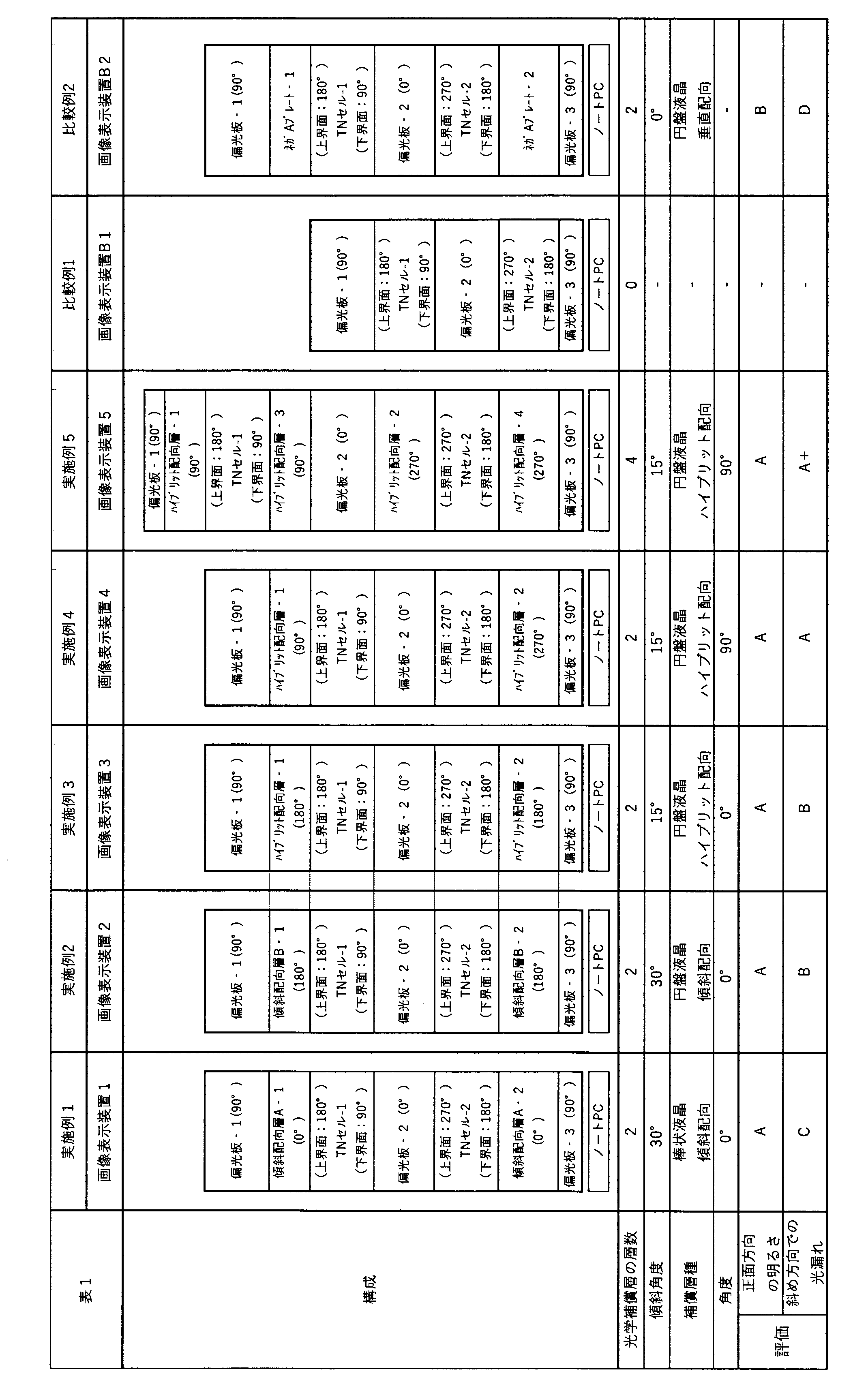
表1に示すように、本発明の視野角制御システムは、所望の効果を示すことが確認された。
実施例1と2との比較より、光学補償層の材料として円盤状液晶化合物を用いると、より効果が優れることが確認された。
実施例3と4との比較より、第1光学補償層において液晶化合物の光学軸を第1光学補償層の表面に投影してなる投影軸と、第1液晶セル中の液晶層の第1光学補償層側の表面における面内遅相軸とのなす角度が、45~135°であり、第2光学補償層において液晶化合物の光学軸を第2光学補償層の表面に投影してなる投影軸と、第2液晶セル中の液晶層の第2光学補償層側の表面における面内遅相軸とのなす角度が、45~135°である場合に、より効果が優れることが確認された。
実施例5と他の実施例との比較より、第3光学補償層および第4光学補償層を用いた場合、より効果が優れることが確認された。
As shown in Table 1, it was confirmed that the viewing angle control system of the present invention exhibited the desired effects.
From a comparison between Examples 1 and 2, it was confirmed that the use of a discotic liquid crystal compound as the material for the optical compensation layer provided a more excellent effect.
A comparison between Examples 3 and 4 confirmed that the effect was superior when the angle between the projection axis formed by projecting the optical axis of the liquid crystal compound onto the surface of the first optical compensation layer in the first optical compensation layer and the in-plane slow axis on the surface of the liquid crystal layer on the first optical compensation layer side in the first liquid crystal cell was 45 to 135°, and when the angle between the projection axis formed by projecting the optical axis of the liquid crystal compound onto the surface of the second optical compensation layer in the second optical compensation layer and the in-plane slow axis on the surface of the liquid crystal layer on the second optical compensation layer side in the second liquid crystal cell was 45 to 135°.
From a comparison between Example 5 and the other Examples, it was confirmed that a more excellent effect was obtained when the third optical compensation layer and the fourth optical compensation layer were used.
10 第1偏光子
12 第1光学補償層
14 第1液晶セル
16 第2偏光子
18 第2液晶セル
20,20A 第2光学補償層
22 第3偏光子
24,30 液晶層
26,28,32,34 基板
40 第3光学補償層
42 第4光学補償層
REFERENCE SIGNS
Claims (6)
第1光学補償層と、
第1液晶セルと、
第2偏光子と、
第2液晶セルと、
第2光学補償層と、
第3偏光子と、をこの順に有し、
前記第1液晶セルおよび前記第2液晶セルが、TNモードの液晶セルであり、
前記第1光学補償層が、前記第1光学補償層の法線方向、および、前記第1光学補償層の法線方向から傾いた方向から位相差を測定した際に、前記第1光学補償層の法線方向から傾いた方向において最も位相差が小さくなる層であり、
前記第2光学補償層が、前記第2光学補償層の法線方向、および、前記2光学補償層の法線方向から傾いた方向から位相差を測定した際に、前記第2光学補償層の法線方向から傾いた方向において最も位相差が小さくなる層である、視野角制御システム。 A first polarizer; and
A first optical compensation layer;
A first liquid crystal cell;
A second polarizer; and
A second liquid crystal cell;
A second optical compensation layer;
a third polarizer,
the first liquid crystal cell and the second liquid crystal cell are TN mode liquid crystal cells,
the first optical compensation layer is a layer in which, when a retardation is measured in a normal direction of the first optical compensation layer and in a direction tilted from the normal direction of the first optical compensation layer, the retardation is smallest in a direction tilted from the normal direction of the first optical compensation layer,
a viewing angle control system, wherein the second optical compensation layer is a layer that has the smallest phase difference in a direction tilted from the normal direction of the second optical compensation layer when the phase difference is measured from a normal direction of the second optical compensation layer and a direction tilted from the normal direction of the second optical compensation layer.
前記第2光学補償層において前記液晶化合物の光学軸を前記第2光学補償層の表面に投影してなる投影軸と、前記第2液晶セル中の液晶層の前記第2光学補償層側の表面における面内遅相軸とのなす角度が、45~135°である、請求項2に記載の視野角制御システム。 an angle between a projection axis obtained by projecting an optical axis of the liquid crystal compound onto a surface of the first optical compensation layer and an in-plane slow axis of a surface of a liquid crystal layer in the first liquid crystal cell on the side of the first optical compensation layer is 45 to 135°;
3. The viewing angle control system according to claim 2, wherein an angle between a projection axis obtained by projecting an optical axis of the liquid crystal compound in the second optical compensation layer onto a surface of the second optical compensation layer and an in-plane slow axis of a surface of a liquid crystal layer in the second liquid crystal cell on the second optical compensation layer side is 45 to 135°.
前記第2偏光子と、前記第2液晶セルとの間に、さらに第4光学補償層を有し、
前記第3光学補償層が、前記第3光学補償層の法線方向、および、前記3光学補償層の法線方向から傾いた方向から位相差を測定した際に、前記3光学補償層の法線方向から傾いた方向において最も位相差が小さくなる層であり、
前記第4光学補償層が、前記第4光学補償層の法線方向、および、前記第4光学補償層の法線方向から傾いた方向から位相差を測定した際に、前記第4光学補償層の法線方向から傾いた方向において最も位相差が小さくなる層である、請求項1に記載の視野角制御システム。 a third optical compensation layer is further provided between the first liquid crystal cell and the second polarizer,
a fourth optical compensation layer is further provided between the second polarizer and the second liquid crystal cell,
the third optical compensation layer is a layer in which, when a retardation is measured from a normal direction of the third optical compensation layer and a direction tilted from the normal direction of the third optical compensation layer, a retardation is smallest in a direction tilted from the normal direction of the third optical compensation layer,
2. The viewing angle control system according to claim 1, wherein the fourth optical compensation layer is a layer that has the smallest phase difference in a direction tilted from the normal direction of the fourth optical compensation layer when the phase difference is measured from a normal direction of the fourth optical compensation layer and a direction tilted from the normal direction of the fourth optical compensation layer.
An image display device comprising an image display element and the viewing angle control system according to any one of claims 1 to 5.
Priority Applications (1)
| Application Number | Priority Date | Filing Date | Title |
|---|---|---|---|
| CN202480029979.7A CN121153005A (en) | 2023-05-23 | 2024-05-14 | Viewing angle control system and image display device |
Applications Claiming Priority (2)
| Application Number | Priority Date | Filing Date | Title |
|---|---|---|---|
| JP2023-084751 | 2023-05-23 | ||
| JP2023084751 | 2023-05-23 |
Related Child Applications (1)
| Application Number | Title | Priority Date | Filing Date |
|---|---|---|---|
| US19/357,127 Continuation US20260036838A1 (en) | 2023-05-23 | 2025-10-14 | Viewing angle control system and image display apparatus |
Publications (1)
| Publication Number | Publication Date |
|---|---|
| WO2024241966A1 true WO2024241966A1 (en) | 2024-11-28 |
Family
ID=93589259
Family Applications (1)
| Application Number | Title | Priority Date | Filing Date |
|---|---|---|---|
| PCT/JP2024/017802 Pending WO2024241966A1 (en) | 2023-05-23 | 2024-05-14 | Viewing angle control system and image display device |
Country Status (3)
| Country | Link |
|---|---|
| CN (1) | CN121153005A (en) |
| TW (1) | TW202514232A (en) |
| WO (1) | WO2024241966A1 (en) |
Citations (3)
| Publication number | Priority date | Publication date | Assignee | Title |
|---|---|---|---|---|
| US20210026194A1 (en) * | 2019-07-23 | 2021-01-28 | Innolux Corporation | Electronic device |
| JP2021156943A (en) * | 2020-03-25 | 2021-10-07 | 株式会社ジャパンディスプレイ | Display devices, vehicle display devices, and vehicles |
| JP2022160895A (en) * | 2021-04-07 | 2022-10-20 | 株式会社ジャパンディスプレイ | Display device |
-
2024
- 2024-05-14 WO PCT/JP2024/017802 patent/WO2024241966A1/en active Pending
- 2024-05-14 CN CN202480029979.7A patent/CN121153005A/en active Pending
- 2024-05-21 TW TW113118790A patent/TW202514232A/en unknown
Patent Citations (3)
| Publication number | Priority date | Publication date | Assignee | Title |
|---|---|---|---|---|
| US20210026194A1 (en) * | 2019-07-23 | 2021-01-28 | Innolux Corporation | Electronic device |
| JP2021156943A (en) * | 2020-03-25 | 2021-10-07 | 株式会社ジャパンディスプレイ | Display devices, vehicle display devices, and vehicles |
| JP2022160895A (en) * | 2021-04-07 | 2022-10-20 | 株式会社ジャパンディスプレイ | Display device |
Also Published As
| Publication number | Publication date |
|---|---|
| CN121153005A (en) | 2025-12-16 |
| TW202514232A (en) | 2025-04-01 |
Similar Documents
| Publication | Publication Date | Title |
|---|---|---|
| CN101542364B (en) | Liquid crystal display device, laminated polarizing plate, and polarized light source device | |
| JP6667983B2 (en) | Laminate and manufacturing method thereof, polarizing plate, liquid crystal display, organic EL display | |
| CN100510805C (en) | optical film and liquid crystal display device | |
| JP4902516B2 (en) | Viewing angle control system and image display device | |
| CN1316264C (en) | Optical films and display system | |
| CN100424565C (en) | Retardation film with vertically aligned liquid crystal film and preparation method thereof | |
| JP6952779B2 (en) | Liquid crystal display | |
| WO2021177308A1 (en) | Visual angle control system and image display device | |
| JP5292457B2 (en) | Viewing angle control system and image display device | |
| CN100392500C (en) | Liquid crystal display device | |
| WO2008059721A1 (en) | Elliptic polarizing plate and vertically aligned liquid crystal display using the same | |
| WO2009150779A1 (en) | Elliptical light polarizing plate and vertically oriented liquid crystal display device using the same | |
| JP2024022690A (en) | Optical laminates, image display devices and glass composites | |
| JP2008009403A (en) | Elliptical polarizing plate, manufacturing method of elliptical polarizing plate, and liquid crystal display device | |
| CN101772718A (en) | Elliptical polarizing plate, manufacturing method thereof, and liquid crystal display device using the same | |
| JPWO2018207797A1 (en) | Liquid crystal display | |
| JP2024149527A (en) | Optical films, circular polarizing plates, organic electroluminescence displays | |
| JP3408930B2 (en) | Wide viewing angle polarizer | |
| WO2014157182A1 (en) | Laminated polarizing plate and horizontal alignment liquid crystal display device | |
| JP2008129175A (en) | Elliptical polarizing plate and vertical alignment type liquid crystal display device using the same | |
| JP2020052411A (en) | Laminate and manufacturing method of the same, polarization plate, liquid crystal display device, and organic el display device | |
| WO2024241966A1 (en) | Viewing angle control system and image display device | |
| JP2007072213A (en) | Viewing angle compensation plate for vertical alignment type liquid crystal display device and vertical alignment type liquid crystal display device using the same | |
| US20260036838A1 (en) | Viewing angle control system and image display apparatus | |
| JP7420956B2 (en) | Optical films, circularly polarizing plates, organic electroluminescent display devices |
Legal Events
| Date | Code | Title | Description |
|---|---|---|---|
| 121 | Ep: the epo has been informed by wipo that ep was designated in this application |
Ref document number: 24810973 Country of ref document: EP Kind code of ref document: A1 |
|
| ENP | Entry into the national phase |
Ref document number: 2025522336 Country of ref document: JP Kind code of ref document: A |
|
| WWE | Wipo information: entry into national phase |
Ref document number: 2025522336 Country of ref document: JP |
|
| WWE | Wipo information: entry into national phase |
Ref document number: CN2024800299797 Country of ref document: CN |
|
| NENP | Non-entry into the national phase |
Ref country code: DE |