WO2024195629A1 - Thin-film transistor and electronic device - Google Patents
Thin-film transistor and electronic device Download PDFInfo
- Publication number
- WO2024195629A1 WO2024195629A1 PCT/JP2024/009575 JP2024009575W WO2024195629A1 WO 2024195629 A1 WO2024195629 A1 WO 2024195629A1 JP 2024009575 W JP2024009575 W JP 2024009575W WO 2024195629 A1 WO2024195629 A1 WO 2024195629A1
- Authority
- WO
- WIPO (PCT)
- Prior art keywords
- oxide semiconductor
- semiconductor layer
- film transistor
- film
- crystal
- Prior art date
- Legal status (The legal status is an assumption and is not a legal conclusion. Google has not performed a legal analysis and makes no representation as to the accuracy of the status listed.)
- Ceased
Links
Images


Classifications
-
- H—ELECTRICITY
- H10—SEMICONDUCTOR DEVICES; ELECTRIC SOLID-STATE DEVICES NOT OTHERWISE PROVIDED FOR
- H10D—INORGANIC ELECTRIC SEMICONDUCTOR DEVICES
- H10D30/00—Field-effect transistors [FET]
- H10D30/60—Insulated-gate field-effect transistors [IGFET]
- H10D30/67—Thin-film transistors [TFT]
- H10D30/674—Thin-film transistors [TFT] characterised by the active materials
- H10D30/6755—Oxide semiconductors, e.g. zinc oxide, copper aluminium oxide or cadmium stannate
-
- H—ELECTRICITY
- H10—SEMICONDUCTOR DEVICES; ELECTRIC SOLID-STATE DEVICES NOT OTHERWISE PROVIDED FOR
- H10D—INORGANIC ELECTRIC SEMICONDUCTOR DEVICES
- H10D30/00—Field-effect transistors [FET]
- H10D30/01—Manufacture or treatment
- H10D30/021—Manufacture or treatment of FETs having insulated gates [IGFET]
- H10D30/031—Manufacture or treatment of FETs having insulated gates [IGFET] of thin-film transistors [TFT]
-
- H—ELECTRICITY
- H10—SEMICONDUCTOR DEVICES; ELECTRIC SOLID-STATE DEVICES NOT OTHERWISE PROVIDED FOR
- H10D—INORGANIC ELECTRIC SEMICONDUCTOR DEVICES
- H10D30/00—Field-effect transistors [FET]
- H10D30/60—Insulated-gate field-effect transistors [IGFET]
- H10D30/67—Thin-film transistors [TFT]
-
- H—ELECTRICITY
- H10—SEMICONDUCTOR DEVICES; ELECTRIC SOLID-STATE DEVICES NOT OTHERWISE PROVIDED FOR
- H10D—INORGANIC ELECTRIC SEMICONDUCTOR DEVICES
- H10D30/00—Field-effect transistors [FET]
- H10D30/60—Insulated-gate field-effect transistors [IGFET]
- H10D30/67—Thin-film transistors [TFT]
- H10D30/6704—Thin-film transistors [TFT] having supplementary regions or layers in the thin films or in the insulated bulk substrates for controlling properties of the device
- H10D30/6723—Thin-film transistors [TFT] having supplementary regions or layers in the thin films or in the insulated bulk substrates for controlling properties of the device having light shields
-
- H—ELECTRICITY
- H10—SEMICONDUCTOR DEVICES; ELECTRIC SOLID-STATE DEVICES NOT OTHERWISE PROVIDED FOR
- H10D—INORGANIC ELECTRIC SEMICONDUCTOR DEVICES
- H10D30/00—Field-effect transistors [FET]
- H10D30/60—Insulated-gate field-effect transistors [IGFET]
- H10D30/67—Thin-film transistors [TFT]
- H10D30/6729—Thin-film transistors [TFT] characterised by the electrodes
- H10D30/673—Thin-film transistors [TFT] characterised by the electrodes characterised by the shapes, relative sizes or dispositions of the gate electrodes
- H10D30/6736—Thin-film transistors [TFT] characterised by the electrodes characterised by the shapes, relative sizes or dispositions of the gate electrodes characterised by the shape of gate insulators
-
- H—ELECTRICITY
- H10—SEMICONDUCTOR DEVICES; ELECTRIC SOLID-STATE DEVICES NOT OTHERWISE PROVIDED FOR
- H10D—INORGANIC ELECTRIC SEMICONDUCTOR DEVICES
- H10D30/00—Field-effect transistors [FET]
- H10D30/60—Insulated-gate field-effect transistors [IGFET]
- H10D30/67—Thin-film transistors [TFT]
- H10D30/6757—Thin-film transistors [TFT] characterised by the structure of the channel, e.g. transverse or longitudinal shape or doping profile
Definitions
- One embodiment of the present invention relates to a thin-film transistor including an oxide semiconductor (Poly-OS) film having a polycrystalline structure.
- Another embodiment of the present invention relates to an electronic device including a thin-film transistor.
- thin-film transistors that use oxide semiconductor films as channels instead of silicon semiconductor films made of amorphous silicon, low-temperature polysilicon, and single-crystal silicon have been developed (see, for example, Patent Documents 1 to 6).
- Thin-film transistors that include such oxide semiconductor films can be formed with a simple structure and low-temperature process, similar to thin-film transistors that include amorphous silicon films.
- Thin-film transistors that include oxide semiconductor films are also known to have higher field-effect mobility than thin-film transistors that include amorphous silicon films.
- a thin film transistor includes a substrate, a metal oxide layer provided on the substrate, an oxide semiconductor layer including a plurality of crystal grains provided in contact with the metal oxide layer, a gate electrode provided on the oxide semiconductor layer, and a gate insulating layer provided between the oxide semiconductor layer and the gate electrode, and when the crystal orientation at each of a plurality of measurement points of the oxide semiconductor layer is obtained based on an electron diffraction pattern obtained by transmitting an electron beam irradiated from a direction intersecting the film thickness direction of the oxide semiconductor layer through the oxide semiconductor layer, the average value of the KAM values calculated at the plurality of measurement points is 0.6° or more.
- An electronic device includes the above-described thin-film transistor.
- FIG. 1 is a schematic cross-sectional view showing a configuration of a thin film transistor according to one embodiment of the present invention.
- 1 is a schematic plan view illustrating a configuration of a thin film transistor according to an embodiment of the present invention.
- FIG. 1 is a schematic diagram illustrating a TEM-ED mapping method.
- 2 is a flowchart showing a method for manufacturing a thin film transistor according to an embodiment of the present invention.
- 1A to 1C are schematic cross-sectional views showing a method for manufacturing a thin film transistor according to an embodiment of the present invention.
- 1A to 1C are schematic cross-sectional views showing a method for manufacturing a thin film transistor according to an embodiment of the present invention.
- 1A to 1C are schematic cross-sectional views showing a method for manufacturing a thin film transistor according to an embodiment of the present invention.
- 1A to 1C are schematic cross-sectional views showing a method for manufacturing a thin film transistor according to an embodiment of the present invention.
- 1A to 1C are schematic cross-sectional views showing a method for manufacturing a thin film transistor according to an embodiment of the present invention.
- 1A to 1C are schematic cross-sectional views showing a method for manufacturing a thin film transistor according to an embodiment of the present invention.
- 1A to 1C are schematic cross-sectional views showing a method for manufacturing a thin film transistor according to an embodiment of the present invention.
- 1A to 1C are schematic cross-sectional views showing a method for manufacturing a thin film transistor according to an embodiment of the present invention.
- 1 is a schematic diagram illustrating an electronic device according to an embodiment of the present invention.
- 11 is an inverse pole figure of an oxide semiconductor layer (Poly-OS film) of a sample according to an embodiment of the present invention.
- 13 is an IPF map of an oxide semiconductor layer (Poly-OS film) of a sample according to an embodiment of the present invention. 1 shows a KAM map of an oxide semiconductor layer (Poly-OS film) of an example sample. 13 is a graph showing the distribution of KAM values of oxide semiconductor layers (Poly-OS films) of example samples. 13 is a graph showing the depth-average KAM value in oxide semiconductor layers (Poly-OS films) of example samples.
- the direction from the substrate toward the oxide semiconductor layer is referred to as “up” or “upper”. Conversely, the direction from the oxide semiconductor layer toward the substrate is referred to as “down” or “lower”.
- the terms “up” or “lower” are used in the explanation, but for example, the vertical relationship between the substrate and the oxide semiconductor layer may be arranged in a direction different from that shown in the figure.
- the expression “oxide semiconductor layer on a substrate” merely describes the vertical relationship between the substrate and the oxide semiconductor layer as described above, and other members may be arranged between the substrate and the oxide semiconductor layer.
- Up or “lower” refers to the order of stacking in a structure in which multiple layers are stacked, and when a pixel electrode is expressed above a thin film transistor, the thin film transistor and the pixel electrode may not overlap in a planar view. On the other hand, when a pixel electrode is expressed vertically above a thin film transistor, the thin film transistor and the pixel electrode overlap in a planar view.
- film and “layer” may be used interchangeably in some cases.
- the term “display device” refers to a structure that displays an image using an electro-optical layer.
- the term display device may refer to a display panel that includes an electro-optical layer, or a structure in which other optical components (e.g., polarizing components, backlights, touch panels, etc.) are attached to a display cell.
- the "electro-optical layer” may include a liquid crystal layer, an electroluminescent (EL) layer, an electrochromic (EC) layer, and an electrophoretic layer, unless a technical contradiction occurs.
- the thin film transistor 10 can be used in, for example, a display device, an integrated circuit (IC) such as a microprocessor (Micro-Processing Unit: MPU), or a memory circuit.
- IC integrated circuit
- MPU Micro-Processing Unit
- FIG. 1 is a schematic cross-sectional view showing the configuration of the thin film transistor 10 according to one embodiment of the present invention.
- Figure 2 is a schematic plan view showing the configuration of the thin film transistor according to one embodiment of the present invention.
- Figure 1 is a cross-sectional view taken along line AA' in Figure 2.
- the thin film transistor 10 includes a substrate 100, a light-shielding layer 105, a first insulating layer 110, a second insulating layer 120, a metal oxide layer 130, an oxide semiconductor layer 140, a gate insulating layer 150, a gate electrode 160, a third insulating layer 170, a fourth insulating layer 180, a source electrode 201, and a drain electrode 203.
- the light-shielding layer 105 is provided on the substrate 100.
- the first insulating layer 110 covers the upper surface and end surfaces of the light-shielding layer 105 and is provided on the substrate 100.
- the second insulating layer 120 is provided on the first insulating layer 110.
- the metal oxide layer 130 is provided on the second insulating layer 120.
- the oxide semiconductor layer 140 is provided on the metal oxide layer 130.
- the oxide semiconductor layer 140 is in contact with the metal oxide layer 130.
- the gate insulating layer 150 covers the upper surface and end surfaces of the oxide semiconductor layer 140 and the end surfaces of the metal oxide layer 130, and is provided on the second insulating layer 120.
- the gate electrode 160 overlaps the oxide semiconductor layer 140 and is provided on the gate insulating layer 150.
- the third insulating layer 170 covers the upper surface and end surfaces of the gate electrode 160 and is provided on the gate insulating layer 150.
- the fourth insulating layer 180 is provided on the third insulating layer 170.
- the gate insulating layer 150, the third insulating layer 170, and the fourth insulating layer 180 are provided with openings 171 and 173 through which a part of the upper surface of the oxide semiconductor layer 140 is exposed.
- the source electrode 201 is provided on the fourth insulating layer 180 and inside the opening 171, and is in contact with the oxide semiconductor layer 140.
- the drain electrode 203 is provided on the fourth insulating layer 180 and inside the opening 173, and is in contact with the oxide semiconductor layer 140.
- the source-drain electrode 200 when there is no particular distinction between the source electrode 201 and the drain electrode 203, they may be collectively referred to as the source-drain electrode 200.
- the oxide semiconductor layer 140 is divided into a source region S, a drain region D, and a channel region CH with respect to the gate electrode 160. That is, the oxide semiconductor layer 140 includes the channel region CH overlapping with the gate electrode 160, and the source region S and the drain region D not overlapping with the gate electrode 160. In the film thickness direction of the oxide semiconductor layer 140, the end of the channel region CH coincides with the end of the gate electrode 160.
- the channel region CH has semiconductor properties.
- Each of the source region S and the drain region D has conductor properties. Therefore, the electrical conductivity of the source region S and the drain region D is greater than the electrical conductivity of the channel region CH.
- the source electrode 201 and the drain electrode 203 are in contact with the source region S and the drain region D, respectively, and are electrically connected to the oxide semiconductor layer 140.
- the oxide semiconductor layer 140 may have a single-layer structure or a multilayer structure.
- each of the light-shielding layer 105 and the gate electrode 160 has a constant width in the D1 direction and extends in the D2 direction perpendicular to the D1 direction.
- the width of the light-shielding layer 105 is greater than the width of the gate electrode 160.
- the channel region CH completely overlaps with the light-shielding layer 105.
- the D1 direction corresponds to the direction in which a current flows from the source electrode 201 to the drain electrode 203 through the oxide semiconductor layer 140. Therefore, the length of the channel region CH in the D1 direction is the channel length L, and the width of the channel region CH in the D2 direction is the channel width W.
- the substrate 100 can support each layer constituting the thin film transistor 10.
- a rigid substrate having light transmission properties such as a glass substrate, a quartz substrate, or a sapphire substrate
- a rigid substrate having no light transmission properties such as a silicon substrate
- a flexible substrate having light transmission properties such as a polyimide resin substrate, an acrylic resin substrate, a siloxane resin substrate, or a fluororesin substrate, can also be used as the substrate.
- impurities may be introduced into the above-mentioned resin substrate.
- a substrate in which a silicon oxide film or a silicon nitride film is formed on the above-mentioned rigid substrate or flexible substrate can also be used as the substrate 100.
- the light-shielding layer 105 can reflect or absorb external light. As described above, the light-shielding layer 105 is provided with an area larger than the channel region CH of the oxide semiconductor layer 140, and therefore can block external light incident on the channel region CH. For example, aluminum (Al), copper (Cu), titanium (Ti), molybdenum (Mo), or tungsten (W), or an alloy or compound thereof, can be used as the light-shielding layer 105. In addition, if electrical conductivity is not required, the light-shielding layer 105 does not necessarily need to contain a metal. For example, a black matrix made of a black resin can be used as the light-shielding layer 105.
- the light-shielding layer 105 may have a single-layer structure or a laminated structure.
- the light-shielding layer 105 may have a laminated structure of a red color filter, a green color filter, and a blue color filter.
- the first insulating layer 110, the second insulating layer 120, the third insulating layer 170, and the fourth insulating layer 180 can prevent impurities from diffusing into the oxide semiconductor layer 140.
- the first insulating layer 110 and the second insulating layer 120 can prevent the diffusion of impurities contained in the substrate 100
- the third insulating layer 170 and the fourth insulating layer 180 can prevent the diffusion of impurities (e.g., water) entering from the outside.
- silicon oxynitride (SiO x N y ) and aluminum oxynitride (AlO x N y ) are silicon compounds and aluminum compounds, respectively, containing nitrogen (N) at a ratio (x>y) smaller than that of oxygen (O).
- Silicon oxynitride ( SiNxOy ) and aluminum oxynitride ( AlNxOy ) are silicon compounds and aluminum compounds that contain a smaller ratio of oxygen than nitrogen (x> y ).
- Each of the first insulating layer 110, the second insulating layer 120, the third insulating layer 170, and the fourth insulating layer 180 may have a single-layer structure or a multilayer structure.
- each of the first insulating layer 110, the second insulating layer 120, the third insulating layer 170, and the fourth insulating layer 180 may have a planarizing function, or may have a function of releasing oxygen by heat treatment.
- the second insulating layer 120 has a function of releasing oxygen by heat treatment, oxygen is released from the second insulating layer 120 by the heat treatment performed in the manufacturing process of the thin film transistor 10, and the released oxygen can be supplied to the oxide semiconductor layer 140.
- the gate electrode 160, the source electrode 201, and the drain electrode 203 are conductive.
- copper (Cu), aluminum (Al), titanium (Ti), chromium (Cr), cobalt (Co), nickel (Ni), molybdenum (Mo), hafnium (Hf), tantalum (Ta), tungsten (W), or bismuth (Bi), or an alloy or compound thereof can be used for each of the gate electrode 160, the source electrode 201, and the drain electrode 203.
- Each of the gate electrode 160, the source electrode 201, and the drain electrode 203 may have a single-layer structure or a multilayer structure.
- the gate insulating layer 150 includes an oxide having insulating properties. Specifically, silicon oxide (SiO x ), silicon oxynitride (SiO x N y ), aluminum oxide (AlO x ), aluminum oxynitride (AlO x N y ), or the like is used as the gate insulating layer 150.
- the gate insulating layer 150 preferably has a composition close to a stoichiometric ratio.
- the gate insulating layer 150 preferably has few defects.
- the gate insulating layer 150 may be made of an oxide in which no defects are observed when evaluated by electron spin resonance (ESR).
- the metal oxide layer 130 includes a metal oxide having insulating properties. Specifically, a metal oxide having a band gap of 4 eV or more and 10.0 eV or less is used as the metal oxide layer 130.
- a metal oxide containing one or more metal elements selected from aluminum (Al), magnesium (Mg), calcium (Ca), scandium (Sc), gallium (Ga), germanium (Ge), strontium (Sr), nickel (Ni), tantalum (Ta), yttrium (Y), zirconium (Zr), barium (Ba), hafnium (Hf), cobalt (Co), and lanthanoid elements is used.
- a metal oxide containing aluminum e.g., aluminum oxide, etc.
- a metal oxide containing aluminum has high barrier properties against gases such as oxygen or hydrogen.
- the metal oxide layer 130 can also function as a buffer layer for the oxide semiconductor layer 140. For example, by subjecting the oxide semiconductor layer 140 in contact with the metal oxide layer 130 to a heat treatment, the crystallinity of the oxide semiconductor layer 140 can be improved.
- the oxide semiconductor film contains indium (In) and at least one or more metal elements (M) other than indium.
- the composition ratio of the oxide semiconductor film is preferably such that the atomic ratio of indium and at least one or more metal elements satisfies formula (1). In other words, the ratio of indium to all metal elements in the oxide semiconductor film is preferably 50% or more.
- the crystal structure of the oxide semiconductor film preferably has a bixbyite structure. By increasing the ratio of indium, an oxide semiconductor film having a bixbyite structure can be formed.
- the metal element other than indium is not limited to one type of metal element.
- the metal element other than indium may include multiple types of metal elements.
- the oxide semiconductor film can be formed by sputtering.
- the composition of the oxide semiconductor film formed by sputtering depends on the composition of the sputtering target. With a sputtering target having the above-mentioned composition, an oxide semiconductor film without compositional deviation of metal elements can be formed by sputtering. Therefore, the composition of the metal elements (indium and other metal elements) of the oxide semiconductor film may be the same as the composition of the metal elements of the sputtering target.
- the composition of the metal elements of the oxide semiconductor film can be specified based on the composition of the metal elements of the sputtering target. Note that this is not limited to the above because the oxygen contained in the oxide semiconductor film changes depending on the process conditions of the sputtering.
- the composition of the metal elements in the oxide semiconductor film can also be determined using X-ray fluorescence analysis or Electron Probe Micro Analyzer (EPMA) analysis. Furthermore, since the oxide semiconductor film has a polycrystalline structure, the composition of the oxide semiconductor film can be determined using X-ray diffraction (XRD) method. Specifically, the composition of the metal elements in the oxide semiconductor film can be determined based on the crystal structure and lattice constant of the oxide semiconductor film obtained by XRD method.
- XRD X-ray diffraction
- the oxide semiconductor film has a polycrystalline structure including a plurality of crystal grains. Although details will be described later, by using a polycrystalline oxide semiconductor (Poly-OS) technique, an oxide semiconductor film having a novel polycrystalline structure different from a conventional one can be formed. Therefore, hereinafter, the oxide semiconductor film having a polycrystalline structure according to this embodiment may be referred to as a Poly-OS film in order to distinguish it from a conventional oxide semiconductor film having a polycrystalline structure.
- Poly-OS polycrystalline oxide semiconductor
- the crystal grains contained in the Poly-OS film may be composed of multiple crystallites.
- the crystallite diameter is not particularly limited, but is preferably 1 nm or more, more preferably 10 nm or more, and even more preferably 15 nm or more.
- the crystallite diameter can be obtained using an electron beam diffraction method, an XRD method, or the like.
- the crystal structure of the Poly-OS film is not particularly limited, but is preferably a bixbyite structure.
- the crystal structure of the Poly-OS film can be identified using the XRD method or the electron beam diffraction method.
- the multiple crystal grains may have one type of crystal structure, or may have multiple types of crystal structures.
- the Poly-OS film has multiple types of crystal structures, it is preferable that one of the multiple types of crystal structures is a bixbyite structure.
- the crystal structure of the Poly-OS film is different from that of a conventional oxide semiconductor film having a polycrystalline structure.
- the inventors have found that the crystal grains contained in the Poly-OS film have characteristics different from those of the crystal grains contained in a conventional oxide semiconductor film.
- Such characteristics of the Poly-OS film can be obtained by measuring the crystal orientation (perpendicular to the crystal plane) using an electron diffraction pattern.
- the characteristics of the Poly-OS film can be measured using a TEM-ED mapping (Transmission Electron Microscopy Electron Diffraction Mapping) method.
- the TEM-ED mapping method is sometimes called the ACOM-TEM (Automated Crystal Orientation Mapping Transmission Electron Microscopy) method. The following describes the measurement of an oxide semiconductor film using the TEM-ED mapping method.
- FIG. 3 is a schematic diagram for explaining the TEM-ED mapping method.
- the TEM-ED mapping method is an analysis method in which an electron beam is irradiated onto a measurement region of an object to be measured, an electron diffraction pattern observed after passing through the object to be measured is analyzed, and the crystal orientation in the measurement region of the object to be measured is measured. By continuously analyzing the electron diffraction pattern at a plurality of measurement points in the measurement region, information on the crystal orientation within or between crystal grains can be obtained.
- a TEM sample 500 is used as the object to be measured. Therefore, the TEM-ED mapping method can obtain information on the crystal orientation in a smaller measurement region than the EBSD (Electron Back Scattered Diffraction) method using a SEM sample.
- EBSD Electro Back Scattered Diffraction
- the TEM-ED mapping method is applied to the oxide semiconductor layer 140 of the thin-film transistor 10
- a thin-film sample including a cross section of the oxide semiconductor layer 140 of the thin-film transistor 10 is used as the TEM sample 500.
- the TEM-ED mapping method is a measurement of a microscopic region using a TEM sample, and the step interval of the measurement points at which the electron beam diffraction pattern is observed is, for example, 1 nm or more, but is not limited to this. However, in measuring the crystal orientation, it is preferable to have a large number of measurement points in the film thickness direction of the oxide semiconductor layer 140.
- the step interval is 1/5 or less of the film thickness of the oxide semiconductor layer, preferably 1/10 or less, and more preferably 1/30 or less.
- a coordinate system based on the TEM sample 500 (ND (Normal Direction), TD (Transverse Direction), and RD (Reference Direction)) is used.
- ND Normal Direction
- TD Transverse Direction
- RD Reference Direction
- the normal direction to the surface of the TEM sample 500 is ND.
- ND, TD, and RD are mutually orthogonal.
- the electron beam is irradiated from the ND to the TEM 500.
- a coordinate system (x-axis, y-axis, and z-axis) based on the thin-film transistor 10 (or the oxide semiconductor layer 140) is shown, along with a coordinate system based on the TEM sample 500.
- the film thickness direction of the oxide semiconductor layer 140 is the z-axis.
- the x-axis, y-axis, and z-axis are mutually orthogonal. Therefore, the x-axis and y-axis are in-plane directions of the oxide semiconductor layer 140.
- ND, TD, and RD in the TEM-ED mapping method correspond to the y-axis, x-axis, and z-axis of the thin-film transistor 10, respectively.
- An inverse pole figure is an image illustrating crystal orientations in a specific direction of a coordinate system based on the TEM sample 500.
- the proportion of crystal orientations in each direction of the coordinate system of the TEM sample 500 is shown according to a predetermined index.
- the proportion of crystal orientations in a specific direction is color-coded according to a color key.
- IPF Map An IPF map is an image in which crystal orientations in a specific direction of a coordinate system based on the TEM sample 500 are illustrated as a distribution of crystal orientations on the surface of the TEM sample 500.
- crystal orientations at multiple measurement points are classified according to a predetermined index indicating the crystal orientation in each direction of the coordinate system of the TEM sample 500.
- the crystal orientations are color-coded according to a color key.
- a crystal grain is a crystalline region surrounded by a crystal grain boundary. Since the TEM-ED mapping method can obtain information about the crystal orientation, the crystal grain boundary can be defined based on the crystal orientation. In general, when the difference in crystal orientation between two adjacent measurement points exceeds 5°, it is defined that a crystal grain boundary exists between the two measurement points. Therefore, the above definition is also applied to the Poly-OS film.
- the TEM-ED mapping method is a measurement in a minute measurement region.
- a thin film sample having a surface along a cross section in the film thickness direction is used as the TEM sample 500, it is difficult to define the grain size of the crystal grains spreading in the plane of the oxide semiconductor layer 140. Therefore, in this embodiment, instead of the grain size, the length of the crystal grain obtained based on the cross section of the oxide semiconductor layer 140 in the measurement region is defined as the grain length. Specifically, the distance between two grain boundaries obtained in the cross section of the oxide semiconductor layer 140 is defined as the grain length. The grain length defined in this way may be calculated to be smaller than the grain size.
- the grain size of the crystal grains contained in the Poly-OS film is significantly larger than the grain size of the crystal grains contained in a conventional oxide semiconductor film. That is, the grain length defined as above in the Poly-OS film can be obtained as a value larger than the grain size of the crystal grains contained in a conventional oxide semiconductor film. Therefore, it is possible to compare the Poly-OS film with the conventional oxide semiconductor film by using the grain length defined as above.
- the crystal grain length is 100 nm or more, preferably 300 nm or more, and more preferably 500 nm or more.
- the upper limit of the crystal grain length is not particularly limited, but is 50 ⁇ m or less.
- the crystal grain length is preferably measured at the center of the film thickness.
- the crystal grains contained in the Poly-OS film have a large crystal grain length, and one crystal grain may form part of the upper surface and part of the lower surface of the Poly-OS film.
- the crystal grain boundary between two adjacent crystal grains is formed from the upper surface to the lower surface (or from the lower surface to the upper surface), but is not formed along the film thickness direction, and the position of the upper surface and the position of the lower surface of the crystal grain boundary may be misaligned.
- two adjacent crystal grains sandwiching a crystal grain boundary overlap each other in the film thickness direction of the Poly-OS film.
- the distance between the position of the upper surface and the position of the lower surface of the crystal grain boundary in the direction perpendicular to the film thickness direction of the Poly-OS film is, for example, 10 nm or more, preferably 20 nm or more, and more preferably 30 nm or more.
- KAM Kernel Average Misorientation
- the KAM (Kernel Average Misorientation) value is the average value of the crystal orientation misorientation between one measurement point in a crystal grain and all measurement points adjacent to that measurement point. The crystal orientation misorientation between two adjacent measurement points across a grain boundary is excluded from the calculation of the KAM value.
- the KAM value is a value that represents the change in crystal orientation within a crystal grain. As mentioned above, if the difference in crystal orientation between one measurement point and another measurement point adjacent to that measurement point exceeds 5°, it is considered to be a grain boundary. Therefore, the range of KAM values calculated based on adjacent measurement points within a crystal grain is 0° or more and 5° or less. A large KAM value means that there is a large change in local crystal orientation within the crystal grain, and that the crystal grain is highly distorted.
- the KAM value is calculated at each of the multiple measurement points. Therefore, a distribution diagram of the KAM value within the crystal grain can be created. In addition, the average value and standard deviation of the KAM value can be calculated.
- the average value of the KAM value is a value that represents one of the properties of the crystal grains contained in the Poly-OS film. Since the Poly-OS film has a large change in crystal orientation and contains many crystals with large distortion, the average value of the KAM value is larger than that of a conventional oxide semiconductor film having a polycrystalline structure.
- the average value of the KAM value in the Poly-OS film is 0.6° or more, preferably 0.7° or more, and more preferably 0.8° or more.
- the standard deviation of the KAM value is also a value that represents one of the properties of the crystal grains contained in the Poly-OS film.
- the standard deviation of the KAM value is 0.3° or more, preferably 0.35° or more, and more preferably 0.4° or more.
- the average KAM value increases as the step spacing between the measurement points increases. This is due to the large change in crystal orientation within the crystal grains contained in the Poly-OS film, and the tendency for the average KAM value to increase as the step spacing increases is also one of the characteristics of the Poly-OS film.
- the average value of the KAM values described above is the total average value of the KAM values (KAM AVE(total)) calculated using the KAM values of all the measurement points in the measurement region. Unless otherwise specified in this specification, the average value of the KAM values refers to the total average value of the KAM values (KAM AVE(total) ) . On the other hand, it is also possible to calculate the average value of the KAM values using some of the measurement points in the measurement region. For example, the film thickness of the Poly-OS film can be divided, and the average value of the KAM values of the measurement points included in the divided regions can be calculated.
- the average value of the KAM values calculated using some of the measurement points is different from the total average value of the KAM values (KAM AVE(total) ).
- the average value of the KAM value calculated by dividing the thickness of the Poly-OS film depends on the distance (depth) of the thickness of the Poly-OS film. Therefore, in this specification, the average value is sometimes referred to as the depth average value of the KAM value (KAM AVE(depth) ) to be distinguished from the total average value of the KAM values (KAM AVE(total) ).
- the Poly-OS film may be formed of one crystal grain from the top surface to the bottom surface.
- the crystal orientation also changes significantly in the thickness direction of the Poly-OS film.
- the depth average value (KAM AVE(depth) ) of the KAM value is different between the top end and bottom end (near the interface, for example, within 3 nm from the interface) and the center (near the center, for example, within 5 nm equidistant from the top end and bottom end) of the Poly-OS film.
- the depth average value (KAM AVE(depth) ) of the KAM value at each of the top end and bottom end of the Poly-OS film is 0.6° or more and less than 5.0°, and preferably 0.7° or more and less than 5.0°.
- the depth average value of the KAM value (KAM AVE(depth) ) at the center of the Poly-OS film is less than 0.6°.
- the difference in the depth average value of the KAM value (KAM AVE(depth) ) between the upper or lower end and the center of the Poly-OS film is 0.1° or more, preferably 0.15° or more, and further preferably 0.2° or more.
- the upper and lower surfaces of the Poly-OS film may have unevenness.
- the number of measurement points at the upper and lower ends is reduced, and the error in the depth average value of the KAM values (KAM AVE(depth)) at the upper and lower ends is likely to be large. Therefore, the depth average value of the KAM values (KAM AVE(depth) ) at the upper and lower ends may be calculated by considering a region in which the number of measurement points included in the divided region is 90% or more of the number of measurement points in the center (or a region in which the number of measurement points is 90% or more of the maximum number of measurement points ) as a valid region.
- the depth average value of the KAM values (KAM AVE(depth) ) at the upper and lower ends can be calculated without being affected by the unevenness formed on the upper and lower surfaces.
- the TEM-ED mapping method can obtain information about the crystal orientation within the crystal grains contained in the Poly-OS film. For example, when the Poly-OS film has a bixbyite structure, the TEM-ED mapping method can be observed to show that the Poly-OS film contains crystal grains with a crystal orientation of ⁇ 001>, ⁇ 101>, or ⁇ 111>.
- the crystal orientation ⁇ 001> represents [001] and its equivalents [100] and [010].
- the crystal orientation ⁇ 101> represents [101] and its equivalents [110] and [011].
- the crystal orientation ⁇ 111> represents [111].
- "1" may be "-1", and is considered to be an axis equivalent to each orientation.
- crystal orientations such as ⁇ hk0> (h ⁇ k, h and k are natural numbers), ⁇ hhl> (h ⁇ l, h and l are natural numbers), and ⁇ hkl> (h ⁇ k ⁇ l, h, k, and l are natural numbers).
- the crystal grains contained in the Poly-OS film have a characteristic that the crystal orientation changes greatly within the crystal grain.
- the average KAM value of the Poly-OS film is 0.6° or more.
- the crystal grain size of the crystal grain becomes small.
- the crystal grain length (or crystal grain size) of the crystal grain is large.
- the Poly-OS film is less susceptible to the influence of crystal grain boundaries because it contains crystal grains with a large crystal grain length (or crystal grain size). Therefore, in the thin-film transistor 10 that includes a Poly-OS film as the channel, the channel is less susceptible to the influence of crystal grain boundaries, grain boundary scattering is suppressed, and the field-effect mobility is improved.
- the configuration of the thin film transistor 10 has been described above, but the above-mentioned thin film transistor 10 is a so-called top-gate type transistor.
- the thin film transistor 10 can be modified in various ways.
- the thin film transistor 10 may be configured such that the light-shielding layer 105 functions as a gate electrode, and the first insulating layer 110 and the second insulating layer 120 function as gate insulating layers.
- the thin film transistor 10 is a so-called dual-gate type transistor.
- the light-shielding layer 105 when the light-shielding layer 105 is conductive, the light-shielding layer 105 may be a floating electrode or may be connected to the source electrode 201.
- the thin film transistor 10 may be a so-called bottom-gate type transistor in which the light-shielding layer 105 functions as a main gate electrode.
- FIG. 4 is a flowchart showing a method for manufacturing the thin film transistor 10 according to one embodiment of the present invention.
- Fig. 5 to Fig. 12 are schematic cross-sectional views showing a method for manufacturing the thin film transistor 10 according to one embodiment of the present invention.
- the method for manufacturing the thin-film transistor 10 includes steps S1010 to S1110. Below, steps S1010 to S1110 will be described in order, but the order of the steps may be reversed in the method for manufacturing the thin-film transistor 10. In addition, the method for manufacturing the thin-film transistor 10 may include additional steps.
- a light-shielding layer 105 having a predetermined pattern is formed on the substrate 100.
- the light-shielding layer 105 is patterned using a photolithography method.
- a first insulating layer 110 and a second insulating layer 120 are formed on the light-shielding layer 105 (see FIG. 5).
- the first insulating layer 110 and the second insulating layer 120 are formed using a CVD method.
- silicon nitride and silicon oxide are formed as the first insulating layer 110 and the second insulating layer 120, respectively.
- silicon nitride is used as the first insulating layer 110
- the first insulating layer 110 can block impurities that are diffused from the substrate 100 side to the oxide semiconductor layer 140.
- silicon oxide is used as the second insulating layer 120, the second insulating layer 120 can release oxygen by heat treatment.
- a metal oxide film 135 is formed on the second insulating layer 120 (see FIG. 6).
- the metal oxide film 135 is formed by a sputtering method.
- the thickness of the metal oxide film 135 is, for example, 2 nm to 51 nm, preferably 2 nm to 31 nm, more preferably 2 nm to 21 nm, and particularly preferably 2 nm to 11 nm.
- an oxide semiconductor film 145 is formed on the metal oxide film 135 (see FIG. 6).
- the oxide semiconductor film 145 is formed by a sputtering method.
- the thickness of the oxide semiconductor film 145 is, for example, 10 nm or more and 100 nm or less, preferably 15 nm or more and 70 nm or less, and more preferably 15 nm or more and 40 nm or less.
- the oxide semiconductor film 145 in step S1020 is amorphous.
- the oxide semiconductor film 145 after film formation and before heat treatment is amorphous. Therefore, it is preferable that the film formation conditions of the oxide semiconductor film 145 are such that the oxide semiconductor film 145 immediately after film formation is not crystallized as much as possible.
- the oxide semiconductor film 145 is formed by a sputtering method, the oxide semiconductor film 145 is formed while controlling the temperature of the film formation target (the substrate 100 and the layer formed on the substrate 100) to 100° C. or less, preferably 80° C. or less, and more preferably 50° C. or less.
- the oxide semiconductor film 145 is formed under a condition of low oxygen partial pressure.
- the oxygen partial pressure is 2% or more and 20% or less, preferably 3% or more and 15% or less, and more preferably 3% or more and less than 10%.
- the oxide semiconductor film 145 is patterned (see FIG. 7).
- the oxide semiconductor film 145 is patterned using a photolithography method.
- the oxide semiconductor film 145 may be etched by wet etching or dry etching.
- an acidic etchant may be used.
- oxalic acid, PAN, sulfuric acid, hydrogen peroxide, or hydrofluoric acid may be used as the etchant.
- step S1040 a heat treatment is performed on the oxide semiconductor film 145.
- the heat treatment performed in step S1040 is referred to as "OS annealing".
- OS annealing the oxide semiconductor film 145 is held at a predetermined temperature for a predetermined time.
- the predetermined temperature is 300° C. or higher and 500° C. or lower, and preferably 350° C. or higher and 450° C. or lower.
- the predetermined time (holding time) at the temperature is 15 minutes or higher and 120 minutes or lower, and preferably 30 minutes or higher and 60 minutes or lower.
- the OS annealing crystallizes the oxide semiconductor film 145, and an oxide semiconductor layer 140 having a polycrystalline structure (i.e., an oxide semiconductor layer 140 including a Poly-OS film) is formed.
- the metal oxide film 135 is patterned to form the metal oxide layer 130 (FIG. 8).
- the metal oxide film 135 is etched using the oxide semiconductor layer 140 as a mask.
- the photolithography process can be omitted.
- the metal oxide film 135 may be etched by wet etching or dry etching. For example, diluted hydrofluoric acid (DHF) is used in wet etching.
- DHF diluted hydrofluoric acid
- the gate insulating layer 150 is formed on the oxide semiconductor layer 140 (see FIG. 9).
- the gate insulating layer 150 is formed using a CVD method.
- silicon oxide is formed as the gate insulating layer 150.
- the gate insulating layer 150 may be formed at a film formation temperature of 350° C. or higher.
- the thickness of the gate insulating layer 150 is 50 nm or more and 300 nm or less, preferably 60 nm or more and 200 nm or less, and more preferably 70 nm or more and 150 nm or less.
- step S1060 a heat treatment is performed on the oxide semiconductor layer 140.
- the heat treatment performed in step S1060 is referred to as "oxidation annealing.”
- oxidation annealing When the gate insulating layer 150 is formed on the oxide semiconductor layer 140, many oxygen defects are generated on the upper and side surfaces of the oxide semiconductor layer 140.
- oxygen is supplied from the second insulating layer 120 and the gate insulating layer 150 to the oxide semiconductor layer 140, and the oxygen defects are repaired.
- a gate electrode 160 having a predetermined pattern is formed on the gate insulating layer 150 (see FIG. 10).
- the gate electrode 160 is formed by sputtering or atomic layer deposition, and the gate electrode 160 is patterned using photolithography.
- a source region S and a drain region D are formed in the oxide semiconductor layer 140 (see FIG. 10).
- the source region S and the drain region D are formed by ion implantation.
- impurities are implanted into the oxide semiconductor layer 140 through the gate insulating layer 150 using the gate electrode 160 as a mask.
- argon (Ar), phosphorus (P), or boron (B) is used as the implanted impurity.
- oxygen vacancies are generated by the ion implantation, and hydrogen is trapped in the generated oxygen vacancies. This reduces the resistance of the source region S and the drain region D.
- impurities are not implanted, so no oxygen vacancies are generated and the resistance of the channel region CH does not decrease.
- the gate insulating layer 150 may also contain impurities such as argon (Ar), phosphorus (P), or boron (B).
- a third insulating layer 170 and a fourth insulating layer 180 are formed on the gate insulating layer 150 and the gate electrode 160 (see FIG. 11).
- the third insulating layer 170 and the fourth insulating layer 180 are formed using a CVD method.
- silicon oxide and silicon nitride are formed as the third insulating layer 170 and the fourth insulating layer 180, respectively.
- the thickness of the third insulating layer 170 is 50 nm or more and 500 nm or less.
- the thickness of the fourth insulating layer 180 is also 50 nm or more and 500 nm or less.
- openings 171 and 173 are formed in the gate insulating layer 150, the third insulating layer 170, and the fourth insulating layer 180 (see FIG. 12). By forming the openings 171 and 173, the source region S and the drain region D of the oxide semiconductor layer 140 are exposed.
- a source electrode 201 is formed on the fourth insulating layer 180 and inside the opening 171
- a drain electrode 203 is formed on the fourth insulating layer 180 and inside the opening 173.
- the source electrode 201 and the drain electrode 203 are formed as the same layer. Specifically, the source electrode 201 and the drain electrode 203 are formed by patterning a single conductive film that has been deposited. Through these steps, the thin-film transistor 10 shown in FIG. 1 is manufactured.
- the oxide semiconductor layer 140 includes a Poly-OS film having a novel crystal structure.
- the Poly-OS film has a large change in crystal orientation and includes crystal grains with a large crystal grain length (or crystal grain size). Therefore, in the thin film transistor 10 including the Poly-OS film as the channel, the channel as a whole is less susceptible to the influence of the crystal grain boundaries. It is also considered that the crystal orientation within the crystal grains changes so as to improve the lattice matching at the crystal grain boundaries, and as a result, crystal grain boundaries with fewer defects are generated. For these reasons, in the thin film transistor 10 including the Poly-OS film as the channel, grain boundary scattering is suppressed and the field effect mobility is improved.
- FIG. 13 is a schematic diagram showing an electronic device 1000 according to one embodiment of the present invention.
- FIG. 13 shows a smartphone, which is an example of the electronic device 1000.
- the electronic device 1000 includes a display device 1100 with curved sides.
- the display device 1100 includes a plurality of pixels for displaying an image, and the plurality of pixels are controlled by a pixel circuit, a drive circuit, and the like.
- the pixel circuit and drive circuit include the thin-film transistor 10 described in the first embodiment.
- the thin-film transistor 10 has high field-effect mobility, and therefore improves the responsiveness of the pixel circuit and the drive circuit, and as a result, the performance of the electronic device 1000 can be improved.
- the electronic device 1000 is not limited to a smartphone.
- the electronic device 1000 also includes electronic devices having a display device, such as a watch, a tablet, a notebook computer, a car navigation system, or a television.
- the thin-film transistor 10 described in the first embodiment can be applied to any electronic device, regardless of whether or not it has a display device.
- oxide semiconductor layer specifically, the Poly-OS film
- a thin film transistor was fabricated using the manufacturing method described in the first embodiment.
- a sputtering target in which indium is 70% in atomic ratio to all metal elements contained in the sintered body was used to form an oxide semiconductor layer with a thickness of 30 nm.
- the oxygen partial pressure during film formation was 5%, and the substrate temperature was controlled to be 100° C. or less.
- the OS annealing process the ultimate temperature was controlled between 350° C. and 450° C. in an air atmosphere, and the ultimate temperature was held for 60 minutes.
- the chemical composition of the oxide semiconductor layer after the OS annealing process was the same as that of the sputtering target.
- Example sample A TEM sample (hereinafter referred to as an "example sample”) was prepared by sampling a cross section of a region including an oxide semiconductor layer of a thin film transistor by FIB processing, and a crystal orientation analysis of a Poly-OS film included in the oxide semiconductor layer was performed by TEM-ED mapping.
- the measurement conditions for the TEM-ED mapping are shown in Table 1.
- An ASTAR manufactured by NanoMegas Corp. was used for the analysis of the crystal orientation.
- PDF powder diffraction file
- FIG. 14 is an inverse pole figure of the oxide semiconductor layer (Poly-OS film) of the example sample.
- FIG. 14 shows inverse pole figures for ND, TD, and RD.
- the proportion of the crystal orientation increases according to the value of the index shown in FIG. 14 (for example, the index may be a color key, and the proportion of the crystal orientation increases as the color changes from blue to red (the wavelength of visible light increases)).
- the index may be a color key
- the proportion of the crystal orientation increases as the color changes from blue to red (the wavelength of visible light increases)
- regions A1, A2, and A3 there are regions having large values, and it was found that there are specific crystal orientations with a large proportion.
- the proportion of the crystal orientation ⁇ 111> is larger than that of the crystal orientation ⁇ 001> and the crystal orientation ⁇ 101>.
- IPF map 15 is an IPF map of an oxide semiconductor layer (Poly-OS film) of an example sample. IPF maps for ND, TD, and RD are shown in Fig. 15. In Fig. 15, the crystal orientation ⁇ 001>, the crystal orientation ⁇ 101>, the crystal orientation ⁇ 111>, and the crystal orientation ⁇ 011> are classified according to the indexes in the figure.
- the crystal orientation changed significantly and discontinuously.
- the discontinuous change in crystal orientation corresponds to a grain boundary, and in regions B1 and B2, a grain boundary was confirmed to have formed from the top surface to the bottom surface (or from the bottom surface to the top surface) of the oxide semiconductor layer.
- the grain length of one crystal grain between the grain boundary in region B1 and the grain boundary in region B2 was 1080 nm.
- one crystal grain formed part of the top surface and part of the bottom surface of the oxide semiconductor layer. In other words, the grain length was 10 times or more the thickness of the oxide semiconductor layer.
- the crystal orientations within the grains in the IPF map corresponded to the proportion of crystal orientations in the inverse pole figures described above.
- the main crystal orientation of the grains in the RD is the crystal orientation ⁇ 111>.
- the grain boundary in region B2 was not formed along the film thickness direction of the oxide semiconductor layer, but was significantly shifted from the film thickness direction of the oxide semiconductor layer. In other words, two adjacent crystal grains sandwiching the grain boundary in region B2 overlapped each other in the film thickness direction of the oxide semiconductor layer. In the direction perpendicular to the film thickness direction of the oxide semiconductor layer, the overlap distance of two adjacent crystal grains was 34 nm.
- KAM value 16 is a KAM map of the oxide semiconductor layer (Poly-OS film) of the example sample. Specifically, in FIG. 16, the KAM values of the measurement points in the measurement region are classified according to the values of the indices shown in FIG. 16 (for example, the indices may be a color key, and the KAM value increases from 0° to 5° as the color changes from blue to red (the wavelength of visible light increases)). Note that when the crystal orientation difference between two adjacent measurement points exceeds 5°, it is regarded as a grain boundary, and therefore the upper limit of the KAM value is 5°.
- FIG. 17 is a graph showing the distribution of the KAM values of the oxide semiconductor layer (Poly-OS film) of the example sample.
- the oxide semiconductor layer has not only a region having a KAM value near 0° (corresponding to the region shown in blue in the color key, hereinafter, for convenience of explanation, it will be referred to as the "blue region"), but also a region having a KAM value other than near 0° (corresponding to the region shown in green in the color key, hereinafter, for convenience of explanation, it will be referred to as the "green region”).
- the blue region spread in the center of the oxide semiconductor layer, and the green region spread near the surface (near the upper end and the lower end) of the oxide semiconductor layer.
- the TEM-ED mapping method is a measurement in a microscopic area, but in the case of the Poly-OS film, the total average value and standard deviation of the KAM value are large even in such a microscopic area. This means that there is a large change in the crystal orientation within the crystal grains of the Poly-OS film. Although the crystal grains contained in the Poly-OS film have a large crystal grain length (or crystal grain size), there is a large change in the local crystal orientation. This is one of the characteristics of the Poly-OS film that is not seen in conventional oxide semiconductor films having a polycrystalline structure.
- FIG. 18 is a graph showing the depth average value of the KAM value in the oxide semiconductor layer (Poly-OS film) of the example sample.
- the KAM values of the measurement points were collected for each distance from the interface between the gate insulating layer and the oxide semiconductor layer (depth of the oxide semiconductor layer), and the depth average value of the KAM value (KAM AVE(depth) ) was calculated, which is the average value.
- the depth average value of the KAM value (KAM AVE(depth) ) is the average value of the KAM values of some measurement points divided according to the depth of the oxide semiconductor layer.
- a region in which the number of measurement points included in the divided region is 90% or more of the number of measurement points in the center part was set as a valid region, and the depth average value of the KAM value (KAM AVE(depth) ) of the oxide semiconductor layer was calculated.
- the depth average value of the KAM value (KAM AVE(depth) ) is plotted against the thickness direction of the oxide semiconductor layer.
- the average depth value of the KAM value (KAM AVE(depth)) was larger at the upper end portion near the interface between the oxide semiconductor layer and the gate insulating layer and at the lower end portion near the interface between the oxide semiconductor layer and the metal oxide layer than at the central portion of the oxide semiconductor layer.
- the average depth values of the KAM value (KAM AVE(depth) ) at the central portion (depth 15 nm), upper end portion (depth 0 nm), and lower end portion (depth 32 nm) were 0.554°, 0.828°, and 0.802°, respectively.
- the difference in the average depth value of the KAM value (KAM AVE(depth) ) between the upper end portion and the central portion, and the difference between the lower end portion and the central portion were 0.2° or more.
- the above results indicate that there is a large change in crystal orientation near the interface of the oxide semiconductor layer.
- the local change in crystal orientation is also large in the film thickness direction.
- the crystal grain length (or crystal grain size) is small so that the distortion in the crystal grains is relieved, and it is difficult to form the oxide semiconductor film from the top to the bottom with a single crystal grain.
- the Poly-OS film it is possible to form the oxide semiconductor film from the top to the bottom with a single crystal grain that has a large change in crystal orientation. This is one of the characteristics of the Poly-OS film that is not seen in a conventional oxide semiconductor film having a polycrystalline structure.
Landscapes
- Thin Film Transistor (AREA)
Abstract
Description
本発明の一実施形態は、多結晶構造を有する酸化物半導体(Poly-OS)膜を含む薄膜トランジスタに関する。また、本発明の一実施形態は、薄膜トランジスタを含む電子機器に関する。 One embodiment of the present invention relates to a thin-film transistor including an oxide semiconductor (Poly-OS) film having a polycrystalline structure. Another embodiment of the present invention relates to an electronic device including a thin-film transistor.
近年、アモルファスシリコン、低温ポリシリコン、および単結晶シリコンなどを用いたシリコン半導体膜に替わり、酸化物半導体膜をチャネルとして用いる薄膜トランジスタの開発が進められている(例えば、特許文献1~特許文献6参照)。このような酸化物半導体膜を含む薄膜トランジスタは、アモルファスシリコン膜を含む薄膜トランジスタと同様に、単純な構造かつ低温プロセスで形成することができる。また、酸化物半導体膜を含む薄膜トランジスタは、アモルファスシリコン膜を含む薄膜トランジスタよりも高い電界効果移動度を有することが知られている。 In recent years, thin-film transistors that use oxide semiconductor films as channels instead of silicon semiconductor films made of amorphous silicon, low-temperature polysilicon, and single-crystal silicon have been developed (see, for example, Patent Documents 1 to 6). Thin-film transistors that include such oxide semiconductor films can be formed with a simple structure and low-temperature process, similar to thin-film transistors that include amorphous silicon films. Thin-film transistors that include oxide semiconductor films are also known to have higher field-effect mobility than thin-film transistors that include amorphous silicon films.
しかしながら、従来の酸化物半導体膜を含む薄膜トランジスタの電界効果移動度は、結晶性を有する酸化物半導体膜を用いた場合であってもそれ程大きくはない。そのため、薄膜トランジスタに用いられる酸化物半導体膜の結晶構造を改良し、薄膜トランジスタの電界効果移動度の向上が望まれていた。 However, the field effect mobility of thin film transistors including conventional oxide semiconductor films is not very high, even when a crystalline oxide semiconductor film is used. Therefore, there has been a demand for improving the crystal structure of the oxide semiconductor film used in thin film transistors and increasing the field effect mobility of thin film transistors.
本発明の一実施形態は、上記問題に鑑み、新規結晶構造を有する酸化物半導体膜を含む薄膜トランジスタを提供することを目的の一つとする。また、本発明の一実施形態は、薄膜トランジスタを含む電子機器を提供することを目的の一つとする。 In view of the above problems, one embodiment of the present invention has an object to provide a thin-film transistor including an oxide semiconductor film having a new crystal structure. Another object of one embodiment of the present invention is to provide an electronic device including a thin-film transistor.
本発明の一実施形態に係る薄膜トランジスタは、基板と、基板の上に設けられた金属酸化物層と、金属酸化物層と接して設けられる、複数の結晶粒を含む酸化物半導体層と、酸化物半導体層の上に設けられたゲート電極と、酸化物半導体層とゲート電極との間に設けられたゲート絶縁層と、を含み、酸化物半導体層の膜厚方向と交差する方向から照射される電子線が酸化物半導体層を透過して得られる電子回折パターンに基づいて酸化物半導体層の複数の測定点の各々における結晶方位が取得されるとき、複数の測定点において算出されるKAM値の平均値が0.6°以上である。 A thin film transistor according to one embodiment of the present invention includes a substrate, a metal oxide layer provided on the substrate, an oxide semiconductor layer including a plurality of crystal grains provided in contact with the metal oxide layer, a gate electrode provided on the oxide semiconductor layer, and a gate insulating layer provided between the oxide semiconductor layer and the gate electrode, and when the crystal orientation at each of a plurality of measurement points of the oxide semiconductor layer is obtained based on an electron diffraction pattern obtained by transmitting an electron beam irradiated from a direction intersecting the film thickness direction of the oxide semiconductor layer through the oxide semiconductor layer, the average value of the KAM values calculated at the plurality of measurement points is 0.6° or more.
本発明の一実施形態に係る電子機器は、上記薄膜トランジスタを含む。 An electronic device according to one embodiment of the present invention includes the above-described thin-film transistor.
以下に、本発明の各実施形態について、図面を参照しつつ説明する。以下の開示はあくまで一例にすぎない。当業者が、発明の主旨を保ちつつ、実施形態の構成を適宜変更することによって容易に想到し得る構成は、当然に本発明の範囲に含有される。説明をより明確にするため、図面は実際の態様に比べ、各部の幅、厚さ、形状等について模式的に表される場合がある。しかし、図示された形状はあくまで一例であって、本発明の解釈を限定しない。本明細書および図面において、既出の図に関して前述した構成要素と同様の構成要素には、同一の符号を付して、詳細な説明を適宜省略することがある。 Below, each embodiment of the present invention will be described with reference to the drawings. The following disclosure is merely an example. Configurations that a person skilled in the art can easily come up with by appropriately modifying the configuration of the embodiment while maintaining the gist of the invention are naturally included within the scope of the present invention. To make the explanation clearer, the drawings may show the width, thickness, shape, etc. of each part in a schematic manner compared to the actual form. However, the shapes shown are merely examples and do not limit the interpretation of the present invention. In this specification and drawings, components similar to those described above with reference to the previous figures may be given the same reference numerals and detailed explanations may be omitted as appropriate.
本明細書において、基板から酸化物半導体層に向かう方向を「上」または「上方」という。逆に、酸化物半導体層から基板に向かう方向を「下」または「下方」という。このように、説明の便宜上、上方または下方という語句を用いて説明するが、例えば、基板と酸化物半導体層との上下関係が図示と異なる向きに配置されてもよい。以下の説明で、例えば、「基板上の酸化物半導体層」という表現は、上記のように基板と酸化物半導体層との上下関係を説明しているに過ぎず、基板と酸化物半導体層との間に他の部材が配置されていてもよい。上方または下方は、複数の層が積層された構造における積層順を意味するものであり、薄膜トランジスタの上方の画素電極と表現する場合、平面視において、薄膜トランジスタと画素電極とが重ならない位置関係であってもよい。一方、薄膜トランジスタの鉛直上方の画素電極と表現する場合は、平面視において、薄膜トランジスタと画素電極とが重なる位置関係を意味する。 In this specification, the direction from the substrate toward the oxide semiconductor layer is referred to as "up" or "upper". Conversely, the direction from the oxide semiconductor layer toward the substrate is referred to as "down" or "lower". Thus, for convenience of explanation, the terms "up" or "lower" are used in the explanation, but for example, the vertical relationship between the substrate and the oxide semiconductor layer may be arranged in a direction different from that shown in the figure. In the following explanation, for example, the expression "oxide semiconductor layer on a substrate" merely describes the vertical relationship between the substrate and the oxide semiconductor layer as described above, and other members may be arranged between the substrate and the oxide semiconductor layer. "Up" or "lower" refers to the order of stacking in a structure in which multiple layers are stacked, and when a pixel electrode is expressed above a thin film transistor, the thin film transistor and the pixel electrode may not overlap in a planar view. On the other hand, when a pixel electrode is expressed vertically above a thin film transistor, the thin film transistor and the pixel electrode overlap in a planar view.
本明細書において、「膜」という用語と、「層」という用語とは、場合により、互いに入れ替えることができる。 In this specification, the terms "film" and "layer" may be used interchangeably in some cases.
本明細書において、「表示装置」とは、電気光学層を用いて映像を表示する構造体を指す。例えば、表示装置という用語は、電気光学層を含む表示パネルを指す場合もあり、または表示セルに対して他の光学部材(例えば、偏光部材、バックライト、タッチパネル等)を装着した構造体を指す場合もある。「電気光学層」には、技術的な矛盾が生じない限り、液晶層、エレクトロルミネセンス(EL)層、エレクトロクロミック(EC)層、電気泳動層が含まれ得る。したがって、後述する実施形態について、表示装置として、液晶層を含む液晶表示装置、および有機EL層を含む有機EL表示装置を例示して説明するが、本実施形態における構造は、上述した他の電気光学層を含む表示装置へ適用することができる。 In this specification, the term "display device" refers to a structure that displays an image using an electro-optical layer. For example, the term display device may refer to a display panel that includes an electro-optical layer, or a structure in which other optical components (e.g., polarizing components, backlights, touch panels, etc.) are attached to a display cell. The "electro-optical layer" may include a liquid crystal layer, an electroluminescent (EL) layer, an electrochromic (EC) layer, and an electrophoretic layer, unless a technical contradiction occurs. Therefore, the embodiments described below will be explained using a liquid crystal display device that includes a liquid crystal layer and an organic EL display device that includes an organic EL layer as examples of display devices, but the structure in this embodiment can be applied to display devices that include the other electro-optical layers described above.
本明細書において、「αはA、BまたはCを含む」、「αはA、BおよびCのいずれかを含む」、「αはA、BおよびCからなる群から選択される一つを含む」、といった表現は、特に明示が無い限り、αがA~Cの複数の組み合わせを含む場合を排除しない。さらに、これらの表現は、αが他の要素を含む場合も排除しない。 In this specification, expressions such as "α includes A, B, or C," "α includes any of A, B, and C," and "α includes one selected from the group consisting of A, B, and C" do not exclude cases where α includes multiple combinations of A through C, unless otherwise specified. Furthermore, these expressions do not exclude cases where α includes other elements.
なお、以下の各実施形態は、技術的な矛盾を生じない限り、互いに組み合わせることができる。 The following embodiments can be combined with each other as long as no technical contradictions arise.
<第1実施形態>
図1~図12を参照して、本発明の一実施形態に係る薄膜トランジスタ10について説明する。薄膜トランジスタ10は、例えば、表示装置、マイクロプロセッサ(Micro-Processing Unit:MPU)などの集積回路(Integrated Circuit:IC)、またはメモリ回路などに用いることができる。
First Embodiment
A
[1.薄膜トランジスタ10の構成]
図1および図2を参照して、本発明の一実施形態に係る薄膜トランジスタ10の構成について説明する。図1は、本発明の一実施形態に係る薄膜トランジスタ10の構成を示す模式的な断面図である。図2は、本発明の一実施形態に係る薄膜トランジスタの構成を示す模式的な平面図である。具体的には、図1は、図2のA-A’線に沿って切断された断面図である。
[1. Configuration of thin film transistor 10]
The configuration of a
図1に示すように、薄膜トランジスタ10は、基板100、遮光層105、第1の絶縁層110、第2の絶縁層120、金属酸化物層130、酸化物半導体層140、ゲート絶縁層150、ゲート電極160、第3の絶縁層170、第4の絶縁層180、ソース電極201、およびドレイン電極203を含む。遮光層105は、基板100の上に設けられている。第1の絶縁層110は、遮光層105の上面および端面を覆い、基板100の上に設けられている。第2の絶縁層120は、第1の絶縁層110の上に設けられている。金属酸化物層130は、第2の絶縁層120の上に設けられている。酸化物半導体層140は、金属酸化物層130の上に設けられている。酸化物半導体層140は、金属酸化物層130と接している。ゲート絶縁層150は、酸化物半導体層140の上面および端面ならびに金属酸化物層130の端面を覆い、第2の絶縁層120の上に設けられている。ゲート電極160は、酸化物半導体層140と重畳し、ゲート絶縁層150の上に設けられている。第3の絶縁層170は、ゲート電極160の上面および端面を覆い、ゲート絶縁層150の上に設けられている。第4の絶縁層180は、第3の絶縁層170の上に設けられている。ゲート絶縁層150、第3の絶縁層170、および第4の絶縁層180には、酸化物半導体層140の上面の一部が露出される開口171および173が設けられている。ソース電極201は、第4の絶縁層180の上および開口171の内部に設けられ、酸化物半導体層140と接している。同様に、ドレイン電極203は、第4の絶縁層180の上および開口173の内部に設けられ、酸化物半導体層140と接している。なお、以下では、ソース電極201およびドレイン電極203を特に区別しない場合、これらを併せてソース・ドレイン電極200という場合がある。
As shown in FIG. 1, the
酸化物半導体層140は、ゲート電極160を基準として、ソース領域S、ドレイン領域D、およびチャネル領域CHに区分される。すなわち、酸化物半導体層140は、ゲート電極160と重畳するチャネル領域CH、ならびにゲート電極160と重畳しないソース領域Sおよびドレイン領域Dを含む。酸化物半導体層140の膜厚方向において、チャネル領域CHの端部は、ゲート電極160の端部と一致している。チャネル領域CHは、半導体の性質を有する。ソース領域Sおよびドレイン領域Dの各々は、導体の性質を有する。そのため、ソース領域Sおよびドレイン領域Dの電気伝導度は、チャネル領域CHの電気伝導度よりも大きい。ソース電極201およびドレイン電極203は、それぞれ、ソース領域Sおよびドレイン領域Dと接しており、酸化物半導体層140と電気的に接続されている。また、酸化物半導体層140は、単層構造であってもよく、積層構造であってもよい。
The
図2に示すように、遮光層105およびゲート電極160の各々は、D1方向に一定の幅を有し、D1方向に直交するD2方向に延在している。D1方向において、遮光層105の幅は、ゲート電極160の幅よりも大きい。チャネル領域CHは、遮光層105と完全に重畳している。薄膜トランジスタ10において、D1方向は、酸化物半導体層140を介して、ソース電極201からドレイン電極203へ電流が流れる方向に対応する。そのため、チャネル領域CHのD1方向の長さがチャネル長Lであり、チャネル領域CHのD2方向の幅がチャネル幅Wである。
As shown in FIG. 2, each of the light-
基板100は、薄膜トランジスタ10を構成する各層を支持することができる。基板100として、例えば、ガラス基板、石英基板、またはサファイア基板などの透光性を有する剛性基板を用いることができる。また、基板として、シリコン基板などの透光性を有しない剛性基板を用いることもできる。また、基板として、ポリイミド樹脂基板、アクリル樹脂基板、シロキサン樹脂基板、またはフッ素樹脂基板などの透光性を有する可撓性基板を用いることができる。基板100の耐熱性を向上させるために、上記の樹脂基板に不純物を導入してもよい。なお、上述した剛性基板または可撓性基板の上に酸化シリコン膜または窒化シリコン膜が成膜された基板を、基板100として用いることもできる。
The
遮光層105は、外光を反射し、または吸収することができる。上述したように、遮光層105は、酸化物半導体層140のチャネル領域CHよりも大きい面積を有して設けられているため、チャネル領域CHに入射する外光を遮光することができる。遮光層105として、例えば、アルミニウム(Al)、銅(Cu)、チタン(Ti)、モリブデン(Mo)、もしくはタングステン(W)、またはこれらの合金もしくは化合物などを用いることができる。また、遮光層105として、導電性が不要である場合には、必ずしも金属を含まなくてもよい。例えば、遮光層105として、黒色樹脂でなるブラックマトリクスを用いることもできる。また、遮光層105は、単層構造であってもよく、積層構造であってもよい。例えば、遮光層105は、赤色カラーフィルタ、緑色カラーフィルタ、および青色カラーフィルタの積層構造であってもよい。
The light-
第1の絶縁層110、第2の絶縁層120、第3の絶縁層170、および第4の絶縁層180は、酸化物半導体層140へ不純物が拡散されることを防止することができる。具体的には、第1の絶縁層110および第2の絶縁層120は、基板100に含まれる不純物の拡散を防止し、第3の絶縁層170および第4の絶縁層180は、外部から侵入する不純物(例えば、水など)の拡散を防止することができる。第1の絶縁層110、第2の絶縁層120、第3の絶縁層170、および第4の絶縁層180の各々として、例えば、酸化シリコン(SiOx)、酸化窒化シリコン(SiOxNy)、窒化シリコン(SiNx)、窒化酸化シリコン(SiNxOy)、酸化アルミニウム(AlOx)、酸化窒化アルミニウム(AlOxNy)、窒化酸化アルミニウム(AlNxOy)、窒化アルミニウム(AlNx)などが用いられる。ここで、酸化窒化シリコン(SiOxNy)および酸化窒化アルミニウム(AlOxNy)は、それぞれ、酸素(O)よりも少ない比率(x>y)の窒素(N)を含有するシリコン化合物およびアルミニウム化合物である。また、窒化酸化シリコン(SiNxOy)および窒化酸化アルミニウム(AlNxOy)は、窒素よりも少ない比率(x>y)の酸素を含有するシリコン化合物およびアルミニウム化合物である。また、第1の絶縁層110、第2の絶縁層120、第3の絶縁層170、および第4の絶縁層180は、それぞれ単層構造であってもよく、積層構造であってもよい。
The first insulating
また、第1の絶縁層110、第2の絶縁層120、第3の絶縁層170、および第4の絶縁層180の各々は、平坦化する機能を備えていてもよく、熱処理によって酸素を放出する機能を備えていてもよい。例えば、第2の絶縁層120が熱処理によって酸素を放出する機能を備える場合、薄膜トランジスタ10の製造工程において行われる熱処理によって、第2の絶縁層120から酸素が放出され、酸化物半導体層140に放出された酸素を供給することができる。
Furthermore, each of the first insulating
ゲート電極160、ソース電極201、およびドレイン電極203は、導電性を有する。ゲート電極160、ソース電極201、およびドレイン電極203の各々として、例えば、銅(Cu)、アルミニウム(Al)、チタン(Ti)、クロム(Cr)、コバルト(Co)、ニッケル(Ni)、モリブデン(Mo)、ハフニウム(Hf)、タンタル(Ta)、タングステン(W)、もしくはビスマス(Bi)、またはこれらの合金もしくはこれらの化合物を用いることができる。ゲート電極160、ソース電極201、およびドレイン電極203の各々は、単層構造であってもよく、積層構造であってもよい。
The
ゲート絶縁層150は、絶縁性を有する酸化物を含む。具体的には、ゲート絶縁層150として、酸化シリコン(SiOx)、酸化窒化シリコン(SiOxNy)、酸化アルミニウム(AlOx)、または酸化窒化アルミニウム(AlOxNy)などが用いられる。ゲート絶縁層150は、化学量論比に近い組成を有することが好ましい。また、ゲート絶縁層150は、欠陥が少ないことが好ましい。例えば、ゲート絶縁層150として、電子スピン共鳴法(ESR)で評価したときに欠陥が観測されない酸化物が用いられてもよい。
The
金属酸化物層130は、絶縁性を有する金属酸化物を含む。具体的には、金属酸化物層130として、バンドギャップが4eV以上10.0eV以下の金属酸化物が用いられる。また、金属酸化物層130として、例えば、アルミニウム(Al)、マグネシウム(Mg)、カルシウム(Ca)、スカンジウム(Sc)、ガリウム(Ga)、ゲルマニウム(Ge)、ストロンチウム(Sr)、ニッケル(Ni)、タンタル(Ta)、イットリウム(Y)、ジルコニウム(Zr)、バリウム(Ba)、ハフニウム(Hf)、コバルト(Co)、およびランタノイド系元素から選ばれた1つまたは複数の金属元素を含む金属酸化物が用いられる。特に、金属酸化物層130として、アルミニウムを含む金属酸化物(例えば、酸化アルミニウムなど)が用いられることが好ましい。アルミニウムを含む金属酸化物は、酸素または水素などのガスに対する高いバリア性を有する。
The
また、金属酸化物層130は、酸化物半導体層140のバッファー層として機能することもできる。例えば、金属酸化物層130と接する酸化物半導体層140に対して熱処理を行うことにより、酸化物半導体層140の結晶性を向上させることができる。
The
続いて、酸化物半導体層140に用いられる新規な結晶構造を有する酸化物半導体膜について説明する。
Next, we will explain the oxide semiconductor film having a new crystal structure used in the
[2.酸化物半導体膜の構成]
[2-1.酸化物半導体膜の組成]
酸化物半導体膜は、インジウム(In)と、インジウムを除く、少なくとも1つ以上の金属元素(M)と、を含む。酸化物半導体膜の組成比は、インジウムおよび少なくとも1つ以上の金属元素の原子比が式(1)を満たすことが好ましい。換言すると、酸化物半導体膜に占める全金属元素に対するインジウムの比率は、50%以上であることが好ましい。インジウムの比率を高くすることにより、結晶性を有する酸化物半導体膜を形成することができる。また、酸化物半導体膜の結晶構造は、ビックスバイト型構造を有することが好ましい。インジウムの比率を高くすることにより、ビックスバイト型構造を有する酸化物半導体膜を形成することができる。
[2. Configuration of Oxide Semiconductor Film]
[2-1. Composition of oxide semiconductor film]
The oxide semiconductor film contains indium (In) and at least one or more metal elements (M) other than indium. The composition ratio of the oxide semiconductor film is preferably such that the atomic ratio of indium and at least one or more metal elements satisfies formula (1). In other words, the ratio of indium to all metal elements in the oxide semiconductor film is preferably 50% or more. By increasing the ratio of indium, an oxide semiconductor film having crystallinity can be formed. In addition, the crystal structure of the oxide semiconductor film preferably has a bixbyite structure. By increasing the ratio of indium, an oxide semiconductor film having a bixbyite structure can be formed.

なお、インジウム以外の金属元素は、1種類の金属元素に限られない。インジウム以外の金属元素には、複数の種類の金属元素が含まれていてもよい。 The metal element other than indium is not limited to one type of metal element. The metal element other than indium may include multiple types of metal elements.
酸化物半導体膜の詳細な製造方法は後述するが、酸化物半導体膜は、スパッタリング法を用いて形成することができる。スパッタリングによって形成される酸化物半導体膜の組成は、スパッタリングターゲットの組成に依存する。上述した組成を有するスパッタリングターゲットでは、スパッタリングによって金属元素の組成ずれのない酸化物半導体膜を形成することができる。そのため、酸化物半導体膜の金属元素(インジウムおよびその他の金属元素)の組成が、スパッタリングターゲットの金属元素の組成と同様であるとしてもよい。例えば、酸化物半導体膜の金属元素の組成は、スパッタリングターゲットの金属元素の組成に基づき特定することができる。なお、酸化物半導体膜に含まれる酸素は、スパッタリングのプロセス条件などにより変化するため、この限りではない。 The detailed manufacturing method of the oxide semiconductor film will be described later, but the oxide semiconductor film can be formed by sputtering. The composition of the oxide semiconductor film formed by sputtering depends on the composition of the sputtering target. With a sputtering target having the above-mentioned composition, an oxide semiconductor film without compositional deviation of metal elements can be formed by sputtering. Therefore, the composition of the metal elements (indium and other metal elements) of the oxide semiconductor film may be the same as the composition of the metal elements of the sputtering target. For example, the composition of the metal elements of the oxide semiconductor film can be specified based on the composition of the metal elements of the sputtering target. Note that this is not limited to the above because the oxygen contained in the oxide semiconductor film changes depending on the process conditions of the sputtering.
また、酸化物半導体膜の金属元素の組成は、蛍光X線分析または電子プローブマイクロアナライザ(Electron Probe Micro Analyzer:EPMA)分析などを用いて特定することもできる。さらに、酸化物半導体膜は、多結晶構造を有するため、X線回折(X-ray Diffraction:XRD)法を用いて、酸化物半導体膜の組成を特定してもよい。具体的には、XRD法から取得された酸化物半導体膜の結晶構造および格子定数に基づき、酸化物半導体膜の金属元素の組成を特定することができる。 The composition of the metal elements in the oxide semiconductor film can also be determined using X-ray fluorescence analysis or Electron Probe Micro Analyzer (EPMA) analysis. Furthermore, since the oxide semiconductor film has a polycrystalline structure, the composition of the oxide semiconductor film can be determined using X-ray diffraction (XRD) method. Specifically, the composition of the metal elements in the oxide semiconductor film can be determined based on the crystal structure and lattice constant of the oxide semiconductor film obtained by XRD method.
[2-2.酸化物半導体膜の結晶構造]
酸化物半導体膜は、複数の結晶粒を含む多結晶構造を有する。詳細は後述するが、Poly-OS(Poly-crystalline Oxide Semiconductor)技術を用いることにより、従来と異なる新規な多結晶構造を有する酸化物半導体膜を形成することができる。そのため、以下では、従来の多結晶構造を有する酸化物半導体膜と区別するため、本実施形態に係る多結晶構造を有する酸化物半導体膜をPoly-OS膜という場合がある。
[2-2. Crystal structure of oxide semiconductor film]
The oxide semiconductor film has a polycrystalline structure including a plurality of crystal grains. Although details will be described later, by using a polycrystalline oxide semiconductor (Poly-OS) technique, an oxide semiconductor film having a novel polycrystalline structure different from a conventional one can be formed. Therefore, hereinafter, the oxide semiconductor film having a polycrystalline structure according to this embodiment may be referred to as a Poly-OS film in order to distinguish it from a conventional oxide semiconductor film having a polycrystalline structure.
Poly-OS膜に含まれる結晶粒は、複数の結晶子からなっていてもよい。結晶子径は特に限定されないが、好ましくは1nm以上であり、より好ましくは10nm以上であり、さらに好ましくは15nm以上である。結晶子径は、電子線回折法またはXRD法などを用いて取得することができる。 The crystal grains contained in the Poly-OS film may be composed of multiple crystallites. The crystallite diameter is not particularly limited, but is preferably 1 nm or more, more preferably 10 nm or more, and even more preferably 15 nm or more. The crystallite diameter can be obtained using an electron beam diffraction method, an XRD method, or the like.
Poly-OS膜の結晶構造は特に限定されないが、好ましくはビックスバイト型構造である。Poly-OS膜の結晶構造は、XRD法または電子線回折法を用いて特定することができる。 The crystal structure of the Poly-OS film is not particularly limited, but is preferably a bixbyite structure. The crystal structure of the Poly-OS film can be identified using the XRD method or the electron beam diffraction method.
なお、Poly-OS膜では、複数の結晶粒が1種類の結晶構造を有していてもよく、複数の種類の結晶構造を有していてもよい。Poly-OS膜が複数の種類の結晶構造を有する場合、複数の種類の結晶構造の1つはビックスバイト型構造であることが好ましい。 In addition, in the Poly-OS film, the multiple crystal grains may have one type of crystal structure, or may have multiple types of crystal structures. When the Poly-OS film has multiple types of crystal structures, it is preferable that one of the multiple types of crystal structures is a bixbyite structure.
Poly-OS膜の結晶構造は、従来の多結晶構造を有する酸化物半導体膜の結晶構造と異なる。具体的には、本発明者らは、Poly-OS膜に含まれる結晶粒が、従来の酸化物半導体膜に含まれる結晶粒と異なる特徴があることを見出した。このようなPoly-OS膜の特徴は、電子回折パターンを利用した結晶方位(結晶面に対して垂直方向)の測定により取得することができる。具体的には、Poly-OS膜の特徴は、TEM-EDマッピング(Transmission Electron Microscopy Electron Diffraction Mapping)法を用いて測定することができる。なお、TEM-EDマッピング法は、ACOM-TEM(Automated Crystal Orientation Mapping Transmission Electron Microscopy)法という場合がある。以下では、TEM-EDマッピング法による酸化物半導体膜の測定について説明する。 The crystal structure of the Poly-OS film is different from that of a conventional oxide semiconductor film having a polycrystalline structure. Specifically, the inventors have found that the crystal grains contained in the Poly-OS film have characteristics different from those of the crystal grains contained in a conventional oxide semiconductor film. Such characteristics of the Poly-OS film can be obtained by measuring the crystal orientation (perpendicular to the crystal plane) using an electron diffraction pattern. Specifically, the characteristics of the Poly-OS film can be measured using a TEM-ED mapping (Transmission Electron Microscopy Electron Diffraction Mapping) method. The TEM-ED mapping method is sometimes called the ACOM-TEM (Automated Crystal Orientation Mapping Transmission Electron Microscopy) method. The following describes the measurement of an oxide semiconductor film using the TEM-ED mapping method.
[2-2-1.TEM-EDマッピング法]
図3は、TEM-EDマッピング法を説明する模式図である。TEM-EDマッピング法とは、被測定対象物の測定領域に電子線を照射し、被測定対象物を透過して観察される電子回折パターンを解析し、被測定対象物の測定領域における結晶方位を測定する分析方法である。測定領域内の複数の測定点で連続的に電子回折パターンを解析することにより、結晶粒内または結晶粒間の結晶方位に関する情報を取得することができる。TEM-EDマッピング法では、被測定対象物としてTEM試料500を用いる。そのため、TEM-EDマッピング法は、SEM試料を用いるEBSD(Electron Back Scattered Diffraction)法よりも、微小な測定領域における結晶方位に関する情報を取得することが可能である。
[2-2-1. TEM-ED mapping method]
FIG. 3 is a schematic diagram for explaining the TEM-ED mapping method. The TEM-ED mapping method is an analysis method in which an electron beam is irradiated onto a measurement region of an object to be measured, an electron diffraction pattern observed after passing through the object to be measured is analyzed, and the crystal orientation in the measurement region of the object to be measured is measured. By continuously analyzing the electron diffraction pattern at a plurality of measurement points in the measurement region, information on the crystal orientation within or between crystal grains can be obtained. In the TEM-ED mapping method, a
なお、薄膜トランジスタ10の酸化物半導体層140に対してTEM-EDマッピング法を適用する場合、TEM試料500として、薄膜トランジスタ10の酸化物半導体層140の断面を含む薄膜試料が用いられる。また、TEM-EDマッピング法は、TEM試料を用いた微小領域の測定であり、電子線回折パターンが観察される測定点のステップ間隔は、例えば、1nm以上であるが、これに限られない。但し、結晶方位の測定においては、酸化物半導体層140の膜厚方向における測定点の数が多い方が好ましい。例えば、ステップ間隔は、酸化物半導体層の膜厚の1/5以下であり、好ましくは1/10以下であり、さらに好ましくは1/30以下である。
When the TEM-ED mapping method is applied to the
TEM-EDマッピング法では、図3に示すように、TEM試料500を基準とする座標系(ND(Normal Direction)、TD(Transverse Direction)、およびRD(Reference Direction))が用いられる。TEM試料500を基準とする座標系では、TEM試料500の表面に対する法線方向がNDである。ND、TD、およびRDは、互いに直交している。電子線は、NDからTEM500に照射される。
In the TEM-ED mapping method, as shown in Figure 3, a coordinate system based on the TEM sample 500 (ND (Normal Direction), TD (Transverse Direction), and RD (Reference Direction)) is used. In the coordinate system based on the
図3には、TEM試料500を基準とする座標系とともに、薄膜トランジスタ10(または酸化物半導体層140)を基準とする座標系(x軸、y軸、およびz軸)が示されている。薄膜トランジスタ10を基準とする座標系では、酸化物半導体層140の膜厚方向がz軸である。x軸、y軸、およびz軸は、互いに直交している。そのため、x軸およびy軸は、酸化物半導体層140の面内方向である。
In FIG. 3, a coordinate system (x-axis, y-axis, and z-axis) based on the thin-film transistor 10 (or the oxide semiconductor layer 140) is shown, along with a coordinate system based on the
したがって、TEM-EDマッピング法におけるND、TD、およびRDは、それぞれ、薄膜トランジスタ10のy軸、x軸、およびz軸に対応している。
Therefore, ND, TD, and RD in the TEM-ED mapping method correspond to the y-axis, x-axis, and z-axis of the thin-
[2-2-2.逆極点図]
逆極点図(Inverse Pole Figure:IPF)は、TEM試料500を基準とする座標系の特定方向における結晶方位が図示された像である。逆極点図では、TEM試料500の座標系の各方向において、所定の指標に従って結晶方位の割合が示される。一般的には、カラーキーに従って、特定方向における結晶方位の割合が色分けされる。
[2-2-2. Inverse pole figures]
An inverse pole figure (IPF) is an image illustrating crystal orientations in a specific direction of a coordinate system based on the
[2-2-3.IPFマップ]
IPFマップは、TEM試料500を基準とする座標系の特定の方向における結晶方位が、TEM試料500の表面における結晶方位の分布として図示された像である。IPFマップでは、TEM試料500の座標系の各方向において、結晶方位を示す所定の指標に従って複数の測定点における結晶方位が区分される。一般的には、カラーキーに従って、結晶方位が色分けされれる。
[2-2-3. IPF Map]
An IPF map is an image in which crystal orientations in a specific direction of a coordinate system based on the
[2-2-4.結晶粒]
結晶粒は、結晶粒界によって囲まれる結晶領域である。TEM-EDマッピング法では、結晶方位に関する情報が得られるため、結晶方位に基づいて結晶粒界を定義することができる。一般的に、隣接する2つの測定点における結晶方位差が5°を超えるとき、2つの測定点の間に結晶粒界が存在すると定義される。そのため、Poly-OS膜においても、上記定義を適用する。
[2-2-4. Crystal grains]
A crystal grain is a crystalline region surrounded by a crystal grain boundary. Since the TEM-ED mapping method can obtain information about the crystal orientation, the crystal grain boundary can be defined based on the crystal orientation. In general, when the difference in crystal orientation between two adjacent measurement points exceeds 5°, it is defined that a crystal grain boundary exists between the two measurement points. Therefore, the above definition is also applied to the Poly-OS film.
TEM-EDマッピング法は、微小な測定領域内における測定である。また、TEM試料500として、膜厚方向に沿った断面を表面とする薄膜試料が用いられるため、酸化物半導体層140の面内に広がる結晶粒の結晶粒径を定義することは難しい。そのため、本実施形態では、結晶粒径に代わり、測定領域における酸化物半導体層140の断面に基づいて取得される結晶粒の長さを結晶粒長として定義する。具体的には、酸化物半導体層140の断面において取得される2つの結晶粒界間の距離を、結晶粒長として定義する。このように定義される結晶粒長は、結晶粒径よりも小さく算出される可能性がある。しかしながら、Poly-OS膜に含まれる結晶粒の結晶粒径は、従来の酸化物半導体膜に含まれる結晶粒の結晶粒径よりも大幅に大きい。すなわち、Poly-OS膜における上述のように定義された結晶粒長は、従来の酸化物半導体膜に含まれる結晶粒の結晶粒径よりも大きな値として取得することができる。そのため、上述のように定義された結晶粒長を用いて、Poly-OS膜と従来の酸化物半導体膜とを比較することが可能である。Poly-OS膜において、結晶粒長は、100nm以上であり、好ましくは、300nm以上であり、さらに好ましくは500nm以上である。結晶粒長の上限値は特に限定されないが、50μm以下である。なお、結晶粒長は、膜厚の中央部において測定されることが好ましい。
The TEM-ED mapping method is a measurement in a minute measurement region. In addition, since a thin film sample having a surface along a cross section in the film thickness direction is used as the
上述したように、Poly-OS膜に含まれる結晶粒の結晶粒長は大きく、1つの結晶粒が、Poly-OS膜の上面の一部および下面の一部を形成している場合がある。このとき、隣接する2つの結晶粒の結晶粒界は、上面から下面に(または、下面から上面に)向かって形成されるが、膜厚方向に沿って形成されず、結晶粒界の上面の位置と下面の位置とがずれる場合がある。換言すると、結晶粒界を挟んで隣接する2つの結晶粒が、Poly-OS膜の膜厚方向において互いに重畳する。また、Poly-OS膜の膜厚方向と直交する方向において、結晶粒界の上面の位置と下面の位置との間の距離、すなわち、隣接する2つの結晶粒の重畳する距離は、例えば、10nm以上であり、好ましくは20nm以上であり、さらに好ましくは30nm以上である。 As described above, the crystal grains contained in the Poly-OS film have a large crystal grain length, and one crystal grain may form part of the upper surface and part of the lower surface of the Poly-OS film. In this case, the crystal grain boundary between two adjacent crystal grains is formed from the upper surface to the lower surface (or from the lower surface to the upper surface), but is not formed along the film thickness direction, and the position of the upper surface and the position of the lower surface of the crystal grain boundary may be misaligned. In other words, two adjacent crystal grains sandwiching a crystal grain boundary overlap each other in the film thickness direction of the Poly-OS film. In addition, the distance between the position of the upper surface and the position of the lower surface of the crystal grain boundary in the direction perpendicular to the film thickness direction of the Poly-OS film, that is, the overlapping distance of two adjacent crystal grains, is, for example, 10 nm or more, preferably 20 nm or more, and more preferably 30 nm or more.
[2-2-5.KAM値]
KAM(Kernel Average Misorientation)値は、結晶粒内における1つの測定点とその測定点に隣接する全ての測定点との間の結晶方位差の平均値である。結晶粒界を間に挟んで隣接する2つの測定点の間の結晶方位差は、KAM値の算出から除外される。
[2-2-5. KAM value]
The KAM (Kernel Average Misorientation) value is the average value of the crystal orientation misorientation between one measurement point in a crystal grain and all measurement points adjacent to that measurement point. The crystal orientation misorientation between two adjacent measurement points across a grain boundary is excluded from the calculation of the KAM value.
KAM値は、結晶粒内の結晶方位の変化を表す値である。上述したように、1つの測定点とその測定点に隣接する他の測定点の2点間の結晶方位差が5°を超えると結晶粒界とみなされる。したがって、結晶粒内における隣接する測定点に基づき算出されるKAM値の範囲は、0°以上5°以下である。KAM値が大きいと、結晶粒内における局所的な結晶方位の変化が大きく、歪みの大きな結晶粒であることを意味する。 The KAM value is a value that represents the change in crystal orientation within a crystal grain. As mentioned above, if the difference in crystal orientation between one measurement point and another measurement point adjacent to that measurement point exceeds 5°, it is considered to be a grain boundary. Therefore, the range of KAM values calculated based on adjacent measurement points within a crystal grain is 0° or more and 5° or less. A large KAM value means that there is a large change in local crystal orientation within the crystal grain, and that the crystal grain is highly distorted.
KAM値は、複数の測定点の各々において算出される。そのため、結晶粒内におけるKAM値の分布図を作成することができる。また、KAM値の平均値および標準偏差を算出することができる。KAM値の平均値は、Poly-OS膜に含まれる結晶粒の性質の1つを表す値である。Poly-OS膜は、結晶方位の変化が大きく、歪みの大きな結晶を多く含むため、従来の多結晶構造を有する酸化物半導体膜よりもKAM値の平均値が大きい。Poly-OS膜におけるKAM値の平均値は、0.6°以上であり、好ましくは0.7°以上であり、さらに好ましくは0.8°以上である。同様に、KAM値の標準偏差も、Poly-OS膜に含まれる結晶粒の性質の1つを表す値である。Poly-OSにおいて、KAM値の標準偏差は、0.3°以上であり、好ましくは0.35°以上であり、さらに好ましくは0.4°以上である。 The KAM value is calculated at each of the multiple measurement points. Therefore, a distribution diagram of the KAM value within the crystal grain can be created. In addition, the average value and standard deviation of the KAM value can be calculated. The average value of the KAM value is a value that represents one of the properties of the crystal grains contained in the Poly-OS film. Since the Poly-OS film has a large change in crystal orientation and contains many crystals with large distortion, the average value of the KAM value is larger than that of a conventional oxide semiconductor film having a polycrystalline structure. The average value of the KAM value in the Poly-OS film is 0.6° or more, preferably 0.7° or more, and more preferably 0.8° or more. Similarly, the standard deviation of the KAM value is also a value that represents one of the properties of the crystal grains contained in the Poly-OS film. In Poly-OS, the standard deviation of the KAM value is 0.3° or more, preferably 0.35° or more, and more preferably 0.4° or more.
また、Poly-OS膜では、測定点のステップ間隔が増加すると、KAM値の平均値が大きくなる。これは、Poly-OS膜に含まれる結晶粒内の結晶方位の変化が大きいことに起因しており、ステップ間隔の増加に伴いKAM値の平均値が大きくなる傾向も、Poly-OS膜の特徴の1つである。 In addition, in the Poly-OS film, the average KAM value increases as the step spacing between the measurement points increases. This is due to the large change in crystal orientation within the crystal grains contained in the Poly-OS film, and the tendency for the average KAM value to increase as the step spacing increases is also one of the characteristics of the Poly-OS film.
なお、上述したKAM値の平均値は、測定領域内の全ての測定点のKAM値を用いて算出されるKAM値の総平均値(KAMAVE(total))である。本明細書において、特に説明がない場合には、KAM値の平均値は、KAM値の総平均値(KAMAVE(total))を指す。一方、測定領域内の複数の測定点のうちの一部を用いて、KAM値の平均値を算出することも可能である。例えば、Poly-OS膜の膜厚を区分し、区分された領域内に含まれる測定点のKAM値の平均値を算出することができる。一部の測定点を用いて算出されたKAM値の平均値は、KAM値の総平均値(KAMAVE(total))とは異なる。Poly-OS膜の膜厚が区分されて算出されるKAM値の平均値は、Poly-OS膜の膜厚の距離(深さ)に依存する平均値であるため、本明細書では、KAM値の総平均値(KAMAVE(total))と区別し、KAM値の深さ平均値(KAMAVE(depth))と記載する場合がある。 The average value of the KAM values described above is the total average value of the KAM values (KAM AVE(total)) calculated using the KAM values of all the measurement points in the measurement region. Unless otherwise specified in this specification, the average value of the KAM values refers to the total average value of the KAM values (KAM AVE(total) ) . On the other hand, it is also possible to calculate the average value of the KAM values using some of the measurement points in the measurement region. For example, the film thickness of the Poly-OS film can be divided, and the average value of the KAM values of the measurement points included in the divided regions can be calculated. The average value of the KAM values calculated using some of the measurement points is different from the total average value of the KAM values (KAM AVE(total) ). The average value of the KAM value calculated by dividing the thickness of the Poly-OS film depends on the distance (depth) of the thickness of the Poly-OS film. Therefore, in this specification, the average value is sometimes referred to as the depth average value of the KAM value (KAM AVE(depth) ) to be distinguished from the total average value of the KAM values (KAM AVE(total) ).
上述したように、Poly-OS膜の結晶粒長は大きいため、Poly-OS膜の上面から下面までが1つの結晶粒で形成されてもよい。Poly-OS膜では、Poly-OS膜の膜厚方向においても結晶方位が大きく変化する。具体的には、Poly-OS膜の上端部および下端部(界面近傍であり、例えば、界面から3nm以内の領域をいう。)と中央部(中央付近であり、例えば、上端部と下端部とから等距離に位置する5nm以内の領域をいう。)とで、KAM値の深さ平均値(KAMAVE(depth))が異なる。Poly-OS膜の上端部および下端部の各々におけるKAM値の深さ平均値(KAMAVE(depth))は、0.6°以上5.0°未満であり、好ましくは0.7°以上5.0°未満である。一方、Poly-OS膜の中央部におけるKAM値の深さ平均値(KAMAVE(depth))は、0.6°未満である。また、Poly-OS膜の上端部または下端部と中央部とのKAM値の深さ平均値(KAMAVE(depth))の差は、0.1°以上であり、好ましくは0.15°以上であり、さらに好ましくは0.2°以上である。 As described above, since the crystal grain length of the Poly-OS film is large, the Poly-OS film may be formed of one crystal grain from the top surface to the bottom surface. In the Poly-OS film, the crystal orientation also changes significantly in the thickness direction of the Poly-OS film. Specifically, the depth average value (KAM AVE(depth) ) of the KAM value is different between the top end and bottom end (near the interface, for example, within 3 nm from the interface) and the center (near the center, for example, within 5 nm equidistant from the top end and bottom end) of the Poly-OS film. The depth average value (KAM AVE(depth) ) of the KAM value at each of the top end and bottom end of the Poly-OS film is 0.6° or more and less than 5.0°, and preferably 0.7° or more and less than 5.0°. On the other hand, the depth average value of the KAM value (KAM AVE(depth) ) at the center of the Poly-OS film is less than 0.6°. The difference in the depth average value of the KAM value (KAM AVE(depth) ) between the upper or lower end and the center of the Poly-OS film is 0.1° or more, preferably 0.15° or more, and further preferably 0.2° or more.
Poly-OS膜の上面および下面には、凹凸が形成されている場合がある。この場合、上端部および下端部の測定点の数が少なくなり、上端部および下端部におけるKAM値の深さ平均値(KAMAVE(depth))の誤差が大きくなりやすい。そこで、区分された領域内に含まれる測定点の数が、中央部の測定点の数の90%以上である領域(または、測定点の最大数の90%以上である領域)を有効な領域として、Poly-OS膜の上端部、下端部、および中央部におけるKAM値の深さ平均値(KAMAVE(depth))を算出してもよい。実効的なPoly-OS膜では、上面および下面に形成されている凹凸の影響を受けることなく、上端部および下端部におけるKAM値の深さ平均値(KAMAVE(depth))を算出することができる。 The upper and lower surfaces of the Poly-OS film may have unevenness. In this case, the number of measurement points at the upper and lower ends is reduced, and the error in the depth average value of the KAM values (KAM AVE(depth)) at the upper and lower ends is likely to be large. Therefore, the depth average value of the KAM values (KAM AVE(depth) ) at the upper and lower ends may be calculated by considering a region in which the number of measurement points included in the divided region is 90% or more of the number of measurement points in the center (or a region in which the number of measurement points is 90% or more of the maximum number of measurement points ) as a valid region. In an effective Poly-OS film, the depth average value of the KAM values (KAM AVE(depth) ) at the upper and lower ends can be calculated without being affected by the unevenness formed on the upper and lower surfaces.
上述したように、TEM-EDマッピング法により、Poly-OS膜に含まれる結晶粒内の結晶方位に関する情報を取得することができる。例えば、Poly-OS膜がビックスバイト型構造であるとき、TEM-EDマッピング法により、Poly-OS膜が結晶方位<001>、結晶方位<101>、または結晶方位<111>の結晶粒を含むことが観察される。 As described above, the TEM-ED mapping method can obtain information about the crystal orientation within the crystal grains contained in the Poly-OS film. For example, when the Poly-OS film has a bixbyite structure, the TEM-ED mapping method can be observed to show that the Poly-OS film contains crystal grains with a crystal orientation of <001>, <101>, or <111>.
ここで、結晶方位<001>は、[001]並びにこれに等価な[100]および[010]を表す。また、結晶方位<101>は、[101]ならびにこれに等価な[110]および[011]を表す。また、結晶方位<111>は、[111]を表す。さらに、各方位においては、「1」が「-1」であってもよく、各方位と等価な軸とみなされる。 Here, the crystal orientation <001> represents [001] and its equivalents [100] and [010]. The crystal orientation <101> represents [101] and its equivalents [110] and [011]. The crystal orientation <111> represents [111]. Furthermore, in each orientation, "1" may be "-1", and is considered to be an axis equivalent to each orientation.
また、結晶方位には、<001>、<101>、および<111>以外にも、<hk0>(h≠k、hおよびkは自然数)、<hhl>(h≠l、hおよびlは自然数)、および<hkl>(h≠k≠l、h、k、およびlは自然数)などがある。 In addition to <001>, <101>, and <111>, there are other crystal orientations such as <hk0> (h ≠ k, h and k are natural numbers), <hhl> (h ≠ l, h and l are natural numbers), and <hkl> (h ≠ k ≠ l, h, k, and l are natural numbers).
Poly-OS膜に含まれる結晶粒は、結晶粒内で結晶方位が大きく変化するという特徴を有する。このようなPoly-OS膜の特徴をTEM-ED法を用いて数値化すると、Poly-OS膜のKAM値の平均値が0.6°以上である。従来の酸化物半導体膜の場合、結晶粒内の結晶方位の変化が大きいと、結晶転位が発生しやすく、結晶粒の結晶粒径は小さくなる。しかしながら、Poly-OS膜では、結晶粒内での結晶方位の変化が大きいにもかかわらず、上述したように、結晶粒の結晶粒長(または結晶粒径)が大きい。このようなPoly-OS膜の特徴は、従来の酸化物半導体膜の特徴と全く異なるものである。本発明者らは、試行錯誤の結果、新規な結晶構造を有するPoly-OS膜を見出すに至った。Poly-OS膜は、大きな結晶粒長(または結晶粒径)を有する結晶粒を含むため、結晶粒界の影響を受けにくい。したがって、チャネルとしてPoly-OS膜を含む薄膜トランジスタ10では、チャネルが結晶粒界の影響を受けにくく、粒界散乱が抑制され、電界効果移動度が向上する。
The crystal grains contained in the Poly-OS film have a characteristic that the crystal orientation changes greatly within the crystal grain. When the characteristics of such a Poly-OS film are quantified by the TEM-ED method, the average KAM value of the Poly-OS film is 0.6° or more. In the case of a conventional oxide semiconductor film, when the change in the crystal orientation within the crystal grain is large, crystal dislocation is likely to occur, and the crystal grain size of the crystal grain becomes small. However, in the Poly-OS film, even though the change in the crystal orientation within the crystal grain is large, as described above, the crystal grain length (or crystal grain size) of the crystal grain is large. Such a characteristic of the Poly-OS film is completely different from the characteristics of a conventional oxide semiconductor film. As a result of trial and error, the inventors have found a Poly-OS film having a new crystal structure. The Poly-OS film is less susceptible to the influence of crystal grain boundaries because it contains crystal grains with a large crystal grain length (or crystal grain size). Therefore, in the thin-
なお、Poly-OS膜に含まれる結晶粒の結晶方位の詳細については、実施例とともに後述する。 Details about the crystal orientation of the crystal grains contained in the Poly-OS film will be described later along with examples.
以上、薄膜トランジスタ10の構成について説明したが、上述した薄膜トランジスタ10は、いわゆるトップゲート型トランジスタである。薄膜トランジスタ10は様々な変形が可能である。例えば、遮光層105が導電性を有する場合、薄膜トランジスタ10は、遮光層105がゲート電極として機能し、第1の絶縁層110および第2の絶縁層120がゲート絶縁層として機能する構成であってもよい。この場合、薄膜トランジスタ10は、いわゆるデュアルゲート型トランジスタである。また、遮光層105が導電性を有する場合、遮光層105はフローティング電極であってもよく、ソース電極201と接続されていてもよい。さらに、薄膜トランジスタ10は、遮光層105を主なゲート電極として機能させる、いわゆるボトムゲート型トランジスタであってもよい。
The configuration of the
[2.薄膜トランジスタ10の製造方法]
図4~図12を参照して、本発明の一実施形態に係る薄膜トランジスタ10の製造方法について説明する。図4は、本発明の一実施形態に係る薄膜トランジスタ10の製造方法を示すフローチャートである。図5~図12は、本発明の一実施形態に係る薄膜トランジスタ10の製造方法を示す模式的な断面図である。
2. Manufacturing method of
A method for manufacturing the
図4に示すように、薄膜トランジスタ10の製造方法は、ステップS1010~ステップS1110を含む。以下、ステップS1010~ステップS1110を順に説明するが、薄膜トランジスタ10の製造方法は、ステップの順序が入れ替わる場合がある。また、薄膜トランジスタ10の製造方法は、さらなるステップが含まれていてもよい。
As shown in FIG. 4, the method for manufacturing the thin-
ステップS1010では、基板100の上に所定のパターンを有する遮光層105が形成される。遮光層105のパターニングは、フォトリソグラフィー法を用いて行われる。また、遮光層105の上に、第1の絶縁層110および第2の絶縁層120が形成される(図5参照)。第1の絶縁層110および第2の絶縁層120は、CVD法を用いて成膜される。例えば、第1の絶縁層110および第2の絶縁層120として、それぞれ、窒化シリコンおよび酸化シリコンが成膜される。第1の絶縁層110として窒化シリコンが用いられる場合、第1の絶縁層110は、基板100側から酸化物半導体層140に拡散される不純物をブロックすることができる。第2の絶縁層120として酸化シリコンが用いられる場合、第2の絶縁層120は、熱処理によって酸素を放出することができる。
In step S1010, a light-
ステップS1015では、第2の絶縁層120の上に金属酸化物膜135が成膜される(図6参照)。金属酸化物膜135は、スパッタリング法によって成膜される。金属酸化物膜135の厚さは、例えば、2nm以上51nm以下、好ましくは2nm以上31nm以下、さらに好ましくは2nm以上21nm以下、特に好ましくは2nm以上11nm以下である。
In step S1015, a
ステップS1020では、金属酸化物膜135の上に酸化物半導体膜145が成膜される(図6参照)。酸化物半導体膜145は、スパッタリング法によって成膜される。酸化物半導体膜145の厚さは、例えば、10nm以上100nm以下、好ましくは15nm以上70nm以下、さらに好ましくは15nm以上40nm以下である。
In step S1020, an
ステップS1020における酸化物半導体膜145はアモルファスである。Poly-OS技術において、酸化物半導体層140が基板面内で均一な多結晶構造を有するためには、成膜後かつ熱処理前の酸化物半導体膜145がアモルファスであることが好ましい。そのため、酸化物半導体膜145の成膜条件は、成膜直後の酸化物半導体膜145ができるだけ結晶化しない条件であることが好ましい。スパッタリング法によって酸化物半導体膜145が成膜される場合、被成膜対象物(基板100および基板100上に形成された層)の温度を100℃以下、好ましくは80℃以下、さらに好ましくは50℃以下に制御しながら酸化物半導体膜145が成膜される。また、酸素分圧の低い条件の下で酸化物半導体膜145が成膜される。酸素分圧は、2%以上20%以下であり、好ましくは3%以上15%以下であり、さらに好ましくは3%以上10%未満である。
The
ステップS1030では、酸化物半導体膜145のパターニングが行われる(図7参照)。酸化物半導体膜145のパターニングは、フォトリソグラフィー法を用いて行われる。酸化物半導体膜145のエッチングとして、ウェットエッチングが用いられてもよく、ドライエッチングが用いられてもよい。ウェットエッチングでは、酸性のエッチャントを用いてエッチングを行うことができる。エッチャントとして、例えば、シュウ酸、PAN、硫酸、過酸化水素水、またはフッ酸を用いることができる。
In step S1030, the
ステップS1040では、酸化物半導体膜145に対して熱処理が行われる。以下、ステップS1040で行われる熱処理を「OSアニール」という。OSアニールでは、酸化物半導体膜145が、所定の到達温度で所定の時間保持される。所定の到達温度は、300℃以上500℃以下であり、好ましくは350℃以上450℃以下である。また、到達温度での所定の時間(保持時間)は、15分以上120分以下であり、好ましくは30分以上60分以下である。OSアニールにより、酸化物半導体膜145が結晶化され、多結晶構造を有する酸化物半導体層140(すなわち、Poly-OS膜を含む酸化物半導体層140)が形成される。
In step S1040, a heat treatment is performed on the
ステップS1045では、金属酸化物膜135のパターニングが行われ、金属酸化物層130が形成される(図8)。金属酸化物膜135は、酸化物半導体層140をマスクとしてエッチングされる。パターニングされた酸化物半導体層140をマスクとすることで、フォトリソグラフィー工程を省略することができる。金属酸化物膜135のエッチングとして、ウェットエッチングが用いられてもよく、ドライエッチングが用いられてもよい。ウェットエッチングでは、例えば、希釈フッ酸(DHF)が用いられる。
In step S1045, the
ステップS1050では、酸化物半導体層140の上にゲート絶縁層150が成膜される(図9参照)。ゲート絶縁層150は、CVD法を用いて成膜される。例えば、ゲート絶縁層150として、酸化シリコンが成膜される。ゲート絶縁層150の欠陥を低減するため、350℃以上の成膜温度でゲート絶縁層150を成膜してもよい。ゲート絶縁層150の厚さは、50nm以上300nm以下、好ましくは60nm以上200nm以下、さらに好ましくは70nm以上150nm以下である。
In step S1050, the
ステップS1060では、酸化物半導体層140に対して熱処理が行われる。以下、ステップS1060で行われる熱処理を「酸化アニール」という。酸化物半導体層140の上にゲート絶縁層150が形成されると、酸化物半導体層140の上面および側面には多くの酸素欠陥が生成される。酸化アニールが行われると、第2の絶縁層120およびゲート絶縁層150から酸化物半導体層140に酸素が供給され、酸素欠陥が修復される。
In step S1060, a heat treatment is performed on the
ステップS1070では、ゲート絶縁層150の上に所定のパターンを有するゲート電極160が形成される(図10参照)。ゲート電極160は、スパッタリング法または原子層体積法によって成膜され、ゲート電極160のパターニングは、フォトリソグラフィー法を用いて行われる。
In step S1070, a
ステップS1080では、酸化物半導体層140中にソース領域Sおよびドレイン領域Dが形成される(図10参照)。ソース領域Sおよびドレイン領域Dは、イオン注入によって形成される。具体的には、ゲート電極160をマスクとして、ゲート絶縁層150を介して酸化物半導体層140に不純物が注入される。注入される不純物として、例えば、アルゴン(Ar)、リン(P)、またはホウ素(B)などが用いられる。ゲート電極160と重畳しないソース領域Sおよびドレイン領域Dでは、イオン注入によって酸素欠損が生成され、生成された酸素欠陥に水素がトラップされる。これにより、ソース領域Sおよびドレイン領域Dの抵抗が低下する。一方、ゲート電極160と重畳するチャネル領域CHでは、不純物が注入されないため、酸素欠損が生成されず、チャネル領域CHの抵抗は低下しない。
In step S1080, a source region S and a drain region D are formed in the oxide semiconductor layer 140 (see FIG. 10). The source region S and the drain region D are formed by ion implantation. Specifically, impurities are implanted into the
なお、薄膜トランジスタ10では、ゲート絶縁層150を介して酸化物半導体層140に不純物が注入されるため、ゲート絶縁層150にもアルゴン(Ar)、リン(P)、またはホウ素(B)などの不純物が含まれていてもよい。
In the thin-
ステップS1090では、ゲート絶縁層150およびゲート電極160の上に第3の絶縁層170および第4の絶縁層180が形成される(図11参照)。第3の絶縁層170および第4の絶縁層180は、CVD法を用いて成膜される。例えば、第3の絶縁層170および第4の絶縁層180として、それぞれ、酸化シリコンおよび窒化シリコンが成膜される。第3の絶縁層170の厚さは、50nm以上500nm以下である。第4の絶縁層180の厚さも、50nm以上500nm以下である。
In step S1090, a third
ステップS1100では、ゲート絶縁層150、第3の絶縁層170、および第4の絶縁層180に開口171および173が形成される(図12参照)。開口171および173の形成により、酸化物半導体層140のソース領域Sおよびドレイン領域Dが露出される。
In step S1100,
ステップS1110では、ソース電極201が、第4の絶縁層180の上および開口171の内部に形成され、ドレイン電極203が、第4の絶縁層180の上および開口173の内部に形成される。ソース電極201およびドレイン電極203は、同一層として形成される。具体的には、ソース電極201およびドレイン電極203は、成膜された1つの導電膜をパターニングして形成される。以上のステップにより、図1に示す薄膜トランジスタ10が製造される。
In step S1110, a
以上、薄膜トランジスタ10の製造方法について説明したが、薄膜トランジスタ10の製造方法はこれに限られない。
The above describes the method for manufacturing the thin-
本実施形態に係る薄膜トランジスタ10では、酸化物半導体層140が新規な結晶構造を有するPoly-OS膜を含む。Poly-OS膜は、結晶方位の変化が大きく、結晶粒長(または結晶粒径)の大きい結晶粒を含む。そのため、チャネルとしてPoly-OS膜を含む薄膜トランジスタ10では、チャネル全体として結晶粒界の影響を受けにくい。また、結晶粒界において格子整合を高めるように結晶粒内の結晶方位が変化し、その結果、欠陥の少ない結晶粒界が生成されていると考えられる。これらのことにより、チャネルとしてPoly-OS膜を含む薄膜トランジスタ10では、粒界散乱が抑制され、電界効果移動度が向上する。
In the
<第2実施形態>
図13を参照して、本発明の一実施形態に係る電子機器について説明する。
Second Embodiment
With reference to FIG. 13, an electronic device according to an embodiment of the present invention will be described.
図13は、本発明の一実施形態に係る電子機器1000を示す模式図である。具体的には、図13には、電子機器1000の一例であるスマートフォンが示されている。電子機器1000は、側面が湾曲した表示装置1100を含む。表示装置1100は、画像を表示するための複数の画素を含み、複数の画素は、画素回路および駆動回路などによって制御される。画素回路および駆動回路には、第1実施形態で説明した薄膜トランジスタ10が含まれる。薄膜トランジスタ10は、高い電界効果移動度を有するため、画素回路および駆動回路の応答性を向上し、結果として、電子機器1000の性能を向上させることができる。
FIG. 13 is a schematic diagram showing an
なお、本実施形態に係る電子機器1000は、スマートフォンに限られない。電子機器1000には、例えば、時計、タブレット、ノートパソコン、カーナビゲーションシステム、またはテレビなどの表示装置を有する電子機器も含まれる。また、第1実施形態で説明した薄膜トランジスタ10は、表示装置の有無に依らず、あらゆる電子機器に適用することができる。
The
作製した薄膜トランジスタに基づき、酸化物半導体層(具体的には、Poly-OS膜)について、さらに詳細に説明する。 Based on the fabricated thin film transistor, we will explain the oxide semiconductor layer (specifically, the Poly-OS film) in more detail.
[1.薄膜トランジスタの作製]
第1実施形態で説明した製造方法を用いて、薄膜トランジスタを作製した。酸化物半導体層を形成するスパッタリングプロセスでは、焼結体中に含まれる全ての金属元素に対するインジウムが原子比率で70%であるスパッタリングターゲットを用いて、酸化物半導体層を30nm成膜した。成膜中の酸素分圧は5%であり、基板温度が100℃以下となるように基板温度を制御した。OSアニールプロセスでは、大気雰囲気下で、到達温度を350℃~450℃の間で制御し、到達温度で60分保持した。OSアニールプロセス後の酸化物半導体層の化学組成は、スパッタリングターゲットの化学組成と同様であった。
1. Fabrication of thin film transistors
A thin film transistor was fabricated using the manufacturing method described in the first embodiment. In the sputtering process for forming the oxide semiconductor layer, a sputtering target in which indium is 70% in atomic ratio to all metal elements contained in the sintered body was used to form an oxide semiconductor layer with a thickness of 30 nm. The oxygen partial pressure during film formation was 5%, and the substrate temperature was controlled to be 100° C. or less. In the OS annealing process, the ultimate temperature was controlled between 350° C. and 450° C. in an air atmosphere, and the ultimate temperature was held for 60 minutes. The chemical composition of the oxide semiconductor layer after the OS annealing process was the same as that of the sputtering target.
[2.TEM-EDマッピング法による結晶方位解析]
薄膜トランジスタの酸化物半導体層を含む領域の断面をFIB加工によってサンプリングしたTEM試料(以下、「実施例サンプル」とする。)を作製し、TEM-EDマッピング法を用いて、酸化物半導体層に含まれるPoly-OS膜の結晶方位解析を行った。TEM-EDマッピング法の測定条件は、表1のとおりである。結晶方位の解析は、NanoMegas社製ASTARを用いた。結晶構造の方位付けには、ICDD(International Centre for Diffraction Date)の04-024-4517のPDF(Powder Diffraction File)を用いた。
[2. Crystal orientation analysis using TEM-ED mapping method]
A TEM sample (hereinafter referred to as an "example sample") was prepared by sampling a cross section of a region including an oxide semiconductor layer of a thin film transistor by FIB processing, and a crystal orientation analysis of a Poly-OS film included in the oxide semiconductor layer was performed by TEM-ED mapping. The measurement conditions for the TEM-ED mapping are shown in Table 1. An ASTAR manufactured by NanoMegas Corp. was used for the analysis of the crystal orientation. A powder diffraction file (PDF) of 04-024-4517 of the International Centre for Diffraction Date (ICDD) was used for orientation of the crystal structure.
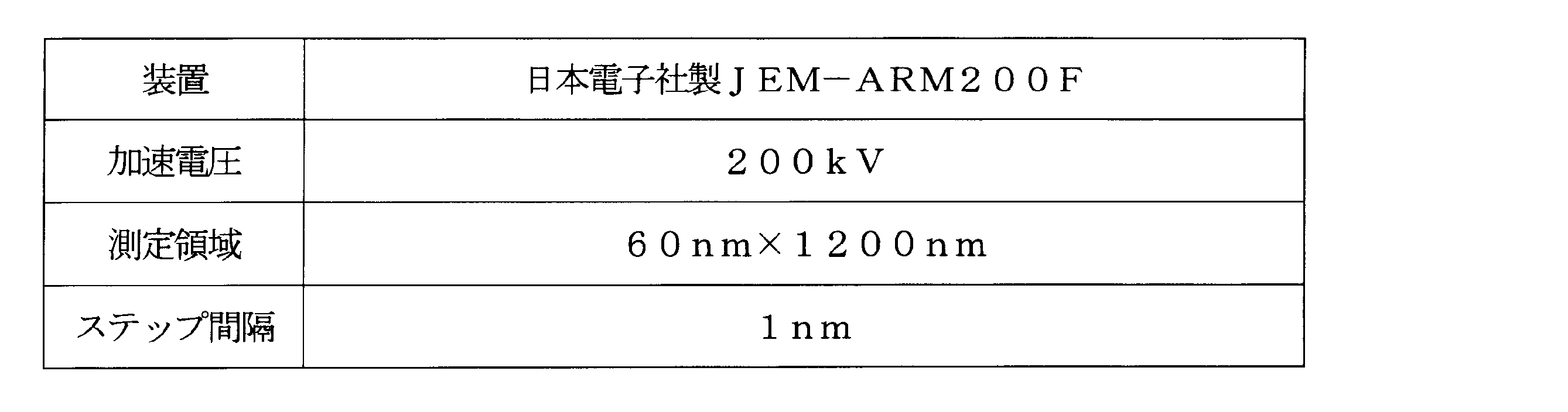
[2-1.逆極点図]
図14は、実施例サンプルの酸化物半導体層(Poly-OS膜)の逆極点図である。図14には、ND、TD、およびRDのそれぞれにおける逆極点図が示されている。ND、TD、およびRDのそれぞれにおける逆極点図は、図14に示された指標の値に従って、結晶方位の割合が増加する(例えば、指標はカラーキーでもよく、青色から赤色になる(可視光の波長が大きくなる)と結晶方位の割合が増加する。)。ND、TD、およびRDのいずれにおいても、大きな値を有する領域(領域A1、領域A2、および領域A3)が存在し、割合の大きい特定の結晶方位が存在することがわかった。例えば、酸化物半導体層の膜厚方向に対応するRDにおいては、結晶方位<001>および結晶方位<101>より結晶方位<111>の占める割合が大きい。
[2-1. Inverse pole figures]
FIG. 14 is an inverse pole figure of the oxide semiconductor layer (Poly-OS film) of the example sample. FIG. 14 shows inverse pole figures for ND, TD, and RD. In the inverse pole figures for ND, TD, and RD, the proportion of the crystal orientation increases according to the value of the index shown in FIG. 14 (for example, the index may be a color key, and the proportion of the crystal orientation increases as the color changes from blue to red (the wavelength of visible light increases)). In each of ND, TD, and RD, there are regions (regions A1, A2, and A3) having large values, and it was found that there are specific crystal orientations with a large proportion. For example, in RD corresponding to the film thickness direction of the oxide semiconductor layer, the proportion of the crystal orientation <111> is larger than that of the crystal orientation <001> and the crystal orientation <101>.
[2-2.IPFマップ]
図15は、実施例サンプルの酸化物半導体層(Poly-OS膜)のIPFマップである。図15には、ND、TD、およびRDのそれぞれにおけるIPFマップが示されている。図15では、図中の指標に従い、結晶方位<001>、結晶方位<101>、結晶方位<111>、および結晶方位<011>が、区分されている。
[2-2. IPF map]
15 is an IPF map of an oxide semiconductor layer (Poly-OS film) of an example sample. IPF maps for ND, TD, and RD are shown in Fig. 15. In Fig. 15, the crystal orientation <001>, the crystal orientation <101>, the crystal orientation <111>, and the crystal orientation <011> are classified according to the indexes in the figure.
図15に示す領域B1および領域B2において、結晶方位が不連続的に大きく変化していた。結晶方位の不連続的な変化は結晶粒界に相当し、領域B1および領域B2において、酸化物半導体層の上面から下面に(または、下面から上面に)向かって形成された結晶粒界が確認された。領域B1における結晶粒界と領域B2における結晶粒界との間における1つの結晶粒の結晶粒長は1080nmであった。また、1つの結晶粒が、酸化物半導体層の上面の一部および下面の一部を形成していた。すなわち、結晶粒長は、酸化物半導体層の膜厚の10倍以上であった。 In regions B1 and B2 shown in FIG. 15, the crystal orientation changed significantly and discontinuously. The discontinuous change in crystal orientation corresponds to a grain boundary, and in regions B1 and B2, a grain boundary was confirmed to have formed from the top surface to the bottom surface (or from the bottom surface to the top surface) of the oxide semiconductor layer. The grain length of one crystal grain between the grain boundary in region B1 and the grain boundary in region B2 was 1080 nm. In addition, one crystal grain formed part of the top surface and part of the bottom surface of the oxide semiconductor layer. In other words, the grain length was 10 times or more the thickness of the oxide semiconductor layer.
IPFマップにおける結晶粒内の結晶方位は、上述した逆極点図における結晶方位の割合と対応していた。例えば、RDにおける結晶粒の主な結晶方位は、結晶方位<111>である。 The crystal orientations within the grains in the IPF map corresponded to the proportion of crystal orientations in the inverse pole figures described above. For example, the main crystal orientation of the grains in the RD is the crystal orientation <111>.
領域B2における結晶粒界は、酸化物半導体層の膜厚方向に沿って形成されておらず、酸化物半導体層の膜厚方向から大きくずれていた。すなわち、領域B2における結晶粒界を挟んで隣接する2つの結晶粒は、酸化物半導体層の膜厚方向において互いに重畳していた。酸化物半導体層の膜厚方向と直交する方向において、隣接する2つの結晶粒の重畳する距離は34nmであった。 The grain boundary in region B2 was not formed along the film thickness direction of the oxide semiconductor layer, but was significantly shifted from the film thickness direction of the oxide semiconductor layer. In other words, two adjacent crystal grains sandwiching the grain boundary in region B2 overlapped each other in the film thickness direction of the oxide semiconductor layer. In the direction perpendicular to the film thickness direction of the oxide semiconductor layer, the overlap distance of two adjacent crystal grains was 34 nm.
なお、図示しないが、TEM像においても、領域B1および領域B2において結晶粒界を確認することができた。 Although not shown, grain boundaries could also be confirmed in the TEM image in areas B1 and B2.
[2-3.KAM値]
図16は、実施例サンプルの酸化物半導体層(Poly-OS膜)のKAMマップである。具体的には、図16には、測定領域内における測定点の各々のKAM値が、図16に示された指標の値に従って区分されている(例えば、指標はカラーキーでもよく、青色から赤色になる(可視光の波長が大きくなる)に従って、KAM値が0°から5°に増加する。)。なお、隣接する2つの測定点における結晶方位差が5°を超えると、結晶粒界とみなされるため、KAM値の上限は5°である。また、図17は、実施例サンプルの酸化物半導体層(Poly-OS膜)のKAM値の分布を表すグラフである。
[2-3. KAM value]
16 is a KAM map of the oxide semiconductor layer (Poly-OS film) of the example sample. Specifically, in FIG. 16, the KAM values of the measurement points in the measurement region are classified according to the values of the indices shown in FIG. 16 (for example, the indices may be a color key, and the KAM value increases from 0° to 5° as the color changes from blue to red (the wavelength of visible light increases)). Note that when the crystal orientation difference between two adjacent measurement points exceeds 5°, it is regarded as a grain boundary, and therefore the upper limit of the KAM value is 5°. FIG. 17 is a graph showing the distribution of the KAM values of the oxide semiconductor layer (Poly-OS film) of the example sample.
図16に示すように、酸化物半導体層には、0°近傍のKAM値を有する領域(カラーキーでは青色で示される領域に対応するため、以下では、説明の便宜上、「青色の領域」という。)だけでなく、0°近傍以外のKAM値を有する領域(カラーキーでは緑色で示される領域に対応するため、以下では、説明の便宜上、「緑色の領域」という。)も広く分布していた。全体的な傾向として、酸化物半導体層の中央部に青色の領域が広がり、酸化物半導体層の表面近傍(上端部および下端部の近傍)に緑色の領域が広がっていた。図17から理解されるように、0°近傍のKAM値を有する測定点だけでなく、0°近傍以外のKAM値を有する測定点も多く存在することがわかる。全ての測定点のKAM値を用いて算出されたKAM値の総平均値(KAMAVE(total))は、0.646°であった。また、KAM値の標準偏差(σ)は、0.396であった。なお、ステップ間隔を2nmにした場合、KAM値の総平均値(KAMAVE(total))は、0.670°であった。すなわち、ステップ間隔が増加すると、KAM値の総平均値(KAMAVE(total))が大きくなった。 As shown in FIG. 16, the oxide semiconductor layer has not only a region having a KAM value near 0° (corresponding to the region shown in blue in the color key, hereinafter, for convenience of explanation, it will be referred to as the "blue region"), but also a region having a KAM value other than near 0° (corresponding to the region shown in green in the color key, hereinafter, for convenience of explanation, it will be referred to as the "green region"). As an overall tendency, the blue region spread in the center of the oxide semiconductor layer, and the green region spread near the surface (near the upper end and the lower end) of the oxide semiconductor layer. As can be seen from FIG. 17, it can be seen that there are not only measurement points having a KAM value near 0°, but also many measurement points having a KAM value other than near 0°. The total average value of the KAM values (KAM AVE(total) ) calculated using the KAM values of all the measurement points was 0.646°. In addition, the standard deviation (σ) of the KAM value was 0.396. When the step interval was 2 nm, the total average value of the KAM values (KAM AVE(total) ) was 0.670°. That is, as the step interval increased, the total average value of the KAM values (KAM AVE(total) ) increased.
TEM-EDマッピング法は、微小領域における測定であるが、Poly-OS膜の場合、このような微小領域においてもKAM値の総平均値および標準偏差が大きい。これは、Poly-OS膜の結晶粒内における結晶方位の変化が大きいことを意味する。Poly-OS膜に含まれる結晶粒は、大きな結晶粒長(または結晶粒径)を有するにもかかわらず、局所的な結晶方位の変化が大きい。これは、従来の多結晶構造を有する酸化物半導体膜では見られないPoly-OS膜の特徴の1つである。 The TEM-ED mapping method is a measurement in a microscopic area, but in the case of the Poly-OS film, the total average value and standard deviation of the KAM value are large even in such a microscopic area. This means that there is a large change in the crystal orientation within the crystal grains of the Poly-OS film. Although the crystal grains contained in the Poly-OS film have a large crystal grain length (or crystal grain size), there is a large change in the local crystal orientation. This is one of the characteristics of the Poly-OS film that is not seen in conventional oxide semiconductor films having a polycrystalline structure.
図18は、実施例サンプルの酸化物半導体層(Poly-OS膜)におけるKAM値の深さ平均値を表すグラフである。上述したように、酸化物半導体層の中央部と表面近傍(上端部および下端部の近傍)とでは、KAM値の分布に違いが見られた。そこで、ゲート絶縁層と酸化物半導体層との界面からの距離(酸化物半導体層の深さ)ごとに、測定点のKAM値を集計し、その平均値であるKAM値の深さ平均値(KAMAVE(depth))を算出した。KAM値の深さ平均値(KAMAVE(depth))は、酸化物半導体層の深さに応じて区分された一部の測定点のKAM値の平均値である。なお、酸化物半導体層の表面の凹凸の影響を除外するため、区分された領域内に含まれる測定点の数が、中央部の測定点の数の90%以上である領域を有効な領域として、酸化物半導体層のKAM値の深さ平均値(KAMAVE(depth))を算出した。図18に示すグラフは、酸化物半導体層の膜厚方向に対するKAM値の深さ平均値(KAMAVE(depth))がプロットされている。 FIG. 18 is a graph showing the depth average value of the KAM value in the oxide semiconductor layer (Poly-OS film) of the example sample. As described above, a difference was observed in the distribution of the KAM value between the center part and the surface vicinity (near the upper end and the lower end) of the oxide semiconductor layer. Therefore, the KAM values of the measurement points were collected for each distance from the interface between the gate insulating layer and the oxide semiconductor layer (depth of the oxide semiconductor layer), and the depth average value of the KAM value (KAM AVE(depth) ) was calculated, which is the average value. The depth average value of the KAM value (KAM AVE(depth) ) is the average value of the KAM values of some measurement points divided according to the depth of the oxide semiconductor layer. In order to exclude the influence of the unevenness of the surface of the oxide semiconductor layer, a region in which the number of measurement points included in the divided region is 90% or more of the number of measurement points in the center part was set as a valid region, and the depth average value of the KAM value (KAM AVE(depth) ) of the oxide semiconductor layer was calculated. In the graph shown in FIG. 18, the depth average value of the KAM value (KAM AVE(depth) ) is plotted against the thickness direction of the oxide semiconductor layer.
図18に示すように、酸化物半導体層の中央部よりも、酸化物半導体層とゲート絶縁層との界面に近い上端部および酸化物半導体層と金属酸化物層との界面に近い下端部の方がKAM値の深さ平均値(KAMAVE(depth))が大きかった。中央部(深さ15nm)、上端部(深さ0nm)、および下端部(深さ32nm)のKAM値の深さ平均値(KAMAVE(depth))は、それぞれ、0.554°、0.828°、および0.802°であった。KAM値の深さ平均値(KAMAVE(depth))における、上端部と中央部との差、および下端部と中央部との差は、0.2°以上であった。
As shown in FIG. 18, the average depth value of the KAM value (KAM AVE(depth)) was larger at the upper end portion near the interface between the oxide semiconductor layer and the gate insulating layer and at the lower end portion near the interface between the oxide semiconductor layer and the metal oxide layer than at the central portion of the oxide semiconductor layer. The average depth values of the KAM value (KAM AVE(depth) ) at the central portion (
上述の結果は、酸化物半導体層の界面近傍における結晶方位の変化が大きいことを示す。Poly-OS膜では、膜厚方向においても、局所的な結晶方位の変化が大きい。従来の多結晶構造を有する酸化物半導体膜では、結晶粒内における歪みが緩和されるように結晶粒長(または結晶粒径)が小さくなり、酸化物半導体膜の上面から下面までを1つの結晶粒で形成することは困難である。一方、Poly-OS膜では、結晶方位の変化の大きな1つの結晶粒によって、上面から下面までを形成することが可能である。これは、従来の多結晶構造を有する酸化物半導体膜では見られないPoly-OS膜の特徴の1つである。 The above results indicate that there is a large change in crystal orientation near the interface of the oxide semiconductor layer. In the Poly-OS film, the local change in crystal orientation is also large in the film thickness direction. In a conventional oxide semiconductor film having a polycrystalline structure, the crystal grain length (or crystal grain size) is small so that the distortion in the crystal grains is relieved, and it is difficult to form the oxide semiconductor film from the top to the bottom with a single crystal grain. On the other hand, in the Poly-OS film, it is possible to form the oxide semiconductor film from the top to the bottom with a single crystal grain that has a large change in crystal orientation. This is one of the characteristics of the Poly-OS film that is not seen in a conventional oxide semiconductor film having a polycrystalline structure.
[3.電気特性]
作製された薄膜トランジスタの電気特性を測定した。電気特性から算出された電界効果移動度は33.5cm2/Vsであった。薄膜トランジスタのチャネルとしてPoly-OS膜を用いると、30cm2/Vsを超える電界効果移動度(飽和領域における電界効果移動度)が得られることがわかった。
3. Electrical Characteristics
The electrical characteristics of the fabricated thin film transistor were measured. The field effect mobility calculated from the electrical characteristics was 33.5 cm 2 /Vs. It was found that when a Poly-OS film was used as a channel of a thin film transistor, a field effect mobility (field effect mobility in a saturated region) of more than 30 cm 2 /Vs could be obtained.
本発明の実施形態として上述した各実施形態は、相互に矛盾しない限りにおいて、適宜組み合わせて実施することができる。また、各実施形態を基にして、当業者が適宜構成要素の追加、削除、もしくは設計変更を行ったもの、または工程の追加、省略、もしくは条件変更を行ったものも、本発明の要旨を備えている限り、本発明の範囲に含まれる。 The above-described embodiments of the present invention may be combined as appropriate to the extent that they are not mutually inconsistent. Furthermore, if a person skilled in the art adds or removes components or modifies the design based on each embodiment, or adds or omits processes or modifies conditions, these are also included in the scope of the present invention as long as they incorporate the essence of the present invention.
上述した各実施形態の態様によりもたらされる作用効果とは異なる他の作用効果であっても、本明細書の記載から明らかなもの、または当業者において容易に予測し得るものについては、当然に本発明によりもたらされるものと解される。 Even if there are other effects and advantages different from those brought about by the aspects of each of the above-mentioned embodiments, if they are clear from the description in this specification or can be easily predicted by a person skilled in the art, they are naturally understood to be brought about by the present invention.
10:薄膜トランジスタ、 100:基板、 105:遮光層、 110:第1の絶縁層、 120:第2の絶縁層、 130:金属酸化物層、 135:金属酸化物膜、 140:酸化物半導体層、 145:酸化物半導体膜、 150:ゲート絶縁層、 160:ゲート電極、 170:第3の絶縁層、 171:開口、 173:開口、 180:第4の絶縁層、 200:ソース・ドレイン電極、 201:ソース電極、 203:ドレイン電極、 500:TEM試料、 1000:電子機器、 1100:表示装置 10: Thin film transistor, 100: Substrate, 105: Light shielding layer, 110: First insulating layer, 120: Second insulating layer, 130: Metal oxide layer, 135: Metal oxide film, 140: Oxide semiconductor layer, 145: Oxide semiconductor film, 150: Gate insulating layer, 160: Gate electrode, 170: Third insulating layer, 171: Opening, 173: Opening, 180: Fourth insulating layer, 200: Source/drain electrode, 201: Source electrode, 203: Drain electrode, 500: TEM sample, 1000: Electronic device, 1100: Display device
Claims (17)
前記基板の上に設けられた金属酸化物層と、
前記金属酸化物層と接して設けられる、複数の結晶粒を含む酸化物半導体層と、
前記酸化物半導体層の上に設けられたゲート電極と、
前記酸化物半導体層と前記ゲート電極との間に設けられたゲート絶縁層と、を含み、
前記酸化物半導体層の膜厚方向と交差する方向から照射される電子線が前記酸化物半導体層を透過して得られる電子回折パターンに基づいて前記酸化物半導体層の複数の測定点の各々における結晶方位が取得されるとき、前記複数の測定点において算出されるKAM値の平均値が0.6°以上である、薄膜トランジスタ。 A substrate;
a metal oxide layer provided on the substrate;
an oxide semiconductor layer including a plurality of crystal grains provided in contact with the metal oxide layer;
a gate electrode provided on the oxide semiconductor layer;
a gate insulating layer provided between the oxide semiconductor layer and the gate electrode;
a thin film transistor, wherein when a crystal orientation at each of a plurality of measurement points of the oxide semiconductor layer is obtained based on an electron diffraction pattern obtained by transmitting an electron beam irradiated from a direction intersecting a film thickness direction of the oxide semiconductor layer through the oxide semiconductor layer, an average value of KAM values calculated at the plurality of measurement points is 0.6° or more.
前記所定のステップ間隔は、1nm以上である、請求項1に記載の薄膜トランジスタ。 the electron diffraction pattern at each of the plurality of measurement points is observed at predetermined step intervals;
The thin film transistor of claim 1 , wherein the predetermined step spacing is 1 nm or greater.
前記酸化物半導体層の前記膜厚方向と交差する前記方向において、前記隣接する2つの結晶粒の重畳する距離は、10nm以上である、請求項1に記載の薄膜トランジスタ。 two crystal grains adjacent to each other across a crystal grain boundary overlap each other in the film thickness direction of the oxide semiconductor layer;
The thin film transistor according to claim 1 , wherein an overlapping distance between the two adjacent crystal grains in the direction intersecting the thickness direction of the oxide semiconductor layer is 10 nm or more.
インジウムと、
前記インジウムを除く、少なくとも1つ以上の金属元素と、を含み、
前記インジウムおよび前記少なくとも1つ以上の金属元素に対する前記インジウムの比率は、50%以上である、請求項1に記載の薄膜トランジスタ。 The oxide semiconductor layer is
Indium,
At least one metal element other than indium;
The thin film transistor of claim 1 , wherein the indium and the ratio of the indium to the at least one or more metal elements is 50% or more.
17. An electronic device comprising the thin film transistor according to claim 1.
Priority Applications (5)
| Application Number | Priority Date | Filing Date | Title |
|---|---|---|---|
| KR1020257022126A KR20250117810A (en) | 2023-03-17 | 2024-03-12 | Thin film transistors and electronic devices |
| CN202480006547.4A CN120570087A (en) | 2023-03-17 | 2024-03-12 | Thin film transistor and electronic device |
| JP2025508339A JPWO2024195629A1 (en) | 2023-03-17 | 2024-03-12 | |
| DE112024000552.7T DE112024000552T5 (en) | 2023-03-17 | 2024-03-12 | THIN-LAYER TRANSISTOR AND ELECTRONIC DEVICE |
| US19/319,774 US20260006849A1 (en) | 2023-03-17 | 2025-09-05 | Thin film transistor and electronic device |
Applications Claiming Priority (2)
| Application Number | Priority Date | Filing Date | Title |
|---|---|---|---|
| JP2023-043065 | 2023-03-17 | ||
| JP2023043065 | 2023-03-17 |
Related Child Applications (1)
| Application Number | Title | Priority Date | Filing Date |
|---|---|---|---|
| US19/319,774 Continuation US20260006849A1 (en) | 2023-03-17 | 2025-09-05 | Thin film transistor and electronic device |
Publications (1)
| Publication Number | Publication Date |
|---|---|
| WO2024195629A1 true WO2024195629A1 (en) | 2024-09-26 |
Family
ID=92842100
Family Applications (1)
| Application Number | Title | Priority Date | Filing Date |
|---|---|---|---|
| PCT/JP2024/009575 Ceased WO2024195629A1 (en) | 2023-03-17 | 2024-03-12 | Thin-film transistor and electronic device |
Country Status (7)
| Country | Link |
|---|---|
| US (1) | US20260006849A1 (en) |
| JP (1) | JPWO2024195629A1 (en) |
| KR (1) | KR20250117810A (en) |
| CN (1) | CN120570087A (en) |
| DE (1) | DE112024000552T5 (en) |
| TW (1) | TWI899892B (en) |
| WO (1) | WO2024195629A1 (en) |
Citations (3)
| Publication number | Priority date | Publication date | Assignee | Title |
|---|---|---|---|---|
| JP2012253315A (en) * | 2010-12-28 | 2012-12-20 | Idemitsu Kosan Co Ltd | Laminate structure having oxide semiconductor thin film layer, and thin film transistor |
| JP2015173259A (en) * | 2014-02-19 | 2015-10-01 | 株式会社半導体エネルギー研究所 | Oxide, semiconductor device, module and electronic apparatus |
| JP2016180178A (en) * | 2015-03-13 | 2016-10-13 | 株式会社半導体エネルギー研究所 | Oxide and production method thereof |
Family Cites Families (9)
| Publication number | Priority date | Publication date | Assignee | Title |
|---|---|---|---|---|
| JP2003273016A (en) * | 2002-01-11 | 2003-09-26 | Sharp Corp | Semiconductor film and method for forming the same, and semiconductor device and display device using the semiconductor film. |
| US8871565B2 (en) | 2010-09-13 | 2014-10-28 | Semiconductor Energy Laboratory Co., Ltd. | Method for manufacturing semiconductor device |
| EP2880690B1 (en) | 2012-08-03 | 2019-02-27 | Semiconductor Energy Laboratory Co. Ltd. | Semiconductor device with oxide semiconductor stacked film |
| TWI761605B (en) | 2012-09-14 | 2022-04-21 | 日商半導體能源研究所股份有限公司 | Semiconductor device and method for fabricating the same |
| KR102220279B1 (en) | 2012-10-19 | 2021-02-24 | 가부시키가이샤 한도오따이 에네루기 켄큐쇼 | Method for forming multilayer film including oxide semiconductor film and method for manufacturing semiconductor device |
| US9425217B2 (en) | 2013-09-23 | 2016-08-23 | Semiconductor Energy Laboratory Co., Ltd. | Semiconductor device |
| US9368582B2 (en) * | 2013-11-04 | 2016-06-14 | Avogy, Inc. | High power gallium nitride electronics using miscut substrates |
| WO2017137869A1 (en) | 2016-02-12 | 2017-08-17 | Semiconductor Energy Laboratory Co., Ltd. | Semiconductor device and display device including the semiconductor device |
| JP7647871B2 (en) * | 2021-03-26 | 2025-03-18 | 三菱マテリアル株式会社 | Metal plate material, laminate, and insulated circuit board |
-
2024
- 2024-03-12 WO PCT/JP2024/009575 patent/WO2024195629A1/en not_active Ceased
- 2024-03-12 DE DE112024000552.7T patent/DE112024000552T5/en active Pending
- 2024-03-12 CN CN202480006547.4A patent/CN120570087A/en active Pending
- 2024-03-12 JP JP2025508339A patent/JPWO2024195629A1/ja active Pending
- 2024-03-12 KR KR1020257022126A patent/KR20250117810A/en active Pending
- 2024-03-15 TW TW113109602A patent/TWI899892B/en active
-
2025
- 2025-09-05 US US19/319,774 patent/US20260006849A1/en active Pending
Patent Citations (3)
| Publication number | Priority date | Publication date | Assignee | Title |
|---|---|---|---|---|
| JP2012253315A (en) * | 2010-12-28 | 2012-12-20 | Idemitsu Kosan Co Ltd | Laminate structure having oxide semiconductor thin film layer, and thin film transistor |
| JP2015173259A (en) * | 2014-02-19 | 2015-10-01 | 株式会社半導体エネルギー研究所 | Oxide, semiconductor device, module and electronic apparatus |
| JP2016180178A (en) * | 2015-03-13 | 2016-10-13 | 株式会社半導体エネルギー研究所 | Oxide and production method thereof |
Also Published As
| Publication number | Publication date |
|---|---|
| TWI899892B (en) | 2025-10-01 |
| DE112024000552T5 (en) | 2025-12-11 |
| TW202439617A (en) | 2024-10-01 |
| JPWO2024195629A1 (en) | 2024-09-26 |
| CN120570087A (en) | 2025-08-29 |
| KR20250117810A (en) | 2025-08-05 |
| US20260006849A1 (en) | 2026-01-01 |
Similar Documents
| Publication | Publication Date | Title |
|---|---|---|
| US20250176237A1 (en) | Oxide semiconductor film, thin film transistor, and electronic device | |
| US20250176219A1 (en) | Thin film transistor and electronic device | |
| WO2024195629A1 (en) | Thin-film transistor and electronic device | |
| US20250393248A1 (en) | Thin film transistor and electronic device | |
| WO2025069956A1 (en) | Thin-film transistor and electronic device | |
| WO2025069957A1 (en) | Oxide semiconductor film, thin-film transistor, and electronic device | |
| TWI899894B (en) | Oxide semiconductor film, multilayer structure, thin film transistor, and electronic device | |
| US20260006848A1 (en) | Oxide semiconductor film, thin film transistor, and electronic device | |
| US20250176222A1 (en) | Oxide semiconductor film, thin film transistor, and electronic device | |
| US20250331259A1 (en) | Laminated structure, thin film transistor, and electronic device | |
| TWI911559B (en) | Oxide semiconductor films, thin-film transistors, and electronic devices | |
| US20250015196A1 (en) | Thin film transistor and electronic device | |
| US20250015198A1 (en) | Oxide semiconductor film, thin film transistor, and electronic device |
Legal Events
| Date | Code | Title | Description |
|---|---|---|---|
| 121 | Ep: the epo has been informed by wipo that ep was designated in this application |
Ref document number: 24774768 Country of ref document: EP Kind code of ref document: A1 |
|
| WWE | Wipo information: entry into national phase |
Ref document number: 1020257022126 Country of ref document: KR Ref document number: 202480006547.4 Country of ref document: CN |
|
| ENP | Entry into the national phase |
Ref document number: 2025508339 Country of ref document: JP Kind code of ref document: A |
|
| WWE | Wipo information: entry into national phase |
Ref document number: 2025508339 Country of ref document: JP |
|
| WWP | Wipo information: published in national office |
Ref document number: 1020257022126 Country of ref document: KR |
|
| WWP | Wipo information: published in national office |
Ref document number: 202480006547.4 Country of ref document: CN |
|
| WWE | Wipo information: entry into national phase |
Ref document number: 112024000552 Country of ref document: DE |
|
| WWP | Wipo information: published in national office |
Ref document number: 112024000552 Country of ref document: DE |