WO2024129781A1 - Feature fill using inhibition - Google Patents
Feature fill using inhibition Download PDFInfo
- Publication number
- WO2024129781A1 WO2024129781A1 PCT/US2023/083696 US2023083696W WO2024129781A1 WO 2024129781 A1 WO2024129781 A1 WO 2024129781A1 US 2023083696 W US2023083696 W US 2023083696W WO 2024129781 A1 WO2024129781 A1 WO 2024129781A1
- Authority
- WO
- WIPO (PCT)
- Prior art keywords
- feature
- metal
- deposition
- nitrogen
- reducing agent
- Prior art date
- Legal status (The legal status is an assumption and is not a legal conclusion. Google has not performed a legal analysis and makes no representation as to the accuracy of the status listed.)
- Ceased
Links
Classifications
-
- C—CHEMISTRY; METALLURGY
- C23—COATING METALLIC MATERIAL; COATING MATERIAL WITH METALLIC MATERIAL; CHEMICAL SURFACE TREATMENT; DIFFUSION TREATMENT OF METALLIC MATERIAL; COATING BY VACUUM EVAPORATION, BY SPUTTERING, BY ION IMPLANTATION OR BY CHEMICAL VAPOUR DEPOSITION, IN GENERAL; INHIBITING CORROSION OF METALLIC MATERIAL OR INCRUSTATION IN GENERAL
- C23C—COATING METALLIC MATERIAL; COATING MATERIAL WITH METALLIC MATERIAL; SURFACE TREATMENT OF METALLIC MATERIAL BY DIFFUSION INTO THE SURFACE, BY CHEMICAL CONVERSION OR SUBSTITUTION; COATING BY VACUUM EVAPORATION, BY SPUTTERING, BY ION IMPLANTATION OR BY CHEMICAL VAPOUR DEPOSITION, IN GENERAL
- C23C16/00—Chemical coating by decomposition of gaseous compounds, without leaving reaction products of surface material in the coating, i.e. chemical vapour deposition [CVD] processes
- C23C16/04—Coating on selected surface areas, e.g. using masks
- C23C16/045—Coating cavities or hollow spaces, e.g. interior of tubes; Infiltration of porous substrates
-
- C—CHEMISTRY; METALLURGY
- C23—COATING METALLIC MATERIAL; COATING MATERIAL WITH METALLIC MATERIAL; CHEMICAL SURFACE TREATMENT; DIFFUSION TREATMENT OF METALLIC MATERIAL; COATING BY VACUUM EVAPORATION, BY SPUTTERING, BY ION IMPLANTATION OR BY CHEMICAL VAPOUR DEPOSITION, IN GENERAL; INHIBITING CORROSION OF METALLIC MATERIAL OR INCRUSTATION IN GENERAL
- C23C—COATING METALLIC MATERIAL; COATING MATERIAL WITH METALLIC MATERIAL; SURFACE TREATMENT OF METALLIC MATERIAL BY DIFFUSION INTO THE SURFACE, BY CHEMICAL CONVERSION OR SUBSTITUTION; COATING BY VACUUM EVAPORATION, BY SPUTTERING, BY ION IMPLANTATION OR BY CHEMICAL VAPOUR DEPOSITION, IN GENERAL
- C23C16/00—Chemical coating by decomposition of gaseous compounds, without leaving reaction products of surface material in the coating, i.e. chemical vapour deposition [CVD] processes
- C23C16/02—Pretreatment of the material to be coated
- C23C16/0272—Deposition of sub-layers, e.g. to promote the adhesion of the main coating
- C23C16/0281—Deposition of sub-layers, e.g. to promote the adhesion of the main coating of metallic sub-layers
-
- C—CHEMISTRY; METALLURGY
- C23—COATING METALLIC MATERIAL; COATING MATERIAL WITH METALLIC MATERIAL; CHEMICAL SURFACE TREATMENT; DIFFUSION TREATMENT OF METALLIC MATERIAL; COATING BY VACUUM EVAPORATION, BY SPUTTERING, BY ION IMPLANTATION OR BY CHEMICAL VAPOUR DEPOSITION, IN GENERAL; INHIBITING CORROSION OF METALLIC MATERIAL OR INCRUSTATION IN GENERAL
- C23C—COATING METALLIC MATERIAL; COATING MATERIAL WITH METALLIC MATERIAL; SURFACE TREATMENT OF METALLIC MATERIAL BY DIFFUSION INTO THE SURFACE, BY CHEMICAL CONVERSION OR SUBSTITUTION; COATING BY VACUUM EVAPORATION, BY SPUTTERING, BY ION IMPLANTATION OR BY CHEMICAL VAPOUR DEPOSITION, IN GENERAL
- C23C16/00—Chemical coating by decomposition of gaseous compounds, without leaving reaction products of surface material in the coating, i.e. chemical vapour deposition [CVD] processes
- C23C16/06—Chemical coating by decomposition of gaseous compounds, without leaving reaction products of surface material in the coating, i.e. chemical vapour deposition [CVD] processes characterised by the deposition of metallic material
- C23C16/08—Chemical coating by decomposition of gaseous compounds, without leaving reaction products of surface material in the coating, i.e. chemical vapour deposition [CVD] processes characterised by the deposition of metallic material from metal halides
- C23C16/14—Deposition of only one other metal element
-
- C—CHEMISTRY; METALLURGY
- C23—COATING METALLIC MATERIAL; COATING MATERIAL WITH METALLIC MATERIAL; CHEMICAL SURFACE TREATMENT; DIFFUSION TREATMENT OF METALLIC MATERIAL; COATING BY VACUUM EVAPORATION, BY SPUTTERING, BY ION IMPLANTATION OR BY CHEMICAL VAPOUR DEPOSITION, IN GENERAL; INHIBITING CORROSION OF METALLIC MATERIAL OR INCRUSTATION IN GENERAL
- C23C—COATING METALLIC MATERIAL; COATING MATERIAL WITH METALLIC MATERIAL; SURFACE TREATMENT OF METALLIC MATERIAL BY DIFFUSION INTO THE SURFACE, BY CHEMICAL CONVERSION OR SUBSTITUTION; COATING BY VACUUM EVAPORATION, BY SPUTTERING, BY ION IMPLANTATION OR BY CHEMICAL VAPOUR DEPOSITION, IN GENERAL
- C23C16/00—Chemical coating by decomposition of gaseous compounds, without leaving reaction products of surface material in the coating, i.e. chemical vapour deposition [CVD] processes
- C23C16/44—Chemical coating by decomposition of gaseous compounds, without leaving reaction products of surface material in the coating, i.e. chemical vapour deposition [CVD] processes characterised by the method of coating
- C23C16/455—Chemical coating by decomposition of gaseous compounds, without leaving reaction products of surface material in the coating, i.e. chemical vapour deposition [CVD] processes characterised by the method of coating characterised by the method used for introducing gases into reaction chamber or for modifying gas flows in reaction chamber
- C23C16/45523—Pulsed gas flow or change of composition over time
- C23C16/45525—Atomic layer deposition [ALD]
- C23C16/45527—Atomic layer deposition [ALD] characterized by the ALD cycle, e.g. different flows or temperatures during half-reactions, unusual pulsing sequence, use of precursor mixtures or auxiliary reactants or activations
- C23C16/45534—Use of auxiliary reactants other than used for contributing to the composition of the main film, e.g. catalysts, activators or scavengers
-
- C—CHEMISTRY; METALLURGY
- C23—COATING METALLIC MATERIAL; COATING MATERIAL WITH METALLIC MATERIAL; CHEMICAL SURFACE TREATMENT; DIFFUSION TREATMENT OF METALLIC MATERIAL; COATING BY VACUUM EVAPORATION, BY SPUTTERING, BY ION IMPLANTATION OR BY CHEMICAL VAPOUR DEPOSITION, IN GENERAL; INHIBITING CORROSION OF METALLIC MATERIAL OR INCRUSTATION IN GENERAL
- C23C—COATING METALLIC MATERIAL; COATING MATERIAL WITH METALLIC MATERIAL; SURFACE TREATMENT OF METALLIC MATERIAL BY DIFFUSION INTO THE SURFACE, BY CHEMICAL CONVERSION OR SUBSTITUTION; COATING BY VACUUM EVAPORATION, BY SPUTTERING, BY ION IMPLANTATION OR BY CHEMICAL VAPOUR DEPOSITION, IN GENERAL
- C23C16/00—Chemical coating by decomposition of gaseous compounds, without leaving reaction products of surface material in the coating, i.e. chemical vapour deposition [CVD] processes
- C23C16/44—Chemical coating by decomposition of gaseous compounds, without leaving reaction products of surface material in the coating, i.e. chemical vapour deposition [CVD] processes characterised by the method of coating
- C23C16/455—Chemical coating by decomposition of gaseous compounds, without leaving reaction products of surface material in the coating, i.e. chemical vapour deposition [CVD] processes characterised by the method of coating characterised by the method used for introducing gases into reaction chamber or for modifying gas flows in reaction chamber
- C23C16/45523—Pulsed gas flow or change of composition over time
- C23C16/45525—Atomic layer deposition [ALD]
- C23C16/45553—Atomic layer deposition [ALD] characterized by the use of precursors specially adapted for ALD
-
- C—CHEMISTRY; METALLURGY
- C23—COATING METALLIC MATERIAL; COATING MATERIAL WITH METALLIC MATERIAL; CHEMICAL SURFACE TREATMENT; DIFFUSION TREATMENT OF METALLIC MATERIAL; COATING BY VACUUM EVAPORATION, BY SPUTTERING, BY ION IMPLANTATION OR BY CHEMICAL VAPOUR DEPOSITION, IN GENERAL; INHIBITING CORROSION OF METALLIC MATERIAL OR INCRUSTATION IN GENERAL
- C23C—COATING METALLIC MATERIAL; COATING MATERIAL WITH METALLIC MATERIAL; SURFACE TREATMENT OF METALLIC MATERIAL BY DIFFUSION INTO THE SURFACE, BY CHEMICAL CONVERSION OR SUBSTITUTION; COATING BY VACUUM EVAPORATION, BY SPUTTERING, BY ION IMPLANTATION OR BY CHEMICAL VAPOUR DEPOSITION, IN GENERAL
- C23C16/00—Chemical coating by decomposition of gaseous compounds, without leaving reaction products of surface material in the coating, i.e. chemical vapour deposition [CVD] processes
- C23C16/44—Chemical coating by decomposition of gaseous compounds, without leaving reaction products of surface material in the coating, i.e. chemical vapour deposition [CVD] processes characterised by the method of coating
- C23C16/455—Chemical coating by decomposition of gaseous compounds, without leaving reaction products of surface material in the coating, i.e. chemical vapour deposition [CVD] processes characterised by the method of coating characterised by the method used for introducing gases into reaction chamber or for modifying gas flows in reaction chamber
- C23C16/45563—Gas nozzles
- C23C16/45565—Shower nozzles
-
- C—CHEMISTRY; METALLURGY
- C23—COATING METALLIC MATERIAL; COATING MATERIAL WITH METALLIC MATERIAL; CHEMICAL SURFACE TREATMENT; DIFFUSION TREATMENT OF METALLIC MATERIAL; COATING BY VACUUM EVAPORATION, BY SPUTTERING, BY ION IMPLANTATION OR BY CHEMICAL VAPOUR DEPOSITION, IN GENERAL; INHIBITING CORROSION OF METALLIC MATERIAL OR INCRUSTATION IN GENERAL
- C23C—COATING METALLIC MATERIAL; COATING MATERIAL WITH METALLIC MATERIAL; SURFACE TREATMENT OF METALLIC MATERIAL BY DIFFUSION INTO THE SURFACE, BY CHEMICAL CONVERSION OR SUBSTITUTION; COATING BY VACUUM EVAPORATION, BY SPUTTERING, BY ION IMPLANTATION OR BY CHEMICAL VAPOUR DEPOSITION, IN GENERAL
- C23C16/00—Chemical coating by decomposition of gaseous compounds, without leaving reaction products of surface material in the coating, i.e. chemical vapour deposition [CVD] processes
- C23C16/44—Chemical coating by decomposition of gaseous compounds, without leaving reaction products of surface material in the coating, i.e. chemical vapour deposition [CVD] processes characterised by the method of coating
- C23C16/52—Controlling or regulating the coating process
-
- H10P14/43—
-
- H10W20/057—
Definitions
- Deposition of metals in features is an integral part of many semiconductor fabrication processes.
- the deposited metal films may be used for horizontal interconnects, vias between adjacent metal layers, and contacts between metal layers and devices.
- a tungsten (W) layer may be deposited on a titanium nitride (TiN) barrier layer to form a TiN/W bilayer by a chemical vapor deposition (CVD) process using tungsten hexafluoride (WFe).
- CVD chemical vapor deposition
- WFe tungsten hexafluoride
- One aspect of the disclosure relates to a method including: a) providing a feature to be filled with metal, the feature including a feature opening and sidewalls extending from the feature opening to a process station; and b) exposing the feature to a metal precursor, a reducing agent, and a nitrogen-containing gas to fill the feature with metal, wherein the nitrogen-containing gas inhibits metal deposition on surfaces of the sidewalls it contacts.
- a flow of the nitrogen-containing gas is decreased as more metal is deposited in the feature.
- the method further includes, prior to (b), forming a liner of metal in the feature.
- the method further includes, prior to (b), exposing the feature to the nitrogen-containing gas without significant deposition to inhibit deposition of the metal near the feature opening.
- (b) includes continuously co-flowing the metal precursor, the reducing agent, and the nitrogen-containing gas into the process station.
- the method further includes, prior to (b), exposing the feature to the nitrogen-containing gas without significant deposition to inhibit deposition of the metal near the feature opening.
- a flow of the reducing agent is ramped up and a flow of the nitrogen-containing gas is ramped down as (b) progresses.
- (b) includes continuously flowing the metal precursor into the process station while pulsing the reducing agent and the nitrogen-containing gas in alternating sequence.
- (b) includes continuously flowing the nitrogen-containing gas into the process station containing the substrate while pulsing the metal precursor and the reducing agent into the process station.
- the metal precursor and the reducing agent are pulsed together into the process station.
- pulses of the metal precursor and pulses of the reducing agent are alternated.
- (b) includes continuously flowing the reducing agent into the process station containing the substrate while pulsing the metal precursor and nitrogen-containing gas into the process station.
- the metal precursor and nitrogen-containing gas are pulsed together into the process station.
- pulses of the metal precursor and pulses of the nitrogencontaining gas are alternated.
- the metal is one of a tungsten (W), molybdenum (Mo), ruthenium (Ru), or cobalt (Co).
- the nitrogen-containing gas is ammonia.
- Another aspect of the disclosure relates to an apparatus including: a process station including a showerhead to direct gases to a substrate support; a controller configured to execute machine-readable instructions for filling a feature with metal, the instructions including instructions for: (a) causing flowing of a metal precursor, a reducing agent, and a nitrogen-containing gas into the process station to fill the feature with metal.
- the instructions for (a) cause continuous co-flowing of the metal precursor, the reducing agent, and the nitrogen-containing gas into the process station.
- the instructions further include instructions for, prior to (a), causing flowing of the nitrogen-containing gas without flowing of the reducing agent to inhibit metal deposition near the feature opening.
- the instructions further include instructions for causing ramping up of flowing of the reducing agent flow and ramping down of flowing of the nitrogen-containing gas as (a) progresses.
- Figures 1 A and IB are schematic examples of material stacks that include a conductive metal layer according to various embodiments.
- Figures 2A-2K are schematic examples of various structures into which a metal fill layer may be deposited in accordance with disclosed embodiments.
- Figure 3A is a process flow diagram illustrating operations in filling a structure with a metal according to various embodiments.
- Figure 3B shows a schematic of a cross-section of feature at various stages in according to an embodiment of the process in Figure 3 A.
- Figure 4 shows a schematic of a cross-section of feature at various stages of fill.
- Figure 5 shows an example of a process flow diagram illustrating operations in a method of filling a feature with metal.
- Figure 6 shows a schematic of a cross-section of feature at various stages in according to an embodiment of the process in Figure 5.
- Figures 7 and 8 illustrate examples of various ramped flow profiles.
- FIG. 9-11 shows schematics of apparatus that may be used in accordance with certain embodiments.
- the substrate 102 may be a silicon or other semiconductor wafer, e.g., a 200-mm wafer, a 300-mm wafer, or a 450-mm wafer, including wafers having one or more layers of material, such as dielectric, conducting, or semi-conducting material deposited thereon.
- the methods may also be applied to form metallization stack structures on other substrates, such as glass, plastic, and the like.
- a dielectric layer 104 is on the substrate 102.
- the dielectric layer 104 may be deposited directly on a semiconductor (e.g., silicon (Si)) surface of the substrate 102, or there may be any number of intervening layers.
- semiconductor e.g., silicon (Si)
- dielectric layers include doped and undoped silicon oxide (SiCh), silicon nitride, and aluminum oxide (AI2O3) layers, with specific examples including doped or undoped layers SiCh and AI2O3.
- a diffusion barrier layer 106 is disposed between the conductive metal layer 108 and the dielectric layer 104.
- diffusion barrier layers including titanium nitride (TiN), titanium/titanium nitride (Ti/TiN), tungsten nitride (WN), and tungsten carbon nitride (WCN). Further examples of diffusion barriers are multi-component Mo-containing films such as molybdenum nitride (MoN).
- the conductive metal layer 108 is the main conductor of the structure. In some embodiments, the conductive metal layer 108 may include multiple bulk layers deposited at different conditions. The conductive metal layer 108 may or may not include a nucleation layer, e.g., the conductive metal layer 108 may include a W bulk layer deposited on W nucleation layer.
- a metal layer of one metal may be deposited on a thin growth initiation layer of another metal (e.g., W).
- a metal layer of one metal e.g., Mo
- W another metal
- Figure IB shows another example of a material stack.
- the stack includes the substrate 102, dielectric layer 104, with conductive metal layer 108 deposited directly on the dielectric layer 104, without an intervening diffusion barrier layer.
- the conductive metal layer 108 is as described with respect to Figure 1 A.
- Figures 1A and IB show examples of metallization stacks, the methods and resulting stacks are not so limited.
- the metal conductive layer may be deposited directly on a Si or other semiconductor substrate, with or without a nucleation or initiation layer.
- Figures 1 A and IB illustrate examples of an order of materials in a particular stack and may be used with any appropriate architecture and application, with examples of different applications and architectures described further below with respect to Figures 2A — 2J.
- the methods described herein are performed on a substrate that may be housed in a chamber.
- the substrate may be a silicon or other semiconductor wafer, e.g., a 200-mm wafer, a 300-mm wafer, or a 450-mm wafer, including wafers having one or more layers of material, such as dielectric, conducting, or semi-conducting material deposited thereon.
- the methods are not limit to semiconductor substrates and may be performed to fill any feature with a metal-containing material.
- Substrates may have features such as via or contact holes, which may be characterized by one or more of narrow and/or re-entrant openings, constrictions within the feature, and high aspect ratios.
- a feature may be formed in one or more of the above-described layers. For example, the feature may be formed at least partially in a dielectric layer. In some embodiments, a feature may have an aspect ratio of at least about 2: 1, at least about 4: 1, at least about 6: 1, at least about 10: 1, at least about 25: 1, or higher.
- One example of a feature is a hole or via in a semiconductor substrate or a layer on the substrate.
- Figure 2A depicts a schematic example of a DRAM architecture including a metal buried wordline (bWL) 208 in a silicon substrate 202.
- the metal bWL is formed in a trench etched in the silicon substrate 202. Lining the trench is a conformal barrier layer 206 and an insulating layer 204 that is disposed between the conformal barrier layer 206 and the silicon substrate 202.
- the insulating layer 204 may be a gate oxide layer, formed from a high-k dielectric material such as a silicon oxide or silicon nitride material.
- the conformal barrier layer is TiN or tungsten-containing layer.
- one or both of insulating layer 204 and conformal barrier layer 206 is or are not present.
- the bWL structure shown in Figure 2A is one example of an architecture that includes a conductive metal fill layer.
- a conductive metal film is deposited into a feature that may be defined by an etched recess in the silicon substrate 202 that is conformally lined with conformal barrier layer 206 and insulating layer 204, if present.
- Figures 2B-2H are additional schematic examples of various structures into which a metal fill layer may be deposited in accordance with disclosed embodiments.
- Figure 2B shows an example of a cross-sectional depiction of a vertical feature 201 to be filled with metal.
- the feature can include a feature hole 205 in a substrate 203.
- the hole 205 or other feature may have a dimension near the opening, e.g., an opening diameter or line width of about 10 nm to about 500 nm, for example about 25 nm to about 300 nm.
- the feature hole 205 can be referred to as an unfilled feature or simply a feature.
- the feature 201, and any feature may be characterized in part by an axis 218 that extends through the length of the feature, with vertically-oriented features having vertical axes and horizontally-oriented features having horizontal axes.
- features are wordline features in a 3-D NAND structure.
- a substrate may include a wordline structure having an arbitrary number of wordlines (e.g., 50 to 150) with vertical channels at least 200A deep.
- wordlines e.g., 50 to 150
- a trench in a substrate or layer e.g., a trench in a substrate or layer.
- the feature may have an under-layer, such as a barrier layer or adhesion layer.
- under-layers include dielectric layers and conducting layers, e.g., silicon oxides, silicon nitrides, silicon carbides, metal oxides, metal nitrides, metal carbides, and metal layers.
- Figure 2C shows an example of a feature 201 that has a re-entrant profile.
- a re-entrant profile is a profile that narrows from a bottom, closed end, or interior of the feature to the feature opening. According to various implementations, the profile may narrow gradually and/or include an overhang at the feature opening.
- Figure 2C shows an example of the latter, with an under-layer 213 lining the sidewall or interior surfaces of the feature hole 205.
- the under-layer 213 can be for example, a diffusion barrier layer, an adhesion layer, a nucleation layer, a combination of thereof, or any other applicable material.
- Non-limiting examples of under-layers can include dielectric layers and conducting layers, e.g., silicon oxides, silicon nitrides, silicon carbides, metal oxides, metal nitrides, metal carbides, and metal layers.
- an under-layer 213 can be one or more of titanium, titanium nitride, tungsten nitride, titanium aluminide, tungsten, and molybdenum.
- the under-layer 213 is different from or does not contain the metal of the metal conductive layer.
- the under-layer 213 is tungsten- free.
- the under-layer 213 is molybdenum -free.
- the under-layer 213 forms an overhang 215 such that the under-layer 213 is thicker near the opening of the feature 201 than inside the feature 201.
- FIG. 2D shows examples of views of various filled features having constrictions.
- Each of the examples (a), (b) and (c) in Figure 2D includes a constriction 209 at a midpoint within the feature.
- the constriction 209 can be, for example, about 15 nm to about 20 nm wide.
- Constrictions can cause pinch off during deposition of tungsten or molybdenum in the feature using conventional techniques, with deposited metal blocking further deposition past the constriction before that portion of the feature is filled, resulting in voids in the feature.
- Example (b) further includes a liner/barrier overhang 215 at the feature opening. Such an overhang could also be a potential pinch-off point.
- Example (c) includes a constriction 212 further away from the field region than the overhang 215 in example (b).
- Horizontal features such as in 3-D memory structures, can also be filled.
- Figure 2E shows an example of a horizontal feature 250 that includes a constriction 251.
- horizontal feature 250 may be a word line in a 3-D NAND (also referred to as vertical NAND or VNAND) structure.
- the constrictions can be due to the presence of pillars in a 3-D NAND or other structure.
- Figure 2F presents a cross-sectional side-view of a 3-D NAND structure 210 (formed on a silicon substrate 202) having VNAND stacks (left 225 and right 226), central vertical structure 230, and a plurality of stacked horizontal features 220 with openings 222 on opposite sidewalls 240 of central vertical structure 230.
- Figure 2F displays two “stacks” of the exhibited 3-D NAND structure 210, which together form the “trench-like” central vertical structure 230; however, in certain embodiments, there may be more than two “stacks” arranged in sequence and running spatially parallel to one another, the gap between each adjacent pair of “stacks” forming a central vertical structure 230, like that explicitly illustrated in Figure 2F.
- the horizontal features 120 are 3-D memory wordline features that are fluidically accessible from the central vertical structure 230 through the openings 222.
- each 3-D NAND stack 225, 226 contains a stack of wordline features that are fluidically accessible from both sides of the 3-D NAND stack through a central vertical structure 1230.
- each 3-D NAND stack contains 6 pairs of stacked wordlines, however, in other embodiments, a 3-D NAND memory layout may contain any number of vertically stacked pairs of wordlines.
- the wordline features in a 3-D NAND stack are typically formed by depositing an alternating stack of silicon oxide and silicon nitride layers, and then selectively removing the nitride layers, leaving a stack of oxide layers having gaps between them. These gaps are the wordline features.
- Any number of wordlines may be vertically stacked in such a 3-D NAND structure so long as there is a technique for forming them available, as well as a technique available to successfully accomplish (substantially) void-free fills of the vertical features.
- a VNAND stack may include between 2 and 256 horizontal wordline features, or between 8 and 128 horizontal wordline features, or between 16 and 64 horizontal wordline features, and so forth (the listed ranges understood to include the recited end points).
- Figure 2G presents a cross-sectional top-down view of the same 3-D NAND structure 210 shown in side-view in Figure 2F with the cross-section taken through the horizontal section 260 as indicated by the dashed horizontal line in Figure 2F.
- the cross-section of Figure 2G illustrates several rows of pillars 255, which are shown in Figure IF to run vertically from the base of semiconductor substrate 202 to the top of 3-D NAND stack 210.
- these pillars 255 are formed from a polysilicon material and are structurally and functionally significant to the 3-D NAND structure 210.
- such polysilicon pillars may serve as gate electrodes for stacked memory cells formed within the pillars.
- FIG. 2G The top-view of Figure 2G illustrates that the pillars 255 form constrictions in the openings 222 to wordline features 220 - i.e. fluidic accessibility of wordline features 220 from the central vertical structure 230 via openings 222 (as indicated by the arrows in Figure 2G) is inhibited by pillars 255.
- the size of the horizontal gap between adjacent polysilicon pillars is between about 1 and 20 nm. This reduction in fluidic accessibility increases the difficulty of uniformly filling wordline features 120 with conductive metal film.
- the structure of wordline features 220 and the challenge of uniformly filling them with conductive metal material due to the presence of pillars 255 are further illustrated in Figures 2H, 21, and 2J.
- Figure 2H exhibits a vertical cut through a 3-D NAND structure similar to that shown in Figure 2F, but here focused on a single pair of wordline features 220 and additionally schematically illustrating a fill process which resulted in the formation of a void 275 in the filled wordline features 220.
- Figure 21 also schematically illustrates void 275, but in this figure illustrated via a horizontal cut through pillars 255, like the horizontal cut exhibited in Figure 2G.
- Figure 2 J illustrates the accumulation of metal (e.g., W or Mo) around the constriction-forming pillars 255, the accumulation resulting in the pinch-off of openings 222, so that no additional W, Mo, or other metal can be deposited in the region of voids 275.
- metal e.g., W or Mo
- void-free fill relies on migration of sufficient quantities of deposition precursor down through vertical structure 230, through openings 222, past the constricting pillars 255, and into the furthest reaches of wordline features 220, prior to the accumulated deposition of metal around pillars 255 causing a pinch-off of the openings 222 and preventing further precursor migration into wordline features 220.
- Figure 2J exhibits a single wordline feature 220 viewed cross- sectionally from above and illustrates how a generally conformal deposition of metal begins to pinch-off the interior of wordline feature 220 due to the fact that the significant width of pillars 255 acts to partially block, and/or narrow, and/or constrict what would otherwise be an open path through wordline feature 220.
- Figure 2J can be understood as a 2-D rendering of the 3-D features of the structure of the pillar constrictions shown in Figure 21, thus illustrating constrictions that would be seen in a plan view rather than in a cross-sectional view.
- Three-dimensional structures may need longer and/or more concentrated exposure to precursors to allow the innermost and bottommost areas to be filled.
- the methods involve deposition of a first metal layer in a feature.
- the first metal layer may be a nucleation layer, a bulk layer, or a bulk layer deposited on a nucleation layer. It may be deposited by an ALD process to conformally line the feature.
- the first metal layer may be exposed to an inhibition treatment.
- the inhibition treatment is preferentially applied near the top of the feature, such that subsequent deposition in the bottom of the feature is not inhibited or inhibited to a lesser extent than near the top. This results in bottom -up fill.
- the methods may also be used to fill multiple adjacent features, such as DRAM bWL trenches.
- Fill processes for DRAM bWL trenches can distort the trenches such that the final trench width and resistance Rs are significantly non-uniform. This phenomenon is referred to as line bending.
- Figure 2K shows an unfilled (231) and filled (235) narrow asymmetric trench structure DRAM bWL that exhibit line bending after fill.
- multiple features are depicted on a substrate. These features are spaced apart, and in some embodiments, adjacent features have a pitch between about 20 nm and about 60 nm or between about 20 nm and 40 nm.
- the pitch is defined as the distance between the middle axis of one feature to the middle axis of an adjacent feature.
- the unfilled features may be generally V-shaped as shown in feature 203, having sloped sidewalls where the width of the feature narrows from the top of the feature to the bottom of the feature. The features widen from the feature bottom to the feature top. Sequences of depositions that use inhibition may be used to mitigate line bending. These include inhibiting the full depth of the features.
- Embodiments of the methods described herein employ plasmas including oxygen species to modulate or remove a nucleation inhibition effect. In some embodiments, they may be implemented as part of a deposition-inhibition-deposition (DID) sequence for feature fill.
- DID deposition-inhibition-deposition
- an unfilled feature 302 is shown at a pre-fill stage.
- the feature 302 may be formed in one or more layers on a semiconductor substrate and may optionally have one or more layers that line the sidewalls and/or bottom of the feature 302.
- a metal film is deposited in the feature in an operation 301.
- This operation may be referred to as Depl.
- operation 301 is a generally conformal deposition that lines the exposed surfaces of the structures.
- the metal film lines the wordline features 220.
- the metal film is deposited using an atomic layer deposition (ALD) process to achieve good conformality.
- ALD atomic layer deposition
- Chemical vapor deposition (CVD) processes may be used in alternate embodiments. Still further, the process may also be carried out with any appropriate metal deposition including physical vapor deposition (PVD) or plating processes.
- PVD physical vapor deposition
- the features are not closed off, but sufficiently open to allow further reactant gases to enter the features in a subsequent deposition.
- the feature is exposed to alternating pulses of reactant gases.
- a tungsten-containing precursor such as tungsten hexafluoride (WFe), tungsten hexachloride (WCk), tungsten pentachloride (WCh), tungsten hexacarbonyl (W(CO)e), or a tungsten-containing organometallic compound may be used.
- pulses of the tungsten-containing precursor are pulsed with a reducing agent such as hydrogen (H2), diborane (B2H6), silane (SiEL), or germane (GeEL).
- the wafer is exposed to the reactant gases simultaneously. Deposition chemistries for other films are provided below.
- the feature 302 is shown after Depl to form a layer of the material 304 to be filled in the feature 302.
- the deposited metal film is exposed to an inhibition treatment.
- This may be a conformal or non-conformal treatment.
- a non-conformal treatment in this context refers to the treatment being preferentially applied at and near the opening or openings of the feature rather than in the feature interior.
- the treatment may be conformal in the vertical direction such that the bottom wordline feature is treated to approximately the same extent as the top wordline feature, while non-conformal in that the interior of the wordline features are not exposed to the treatment or to a significantly lesser extent than the feature openings.
- a conformal treatment refers to the entire feature being treated to roughly the same extent. Such a treatment may be performed to mitigate line bending, for example, of the features in Figure 2K.
- the inhibition treatment treats the feature surface to inhibit subsequent metal nucleation at the treated surfaces. It can involve one or more of: deposition of an inhibition film, reaction of plasma species with the Depl film to form a compound film (e.g., WN or M02N), and adsorption of inhibition species. During the subsequent deposition operation, there is a nucleation delay on the inhibited portions of the underlying film relative to the non- or lesser-inhibited portions (if any).
- Operation 303 may be a non-plasma treatment. In some embodiments, a plasma operation may be used instead of a plasma operation. If a non-plasma operation, it may be purely thermal or activated by some other energy such as UV.
- a nitrogen- and hydrogen-containing compound such as ammonia (NH3) may be used.
- a thermal inhibition treatment may involve flowing a metal precursor, however, there is no significant deposition. If there is any deposition, it may be discontinuous or less than a monolayer, for example.
- a second layer of metal is deposited in the feature in an operation 305.
- the second deposition may be referred to as Dep2 and may be performed by an ALD or CVD process.
- an ALD process may be used to allow for good step coverage throughout the structure.
- the Dep2 operation is influenced by the preceding inhibition operation. For example, if the feature openings are preferentially inhibited over the feature interior, deposition will preferentially occur in the feature interior.
- nitrogen on the surface of the deposited metal along the sidewalls of the feature may prevent metal-metal (e.g., tungsten-tungsten bonding) thereby reducing line bending.
- the material preferentially deposits at the feature bottom while not depositing or depositing to a lesser extent at the feature opening. This can prevent the formation of voids and seams within the filled feature.
- the material 304 may be filled in a manner characterized as bottom -up fill rather than the conformal Depl fill. As the deposition continues, the inhibition effect may be removed, such that deposition on the lightly treated surfaces may no longer be inhibited. This is illustrated at 330, with the treated surfaces 306 being less extensive than prior to the Dep2 stage.
- Embodiments of the methods include simultaneous or concurrent inhibition and deposition operations. They may be implemented as part of a DID sequence in some embodiments. In other embodiments, they may be part of any process sequence that includes deposition and inhibition operations.
- the methods may be particularly useful for features having one or more constrictions away from the field region. Examples of these types of features are discussed above with respect to Figure 2D, for example.
- Figure 4 for example, a feature is shown at various stages of a DID process as described with respect to Figure 3B.
- the feature is shown before fill.
- the feature is shown with a conformal layer of metal 404 lining the feature.
- the feature is shown after an inhibition process. In this example, small circles represent the treated surfaces 406. The surfaces at and just below the constriction 412 are not treated or treated to a lesser extent that at the top of the feature.
- the feature is shown after deposition to fill the feature with metal 404. In this example, however, the presence of the constriction 412 results in voids 408 in the filled feature.
- the feature shown in Figure 4 is an example of a feature having a constriction away from the field region.
- Significantly more complex features may be filled using the methods described herein, including those having multiple constrictions at different feature depths.
- Figure 5 is a process flow diagram illustrating various operations in a method of filling a feature with metal.
- the process begins with deposition of a conformal metal layer in the feature. This may involve an ALD process, for example, to form a liner layer of the metal in the feature.
- an optional inhibition treatment is performed in an operation 503. Inhibition treatments are discussed above and generally involve flowing a nitrogen-containing compound such as NH3.
- operation 503 is not optional, depending on how the subsequent fill is performed. Operation 503 can be expected to treat surfaces at or near the field region preferentially as discussed above.
- an operation 505 a parallel inhibition and deposition process is performed.
- Parallel inhibition and deposition refers to at least partial overlap of inhibition and deposition operations.
- NH3 or other thermal inhibition gas is co-flowed with a metal precursor and a reducing agent into the chamber during part or all of a chemical vapor deposition (CVD) process.
- CVD chemical vapor deposition
- Flowing an inhibition gas during the fill process can increase an inhibition depth.
- the diffusion and depth of the inhibition can be controlled using flow rate and/or partial pressure of the inhibition gas and may change during the course of operation 505.
- An example is shown in Figure 6.
- a feature having inhibited surfaces 606 is shown. This may be the feature as delivered to a deposition station, for example.
- An inhibition gas, NH3 in the example of Figure 6, is co-flowed with WFe and H2.
- the NH3 flow rate is sufficient so that NH3 diffuses to slightly past constriction 612. WFe and H2 diffuse to the bottom of the feature where they react and deposit tungsten 604. This is shown at 630.
- the NH3 flow rate is reduced so that it is present at the top of the remaining unfilled portion of the feature, allowing WFe and H2 to deposit at the bottom of the remaining unfilled portion of the feature.
- the NH3 inhibits deposition at the top of the feature. This is shown at 635.
- the NH3 flow rate is then reduced to zero, allowing complete fill of the feature as shown at 640.
- Adding NH3 or other inhibition gas during deposition enhances the selectivity of the metal growth, keeping the feature open longer, and enabling bottom-up growth.
- Selectivity vs depth can be altered after the initial inhibition after Depl using inhibition gas flow rate and/or partial pressure.
- operation 503 is optional. If not performed, the first stage of operation 505 may serve as an initial inhibition operation. This can involve high metal precursor flow rate along with the inhibition gas. Reducing agent flow rate may be the same or lower than in subsequent deposition.
- Flow sequence may vary during operation 505. In some embodiments, for example, two gases may be continuously flowed into the station while the third gas is pulsed. In some embodiments, one gas may be continuously flowed while the other two gases are pulsed. Pulsing generally refers to on/off but can also be from high flow to low flow.
- Table 1 below shows examples of parallel CVD-Inhibition (PCI) processes that may be used to fill features with tungsten. The process examples are described further below. The sequences described may be used for other metal precursors, reducing agents, and inhibition gases.
- PCI parallel CVD-Inhibition
- Flow rates can deviate from those in Table 1 based on the particular apparatus used, the substrate size, deposition rate, and other process parameters.
- the relative amounts of the different gases can be extrapolated to various embodiments.
- the amount of NH3 or other inhibition gas is significantly lower than that of H2 or other reducing agent.
- metal rather than metal nitride is deposited during the deposition.
- Example temperatures for the processes above range from 350°C to 490°C. This may vary for different reactants.
- Example chamber pressures range from 10 to 90 Torr.
- a reactant is ramped down or up. This may be done in a step wise or continuous fashion and with or without plateaus at various stages. Examples of ramp down profiles are shown in Figure 7. The duration of each stage, slope, and change in flow rate may vary or be constant from stage to stage. A ramp up in gas flow may similarly take various forms depending on the geometry of the structure and the apparatus used.
- a flow is pulsed and charged.
- a pressurized pulse of the reactant or inhibition gas can be introduced to the chamber.
- Charge volumes are described further below. Diffusion depth can be modulated by varying the charge volume pressure in addition to or instead of flow rate.
- Process 1 has a continuous NH3 flow with ramping down. An inhibition process is performed prior to the PCI process. NH3 is co-flowed with WFe and EE, though the NH3 is ramped down. Examples of ramp down flow profiles are shown in Figures 6 and 7.
- Process 2 has a pulsed NH3 flow.
- An example of a pulsed flow with ramp down is shown in Figure 8.
- a pressurized line or charge volume can be used to deliver a pressurized pulse, with the pressure modulated in addition or instead of the flow rate to module the depth of inhibition.
- Process 2 may reduce NH3 usage as compared to Process 1, while maintaining NH3 concentration in the feature.
- Process 2 involves an initial inhibition treatment without forming tungsten.
- Process 3 is performed without an initial inhibition treatment.
- PCI involves ramping down of NH3, ramping up of H2, and constant WFe.
- the relatively low H2 at the beginning of the process provides an initial inhibition effect.
- the NH3 may be started from a higher volumetric flow rate than a process that uses an initial inhibition.
- Process 4 is performed with constant WFe and alternating NH3 and H2. In this manner, the process can alternate from favoring inhibition to favoring deposition, with as many cycles as appropriate for the feature. NH3 can be ramped down over the whole process.
- Process 5 is performed with an optional initial inhibition.
- NH3 is flowed continuously with a WFe + H2 co-flow pulsed.
- NH3 is ramped down as described above.
- alternate pulses of WFe and H2 may be used instead of a co-flow. This may result in a more ALD-type of surface-mediated deposition.
- Process 6 involves flowing H2 continuously while pulsing a WFe +NH3 co-flow.
- Flowing H2 has a de-inhibiting effect, which may be useful to tailor the deposition profile.
- alternate pulses of WFe and NH3 may be used instead of a co-flow.
- the process may transition from the inhibition to the PCI process without an intervening purge operation.
- Co-flow can involve synchronized pulsing in which valves allowing flow of each gas are opened at the same time or timed such that the gases reach the process station or a mixing chamber at the same time.
- WFe is used as an example of a tungsten-containing precursor in the above description
- other tungsten-containing precursors may be suitable for performing disclosed embodiments.
- a metal-organic tungsten-containing precursor may be used.
- Organometallic precursors and precursors that are free of fluorine, such as MDNOW (methylcyclopentadienyl-dicarbonylnitrosyl-tungsten) and EDNOW (ethylcyclopentadienyl- dicarbonylnitrosyl-tungsten) may also be used.
- Chlorine-containing tungsten precursors (WCk) such as tungsten pentachloride (WCh) and tungsten hexachloride (WCk) may be used.
- Mo-containing precursors including molybdenum hexafluoride (MoFe), molybdenum pentachloride (M0CI5), molybdenum dichloride dioxide (MOO2CI2), molybdenum tetrachloride oxide (MoOCh), and molybdenum hexacarbonyl (Mo(CO)e) may be used.
- MoFe molybdenum hexafluoride
- MoO2CI2CI2 molybdenum dichloride dioxide
- MoOCh molybdenum tetrachloride oxide
- Mo(CO)e molybdenum hexacarbonyl
- Ru-precursors may be used.
- ruthenium precursors that may be used for oxidative reactions include (ethylbenzyl)(l -ethyl- 1,4- cyclohexadienyl)Ru(O), (l-isopropyl-4-methylbenzyl)(l,3-cyclohexadienyl)Ru(0), 2,3-dimethyl- 1 , 3 -butadi eny l)Ru(0)tri carb ony 1 , ( 1 , 3 -cyclohexadi eny l)Ru(0)tri carb ony 1 , and
- ruthenium precursors that react with nonoxidizing reactants are bis(5-methyl-2,4-hexanediketonato)Ru(II)dicarbonyl and bis(ethylcyclopentadienyl)Ru(II).
- cobalt-containing precursors including dicarbonyl cyclopentadienyl cobalt (I), cobalt carbonyl, various cobalt amidinate precursors, cobalt diazadienyl complexes, cobalt amidinate/guanidinate precursors, and combinations thereof may be used.
- the metal-containing precursor may be reacted with a reducing agent as described above.
- EE is used as a reducing agent for bulk layer deposition to deposit high purity films.
- the methods described herein involve deposition of a nucleation layer prior to deposition of a bulk layer.
- deposition of a conformal layer in a Depl operation may involve deposition of a nucleation layer followed by ALD of a thin bulk layer.
- a nucleation layer is typically a thin conformal layer that facilitates subsequent deposition of bulk material thereon.
- a nucleation layer may be deposited prior to any fill of the feature and/or at subsequent points during fill of the feature (e.g., via interconnect) on a wafer surface.
- a nucleation layer may be deposited following etch of tungsten in a feature, as well as prior to initial tungsten deposition.
- the nucleation layer is deposited using a pulsed nucleation layer (PNL) technique.
- PNL pulsed nucleation layer
- pulses of a reducing agent, optional purge gases, and tungsten-containing precursor are sequentially injected into and purged from the reaction chamber. The process is repeated in a cyclical fashion until the desired thickness is achieved.
- PNL broadly embodies any cyclical process of sequentially adding reactants for reaction on a semiconductor substrate, including atomic layer deposition (ALD) techniques.
- Nucleation layer thickness can depend on the nucleation layer deposition method as well as the desired quality of bulk deposition. In general, nucleation layer thickness is sufficient to support high quality, uniform bulk deposition. Examples may range from lOA-lOOA.
- the methods described herein are not limited to a particular method of nucleation layer deposition but include deposition of bulk film on nucleation layers formed by any method including PNL, ALD, CVD, and physical vapor deposition (PVD).
- bulk tungsten may be deposited directly in a feature without use of a nucleation layer.
- the feature surface and/or an already-deposited under-layer supports bulk deposition.
- a bulk deposition process that does not use a nucleation layer may be performed.
- nucleation layer deposition can involve exposure to a metal precursor as described above and a reducing agent.
- reducing agents can include boron-containing reducing agents including diborane (B2H6) and other boranes, silicon-containing reducing agents including silane (SiEU) and other silanes, hydrazines, and germanes.
- pulses of metal-containing can be alternated with pulses of one or more reducing agents, e.g., S/W/S/W/B/W, etc., W representing a tungsten-containing precursor, S represents a silicon-containing precursor, and B represents a boron-containing precursor.
- a separate reducing agent may not be used, e.g., a tungsten-containing precursor may undergo thermal or plasma-assisted decomposition.
- bulk deposition may be performed across a wafer.
- bulk deposition can occur by a CVD process in which a reducing agent and a metal-containing precursor are flowed into a deposition chamber to deposit a bulk fill layer in the feature.
- CVD chemical vapor deposition
- An inert carrier gas may be used to deliver one or more of the reactant streams, which may or may not be pre-mixed.
- this operation generally involves flowing the reactants continuously until the desired amount is deposited.
- the CVD operation may take place in multiple stages, with multiple periods of continuous and simultaneous flow of reactants separated by periods of one or more reactant flows diverted.
- ALD may be used to deposit an initial bulk layer in a Depl process with CVD used for the remaining feature fill using a PCI process.
- ALD (with parallel inhibition) may be used for feature fill with CVD used for an overburden layer.
- ALD with parallel inhibition may be used for all of the bulk layer deposition.
- the metal films described herein may include some amount of other compounds, dopants and/or impurities such as nitrogen, carbon, oxygen, boron, phosphorous, sulfur, silicon, germanium and the like, depending on the particular precursors and processes used.
- the metal content in the film may range from 20% to 100% (atomic) metal.
- the films are metal-rich, having at least 50% (atomic) metal, or even at least about 60%, 75%, 90%, or 99% (atomic) metal.
- the films may be a mixture of metallic or elemental metal (e.g., W, Mo, Co, or Ru) and other metal-containing compounds such as tungsten carbide (WC), tungsten nitride (WN), molybdenum nitride (MoN) etc.
- CVD and ALD deposition of these materials can include using any appropriate precursors as described above.
- Plasma inhibition processes involve exposure to a plasma generated from a nitrogen containing compound, such as N2.
- Plasma power, chamber pressure, and/or process gases may be pulsed in some embodiments.
- Thermal inhibition processes generally involve exposing the feature to a nitrogen-containing compound such as ammonia (NH3) or hydrazine (N2H4) to non-conformally inhibit the feature near the feature opening.
- a nitrogen-containing compound such as ammonia (NH3) or hydrazine (N2H4)
- the thermal inhibition processes are performed at temperatures ranging from 250°C to 450°C. At these temperatures, exposure of a previously formed tungsten or other layer to NH3 results in an inhibition effect.
- Other potentially inhibiting chemistries such as nitrogen (N2) and/or hydrogen (H2) may be used for thermal inhibition at higher temperatures (e.g., 900°C). For many applications, however, these high temperatures exceed the thermal budget.
- hydrazine may be used at lower temperatures appropriate for back end of line (BEOL) applications.
- BEOL back end of line
- a metal precursor may be flowed with the inhibition gas or in alternating pulses with the gas.
- These other inhibition gases may be used instead of NH3 in the processes described above.
- nucleation may be inhibited on liner/barrier layers surfaces such as TiN and/or WN surfaces. Any chemistry that passivates these surfaces may be used. Inhibition chemistry can also be used to tune an inhibition profile, with different ratios of active inhibiting species used. For example, for inhibition of W surfaces, nitrogen may have a stronger inhibiting effect than hydrogen; adjusting the ratio of N2 and EE gas in a forming gas can be used to tune a profile.
- the substrate can be heated up or cooled down before inhibition.
- a predetermined temperature for the substrate can be selected to induce a chemical reaction between the feature surface and inhibition species and/or promote adsorption of the inhibition species, as well as to control the rate of the reaction or adsorption.
- a temperature may be selected to have high reaction rate such that more inhibition occurs near the gas source.
- the inhibition effect may be modulated as described above. In the same or other embodiments, it may also be modulated by soaking it in a reducing agent or metal precursor, exposing it to a hydrogen-(H-)containing plasma, performing a thermal anneal, or exposing it an air, which can reduce the inhibition effect.
- Example deposition apparatuses include various systems, e.g., ALTUS® and ALTUS® Max, available from Lam Research Corp., of Fremont, California, or any of a variety of other commercially available processing systems.
- a first deposition may be performed at a first station that is one of two, five, or even more deposition stations positioned within a single deposition chamber.
- hydrogen (H2) and tungsten hexachloride (WFe) may be introduced in alternating pulses to the surface of the semiconductor substrate, at the first station, using an individual gas supply system that creates a localized atmosphere at the substrate surface.
- Another station may be used for inhibition treatment + PCI.
- the inhibition may be performed in a separate module.
- FIG. 9 is a schematic of a process system suitable for conducting deposition processes in accordance with embodiments.
- the system 900 includes a transfer module 903.
- the transfer module 903 provides a clean, pressurized environment to minimize risk of contamination of substrates being processed as they are moved between various reactor modules.
- Mounted on the transfer module 903 is a multi-station reactor 909 capable of performing ALD, CVD, and treatments such as inhibition treatment and de-inhibition treatment according to various embodiments.
- Multi-station reactor 909 includes multiple stations 911, 913, 915, and 917 that may sequentially or in parallel perform operations in accordance with disclosed embodiments.
- multi-station reactor 909 may be configured such that station 911 performs a W, Mo, Co, or Ru nucleation layer deposition using a metal precursor and a boron- or silicon-containing reducing agent followed by an ALD W, Mo, Co, or Ru bulk deposition of a conformal layer using H2 as reducing agent (Depl), and station 913 performs an inhibition and a PCI process using a metal precursor, H2, and NH3.
- Stations 915 and 917, respectively, can run each process in parallel.
- station 911 may perform nucleation layer deposition
- station 913 may perform bulk deposition of a conformal layer
- station 915 may perform inhibition
- station 917 may perform PCI.
- stations 915 and 917 may both perform both inhibition and PCI (in parallel).
- Stations may include a heated pedestal or substrate support, one or more gas inlets or showerhead or dispersion plate.
- the transfer module 903 may be one or more single or multi-station modules 907 capable of performing plasma or chemical (non-plasma) precleans, plasma or non-plasma inhibition operations, other deposition operations, or etch operations.
- the module may also be used for various treatments to, for example, prepare a substrate for a deposition process.
- the system 900 also includes one or more wafer source modules 901, where wafers are stored before and after processing.
- An atmospheric robot (not shown) in the atmospheric transfer chamber 919 may first remove wafers from the source modules 901 to loadlocks 921.
- a wafer transfer device (generally a robot arm unit) in the transfer module 903 moves the wafers from loadlocks 921 to and among the modules mounted on the transfer module 903.
- a system controller 929 is employed to control process conditions during deposition.
- the controller 929 will typically include one or more memory devices and one or more processors.
- a processor may include a CPU or computer, analog and/or digital input/output connections, stepper motor controller boards, etc.
- the controller 929 may control all the activities of the deposition apparatus.
- the system controller 929 executes system control software, including sets of instructions for controlling the timing, mixture of gases, chamber pressure, chamber temperature, wafer temperature, radio frequency (RF) power levels, wafer chuck or pedestal position, and other parameters of a particular process.
- RF radio frequency
- Other computer programs stored on memory devices associated with the controller 929 may be employed in some embodiments.
- the user interface may include a display screen, graphical software displays of the apparatus and/or process conditions, and user input devices such as pointing devices, keyboards, touch screens, microphones, etc.
- System control logic may be configured in any suitable way.
- the logic can be designed or configured in hardware and/or software.
- the instructions for controlling the drive circuitry may be hard coded or provided as software.
- the instructions may be provided by “programming.” Such programming is understood to include logic of any form, including hard coded logic in digital signal processors, application-specific integrated circuits, and other devices which have specific algorithms implemented as hardware. Programming is also understood to include software or firmware instructions that may be executed on a general purpose processor.
- System control software may be coded in any suitable computer readable programming language.
- the computer program code for controlling the germanium-containing reducing agent pulses, hydrogen flow, and tungsten-containing precursor pulses, and other processes in a process sequence can be written in any conventional computer readable programming language: for example, assembly language, C, C++, Pascal, Fortran, or others. Compiled object code or script is executed by the processor to perform the tasks identified in the program. Also as indicated, the program code may be hard coded.
- the controller parameters relate to process conditions, such as, for example, process gas composition and flow rates, temperature, pressure, cooling gas pressure, substrate temperature, and chamber wall temperature. These parameters are provided to the user in the form of a recipe and may be entered utilizing the user interface.
- Signals for monitoring the process may be provided by analog and/or digital input connections of the system controller 929.
- the signals for controlling the process are output on the analog and digital output connections of the deposition apparatus 900.
- the system software may be designed or configured in many ways. For example, various chamber component subroutines or control objects may be written to control operation of the chamber components necessary to carry out the deposition processes in accordance with the disclosed embodiments. Examples of programs or sections of programs for this purpose include substrate positioning code, process gas control code, pressure control code, and heater control code.
- a controller 929 is part of a system, which may be part of the above-described examples.
- Such systems can include semiconductor processing equipment, including a processing tool or tools, chamber or chambers, a platform or platforms for processing, and/or specific processing components (a wafer pedestal, a gas flow system, etc.).
- These systems may be integrated with electronics for controlling their operation before, during, and after processing of a semiconductor wafer or substrate.
- the electronics may be referred to as the “controller,” which may control various components or subparts of the system or systems.
- the controller 929 may be programmed to control any of the processes disclosed herein, including the delivery of processing gases, temperature settings (e.g., heating and/or cooling), pressure settings, vacuum settings, power settings, radio frequency (RF) generator settings in some systems, RF matching circuit settings, frequency settings, flow rate settings, fluid delivery settings, positional and operation settings, wafer transfers into and out of a tool and other transfer tools and/or load locks connected to or interfaced with a specific system.
- temperature settings e.g., heating and/or cooling
- RF radio frequency
- the controller may be defined as electronics having various integrated circuits, logic, memory, and/or software that receive instructions, issue instructions, control operation, enable cleaning operations, enable endpoint measurements, and the like.
- the integrated circuits may include chips in the form of firmware that store program instructions, digital signal processors (DSPs), chips defined as application specific integrated circuits (ASICs), and/or one or more microprocessors, or microcontrollers that execute program instructions (e.g., software).
- Program instructions may be instructions communicated to the controller in the form of various individual settings (or program files), defining operational parameters for carrying out a particular process on or for a semiconductor wafer or to a system.
- the operational parameters may, in some embodiments, be part of a recipe defined by process engineers to accomplish one or more processing steps during the fabrication of one or more layers, materials, metals, oxides, silicon, silicon dioxide, surfaces, circuits, and/or dies of a wafer.
- the controller 929 may be a part of or coupled to a computer that is integrated with, coupled to the system, otherwise networked to the system, or a combination thereof.
- the controller 929 may be in the “cloud” or all or a part of a fab host computer system, which can allow for remote access of the wafer processing.
- the computer may enable remote access to the system to monitor current progress of fabrication operations, examine a history of past fabrication operations, examine trends or performance metrics from a plurality of fabrication operations, to change parameters of current processing, to set processing steps to follow a current processing, or to start a new process.
- a remote computer e.g.
- a server can provide process recipes to a system over a network, which may include a local network or the Internet.
- the remote computer may include a user interface that enables entry or programming of parameters and/or settings, which are then communicated to the system from the remote computer.
- the controller receives instructions in the form of data, which specify parameters for each of the processing steps to be performed during one or more operations. It should be understood that the parameters may be specific to the type of process to be performed and the type of tool that the controller is configured to interface with or control.
- the controller may be distributed, such as by including one or more discrete controllers that are networked together and working towards a common purpose, such as the processes and controls described herein.
- An example of a distributed controller for such purposes would be one or more integrated circuits on a chamber in communication with one or more integrated circuits located remotely (such as at the platform level or as part of a remote computer) that combine to control a process on the chamber.
- example systems may include a plasma etch chamber or module, a deposition chamber or module, a spin-rinse chamber or module, a metal plating chamber or module, a clean chamber or module, a bevel edge etch chamber or module, a physical vapor deposition (PVD) chamber or module, a CVD chamber or module, an ALD chamber or module, an atomic layer etch (ALE) chamber or module, an ion implantation chamber or module, a track chamber or module, and any other semiconductor processing systems that may be associated or used in the fabrication and/or manufacturing of semiconductor wafers.
- PVD physical vapor deposition
- CVD chemical vapor deposition
- ALD atomic layer etch
- ALE atomic layer etch
- the controller might communicate with one or more of other tool circuits or modules, other tool components, cluster tools, other tool interfaces, adjacent tools, neighboring tools, tools located throughout a factory, a main computer, another controller, or tools used in material transport that bring containers of wafers to and from tool locations and/or load ports in a semiconductor manufacturing factory.
- the controller 929 may include various programs.
- a substrate positioning program may include program code for controlling chamber components that are used to load the substrate onto a pedestal or chuck and to control the spacing between the substrate and other parts of the chamber such as a gas inlet and/or target.
- a process gas control program may include code for controlling gas composition, flow rates, pulse times, and optionally for flowing gas into the chamber prior to deposition in order to stabilize the pressure in the chamber.
- a pressure control program may include code for controlling the pressure in the chamber by regulating, e.g., a throttle valve in the exhaust system of the chamber.
- a heater control program may include code for controlling the current to a heating unit that is used to heat the substrate. Alternatively, the heater control program may control delivery of a heat transfer gas such as helium to the wafer chuck.
- Figure 10 depicts a schematic illustration of an embodiment of a process station 1000 having a process chamber 1002 for maintaining a low-pressure environment.
- a plurality of process stations may be included in a common low-pressure process tool environment.
- Figure 9 depicts an embodiment of a multi-station reactor 909.
- one or more hardware parameters of process station 1000 including those discussed in detail below, may be adjusted programmatically by one or more computer controllers 1050.
- a process chamber may be a single station chamber.
- Process station 1000 fluidly communicates with reactant delivery system 1001a for delivering process gases to a distribution showerhead 1006.
- Reactant delivery system 1001a includes a mixing vessel 1004 for blending and/or conditioning process gases, such as a metal precursor-containing gas, a hydrogen-containing gas, an inhibition gas, an argon or other carrier gas, or other reactant-containing gas, for delivery to showerhead 1006.
- One or more mixing vessel inlet valves 1020 may control introduction of process gases to mixing vessel 1004.
- the embodiment of Figure 10 includes a vaporization point 1003 for vaporizing liquid reactant to be supplied to the mixing vessel 1004.
- vaporization point 1003 may be a heated vaporizer.
- a liquid precursor or liquid reactant may be vaporized at a liquid injector (not shown).
- a liquid injector may inject pulses of a liquid reactant into a carrier gas stream upstream of the mixing vessel 1004.
- a liquid injector may vaporize the reactant by flashing the liquid from a higher pressure to a lower pressure.
- a liquid injector may atomize the liquid into dispersed microdroplets that are subsequently vaporized in a heated delivery pipe.
- a liquid injector may be mounted directly to mixing vessel 1004. In another scenario, a liquid injector may be mounted directly to showerhead 1006.
- a liquid flow controller (LFC) upstream of vaporization point 1003 may be provided for controlling a mass flow of liquid for vaporization and delivery to process chamber 1002.
- the LFC may include a thermal mass flow meter (MFM) located downstream of the LFC.
- a plunger valve of the LFC may then be adjusted responsive to feedback control signals provided by a proportional-integral-derivative (PID) controller in electrical communication with the MFM.
- PID proportional-integral-derivative
- the LFC may be dynamically switched between a feedback control mode and a direct control mode. In some embodiments, this may be performed by disabling a sense tube of the LFC and the PID controller.
- one or more charge volumes may be connected to the process gas supplies.
- the station may be equipped with one or more charge volumes.
- pulsing the reactant or inhibition gases may involve a charge volume.
- An example apparatus is shown in Figure 11, in which four gas sources (precursor, NH3 co-reactant, H2, and purge gases) are each connected to charge volumes 1101. According to various embodiments, all or only subset of these gas sources may be connected to charge volumes.
- the charge volumes 1101 are used to build a pressurized volume of gas, which is then flowed into the process chamber. Gas from charge volumes 1101 is pressurized (e.g., to 300 Torr - 700 Torr) and enters a chamber via showerhead 1106.
- a pedestal 1108 for supporting a wafer is also shown.
- showerhead 1006 distributes process gases toward substrate 1012.
- the substrate 1012 is located beneath showerhead 1006 and is shown resting on a pedestal 1008.
- showerhead 1006 may have any suitable shape and may have any suitable number and arrangement of ports for distributing process gases to substrate 1012.
- pedestal 1008 may be raised or lowered to expose substrate 1012 to a volume between the substrate 1012 and the showerhead 1006.
- pedestal 1008 may be temperature controlled via heater 1010.
- Pedestal 1008 may be set to any suitable temperature during operations for performing various disclosed embodiments. It will be appreciated that, in some embodiments, pedestal height may be adjusted programmatically by a suitable computer controller 1050. At the conclusion of a process phase, pedestal 1008 may be lowered during another substrate transfer phase to allow removal of substrate 1012 from pedestal 1008.
- a position of showerhead 1006 may be adjusted relative to pedestal 1008 to vary a volume between the substrate 1012 and the showerhead 1006. Further, it will be appreciated that a vertical position of pedestal 1008 and/or showerhead 1006 may be varied by any suitable mechanism within the scope of the present disclosure.
- pedestal 1008 may include a rotational axis for rotating an orientation of substrate 1012.
- one or more of these example adjustments may be performed programmatically by one or more suitable computer controllers 1050.
- the computer controller 1050 may include any of the features described below with respect to controller 1050 of Figure 10.
- showerhead 1006 and pedestal 1008 electrically communicate with a radio frequency (RF) power supply 1014 and matching network 1016 for powering a plasma.
- the plasma energy may be controlled by controlling one or more of a process station pressure, a gas concentration, an RF source power, an RF source frequency, and a plasma power pulse timing.
- RF power supply 1014 and matching network 1016 may be operated at any suitable power to form a plasma having a desired composition of radical species.
- RF power supply 1014 may provide RF power of any suitable frequency.
- RF power supply 1014 may be configured to control high- and low-frequency RF power sources independently of one another.
- Example low-frequency RF frequencies may include, but are not limited to, frequencies between 0 kHz and 900 kHz.
- Example high-frequency RF frequencies may include, but are not limited to, frequencies between 1.8 MHz and 2.45 GHz, or greater than about 13.56 MHz, or greater than 27 MHz, or greater than 80 MHz, or greater than 60 MHz. It will be appreciated that any suitable parameters may be modulated discretely or continuously to provide plasma energy for the surface reactions.
- the plasma may be monitored in-situ by one or more plasma monitors.
- plasma power may be monitored by one or more voltage, current sensors (e.g., VI probes).
- plasma density and/or process gas concentration may be measured by one or more optical emission spectroscopy sensors (OES).
- OES optical emission spectroscopy sensors
- one or more plasma parameters may be programmatically adjusted based on measurements from such in-situ plasma monitors.
- an OES sensor may be used in a feedback loop for providing programmatic control of plasma power.
- other monitors may be used to monitor the plasma and other process characteristics. Such monitors may include, but are not limited to, infrared (IR) monitors, acoustic monitors, and pressure transducers.
- instructions for a controller 1050 may be provided via input/output control (IOC) sequencing instructions.
- the instructions for setting conditions for a process phase may be included in a corresponding recipe phase of a process recipe.
- process recipe phases may be sequentially arranged, so that all instructions for a process phase are executed concurrently with that process phase.
- instructions for setting one or more reactor parameters may be included in a recipe phase.
- a first recipe phase may include instructions for setting a flow rate of an inert and/or a reactant gas (e.g., a metal precursor), instructions for setting a flow rate of a carrier gas (such as argon), and time delay instructions for the first recipe phase.
- a second, subsequent recipe phase may include instructions for modulating or stopping a flow rate of an inert and/or a reactant gas, and instructions for modulating a flow rate of a carrier or purge gas and time delay instructions for the second recipe phase.
- a third recipe phase may include instructions for modulating a flow rate of H2, instructions for modulating the flow rate of a carrier or purge gas and time delay instructions for the third recipe phase.
- a fourth, subsequent recipe phase may include instructions for modulating or stopping a flow rate of an inert and/or a reactant gas, and instructions for modulating a flow rate of a carrier or purge gas and time delay instructions for the fourth recipe phase. It will be appreciated that these recipe phases may be further subdivided and/or iterated in any suitable way within the scope of the present disclosure.
- pressure control for process station 1000 may be provided by butterfly valve 1018. As shown in the embodiment of Figure 10, butterfly valve 1018 throttles a vacuum provided by a downstream vacuum pump (not shown). However, in some embodiments, pressure control of process station 1000 may also be adjusted by varying a flow rate of one or more gases introduced to the process station 1000.
- Lithographic patterning of a film typically includes some or all of the following steps, each step provided with a number of possible tools: (1) application of photoresist on a workpiece, i.e., substrate, using a spin-on or spray-on tool; (2) curing of photoresist using a hot plate or furnace or UV curing tool; (3) exposing the photoresist to visible or UV or x-ray light with a tool such as a wafer stepper; (4) developing the resist so as to selectively remove resist and thereby pattern it using a tool such as a wet bench; (5) transferring the resist pattern into an underlying film or workpiece by using a dry or plasma-assisted etching tool; and (6) removing the resist using a tool such as an RF or microwave plasma resist stripper.
- a tool such as an RF or microwave plasma resist stripper.
- ranges in this disclosure are inclusive of the endpoints. For example, between 25:75-75:25 includes 25:75 and 75:25.
Landscapes
- Chemical & Material Sciences (AREA)
- Engineering & Computer Science (AREA)
- General Chemical & Material Sciences (AREA)
- Chemical Kinetics & Catalysis (AREA)
- Materials Engineering (AREA)
- Mechanical Engineering (AREA)
- Metallurgy (AREA)
- Organic Chemistry (AREA)
- Electrodes Of Semiconductors (AREA)
- Chemical Vapour Deposition (AREA)
- Physics & Mathematics (AREA)
- Condensed Matter Physics & Semiconductors (AREA)
- General Physics & Mathematics (AREA)
- Manufacturing & Machinery (AREA)
- Computer Hardware Design (AREA)
- Microelectronics & Electronic Packaging (AREA)
- Power Engineering (AREA)
- Compression Or Coding Systems Of Tv Signals (AREA)
- Powder Metallurgy (AREA)
Abstract
Description
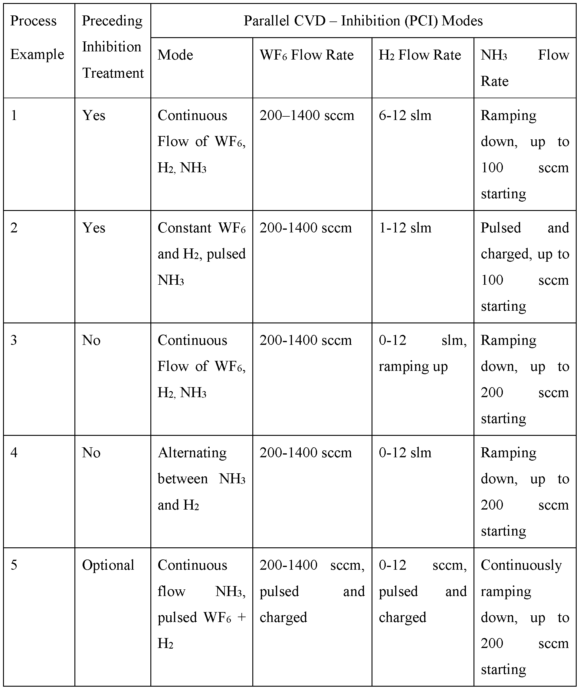

Claims
Priority Applications (2)
| Application Number | Priority Date | Filing Date | Title |
|---|---|---|---|
| CN202380085491.1A CN120380194A (en) | 2022-12-14 | 2023-12-12 | Fill with suppressed features |
| KR1020257023373A KR20250121107A (en) | 2022-12-14 | 2023-12-12 | Feature filling using suppression |
Applications Claiming Priority (2)
| Application Number | Priority Date | Filing Date | Title |
|---|---|---|---|
| US202263387493P | 2022-12-14 | 2022-12-14 | |
| US63/387,493 | 2022-12-14 |
Publications (1)
| Publication Number | Publication Date |
|---|---|
| WO2024129781A1 true WO2024129781A1 (en) | 2024-06-20 |
Family
ID=91485788
Family Applications (1)
| Application Number | Title | Priority Date | Filing Date |
|---|---|---|---|
| PCT/US2023/083696 Ceased WO2024129781A1 (en) | 2022-12-14 | 2023-12-12 | Feature fill using inhibition |
Country Status (4)
| Country | Link |
|---|---|
| KR (1) | KR20250121107A (en) |
| CN (1) | CN120380194A (en) |
| TW (1) | TW202444945A (en) |
| WO (1) | WO2024129781A1 (en) |
Citations (5)
| Publication number | Priority date | Publication date | Assignee | Title |
|---|---|---|---|---|
| CN101673660A (en) * | 2008-09-09 | 2010-03-17 | 中芯国际集成电路制造(北京)有限公司 | Processing method of gap filling and manufacturing method of shallow trench isolation groove |
| US20200185225A1 (en) * | 2015-05-18 | 2020-06-11 | Lam Research Corporation | Feature fill with multi-stage nucleation inhibition |
| US20200318236A1 (en) * | 2019-04-02 | 2020-10-08 | Gelest Technologies, Inc. | Process for Pulsed Thin Film Deposition |
| KR20210012786A (en) * | 2019-07-26 | 2021-02-03 | 에스케이하이닉스 주식회사 | Vertical semiconductor device and method for fabricating the same |
| US20220262640A1 (en) * | 2016-08-16 | 2022-08-18 | Lam Research Corporation | Method for preventing line bending during metal fill process |
-
2023
- 2023-12-12 WO PCT/US2023/083696 patent/WO2024129781A1/en not_active Ceased
- 2023-12-12 KR KR1020257023373A patent/KR20250121107A/en active Pending
- 2023-12-12 CN CN202380085491.1A patent/CN120380194A/en active Pending
- 2023-12-13 TW TW112148389A patent/TW202444945A/en unknown
Patent Citations (5)
| Publication number | Priority date | Publication date | Assignee | Title |
|---|---|---|---|---|
| CN101673660A (en) * | 2008-09-09 | 2010-03-17 | 中芯国际集成电路制造(北京)有限公司 | Processing method of gap filling and manufacturing method of shallow trench isolation groove |
| US20200185225A1 (en) * | 2015-05-18 | 2020-06-11 | Lam Research Corporation | Feature fill with multi-stage nucleation inhibition |
| US20220262640A1 (en) * | 2016-08-16 | 2022-08-18 | Lam Research Corporation | Method for preventing line bending during metal fill process |
| US20200318236A1 (en) * | 2019-04-02 | 2020-10-08 | Gelest Technologies, Inc. | Process for Pulsed Thin Film Deposition |
| KR20210012786A (en) * | 2019-07-26 | 2021-02-03 | 에스케이하이닉스 주식회사 | Vertical semiconductor device and method for fabricating the same |
Also Published As
| Publication number | Publication date |
|---|---|
| KR20250121107A (en) | 2025-08-11 |
| CN120380194A (en) | 2025-07-25 |
| TW202444945A (en) | 2024-11-16 |
Similar Documents
| Publication | Publication Date | Title |
|---|---|---|
| US20240234208A1 (en) | Void free low stress fill | |
| US11549175B2 (en) | Method of depositing tungsten and other metals in 3D NAND structures | |
| US10546751B2 (en) | Forming low resistivity fluorine free tungsten film without nucleation | |
| US20230122846A1 (en) | Feature fill with nucleation inhibition | |
| US20250183041A1 (en) | Low resistance molybdenum deposition for logic source/drain contacts | |
| US20250038050A1 (en) | Feature fill with nucleation inhibition | |
| WO2020210260A1 (en) | High step coverage tungsten deposition | |
| US20260026324A1 (en) | Tungsten wordline fill in high aspect ratio 3d nand architecture | |
| US20240376598A1 (en) | Process gas ramp during semiconductor processing | |
| WO2024129781A1 (en) | Feature fill using inhibition | |
| WO2024196896A1 (en) | Pulse ald sequence for low fluorine nucleation layer deposition | |
| US20250259894A1 (en) | Molybdenum integration and void-free fill | |
| US20250051908A1 (en) | Large grain tungsten growth in features | |
| WO2024102866A1 (en) | Pulse ald sequence for low fluorine wn deposition | |
| WO2025264711A1 (en) | Molybdenum deposition | |
| WO2025184150A1 (en) | Large grain molybdenum growth in features | |
| WO2026030353A1 (en) | Integrated molybdenum liner and tungsten fill | |
| WO2026024831A1 (en) | Microfabrication of low-resistance molybdenum interconnects | |
| WO2024129394A1 (en) | Ald tungsten fill with boosted thermal inhibition | |
| CN118786517A (en) | Low resistance Mo deposition for logic source/drain contacts |
Legal Events
| Date | Code | Title | Description |
|---|---|---|---|
| 121 | Ep: the epo has been informed by wipo that ep was designated in this application |
Ref document number: 23904471 Country of ref document: EP Kind code of ref document: A1 |
|
| WWE | Wipo information: entry into national phase |
Ref document number: 202380085491.1 Country of ref document: CN |
|
| ENP | Entry into the national phase |
Ref document number: 1020257023373 Country of ref document: KR Free format text: ST27 STATUS EVENT CODE: A-0-1-A10-A15-NAP-PA0105 (AS PROVIDED BY THE NATIONAL OFFICE) |
|
| WWE | Wipo information: entry into national phase |
Ref document number: 1020257023373 Country of ref document: KR |
|
| NENP | Non-entry into the national phase |
Ref country code: DE |
|
| WWP | Wipo information: published in national office |
Ref document number: 202380085491.1 Country of ref document: CN |
|
| WWP | Wipo information: published in national office |
Ref document number: 1020257023373 Country of ref document: KR |
|
| 122 | Ep: pct application non-entry in european phase |
Ref document number: 23904471 Country of ref document: EP Kind code of ref document: A1 |