WO2023060505A1 - 一种表面等离子体近场光刻掩模拓扑优化的方法及系统 - Google Patents
一种表面等离子体近场光刻掩模拓扑优化的方法及系统 Download PDFInfo
- Publication number
- WO2023060505A1 WO2023060505A1 PCT/CN2021/123793 CN2021123793W WO2023060505A1 WO 2023060505 A1 WO2023060505 A1 WO 2023060505A1 CN 2021123793 W CN2021123793 W CN 2021123793W WO 2023060505 A1 WO2023060505 A1 WO 2023060505A1
- Authority
- WO
- WIPO (PCT)
- Prior art keywords
- data
- mask
- field
- mask data
- imaging
- Prior art date
Links
Images


Classifications
-
- G—PHYSICS
- G03—PHOTOGRAPHY; CINEMATOGRAPHY; ANALOGOUS TECHNIQUES USING WAVES OTHER THAN OPTICAL WAVES; ELECTROGRAPHY; HOLOGRAPHY
- G03F—PHOTOMECHANICAL PRODUCTION OF TEXTURED OR PATTERNED SURFACES, e.g. FOR PRINTING, FOR PROCESSING OF SEMICONDUCTOR DEVICES; MATERIALS THEREFOR; ORIGINALS THEREFOR; APPARATUS SPECIALLY ADAPTED THEREFOR
- G03F7/00—Photomechanical, e.g. photolithographic, production of textured or patterned surfaces, e.g. printing surfaces; Materials therefor, e.g. comprising photoresists; Apparatus specially adapted therefor
- G03F7/70—Microphotolithographic exposure; Apparatus therefor
- G03F7/70483—Information management; Active and passive control; Testing; Wafer monitoring, e.g. pattern monitoring
- G03F7/70491—Information management, e.g. software; Active and passive control, e.g. details of controlling exposure processes or exposure tool monitoring processes
- G03F7/705—Modelling or simulating from physical phenomena up to complete wafer processes or whole workflow in wafer productions
-
- G—PHYSICS
- G03—PHOTOGRAPHY; CINEMATOGRAPHY; ANALOGOUS TECHNIQUES USING WAVES OTHER THAN OPTICAL WAVES; ELECTROGRAPHY; HOLOGRAPHY
- G03F—PHOTOMECHANICAL PRODUCTION OF TEXTURED OR PATTERNED SURFACES, e.g. FOR PRINTING, FOR PROCESSING OF SEMICONDUCTOR DEVICES; MATERIALS THEREFOR; ORIGINALS THEREFOR; APPARATUS SPECIALLY ADAPTED THEREFOR
- G03F1/00—Originals for photomechanical production of textured or patterned surfaces, e.g., masks, photo-masks, reticles; Mask blanks or pellicles therefor; Containers specially adapted therefor; Preparation thereof
- G03F1/36—Masks having proximity correction features; Preparation thereof, e.g. optical proximity correction [OPC] design processes
-
- G—PHYSICS
- G03—PHOTOGRAPHY; CINEMATOGRAPHY; ANALOGOUS TECHNIQUES USING WAVES OTHER THAN OPTICAL WAVES; ELECTROGRAPHY; HOLOGRAPHY
- G03F—PHOTOMECHANICAL PRODUCTION OF TEXTURED OR PATTERNED SURFACES, e.g. FOR PRINTING, FOR PROCESSING OF SEMICONDUCTOR DEVICES; MATERIALS THEREFOR; ORIGINALS THEREFOR; APPARATUS SPECIALLY ADAPTED THEREFOR
- G03F1/00—Originals for photomechanical production of textured or patterned surfaces, e.g., masks, photo-masks, reticles; Mask blanks or pellicles therefor; Containers specially adapted therefor; Preparation thereof
- G03F1/50—Mask blanks not covered by G03F1/20 - G03F1/34; Preparation thereof
-
- G—PHYSICS
- G03—PHOTOGRAPHY; CINEMATOGRAPHY; ANALOGOUS TECHNIQUES USING WAVES OTHER THAN OPTICAL WAVES; ELECTROGRAPHY; HOLOGRAPHY
- G03F—PHOTOMECHANICAL PRODUCTION OF TEXTURED OR PATTERNED SURFACES, e.g. FOR PRINTING, FOR PROCESSING OF SEMICONDUCTOR DEVICES; MATERIALS THEREFOR; ORIGINALS THEREFOR; APPARATUS SPECIALLY ADAPTED THEREFOR
- G03F7/00—Photomechanical, e.g. photolithographic, production of textured or patterned surfaces, e.g. printing surfaces; Materials therefor, e.g. comprising photoresists; Apparatus specially adapted therefor
- G03F7/70—Microphotolithographic exposure; Apparatus therefor
- G03F7/70425—Imaging strategies, e.g. for increasing throughput or resolution, printing product fields larger than the image field or compensating lithography- or non-lithography errors, e.g. proximity correction, mix-and-match, stitching or double patterning
- G03F7/70433—Layout for increasing efficiency or for compensating imaging errors, e.g. layout of exposure fields for reducing focus errors; Use of mask features for increasing efficiency or for compensating imaging errors
-
- G—PHYSICS
- G06—COMPUTING; CALCULATING OR COUNTING
- G06F—ELECTRIC DIGITAL DATA PROCESSING
- G06F30/00—Computer-aided design [CAD]
- G06F30/30—Circuit design
- G06F30/39—Circuit design at the physical level
- G06F30/392—Floor-planning or layout, e.g. partitioning or placement
-
- G—PHYSICS
- G06—COMPUTING; CALCULATING OR COUNTING
- G06F—ELECTRIC DIGITAL DATA PROCESSING
- G06F30/00—Computer-aided design [CAD]
- G06F30/30—Circuit design
- G06F30/39—Circuit design at the physical level
- G06F30/398—Design verification or optimisation, e.g. using design rule check [DRC], layout versus schematics [LVS] or finite element methods [FEM]
Definitions
- the present disclosure relates to the technical field of integrated circuits, in particular to a method and system for surface plasmon lithography (Surface Plasmon Lithography, SPL) mask topology optimization.
- SPL Surface Plasmon Lithography
- the current mainstream lithography system is the 193nm Deep Ultraviolet Lithography (DUV) lithography system, and the surface plasmon near-field imaging lithography has the advantages of high throughput, high resolution, high aspect ratio, high fidelity, and one-step Exposure and other advantages are potential technical solutions to replace the complex and expensive modern projection lithography technology.
- DUV Deep Ultraviolet Lithography
- Pixel-based inverse lithography can effectively increase the degree of freedom in optimization, but at the same time, the huge variable throughput poses a major challenge to computational complexity and increases the runtime of pattern optimization.
- the present disclosure provides a method and system for surface plasmon near-field lithography mask topology optimization, which are used to at least partially solve technical problems such as how to perform optical proximity effect compensation in surface plasmon near-field lithography.
- One aspect of the present disclosure provides a method for surface plasmon near-field lithography mask topology optimization, including: acquiring the first mask data and performing blurring and projection processing on it to obtain the second mask data; according to the second Perform forward calculation on the mask data and the preset surface plasmon near-field lithography conditions to obtain imaging data and forward field data; calculate the imaging error between the imaging data and the expected imaging data; perform a calculation on the second mask data Accompanying calculation to obtain accompanying field data; calculating the gradient matrix of the imaging error relative to the first mask data according to the forward field data and accompanying field data; updating the first mask data according to the gradient matrix, and repeating the above steps for iterative calculation, Until the optimized mask data is obtained and the final mask pattern is output.
- calculating the imaging error between the imaging data and the expected imaging data includes: judging whether the imaging error is smaller than a threshold or whether the current accumulated iteration number is greater than a set value: if so, output the current mask data as optimized mask data; otherwise , to continue the iterative calculation.
- the forward calculation includes: using the exposure light source to simulate; using the time domain finite difference algorithm to obtain the imaging data and the forward field data.
- performing adjoint calculations includes: using an adjoint excitation source for simulation; using a time-domain finite difference algorithm to solve and obtain adjoint field data.
- obtaining the first mask data includes: obtaining an initial mask pattern based on the expected imaging pattern; performing pixelation processing on the initial mask pattern to obtain the initial mask data and the expected imaging data; The mask data is used as the first mask data for blurring and projection processing.
- obfuscation includes:
- projection processing includes:
- ⁇ is the binarization parameter
- ⁇ is the binarization threshold
- the blurred mask data is the projection-processed mask data, that is, the second mask data.
- calculating the imaging error between the imaging data and the expected imaging data includes:
- the imaging error F is calculated using the following formula:
- P a (x, y) is the imaging data corresponding to the current mask data under the preset surface plasmon near-field lithography conditions
- P d (x, y) is the expected imaging data
- (x, y) is the coordinate in the imaging data
- m and n are the number of sampling points in the x and y directions corresponding to the imaging data.
- calculating the gradient matrix of the imaging error relative to the first mask data according to the forward field data and the accompanying field data includes:
- the gradient matrix is calculated using the following formula:
- G(r) is the gradient matrix
- n(r) is the refractive index distribution of the current mask data
- E for (r) is the forward field data
- E adj (r) is the accompanying field data.
- updating the first mask data according to the gradient matrix includes:
- the updated mask data is calculated using the following formula:
- s is the preset optimization step size
- ⁇ k (r) is the current mask data
- ⁇ k+1 (r) is the updated mask data
- G(r) is the gradient matrix
- k is the current iteration Algebra; wherein, all pixel values of the updated mask data are limited to the range of [0, 1], wherein pixel values greater than 1 are set to 1, and pixel values less than 0 are set to 0, between [0 , 1] the pixel values in the range remain unchanged.
- outputting the final mask pattern includes: outputting the current mask data as optimized mask data, extracting the edge of the optimized mask data using an edge smoothing method and removing pixelated jaggies, and then outputting the final mask pattern, wherein,
- the output optimized mask data is the current second mask data.
- Another aspect of the present disclosure provides a surface plasmon near-field lithography method, including: acquiring first mask data, performing blurring and projection processing on the first mask data, and obtaining second mask data; Perform forward calculation on the second mask data and the preset surface plasmon near-field lithography conditions to obtain imaging data and forward field data; calculate the imaging error between the imaging data and the expected imaging data; calculate the second mask Perform adjoint calculation on the data to obtain the adjoint field data; calculate the gradient matrix of the imaging error relative to the first mask data according to the forward field data and the adjoint field data; update the first mask data according to the gradient matrix, and repeat the above steps for iteration Calculate until the optimized mask data is obtained and the final mask pattern is output; perform surface plasmon near-field lithography according to the final mask pattern.
- a system for surface plasmon near-field lithography mask topology optimization including: a mask processing module, which is used to obtain the first mask data and perform blurring and projection processing on it to obtain The second mask data; the acquisition module is used to perform forward calculation according to the second mask data and the preset surface plasmon near-field lithography conditions to obtain imaging data and forward field data; the imaging error calculation module uses For calculating the imaging error between the imaging data and the expected imaging data; the accompanying field data calculation module is used to perform accompanying calculation on the second mask data to obtain the accompanying field data; the gradient matrix calculation module is used for according to the forward field data and Calculate the gradient matrix of the imaging error relative to the first mask data with the field data; the iterative calculation module is used to update the first mask data according to the gradient matrix, and repeat the above steps for iterative calculation until the optimized mask data is obtained and Output the final mask pattern.
- a mask processing module which is used to obtain the first mask data and perform blurring and projection processing on it to obtain The second mask data
- Another aspect of the present disclosure provides an electronic device, including: a memory, a processor, and a computer program stored on the memory and operable on the processor.
- the processor executes the computer program
- the processor executes the aforementioned surface A method for mask topology optimization in plasmonic near-field lithography.
- Another aspect of the present disclosure provides a computer-readable storage medium, on which a computer program is stored.
- the computer program is executed by a processor, the aforementioned method for surface plasmon near-field lithography mask topology optimization is implemented.
- Another aspect of the present disclosure provides a computer program product, including a computer program.
- the computer program When the computer program is executed by a processor, the aforementioned method for surface plasmon near-field lithography mask topology optimization is implemented.
- the disclosure provides a method and system for surface plasmon near-field lithography mask topology optimization, which introduces adjoint calculations on the basis of forward calculations, obtains optimized gradients, and adjusts and compensates the mask topology to improve imaging protection.
- the accuracy and product yield can not only be used to solve the existing near-field lithography pattern distortion problem, but also can compensate the strong coupling phenomenon in sub-wavelength electromagnetic structures such as optical proximity effect, stray light effect and mask shadow effect.
- the disclosure fuzzily filters out microstructures that cannot be processed smaller than the set threshold, ensures that the minimum size of any part of the mask pattern is greater than or equal to the set threshold, and ensures that the mask feature size satisfies manufacturability constraints; mask manufacturability was further improved by correcting for unmanufacturable edge aliasing in pixelated mask patterns.
- FIG. 1 schematically shows a schematic diagram of an application scenario of a method for topology optimization of a surface plasmon near-field lithography mask according to an embodiment of the present disclosure
- FIG. 2 schematically shows a flowchart of a method for topology optimization of a surface plasmon near-field lithography mask according to an embodiment of the present disclosure
- FIG. 3 schematically shows a flowchart of a method for acquiring first mask data in a method for surface plasmon near-field lithography mask topology optimization according to an embodiment of the present disclosure
- FIG. 4 schematically shows a flowchart of a method for performing accompanying calculations in a method for topological optimization of a surface plasmon near-field lithography mask according to an embodiment of the present disclosure
- Fig. 5 schematically shows a flow chart of a method for topology optimization of a surface plasmon near-field lithography mask according to an exemplary embodiment of the present disclosure
- Fig. 6 schematically shows a schematic diagram corresponding to initial mask data, mask data after blur processing, and mask data after projection processing according to Embodiment 1 of the present disclosure
- FIG. 7 schematically shows a schematic diagram corresponding to the initial mask data and the corresponding imaging data in the photoresist according to Embodiment 1 of the present disclosure
- FIG. 8 schematically shows an iterative evolution diagram of the graph corresponding to the second mask data in the mask topology optimization process according to Embodiment 1 of the present disclosure
- FIG. 9 schematically shows the mask data obtained according to the first embodiment of the present disclosure and the corresponding graphic diagram corresponding to the imaging data in the photoresist;
- FIG. 10 schematically shows the mask data before and after optimization based on this method and the corresponding graphics corresponding to the imaging data in the photoresist using the structure 101 according to Embodiment 2 of the present disclosure
- FIG. 11 schematically shows the mask data before and after optimization based on this method using the structure 102 in Embodiment 3 of the present disclosure and the corresponding graphics corresponding to the imaging data in the corresponding photoresist;
- FIG. 12 schematically shows a block diagram of a system for topology optimization of a surface plasmon near-field lithography mask according to an embodiment of the present disclosure
- Fig. 13 schematically shows a block diagram of an electronic device suitable for implementing the method described above according to an embodiment of the present disclosure.
- the topology optimization technology for surface plasmon near-field lithography mask based on adjoint algorithm is an important lithography resolution enhancement technology, which modulates the light incident on the photoresist by optimizing the mask topology field intensity distribution, thereby improving the resolution and image fidelity of lithography systems.
- the mask is represented by pixelated graphics, which has a high degree of freedom in optimization.
- only two simulation calculations are required to evaluate the gradient of the mask topology along the direction of lithographic imaging quality optimization. Update information, greatly reducing computing throughput and improving optimization speed.
- FIG. 1 schematically shows a schematic diagram of an application scenario of a method for topology optimization of a surface plasmon near-field lithography mask according to an embodiment of the present disclosure. It should be noted that what is shown in FIG. 1 is only an example of an application scenario to which the embodiment of the present disclosure can be applied, so as to help those skilled in the art understand the technical content of the present disclosure, but it does not mean that the embodiment of the present disclosure cannot be used in other device, system, environment or scenario.
- the surface plasmon near-field lithography structure of the embodiment of the present disclosure can be shown as 101, including a mask (SiO 2 +Cr), an air spacer layer (Air), a metal layer (Ag), a photolithography Structure of glue (Pr), metal reflective layer (Ag) and substrate (SiO 2 ).
- the interface diagram of the surface plasmon near-field lithography structure is shown in 102 and 103.
- the lithography structure may also include a mask (SiO 2 +Cr), an air spacer layer (Air), a photoresist (Pr), and a metal reflective layer (Ag) and substrate (SiO 2 ) structure (as shown in 102), may also include mask (SiO 2 +Cr), air spacer layer (Air), metal layer (Ag), photoresist (Pr) and the structure of the substrate (SiO 2 ) (as shown in 103 ), as long as the structure can realize the surface plasmon near-field lithography.
- patterns on masks are transferred to semiconductor chips, exhibiting poor contrast, poor fidelity, and non-uniformity.
- the present disclosure provides a mask topology optimization method for surface plasmon near-field lithography based on an adjoint algorithm, which can provide better mask patterns according to actual needs, and compensate the surface plasmon near-field lithography system.
- Subwavelength electromagnetic effects such as optical proximity effect, stray light effect, mask shadow effect, etc.
- Fig. 2 schematically shows a flowchart of a method for topology optimization of a surface plasmon near-field lithography mask according to an embodiment of the present disclosure.
- the method for topology optimization of the surface plasmon near-field lithography mask includes:
- the first mask data is acquired and blurred and projected are processed to obtain second mask data.
- the second mask data can be obtained by using the initial mask data or the updated mask data as the first mask data to perform blurring and projection processing.
- forward calculation is performed according to the second mask data and preset surface plasmon near-field lithography conditions to obtain imaging data and forward field data.
- This step evaluates the surface plasmon near-field imaging performance of the mask based on the set surface plasmon near-field lithography structure.
- This step calculates the imaging performance of the mask pattern in the photoresist under the excitation source of the exposure light source, and at the same time obtains the forward field data for the subsequent gradient update of the accompanying algorithm.
- This process is referred to as forward calculation or forward calculation in this disclosure. towards simulation.
- the forward field data here refers to the vector electric field data in the mask.
- This operation aims to calculate the error between each pixel of the imaging pattern in the corresponding photoresist of the current imaging mask and the target pattern, and it is specifically realized through data calculation.
- the error set in this disclosure is aimed at the graphic area error, and its value needs to be selected according to specific issues such as the complexity of the optimized mask, the size of the pixelated grid, the size of the overall mask, and the expected tolerable degree of graphic distortion , for general integrated circuit masks, it is often necessary to control the error of the optimized imaging area within 1% to 3%.
- the adjoint calculation is performed on the second mask data.
- the adjoint calculation on the basis of forward calculation, the calculation of replacing the imaging monitor in the photoresist with a specific accompanying source is called adjoint calculation.
- the gradient matrix is obtained by using the results of forward calculation and adjoint calculation and the optimization algorithm for updating the mask called the adjoint algorithm.
- the adjoint field is the vector electric field data in the mask calculated based on a given adjoint excitation source simulation.
- a gradient matrix of the imaging error with respect to the first mask data is calculated based on the forward field data and the accompanying field data.
- step S3 According to the result of the forward calculation in step S1 and the result of the accompanying calculation in step S3, the positive and negative contribution of each pixel to the imaging quality is calculated, that is, the gradient matrix is obtained.
- the first mask data is updated according to the gradient matrix, and the above steps are repeated for iterative calculation until optimized mask data is obtained and a final mask pattern is output.
- the pixelated mask data is updated according to the gradient matrix obtained in step S4, and steps S0 to S5 are performed in a loop until the imaging performance in step S2 meets the design index.
- the disclosed method adds adjoint simulation, gradient calculation, and mask processing, and quickly iteratively converges based on prior physical information. Better mask patterns.
- calculating the imaging error between the imaging data and the expected imaging data includes: judging whether the imaging error is smaller than a threshold or whether the current cumulative iteration number is greater than a set value: if so, outputting the current mask data as an optimized Mask data; otherwise, proceed with iterative computation.
- the current mask data used in the description in this disclosure represents the mask data processed in the corresponding steps in the current iterative cycle, which can be the first mask data or the second mask data, and those skilled in the art can The processing steps to understand the meaning of the current mask data.
- the output current mask data is the second mask data that satisfies the judgment criteria in the current iterative cycle, so as to facilitate actual mask processing.
- the imaging performance of the mask pattern is within a preset threshold, or whether the number of iterations exceeds the maximum number of iterations.
- the imaging performance is represented by an imaging error function in this disclosure.
- the current mask data is output as the optimized mask data; otherwise, enter step S0 for iterative calculation.
- the number of optimization iterations required by the present disclosure usually requires 100-300 generations to reach the optimal value of convergence.
- Fig. 3 schematically shows a flowchart of a method for acquiring first mask data in the method for surface plasmon near-field lithography mask topology optimization according to an embodiment of the present disclosure.
- the method for obtaining the first mask includes:
- an initial mask pattern is acquired based on an expected imaging pattern.
- the expected imaging pattern is the target pattern.
- the initial mask pattern is pixelated to obtain initial mask data and expected imaging data.
- the initial mask data is used as the first mask data of the first iteration, and the expected imaging data corresponds to the initial mask data.
- an initial mask pattern is determined based on the target pattern, and the initial mask pattern is pixelated to obtain initial mask data.
- the data defining the graphics in this step is a binary and pixelated matrix.
- the expected imaging data is P d (x, y), and the initial mask data is used as the first mask data ⁇ 1 (r) of the first generation iteration.
- the initial mask pattern is rasterized It is divided into m ⁇ n pixelated grids with equal intervals, and the center coordinates of each pixel block take discrete values at this time.
- the initial mask data or the updated mask data is used as the first mask data to perform blur processing and projection processing to obtain second mask data.
- fuzzy processing is performed on the initial mask data or the updated mask data to remove structures smaller than the minimum design rules that cannot be processed; then binary projection processing is performed on the mask data after fuzzy processing to obtain Subsequent calculations are performed on the mask data after projection of the physical model.
- This step can meet the actual mask processing requirements.
- linear blurring is performed on the initial mask data ⁇ (r) or the updated mask data to obtain and binarized projection processing to get
- the linear blur function is:
- the binarized projection function is:
- ⁇ is the binarization parameter
- ⁇ is the binarization threshold
- the blurred mask data is the projection-processed mask data, that is, the second mask data.
- the value of the mask matrix of the second mask data after binarization will be close to 0 or 1, which satisfies the physical meaning that the actual mask has only two states of transparent or opaque.
- the SPL imaging performance of the mask pattern is evaluated based on a given surface plasmon lithography structure, and the imaging data of the current mask data in the photoresist is obtained.
- the disclosure is applicable to the optimization of any mask pattern, and for a complex mask pattern with multiple directions, TM/TE polarized plane waves of two independent exposures are used as the excitation source of the exposure light source for forward calculation. Therefore, for independent exposure of TM/TE dual-polarized plane wave light sources, the electric field in the photoresist can be strictly calculated by the finite-difference time-domain algorithm, and the complex coupling between subwavelength structures and the effects of stray light on the spatial image will be considered in the full-wave calculation. Impact.
- the imaging result in the photoresist corresponding to the current mask data is the sum of the three component intensities of the electric field.
- P a ⁇
- E for (r) Simultaneously monitor the vector field in the mask, called the forward field E for (r).
- 702 is the pattern corresponding to the light intensity distribution data in the photoresist after the light passes through the initial mask pattern and the SPL system in the first embodiment
- 703 is the exposure pattern corresponding to the binarized imaging data.
- the currently calculated imaging error function value satisfies the set threshold, or the number of iterations is greater than the maximum number of iterations, then output the current mask data as the optimized mask data, otherwise continue the iterative calculation.
- FIG. 4 schematically shows a flowchart of a method for performing accompanying calculations in a method for topological optimization of a surface plasmon near-field lithography mask according to an embodiment of the present disclosure.
- the method for performing accompanying calculation on the second mask data includes:
- the adjoint field data is obtained by using the time domain finite difference algorithm to solve.
- the function P a (x, y) does not satisfy the Cauchy-Riemann condition, it is not conducive to gradient optimization, so here the P′ a (x, y) approximated by the Sig( ⁇ ) shape function of the actual imaging graph represents the current imaging graphics, ie
- the adjoint calculation can be strictly solved by using the time-domain finite difference algorithm, and the adjoint field E adj (r) can be obtained by monitoring the vector field components in the mask.
- the imaging error function F is calculated relative to the first mask data ⁇ ( The gradient matrix of r) Where n(r) is the refractive index distribution of the current mask data, and the obtained gradient matrix represents the positive and negative contribution of each pixel of the current mask data to the imaging quality.
- step S1 After the update, limit all pixel values of the updated mask data within the range [0, 1] to ensure that the mask data conforms to the actual physical meaning, where the pixel values greater than 1 are set to 1, and the pixel values less than 0 Set to 0, the pixel values in the range [0, 1] remain unchanged, then return to step S1.
- outputting the current mask data as optimized mask data and outputting the final mask pattern includes: outputting the current mask data as optimized mask data, and extracting the optimized mask by edge smoothing method After the edges of the data are removed and pixelated aliasing is removed, the final mask pattern is output.
- the output optimized mask data is the current second mask data, so as to meet actual processing requirements.
- the pixelization density parameter of the mask is used as an optimization parameter, and the shape of the optimized mask pattern is finally determined through topology optimization.
- the mask processing part in this disclosure is to divide the mask pattern into pixelated grids and obtain pixelated mask data, each pixel can be represented by a value between 0-1, where 0 represents a transparent mask , 1 means an opaque mask.
- adjoint calculation is introduced to obtain optimized gradient and adjust and compensate mask topology to improve imaging fidelity and product yield.
- the optimized gradient direction of each generation is obtained, and then quickly converges to the optimal mask structure parameters.
- the compensation of the subwavelength electromagnetic proximity effect is realized, and a higher imaging fidelity is obtained.
- the optimized mask obtained above can also be used in the surface plasmon near-field lithography method.
- the disclosed method includes the following steps:
- Step 501 Determine the expected imaging pattern, that is, the target pattern, determine an initial mask pattern based on the target pattern, perform pixelation processing on the initial mask pattern, and obtain and input initial mask data.
- the mask data defined in this step is a binary, pixelated matrix.
- the initial mask data is defined as the first mask data of the first iteration, and the updated mask data obtained by subsequent iterations is jointly determined by the first mask data of the previous generation and the gradient matrix.
- Step 502 Perform blurring and projection processing on the first mask data, ie initial mask data or updated mask data, to obtain second mask data.
- the initial mask data or the updated mask data are blurred to remove structures smaller than the minimum design rule that cannot be processed; then, binary projection processing is performed on the blurred mask data to obtain the post-projection processing The mask data to make it meet the actual physical model.
- Step 503 Evaluate the surface plasmon near-field imaging performance of the current mask data based on the set surface plasmon near-field lithography structure. This step calculates the imaging performance of the current mask data in the photoresist under the excitation of the exposure light source, and at the same time obtains the forward field data for the gradient update of the subsequent adjoint algorithm.
- the vector electric field distribution value in the mask is the forward field , this process is referred to as forward calculation or forward simulation in this disclosure, which is equivalent to the aforementioned S1.
- Step 504 Determine whether the imaging performance of the current mask data is within a preset threshold, or whether the number of iterations exceeds the maximum number of iterations.
- the imaging performance is represented by an imaging error function in the present disclosure, which is defined as the square of the difference between the imaging pattern of the current mask data in the corresponding photoresist and the expected imaging data for each pixel.
- an imaging error function in the present disclosure, which is defined as the square of the difference between the imaging pattern of the current mask data in the corresponding photoresist and the expected imaging data for each pixel.
- Step 505 Perform adjoint calculation on the second mask data based on the adjoint algorithm proposed in the present disclosure.
- the accompanying calculation on the basis of the forward calculation, the calculation of replacing the imaging monitor in the photoresist with a specific accompanying source is called the accompanying calculation, and the accompanying calculation is used to simulate and calculate the virtual accompanying field data according to the given accompanying excitation source , using the results of forward calculation and adjoint calculation to obtain the gradient update mask optimization algorithm is called adjoint algorithm, which is equivalent to the aforementioned S3.
- steps 503 and 505 the forward calculation and the adjoint calculation can be quickly and accurately calculated using the finite difference time domain method.
- Step 506 According to the result of the forward calculation in step 503 and the result of the accompanying calculation in step 505, calculate the sign and magnitude of each pixel's contribution to the imaging quality, that is, obtain the gradient matrix, which is equivalent to the aforementioned S4.
- Step 507 Update the pixelated first mask data according to the gradient matrix obtained in step 506 to obtain an updated mask matrix, and perform steps 502 to 507 in a loop until the imaging performance in step 504 meets the design index, which is equivalent to the aforementioned S5 .
- Step 508 Output the current mask data as optimized mask data after the optimization, use the edge smoothing method to extract edges and remove useless and unmanufacturable pixelated edge aliases, and obtain the final mask pattern after topology optimization.
- Fig. 1 is the structure that comprises mask, air spacer layer, metal layer, photoresist, metal reflective layer and substrate, and mask thickness is set to be 50nm in the present embodiment, air spacer is 20nm, photoresist upper layer metal layer is 20nm , the lower metal layer is 70nm, and the thickness of the photoresist is 40nm.
- Figure 6 shows in sequence 601 the initial mask data ⁇ 1 (r), 602 the mask data after blurring processing 603 Mask data after binary projection processing The corresponding graphic diagram
- 701 is the graph corresponding to the initial mask data, which corresponds to the expected imaging graph, that is, the target graph, wherein the white area represents the transparent part, and the black represents the non-transparent mask part, and its key feature size is 70nm;
- 702 represents the pattern corresponding to the light intensity distribution data in the photoresist through the SPL system using 701 as the mask pattern, and
- the calculated imaging error is 9.1911%.
- the imaging error threshold is set to 1.5%, and the number of optimization iterations is set to 250 generations. It can be seen that the set threshold is not met.
- the gradient matrix is obtained based on the accompanying field data and the forward field data, and the pixel values of the first mask data are updated, and iterations are repeated.
- the optimized mask data is finally obtained and output to obtain the final mask pattern.
- FIG. 9 is a schematic diagram of the mask data optimized by the disclosed method and corresponding to the imaging data in the photoresist.
- 901 is the graph corresponding to the mask data obtained by topology optimization using the disclosed method
- 902 is the graph corresponding to the light intensity distribution data in the photoresist through the SPL system after using 901 as the mask graph
- 903 is the light intensity of 902
- FIG. 10 shows a schematic diagram of the mask data before and after optimization using the adjoint algorithm-based mask topology optimization method of the present disclosure and the corresponding graphics corresponding to the imaging data in the photoresist in the SPL lithography structure shown in 101 in FIG. 1 , Three cases before and after mask pattern optimization are listed. 1001, 1005, and 1009 are initial mask patterns; 1002, 1006, and 1010 are corresponding photoresist imaging patterns after binary exposure processing; 1003, 1007, and 1011 are final mask patterns output after iteration; 1004, 1008 and 1012 are the final imaging graphics.
- the thickness of the mask is 40nm
- the air gap is 30nm
- the upper metal layer of the photoresist is 20nm
- the lower metal layer is 50nm
- the thickness of the photoresist is 30nm
- the characteristic size of the mask is 60nm.
- the corresponding imaging error values of the three mask patterns are reduced from 12.3%, 3%, and 6.8% to 2.1%, 2.1%, and 2.7% respectively after being optimized in the present disclosure.
- the imaging error thresholds are all set to 2%, and the number of iterations is 200 generations.
- FIG. 11 shows a schematic diagram of the mask data before and after optimization using the adjoint algorithm-based mask topology optimization method of the present disclosure and the corresponding graphics corresponding to the imaging data in the photoresist in the SPL lithography structure shown in 102 in FIG. 1 , Three cases before and after mask pattern optimization are listed. 1101, 1105, 1109 are initial mask patterns; 1102, 1106, 1110 are corresponding photoresist imaging patterns after binary exposure processing; 1103, 1107, 1111 are final mask patterns output after iteration; 1104, 1108 and 1112 are final imaging graphics.
- the thickness of the mask is 40nm
- the air gap is 20nm
- the thickness of the photoresist is 30nm
- the lower metal layer is 70nm
- the characteristic size of the mask is 70nm.
- the corresponding imaging error values of the three mask patterns are reduced from 4.2%, 6.1%, and 4.7% to 0.7%, 0.6%, and 1.4% respectively after being optimized in the present disclosure.
- the imaging error thresholds are all set to 0.5%, and the number of iterations is 120 generations.
- Fig. 12 schematically shows a block diagram of a system for surface plasmon near-field lithography mask topology optimization according to an embodiment of the present disclosure.
- the system 1200 for topological optimization of surface plasmon near-field lithography masks includes: mask processing module 1210, acquisition module 1220, imaging error calculation module 1230, accompanying field data calculation module 1240, gradient matrix calculation module 1250. Iterative calculation module 1260.
- the mask processing module 1210 is configured to acquire the first mask data and perform blur processing and projection processing on it to obtain second mask data. According to an embodiment of the present disclosure, the mask processing module 1210 may, for example, be used to execute step S1 described above with reference to FIG. 2 , which will not be repeated here.
- the acquisition module 1220 is configured to perform forward calculation according to the mask data and preset surface plasmon near-field lithography conditions to obtain imaging data and forward field data; according to an embodiment of the present disclosure, the acquisition module 1220 can be used, for example After performing step S2 described above with reference to FIG. 2 , details are not repeated here.
- the imaging error calculation module 1230 is configured to calculate the imaging error between the imaging data and the expected imaging data; according to an embodiment of the present disclosure, the imaging error calculation module 1230 may be used to execute step S3 described above with reference to FIG. 2 , I won't repeat them here.
- the adjoint field data calculation module 1240 is configured to perform adjoint calculation on the mask data to obtain the adjoint field data; according to an embodiment of the present disclosure, the adjoint field data calculation module 1240 can, for example, be used to execute S4 described above with reference to FIG. 2 The steps are not repeated here.
- the gradient matrix calculation module 1250 is configured to calculate the gradient matrix of the imaging error relative to the first mask data according to the forward field data and the accompanying field data; according to an embodiment of the present disclosure, the gradient matrix calculation module 1250 can be used to perform the Step S5 described herein with reference to FIG. 2 will not be repeated here.
- the iterative calculation module 1260 is configured to update the first mask data according to the gradient matrix, and repeat the above steps to perform iterative calculation until the optimized mask data is obtained and the final mask pattern is output; according to an embodiment of the present disclosure, the iterative calculation The module 1260 can be used, for example, to execute step S6 described above with reference to FIG. 2 , which will not be repeated here.
- any multiple of the modules, sub-modules, units, and sub-units, or at least part of the functions of any multiple of them may be implemented in one module.
- Any one or more of modules, submodules, units, and subunits according to the embodiments of the present disclosure may be implemented by being divided into multiple modules.
- modules, submodules, units, and subunits may be at least partially implemented as hardware circuits, such as field programmable gate arrays (FPGAs), programmable logic arrays (PLAs), system-on-chip, system-on-substrate, system-on-package, application-specific integrated circuit (ASIC), or hardware or firmware that may be implemented by any other reasonable means of integrating or packaging circuits, or in a combination of software, hardware, and firmware Any one of these implementations or an appropriate combination of any of them.
- FPGAs field programmable gate arrays
- PLAs programmable logic arrays
- ASIC application-specific integrated circuit
- hardware or firmware hardware or firmware that may be implemented by any other reasonable means of integrating or packaging circuits, or in a combination of software, hardware, and firmware Any one of these implementations or an appropriate combination of any of them.
- one or more of the modules, submodules, units, and subunits according to the embodiments of the present disclosure may be at least partially implemented as computer program modules, and when the
- any number of the mask processing module 1210, the acquisition module 1220, the imaging error calculation module 1230, the accompanying field data calculation module 1240, the gradient matrix calculation module 1250, and the iterative calculation module 1260 can be combined and implemented in one module, or Any module of can be split into multiple modules. Alternatively, at least part of the functions of one or more of these modules may be combined with at least part of the functions of other modules and implemented in one module.
- At least one of the mask processing module 1210, the acquisition module 1220, the imaging error calculation module 1230, the accompanying field data calculation module 1240, the gradient matrix calculation module 1250, and the iterative calculation module 1260 can be at least partially implemented is a hardware circuit, such as a field programmable gate array (FPGA), a programmable logic array (PLA), a system on a chip, a system on a substrate, a system on a package, or an application-specific integrated circuit (ASIC), or it can be implemented by integrating the circuit or Any other reasonable way of encapsulation, such as hardware or firmware, or any one of the three implementation ways of software, hardware and firmware, or an appropriate combination of any of them.
- FPGA field programmable gate array
- PLA programmable logic array
- ASIC application-specific integrated circuit
- At least one of the mask processing module 1210, the acquisition module 1220, the imaging error calculation module 1230, the accompanying field data calculation module 1240, the gradient matrix calculation module 1250, and the iterative calculation module 1260 can be at least partially implemented as a computer program module, When the computer program modules are executed, corresponding functions can be performed.
- Fig. 13 schematically shows a block diagram of an electronic device suitable for implementing the method described above according to an embodiment of the present disclosure.
- the electronic device shown in FIG. 13 is only an example, and should not limit the functions and scope of use of the embodiments of the present disclosure.
- the electronic device 1300 described in this embodiment includes: a processor 1301, which can be loaded into a random access memory (RAM) according to a program stored in a read-only memory (ROM) 1302 or from a storage part 1308. ) 1303 to perform various appropriate actions and processing.
- the processor 1301 may include, for example, a general-purpose microprocessor (eg, a CPU), an instruction set processor and/or related chipsets and/or a special-purpose microprocessor (eg, an application-specific integrated circuit (ASIC)), and the like.
- Processor 1301 may also include on-board memory for caching purposes.
- the processor 1301 may include a single processing unit or multiple processing units for executing different actions of the method flow according to the embodiments of the present disclosure.
- the processor 1301, ROM 1302, and RAM 1303 are connected to each other through a bus 1304.
- the processor 1301 executes various operations according to the method flow of the embodiments of the present disclosure by executing programs in the ROM 1302 and/or RAM 1303. It should be noted that programs may also be stored in one or more memories other than ROM 1302 and RAM 1303.
- the processor 1301 can also perform various operations according to the method flow of the embodiments of the present disclosure by executing programs stored in one or more memories.
- the electronic device 1300 may further include an input/output (I/O) interface 1305 which is also connected to the bus 1304 .
- System 1300 may also include one or more of the following components connected to I/O interface 1305: an input section 1306 including a keyboard, mouse, etc.; etc.; a storage section 1308 including a hard disk or the like; and a communication section 1309 including a network interface card such as a LAN card, a modem, or the like.
- the communication section 1309 performs communication processing via a network such as the Internet.
- a drive 1310 is also connected to the I/O interface 1305 as needed.
- a removable medium 1311 such as a magnetic disk, an optical disk, a magneto-optical disk, a semiconductor memory, etc., is mounted on the drive 1310 as necessary so that a computer program read therefrom is installed into the storage section 1308 as necessary.
- the method flow according to the embodiments of the present disclosure can be implemented as a computer software program.
- the embodiments of the present disclosure include a computer program product, which includes a computer program carried on a computer-readable storage medium, where the computer program includes program codes for executing the methods shown in the flowcharts.
- the computer program may be downloaded and installed from a network via communication portion 1309 and/or installed from removable media 1311 .
- the processor 1301 When the computer program is executed by the processor 1301, the above-mentioned functions defined in the system of the embodiment of the present disclosure are executed.
- the above-described systems, devices, devices, modules, units, etc. may be implemented by computer program modules.
- Embodiments of the present disclosure also provide a computer-readable storage medium, which may be included in the device/apparatus/system described in the above-mentioned embodiments; or may exist independently without being assembled into the equipment/device/system.
- the computer-readable storage medium carries one or more programs, and when the one or more programs are executed, the method for topology optimization of a surface plasmon near-field lithography mask according to an embodiment of the present disclosure is realized.
- the computer-readable storage medium may be a non-volatile computer-readable storage medium, such as may include but not limited to: portable computer disk, hard disk, random access memory (RAM), read-only memory (ROM) , erasable programmable read-only memory (EPROM or flash memory), portable compact disk read-only memory (CD-ROM), optical storage device, magnetic storage device, or any suitable combination of the above.
- a computer-readable storage medium may be any tangible medium containing or storing a program that can be used by or in conjunction with an instruction execution system, apparatus, or device.
- the computer-readable storage medium may include the ROM 1302 and/or the RAM 1303 and/or one or more memories other than the ROM 1302 and the RAM 1303 described above.
- Embodiments of the present disclosure also include a computer program product, which includes a computer program including program codes for executing the methods shown in the flowcharts.
- the program code is used to make the computer system implement the method for surface plasmon near-field photolithography mask topology optimization provided by the embodiments of the present disclosure.
- the computer program may rely on tangible storage media such as optical storage devices and magnetic storage devices.
- the computer program can also be transmitted and distributed in the form of a signal on network media, downloaded and installed through the communication part 1309, and/or installed from the removable media 1311.
- the program code contained in the computer program can be transmitted by any appropriate network medium, including but not limited to: wireless, wired, etc., or any appropriate combination of the above.
- the computer program may be downloaded and installed from a network via communication portion 1309 and/or installed from removable media 1311 .
- the computer program is executed by the processor 1301, the above-mentioned functions defined in the system of the embodiment of the present disclosure are performed.
- the above-described systems, devices, devices, modules, units, etc. may be implemented by computer program modules.
- the program codes for executing the computer programs provided by the embodiments of the present disclosure can be written in any combination of one or more programming languages, specifically, high-level procedural and/or object-oriented programming language, and/or assembly/machine language to implement these computing programs.
- Programming languages include, but are not limited to, programming languages such as Java, C++, python, "C" or similar programming languages.
- the program code can execute entirely on the user computing device, partly on the user device, partly on the remote computing device, or entirely on the remote computing device or server.
- the remote computing device may be connected to the user computing device through any kind of network, including a local area network (LAN) or a wide area network (WAN), or may be connected to an external computing device (e.g., using an Internet service provider). business to connect via the Internet).
- LAN local area network
- WAN wide area network
- Internet service provider an Internet service provider
- each functional module in each embodiment of the present disclosure may be integrated into one processing module, each module may exist separately physically, or two or more modules may be integrated into one module.
- the above-mentioned integrated modules can be implemented in the form of hardware or in the form of software function modules. If the integrated modules are realized in the form of software function modules and sold or used as independent products, they can be stored in a computer-readable storage medium. Based on such an understanding, the essence of the technical solution of the present disclosure or the part that contributes to the prior art, or all or part of the technical solution can be embodied in the form of software products.
- each block in a flowchart or block diagram may represent a module, program segment, or portion of code that includes one or more logical functions for implementing specified executable instructions.
- the functions noted in the block may occur out of the order noted in the figures. For example, two blocks shown in succession may, in fact, be executed substantially concurrently, or they may sometimes be executed in the reverse order, depending upon the functionality involved.
- each block in the block diagrams or flowchart illustrations, and combinations of blocks in the block diagrams or flowchart illustrations can be implemented by a dedicated hardware-based system that performs the specified function or operation, or can be implemented by a A combination of dedicated hardware and computer instructions.
Landscapes
- Physics & Mathematics (AREA)
- General Physics & Mathematics (AREA)
- Engineering & Computer Science (AREA)
- Computer Hardware Design (AREA)
- Theoretical Computer Science (AREA)
- Evolutionary Computation (AREA)
- Geometry (AREA)
- General Engineering & Computer Science (AREA)
- Architecture (AREA)
- Exposure And Positioning Against Photoresist Photosensitive Materials (AREA)
- Preparing Plates And Mask In Photomechanical Process (AREA)
Abstract
本公开提供了一种表面等离子体近场光刻掩模拓扑优化的方法,包括:获取第一掩模数据并对其进行模糊处理与投影处理,得到第二掩模数据;根据第二掩模数据和预设的表面等离子体近场光刻的条件进行正向计算,得到成像数据以及正向场数据;计算成像数据与预期成像数据之间的成像误差;对第二掩模数据进行伴随计算,得到伴随场数据;根据正向场数据和伴随场数据计算成像误差相对于第一掩模数据的梯度矩阵;根据梯度矩阵对第一掩模数据进行更新,重复上述步骤进行迭代计算,直至获得优化的掩模数据并输出最终掩模图形。本公开还提供了一种表面等离子体近场光刻掩模拓扑优化的系统、电子设备、计算机可读存储介质和程序产品。本公开能够解决现有近场光刻图案畸变的问题,补偿亚波长电磁结构中的强耦合现象。
Description
本公开涉及集成电路技术领域,具体涉及一种表面等离子体近场光刻(Surface Plasmon Lithography,SPL)掩模拓扑优化的方法及系统。
在现代复杂微电子集成电路制造中,需要先设计集成电路的掩模版图案,而后再通过光刻技术将掩模版图案转移到半导体芯片上。目前主流的光刻系统是193nm的深紫外(Deep Ultraviolet Lithography,DUV)光刻系统,而表面等离子体近场成像光刻具有吞吐量大、分辨率高、纵横比高、保真度高、一步曝光等优点,是替代复杂昂贵的现代投影光刻技术的潜在技术方案。
同时,在集成电路制造过程中必须严格控制光刻中的图像保真度,以提高半导体器件的性能、效率和产量。然而,在对高密度集成的复杂掩模版图案进行曝光转移处理时,会表现出较差的对比度、较差的保真度和不均匀性。为了提高光刻系统的分辨率和成像保真度,逆向光刻技术(Inverse Lithography Technology,ILT),尤其是光学邻近效应矫正(Optical Proximity Correction,OPC)被广泛地用于通过变形掩模来补偿光学邻近效应、杂散光效应、掩模阴影效应等不利影响引起的图像失真。由于非线性成像模型和非线性光刻胶效应,传统的OPC方法难以应用于具有亚波长电磁结构的表面等离子体近场光刻中。
因此,本领域技术人员亟需一种高效、快速、低成本的光学邻近效应补偿方法,对目标图案进行调整补偿,以满足面积误差的要求,提高产品良率。基于像素的逆向光刻技术可以有效地提高优化自由度,但同时巨大的变量吞吐量对计算复杂度带来了重大挑战,并增加了图案优化的运行时间。
发明内容
(一)要解决的技术问题
针对上述问题,本公开提供了一种表面等离子体近场光刻掩模拓扑优化的方法及系统,用于至少部分解决表面等离子体近场光刻中如何进行光学邻近效应补偿等技术问题。
(二)技术方案
本公开一方面提供了一种表面等离子体近场光刻掩模拓扑优化的方法,包括:获取第一掩模数据并对其进行模糊处理与投影处理,得到第二掩模数据;根据第二掩模数据和预设的表面等离子体近场光刻的条件进行正向计算,得到成像数据以及正向场数据;计算成像数据与预期成像数据之间的成像误差;对第二掩模数据进行伴随计算,得到伴随场数据;根据正向场数据和伴随场数据计算成像误差相对于第一掩模数据的梯度矩阵;根据梯度矩阵对第一掩模数据进行更新,重复上述步骤进行迭代计算,直至获得优化的掩模数据并输出最终掩模图形。
进一步地,计算成像数据与预期成像数据之间的成像误差包括:判断成像误差是否小于阈值或者当前累积迭代次数是否大于设定值:若是,则输出当前掩模数据作为优化的掩模数据;否则,继续进行迭代计算。
进一步地,进行正向计算包括:采用曝光光源激励源进行仿真;利用时域有限差分算法求解得到成像数据和正向场数据。
进一步地,进行伴随计算包括:采用伴随激励源进行仿真;利用时域有限差分算法求解得到伴随场数据。
进一步地,获取第一掩模数据包括:基于预期成像图形获取初始掩模图形;对初始掩模图形进行像素化处理,得到初始掩模数据并得到预期成像数据;将初始掩模数据或更新后的掩模数据作为第一掩模数据进行模糊处理与投影处理。
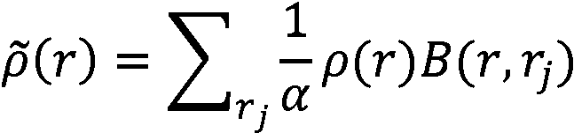
进一步地,模糊处理包括:
采用下式进行模糊处理:
其中,α=∑r
jB(r,r
j),B(r,r
j)=max{0,R
filt-||r-r
j||},R
filt为模糊半径,ρ(r)为初始掩模数据或更新后的掩模数据,即第一掩模数据,
 为模糊处理后的掩模数据,r为当前掩模数据中任意点的坐标,∑r
j表示在r坐标处遍历当前掩模数据中所有坐标点r
j进行求和。
为模糊处理后的掩模数据,r为当前掩模数据中任意点的坐标,∑r
j表示在r坐标处遍历当前掩模数据中所有坐标点r
j进行求和。
进一步地,投影处理包括:
采用下式进行二值化投影处理:

其中β为二值化参数,η为二值化阈值,
 为模糊处理后的掩模数据,
 为投影处理后的掩模数据,即第二掩模数据。
进一步地,计算成像数据与预期成像数据之间的成像误差包括:
采用下式计算成像误差F:
F=∑|P
a(x,y)-P
d(x,y)|
2/(m×n)×100%
其中,P
a(x,y)为当前掩模数据在预设的表面等离子体近场光刻的条件下对应的成像数据,P
d(x,y)为预期成像数据,(x,y)为成像数据中的坐标,m和n为成像数据对应的x与y方向的采样点数。
进一步地,根据正向场数据和伴随场数据计算成像误差相对于第一掩模数据的梯度矩阵包括:
采用下式计算梯度矩阵:
G(r)为梯度矩阵,n(r)为当前掩模数据的折射率分布,E
for(r)为正向场数据,E
adj(r)为伴随场数据。
进一步地,根据梯度矩阵对第一掩模数据进行更新包括:
采用下式计算更新后的掩模数据:
ρ
k+1(r)=ρ
k(r)+s·G(r)
其中,s为预先设定的优化步长,ρ
k(r)为当前掩模数据,ρ
k+1(r)为更新后的掩模数据,G(r)为梯度矩阵,k为当前迭代代数;其中,将更新后的掩模数据所有的像素值限定在[0,1]范围内,其中大于1的像素值设定为1,小于0的像素值设定为0,介于[0,1]范围内的像素值保持不 变。
进一步地,输出最终掩模图形包括:将当前掩模数据输出作为优化的掩模数据,采用边缘平滑方法提取优化的掩模数据的边缘并去除像素化锯齿后,输出最终掩模图形,其中,输出的优化的掩模数据为当前的第二掩模数据。
本公开还有一方面提供了一种表面等离子体近场光刻的方法,包括:获取第一掩模数据,对第一掩模数据进行模糊处理与投影处理,得到第二掩模数据;根据第二掩模数据和预设的表面等离子体近场光刻的条件进行正向计算,得到成像数据以及正向场数据;计算成像数据与预期成像数据之间的成像误差;对第二掩模数据进行伴随计算,得到伴随场数据;根据正向场数据和伴随场数据计算成像误差相对于第一掩模数据的梯度矩阵;根据梯度矩阵对第一掩模数据进行更新,重复上述步骤进行迭代计算,直至获得优化的掩模数据并输出最终掩模图形;根据最终掩模图形进行表面等离子体近场光刻。
本公开还有一方面提供了一种表面等离子体近场光刻掩模拓扑优化的系统,包括:掩模处理模块,用于获取第一掩模数据并对其进行模糊处理与投影处理,得到第二掩模数据;获取模块,用于根据第二掩模数据和预设的表面等离子体近场光刻的条件进行正向计算,得到成像数据以及正向场数据;成像误差计算模块,用于计算成像数据与预期成像数据之间的成像误差;伴随场数据计算模块,用于对第二掩模数据进行伴随计算,得到伴随场数据;梯度矩阵计算模块,用于根据正向场数据和伴随场数据计算成像误差相对于第一掩模数据的梯度矩阵;迭代计算模块,用于根据梯度矩阵对第一掩模数据进行更新,重复上述步骤进行迭代计算,直至获得优化的掩模数据并输出最终掩模图形。
本公开还有一方面提供了一种电子设备,包括:存储器,处理器及存储在存储器上并可在处理器上运行的计算机程序,处理器执行计算机程序时,使得处理器执行如前述的表面等离子体近场光刻掩模拓扑优化的方法。
本公开还有一方面提供了一种计算机可读存储介质,其上存储有计 算机程序,该计算机程序被处理器执行时,实现如前述的表面等离子体近场光刻掩模拓扑优化的方法。
本公开还有一方面提供了一种计算机程序产品,包括计算机程序,计算机程序被处理器执行时实现如前述的表面等离子体近场光刻掩模拓扑优化的方法。
本公开提供的一种表面等离子体近场光刻掩模拓扑优化的方法及系统,在正向计算的基础上引入伴随计算,得到优化梯度并对掩模拓扑形态进行调整补偿,以提高成像保真度与产品良率,不仅能够用于解决现有的近场光刻图案畸变问题,而且能够补偿光学邻近效应、杂散光效应和掩模阴影效应等亚波长电磁结构中的强耦合现象。本公开在掩模优化过程中,模糊滤除小于设定阈值的不能加工的微小结构,保证掩模图形任何部分的最小尺寸均大于或等于设定阈值,确保了掩模特征尺寸满足可制造性约束条件;还通过对像素化掩模图形中无法制造的边缘锯齿进行修正,进一步提高了掩模的可制造性。
为了更完整地理解本公开及其优势,现在将参考结合附图的以下描述,其中:
图1示意性示出了根据本公开实施例表面等离子体近场光刻掩模拓扑优化的方法的应用场景示意图;
图2示意性示出了根据本公开实施例的表面等离子体近场光刻掩模拓扑优化的方法流程图;
图3示意性示出了根据本公开实施例的表面等离子体近场光刻掩模拓扑优化的方法中获取第一掩模数据的方法流程图;
图4示意性示出了根据本公开实施例的表面等离子体近场光刻掩模拓扑优化的方法中进行伴随计算的方法流程图;
图5示意性示出了根据本公开一个示例性实施例的表面等离子体近 场光刻掩模拓扑优化的方法流程图;
图6示意性示出了根据本公开实施例一中的初始掩模数据、模糊处理后的掩模数据、投影处理后的掩模数据所对应的图形示意图;
图7示意性示出了根据本公开实施例一中的初始掩模数据及其对应光刻胶中的成像数据所对应的图形示意图;
图8示意性示出了根据本公开实施例一中掩模拓扑优化过程中第二掩模数据所对应的图形的迭代演变图;
图9示意性示出了根据本公开实施例一中优化得到的掩模数据及其对应光刻胶中的成像数据所对应的图形示意图;
图10示意性示出了根据本公开实施例二中采用结构101的基于本方法优化前后的掩模数据及其对应光刻胶中的成像数据所对应的图形示意图;
图11示意性示出了根据本公开实施例三中采用结构102的基于本方法优化前后的掩模数据及其对应光刻胶中的成像数据所对应的图形示意图;
图12示意性示出了根据本公开实施例的表面等离子体近场光刻掩模拓扑优化的系统的方框图;
图13示意性示出了根据本公开实施例的适于实现上文描述的方法的电子设备的方框图。
以下,将参照附图来描述本公开的实施例。但是应该理解,这些描述只是示例性的,而并非要限制本公开的范围。在下面的详细描述中,为便于解释,阐述了许多具体的细节以提供对本公开实施例的全面理解。然而,明显地,一个或多个实施例在没有这些具体细节的情况下也可以被实施。此外,在以下说明中,省略了对公知结构和技术的描述,以避免不必要地混淆本公开的概念。
在此使用的术语仅仅是为了描述具体实施例,而并非意在限制本公 开。在此使用的术语“包括”、“包含”等表明了所述特征、步骤、操作和/或部件的存在,但是并不排除存在或添加一个或多个其他特征、步骤、操作或部件。
在此使用的所有术语(包括技术和科学术语)具有本领域技术人员通常所理解的含义,除非另外定义。应注意,这里使用的术语应解释为具有与本说明书的上下文相一致的含义,而不应以理想化或过于刻板的方式来解释。
附图中示出了一些方框图和/或流程图。应理解,方框图和/或流程图中的一些方框或其组合可以由计算机程序指令来实现。这些计算机程序指令可以提供给通用计算机、专用计算机或其他可编程数据处理装置的处理器,从而这些指令在由该处理器执行时可以创建用于实现这些方框图和/或流程图中所说明的功能/操作的装置。本公开的技术可以硬件和/或软件(包括固件、微代码等)的形式来实现。另外,本公开的技术可以采取存储有指令的计算机可读存储介质上的计算机程序产品的形式,该计算机程序产品可供指令执行系统使用或者结合指令执行系统使用。
本公开所提供的基于伴随算法的针对表面等离子体近场光刻掩模的拓扑优化技术是一种重要的光刻分辨率增强技术,其通过优化掩模拓扑图形调制入射到光刻胶的光场强度分布,从而提高光刻系统的分辨率和图像保真度。掩模由像素化图形表征,具有高优化自由度,同时基于格林函数(Green’s function)的互易性,仅需要两次仿真计算即可评估掩模拓扑形状沿着光刻成像质量优化方向的梯度更新信息,大大降低了计算吞吐量、提升了优化速度。
在本公开中,为了便于说明,仅预期成像图形、初始掩模图形和最终掩模图形被称为图形,而拓扑优化中的计算过程和成像过程所得结果均被称为数据,可以理解的是,过程中的数据均能够对应输出相应的图形。
图1示意性示出了根据本公开实施例的可以应用于表面等离子体近场光刻掩模拓扑优化的方法的应用场景示意图。需要注意的是,图1所 示仅为可以应用本公开实施例的应用场景的示例,以帮助本领域技术人员理解本公开的技术内容,但并不意味着本公开实施例不可以用于其他设备、系统、环境或场景。
如图1所示,本公开实施例的表面等离子体近场光刻结构可以如101所示,包括掩模(SiO
2+Cr)、空气间隔层(Air)、金属层(Ag)、光刻胶(Pr)、金属反射层(Ag)和基底(SiO
2)的结构。表面等离子体近场光刻结构的界面图如102、103所示,光刻结构还可以包括掩模(SiO
2+Cr)、空气间隔层(Air)、光刻胶(Pr)、金属反射层(Ag)和基底(SiO
2)的结构(如102所示),也可以为包括掩模(SiO
2+Cr)、空气间隔层(Air)、金属层(Ag)、光刻胶(Pr)和基底(SiO
2)的结构(如103所示),只要能够实现表面等离子近场光刻的结构实际都可以。近场表面等离子体光刻中,将掩模上的图案转移至半导体芯片时,会表现出较差的对比度、较差的保真度和不均匀性。
基于此,本公开提供了基于伴随算法的针对表面等离子体近场光刻的掩模拓扑优化方法,能够针对实际需求提供效果更优良的掩模图形,补偿表面等离子体近场光刻系统中的光学邻近效应、杂散光效应、掩模阴影效应等亚波长电磁影响。
图2示意性示出了根据本公开实施例的表面等离子体近场光刻掩模拓扑优化的方法的流程图。
如图2所示,该表面等离子体近场光刻掩模拓扑优化的方法包括:
在操作S0,获取第一掩模数据并对其进行模糊处理与投影处理,得到第二掩模数据。
基于预期成像图形获取初始掩模图形,对该初始掩模图形进行像素化处理,得到初始掩模数据并得到预期成像数据。之后,将初始掩模数据或更新后的掩模数据作为第一掩模数据进行模糊处理与投影处理即可得到第二掩模数据。
在操作S1,根据第二掩模数据和预设的表面等离子体近场光刻的条件进行正向计算,得到成像数据以及正向场数据。
本步骤基于设定的表面等离子体近场光刻结构评估掩模的表面等 离子体近场成像性能。本步骤通过计算掩模图形在曝光光源激励源下在光刻胶中的成像性能,同时获得正向场数据用于后续伴随算法的梯度更新,此过程在本公开中即为正向计算或正向仿真。需要说明的是,光通过掩模之后在光刻胶中成像形成光强分布,即为成像数据;此处的正向场数据指的是掩模中的矢量电场数据。
在操作S2,计算成像数据与预期成像数据之间的成像误差。
本操作旨在计算当前成像的掩模在对应光刻胶中的成像图形与目标图形各像素之间的误差,具体通过数据计算实现。本公开设定的误差针对的是图形面积误差,其取值需依据所优化的掩模复杂程度、像素化网格大小、总体掩模大小等具体问题以及预期可容忍的图形畸变程度来选定,对于一般的集成电路掩模,常常需要优化后的成像面积误差控制在1%~3%以内。
在操作S3,对第二掩模数据进行伴随计算,得到伴随场数据。
基于本公开提出的伴随算法,对第二掩模数据进行伴随计算。本步骤在正向计算的基础上,将光刻胶中的成像监视器更换为特定伴随源的计算称为伴随计算,利用正向计算与伴随计算的结果得到梯度矩阵并更新掩模的优化算法称为伴随算法。需要说明的是,伴随场是基于一个给出的伴随激励源模拟计算得到的掩模中的矢量电场数据。
在操作S4,根据正向场数据和伴随场数据计算成像误差相对于第一掩模数据的梯度矩阵。
根据步骤S1中正向计算的结果和步骤S3中伴随计算的结果,计算得到每个像素对成像质量的贡献正负与大小,即得到梯度矩阵。
在操作S5,根据梯度矩阵对第一掩模数据进行更新,重复上述步骤进行迭代计算,直至获得优化的掩模数据并输出最终掩模图形。
根据步骤S4所得的梯度矩阵更新像素化的掩模数据,并循环进行步骤S0至S5,直到步骤S2中的成像性能满足设计指标。
本公开的方法在正向仿真的基础上,增加伴随仿真、梯度计算、掩模处理,基于先验物理信息快速迭代收敛,在提高优化速度的同时,获得更适应于表面等离子体光刻且效果更优良的掩模图形。
在上述实施例的基础上,计算成像数据与预期成像数据之间的成像误差包括:判断成像误差是否小于阈值或者当前累积迭代次数是否大于设定值:若是,则输出当前掩模数据作为优化的掩模数据;否则,继续进行迭代计算。
本公开中描述所使用的当前掩模数据代表当前迭代周期内相应步骤中所处理的掩模数据,可以是第一掩模数据,也可以是第二掩模数据,本领域技术人员能够基于不同的处理步骤了解当前掩模数据的含义。例如,在上面的步骤中,输出的当前掩模数据为当前迭代周期内满足判断依据的第二掩模数据,以便于实际掩模加工。
判断掩模图形的成像性能是否在预先设定的阈值内,或迭代次数是否超过最大迭代次数。该成像性能在本公开中用成像误差函数来表示,当小于阈值或迭代次数大于最大迭代次数时输出当前掩模数据作为优化后的掩模数据,否则进入步骤S0,进行迭代计算。对于一般的集成电路掩模,常常需要优化后的成像面积误差控制在1%~3%以内。本公开所需优化迭代次数常需要100~300代即可达到收敛最优值。
图3示意性示出了根据本公开实施例的表面等离子体近场光刻掩模拓扑优化的方法中获取第一掩模数据的方法流程图。
如图3所示,获取第一掩模的方法包括:
在操作S11,基于预期成像图形获取初始掩模图形。其中,预期成像图形即目标图形。
在操作S12,对初始掩模图形进行像素化处理,得到初始掩模数据并得到预期成像数据。其中,将初始掩模数据作为第一代迭代的第一掩模数据,预期成像数据与初始掩模数据相对应。
确定预期成像图形即目标图形后,基于该目标图形确定初始掩模图形,对该初始掩模图形进行像素化处理即可得到初始掩模数据。本步骤中定义图形的数据为二值化、像素化的矩阵。
具体地,预期成像数据为P
d(x,y),初始掩模数据作为第一代迭代的第一掩模数据ρ
1(r),为便于程序识别处理,将初始掩模图形栅格化分割为等间距的m×n的像素化网格,此时每个像素块的中心坐标取值为离 散值。
在操作S13,将初始掩模数据或更新后的掩模数据作为第一掩模数据进行模糊处理与投影处理,得到第二掩模数据。
本步骤中对初始掩模数据或更新后的掩模数据进行模糊处理,去除掉无法加工的小于最小设计规则的结构;再对模糊处理后的掩模数据进行二值化投影处理,得到满足实际物理模型的投影后的掩模数据,再进行后续计算,本步骤能够满足实际的掩模加工需求。
在上述实施例的基础上,对初始掩模数据ρ(r)或更新后的掩模数据进行线性模糊得到
 与二值化投影处理得到

线性模糊函数为:
其中,α=∑r
jB(r,r
j),B(r,r
j)=max{0,R
filt-||r-r
j||},R
filt为模糊半径,ρ(r)为初始掩模数据或更新后的掩模数据,即第一掩模数据,
 为模糊处理后的掩模数据,r为当前掩模数据中任意点的坐标,∑r
j表示在r坐标处遍历当前掩模数据中所有坐标点r
j进行求和。
为模糊处理后的掩模数据,r为当前掩模数据中任意点的坐标,∑r
j表示在r坐标处遍历当前掩模数据中所有坐标点r
j进行求和。
通过线性模糊处理,可实现去噪目的,使图像更光滑,同时也能使掩模分布更平滑,满足实际加工需求。
在上述实施例的基础上,二值化投影函数为:

其中β为二值化参数,η为二值化阈值,
 为模糊处理后的掩模数据,
 为投影处理后的掩模数据,即第二掩模数据。
经过二值化处理后的第二掩模数据的掩模矩阵数值将靠近0或1,满足实际掩模只有透明或不透明两个状态的物理意义。
在上述实施例的基础上,基于给定的表面等离子体光刻结构评估掩模图形的SPL成像性能,得到当前掩模数据在光刻胶中的成像数据。
本公开适用于任意掩模图形的优化,针对具有多个方向的复杂掩模图形,采用两次独立曝光的TM/TE偏振平面波作为正向计算的曝光光源激励源。因此,针对独立曝光TM/TE双偏振平面波光源,光刻胶中 的电场由时域有限差分算法可以严格计算,全波计算中会考虑亚波长结构间的复杂耦合及杂散光对空间像所造成的影响。当前掩模数据所对应的光刻胶中的成像结果即为电场的三个分量强度之和。显影过程可以由二值化函数Γ{·}表征,因此实际光刻成像数据表示为P
a=Γ{|E
TM(x,y)|
2+|E
TE(x,y)|
2-I
th},其中为I
th为光刻胶阈值。同时监测掩模中的矢量场,称为正向场E
for(r)。例如,702为实施例一中光线通过初始掩模图形并经由SPL系统后在光刻胶中的光强分布数据所对应的图形,703为二值化后成像数据所对应的曝光图形。
在上述实施例的基础上,本公开将成像误差函数F定义为:目标图形与当前掩模图形对应的光刻胶中成像图形各像素之差的平方和,具体通过数据计算,即F=∑|P
a(x,y)-P
d(x,y)|
2/(m×n)×100%,其中P
a(x,y)为掩模数据在预设的表面等离子体近场光刻的条件下对应的成像数据,P
d(x,y)为预期成像数据,(x,y)为成像数据中的坐标,m和n为成像数据对应的x和y方向的采样点数。
如果当前计算出成像误差函数值满足设定的阈值,或迭代次数大于最大迭代次数,则输出当前掩模数据作为优化的掩模数据,否则继续进行迭代计算。
图4示意性示出了根据本公开实施例的表面等离子体近场光刻掩模拓扑优化的方法中进行伴随计算的方法流程图。
如图4所示,对第二掩模数据进行伴随计算的方法包括:
在操作S41,采用伴随激励源进行仿真。
根据格林函数的互易性发现,保持当前的掩模数据
 不变的情况下,将成像监视器更换为如下的激励源进行仿真时,掩模上的伴随场E
adj(r)会携带优化所需的梯度信息,由于此时成像监视器与源位置调换,故称此为伴随计算。
不变的情况下,将成像监视器更换为如下的激励源进行仿真时,掩模上的伴随场E
adj(r)会携带优化所需的梯度信息,由于此时成像监视器与源位置调换,故称此为伴随计算。
给出的伴随激励源如下:
在操作S42,利用时域有限差分算法求解得到伴随场数据。
其中由于函数P
a(x,y)不满足柯西-黎曼条件,不利于梯度优化,故 此处采用实际成像图形的Sig(·)形函数近似的P′
a(x,y)表示当前成像图形,即
 伴随计算可以利用时域有限差分算法进行严格求解,监测掩模中的矢量场分量继而可得到伴随场E
adj(r)。
伴随计算可以利用时域有限差分算法进行严格求解,监测掩模中的矢量场分量继而可得到伴随场E
adj(r)。
在上述实施例的基础上,基于步骤S1所得正向场E
for(r)与步骤S3所得伴随场E
adj(r)的矢量电场数据,计算成像误差函数F相对于第一掩模数据ρ(r)的梯度矩阵
 其中n(r)为当前掩模数据的折射率分布,所得梯度矩阵代表当前掩模数据每个像素对成像质量的贡献正负与大小。
在上述实施例的基础上,根据上述步骤计算所得的梯度矩阵,对第一掩模数据进行一次更新,更新后的掩模矩阵ρ
k+1(r)由当前掩模矩阵ρ
k(r)与梯度矩阵组合获得,即ρ
k+1(r)=ρ
k(r)+s·G(r),其中k为当前迭代次数,s为预先设定的优化步长,s的经验值一般为0.01~0.1且可以随着迭代次数的增加而减少,以提高算法的收敛稳定性。
在更新后,将更新后的掩模数据所有像素值限定在[0,1]范围内,以保证掩模数据符合实际物理含义,其中大于1的像素值设定为1,小于0的像素值设定为0,介于[0,1]范围内的像素值保持不变,随后返回到步骤S1。
在上述实施例的基础上,输出当前掩模数据作为优化的掩模数据并输出最终掩模图形,包括:将当前掩模数据输出作为优化的掩模数据,采用边缘平滑方法提取优化的掩模数据的边缘并去除像素化锯齿后,输出最终掩模图形。其中,输出的优化的掩模数据为当前的第二掩模数据,以满足实际加工需求。
本公开将掩模的像素化密度参数作为优化参数,并通过拓扑优化最终确定优化掩模图形的形状。本公开中的掩模处理部分是将掩模图形分割为像素化的网格并得到像素化的掩模数据,每个像素可以用0-1之间的值表示,其中0表示透明的掩模,1表示不透明的掩模。在正向计算的基础上引入伴随计算,得到优化梯度并对掩模拓扑形态进行调整补偿,以提高成像保真度与产品良率。通过正向与伴随两次仿真计算,得到每一代的优化梯度方向,进而快速收敛到最优的掩模结构参数,同时实现 亚波长电磁邻近效应的补偿,得到较高的成像保真度。进一步地,还可以将前述获取的优化后的掩模用于表面等离子体近场光刻的方法中。
下面以一具体实施例对本方法的各步骤进行进一步说明,该方法的完整流程图如图5所示。
具体地,本公开的方法包括以下步骤:
步骤501:确定预期成像图形即目标图形,基于该目标图形确定初始掩模图形,对该初始掩模图形进行像素化处理,得到并输入初始掩模数据。本步骤中定义的掩模数据为二值化、像素化的矩阵。
将初始掩模数据定义为第一代迭代的第一掩模数据,而后迭代得到的更新后的掩模数据由上一代的第一掩模数据与梯度矩阵共同决定。
步骤502:对第一掩模数据,即初始掩模数据或更新后的掩模数据,进行模糊处理与投影处理得到第二掩模数据。本步骤中对初始掩模数据或更新后的掩模数据进行模糊处理,去除掉无法加工的小于最小设计规则的结构;再对模糊处理后的掩模数据进行二值化投影处理得到投影处理后的掩模数据,使其满足实际的物理模型。
步骤503:基于设定的表面等离子体近场光刻结构评估当前掩模数据的表面等离子体近场成像性能。本步骤通过计算当前掩模数据在曝光光源激励下在光刻胶中的成像性能,同时获得正向场数据用于后续伴随算法的梯度更新,这里掩模中的矢量电场分布值即正向场,此过程在本公开中即为正向计算或正向仿真,相当于前述S1。
步骤504:判断当前掩模数据的成像性能是否在预先设定的阈值内,或迭代次数是否超过最大迭代次数。该成像性能在本公开中用成像误差函数来表示,其定义为当前掩模数据在对应光刻胶中的成像图形与预期成像数据各像素之差的平方。当小于阈值或迭代次数大于最大迭代次数时跳到步骤508,否则进入步骤505,相当于前述S2。
步骤505:基于本公开提出的伴随算法,对第二掩模数据进行伴随计算。本步骤在正向计算的基础上,将光刻胶中的成像监视器更换为特定伴随源的计算称为伴随计算,伴随计算用于根据给出的伴随激励源模 拟计算得到虚拟的伴随场数据,利用正向计算与伴随计算的结果得到梯度更新掩模的优化算法称为伴随算法,相当于前述S3。
在步骤503、505中,正向计算与伴随计算可采用时域有限差分方法进行快速精准计算。
步骤506:根据步骤503中正向计算的结果和步骤505中伴随计算的结果,计算得到每个像素对成像质量的贡献正负与大小,即得到梯度矩阵,相当于前述S4。
步骤507:根据步骤506所得的梯度矩阵更新像素化的第一掩模数据得到更新后的掩模矩阵,并循环进行步骤502至507,直到步骤504中的成像性能满足设计指标,相当于前述S5。
步骤508:在优化结束后将当前掩模数据输出作为优化的掩模数据,采用边缘平滑方法提取边缘并去除无用且无法制作的像素化边缘锯齿,得到拓扑优化后的最终掩模图形。
按照上述步骤501~508,提供如下三个实施例:
实施例一:
图1中101为包括掩模、空气间隔层、金属层、光刻胶、金属反射层和基底的结构,本实施例中设置掩模厚度为50nm,空气间隔20nm,光刻胶上层金属层20nm,下层金属层70nm,光刻胶厚40nm。
图6中依次示出了601初始掩模数据ρ
1(r)、602模糊处理后的掩模数据
 603二值化投影处理后的掩模数据
 所对应的图形示意图
接下来评估当前掩模数据的SPL成像性能。如图7所示,701为初始掩模数据所对应的图形,对应于预期成像图形即目标图形,其中白色区域表示透明的部分,黑色表示非透明的掩模部分,其关键特征尺寸为70nm;702表示以701作为掩模图形通过SPL系统在光刻胶中的光强分布数据所对应的图形,703表示二值化后的曝光数据所对应的图形,其中光刻胶曝光二值化阈值设为2(I
th=2)。
计算得到成像误差为9.1911%,将成像误差的阈值设为1.5%,优化迭代次数设为250代,可见不满足设定的阈值。
根据步骤502至508,基于伴随场数据和正向场数据得到梯度矩阵 并进行第一掩模数据的像素值更新,反复进行迭代,第二掩模数据所对应图形的迭代演变参见图8中801~806所示,最终得到优化的掩模数据并输出得到最终掩模图形。
图9为采用本公开方法优化得到的掩模数据及其对应光刻胶中的成像数据所对应的图形示意图。901为采用本公开方法拓扑优化得到的掩模数据所对应的图形,902为以901作为掩模图形后通过SPL系统在光刻胶中的光强分布数据所对应的图形,903是902光强二值化后的曝光数据所对应的图形,其中光刻胶曝光二值化阈值为2,成像误差为1.6944%。
对比图7和图9可知,本公开的方法可以有效补偿SPL光刻系统中的光学邻近效应、杂散光效应、掩模阴影效应等近场强耦合影响,针对表面等离子体光刻的实际需求提供效果更优良的掩模图形。
实施例二:
图10表示在图1中101所示的SPL光刻结构中,采用本公开基于伴随算法的掩模拓扑优化方法优化前后的掩模数据以及对应光刻胶中的成像数据所对应的图形示意图,列出了三种掩模图形优化前后的情况。1001、1005、1009为初始掩模图形;1002、1006、1010为二值化曝光处理后所对应的光刻胶成像图形;1003、1007、1011为迭代完成后输出的最终掩模图形;1004、1008、1012为最终的成像图形。
其中,设置掩模厚度为40nm,空气间隔30nm,光刻胶上层金属层20nm,下层金属层50nm,光刻胶厚30nm,掩模的特征尺寸均为60nm。三种掩模图形经过本公开的优化后对应的成像误差值分别从12.3%、3%、6.8%降至2.1%、2.1%、2.7%。本实施例的成像误差阈值均设为2%,迭代次数为200代。
实施例三:
图11表示在图1中102所示的SPL光刻结构中,采用本公开基于伴随算法的掩模拓扑优化方法优化前后的掩模数据以及对应光刻胶中的成像数据所对应的图形示意图,列出了三种掩模图形优化前后的情况。1101、1105、1109为初始掩模图形;1102、1106、1110为二值化曝光处 理后所对应的光刻胶成像图形;1103、1107、1111为迭代完成后输出的最终掩模图形;1104、1108、1112为最终的成像图形。
其中设置掩模厚度为40nm,空气间隔20nm,光刻胶厚30nm,下层金属层70nm,掩模的特征尺寸均为70nm。三种掩模图形经过本公开的优化后对应的成像误差值分别从4.2%、6.1%、4.7%降至0.7%、0.6%、1.4%。本实施例的成像误差阈值均设为0.5%,迭代次数为120代。
图12示意性示出了根据本公开实施例的表面等离子体近场光刻掩模拓扑优化的系统的方框图。
如图12所示,该表面等离子体近场光刻掩模拓扑优化的系统1200包括:掩模处理模块1210、获取模块1220、成像误差计算模块1230、伴随场数据计算模块1240、梯度矩阵计算模块1250、迭代计算模块1260。
掩模处理模块1210,用于获取第一掩模数据并对其进行模糊处理与投影处理,得到第二掩模数据。根据本公开的实施例,掩模处理模块1210例如可以用于执行上文参考图2所描述的S1步骤,在此不再赘述。
获取模块1220,用于根据掩模数据和预设的表面等离子体近场光刻的条件进行正向计算,得到成像数据以及正向场数据;根据本公开的实施例,获取模块1220例如可以用于执行上文参考图2所描述的S2步骤,在此不再赘述。
成像误差计算模块1230,用于计算成像数据与预期成像数据之间的成像误差;根据本公开的实施例,该成像误差计算模块1230例如可以用于执行上文参考图2所描述的S3步骤,在此不再赘述。
伴随场数据计算模块1240,用于对掩模数据进行伴随计算,得到伴随场数据;根据本公开的实施例,该伴随场数据计算模块1240例如可以用于执行上文参考图2所描述的S4步骤,在此不再赘述。
梯度矩阵计算模块1250,用于根据正向场数据和伴随场数据计算成像误差相对于第一掩模数据的梯度矩阵;根据本公开的实施例,该梯度矩阵计算模块1250例如可以用于执行上文参考图2所描述的S5步骤,在此不再赘述。
迭代计算模块1260,用于根据梯度矩阵对第一掩模数据进行更新, 重复上述步骤进行迭代计算,直至获得优化的掩模数据并输出最终掩模图形;根据本公开的实施例,该迭代计算模块1260例如可以用于执行上文参考图2所描述的S6步骤,在此不再赘述。
需说明的是,根据本公开的实施例的模块、子模块、单元、子单元中的任意多个、或其中任意多个的至少部分功能可以在一个模块中实现。根据本公开实施例的模块、子模块、单元、子单元中的任意一个或多个可以被拆分成多个模块来实现。根据本公开实施例的模块、子模块、单元、子单元中的任意一个或多个可以至少被部分地实现为硬件电路,例如现场可编程门阵列(FPGA)、可编程逻辑阵列(PLA)、片上系统、基板上的系统、封装上的系统、专用集成电路(ASIC),或可以通过对电路进行集成或封装的任何其他的合理方式的硬件或固件来实现,或以软件、硬件以及固件三种实现方式中任意一种或以其中任意几种的适当组合来实现。或者,根据本公开实施例的模块、子模块、单元、子单元中的一个或多个可以至少被部分地实现为计算机程序模块,当该计算机程序模块被运行时,可以执行相应的功能。
例如,掩模处理模块1210、获取模块1220、成像误差计算模块1230、伴随场数据计算模块1240、梯度矩阵计算模块1250、迭代计算模块1260中的任意多个可以合并在一个模块中实现,或者其中的任意一个模块可以被拆分成多个模块。或者,这些模块中的一个或多个模块的至少部分功能可以与其他模块的至少部分功能相结合,并在一个模块中实现。根据本公开的实施例,掩模处理模块1210、获取模块1220、成像误差计算模块1230、伴随场数据计算模块1240、梯度矩阵计算模块1250、迭代计算模块1260中的至少一个可以至少被部分地实现为硬件电路,例如现场可编程门阵列(FPGA)、可编程逻辑阵列(PLA)、片上系统、基板上的系统、封装上的系统、专用集成电路(ASIC),或可以通过对电路进行集成或封装的任何其他的合理方式等硬件或固件来实现,或以软件、硬件以及固件三种实现方式中任意一种或以其中任意几种的适当组合来实现。或者,掩模处理模块1210、获取模块1220、成像误差计算模块1230、伴随场数据计算模块1240、梯度矩阵计算模块1250、迭代 计算模块1260中的至少一个可以至少被部分地实现为计算机程序模块,当该计算机程序模块被运行时,可以执行相应的功能。
图13示意性示出了根据本公开实施例的适于实现上文描述的方法的电子设备的方框图。图13示出的电子设备仅仅是一个示例,不应对本公开实施例的功能和使用范围带来任何限制。
如图13所示,本实施例中所描述的电子设备1300,包括:处理器1301,其可以根据存储在只读存储器(ROM)1302中的程序或者从存储部分1308加载到随机访问存储器(RAM)1303中的程序而执行各种适当的动作和处理。处理器1301例如可以包括通用微处理器(例如CPU)、指令集处理器和/或相关芯片组和/或专用微处理器(例如,专用集成电路(ASIC)),等等。处理器1301还可以包括用于缓存用途的板载存储器。处理器1301可以包括用于执行根据本公开实施例的方法流程的不同动作的单一处理单元或者是多个处理单元。
在RAM 1303中,存储有系统1300操作所需的各种程序和数据。处理器1301、ROM 1302以及RAM 1303通过总线1304彼此相连。处理器1301通过执行ROM 1302和/或RAM 1303中的程序来执行根据本公开实施例的方法流程的各种操作。需要注意,程序也可以存储在除ROM 1302和RAM 1303以外的一个或多个存储器中。处理器1301也可以通过执行存储在一个或多个存储器中的程序来执行根据本公开实施例的方法流程的各种操作。
根据本公开的实施例,电子设备1300还可以包括输入/输出(I/O)接口1305,输入/输出(I/O)接口1305也连接至总线1304。系统1300还可以包括连接至I/O接口1305的以下部件中的一项或多项:包括键盘、鼠标等的输入部分1306;包括诸如阴极射线管(CRT)、液晶显示器(LCD)等以及扬声器等的输出部分1307;包括硬盘等的存储部分1308;以及包括诸如LAN卡、调制解调器等的网络接口卡的通信部分1309。通信部分1309经由诸如因特网的网络执行通信处理。驱动器1310也根据需要连接至I/O接口1305。可拆卸介质1311,诸如磁盘、光盘、磁光盘、半导体存储器等等,根据需要安装在驱动器1310上,以便于从其上读 出的计算机程序根据需要被安装入存储部分1308。
根据本公开的实施例,根据本公开实施例的方法流程可以被实现为计算机软件程序。例如,本公开的实施例包括一种计算机程序产品,其包括承载在计算机可读存储介质上的计算机程序,该计算机程序包含用于执行流程图所示的方法的程序代码。在这样的实施例中,该计算机程序可以通过通信部分1309从网络上被下载和安装,和/或从可拆卸介质1311被安装。在该计算机程序被处理器1301执行时,执行本公开实施例的系统中限定的上述功能。根据本公开的实施例,上文描述的系统、设备、装置、模块、单元等可以通过计算机程序模块来实现。
本公开实施例还提供了一种计算机可读存储介质,该计算机可读存储介质可以是上述实施例中描述的设备/装置/系统中所包含的;也可以是单独存在,而未装配入该设备/装置/系统中。上述计算机可读存储介质承载有一个或者多个程序,当上述一个或者多个程序被执行时,实现根据本公开实施例的表面等离子体近场光刻掩模拓扑优化的方法。
根据本公开的实施例,计算机可读存储介质可以是非易失性的计算机可读存储介质,例如可以包括但不限于:便携式计算机磁盘、硬盘、随机访问存储器(RAM)、只读存储器(ROM)、可擦式可编程只读存储器(EPROM或闪存)、便携式紧凑磁盘只读存储器(CD-ROM)、光存储器件、磁存储器件、或者上述的任意合适的组合。在本公开的实施例中,计算机可读存储介质可以是任何包含或存储程序的有形介质,该程序可以被指令执行系统、装置或者器件使用或者与其结合使用。例如,根据本公开的实施例,计算机可读存储介质可以包括上文描述的ROM 1302和/或RAM 1303和/或ROM1302和RAM 1303以外的一个或多个存储器。
本公开的实施例还包括一种计算机程序产品,其包括计算机程序,该计算机程序包含用于执行流程图所示的方法的程序代码。当计算机程序产品在计算机系统中运行时,该程序代码用于使计算机系统实现本公开实施例所提供的表面等离子体近场光刻掩模拓扑优化的方法。
在该计算机程序被处理器1301执行时执行本公开实施例的系统/装置中限定的上述功能。根据本公开的实施例,上文描述的系统、装置、模块、单元等可以通过计算机程序模块来实现。
在一种实施例中,该计算机程序可以依托于光存储器件、磁存储器件等有形存储介质。在另一种实施例中,该计算机程序也可以在网络介质上以信号的形式进行传输、分发,并通过通信部分1309被下载和安装,和/或从可拆卸介质1311被安装。该计算机程序包含的程序代码可以用任何适当的网络介质传输,包括但不限于:无线、有线等等,或者上述的任意合适的组合。
在这样的实施例中,该计算机程序可以通过通信部分1309从网络上被下载和安装,和/或从可拆卸介质1311被安装。在该计算机程序被处理器1301执行时,执行本公开实施例的系统中限定的上述功能。根据本公开的实施例,上文描述的系统、设备、装置、模块、单元等可以通过计算机程序模块来实现。
根据本公开的实施例,可以以一种或多种程序设计语言的任意组合来编写用于执行本公开实施例提供的计算机程序的程序代码,具体地,可以利用高级过程和/或面向对象的编程语言、和/或汇编/机器语言来实施这些计算程序。程序设计语言包括但不限于诸如Java,C++,python,“C”语言或类似的程序设计语言。程序代码可以完全地在用户计算设备上执行、部分地在用户设备上执行、部分在远程计算设备上执行、或者完全在远程计算设备或服务器上执行。在涉及远程计算设备的情形中,远程计算设备可以通过任意种类的网络,包括局域网(LAN)或广域网(WAN),连接到用户计算设备,或者,可以连接到外部计算设备(例如利用因特网服务提供商来通过因特网连接)。
需要说明的是,在本公开各个实施例中的各功能模块可以集成在一个处理模块中,也可以是各个模块单独物理存在,也可以两个或两个以上模块集成在一个模块中。上述集成的模块既可以采用硬件的形式实现,也可以采用软件功能模块的形式实现。集成的模块如果以软件功能模块的形式实现并作为独立的产品销售或使用时,可以存储在一个计算机可 读取存储介质中。基于这样的理解,本公开的技术方案本质上或者说对现有技术做出贡献的部分或者该技术方案的全部或部分可以以软件产品的形式体现出来。
附图中的流程图和框图,图示了按照本公开各种实施例的系统、方法和计算机程序产品的可能实现的体系架构、功能和操作。在这点上,流程图或框图中的每个方框可以代表一个模块、程序段、或代码的一部分,上述模块、程序段、或代码的一部分包含一个或多个用于实现规定的逻辑功能的可执行指令。也应当注意,在有些作为替换的实现中,方框中所标注的功能也可以以不同于附图中所标注的顺序发生。例如,两个接连地表示的方框实际上可以基本并行地执行,它们有时也可以按相反的顺序执行,这依所涉及的功能而定。也要注意的是,框图或流程图中的每个方框、以及框图或流程图中的方框的组合,可以用执行规定的功能或操作的专用的基于硬件的系统来实现,或者可以用专用硬件与计算机指令的组合来实现。
本领域技术人员可以理解,本公开的各个实施例和/或权利要求中记载的特征可以进行多种组合和/或结合,即使这样的组合或结合没有明确记载于本公开中。特别地,在不脱离本公开精神和教导的情况下,本公开的各个实施例和/或权利要求中记载的特征可以进行多种组合和/或结合。所有这些组合和/或结合均落入本公开的范围。
尽管已经参照本公开的特定示例性实施例示出并描述了本公开,但是本领域技术人员应该理解,在不背离所附权利要求及其等同物限定的本公开的精神和范围的情况下,可以对本公开进行形式和细节上的多种改变。因此,本公开的范围不应该限于上述实施例,而是应该不仅由所附权利要求来进行确定,还由所附权利要求的等同物来进行限定。
Claims (16)
- 一种表面等离子体近场光刻掩模拓扑优化的方法,其特征在于,包括:获取第一掩模数据并对其进行模糊处理与投影处理,得到第二掩模数据;根据所述第二掩模数据和预设的表面等离子体近场光刻的条件进行正向计算,得到成像数据以及正向场数据;计算所述成像数据与预期成像数据之间的成像误差;对所述第二掩模数据进行伴随计算,得到伴随场数据;根据所述正向场数据和所述伴随场数据计算所述成像误差相对于所述第一掩模数据的梯度矩阵;根据所述梯度矩阵对所述第一掩模数据进行更新,重复上述步骤进行迭代计算,直至获得优化的掩模数据并输出最终掩模图形。
- 根据权利要求1所述的表面等离子体近场光刻掩模拓扑优化的方法,其特征在于,所述计算所述成像数据与预期成像数据之间的成像误差包括:判断所述成像误差是否小于阈值或者当前累积迭代次数是否大于设定值:若是,则输出当前掩模数据作为优化的掩模数据;否则,继续进行迭代计算。
- 根据权利要求1所述的表面等离子体近场光刻掩模拓扑优化的方法,其特征在于,所述正向计算包括:采用曝光光源激励源进行仿真;利用时域有限差分算法求解得到所述成像数据和正向场数据。
- 根据权利要求1所述的表面等离子体近场光刻掩模拓扑优化的方法,其特征在于,所述伴随计算包括:采用伴随激励源进行仿真;利用时域有限差分算法求解得到所述伴随场数据。
- 根据权利要求1所述的表面等离子体近场光刻掩模拓扑优化的方法,其特征在于,所述获取第一掩模数据包括:基于预期成像图形获取初始掩模图形;对所述初始掩模图形进行像素化处理,得到初始掩模数据并得到预期成像数据;将所述初始掩模数据或更新后的掩模数据作为第一掩模数据进行模糊处理与投影处理。
- 根据权利要求1所述的表面等离子体近场光刻掩模拓扑优化的方法,其特征在于,所述模糊处理包括:采用下式进行模糊处理:
 其中,R filt为模糊半径,ρ(r)为初始掩模数据或更新后的掩模数据,即第一掩模数据,
 为模糊处理后的掩模数据,r为当前掩模数据中任意点的坐标,
 表示在r坐标处遍历当前掩模数据中所有坐标点r j进行求和。
- 根据权利要求1所述的表面等离子体近场光刻掩模拓扑优化的方法,其特征在于,所述投影处理包括:采用下式进行二值化投影处理:
 其中β为二值化参数,η为二值化阈值,为模糊处理后的掩模数据,
 为投影处理后的掩模数据,即第二掩模数据。
- 根据权利要求1所述的表面等离子体近场光刻掩模拓扑优化的方法,其特征在于,所述计算所述成像数据与预期成像数据之间的成像误差包括:采用下式计算所述成像误差F:F=∑|P a(x,y)-P d(x,y)| 2/(m×n)×100%其中,P a(x,y)为当前掩模数据在预设的表面等离子体近场光刻的条件下对应的成像数据,P d(x,y)为所述预期成像数据,(x,y)为成像数据中的坐标,m和n为成像数据对应的x与y方向的采样点数。
- 根据权利要求8所述的表面等离子体近场光刻掩模拓扑优化的方法,其特征在于,所述根据所述正向场数据和所述伴随场数据计算所述成像误差相对于所述第一掩模数据的梯度矩阵包括:采用下式计算所述梯度矩阵:
 G(r)为所述梯度矩阵,n(r)为当前掩模数据的折射率分布,E for(r)为所述正向场数据,E adj(r)为所述伴随场数据。
 - 根据权利要求9所述的表面等离子体近场光刻掩模拓扑优化的方法,其特征在于,所述根据所述梯度矩阵对所述第一掩模数据进行更新包括:采用下式计算更新后的掩模数据:ρ k+1(r)=ρ k(r)+s·G(r)其中,s为预先设定的优化步长,ρ k(r)为当前掩模数据,ρ k+1(r)为更新后的掩模数据,G(r)为所述梯度矩阵,k为当前迭代代数;其中,将更新后的掩模数据所有的像素值限定在[0,1]范围内,其中大于1的像素值设定为1,小于0的像素值设定为0,介于[0,1]范围内的像素值保持不变。
- 根据权利要求1所述的表面等离子体近场光刻掩模拓扑优化的方法,其特征在于,所述输出最终掩模图形包括:将当前掩模数据输出作为优化的掩模数据,采用边缘平滑方法提取所述优化的掩模数据的边缘并去除像素化锯齿后,输出最终掩模图形,其中,输出的所述优化的掩模数据为当前的第二掩模数据。
- 一种表面等离子体近场光刻的方法,其特征在于,包括:获取第一掩模数据,对所述第一掩模数据进行模糊处理与投影处理,得到第二掩模数据;根据第二掩模数据和预设的表面等离子体近场光刻的条件进行正向计算,得到成像数据以及正向场数据;计算所述成像数据与预期成像数据之间的成像误差;对所述第二掩模数据进行伴随计算,得到伴随场数据;根据所述正向场数据和所述伴随场数据计算所述成像误差相对于 所述第一掩模数据的梯度矩阵;根据所述梯度矩阵对所述第一掩模数据进行更新,重复上述步骤进行迭代计算,直至获得优化的掩模数据并输出最终掩模图形;根据所述最终掩模图形进行表面等离子体近场光刻。
- 一种表面等离子体近场光刻掩模拓扑优化的系统,其特征在于,包括:掩模处理模块,用于获取第一掩模数据并对其进行模糊处理与投影处理,得到第二掩模数据;获取模块,用于根据第二掩模数据和预设的表面等离子体近场光刻的条件进行正向计算,得到成像数据以及正向场数据;成像误差计算模块,用于计算所述成像数据与预期成像数据之间的成像误差;伴随场数据计算模块,用于对所述第二掩模数据进行伴随计算,得到伴随场数据;梯度矩阵计算模块,用于根据所述正向场数据和所述伴随场数据计算所述成像误差相对于所述第一掩模数据的梯度矩阵;迭代计算模块,用于根据所述梯度矩阵对所述第一掩模数据进行更新,重复上述步骤进行迭代计算,直至获得优化的掩模数据并输出最终掩模图形。
- 一种电子设备,包括:处理器;存储器,其存储有计算机可执行程序,该程序在被所述处理器执行时,使得所述处理器执行如权利要求1~11中任意一项所述的表面等离子体近场光刻掩模拓扑优化的方法。
- 一种计算机可读存储介质,其上存储有计算机程序,其特征在于,该程序被处理器执行时实现如权利要求1~11中任意一项所述的表面等离子体近场光刻掩模拓扑优化的方法。
- 一种计算机程序产品,包括计算机程序,所述计算机程序被处理器执行时实现根据权利要求1~11中任意一项所述的表面等离子体近 场光刻掩模拓扑优化的方法。
Priority Applications (3)
| Application Number | Priority Date | Filing Date | Title |
|---|---|---|---|
| US18/575,532 US12092960B2 (en) | 2021-10-14 | 2021-10-14 | Mask topology optimization method and system for surface plasmon near-field photolithography |
| JP2023579753A JP7558433B2 (ja) | 2021-10-14 | 2021-10-14 | 表面プラズモン近接場リソグラフィにおけるマスクのトポロジ最適化の方法及びシステム |
| PCT/CN2021/123793 WO2023060505A1 (zh) | 2021-10-14 | 2021-10-14 | 一种表面等离子体近场光刻掩模拓扑优化的方法及系统 |
Applications Claiming Priority (1)
| Application Number | Priority Date | Filing Date | Title |
|---|---|---|---|
| PCT/CN2021/123793 WO2023060505A1 (zh) | 2021-10-14 | 2021-10-14 | 一种表面等离子体近场光刻掩模拓扑优化的方法及系统 |
Publications (1)
| Publication Number | Publication Date |
|---|---|
| WO2023060505A1 true WO2023060505A1 (zh) | 2023-04-20 |
Family
ID=85987224
Family Applications (1)
| Application Number | Title | Priority Date | Filing Date |
|---|---|---|---|
| PCT/CN2021/123793 WO2023060505A1 (zh) | 2021-10-14 | 2021-10-14 | 一种表面等离子体近场光刻掩模拓扑优化的方法及系统 |
Country Status (3)
| Country | Link |
|---|---|
| US (1) | US12092960B2 (zh) |
| JP (1) | JP7558433B2 (zh) |
| WO (1) | WO2023060505A1 (zh) |
Cited By (3)
| Publication number | Priority date | Publication date | Assignee | Title |
|---|---|---|---|---|
| CN116819903A (zh) * | 2023-07-11 | 2023-09-29 | 安徽国芯智能装备有限公司 | 一种直写式光刻机的曝光及图形补偿方法 |
| CN117452779A (zh) * | 2023-12-04 | 2024-01-26 | 武汉宇微光学软件有限公司 | 一种计算光刻非线性系统的建模、标定方法和装置 |
| CN117454831A (zh) * | 2023-12-05 | 2024-01-26 | 武汉宇微光学软件有限公司 | 一种掩模版图形优化方法、系统及电子设备 |
Citations (4)
| Publication number | Priority date | Publication date | Assignee | Title |
|---|---|---|---|---|
| CN104635434A (zh) * | 2015-01-29 | 2015-05-20 | 北京理工大学 | 一种极紫外光刻掩模优化方法 |
| CN108535952A (zh) * | 2018-04-09 | 2018-09-14 | 北京理工大学 | 一种基于模型驱动卷积神经网络的计算光刻方法 |
| CN110678961A (zh) * | 2017-05-26 | 2020-01-10 | Asml美国有限责任公司 | 在光学光刻中模拟近场图像 |
| US10725373B1 (en) * | 2016-10-21 | 2020-07-28 | Iowa State University Research Foundation, Inc. | Nano-patterning methods including: (1) patterning of nanophotonic structures at optical fiber tip for refractive index sensing and (2) plasmonic crystal incorporating graphene oxide gas sensor for detection of volatile organic compounds |
Family Cites Families (9)
| Publication number | Priority date | Publication date | Assignee | Title |
|---|---|---|---|---|
| JP2001308002A (ja) | 2000-02-15 | 2001-11-02 | Canon Inc | フォトマスクを用いたパターン作製方法、及びパターン作製装置 |
| JP3715973B2 (ja) | 2002-05-07 | 2005-11-16 | キヤノン株式会社 | 近接場光露光用のフォトマスク、該フォトマスクを用いたパターン作製方法およびパターン作製装置 |
| JP2005353629A (ja) | 2004-06-08 | 2005-12-22 | Canon Inc | 近接場露光に用いるマスク、該マスクを用いた近接場光の強度分布制御方法、基板の製造方法および露光装置 |
| JP4574250B2 (ja) | 2004-06-30 | 2010-11-04 | キヤノン株式会社 | フォトマスク |
| JP2008021869A (ja) | 2006-07-13 | 2008-01-31 | Ricoh Co Ltd | プラズモン共鳴リソグラフィおよびリソグラム |
| EP2544218B1 (en) | 2010-03-02 | 2016-02-10 | National University Corporation Hokkaido University | Process for production of photoresist pattern |
| JP6399751B2 (ja) | 2013-12-25 | 2018-10-03 | キヤノン株式会社 | マスクパターン作成方法、プログラム、マスク製造方法、露光方法及び物品製造方法 |
| CN111381435B (zh) | 2018-12-28 | 2022-11-04 | 国家纳米科学中心 | 一种表面等离激元掩模板 |
| TWI738169B (zh) * | 2019-01-29 | 2021-09-01 | 荷蘭商Asml荷蘭公司 | 用於為佈局圖案化程序判定訓練圖案之方法及相關的電腦程式產品 |
-
2021
- 2021-10-14 WO PCT/CN2021/123793 patent/WO2023060505A1/zh active Application Filing
- 2021-10-14 US US18/575,532 patent/US12092960B2/en active Active
- 2021-10-14 JP JP2023579753A patent/JP7558433B2/ja active Active
Patent Citations (4)
| Publication number | Priority date | Publication date | Assignee | Title |
|---|---|---|---|---|
| CN104635434A (zh) * | 2015-01-29 | 2015-05-20 | 北京理工大学 | 一种极紫外光刻掩模优化方法 |
| US10725373B1 (en) * | 2016-10-21 | 2020-07-28 | Iowa State University Research Foundation, Inc. | Nano-patterning methods including: (1) patterning of nanophotonic structures at optical fiber tip for refractive index sensing and (2) plasmonic crystal incorporating graphene oxide gas sensor for detection of volatile organic compounds |
| CN110678961A (zh) * | 2017-05-26 | 2020-01-10 | Asml美国有限责任公司 | 在光学光刻中模拟近场图像 |
| CN108535952A (zh) * | 2018-04-09 | 2018-09-14 | 北京理工大学 | 一种基于模型驱动卷积神经网络的计算光刻方法 |
Cited By (6)
| Publication number | Priority date | Publication date | Assignee | Title |
|---|---|---|---|---|
| CN116819903A (zh) * | 2023-07-11 | 2023-09-29 | 安徽国芯智能装备有限公司 | 一种直写式光刻机的曝光及图形补偿方法 |
| CN116819903B (zh) * | 2023-07-11 | 2024-06-04 | 安徽国芯智能装备有限公司 | 一种直写式光刻机的曝光及图形补偿方法 |
| CN117452779A (zh) * | 2023-12-04 | 2024-01-26 | 武汉宇微光学软件有限公司 | 一种计算光刻非线性系统的建模、标定方法和装置 |
| CN117452779B (zh) * | 2023-12-04 | 2024-03-19 | 武汉宇微光学软件有限公司 | 一种计算光刻非线性系统的建模、标定方法和装置 |
| CN117454831A (zh) * | 2023-12-05 | 2024-01-26 | 武汉宇微光学软件有限公司 | 一种掩模版图形优化方法、系统及电子设备 |
| CN117454831B (zh) * | 2023-12-05 | 2024-04-02 | 武汉宇微光学软件有限公司 | 一种掩模版图形优化方法、系统及电子设备 |
Also Published As
| Publication number | Publication date |
|---|---|
| US12092960B2 (en) | 2024-09-17 |
| JP2024526224A (ja) | 2024-07-17 |
| JP7558433B2 (ja) | 2024-09-30 |
| US20240264535A1 (en) | 2024-08-08 |
Similar Documents
| Publication | Publication Date | Title |
|---|---|---|
| WO2023060505A1 (zh) | 一种表面等离子体近场光刻掩模拓扑优化的方法及系统 | |
| CN110678961B (zh) | 在光学光刻中模拟近场图像 | |
| US10909294B2 (en) | Modeling of a design in reticle enhancement technology | |
| JP7497537B1 (ja) | レベルセットアルゴリズムに基づく超解像リソグラフィのリバース光近接効果補正方法 | |
| US8918743B1 (en) | Edge-based full chip mask topography modeling | |
| CN103926802B (zh) | 光刻机光源与掩模的联合优化方法 | |
| US8082524B2 (en) | Mask patterns for use in multiple-exposure lithography | |
| CN106125511B (zh) | 基于矢量成像模型的低误差敏感度多目标光源‑掩模优化方法 | |
| CN105573066B (zh) | 光刻机掩模的优化方法 | |
| US8082525B2 (en) | Technique for correcting hotspots in mask patterns and write patterns | |
| CN114815496B (zh) | 应用于超分辨光刻的像素化光学邻近效应修正方法及系统 | |
| WO2007041600A2 (en) | Mask-pattern determination using topology types | |
| CN104635434A (zh) | 一种极紫外光刻掩模优化方法 | |
| TWI795566B (zh) | 用於執行光學近接校正的方法及使用光學近接校正製造遮罩的方法 | |
| CN113962185B (zh) | 一种表面等离子体近场光刻掩模拓扑优化的方法及系统 | |
| WO2019209591A1 (en) | Mask pattern generation based on fast marching method | |
| US10571799B1 (en) | Hessian-free calculation of product of Hessian matrix and vector for lithography optimization | |
| CN113189845A (zh) | 基于人工期望的目标图案掩膜优化方法 | |
| CN117192889A (zh) | 超分辨光刻中工艺窗口相关的光学邻近效应修正方法 | |
| CN115712227A (zh) | 基于倏逝波场强衰减特性调制式的光学邻近效应校正方法及装置 | |
| CN109709772A (zh) | 一种基于加速算子分裂的半隐式光源掩膜协同优化方法 | |
| US20240086607A1 (en) | Modeling of a design in reticle enhancement technology | |
| CN117331288A (zh) | 对线栅图形进行双重图形成像的修正方法及光刻方法 | |
| CN117807955A (zh) | 一种极紫外光刻掩模优化方法及系统 | |
| KR100989746B1 (ko) | 광학 파라미터와 리스크 함수를 이용한 광학적 근접 보정 검증 방법 |
Legal Events
| Date | Code | Title | Description |
|---|---|---|---|
| 121 | Ep: the epo has been informed by wipo that ep was designated in this application |
Ref document number: 21960242 Country of ref document: EP Kind code of ref document: A1 |
|
| ENP | Entry into the national phase |
Ref document number: 2023579753 Country of ref document: JP Kind code of ref document: A |
|
| NENP | Non-entry into the national phase |
Ref country code: DE |
|
| 122 | Ep: pct application non-entry in european phase |
Ref document number: 21960242 Country of ref document: EP Kind code of ref document: A1 |