WO2023058319A1 - Radio wave reflection element and radio wave reflection plate - Google Patents
Radio wave reflection element and radio wave reflection plate Download PDFInfo
- Publication number
- WO2023058319A1 WO2023058319A1 PCT/JP2022/030215 JP2022030215W WO2023058319A1 WO 2023058319 A1 WO2023058319 A1 WO 2023058319A1 JP 2022030215 W JP2022030215 W JP 2022030215W WO 2023058319 A1 WO2023058319 A1 WO 2023058319A1
- Authority
- WO
- WIPO (PCT)
- Prior art keywords
- alignment film
- radio wave
- electrode
- liquid crystal
- crystal layer
- Prior art date
- Legal status (The legal status is an assumption and is not a legal conclusion. Google has not performed a legal analysis and makes no representation as to the accuracy of the status listed.)
- Ceased
Links
Images


Classifications
-
- G—PHYSICS
- G02—OPTICS
- G02F—OPTICAL DEVICES OR ARRANGEMENTS FOR THE CONTROL OF LIGHT BY MODIFICATION OF THE OPTICAL PROPERTIES OF THE MEDIA OF THE ELEMENTS INVOLVED THEREIN; NON-LINEAR OPTICS; FREQUENCY-CHANGING OF LIGHT; OPTICAL LOGIC ELEMENTS; OPTICAL ANALOGUE/DIGITAL CONVERTERS
- G02F1/00—Devices or arrangements for the control of the intensity, colour, phase, polarisation or direction of light arriving from an independent light source, e.g. switching, gating or modulating; Non-linear optics
- G02F1/01—Devices or arrangements for the control of the intensity, colour, phase, polarisation or direction of light arriving from an independent light source, e.g. switching, gating or modulating; Non-linear optics for the control of the intensity, phase, polarisation or colour
- G02F1/13—Devices or arrangements for the control of the intensity, colour, phase, polarisation or direction of light arriving from an independent light source, e.g. switching, gating or modulating; Non-linear optics for the control of the intensity, phase, polarisation or colour based on liquid crystals, e.g. single liquid crystal display cells
- G02F1/133—Constructional arrangements; Operation of liquid crystal cells; Circuit arrangements
- G02F1/1333—Constructional arrangements; Manufacturing methods
- G02F1/1337—Surface-induced orientation of the liquid crystal molecules, e.g. by alignment layers
-
- G—PHYSICS
- G02—OPTICS
- G02F—OPTICAL DEVICES OR ARRANGEMENTS FOR THE CONTROL OF LIGHT BY MODIFICATION OF THE OPTICAL PROPERTIES OF THE MEDIA OF THE ELEMENTS INVOLVED THEREIN; NON-LINEAR OPTICS; FREQUENCY-CHANGING OF LIGHT; OPTICAL LOGIC ELEMENTS; OPTICAL ANALOGUE/DIGITAL CONVERTERS
- G02F1/00—Devices or arrangements for the control of the intensity, colour, phase, polarisation or direction of light arriving from an independent light source, e.g. switching, gating or modulating; Non-linear optics
- G02F1/01—Devices or arrangements for the control of the intensity, colour, phase, polarisation or direction of light arriving from an independent light source, e.g. switching, gating or modulating; Non-linear optics for the control of the intensity, phase, polarisation or colour
- G02F1/13—Devices or arrangements for the control of the intensity, colour, phase, polarisation or direction of light arriving from an independent light source, e.g. switching, gating or modulating; Non-linear optics for the control of the intensity, phase, polarisation or colour based on liquid crystals, e.g. single liquid crystal display cells
-
- H—ELECTRICITY
- H01—ELECTRIC ELEMENTS
- H01Q—ANTENNAS, i.e. RADIO AERIALS
- H01Q15/00—Devices for reflection, refraction, diffraction or polarisation of waves radiated from an antenna, e.g. quasi-optical devices
- H01Q15/14—Reflecting surfaces; Equivalent structures
- H01Q15/148—Reflecting surfaces; Equivalent structures with means for varying the reflecting properties
-
- H—ELECTRICITY
- H01—ELECTRIC ELEMENTS
- H01Q—ANTENNAS, i.e. RADIO AERIALS
- H01Q3/00—Arrangements for changing or varying the orientation or the shape of the directional pattern of the waves radiated from an antenna or antenna system
- H01Q3/26—Arrangements for changing or varying the orientation or the shape of the directional pattern of the waves radiated from an antenna or antenna system varying the relative phase or relative amplitude of energisation between two or more active radiating elements; varying the distribution of energy across a radiating aperture
- H01Q3/30—Arrangements for changing or varying the orientation or the shape of the directional pattern of the waves radiated from an antenna or antenna system varying the relative phase or relative amplitude of energisation between two or more active radiating elements; varying the distribution of energy across a radiating aperture varying the relative phase between the radiating elements of an array
- H01Q3/34—Arrangements for changing or varying the orientation or the shape of the directional pattern of the waves radiated from an antenna or antenna system varying the relative phase or relative amplitude of energisation between two or more active radiating elements; varying the distribution of energy across a radiating aperture varying the relative phase between the radiating elements of an array by electrical means
- H01Q3/36—Arrangements for changing or varying the orientation or the shape of the directional pattern of the waves radiated from an antenna or antenna system varying the relative phase or relative amplitude of energisation between two or more active radiating elements; varying the distribution of energy across a radiating aperture varying the relative phase between the radiating elements of an array by electrical means with variable phase-shifters
-
- H—ELECTRICITY
- H01—ELECTRIC ELEMENTS
- H01Q—ANTENNAS, i.e. RADIO AERIALS
- H01Q3/00—Arrangements for changing or varying the orientation or the shape of the directional pattern of the waves radiated from an antenna or antenna system
- H01Q3/44—Arrangements for changing or varying the orientation or the shape of the directional pattern of the waves radiated from an antenna or antenna system varying the electric or magnetic characteristics of reflecting, refracting, or diffracting devices associated with the radiating element
- H01Q3/46—Active lenses or reflecting arrays
-
- G—PHYSICS
- G02—OPTICS
- G02F—OPTICAL DEVICES OR ARRANGEMENTS FOR THE CONTROL OF LIGHT BY MODIFICATION OF THE OPTICAL PROPERTIES OF THE MEDIA OF THE ELEMENTS INVOLVED THEREIN; NON-LINEAR OPTICS; FREQUENCY-CHANGING OF LIGHT; OPTICAL LOGIC ELEMENTS; OPTICAL ANALOGUE/DIGITAL CONVERTERS
- G02F1/00—Devices or arrangements for the control of the intensity, colour, phase, polarisation or direction of light arriving from an independent light source, e.g. switching, gating or modulating; Non-linear optics
- G02F1/01—Devices or arrangements for the control of the intensity, colour, phase, polarisation or direction of light arriving from an independent light source, e.g. switching, gating or modulating; Non-linear optics for the control of the intensity, phase, polarisation or colour
- G02F1/13—Devices or arrangements for the control of the intensity, colour, phase, polarisation or direction of light arriving from an independent light source, e.g. switching, gating or modulating; Non-linear optics for the control of the intensity, phase, polarisation or colour based on liquid crystals, e.g. single liquid crystal display cells
- G02F1/133—Constructional arrangements; Operation of liquid crystal cells; Circuit arrangements
- G02F1/1333—Constructional arrangements; Manufacturing methods
- G02F1/1337—Surface-induced orientation of the liquid crystal molecules, e.g. by alignment layers
- G02F1/133753—Surface-induced orientation of the liquid crystal molecules, e.g. by alignment layers with different alignment orientations or pretilt angles on a same surface, e.g. for grey scale or improved viewing angle
- G02F1/133757—Surface-induced orientation of the liquid crystal molecules, e.g. by alignment layers with different alignment orientations or pretilt angles on a same surface, e.g. for grey scale or improved viewing angle with different alignment orientations
-
- G—PHYSICS
- G02—OPTICS
- G02F—OPTICAL DEVICES OR ARRANGEMENTS FOR THE CONTROL OF LIGHT BY MODIFICATION OF THE OPTICAL PROPERTIES OF THE MEDIA OF THE ELEMENTS INVOLVED THEREIN; NON-LINEAR OPTICS; FREQUENCY-CHANGING OF LIGHT; OPTICAL LOGIC ELEMENTS; OPTICAL ANALOGUE/DIGITAL CONVERTERS
- G02F1/00—Devices or arrangements for the control of the intensity, colour, phase, polarisation or direction of light arriving from an independent light source, e.g. switching, gating or modulating; Non-linear optics
- G02F1/01—Devices or arrangements for the control of the intensity, colour, phase, polarisation or direction of light arriving from an independent light source, e.g. switching, gating or modulating; Non-linear optics for the control of the intensity, phase, polarisation or colour
- G02F1/13—Devices or arrangements for the control of the intensity, colour, phase, polarisation or direction of light arriving from an independent light source, e.g. switching, gating or modulating; Non-linear optics for the control of the intensity, phase, polarisation or colour based on liquid crystals, e.g. single liquid crystal display cells
- G02F1/133—Constructional arrangements; Operation of liquid crystal cells; Circuit arrangements
- G02F1/1333—Constructional arrangements; Manufacturing methods
- G02F1/1337—Surface-induced orientation of the liquid crystal molecules, e.g. by alignment layers
- G02F1/13378—Surface-induced orientation of the liquid crystal molecules, e.g. by alignment layers by treatment of the surface, e.g. embossing, rubbing or light irradiation
- G02F1/133784—Surface-induced orientation of the liquid crystal molecules, e.g. by alignment layers by treatment of the surface, e.g. embossing, rubbing or light irradiation by rubbing
Definitions
- One embodiment of the present invention relates to a radio wave reflecting element and a radio wave reflecting plate provided with the radio wave reflecting element.
- the dielectric constant of the liquid crystal layer can be controlled by adjusting the electric field applied to the liquid crystal layer containing the liquid crystal molecules to control the orientation of the liquid crystal molecules.
- Patent Documents 1 and 2 disclose metasurfaces whose properties can be controlled by adjusting the electric field applied to the liquid crystal layer.
- This radio wave reflecting element includes a first electrode, a first alignment film, a second alignment film, a liquid crystal layer, a third alignment film, a fourth alignment film, and a second electrode.
- a first alignment film is located on the first electrode.
- the second alignment film is positioned on the first alignment film and is in contact with the first alignment film.
- the liquid crystal layer overlies the first alignment film and the second alignment film and contains liquid crystal molecules.
- a third alignment film is located on the liquid crystal layer.
- the fourth alignment film is positioned on the liquid crystal layer and the third alignment film and is in contact with the liquid crystal layer and the third alignment film.
- a second electrode is located on the fourth alignment film. In the first region overlapping with the first electrode, the first alignment film and the fourth alignment film are exposed from the second alignment film and the third alignment film, respectively.
- One of the embodiments of the present invention is a radio wave reflector.
- This radio wave reflector includes a plurality of radio wave reflection elements arranged in a matrix.
- Each of the plurality of radio wave reflecting elements includes a first electrode, a first alignment film, a second alignment film, a liquid crystal layer, a third alignment film, a fourth alignment film, and a second electrode.
- a first alignment film is located on the first electrode.
- the second alignment film is positioned on the first alignment film and is in contact with the first alignment film.
- the liquid crystal layer overlies the first alignment film and the second alignment film and contains liquid crystal molecules.
- a third alignment film is located on the liquid crystal layer.
- the fourth alignment film is positioned on the liquid crystal layer and the third alignment film and is in contact with the liquid crystal layer and the third alignment film.
- a second electrode is located on the fourth alignment film. In the first region overlapping with the first electrode, the first alignment film and the fourth alignment film are exposed from the second alignment film and the third alignment film, respectively.
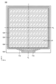
- FIG. 1 is a schematic top view of a radio wave reflector according to one embodiment of the present invention
- FIG. 1 is a schematic top view of a radio wave reflecting element according to one embodiment of the present invention
- FIG. 1 is a schematic end view of a radio wave reflecting element according to one embodiment of the present invention
- FIG. 1 is a schematic end view of a radio wave reflecting element according to one embodiment of the present invention
- FIG. 1 is a schematic end view of a radio wave reflecting element according to one embodiment of the present invention
- FIG. 4 is a schematic end view showing a method of manufacturing a radio wave reflecting element according to one embodiment of the present invention
- FIG. 4 is a schematic end view showing a method of manufacturing a radio wave reflecting element according to one embodiment of the present invention
- FIG. 4 is a schematic end view showing a method of manufacturing a radio wave reflecting element according to one embodiment of the present invention
- FIG. 2 is a schematic diagram showing characteristics of a radio wave reflector according to one embodiment of the present invention
- FIG. 2 is a schematic diagram showing characteristics of a radio wave reflector according to one embodiment of the present invention
- 1 is a schematic top view of a radio wave reflecting element according to one embodiment of the present invention
- FIG. 1 is a schematic top view of a radio wave reflecting element according to one embodiment of the present invention
- FIG. 1 is a schematic top view of a radio wave reflecting element according to one embodiment of the present invention
- FIG. 1 is a schematic top view of a radio wave reflecting element according to one embodiment of the present invention
- FIG. 1 is a schematic top view of a radio wave reflecting element according to one embodiment of the present invention
- FIG. 1 is a schematic top view of a radio wave reflecting element according to one embodiment of the present invention
- FIG. 1 is a schematic top view of a radio wave reflecting element according to one embodiment of the present invention
- FIG. 1 is a schematic top view of a radio wave reflecting element according to one embodiment
- FIG. 1 is a schematic end view of a radio wave reflecting element according to one embodiment of the present invention
- FIG. 1 is a schematic end view of a radio wave reflecting element according to one embodiment of the present invention
- FIG. 1 is a schematic top view of a radio wave reflector according to one embodiment of the present invention
- 1 is a schematic end view of a radio wave reflecting element according to one embodiment of the present invention
- drawings may schematically represent the width, thickness, shape, etc. of each part compared to the actual embodiment, but this is only an example and does not limit the interpretation of the present invention. not something to do.
- elements having the same functions as those described with respect to the previous drawings may be denoted by the same reference numerals, and redundant description may be omitted.
- the term “above” means that the structure is in contact with the structure unless otherwise specified. , includes both the case of arranging another structure directly above and the case of arranging another structure above a certain structure via another structure.
- a structure is exposed from another structure means that a part of a structure is not covered by another structure, and the other structure The portion that is not covered by the body also includes a mode covered by another structure.
- a radio wave reflector 100 which is one embodiment of the present invention, will be described.
- the radio wave reflector 100 has a function of reflecting the emitted radio wave in an arbitrary direction.
- the frequency of the wavelength that can be reflected is in the range of 400 MHz to 50 GHz, typically radio waves in the 400 MHz to 6.0 GHz band, radio waves in the 2.5 GHz to 4.7 GHz band, radio waves in the 24 GHz to 50 GHz band, and the like.
- FIG. 1 shows a schematic top view of the radio wave reflector 100 .
- the radio wave reflector 100 has a substrate 102 and a counter substrate 104 not shown in FIG.
- 13 radio wave reflecting elements 120 are arranged in the row direction (the x direction in the drawing), and 14 radio wave reflecting elements 120 are arranged in the column direction (the y direction perpendicular to the x direction in the drawing). are arrayed.
- the number of radio wave reflecting elements 120 is not restricted and can be determined arbitrarily. Also, the number of rows and the number of columns are arbitrary and may be the same or different.
- a surface formed by arranging a plurality of radio wave reflecting elements 120, that is, a single surface (reflecting surface) containing all radio wave reflecting elements 120 at the same time may be square, rectangular, or circular.
- the reflective surface has one or more axes of symmetry passing through the reflective surface.
- the substrate 102 and the opposing substrate 104 are fixed to each other by a sealing material 106 containing resin such as epoxy resin or acrylic resin.
- a liquid crystal layer 140 which will be described later, is sealed in a space formed by the substrate 102, the counter substrate 104, and the sealing material .
- a drive circuit 110 for generating a potential (control potential) for controlling the radio wave reflecting element 120 is provided on the substrate 102, and the control potential is applied to a first electrode 122 (described later) of the radio wave reflecting element 120.
- Wiring 112 for supply is connected to the drive circuit 110 and the plurality of radio wave reflecting elements 120 .
- the drive circuit 110 may be formed of a metal film, an insulating film, or a semiconductor film provided on the substrate 102, or may be an IC chip having an integrated circuit provided on a semiconductor substrate.
- FIG. 2 shows a schematic top view of one radio wave reflecting element 120
- FIG. 3 shows a schematic view of an end face along the chain line AA' in FIG. In FIG. 3, along with one radio wave reflecting element 120-1, a portion of the radio wave reflecting element 120-2 adjacent to the radio wave reflecting element 120-1 and the encapsulant 106 are also shown.
- the substrate 102 and the counter substrate 104 are provided to give physical strength to the radio wave reflector 100 and to provide a surface for arranging the radio wave reflection element 120 and the drive circuit 110 for driving it.
- Substrate 102 and/or counter substrate 104 may be flexible.
- the substrate 102 and the counter substrate 104 can contain inorganic insulators such as glass and quartz, semiconductors such as silicon, polymers such as polyimide, polycarbonate, and polyester, and metals such as aluminum, copper, and stainless steel.
- the surface on which the radio wave reflecting element 120 is provided that is, the surface of the substrate 102 facing the opposing substrate 104 and the surface of the opposing substrate 104 facing the substrate 102 may contain silicon oxide or nitride.
- At least one of the substrate 102 and the counter substrate 104 is configured to transmit at least part of ultraviolet rays or part of visible light.
- the substrate 102 and/or the counter substrate 104 are configured to transmit at least a portion of light in the wavelength range of 300 nm to 800 nm, preferably light in the wavelength range of 300 nm to 400 nm.
- each radio wave reflecting element 120 includes a first electrode (also called a patch electrode) 122 sandwiched between the substrate 102 and the counter substrate 104, a second electrode 124, and a second electrode 124.
- a first alignment film 130, a second alignment film 132, a third alignment film 134, a fourth alignment film 136, and a liquid crystal layer 140 are provided as a basic configuration. For ease of viewing, only the first electrode 122, the second alignment film 132, and the second electrode 124 are shown in FIG.
- the first electrode 122 is provided on the substrate 102 .
- the first electrode 122 may be formed on the substrate 102 via an undercoat 128 consisting of one or more films containing inorganic compounds such as silicon oxide and silicon nitride.
- the first electrodes 122 of the radio wave reflecting elements 120 adjacent in the column direction or row direction are electrically connected to each other for conduction. Therefore, for example, the first electrodes 122 of the plurality of radio wave reflecting elements 120 arranged in one row are electrically connected to each other and have the same potential, but in this case, these first electrodes 122 are arranged in another row.
- first electrode 122 of the radio wave reflecting element 120 It is not electrically connected to the first electrode 122 of the radio wave reflecting element 120 which is connected to the ground. Similarly, when the first electrodes 122 of the plurality of radio wave reflecting elements 120 arranged in one row are electrically connected to each other and have the same potential, these first electrodes 122 are connected to the radio waves arranged in other rows. It does not conduct with the first electrode 122 of the reflective element 120 .
- the first electrode 122 is made of, for example, a metal such as copper, aluminum, tungsten, molybdenum, or titanium, an alloy containing at least one of these metals, or indium-tin oxide (ITO) or indium-zinc oxide (IZO). ) and other conductive oxides.
- the first electrode 122 may have a single-layer structure or a laminated structure in which layers with different compositions are stacked.
- the first electrode 122 may be formed by a sputtering method, a chemical vapor deposition (CVD) method, or the like.
- the first electrode 122 does not occupy the entire surface occupied by one radio wave reflecting element 120 on the substrate 102, but partially occupies it. Therefore, in the examples shown in FIGS. 2 and 3, a portion including the center of the surface occupied by each radio wave reflecting element 120 is occupied by the first electrode 122, and the other region is in the second orientation described later.
- a film 132 and a third alignment film 134 are arranged.
- the first alignment film 130 is provided to control the orientation of liquid crystal molecules forming the liquid crystal layer 140 provided thereon.
- a first alignment film 130 is disposed on the first electrode 122 and covers the first electrode 122 .
- the first alignment film 130 is continuously provided over the plurality of radio wave reflecting elements 120 . In other words, it is shared by all the radio wave reflecting elements 120 without being separated between adjacent radio wave reflecting elements 120 .
- the first alignment film 130 contains polymers such as polyimide and polyester.
- the first alignment film 130 is formed using a wet film formation method such as an inkjet method, a spin coat method, a printing method, or a dip coating method, and its surface is rubbed.
- a second alignment film 132 is also provided to control the alignment of liquid crystal molecules.
- the second alignment film 132 contains a polymer having a composition different from that of the first alignment film 130 .
- the second alignment film 132 includes a linear or crosslinked polymer having side chains exhibiting liquid crystallinity.
- the basic skeleton of the polymer that constitutes the second alignment film 132 includes poly(meth)acrylate, polyoxyethylene, polyester, polysilane, polyamide, polyurethane, polysiloxane, and the like.
- the side chains contain rigid substituents (mesogens) and further contain spacers connecting the rigid substituents and the main chain.
- the side chains may further comprise terminal groups attached to rigid substituents that are not attached to the main chain.
- rigid substituents include aromatic substituents such as biphenyl groups in which a plurality of aromatic rings are directly bonded, aromatic imino groups, azobenzene groups, aromatic ester groups, stilbene groups, diarylacetylenes, and the like.
- Spacers include alkyl groups, alkoxy groups, ester groups, and the like.
- Terminal groups include alkyl groups, alkoxy groups, alkyl ester groups, cyano groups, and the like. A method for manufacturing the second alignment film 132 will be described later.
- the second alignment film 132 is provided so as not to overlap the first electrode 122 . That is, the second alignment film 132 does not overlap or substantially does not overlap the first electrode 122 in the direction perpendicular to the top surface of the substrate 102 . Therefore, the first alignment film 130 is exposed from the second alignment film 132 and is in direct contact with the liquid crystal layer 140 in the region overlapping the first electrode. On the other hand, the second alignment film 132 is in direct contact with the liquid crystal layer 140 in regions other than the above regions, and is sandwiched between the first alignment film 130 and the liquid crystal layer 140 . In other words, the second alignment film 132 has multiple openings and each opening overlaps the first electrode 122 .
- the second alignment film 132 may be continuous across adjacent radio wave reflecting elements 120 (FIG. 3). That is, the second alignment film 132 may be shared by multiple radio wave reflecting elements 120 .
- the second alignment film 132 is configured such that the long axis of the liquid crystal molecules overlapping the second alignment film 132 is inclined from the upper surface of the substrate 102, and the angle of inclination (tilt angle) is the same as that of the first alignment film. It is configured to be larger than that of the area in direct contact with 130 (ie, the area overlapping the first electrode 122).
- the liquid crystal layer 140 contains liquid crystal molecules.
- the structure of liquid crystal molecules is not limited. Therefore, the liquid crystal molecules may be nematic liquid crystals, smectic liquid crystals, cholesteric liquid crystals, or chiral smectic liquid crystals.
- the liquid crystal layer 140 is in direct contact with the second alignment film 132 , and is in direct contact with the first alignment film 130 in the region overlapping the first electrode 122 .
- the thickness of the liquid crystal layer 140 is, for example, 20 ⁇ m or more and 100 ⁇ m or less, or 30 ⁇ m or more and 50 ⁇ m or less. Therefore, the height of the encapsulant 106 is also selected from this range.
- spacers may be provided in the liquid crystal layer 140 in order to maintain this thickness over the entire radio wave reflector 100 . Note that when the thickness of the liquid crystal layer 140 described above is adopted in a liquid crystal display device, the high responsiveness necessary for displaying moving images cannot be obtained, and it is extremely difficult to exhibit the function of the liquid crystal display device. becomes.
- the third alignment film 134 is provided to control the alignment of liquid crystal molecules, and has the same composition and structure as the second alignment film 132. .
- the third alignment film 134 overlaps the second alignment film 132 and does not overlap or substantially does not overlap the first electrode 122 .
- the third alignment film 134 is in direct contact with the liquid crystal layer 140 in areas other than the area overlapping the first electrode 122 .
- the third alignment film 134 also has an opening overlapping the first electrode 122 . Therefore, the second alignment film 132 and the third alignment film 134 have openings that overlap each other.
- the shapes of the openings of the second alignment film 132 and the third alignment film 134 may be the same or different.
- the third alignment film 134 may also be continuous across adjacent radio wave reflecting elements 120 (FIG. 3). That is, the third alignment film 134 may also be shared by the plurality of radio wave reflecting elements 120 .
- the tilt angle of the liquid crystal molecules positioned on the third alignment film 134 is the region directly contacting the first alignment film 130 and the fourth alignment film (ie , the region overlapping the first electrode 122).
- the fourth alignment film 136 has the same function as the first alignment film 130 and aligns the liquid crystal molecules.
- the fourth alignment film 136 has the same composition and structure as the first alignment film 130, and also has the same rubbing direction.
- the fourth alignment film 136 overlaps the first electrode 122 and the second electrode 124 and is continuously provided over the plurality of radio wave reflecting elements 120 . Further, the fourth alignment film 136 does not overlap the second alignment film 132 or the fourth alignment film 136 in the region overlapping the first electrode 122 .
- the fourth alignment film 136 is exposed from the third alignment film 134 and directly contacts the liquid crystal layer 140 in the region overlapping the first electrode.
- the third alignment film 134 is in direct contact with the liquid crystal layer 140 in regions other than this region, and is sandwiched between the fourth alignment film 136 and the liquid crystal layer 140 .
- the second electrode 124 is provided on the counter substrate 104 (under the counter substrate 104 in FIG. 3).
- the second electrode 124 may be formed on the substrate 102 through an overcoat 138 comprising one or more films comprising inorganic compounds such as silicon oxide or silicon nitride.
- the second electrode 124 is provided over all the radio wave reflecting elements 120 . That is, the second electrode 124 is shared by all radio wave reflecting elements 120 .
- a constant potential is supplied to the second electrode 124 from an external circuit via wiring (not shown).
- the second electrode 124 is also made of metal such as copper, aluminum, tungsten, molybdenum, titanium, an alloy containing at least one of these metals, or indium-tin oxide (ITO). Conductive oxides such as indium-zinc oxide (IZO) may also be included.
- the second electrode 124 may also have a single-layer structure, or may have a laminated structure in which layers with different compositions are laminated.
- the second electrode 124 may also be formed by applying a sputtering method, a chemical vapor deposition (CVD) method, or the like.
- FIGS. 4A and 4B show three radio wave reflecting elements 120 in series.
- a first electrode 122 and a first alignment film 130 are sequentially formed on a substrate 102 in the same manner as in a known liquid crystal display device.
- a second electrode 124 and a fourth alignment film 136 are formed on the opposing substrate 104 .
- the first alignment film 130 and the fourth alignment film 136 are subjected to rubbing treatment.
- the first alignment film 130 and the fourth alignment film 136 are arranged between the substrate 102 and the counter substrate 104 so that the rubbing directions of the first alignment film 130 and the fourth alignment film 136 are the same.
- the substrate 102 and the counter substrate 104 are arranged so as to be sandwiched between them, and the substrate 102 and the counter substrate 104 are bonded together using the sealing material 106 .
- the liquid crystal layer 140 is injected into the space surrounded by the substrate 102 , the opposing substrate 104 and the sealing material 106 .
- an uncured or partially cured sealant 106 is provided on either the substrate 102 or the counter substrate 104 , and the liquid crystal layer 140 is dropped onto a region surrounded by the sealant 106 .
- the other of the substrate 102 and the counter substrate 104 may be placed on the sealing material 106 and the sealing material 106 may be cured.
- the liquid crystal layer 140 contains a reactive mesogen (indicated by a circle in the figure) and a photoinitiator (not shown).
- a reactive mesogen is a molecule having a polymerizable substituent and a rigid substituent in the same molecule via a spacer. give. Reactive mesogens may be oligomeric.
- the photoinitiator is a molecule that absorbs ultraviolet light or visible light to generate cationic species or radicals, and known photoinitiators can be used.
- the irradiated light includes light of wavelengths that are absorbed by the photoinitiator.
- the first electrode 122 does not transmit the irradiation light
- the irradiation light is partially blocked by the first electrode 122, and the irradiation light is selectively absorbed by the photoinitiator in the region where the first electrode 122 is not provided. and the polymerization and/or cross-linking of the reactive mesogen proceeds.
- the second alignment film 132 and the third alignment film 134 are selectively formed on the first alignment film 130 and the fourth alignment film 136, respectively, in the region where the first electrode 122 is not provided. (See FIG. 3).
- light irradiation may be performed through a photomask 114 having a light transmitting portion 114b and a light shielding portion 114a (FIG. 4B).
- the photomask 114 is configured such that the light-transmitting portion 114 b overlaps with the first electrode 122 and the light-shielding portion 114 a does not overlap with the first electrode 122 .
- the second electrode 124 transmits irradiation light
- light irradiation may be performed from the second electrode 124 side through the photomask 114 .
- the first alignment film 130 and the fourth alignment film 136 are rubbed. Therefore, the rigid substituents of the reactive mesogen before polymerization or cross-linking contained in the liquid crystal layer 140 are oriented in a certain direction between the first alignment film 130 and the fourth alignment film 136, and this state is maintained. Polymerization or cross-linking can be allowed to proceed by light irradiation in this state. Therefore, in the vicinity of the interface between the second alignment film 132 and the liquid crystal layer 140 and in the vicinity of the interface between the third alignment film 134 and the liquid crystal layer 140, the polymer generated by cross-linking the reactive mesogen expands the liquid crystal molecules. It can be fixed at a tilt angle (pretilt angle).
- the second alignment film 132 and the third alignment film 134 have a higher ability to tilt liquid crystal molecules than the first alignment film 130 and the fourth alignment film 136 .
- the pretilt angle of the liquid crystal molecules in the absence of an electric field is larger than in the other regions.
- the region sandwiched between the second alignment film 132 and the third alignment film 134 is defined as a high pretilt region
- the first A region in direct contact with the alignment film 130 and the second alignment film 132 that is, a region in which the first electrode 122 occupies the radio wave reflecting element 120 and overlaps with the first electrode 122
- a low pretilt region In the embodiment of the present invention, by selectively polymerizing or cross-linking reactive mesogens in each radio wave reflecting element 120, a high pretilt area and a low pretilt area can be separately created in each radio wave reflecting element 120.
- FIGS. 5A and 5B show three radio wave reflecting elements 120 in series.
- each radio wave reflecting element 120 has a high pretilt area and a low pretilt area.
- the rubbing directions of the first alignment film 130 and the fourth alignment film 136 are the same, so the liquid crystal molecules tend to assume splay alignment in the absence of an electric field.
- a potential difference is applied between the first electrode 122 and the second electrode 124 by appropriately changing the control potential, an electric field is generated in the liquid crystal layer 140, and the liquid crystal molecules rotate and transition from the splay alignment to the bend alignment. do. Therefore, by appropriately adjusting the control potential, the permittivity of the liquid crystal layer 140 can be greatly changed in each radio wave reflecting element 120 .
- each radio wave reflecting element 120 has a high pretilt region.
- the contribution of the second alignment film 132 and the third alignment film 134 allows the liquid crystal molecules to be greatly tilted even in the absence of an electric field, and to assume a strongly bend-aligned state. That is, the average tilt angle is large.
- the first electrode 122 does not exist in the high pretilt region, even if a potential difference is applied between the first electrode 122 and the second electrode 124, no electric field is generated in this high pretilt region. Therefore, this bend orientation does not depend on the magnitude of the electric field. In other words, strong bend orientation stably exists in the high pretilt region.
- the low pretilt region is affected by the orientation of the adjacent high pretilt region and can have a relatively high tilt angle even in the absence of an electric field, as shown in FIG. 5A.
- the average tilt angle of the liquid crystal molecules in the low pretilt region is smaller than that in the high pretilt region, but larger than that in the absence of the high pretilt region. That is, in the low pretilt region, the liquid crystal molecules can take a pseudo-bend alignment even in the absence of an electric field.
- the liquid crystal molecules in the low pretilt region having pseudo bend orientation can respond at high speed and transition to the bend orientation (FIG. 5B). Therefore, a high response speed can be obtained.
- the radio wave reflecting plate 100 including the radio wave reflecting element 120 having the above configuration can function as a radio wave reflecting plate capable of switching the reflection direction of radio waves.
- a situation is assumed in which the radio wave reflector 100 is irradiated with radio waves (wavy lines in the drawing).
- a constant potential is applied to the second electrode 124 .
- a separate control potential is applied from the drive circuit 110 for each column or row. Accordingly, the tilt angles of the liquid crystal molecules included in the liquid crystal layer 140 change for each column or row, and as a result, the dielectric constant of the liquid crystal layer 140 changes for each column or row.
- the dielectric constant changes, the amount of change in the phase shift of the reflected wave also changes, so the phase shift of the reflected wave from the radio wave reflector 100 also shifts for each column or row.
- the traveling direction of the radio wave changes. That is, it becomes possible to reflect radio waves at a reflection angle different from the incident angle of the radio waves.
- the incident angle of radio waves is 0°, but the reflection angle is larger than 0°.
- the amount of change in the phase changes, so the angle of reflection can be arbitrarily controlled.
- the uniaxial radio wave reflecting plate having the reflection axis Ay extending in the column direction The radio wave reflector 100 can be made to function.
- radio waves are reflected as a uniaxial radio wave reflector having a reflection axis Ax extending in the row direction.
- the plate 100 can be made functional.
- each radio wave reflecting element 120 is provided with a high pretilt area and a low pretilt area.
- the high pretilt region does not contribute to dielectric constant control of the liquid crystal layer 140
- the liquid crystal layer 140 in the low pretilt region that contributes to dielectric constant control can be quasi-bend aligned in the absence of an electric field. can be bend-aligned with a high response speed.
- Such a mechanism allows the radio wave reflector 100 to function as a radio wave reflector having a high response speed.
- the planar shape of the first electrode 122 (the shape of the closed surface of the substrate 102), and a shape without openings as shown in FIG. 2 may be used.
- a shape having one or more openings (or slits) is also possible. That is, in each radio wave reflecting element 120, the first electrode 122 may have a ring shape.
- the shape of the opening may be polygonal, including squares and rectangles, and the outline of the opening may be composed of curved lines.
- the aperture may be circular (FIG. 7C) or elliptical (FIG. 7D).
- the first electrode 122 has an axis of symmetry A s parallel to the reflection axis of the radio wave reflector 100 .
- the shape of the second electrode 124 is also arbitrary, and may be a shape that does not have an opening and is continuous over the entire reflecting surface (see FIGS. 1 and 3).
- the second electrode 124 may have an aperture that overlaps at least a portion of the aperture of the first electrode 122 .
- the opening of the second electrode 124 may overlap the entire opening of the first electrode 122 .
- the shape of the opening of the second electrode 124 may be set arbitrarily, and may be polygonal including squares and rectangles, or may be a circle, an ellipse, or the like whose outline is partly or entirely curved.
- the shape of the opening of the second electrode 124 may be the same as that of the opening of the first electrode 122, or may be different.
- the second alignment film 132 and the third alignment film 134 are arranged so as not to overlap the first electrode 122 and the second electrode 124 .
- each radio wave reflecting element 120 has a high pretilt region overlapping the second alignment film 132 and the third alignment film 134, and the second alignment film 132 and the third alignment film 134 are separated from each other.
- a low pretilt region is formed that does not overlap and overlaps the first electrode 122 . Therefore, the high pretilt region allows the liquid crystal in the low pretilt region to take a pseudo-bend alignment. Due to this, the liquid crystal layer 140 in the low pretilt region responds to the electric field at high speed and transitions to the bend alignment, so that each radio wave reflecting element 120 can produce a large dielectric anisotropy change.
- FIG. 10 A schematic top view of the radio wave reflecting plate 150 is shown in FIG. 10, and an example of an equivalent circuit of each radio wave reflecting element 120 is shown in FIG.
- One of the differences between the radio wave reflector 150 and the radio wave reflector 150 is that in the radio wave reflector 150, the first electrodes 122 of the plurality of radio wave reflectors 120 are not electrically connected to each other and are controlled independently.
- two drive circuits a gate line drive circuit 152 and a signal line drive circuit 154 ) for controlling the plurality of radio wave reflection elements 120 are provided on the substrate 102 .
- a plurality of gate wirings 156 extend in the row direction from the gate line driving circuit 152 , and the gate line driving circuit 152 supplies gate signals to the plurality of radio wave reflecting elements 120 connected to each gate wiring 156 .
- the signal line drive circuit 154 is connected to a plurality of signal lines 158 extending in the column direction via the wiring 112, and supplies a control potential to the plurality of radio wave reflecting elements 120 connected to each signal line 158.
- the gate line driver circuit 152 and the signal line driver circuit 154 may be formed of a metal film, an insulating film, or a semiconductor film provided over the substrate 102, or an IC chip having an integrated circuit provided over the semiconductor substrate. may be formed by placing on the substrate 102 .
- the number of gate line driving circuits 152 is not limited, and for example, a pair of gate line driving circuits 152 may be provided so as to sandwich a reflecting surface.
- each radio wave reflecting element 120 has at least one transistor 160, a gate wiring 156 is connected to its gate electrode, and a signal line is connected to one terminal (first terminal). 158 are connected. The other terminal (second terminal) of transistor 160 is connected to first electrode 122 for controlling liquid crystal layer 140 .
- each wave reflecting element 120 may have a capacitive element 180 between the gate wiring and the second terminal of the transistor.
- the radio wave reflecting element 120 may further include a transistor and a capacitive element.
- Transistor 160 is provided directly on substrate 102 or through undercoat 128 .
- a transistor 160 illustrated in FIG. 12 is a so-called bottom-gate transistor, and includes a gate electrode 162, a gate insulating film 164 over the gate electrode 162, a semiconductor film 166 over the gate insulating film 164, and a first semiconductor film 166 over the semiconductor film 166. It has a terminal 168 and a second terminal 170 .
- the transistor 160 may be a top-gate transistor or a dual-gate transistor having gate electrodes 162 above and below a semiconductor film 166, respectively.
- Semiconductor film 166 may include a Group 14 element such as silicon, or may be an oxide semiconductor such as indium-gallium oxide or indium-gallium-zinc oxide.
- the first terminal 168 and the second terminal 170 are provided with a first interlayer insulating film 172 made of one or more films containing silicon oxide or silicon nitride.
- a conductive connection pad 174 is electrically connected to the second terminal 170 through the provided opening.
- a planarizing film 178 for absorbing irregularities caused by the transistor 160 and the like to provide a flat upper surface is provided directly or via a second interlayer insulating film 176 on the connection pad 174 .
- the planarizing film 178 and the second interlayer insulating film 176 are provided with openings exposing the connection pads 174, and the first electrodes 122 formed on the planarizing film 178 are electrically connected to the connection pads 174 through the openings.
- a third interlayer insulating film 182 may be formed between the planarizing film 178 and the first electrode 122 .
- the second electrode 124 is provided over the plurality of radio wave reflecting elements 120 and is supplied with a constant potential.
- the transistor 160 operates by a gate signal supplied to the gate wiring 156, and a control potential is supplied from the signal line 158 to the first electrode 122 through the transistor 160 when the transistor 160 is on.
- an electric field based on the potential difference between the control potential and the constant potential applied to the second electrode 124 is applied to the liquid crystal layer 140 . Therefore, by sequentially selecting the radio wave reflecting elements 120 for each row using a plurality of gate wirings 156 and sequentially supplying a control potential from a plurality of signal lines to the selected radio wave reflecting elements 120, a plurality of radio wave reflections can be achieved.
- the radio wave reflector 150 is a biaxial radio wave reflector having two reflection axes Ay and Ax extending in the column direction and the column direction (the y direction and the x direction in FIG. 10, respectively). can function as
- the radio wave reflecting plate 150 is also provided with the radio wave reflecting elements 120 described in the first embodiment, and each radio wave reflecting element 120 is provided with a high pretilt area and a low pretilt area. Therefore, the liquid crystal layer 140 in the low pretilt region, which contributes to permittivity control, can be quasi-bend-aligned in the absence of an electric field, and the liquid crystal layer 140 in the low pretilt region can be bend-aligned with a high response speed. With such a mechanism, the radio wave reflector 150 can function as a radio wave reflector having a high response speed.
- Radio wave reflector 102: substrate, 104: counter substrate, 106: sealing material
- 110 drive circuit
- 112 wiring
- 114 photomask
- 114a light shielding part
- 114b translucent part
- 120 radio wave reflection Element
- 120-1 radio wave reflecting element
- 120-2 radio wave reflecting element
- 122 first electrode
- 124 second electrode
- 128 undercoat
- 130 first alignment film
- 132 second Alignment film
- 140 Liquid crystal layer
- 158 signal line
- 160 transistor
- 162 gate electrode
- 164 gate insulating film
- 166 semiconductor film
- 168 first terminal
- 170 second terminal
- 172 first interlayer insulation film
- 174 connection pad
- 176 second interlayer insulating film
- 178 planarizing film
- 180 capacitive element
Landscapes
- Physics & Mathematics (AREA)
- Nonlinear Science (AREA)
- Electromagnetism (AREA)
- Chemical & Material Sciences (AREA)
- Crystallography & Structural Chemistry (AREA)
- General Physics & Mathematics (AREA)
- Optics & Photonics (AREA)
- Spectroscopy & Molecular Physics (AREA)
- Mathematical Physics (AREA)
- Liquid Crystal (AREA)
Abstract
Description
本発明の実施形態の一つは、電波反射素子、および電波反射素子を備える電波反射板に関する。 One embodiment of the present invention relates to a radio wave reflecting element and a radio wave reflecting plate provided with the radio wave reflecting element.
液晶分子は誘電率異方性を有しているため、液晶分子を含む液晶層に印加される電場を調整して液晶分子の配向を制御することで、液晶層の誘電率を制御することができる。例えば特許文献1や2では、液晶層に印加される電場を調整することで特性制御可能なメタサーフェスが開示されている。
Since liquid crystal molecules have dielectric anisotropy, the dielectric constant of the liquid crystal layer can be controlled by adjusting the electric field applied to the liquid crystal layer containing the liquid crystal molecules to control the orientation of the liquid crystal molecules. can. For example,
本発明の実施形態の一つは、新しい構造を有する電波反射素子を備える電波反射板を提供することを課題の一つとする。あるいは、本発明の実施形態の一つは、高速で反射方向の切替が可能な電波反射素子を備える電波反射板を提供することを課題の一つとする。 An object of one of the embodiments of the present invention is to provide a radio wave reflector having a radio wave reflecting element with a new structure. Another object of one of the embodiments of the present invention is to provide a radio wave reflecting plate having a radio wave reflecting element capable of switching the reflection direction at high speed.
本発明の実施形態の一つは、電波反射素子である。この電波反射素子は、第1の電極、第1の配向膜、第2の配向膜、液晶層、第3の配向膜、第4の配向膜、および第2の電極を備える。第1の配向膜は第1の電極上に位置する。第2の配向膜は第1の配向膜上に位置し、第1の配向膜と接する。液晶層は、第1の配向膜と第2の配向膜の上に位置し、液晶分子を含む。第3の配向膜は液晶層上に位置する。第4の配向膜は液晶層と第3の配向膜の上に位置し、液晶層と第3の配向膜に接する。第2の電極は第4の配向膜上に位置する。第1の電極と重なる第1の領域において、第1の配向膜と第4の配向膜は、それぞれ第2の配向膜と第3の配向膜から露出する。 One of the embodiments of the present invention is a radio wave reflecting element. This radio wave reflecting element includes a first electrode, a first alignment film, a second alignment film, a liquid crystal layer, a third alignment film, a fourth alignment film, and a second electrode. A first alignment film is located on the first electrode. The second alignment film is positioned on the first alignment film and is in contact with the first alignment film. The liquid crystal layer overlies the first alignment film and the second alignment film and contains liquid crystal molecules. A third alignment film is located on the liquid crystal layer. The fourth alignment film is positioned on the liquid crystal layer and the third alignment film and is in contact with the liquid crystal layer and the third alignment film. A second electrode is located on the fourth alignment film. In the first region overlapping with the first electrode, the first alignment film and the fourth alignment film are exposed from the second alignment film and the third alignment film, respectively.
本発明の実施形態の一つは、電波反射板である。この電波反射板は、マトリクス状に配置された複数の電波反射素子を備える。複数の電波反射素子の各々は、第1の電極、第1の配向膜、第2の配向膜、液晶層、第3の配向膜、第4の配向膜、および第2の電極を備える。第1の配向膜は第1の電極上に位置する。第2の配向膜は第1の配向膜上に位置し、第1の配向膜と接する。液晶層は、第1の配向膜と第2の配向膜の上に位置し、液晶分子を含む。第3の配向膜は液晶層上に位置する。第4の配向膜は液晶層と第3の配向膜の上に位置し、液晶層と第3の配向膜に接する。第2の電極は第4の配向膜上に位置する。第1の電極と重なる第1の領域において、第1の配向膜と第4の配向膜は、それぞれ第2の配向膜と第3の配向膜から露出する。 One of the embodiments of the present invention is a radio wave reflector. This radio wave reflector includes a plurality of radio wave reflection elements arranged in a matrix. Each of the plurality of radio wave reflecting elements includes a first electrode, a first alignment film, a second alignment film, a liquid crystal layer, a third alignment film, a fourth alignment film, and a second electrode. A first alignment film is located on the first electrode. The second alignment film is positioned on the first alignment film and is in contact with the first alignment film. The liquid crystal layer overlies the first alignment film and the second alignment film and contains liquid crystal molecules. A third alignment film is located on the liquid crystal layer. The fourth alignment film is positioned on the liquid crystal layer and the third alignment film and is in contact with the liquid crystal layer and the third alignment film. A second electrode is located on the fourth alignment film. In the first region overlapping with the first electrode, the first alignment film and the fourth alignment film are exposed from the second alignment film and the third alignment film, respectively.
以下、本発明の各実施形態について、図面などを参照しつつ説明する。ただし、本発明は、その要旨を逸脱しない範囲において様々な態様で実施することができ、以下に例示する実施形態の記載内容に限定して解釈されるものではない。 Hereinafter, each embodiment of the present invention will be described with reference to the drawings. However, the present invention can be implemented in various aspects without departing from the gist thereof, and should not be construed as being limited to the description of the embodiments illustrated below.
図面は、説明をより明確にするため、実際の態様に比べ、各部の幅、厚さ、形状などについて模式的に表される場合があるが、あくまで一例であって、本発明の解釈を限定するものではない。本明細書と各図において、既出の図に関して説明したものと同様の機能を備えた要素には、同一の符号を付して、重複する説明を省略することがある。 In order to make the description clearer, the drawings may schematically represent the width, thickness, shape, etc. of each part compared to the actual embodiment, but this is only an example and does not limit the interpretation of the present invention. not something to do. In this specification and each drawing, elements having the same functions as those described with respect to the previous drawings may be denoted by the same reference numerals, and redundant description may be omitted.
本明細書および請求項において、ある構造体の上に他の構造体を配置する態様を表現するにあたり、単に「上に」と表記する場合、特に断りの無い限りは、ある構造体に接するように、直上に他の構造体を配置する場合と、ある構造体の上方に、さらに別の構造体を介して他の構造体を配置する場合との両方を含むものとする。 In this specification and claims, when expressing a mode in which another structure is arranged on top of another structure, the term “above” means that the structure is in contact with the structure unless otherwise specified. , includes both the case of arranging another structure directly above and the case of arranging another structure above a certain structure via another structure.
本明細書および請求項において、「ある構造体が他の構造体から露出する」という表現は、ある構造体の一部が他の構造体によって覆われていない態様を意味し、この他の構造体によって覆われていない部分は、さらに別の構造体によって覆われる態様も含む。 In this specification and claims, the expression "a structure is exposed from another structure" means that a part of a structure is not covered by another structure, and the other structure The portion that is not covered by the body also includes a mode covered by another structure.
(第1実施形態)
本実施形態では、本発明の実施形態の一つである電波反射板100について説明する。電波反射板100は、照射された電波を任意の方向に反射させる機能を有している。反射できる波長の周波数は400MHzから50GHzの範囲であり、典型的には400MHzから6.0GHz帯の電波、2.5GHzから4.7GHz帯の電波、24GHzから50GHz帯の電波などである。
(First embodiment)
In this embodiment, a
1.全体構造
図1に電波反射板100の模式的上面図を示す。電波反射板100は、基板102と図1には示されない対向基板104を有しており、基板102と対向基板104の間にマトリクス状に配列された複数の電波反射素子120が配置される。図1に示された例では、行方向(図中、x方向)に13の電波反射素子120が配列し、列方向(図中、x方向と直交するy方向)に14の電波反射素子120が配列されている。電波反射素子120の数に制約はなく、任意に決定できる。また、行の数と列の数も任意であり、互いに同一でも異なっていてもよい。複数の電波反射素子120が配列することで形成される面、すなわち、全ての電波反射素子120を同時に包含する単一の面(反射面)は正方形でもよく、長方形でもよく、あるいは円でもよい。好ましくは、反射面は、反射面を通過する対称軸を一つまたは複数有する。
1. Overall Structure FIG. 1 shows a schematic top view of the
基板102と対向基板104は、エポキシ樹脂やアクリル樹脂などの樹脂を含む封止材106によって互いに固定される。基板102、対向基板104、および封止材106によって形成される空間に後述する液晶層140が封止される。基板102上には、電波反射素子120を制御するための電位(制御電位)を生成するための駆動回路110が設けられるとともに、制御電位を電波反射素子120の第1の電極122(後述)に供給するための配線112が駆動回路110と複数の電波反射素子120に接続される。駆動回路110は基板102上に設けられる金属膜や絶縁膜、半導体膜によって形成されてもよく、あるいは半導体基板上に設けられた集積回路を有するICチップでもよい。
The
1-1.基板
図2に一つの電波反射素子120の上面模式図を、図3に図1の鎖線A-A´に沿った端面の模式図を示す。図3では、一つの電波反射素子120-1とともに当該電波反射素子120-1に隣接する電波反射素子120-2の一部と封止材106も示されている。
1-1. 2. Substrate FIG. 2 shows a schematic top view of one radio
基板102と対向基板104は、電波反射板100に物理的強度を付与するとともに、電波反射素子120やそれを駆動するための駆動回路110を配置するための面を提供するために設けられる。基板102および/または対向基板104は、可撓性を有してもよい。基板102と対向基板104は、ガラスや石英などの無機絶縁体、ケイ素などの半導体、ポリイミドやポリカルボナート、ポリエステルなどの高分子、アルミニウムや銅、ステンレスなどの金属を含むことができる。金属などの導電性材料が含まれる場合には、電波反射素子120が設けられる面、すなわち、基板102の対向基板104側の面と対向基板104の基板102側の面には、酸化ケイ素や窒化ケイ素などの絶縁体を含む膜を設けることが好ましい。なお、基板102と対向基板104の少なくとも一方は、少なくとも紫外線の一部または可視光の一部を透過するように構成される。例えば、基板102および/または対向基板104は、300nm以上800nm以下の波長範囲の光の少なくとも一部、好ましくは300nm以上400nm以下の波長範囲の光を透過するように構成される。
The
1-2.電波反射素子
図2と図3に示すように、各電波反射素子120は、基板102と対向基板104の間に挟まれる第1の電極(パッチ電極とも呼ばれる)122、第2の電極124、第1の配向膜130、第2の配向膜132、第3の配向膜134、第4の配向膜136、および液晶層140を基本的な構成として備える。なお、見やすさを考慮し、図2では、第1の電極122,第2の配向膜132、および第2の電極124のみが示されている。
1-2. Radio Wave Reflecting Element As shown in FIGS. 2 and 3, each radio
(1)第1の電極
第1の電極122は、基板102上に設けられる。任意の構成として、酸化ケイ素や窒化ケイ素などの無機化合物を含む一つまたは複数の膜で構成されるアンダーコート128を介して第1の電極122が基板102上に形成されてもよい。図2に示すように、電波反射板100においては、列方向または行方向に隣接する電波反射素子120の第1の電極122は、互いに電気的に接続されて導通する。したがって、例えば一つの列に配置される複数の電波反射素子120の第1の電極122は互いに導通されて等電位となるが、この場合、これらの第1の電極122は、他の列に配置される電波反射素子120の第1の電極122とは導通しない。同様に、一つの行に配置される複数の電波反射素子120の第1の電極122が互いに導通されて等電位となる場合、これらの第1の電極122は、他の行に配置される電波反射素子120の第1の電極122とは導通しない。
(1) First Electrode The
第1の電極122は、例えば銅やアルミニウム、タングステン、モリブデン、チタンなどの金属、これらの金属のうち少なくとも一つを含む合金、あるいはインジウム-スズ酸化物(ITO)やインジウム-亜鉛酸化物(IZO)などの導電性酸化物を含む。第1の電極122は単層構造を有してもよく、異なる組成の層が積層された積層構造を有してもよい。第1の電極122は、スパッタリング法や化学気相成長(CVD)法などを適用して形成すればよい。
The
ここで、第1の電極122は、一つの電波反射素子120が基板102上で占める面の全体を占有せず、一部を占有する。したがって、図2や図3で示された例では、各電波反射素子120が占有する面の中心を含む一部が第1の電極122によって占められ、他の領域には後述する第2の配向膜132や第3の配向膜134が配置される。
Here, the
(2)第1の配向膜
第1の配向膜130は、その上に設けられる液晶層140を構成する液晶分子の配向を制御するために設けられる。第1の配向膜130は第1の電極122上に配置され、第1の電極122を覆う。第1の配向膜130は、複数の電波反射素子120に亘って連続的に設けられる。換言すると、隣接する電波反射素子120間で分断されず、全ての電波反射素子120によって共有される。第1の配向膜130は、ポリイミドやポリエステルなどの高分子を含む。第1の配向膜130は、インクジェット法やスピンコート法、印刷法、ディップコーティング法などの湿式成膜法を利用することで形成され、その表面はラビング処理される。
(2) First Alignment Film The
(3)第2の配向膜
第2の配向膜132も液晶分子の配向を制御するために設けられる。第2の配向膜132は、第1の配向膜130とは異なる組成を有する高分子を含む。具体的には、第2の配向膜132は、液晶性を示す側鎖を有する直鎖または架橋された高分子を含む。このような高分子の構造に制約はない。例えば第2の配向膜132を構成する高分子の基本骨格としては、ポリ(メタ)アクリレート、ポリオキシエチレン、ポリエステル、ポリシラン、ポリアミド、ポリウレタン、ポリシロキサンなどが挙げられる。側鎖は剛直性置換基(メソゲン)を含み、さらに剛直性置換基と主鎖を連結するスペーサを含む。側鎖はさらに、主鎖とは結合せずに剛直性置換基に結合された末端基を含んでもよい。剛直性置換基としては、ビフェニル基などの複数の芳香環が直接結合した芳香族置換基、芳香族イミノ基、アゾベンゼン基、芳香族エステル基、スチルベン基、ジアリールアセチレン、などが挙げられる。スペーサとしては、アルキル基、アルコキシ基、エステル基などが挙げられる。末端基としては、アルキル基、アルコキシ基、アルキルエステル基、シアノ基などが挙げられる。第2の配向膜132の作製方法は後述する。
(3) Second Alignment Film A
第2の配向膜132は、第1の電極122と重ならないように設けられる。すなわち、基板102の上面に垂直な方向において、第2の配向膜132は第1の電極122と重ならない、または実質的に重ならない。このため、第1の電極と重なる領域において、第1の配向膜130は第2の配向膜132から露出し、液晶層140と直接接する。一方、第2の配向膜132は、上記領域以外の領域において液晶層140と直接接し、第1の配向膜130と液晶層140に挟まれる。言い換えると、第2の配向膜132は複数の開口を有し、各開口は第1の電極122と重なる。第2の配向膜132は、隣接する電波反射素子120に亘って連続してもよい(図3)。すなわち、第2の配向膜132は、複数の電波反射素子120によって共有されてもよい。
The
第2の配向膜132は、第2の配向膜132と重なる液晶分子の長軸が基板102の上面から傾くように構成され、かつ、その傾きの角度(チルト角)が、第1の配向膜130と直接接する領域(すなわち、第1の電極122と重なる領域)のそれよりもより大きくなるように構成される。
The
(4)液晶層
液晶層140は液晶分子を含む。液晶分子の構造は限定されない。したがって、液晶分子はネマチック液晶でもよく、あるいはスメクチック液晶、コレステリック液晶、キラルスメチック液晶でもよい。
(4) Liquid Crystal Layer The
液晶層140は第2の配向膜132と直接接し、第1の電極122と重なる領域において第1の配向膜130と直接接する。液晶層140の厚さは、例えば20μm以上100μm以下、または30μm以上50μm以下である。したがって、封止材106の高さもこの範囲から選択される。図示しないが、この厚さを電波反射板100の全体に亘って維持するため、スペーサを液晶層140内に設けてもよい。なお、上述した液晶層140の厚さを液晶表示装置において採用した場合、動画を表示するために必要な高い応答性を得ることができず、液晶表示装置としての機能を発現することが著しく困難となる。
The
(5)第3の配向膜
第2の配向膜132と同様、第3の配向膜134も液晶分子の配向を制御するために設けられ、第2の配向膜132と同一の組成、構造を有する。第3の配向膜134は第2の配向膜132と重なり、第1の電極122と重ならない、または実質的に重ならない。換言すると、第3の配向膜134は、第1の電極122と重なる領域以外の領域で液晶層140と直接接する。第2の配向膜132と同様、第3の配向膜134も第1の電極122と重なる開口を有する。したがって、第2の配向膜132と第3の配向膜134は、互いに重なる開口を備える。第2の配向膜132と第3の配向膜134の開口の形状は同一でも異なってもよい。第3の配向膜134も隣接する電波反射素子120に亘って連続してもよい(図3)。すなわち、第3の配向膜134も複数の電波反射素子120によって共有されてもよい。
(5) Third Alignment Film Similar to the
上述したように、第3の配向膜134は第2の配向膜132と同一の構成を有するため、液晶分子のチルトへの寄与も同様である。したがって、第3の配向膜134上に位置する液晶分子、すなわち、第3の配向膜134と重なる液晶分子のチルト角は、第1の配向膜130や第4の配向膜と直接接する領域(すなわち、第1の電極122と重なる領域)のそれよりも大きい。
As described above, since the
(6)第4の配向膜
第4の配向膜136は第1の配向膜130と同様の機能を有し、液晶分子を配向させる。第4の配向膜136は第1の配向膜130と同様の組成、構造を有し、ラビング方向も同じである。第4の配向膜136は、第1の電極122と第2の電極124と重なり、複数の電波反射素子120に亘って連続的に設けられる。また、第4の配向膜136は第1の電極122と重なる領域においては第2の配向膜132や第4の配向膜136と重ならない。換言すると、第1の電極と重なる領域において、第4の配向膜136は第3の配向膜134から露出し、液晶層140と直接接する。一方、第3の配向膜134は、この領域以外の領域において液晶層140と直接接し、第4の配向膜136と液晶層140に挟まれる。
(6) Fourth Alignment Film The
(7)第2の電極
第2の電極124は、対向基板104上(図3においては対向基板104の下)に設けられる。任意の構成として、酸化ケイ素や窒化ケイ素などの無機化合物を含む一つまたは複数の膜で構成されるオーバーコート138を介して第2の電極124が基板102上に形成されてもよい。図2や図3に示す例では、第2の電極124は全ての電波反射素子120に亘って設けられる。すなわち、第2の電極124は、全ての電波反射素子120によって共有される。第2の電極124には、図示しない配線を介し、外部回路から一定電位が供給される。
(7) Second Electrode The
第1の電極122と同様、第2の電極124も例えば銅やアルミニウム、タングステン、モリブデン、チタンなどの金属、これらの金属のうち少なくとも一つを含む合金、あるいはインジウム-スズ酸化物(ITO)やインジウム-亜鉛酸化物(IZO)などの導電性酸化物を含んでもよい。第2の電極124も単層構造を有してもよく、異なる組成の層が積層された積層構造を有してもよい。第2の電極124もスパッタリング法や化学気相成長(CVD)法などを適用して形成すればよい。
Similar to the
2.電波反射板の作製方法
図4Aと図4Bに示す端面図を用いて電波反射板100の作製方法について説明する。これらの図では、連続する三つの電波反射素子120が示されている。公知の液晶表示装置と同様、基板102上に第1の電極122と第1の配向膜130を順次形成する。一方、対向基板104上に第2の電極124と第4の配向膜136を形成する。第1の配向膜130と第4の配向膜136には、ラビング処理が施される。
2. Method for Producing Radio Wave Reflector A method for producing the
その後、第1の配向膜130と第4の配向膜136のラビング方向が同一になるように、かつ、第1の配向膜130と第4の配向膜136が基板102と対向基板104の間に挟まれるように基板102と対向基板104を配置し、封止材106を用いて基板102と対向基板104を貼り合わせる。その後、基板102、対向基板104、および封止材106で囲まれた空間に対して液晶層140を注入する。あるいは、基板102と対向基板104のいずれか一方の上に硬化前または部分的に硬化した封止材106を設け、封止材106に囲まれた領域に液晶層140を滴下する。その後、基板102と対向基板104の他方を封止材106上に配置し、封止材106を硬化してもよい。
After that, the
この時、図4Aに示されるように、液晶層140には反応性メソゲン(図中、〇印で示される)と光開始剤(図示しない)が含まれる。反応性メソゲンは、スペーサを介して重合性置換基と剛直性置換基を同一分子内に有する分子であり、重合することによって側鎖に剛直性置換基を有する直鎖または架橋された高分子を与える。反応性メソゲンはオリゴマーでもよい。光開始剤は、紫外光または可視光を吸収してカチオン種またはラジカルを生成する分子であり、公知の光開始剤を用いることができる。
At this time, as shown in FIG. 4A, the
液晶層140を挟む基板102と対向基板104を貼り合わせた状態で第1の電極122側から光を照射する(図4Aにおける矢印参照)。照射される光(照射光)は、光開始剤が吸収する波長の光を含む。第1の電極122が照射光を透過しない場合、第1の電極122によって照射光が一部遮蔽され、第1の電極122が設けられていない領域において選択的に照射光が光開始剤によって吸収され、反応性メソゲンの重合および/または架橋が進行する。その結果、第1の電極122が設けられていない領域において、第1の配向膜130と第4の配向膜136上にそれぞれ選択的に第2の配向膜132と第3の配向膜134が形成される(図3参照)。
With the
第1の電極122が照射光を透過する場合には、透光部114bと遮光部114aを有するフォトマスク114を介して光照射を行ってもよい(図4B)。フォトマスク114は、透光部114bが第1の電極122と重なり、遮光部114aが第1の電極122と重ならないように構成される。なお、第2の電極124が照射光を透過する場合には、フォトマスク114を介して第2の電極124側から光照射を行ってもよい。
When the
上述したように、第1の配向膜130と第4の配向膜136にはラビング処理が施されている。このため、液晶層140に含まれる重合または架橋前の反応性メソゲンの剛直性置換基が第1の配向膜130と第4の配向膜136の間で一定の方向に配向し、この状態を維持したまま光照射によって重合または架橋を進行させることができる。このため、第2の配向膜132と液晶層140との界面付近、および第3の配向膜134と液晶層140との界面付近において、反応性メソゲンを架橋して生じたポリマーが液晶分子を大きなチルト角(プレチルト角)で固定することができる。これに起因し、第2の配向膜132と第3の配向膜134は、第1の配向膜130や第4の配向膜136と比較して液晶分子をチルトさせる能力が高い。その結果、第2の配向膜132と第3の配向膜134に挟まれる領域では、それ以外の領域と比較し、電界非存在下における液晶分子のプレチルト角が大きくなる。以下、液晶層140のうち、第2の配向膜132と第3の配向膜134に挟まれる領域を高プレチルト領域、第2の配向膜132と第3の配向膜134に挟まれず、第1の配向膜130と第2の配向膜132と直接接する領域(すなわち、第1の電極122が電波反射素子120内で占める領域であり、第1の電極122と重なる領域)を低プレチルト領域と呼ぶ。本発明の実施形態では、各電波反射素子120内で反応性メソゲンを選択的に重合または架橋させることで、各電波反射素子120内において高プレチルト領域と低プレチルト領域を作り分けることができる。
As described above, the
3.動作
図5Aと図5Bに示す模式的端面図を用いて電波反射板100の動作について説明する。これらの図では、連続する三つの電波反射素子120が示されている。
3. Operation The operation of the
上述したように、各電波反射素子120は、高プレチルト領域と低プレチルト領域を有する。低プレチルト領域では、第1の配向膜130と第4の配向膜136のラビング方向は同一であるため、電界の非存在下では、液晶分子はスプレイ配向を取る傾向にある。一方、制御電位を適宜変化させて第1の電極122と第2の電極124の間に電位差を与えると、液晶層140に電界が発生し、液晶分子が回転してスプレイ配向からベンド配向へ遷移する。このため、制御電位を適宜調整することで、各電波反射素子120において液晶層140の誘電率を大きく変化させることができる。
As described above, each radio
通常スプレイ配向からベンド配向への遷移は遅いため、誘電率変化に必要な時間(応答時間)が長くなる。しかしながら、各電波反射素子120は高プレチルト領域を有している。高プレチルト領域においては、第2の配向膜132と第3の配向膜134の寄与により、電界非存在下においても液晶分子は大きくチルトし、強くベンド配向した状態を取ることができる。すなわち、平均チルト角が大きい。また、高プレチルト領域には第1の電極122が存在しないため、第1の電極122と第2の電極124の間に電位差を与えても、この高プレチルト領域には電界が発生しない。このため、このベンド配向は電界の大きさに依存しない。換言すると、高プレチルト領域では、強いベンド配向が安定的に存在する。
Since the transition from the splay orientation to the bend orientation is usually slow, the time required for the dielectric constant change (response time) increases. However, each radio
その結果、低プレチルト領域は隣接する高プレチルト領域の配向の影響を受け、図5Aに示すように、電界非存在下においても比較的高いチルト角を有することができる。具体的には、電界非存在下においては、低プレチルト領域の液晶分子の平均チルト角は、高プレチルト領域のそれよりは小さいものの、高プレチルト領域が存在しないときと比較すると大きい。すなわち、低プレチルト領域では、電界非存在下でも液晶分子は疑似的なベンド配向を取ることができる。この状態で電界を液晶層140に与えると、疑似的なベンド配向を取る低プレチルト領域の液晶分子は高速で応答してベンド配向へ遷移することができる(図5B)。このため、大きな応答速度を得ることができる。
As a result, the low pretilt region is affected by the orientation of the adjacent high pretilt region and can have a relatively high tilt angle even in the absence of an electric field, as shown in FIG. 5A. Specifically, in the absence of an electric field, the average tilt angle of the liquid crystal molecules in the low pretilt region is smaller than that in the high pretilt region, but larger than that in the absence of the high pretilt region. That is, in the low pretilt region, the liquid crystal molecules can take a pseudo-bend alignment even in the absence of an electric field. When an electric field is applied to the
したがって、上記構成を有する電波反射素子120を備える電波反射板100は、電波の反射方向を切り替えることが可能な電波反射板として機能することができる。例えば図6Aに示すように電波反射板100に電波(図中、波線)が照射される状況を想定する。この時、第2の電極124に一定の電位を与える。一方、第1の電極122に対しては、駆動回路110から列または行ごとに個別の制御電位を与える。これにより、液晶層140に含まれる液晶分子のチルト角が列または行ごとに変化し、その結果、列または行ごとに液晶層140の誘電率が変化する。誘電率が変化すると、反波の移相の変化量が変化するため、電波反射板100からの反射波の移相も列または行ごとにシフトする。その結果、電波の進行方向が変化する。すなわち、電波の入射角とは異なる反射角で電波を反射することが可能となる。例えば図6A、図6Bで示された例では、電波の入射角は0°であるが、反射角は0°よりも大きい。
Therefore, the radio
第1の電極122に印加する制御電位を適宜制御することで位相の変化量が変化するため、反射角は任意に制御可能である。具体的には、列方向(図1におけるy方向)に隣接する電波反射素子120の第1の電極122が等電位である場合、列方向に延伸する反射軸Ayを有する一軸電波反射板として電波反射板100を機能させることができる。逆に、行方向(図1におけるx方向)に隣接する電波反射素子120の第1の電極122が等電位である場合、行方向に延伸する反射軸Axを有する一軸電波反射板として電波反射板100を機能させることができる。
By appropriately controlling the control potential applied to the
以上述べたように、本発明の実施形態に係る電波反射板100では、各電波反射素子120に高プレチルト領域と低プレチルト領域が設けられる。高プレチルト領域は液晶層140の誘電率制御には寄与しないものの、誘電率制御に寄与する低プレチルト領域の液晶層140を電界非存在下において疑似的にベンド配向させることができるため、低プレチルト領域の液晶層を大きな応答速度でベンド配向させることができる。このような機構により、電波反射板100が大きな応答速度を有する電波反射板として機能することができる。
As described above, in the radio
4.変形例
第1の電極122の平面の形状(基板102の閉口な面における形状)に制約はなく、図2に示すように開口を持たない形状でもよく、図7Aや図7Bに示すように、一つまたは複数の開口(またはスリット)を有する形状でもよい。すなわち、各電波反射素子120において、第1の電極122はリング形状を有していてもよい。開口の形状は正方形や長方形を含む多角形でもよく、開口の輪郭は曲線で構成されてもよい。具体的には、開口は円(図7C)や楕円(図7D)でもよい。好ましくは、第1の電極122は、電波反射板100の反射軸と平行な対称軸Asを有する。
4. Modifications There are no restrictions on the planar shape of the first electrode 122 (the shape of the closed surface of the substrate 102), and a shape without openings as shown in FIG. 2 may be used. A shape having one or more openings (or slits) is also possible. That is, in each radio
第2の電極124の形状も任意であり、開口を持たず、反射面の全体に亘って連続する形状でもよい(図1、図3参照)。
The shape of the
あるいは、四つの電波反射素子120の上面模式図である図8、および図8の鎖線B-B´、C-C´に沿った端面の模式図(図9A、図9B)に示すように、第1の電極122が開口を有する場合(図7Aから図7D参照)、第2の電極124は、第1の電極122の開口の少なくとも一部と重なる開口を有してもよい。第2の電極124の開口は、第1の電極122の開口の全体と重なってもよい。第1の電極122と同様、第2の電極124の開口の形状も任意に設定すればよく、正方形や長方形を含む多角形でもよく、あるいは円や楕円など、輪郭の一部または全てが曲線で構成されていてもよい。第2の電極124の開口の形状は、第1の電極122の開口と同一でもよく、異なってもよい。第2の配向膜132と第3の配向膜134は、第1の電極122と第2の電極124と重ならないように配置される。
Alternatively, as shown in FIG. 8, which is a schematic top view of the four radio
上述した変形例においても、各電波反射素子120には、第2の配向膜132と第3の配向膜134と重なる高プレチルト領域とともに、第2の配向膜132と第3の配向膜134とは重ならず、第1の電極122と重なる低プレチルト領域が形成される。したがって、高プレチルト領域によって低プレチルト領域の液晶は疑似的ベンド配向を取ることができる。これに起因し、低プレチルト領域の液晶層140は電界に対して高速に応答してベンド配向へ遷移し、各電波反射素子120に大きな誘電率異方性変化を作り出すことができる。
Also in the above-described modification, each radio
(第2実施形態)
本実施形態では、第1実施形態で述べた電波反射板100とは構造が異なる電波反射板150について説明する。第1実施形態で述べた構成と同一または類似する構成については、説明を割愛することがある。
(Second embodiment)
In this embodiment, a
電波反射板150の模式的上面図を図10に、各電波反射素子120の等価回路の一例を図11に示す。電波反射板150が電波反射板150と異なる点の一つは、電波反射板150では複数の電波反射素子120の第1の電極122は互いに導通せずに独立して制御されることである。具体的には、基板102上には、複数の電波反射素子120を制御する二つの駆動回路(ゲート線駆動回路152、信号線駆動回路154)が設けられる。ゲート線駆動回路152からは複数のゲート配線156が行方向に延伸し、ゲート線駆動回路152は、各ゲート配線156に接続される複数の電波反射素子120に対してゲート信号を供給する。一方、信号線駆動回路154は、配線112を介して列方向に延伸する複数の信号線158に接続され、各信号線158に接続される複数の電波反射素子120に対して制御電位を供給する。なお、ゲート線駆動回路152と信号線駆動回路154は、基板102上に設けられる金属膜や絶縁膜、半導体膜によって形成されてもよく、あるいは半導体基板上に設けられた集積回路を有するICチップを基板102上に設置することで形成してもよい。また、ゲート線駆動回路152の数にも制約はなく、例えば反射面を挟むように一対のゲート線駆動回路152を設けてもよい。
A schematic top view of the radio
図11の等価回路の一例に示すように、各電波反射素子120は少なくとも一つのトランジスタ160を有し、そのゲート電極にゲート配線156が接続され、一つの端子(第1の端子)に信号線158が接続される。トランジスタ160の他方の端子(第2の端子)は、液晶層140を制御するための第1の電極122と接続される。任意の構成として、各電波反射素子120はゲート配線とトランジスタの第2の端子の間に容量素子180を有してもよい。また、図示しないが、電波反射素子120はさらにトランジスタや容量素子を有してもよい。
As shown in an example of the equivalent circuit in FIG. 11, each radio
図12に一つの電波反射素子120の端面模式図を示す。トランジスタ160は基板102上に直接、またはアンダーコート128を介して設けられる。図12に例示されるトランジスタ160は所謂ボトムゲート型トランジスタであり、ゲート電極162、ゲート電極162上のゲート絶縁膜164、ゲート絶縁膜164上の半導体膜166、および半導体膜166上の第1の端子168と第2の端子170を有する。トランジスタ160の構成に制約はなく、トップゲート型トランジスタでもよく、あるいは半導体膜166の上下にそれぞれゲート電極162を有するデュアルゲート型トランジスタでもよい。また、第1の端子168と半導体膜166、および第2の端子170と半導体膜166の上限関係にも制約はない。半導体膜166はケイ素などの14族元素を含んでもよく、あるいはインジウム-ガリウム酸化物やインジウム-ガリウム-亜鉛酸化物のような酸化物半導体でもよい。
A schematic end view of one radio
第1の端子168と第2の端子170には、酸化ケイ素や窒化ケイ素を含む膜の一つまたは複数で構成される第1の層間絶縁膜172が設けられ、第1の層間絶縁膜172に設けられる開口を介して導電性を有する接続パッド174が第2の端子170と電気的に接続される。接続パッド174上には、トランジスタ160などに起因する凹凸を吸収して平坦な上面を与えるための平坦化膜178が直接、または第2の層間絶縁膜176を介して設けられる。平坦化膜178と第2の層間絶縁膜176には接続パッド174を露出する開口が設けられ、平坦化膜178上に形成される第1の電極122がこの開口を介して接続パッド174と電気的に接続される。任意の構成として、平坦化膜178と第1の電極122の間に第3の層間絶縁膜182を形成してもよい。
The
電波反射板150においても、第2の電極124は複数の電波反射素子120に亘って設けられ、一定電位が供給される。一方、ゲート配線156に供給されるゲート信号によってトランジスタ160が動作し、トランジスタ160がオンの時に信号線158から制御電位がトランジスタ160を介して第1の電極122に供給される。その結果、制御電位と第2の電極124に印加される定電位との電位差に基づく電界が液晶層140に印加される。したがって、複数のゲート配線156を用いて電波反射素子120を行ごとに順次選択し、選択された電波反射素子120に対して複数の信号線から制御電位を順次供給することで、複数の電波反射素子120に対してそれぞれ独立して任意に設定された制御電位を供給することができる。換言すると、複数の電波反射素子120において、個別に液晶層140の誘電率を制御することができる。このため、電波反射板150は電波反射板100と異なり、列方向と列方向(それぞれ図10におけるy方向とx方向)に延伸する二つの反射軸Ay、Axを有する二軸電波反射板として機能することができる。
In the radio
電波反射板150においても、第1実施形態で述べた電波反射素子120が設けられ、各電波反射素子120には高プレチルト領域と低プレチルト領域が設けられる。このため、誘電率制御に寄与する低プレチルト領域の液晶層140を電界非存在下において疑似的ベンド配向させることができ、低プレチルト領域の液晶層140を大きな応答速度でベンド配向させることができる。このような機構により、電波反射板150は大きな応答速度を有する電波反射板として機能することができる。
The radio
本発明の実施形態として上述した各実施形態は、相互に矛盾しない限りにおいて、適宜組み合わせて実施することができる。また、各実施形態の電波反射素子または電波反射板を基にして、当業者が適宜構成要素の追加、削除もしくは設計変更を行ったもの、または、工程の追加、省略もしくは条件変更を行ったものも、本発明の要旨を備えている限り、本発明の範囲に含まれる。 Each of the embodiments described above as embodiments of the present invention can be implemented in combination as appropriate as long as they do not contradict each other. In addition, based on the radio wave reflecting element or radio wave reflecting plate of each embodiment, those skilled in the art appropriately added, deleted, or changed the design of components, or added, omitted, or changed the conditions of processes. are also included in the scope of the present invention as long as they have the gist of the present invention.
上述した各実施形態の態様によりもたらされる作用効果とは異なる他の作用効果であっても、本明細書の記載から明らかなもの、または、当業者において容易に予測し得るものについては、当然に本発明によりもたらされるものと解される。 Even if there are other effects different from the effects brought about by the aspects of each embodiment described above, those that are obvious from the description of this specification or those that can be easily predicted by those skilled in the art are of course It is understood that it is provided by the present invention.
100:電波反射板、102:基板、104:対向基板、106:封止材、110:駆動回路、112:配線、114:フォトマスク、114a:遮光部、114b:透光部、120:電波反射素子、120-1:電波反射素子、120-2:電波反射素子、122:第1の電極、124:第2の電極、128:アンダーコート、130:第1の配向膜、132:第2の配向膜、134:第3の配向膜、136:第4の配向膜、138:オーバーコート、140:液晶層、150:電波反射板、152:ゲート線駆動回路、154:信号線駆動回路、156:ゲート配線、158:信号線、160:トランジスタ、162:ゲート電極、164:ゲート絶縁膜、166:半導体膜、168:第1の端子、170:第2の端子、172:第1の層間絶縁膜、174:接続パッド、176:第2の層間絶縁膜、178:平坦化膜、180:容量素子
100: radio wave reflector, 102: substrate, 104: counter substrate, 106: sealing material, 110: drive circuit, 112: wiring, 114: photomask, 114a: light shielding part, 114b: translucent part, 120: radio wave reflection Element, 120-1: radio wave reflecting element, 120-2: radio wave reflecting element, 122: first electrode, 124: second electrode, 128: undercoat, 130: first alignment film, 132: second Alignment film 134: Third alignment film 136: Fourth alignment film 138: Overcoat 140: Liquid crystal layer 150: Radio wave reflector 152: Gate line drive circuit 154: Signal line drive circuit 156 : gate wiring, 158: signal line, 160: transistor, 162: gate electrode, 164: gate insulating film, 166: semiconductor film, 168: first terminal, 170: second terminal, 172: first interlayer insulation film, 174: connection pad, 176: second interlayer insulating film, 178: planarizing film, 180: capacitive element
Claims (20)
前記第1の電極上の第1の配向膜、
前記第1の配向膜上に位置し、前記第1の配向膜と接する第2の配向膜、
前記第1の配向膜と前記第2の配向膜の上に位置し、液晶分子を含む液晶層、
前記液晶層上の第3の配向膜、
前記液晶層と前記第3の配向膜の上に位置し、前記液晶層と前記第3の配向膜に接する第4の配向膜、および
前記第4の配向膜上の第2の電極を備え、
前記第1の電極と重なる第1の領域において、前記第1の配向膜と前記第4の配向膜は、それぞれ前記第2の配向膜と前記第3の配向膜から露出する、電波反射素子。 a first electrode;
a first alignment film on the first electrode;
a second alignment film located on the first alignment film and in contact with the first alignment film;
a liquid crystal layer located on the first alignment film and the second alignment film and containing liquid crystal molecules;
a third alignment film on the liquid crystal layer;
a fourth alignment film located on the liquid crystal layer and the third alignment film and in contact with the liquid crystal layer and the third alignment film; and a second electrode on the fourth alignment film,
The radio wave reflecting element, wherein the first alignment film and the fourth alignment film are exposed from the second alignment film and the third alignment film, respectively, in a first region overlapping with the first electrode.
前記第2の配向膜は、前記第1の領域以外の領域において前記第1の配向膜と前記液晶層に挟まれ、
前記第3の配向膜は、前記第1の領域以外の領域において前記第4の配向膜と前記液晶層に挟まれる、請求項1に記載の電波反射素子。 the first alignment film and the fourth alignment film are in direct contact with the liquid crystal layer in the first region;
the second alignment film is sandwiched between the first alignment film and the liquid crystal layer in a region other than the first region;
2. The radio wave reflecting element according to claim 1, wherein said third alignment film is sandwiched between said fourth alignment film and said liquid crystal layer in a region other than said first region.
前記第2の配向膜と前記第3の配向膜は、前記第1の開口と重なる、請求項1に記載の電波反射素子。 the first electrode having a first opening;
2. The radio wave reflecting element according to claim 1, wherein said second alignment film and said third alignment film overlap said first opening.
前記複数の電波反射素子の各々は、
第1の電極、
前記第1の電極上の第1の配向膜、
前記第1の配向膜上に位置し、前記第1の配向膜と接する第2の配向膜、
前記第1の配向膜と前記第2の配向膜の上に位置し、液晶分子を含む液晶層、
前記液晶層上の第3の配向膜、
前記液晶層と前記第3の配向膜の上に位置し、前記液晶層と前記第3の配向膜に接する第4の配向膜、および
前記第4の配向膜上の第2の電極を備え、
前記第1の電極と重なる第1の領域において、前記第1の配向膜と前記第4の配向膜は、それぞれ前記第2の配向膜と前記第3の配向膜から露出する、電波反射板。 Equipped with multiple radio wave reflection elements arranged in a matrix,
Each of the plurality of radio wave reflecting elements,
a first electrode;
a first alignment film on the first electrode;
a second alignment film located on the first alignment film and in contact with the first alignment film;
a liquid crystal layer located on the first alignment film and the second alignment film and containing liquid crystal molecules;
a third alignment film on the liquid crystal layer;
a fourth alignment film located on the liquid crystal layer and the third alignment film and in contact with the liquid crystal layer and the third alignment film; and a second electrode on the fourth alignment film,
The radio wave reflector, wherein in a first region overlapping with the first electrode, the first alignment film and the fourth alignment film are exposed from the second alignment film and the third alignment film, respectively.
前記第2の配向膜は、前記第1の領域以外の領域において前記第1の配向膜と前記液晶層に挟まれ、
前記第3の配向膜は、前記第1の領域以外の領域において前記第4の配向膜と前記液晶層に挟まれる、請求項10に記載の電波反射板。 the first alignment film and the fourth alignment film are in direct contact with the liquid crystal layer in the first region;
the second alignment film is sandwiched between the first alignment film and the liquid crystal layer in a region other than the first region;
11. The radio wave reflector according to claim 10, wherein said third alignment film is sandwiched between said fourth alignment film and said liquid crystal layer in a region other than said first region.
前記第2の配向膜と前記第3の配向膜は、前記第1の開口と重なる、請求項10に記載の電波反射板。 the first electrode having a first opening;
11. The radio wave reflector according to claim 10, wherein said second alignment film and said third alignment film overlap said first opening.
20. The radio wave reflector according to claim 19, wherein said first opening and said second opening have the same shape.
Priority Applications (3)
| Application Number | Priority Date | Filing Date | Title |
|---|---|---|---|
| JP2023552711A JPWO2023058319A1 (en) | 2021-10-07 | 2022-08-08 | |
| CN202280065386.7A CN118020213A (en) | 2021-10-07 | 2022-08-08 | Radio wave reflecting element and radio wave reflecting plate |
| US18/624,181 US20240243485A1 (en) | 2021-10-07 | 2024-04-02 | Intelligent reflecting surface |
Applications Claiming Priority (2)
| Application Number | Priority Date | Filing Date | Title |
|---|---|---|---|
| JP2021-165552 | 2021-10-07 | ||
| JP2021165552 | 2021-10-07 |
Related Child Applications (1)
| Application Number | Title | Priority Date | Filing Date |
|---|---|---|---|
| US18/624,181 Continuation US20240243485A1 (en) | 2021-10-07 | 2024-04-02 | Intelligent reflecting surface |
Publications (1)
| Publication Number | Publication Date |
|---|---|
| WO2023058319A1 true WO2023058319A1 (en) | 2023-04-13 |
Family
ID=85804123
Family Applications (1)
| Application Number | Title | Priority Date | Filing Date |
|---|---|---|---|
| PCT/JP2022/030215 Ceased WO2023058319A1 (en) | 2021-10-07 | 2022-08-08 | Radio wave reflection element and radio wave reflection plate |
Country Status (4)
| Country | Link |
|---|---|
| US (1) | US20240243485A1 (en) |
| JP (1) | JPWO2023058319A1 (en) |
| CN (1) | CN118020213A (en) |
| WO (1) | WO2023058319A1 (en) |
Cited By (4)
| Publication number | Priority date | Publication date | Assignee | Title |
|---|---|---|---|---|
| WO2025033055A1 (en) * | 2023-08-08 | 2025-02-13 | 株式会社ジャパンディスプレイ | Radio wave reflecting device |
| WO2025121083A1 (en) * | 2023-12-07 | 2025-06-12 | 株式会社ジャパンディスプレイ | Radio wave reflection element, radio wave reflection device provided with radio wave reflection element, and antenna |
| WO2025127070A1 (en) * | 2023-12-11 | 2025-06-19 | 京セラ株式会社 | Composite resonator and radio wave control plate |
| WO2025204884A1 (en) * | 2024-03-29 | 2025-10-02 | 京セラ株式会社 | Radio wave control plate |
Citations (3)
| Publication number | Priority date | Publication date | Assignee | Title |
|---|---|---|---|---|
| JP2003529259A (en) * | 2000-03-29 | 2003-09-30 | エイチアールエル ラボラトリーズ,エルエルシー | Electronic tunable reflector |
| JP2007522735A (en) * | 2004-02-10 | 2007-08-09 | テレフオンアクチーボラゲット エル エム エリクソン(パブル) | Adjustable device |
| JP2022025914A (en) * | 2020-07-30 | 2022-02-10 | 株式会社ジャパンディスプレイ | Driving method of phased array antenna and driving method of reflector |
Family Cites Families (4)
| Publication number | Priority date | Publication date | Assignee | Title |
|---|---|---|---|---|
| TWI315423B (en) * | 2005-12-30 | 2009-10-01 | Ind Tech Res Inst | Substrate structures, liquid crystal display devices and method of fabricating liquid crystal display devices |
| TW200801733A (en) * | 2006-06-23 | 2008-01-01 | Ind Tech Res Inst | Liquid crystal display devices and fabrication methods thereof |
| TW200825577A (en) * | 2006-12-14 | 2008-06-16 | Ind Tech Res Inst | Optically compensated bend mode liquid crystal display devices and fabrication methods thereof |
| KR20150137148A (en) * | 2014-05-28 | 2015-12-09 | 삼성디스플레이 주식회사 | Liquid crystal display devices and methods of manufacturing the same |
-
2022
- 2022-08-08 WO PCT/JP2022/030215 patent/WO2023058319A1/en not_active Ceased
- 2022-08-08 JP JP2023552711A patent/JPWO2023058319A1/ja active Pending
- 2022-08-08 CN CN202280065386.7A patent/CN118020213A/en active Pending
-
2024
- 2024-04-02 US US18/624,181 patent/US20240243485A1/en active Pending
Patent Citations (3)
| Publication number | Priority date | Publication date | Assignee | Title |
|---|---|---|---|---|
| JP2003529259A (en) * | 2000-03-29 | 2003-09-30 | エイチアールエル ラボラトリーズ,エルエルシー | Electronic tunable reflector |
| JP2007522735A (en) * | 2004-02-10 | 2007-08-09 | テレフオンアクチーボラゲット エル エム エリクソン(パブル) | Adjustable device |
| JP2022025914A (en) * | 2020-07-30 | 2022-02-10 | 株式会社ジャパンディスプレイ | Driving method of phased array antenna and driving method of reflector |
Cited By (4)
| Publication number | Priority date | Publication date | Assignee | Title |
|---|---|---|---|---|
| WO2025033055A1 (en) * | 2023-08-08 | 2025-02-13 | 株式会社ジャパンディスプレイ | Radio wave reflecting device |
| WO2025121083A1 (en) * | 2023-12-07 | 2025-06-12 | 株式会社ジャパンディスプレイ | Radio wave reflection element, radio wave reflection device provided with radio wave reflection element, and antenna |
| WO2025127070A1 (en) * | 2023-12-11 | 2025-06-19 | 京セラ株式会社 | Composite resonator and radio wave control plate |
| WO2025204884A1 (en) * | 2024-03-29 | 2025-10-02 | 京セラ株式会社 | Radio wave control plate |
Also Published As
| Publication number | Publication date |
|---|---|
| JPWO2023058319A1 (en) | 2023-04-13 |
| US20240243485A1 (en) | 2024-07-18 |
| CN118020213A (en) | 2024-05-10 |
Similar Documents
| Publication | Publication Date | Title |
|---|---|---|
| WO2023058319A1 (en) | Radio wave reflection element and radio wave reflection plate | |
| KR102492786B1 (en) | Liquid crystal display apparatus | |
| JP5307467B2 (en) | Display device | |
| US11221521B2 (en) | Display device | |
| KR20130026277A (en) | Alignment layer for display device, liquid crystal display device including the same and method and apparatus for treating the same | |
| JPH11326927A (en) | Liquid crystal display device | |
| KR20090092939A (en) | Display device and method of manufacturing for the same | |
| US20100141859A1 (en) | Display device including uv-absorbing filter | |
| US20240405441A1 (en) | Intelligent reflecting surface | |
| WO2018038209A1 (en) | Scanning antenna and method of manufacturing scanning antenna | |
| JP2004212943A (en) | Structure for reducing light diffraction effect due to cyclic arrangement of electrodes and liquid crystal display device having the structure | |
| US10824020B2 (en) | Polarization independent optical phase modulator | |
| TW594350B (en) | Liquid crystal display device | |
| KR101382480B1 (en) | Liquid crystal display | |
| JP7352480B2 (en) | display device | |
| JP2024078133A (en) | Radio wave reflector | |
| WO2025220602A1 (en) | Radio wave reflection device | |
| US20260018800A1 (en) | Intelligent reflecting surface | |
| WO2025169809A1 (en) | Radio wave reflection device | |
| CN113176683A (en) | Display device | |
| WO2024157610A1 (en) | Radio wave reflection device | |
| WO2025033055A1 (en) | Radio wave reflecting device | |
| US20250372872A1 (en) | Intelligent reflecting surface and method for driving the intelligent reflecting surface | |
| JP4745013B2 (en) | Liquid crystal display | |
| WO2025121083A1 (en) | Radio wave reflection element, radio wave reflection device provided with radio wave reflection element, and antenna |
Legal Events
| Date | Code | Title | Description |
|---|---|---|---|
| 121 | Ep: the epo has been informed by wipo that ep was designated in this application |
Ref document number: 22878190 Country of ref document: EP Kind code of ref document: A1 |
|
| WWE | Wipo information: entry into national phase |
Ref document number: 2023552711 Country of ref document: JP |
|
| WWE | Wipo information: entry into national phase |
Ref document number: 202280065386.7 Country of ref document: CN |
|
| NENP | Non-entry into the national phase |
Ref country code: DE |
|
| 122 | Ep: pct application non-entry in european phase |
Ref document number: 22878190 Country of ref document: EP Kind code of ref document: A1 |