WO2022141312A1 - Photosensitive sensor and manufacturing method therefor, and movable platform - Google Patents
Photosensitive sensor and manufacturing method therefor, and movable platform Download PDFInfo
- Publication number
- WO2022141312A1 WO2022141312A1 PCT/CN2020/141836 CN2020141836W WO2022141312A1 WO 2022141312 A1 WO2022141312 A1 WO 2022141312A1 CN 2020141836 W CN2020141836 W CN 2020141836W WO 2022141312 A1 WO2022141312 A1 WO 2022141312A1
- Authority
- WO
- WIPO (PCT)
- Prior art keywords
- region
- doping
- photosensitive
- light
- photosensitive sensor
- Prior art date
- Legal status (The legal status is an assumption and is not a legal conclusion. Google has not performed a legal analysis and makes no representation as to the accuracy of the status listed.)
- Ceased
Links
Images


Classifications
-
- H—ELECTRICITY
- H10—SEMICONDUCTOR DEVICES; ELECTRIC SOLID-STATE DEVICES NOT OTHERWISE PROVIDED FOR
- H10F—INORGANIC SEMICONDUCTOR DEVICES SENSITIVE TO INFRARED RADIATION, LIGHT, ELECTROMAGNETIC RADIATION OF SHORTER WAVELENGTH OR CORPUSCULAR RADIATION
- H10F77/00—Constructional details of devices covered by this subclass
- H10F77/30—Coatings
- H10F77/306—Coatings for devices having potential barriers
-
- G—PHYSICS
- G01—MEASURING; TESTING
- G01S—RADIO DIRECTION-FINDING; RADIO NAVIGATION; DETERMINING DISTANCE OR VELOCITY BY USE OF RADIO WAVES; LOCATING OR PRESENCE-DETECTING BY USE OF THE REFLECTION OR RERADIATION OF RADIO WAVES; ANALOGOUS ARRANGEMENTS USING OTHER WAVES
- G01S17/00—Systems using the reflection or reradiation of electromagnetic waves other than radio waves, e.g. lidar systems
- G01S17/02—Systems using the reflection of electromagnetic waves other than radio waves
-
- H—ELECTRICITY
- H10—SEMICONDUCTOR DEVICES; ELECTRIC SOLID-STATE DEVICES NOT OTHERWISE PROVIDED FOR
- H10F—INORGANIC SEMICONDUCTOR DEVICES SENSITIVE TO INFRARED RADIATION, LIGHT, ELECTROMAGNETIC RADIATION OF SHORTER WAVELENGTH OR CORPUSCULAR RADIATION
- H10F30/00—Individual radiation-sensitive semiconductor devices in which radiation controls the flow of current through the devices, e.g. photodetectors
- H10F30/20—Individual radiation-sensitive semiconductor devices in which radiation controls the flow of current through the devices, e.g. photodetectors the devices having potential barriers, e.g. phototransistors
- H10F30/21—Individual radiation-sensitive semiconductor devices in which radiation controls the flow of current through the devices, e.g. photodetectors the devices having potential barriers, e.g. phototransistors the devices being sensitive to infrared, visible or ultraviolet radiation
- H10F30/22—Individual radiation-sensitive semiconductor devices in which radiation controls the flow of current through the devices, e.g. photodetectors the devices having potential barriers, e.g. phototransistors the devices being sensitive to infrared, visible or ultraviolet radiation the devices having only one potential barrier, e.g. photodiodes
- H10F30/225—Individual radiation-sensitive semiconductor devices in which radiation controls the flow of current through the devices, e.g. photodetectors the devices having potential barriers, e.g. phototransistors the devices being sensitive to infrared, visible or ultraviolet radiation the devices having only one potential barrier, e.g. photodiodes the potential barrier working in avalanche mode, e.g. avalanche photodiodes
-
- H—ELECTRICITY
- H10—SEMICONDUCTOR DEVICES; ELECTRIC SOLID-STATE DEVICES NOT OTHERWISE PROVIDED FOR
- H10F—INORGANIC SEMICONDUCTOR DEVICES SENSITIVE TO INFRARED RADIATION, LIGHT, ELECTROMAGNETIC RADIATION OF SHORTER WAVELENGTH OR CORPUSCULAR RADIATION
- H10F39/00—Integrated devices, or assemblies of multiple devices, comprising at least one element covered by group H10F30/00, e.g. radiation detectors comprising photodiode arrays
- H10F39/10—Integrated devices
- H10F39/103—Integrated devices the at least one element covered by H10F30/00 having potential barriers, e.g. integrated devices comprising photodiodes or phototransistors
-
- H—ELECTRICITY
- H10—SEMICONDUCTOR DEVICES; ELECTRIC SOLID-STATE DEVICES NOT OTHERWISE PROVIDED FOR
- H10F—INORGANIC SEMICONDUCTOR DEVICES SENSITIVE TO INFRARED RADIATION, LIGHT, ELECTROMAGNETIC RADIATION OF SHORTER WAVELENGTH OR CORPUSCULAR RADIATION
- H10F39/00—Integrated devices, or assemblies of multiple devices, comprising at least one element covered by group H10F30/00, e.g. radiation detectors comprising photodiode arrays
- H10F39/10—Integrated devices
- H10F39/107—Integrated devices having multiple elements covered by H10F30/00 in a repetitive configuration, e.g. radiation detectors comprising photodiode arrays
-
- H—ELECTRICITY
- H10—SEMICONDUCTOR DEVICES; ELECTRIC SOLID-STATE DEVICES NOT OTHERWISE PROVIDED FOR
- H10F—INORGANIC SEMICONDUCTOR DEVICES SENSITIVE TO INFRARED RADIATION, LIGHT, ELECTROMAGNETIC RADIATION OF SHORTER WAVELENGTH OR CORPUSCULAR RADIATION
- H10F39/00—Integrated devices, or assemblies of multiple devices, comprising at least one element covered by group H10F30/00, e.g. radiation detectors comprising photodiode arrays
- H10F39/10—Integrated devices
- H10F39/12—Image sensors
-
- H—ELECTRICITY
- H10—SEMICONDUCTOR DEVICES; ELECTRIC SOLID-STATE DEVICES NOT OTHERWISE PROVIDED FOR
- H10F—INORGANIC SEMICONDUCTOR DEVICES SENSITIVE TO INFRARED RADIATION, LIGHT, ELECTROMAGNETIC RADIATION OF SHORTER WAVELENGTH OR CORPUSCULAR RADIATION
- H10F71/00—Manufacture or treatment of devices covered by this subclass
-
- H—ELECTRICITY
- H10—SEMICONDUCTOR DEVICES; ELECTRIC SOLID-STATE DEVICES NOT OTHERWISE PROVIDED FOR
- H10F—INORGANIC SEMICONDUCTOR DEVICES SENSITIVE TO INFRARED RADIATION, LIGHT, ELECTROMAGNETIC RADIATION OF SHORTER WAVELENGTH OR CORPUSCULAR RADIATION
- H10F77/00—Constructional details of devices covered by this subclass
- H10F77/30—Coatings
Definitions
- the present application relates to the technical field of photosensitive sensors, and in particular, to a photosensitive sensor, a manufacturing method thereof, and a movable platform.
- APD avalanche diodes
- TOF time-of-flight sensors
- Silicon-based APDs are widely used, but due to the properties of silicon itself, its ability to absorb infrared light with longer wavelengths is weak, and a thicker active absorption region is required to have better quantum absorption efficiency (QE). It is difficult to form a thick active absorption region in the usual semiconductor process. Due to the insufficient thickness of the active absorption region, the quantum absorption efficiency is low, generally it is difficult to exceed 15%, and the sensor performance is low, which limits its application.
- the present application provides a photosensitive sensor, a manufacturing method thereof, and a movable platform, which have high quantum absorption efficiency.
- an embodiment of the present application provides a photosensitive sensor, including: one or more avalanche diodes, each of the avalanche diodes includes:
- the active photosensitive area has a first side and a second side opposite to the first side, and the second side is provided with a light incident surface:
- a first light-reflecting structure located close to the first side and opposite to the first doped region and the second doped region, for reflecting light from the active photosensitive region back to the active photosensitive area.
- an embodiment of the present application provides a method for fabricating a photosensitive sensor, the method comprising:
- One or more avalanche diodes are formed on the substrate, the avalanche diodes include an active photosensitive region, the active photosensitive region has a first side and a second side opposite the first side, and the The second side is provided with a light incident surface, and the avalanche diode further includes a first doped region and a second doped region located on the first side;
- a first reflective structure is formed near the first side, the first reflective structure is disposed opposite the first doped region and the second doped region, and is used for reflecting light from the active photosensitive region back to the active photosensitive area.
- an embodiment of the present application provides a movable platform, including:
- processor controls the movement of the moving component according to the output signal of the photosensitive sensor.
- the embodiments of the present application provide a photosensitive sensor, a method for manufacturing the same, and a movable platform.
- a reflective structure in the photosensitive sensor, at least part of the light can be repeatedly passed through the active photosensitive area, increasing the number of light in the active photosensitive area. Therefore, the probability of photons being absorbed can be increased, so that the photosensitive sensor has higher quantum absorption efficiency, and the detection accuracy and detection distance of the photosensitive sensor can be improved.
- FIG. 1 is a schematic structural diagram of a photosensitive sensor provided by an embodiment of the present application.
- FIG. 2 is a schematic diagram of the principle of a photosensitive sensor used for distance measurement in an embodiment
- FIG. 3 is a schematic block diagram of a photosensitive sensor in one embodiment
- FIG. 4 is a schematic structural diagram of a photosensitive sensor in an embodiment
- FIG. 5 is a schematic structural diagram of a photosensitive sensor in another embodiment
- FIG. 6 is a schematic structural diagram of a photosensitive sensor in another embodiment
- FIG. 7 is a schematic structural diagram of a photosensitive sensor in yet another embodiment
- FIG. 8 is a schematic structural diagram of a photosensitive sensor in yet another embodiment
- 9a to 9d are schematic diagrams of non-planar structures
- FIG. 10 is a schematic structural diagram of a photosensitive sensor in yet another embodiment
- FIG. 11 is a schematic flowchart of a manufacturing method of a photosensitive sensor provided by an embodiment of the present application.
- FIG. 12 is a schematic structural diagram of a movable platform provided by an embodiment of the present application.
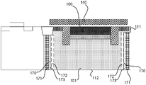
- references numerals 100, avalanche diode; 110, active photosensitive region; 111, first side; 112, second side; 113, fourth doping region; 120, first doping region; 130, second doping region Impurity region; 140, first reflective structure; 150, third doped region; 160, fifth doped region; 170, second reflective structure; 171, deep trench; 172, passivation layer; 173, buffer layer; 101, light incident surface; 102, avalanche breakdown area; 10, readout circuit; 11, shallow trench isolation; 20, peripheral circuit; 30, non-planar structure; 31, blind hole; 32, trench; 700, movable platform; 710, photosensitive sensor; 720, motion component; 701, processor; 702, memory; 703, bus.
- FIG. 1 is a schematic structural diagram of a photosensitive sensor provided by an embodiment of the present application.
- the photosensitive sensor includes an avalanche diode, a time-of-flight sensor, and/or a lidar.
- a photosensitive sensor may be used with the movable platform.
- the movable platform may include at least one of an unmanned aerial vehicle, a gimbal, an unmanned vehicle, an assisted driving vehicle, an unmanned vehicle, and the like.
- the unmanned aerial vehicle may be a rotary-wing drone, such as a quad-rotor drone, a hexa-rotor drone, an octa-rotor drone, or a fixed-wing drone.
- the photosensitive sensor is used for three-dimensional scanning and spatial distance measurement, such as lidar/autopilot/drone barrier/AR (Augmented Reality, augmented reality)/VR (Virtual Reality, virtual reality)/artificial intelligence, etc. Provide input information.
- lidar/autopilot/drone barrier/AR Algmented Reality, augmented reality
- VR Virtual Reality, virtual reality
- artificial intelligence etc.
- the light source is used to actively emit light to illuminate the object, and then the photosensitive sensor is used to receive the light reflected from the object. According to the distance between different positions on the object and the photosensitive sensor, three-dimensional (3D) information of the object can also be obtained.
- the infrared light of a specific wavelength is emitted to illuminate the object, and the avalanche diode 100 is used to receive the infrared light of the specific wavelength reflected back by the object, so as to avoid the interference of natural light in the environment.
- the photosensitive sensor includes one or more avalanche diodes 100 .
- the adjacent avalanche diodes 100 may be isolated by a deep trench isolation (DTI for short) structure or a shallow trench isolation (STI for short) structure to prevent crosstalk between the avalanche diodes 100 .
- DTI deep trench isolation
- STI shallow trench isolation
- the avalanche diode 100 includes an avalanche photodiode (Avalanche Photon Diode, APD).
- Avalanche photodiodes usually add reverse bias to the P-N junction of a photodiode made of silicon or germanium, and the incident light is absorbed by the P-N junction to form a photocurrent. Increasing the reverse bias will generate a photocurrent.
- the phenomenon of "avalanche” that is, the photocurrent surges exponentially), so this kind of diode is called an avalanche photodiode.
- the photosensor further includes a readout circuit 10 .
- the readout circuit 10 includes, for example, an amplifier, such as a transimpedance amplifier, capable of converting the photocurrent into a voltage signal.
- the readout circuit 10 may also include a temperature compensation circuit or the like.
- the photosensitive sensor further includes a peripheral circuit 20, and the peripheral circuit 20 is used to provide a reverse bias voltage to the avalanche diode 100, of course, it is not limited to this, for example, the peripheral circuit 20 can be used to Calculate the distance from the measured object from the time from emission to reflection.
- each avalanche diode 100 includes: an active photosensitive region 110 , a first doped region 120 and a second doped region 130 , and a first reflective structure 140 .
- the active photosensitive region 110 has a first side 111 and a second side 112 opposite to the first side 111 , and the second side 112 is provided with a light incident surface 101 .
- the first doped region 120 and the second doped region 130 are located on the first side 111 .
- the light incident surface 101 may be the surface itself of the second side 112 of the active photosensitive area 110 , but is not limited thereto, for example, may also be the surface of the photosensitive sensor substrate on the side away from the active photosensitive area 110 .
- the substrate may include a substrate and/or an epitaxial layer.
- the doping type of the first doped region 120 and the doping type of the second doped region 130 are different.
- the first doping region 120 is P-type doping
- the second doping region 130 is N-type doping
- the first doping region 120 is N-type doping
- the second doping region 130 is P-type doping .
- the first doped region 120 is used for electrically connecting a first applied voltage
- the second doped region 130 is used for electrically connecting a second applied voltage
- the first applied voltage is different from the second applied voltage.
- a reverse bias voltage can be provided to the avalanche diode 100 through the first doped region 120 and the second doped region 130 .
- metal lines are also provided near the first side 111 , for example, a metal line connected to the first doped region 120 and a metal line connected to the second doped region 130 are provided.
- the side of the photosensitive sensor close to the first side 111 can be referred to as the front of the photosensitive sensor, and the side close to the second side 112 can be referred to as the back of the photosensitive sensor, and the second side 112 of the active photosensitive area 110 is provided with a light incident surface 101 , that is, the photosensitive sensor enters the light through the back, so the photosensitive sensor can be called a back-illuminated photosensitive sensor.
- the photosensitive sensor can be called a back-illuminated photosensitive sensor.
- the first light-reflecting structure 140 is located close to the first side 111 and opposite to the first doped region 120 and the second doped region 130 , and is used to reflect the light from the active photosensitive region 110 back to the active photosensitive region 110 . It can be understood that if the photosensitive sensor does not include the first reflective structure 140, the light from the active photosensitive area 110 will not enter the active photosensitive area 110 after penetrating the active photosensitive area 110.
- the first reflective structure 140 can enable at least part of the light to travel through the active photosensitive area 110 repeatedly, increasing the optical path in the active photosensitive area 110, thereby increasing the probability of photons being absorbed, so that the photosensitive sensor has a higher
- the quantum absorption efficiency can improve the detection accuracy and detection distance of the photosensitive sensor.
- the first light-reflecting structures 140 of different avalanche diodes 100 may be provided separately, or may be provided integrally. It can be determined according to the manufacturing process of the photosensitive sensor.
- the first light-reflecting structures 140 of different avalanche diodes 100 are integrally disposed, the light penetrating the active photosensitive region 110 can be prevented from being transmitted through the space between the first light-reflecting structures 140 of adjacent avalanche diodes 100, so the quantum absorption efficiency higher.
- the surface of the first light-reflecting structure 140 facing the active photosensitive region 110 includes a plane and/or a non-planar curved surface. As shown in FIG. 1 , the surface of the first reflective structure 140 facing the active photosensitive region 110 includes a flat surface. As shown in FIG. 4 , the surface of the first reflective structure 140 facing the active photosensitive region 110 includes a curved surface. Of course, it is not limited to this. For example, the surface of the first light-reflecting structure 140 facing the active photosensitive area 110 may also include an irregular plane, and the light from the active photosensitive area 110 may also be reflected back to the active photosensitive area 110 .
- the curved surface includes at least one of an inner side surface of a cylinder, an inner side surface of an elliptical cylinder, an inner side surface of a sphere, and an inner side surface of an ellipsoid. As shown in FIG. 4 , the curved surface includes the inner side surface of an elliptical cylinder or the inner side surface of an ellipsoid.
- the first light-reflecting structure 140 converges and reflects the light from the active photosensitive area 110 back to the active photosensitive area 110 .
- the surface of the first light-reflecting structure 140 facing the active photosensitive region 110 includes a non-planar curved surface, the convergent reflection of light can be achieved, as shown in FIG. 4 , so that at least part of the light reflected back to the active photosensitive region 110 can be
- the active photosensitive region 110 has a larger optical path and has a higher quantum absorption efficiency.
- the first light-reflecting structure 140 diffusely reflects light from the active photosensitive area 110 back to the active photosensitive area 110 .
- the surface of the first light-reflecting structure 140 facing the active photosensitive region 110 may be a rough surface, such as a rough plane or a rough non-planar curved surface, so that at least part of the light reflected back to the active photosensitive region 110 can be
- the photosensitive area 110 has a larger optical path. For example, when light vertically incident on the active photosensitive area 110 is reflected by the first light-reflecting structure 140 , it is reflected back to the active photosensitive area 110 at a larger angle and has a larger optical path. , with high quantum absorption efficiency.
- the first light-reflecting structure 140 includes a metal layer.
- the material of the metal layer is aluminum, copper, gold, tungsten, or an alloy of at least one of them.
- the first light-reflecting structure 140 includes an oxide layer, such as a silicon dioxide layer.
- the first light-reflecting structure 140 is spaced apart from or integrated with the first doped region 120 and the second doped region 130 .
- the details can be determined according to the manufacturing process of the photosensitive sensor.
- the projection of the first light-reflecting structure 140 on the active photosensitive region 110 at least covers the entire active photosensitive region 110 . Therefore, all the light passing through the first side 111 of the active photosensitive region 110 can be reflected back to the active photosensitive region 110 , with higher quantum absorption efficiency.
- a portion of the first doped region 120 and a third doped region 150 form the avalanche breakdown region 102, and the electric field between the first doped region 120 and the second doped region 130 can
- the carriers generated by driving the active photosensitive region 110 to induce incident light generate an avalanche effect in the avalanche breakdown region 102 , so that the first doped region 120 and the second doped region 130 are turned on.
- the specific structure of the avalanche diode 100 is not limited to this, and FIG. 5 is only for illustration.
- the active photosensitive region 110 includes a fourth doping region 113 , and the doping concentration of the fourth doping region 113 is lower than that of the first doping region 120 and/or the second doping region 113 . Concentration in region 130. Therefore, the active photosensitive region 110 is relatively easy to induce incident light to generate carriers.
- the third doping region 150 is located between the first doping region 120 and the active photosensitive region 110 , and the doping concentration of the third doping region 150 is lower than Doping concentration of the first doping region 120 and/or the second doping region 130 .
- the doping concentration of the third doping region 150 is higher than the doping concentration of the fourth doping region 113 , so that the carriers induced by the active light-sensing region 110 have an avalanche effect in the avalanche breakdown region 102 .
- the avalanche diode 100 further includes a fifth doped region 160 located between the first doped region 120 and the second doped region 130; the fifth doped region 160 is located between the first doped region 120 and the second doped region 130;
- the doping concentration of the impurity region 160 is lower than the doping concentration of the first doping region 120 and/or the second doping region 130 .
- the first doped region 120 and the second doped region 130 are turned on only when the avalanche effect occurs in the avalanche breakdown region 102, thereby improving the accuracy of the photosensitive sensor.
- the first doped region 120 and the third doped region 150 are arranged in layers, and the layers of the stacked first doped region 120 and the third doped region 150 are located in the fifth doped region 160 .
- the second doped region 130 is located on the other side of the fifth doped region 160 .
- the doping types of the first doping region 120 and the fifth doping region 160 are different from the doping types of the second doping region 130 , the third doping region 150 and the fourth doping region 113 ;
- the doping concentration of the first doping region 120 is higher than that of the fifth doping region 160
- the doping concentration of the second doping region 130 is higher than that of the third doping region 150
- the doping concentration of the third doping region 150 is higher than that of the third doping region 150 .
- the doping concentration of 150 is higher than that of the fourth doping region 113 .
- the doping type of the first doping region 120 and the fifth doping region 160 is P-type doping
- the doping type of the second doping region 130 , the third doping region 150 , and the fourth doping region 113 are P-type doping.
- Type is N-type doped.
- the doping type of the first doping region 120 and the fifth doping region 160 is N-type doping
- the doping type of the second doping region 130 , the third doping region 150 and the fourth doping region 113 is P type doping.
- the first doped region 120 is a P+ type heavily doped region
- the second doped region 130 is an N+ heavily doped region
- the third doped region 150 is an N type doped region
- the fourth doped region 113 is an N-lightly doped region.
- the first doping region 120 can be connected to a negative voltage (-10V to -30V)
- the second doping region 130 can be connected to a positive voltage (0v to 10V)
- the fourth doping region 113 is an active region for photon absorption, where light is The region is absorbed to generate electron/hole pairs, and the photogenerated electron-hole pairs enter the third doped region 150 after being accelerated by an electric field, and an avalanche effect occurs when driven by a strong electric field.
- the photosensitive sensor further includes a second reflective structure 170 perpendicular to the surface of the second side 112 , and the second reflective structure 170 is disposed on at least one side of the active photosensitive area 110 ; the second reflective structure 170 It is used to reflect the light from the active photosensitive area 110 back to the active photosensitive area 110 .
- the second light-reflecting structure 170 in the photosensitive sensor, at least part of the light can pass through the active photosensitive area 110 repeatedly, and the optical path in the active photosensitive area 110 is increased, thereby increasing the The probability of photons being absorbed makes the photosensitive sensor have high quantum absorption efficiency, which can improve the detection accuracy and detection distance of the photosensitive sensor.
- the second light-reflecting structure 170 is formed in the deep trench 171 on at least one side of the active photosensitive region 110 . Therefore, the second light-reflecting structure 170 can be provided in the photosensitive sensor through the semiconductor processing technology. For example, after the front surface device of the photosensitive sensor is completed, the deep trench 171 and the second reflective structure 170 are formed by etching the back surface of the photosensitive sensor to the front surface.
- the deep trench 171 extends from the second side 112 toward the first side 111 , so the deep trench 171 may be referred to as a deep back trench 171 (BDTI).
- BDTI deep back trench 171
- the second light-reflecting structure 170 includes HK dielectric material filled in the deep trench 171 .
- the HK dielectric material includes at least one of hafnium oxide, aluminum oxide, and tantalum oxide.
- the HK dielectric material induces a passivation layer 172 on the side of the active photosensitive region 110 close to the second light-reflecting structure 170 , and the passivation layer 172 generates less carriers than the active photosensitive region 170 . Carriers generated by the rest of the region 110 except for the passivation layer 172 .
- the HK dielectric material filled in the deep trench 171 can induce a hole accumulation layer on the surface of silicon close to silicon dioxide, which can passivate the silicon surface and reduce the interference of surface carrier emission on the device. .
- the second light-reflecting structure 170 further includes a buffer layer 173 between the HK dielectric material and the trench walls of the deep trench 171 .
- the buffer layer 173 includes a silicon dioxide buffer layer 173 .
- the silicon dioxide buffer layer 173 is disposed close to the silicon interface of the deep trench 171 .
- the light incident surface 101 is provided with a non-planar structure 30 , and the non-planar structure 30 can change the direction in which light enters the active photosensitive region 110 .
- the non-planar structure 30 can change the direction in which light enters the active photosensitive region 110 .
- the non-planar structure 30 increases the angle of the light entering the active photosensitive region 110, and can be incident on the active photosensitive region 110 obliquely. Since the active photosensitive region 110 is relatively thin, the light is inclined Incident to the active photosensitive region 110 can increase the optical path of light in the active photosensitive region 110 .
- the first light-reflecting structure 140 can also reflect the light to be obliquely incident back to the active photosensitive region 110 , so that the photosensitive sensor has higher quantum absorption efficiency.
- the non-planar structure 30 includes blind holes 31 and/or trenches 32 , which can be formed by an etching process, as shown in FIGS. 9 a to 9 d , where the shaded parts are parts that need to be etched.
- the blind holes 31 may include blind holes 31 with a circular cross section and/or blind holes 31 with a square cross section, but certainly not limited thereto, for example, may include blind holes 31 with a rectangular cross section and the like.
- the grooves 32 include at least one of linear grooves, spiral grooves, and annular grooves.
- the hole wall of the blind hole 31 and/or the groove wall of the groove 32 is perpendicular to the surface of the second side 112 or forms an obtuse angle or an acute angle.
- the width of the notch of the groove 32 is greater than or equal to the width of the groove bottom of the groove 32 .
- a plurality of grooves 32 are arranged in parallel or at least two grooves 32 are intersected.
- the photosensitive sensor includes a first reflective structure 140 , a second reflective structure 170 and a non-planar structure 30 of the light incident surface 101 . More light can be made to repeatedly pass through the active photosensitive area 110, and the optical path in the active photosensitive area 110 can be increased, thereby increasing the probability of photons being absorbed, so that the photosensitive sensor has higher quantum absorption efficiency, The detection accuracy and detection distance of the photosensitive sensor can be improved.
- a shallow trench isolation 11 is provided between the readout circuit 10 and the first doped region 120 , the second doped region 130 , and the avalanche breakdown region 102 to increase the photosensitive Changan device’s reliability.
- the photosensitive sensor provided by the embodiments of the present application, by arranging a reflective structure in the photosensitive sensor, at least part of the light can be repeatedly passed through the active photosensitive area, and the optical path in the active photosensitive area can be increased, thereby increasing the photons being absorbed by the photons.
- the probability of absorption makes the photosensitive sensor have high quantum absorption efficiency, which can improve the detection accuracy and detection distance of the photosensitive sensor.
- FIG. 11 is a schematic flowchart of a manufacturing method of a photosensitive sensor provided by another embodiment of the present application.
- the manufacturing method of the embodiment of the present application includes steps S110 to S130.
- the substrate may include a substrate and/or an epitaxial layer.
- the avalanche diodes including an active photosensitive region, the active photosensitive region having a first side and a second side opposite to the first side, The second side is provided with a light incident surface, and the avalanche diode further includes a first doped region and a second doped region located on the first side.
- thinning processing is performed on the backside of the photosensitive sensor, that is, the substrate, the entire substrate can be removed, or a part of the substrate can be removed, for example, a part of the substrate is still left on the second side of the active photosensitive region.
- the light incident surface may be the surface itself of the second side of the active photosensitive region, but is not limited thereto, for example, it may also be the surface of the photosensitive sensor substrate on the side away from the active photosensitive region.
- the first light-reflecting structure is disposed opposite the first doping region and the second doping region, and is used to convert the light from the active photosensitive region Light is reflected back to the active photosensitive area.
- the surface of the first light-reflecting structure facing the active photosensitive region includes a plane and/or a non-planar curved surface.
- the first light-reflecting structure includes a metal layer.
- the first light-reflecting structure and the first doped region and the second doped region are arranged spaced apart or integrally arranged.
- the projection of the first light-reflecting structure on the substrate at least covers all the active photosensitive regions.
- the manufacturing method further includes: forming a second light-reflecting structure perpendicular to the substrate on a side of the substrate away from the avalanche diode, and the second light-reflecting structure is disposed on the active photosensitive the outer side of the area; the second light-reflecting structure is used for reflecting the light from the active photosensitive area back to the active photosensitive area.
- forming a second light-reflecting structure perpendicular to the substrate on the side of the substrate away from the avalanche diode includes: forming a deep trench on the side of the substrate away from the avalanche diode; The deep trenches are filled with HK dielectric material.
- a buffer layer is formed on the groove wall of the deep trench.
- the manufacturing method further includes: forming a non-planar structure on the light incident surface, and the non-planar structure can change the direction in which light enters the active photosensitive region.
- the non-planar structures include blind holes and/or trenches.
- the manufacturing method of the photosensitive sensor provided by the embodiment of the present application, by arranging a reflective structure in the photosensitive sensor, at least part of the light can be repeatedly passed through the active photosensitive area, and the optical path in the active photosensitive area is increased, so that it can be Increasing the probability of photons being absorbed makes the photosensitive sensor have higher quantum absorption efficiency, which can improve the detection accuracy and detection distance of the photosensitive sensor.
- FIG. 12 is a schematic block diagram of a movable platform 700 provided by an embodiment of the present application.
- the movable platform may include at least one of an unmanned aerial vehicle, a gimbal, an unmanned vehicle, and the like.
- the unmanned aerial vehicle may be a rotary-wing drone, such as a quad-rotor drone, a hexa-rotor drone, an octa-rotor drone, or a fixed-wing drone.
- the movable platform includes the photosensitive sensor 710 and the motion component 720 of the previous embodiment.
- the motion assembly 720 may include one or more propellers, one or more motors corresponding to the one or more propellers, and one or more electronic governors (referred to as ESCs for short).
- Photosensitive sensors 710 include, for example, avalanche diodes, time-of-flight sensors, and/or lidars.
- the photosensitive sensor is used for three-dimensional scanning and spatial distance measurement, such as lidar/autopilot/drone barrier/AR (Augmented Reality, augmented reality)/VR (Virtual Reality, virtual reality)/artificial intelligence, etc. Provide input information.
- lidar/autopilot/drone barrier/AR Algmented Reality, augmented reality
- VR Virtual Reality, virtual reality
- artificial intelligence etc. Provide input information.
- the movable platform 700 includes one or more processors 701 , and the one or more processors 701 work individually or collectively to control the movement of the motion component 720 according to the output signal of the photosensitive sensor 710 .
- the removable platform 700 further includes a memory 702 for storing program instructions.
- the processor 701 and the memory 702 are connected through a bus 703, and the bus 703 is, for example, an I2C (Inter-integrated Circuit) bus.
- I2C Inter-integrated Circuit
- the processor 701 may be a micro-controller unit (Micro-controller Unit, MCU), a central processing unit (Central Processing Unit, CPU) or a digital signal processor (Digital Signal Processor, DSP) or the like.
- MCU Micro-controller Unit
- CPU Central Processing Unit
- DSP Digital Signal Processor
- the memory 702 may be a Flash chip, a read-only memory (ROM, Read-Only Memory) magnetic disk, an optical disk, a U disk, a mobile hard disk, and the like.
- ROM Read-Only Memory
- the memory 702 may be a Flash chip, a read-only memory (ROM, Read-Only Memory) magnetic disk, an optical disk, a U disk, a mobile hard disk, and the like.
- the one or more processors 701 are configured to call program instructions stored in the memory 702 , and when executing the program instructions, control the motion component 720 to move according to the output signal of the photosensitive sensor 710 .
Landscapes
- Physics & Mathematics (AREA)
- Electromagnetism (AREA)
- Engineering & Computer Science (AREA)
- Computer Networks & Wireless Communication (AREA)
- General Physics & Mathematics (AREA)
- Radar, Positioning & Navigation (AREA)
- Remote Sensing (AREA)
- Light Receiving Elements (AREA)
- Optical Radar Systems And Details Thereof (AREA)
Abstract
Description
本申请涉及感光传感器技术领域,尤其涉及一种感光传感器及其制作方法、可移动平台。The present application relates to the technical field of photosensitive sensors, and in particular, to a photosensitive sensor, a manufacturing method thereof, and a movable platform.
利用雪崩二极管(APD)的传感器,如飞行时间传感器(TOF)广泛用于消费电子、安防监控、工业自动化、人工智能、物联网等领域,用于空间距离数据信息的采集和整理,为后续处理和应用提供信息源。Sensors using avalanche diodes (APD), such as time-of-flight sensors (TOF), are widely used in consumer electronics, security monitoring, industrial automation, artificial intelligence, Internet of Things and other fields for the collection and sorting of spatial distance data information for subsequent processing. and applications provide a source of information.
硅基APD的应用较为广泛,但是由于硅自身材料的性质,其对波长较长的红外光吸收能力较弱,需要较厚的有源吸收区才能有较好的量子吸收效率(QE),而通常的半导体工艺中难以形成较厚的有源吸收区,由于有源吸收区厚度不够,量子吸收效率较低,一般很难超过15%,传感器性能较低,限制了其应用。Silicon-based APDs are widely used, but due to the properties of silicon itself, its ability to absorb infrared light with longer wavelengths is weak, and a thicker active absorption region is required to have better quantum absorption efficiency (QE). It is difficult to form a thick active absorption region in the usual semiconductor process. Due to the insufficient thickness of the active absorption region, the quantum absorption efficiency is low, generally it is difficult to exceed 15%, and the sensor performance is low, which limits its application.
发明内容SUMMARY OF THE INVENTION
本申请提供了一种感光传感器及其制作方法、可移动平台,具有较高的量子吸收效率。The present application provides a photosensitive sensor, a manufacturing method thereof, and a movable platform, which have high quantum absorption efficiency.
第一方面,本申请实施例提供了一种感光传感器,包括:一个或多个雪崩二极管,每个所述雪崩二极管包括:In a first aspect, an embodiment of the present application provides a photosensitive sensor, including: one or more avalanche diodes, each of the avalanche diodes includes:
有源感光区,具有第一侧和与所述第一侧相背对的第二侧,且所述第二侧设有入光面:The active photosensitive area has a first side and a second side opposite to the first side, and the second side is provided with a light incident surface:
位于所述第一侧的第一掺杂区和第二掺杂区;a first doped region and a second doped region on the first side;
第一反光结构,靠近所述第一侧、并且与所述第一掺杂区和所述第二掺杂区相对设置,用于将来自所述有源感光区的光线反射回所述有源感光区。a first light-reflecting structure, located close to the first side and opposite to the first doped region and the second doped region, for reflecting light from the active photosensitive region back to the active photosensitive area.
第二方面,本申请实施例提供了一种感光传感器的制作方法,所述方法包 括:In a second aspect, an embodiment of the present application provides a method for fabricating a photosensitive sensor, the method comprising:
提供基底;provide a base;
在所述基底上形成一个或多个雪崩二极管,所述雪崩二极管包括有源感光区,所述有源感光区具有第一侧和与所述第一侧相背对的第二侧,且所述第二侧设有入光面,所述雪崩二极管还包括位于所述第一侧的第一掺杂区和第二掺杂区;One or more avalanche diodes are formed on the substrate, the avalanche diodes include an active photosensitive region, the active photosensitive region has a first side and a second side opposite the first side, and the The second side is provided with a light incident surface, and the avalanche diode further includes a first doped region and a second doped region located on the first side;
靠近所述第一侧形成第一反光结构,所述第一反光结构与所述第一掺杂区和所述第二掺杂区相对设置,用于将来自所述有源感光区的光线反射回所述有源感光区。A first reflective structure is formed near the first side, the first reflective structure is disposed opposite the first doped region and the second doped region, and is used for reflecting light from the active photosensitive region back to the active photosensitive area.
第三方面,本申请实施例提供了一种可移动平台,包括:In a third aspect, an embodiment of the present application provides a movable platform, including:
前述的感光传感器;The aforementioned photosensitive sensor;
运动组件;movement components;
处理器,所述处理器根据所述感光传感器的输出信号,控制所述运动组件运动。a processor, wherein the processor controls the movement of the moving component according to the output signal of the photosensitive sensor.
本申请实施例提供了一种感光传感器及其制作方法、可移动平台,通过在感光传感器中设置反光结构,可以使得至少部分光线能在有源感光区内反复穿行,增加了在有源感光区中的光程,从而可以增加光子被吸收的概率,使得感光传感器具有较高的量子吸收效率,可以提高感光传感器的探测精度和探测距离。The embodiments of the present application provide a photosensitive sensor, a method for manufacturing the same, and a movable platform. By arranging a reflective structure in the photosensitive sensor, at least part of the light can be repeatedly passed through the active photosensitive area, increasing the number of light in the active photosensitive area. Therefore, the probability of photons being absorbed can be increased, so that the photosensitive sensor has higher quantum absorption efficiency, and the detection accuracy and detection distance of the photosensitive sensor can be improved.
应当理解的是,以上的一般描述和后文的细节描述仅是示例性和解释性的,并不能限制本申请实施例的公开内容。It should be understood that the above general description and the following detailed description are only exemplary and explanatory, and do not limit the disclosure of the embodiments of the present application.
为了更清楚地说明本申请实施例的技术方案,下面将对实施例描述中所需要使用的附图作简单地介绍,显而易见地,下面描述中的附图是本申请的一些实施例,对于本领域普通技术人员来讲,在不付出创造性劳动的前提下,还可以根据这些附图获得其他的附图。In order to explain the technical solutions of the embodiments of the present application more clearly, the following briefly introduces the accompanying drawings used in the description of the embodiments. Obviously, the drawings in the following description are some embodiments of the present application. For those of ordinary skill in the art, other drawings can also be obtained from these drawings without any creative effort.
图1是本申请实施例提供的一种感光传感器的结构示意图;FIG. 1 is a schematic structural diagram of a photosensitive sensor provided by an embodiment of the present application;
图2是一实施方式中感光传感器用于测距的原理示意图;FIG. 2 is a schematic diagram of the principle of a photosensitive sensor used for distance measurement in an embodiment;
图3是一实施方式中感光传感器的示意性框图;FIG. 3 is a schematic block diagram of a photosensitive sensor in one embodiment;
图4是一实施方式中感光传感器的结构示意图;4 is a schematic structural diagram of a photosensitive sensor in an embodiment;
图5是另一实施方式中感光传感器的结构示意图;5 is a schematic structural diagram of a photosensitive sensor in another embodiment;
图6是又一实施方式中感光传感器的结构示意图;6 is a schematic structural diagram of a photosensitive sensor in another embodiment;
图7是再一实施方式中感光传感器的结构示意图;7 is a schematic structural diagram of a photosensitive sensor in yet another embodiment;
图8是再一实施方式中感光传感器的结构示意图;8 is a schematic structural diagram of a photosensitive sensor in yet another embodiment;
图9a至图9d是非平面结构的示意图;9a to 9d are schematic diagrams of non-planar structures;
图10是再一实施方式中感光传感器的结构示意图;10 is a schematic structural diagram of a photosensitive sensor in yet another embodiment;
图11是本申请实施例提供的一种感光传感器的制作方法的流程示意图;11 is a schematic flowchart of a manufacturing method of a photosensitive sensor provided by an embodiment of the present application;
图12是本申请实施例提供的一种可移动平台的结构示意图。FIG. 12 is a schematic structural diagram of a movable platform provided by an embodiment of the present application.
附图标记说明:100、雪崩二极管;110、有源感光区;111、第一侧;112、第二侧;113、第四掺杂区;120、第一掺杂区;130、第二掺杂区;140、第一反光结构;150、第三掺杂区;160、第五掺杂区;170、第二反光结构;171、深沟槽;172、钝化层;173、缓冲层;101、入光面;102、雪崩击穿区;10、读出电路;11、浅槽隔离;20、外围电路;30、非平面结构;31、盲孔;32、沟槽;700、可移动平台;710、感光传感器;720、运动组件;701、处理器;702、存储器;703、总线。Description of reference numerals: 100, avalanche diode; 110, active photosensitive region; 111, first side; 112, second side; 113, fourth doping region; 120, first doping region; 130, second doping region Impurity region; 140, first reflective structure; 150, third doped region; 160, fifth doped region; 170, second reflective structure; 171, deep trench; 172, passivation layer; 173, buffer layer; 101, light incident surface; 102, avalanche breakdown area; 10, readout circuit; 11, shallow trench isolation; 20, peripheral circuit; 30, non-planar structure; 31, blind hole; 32, trench; 700, movable platform; 710, photosensitive sensor; 720, motion component; 701, processor; 702, memory; 703, bus.
下面将结合本申请实施例中的附图,对本申请实施例中的技术方案进行清楚、完整地描述,显然,所描述的实施例是本申请一部分实施例,而不是全部的实施例。基于本申请中的实施例,本领域普通技术人员在没有做出创造性劳动前提下所获得的所有其他实施例,都属于本申请保护的范围。The technical solutions in the embodiments of the present application will be clearly and completely described below with reference to the accompanying drawings in the embodiments of the present application. Obviously, the described embodiments are part of the embodiments of the present application, not all of the embodiments. Based on the embodiments in the present application, all other embodiments obtained by those of ordinary skill in the art without creative efforts shall fall within the protection scope of the present application.
附图中所示的流程图仅是示例说明,不是必须包括所有的内容和操作/步骤,也不是必须按所描述的顺序执行。例如,有的操作/步骤还可以分解、组合或部分合并,因此实际执行的顺序有可能根据实际情况改变。The flowcharts shown in the figures are for illustration only, and do not necessarily include all contents and operations/steps, nor do they have to be performed in the order described. For example, some operations/steps can also be decomposed, combined or partially combined, so the actual execution order may be changed according to the actual situation.
下面结合附图,对本申请的一些实施方式作详细说明。在不冲突的情况下,下述的实施例及实施例中的特征可以相互组合。Some embodiments of the present application will be described in detail below with reference to the accompanying drawings. The embodiments described below and features in the embodiments may be combined with each other without conflict.
请参阅图1,图1是本申请实施例提供的一种感光传感器的结构示意图, 感光传感器包括雪崩二极管、飞行时间传感器和/或激光雷达。Please refer to FIG. 1. FIG. 1 is a schematic structural diagram of a photosensitive sensor provided by an embodiment of the present application. The photosensitive sensor includes an avalanche diode, a time-of-flight sensor, and/or a lidar.
在一些实施方式中,感光传感器可以用于可移动平台。示例性的,可移动平台可以包括无人飞行器、云台、无人车、辅助驾驶车辆、无人驾驶车辆等中的至少一种。进一步而言,无人飞行器可以为旋翼型无人机,例如四旋翼无人机、六旋翼无人机、八旋翼无人机,也可以是固定翼无人机。In some embodiments, a photosensitive sensor may be used with the movable platform. Exemplarily, the movable platform may include at least one of an unmanned aerial vehicle, a gimbal, an unmanned vehicle, an assisted driving vehicle, an unmanned vehicle, and the like. Further, the unmanned aerial vehicle may be a rotary-wing drone, such as a quad-rotor drone, a hexa-rotor drone, an octa-rotor drone, or a fixed-wing drone.
示例性的,感光传感器用于三维立体扫描和空间距离测量,为激光雷达/自动驾驶/无人机壁障/AR(Augmented Reality,增强现实)/VR(Virtual Reality,虚拟现实)/人工智能等提供输入信息。Exemplarily, the photosensitive sensor is used for three-dimensional scanning and spatial distance measurement, such as lidar/autopilot/drone barrier/AR (Augmented Reality, augmented reality)/VR (Virtual Reality, virtual reality)/artificial intelligence, etc. Provide input information.
示例性的,如图2所示,通过光源主动发射光线照射物体,然后利用感光传感器接受物体反射回来的光,通过计算光从发射到反射回来的时间,以及光速计算感光传感器与被测物体之间的距离(可以称为飞行时间原理),根据物体上不同位置与感光传感器的距离还可以获得该物体的三维(3D)信息。Exemplarily, as shown in Figure 2, the light source is used to actively emit light to illuminate the object, and then the photosensitive sensor is used to receive the light reflected from the object. According to the distance between different positions on the object and the photosensitive sensor, three-dimensional (3D) information of the object can also be obtained.
示例性的,发射特定波长的红外光照射物体,利用雪崩二极管100接受物体反射回来的特定波长的红外光,可以避开环境中自然光线的干扰。Exemplarily, the infrared light of a specific wavelength is emitted to illuminate the object, and the
具体的,如图1和图3所示,感光传感器包括一个或多个雪崩二极管100。示例性的,相邻雪崩二极管100之间可以通过深槽隔离(deep trench isolation,简称DTI)结构或浅槽隔离11(shallow trench isolation,简称STI)结构实现隔离,防止雪崩二极管100之间出现串扰。Specifically, as shown in FIG. 1 and FIG. 3 , the photosensitive sensor includes one or
举例而言,所述雪崩二极管100包括雪崩光电二极管(Avalanche Photon Diode,APD)。雪崩光电二极管通常在以硅或锗为材料制成的光电二极管的P-N结上加上反向偏压后,射入的光被P-N结吸收后会形成光电流,加大反向偏压会产生“雪崩”(即光电流成倍地激增)的现象,因此这种二极管被称为雪崩光电二极管。For example, the
在一些实施方式中,如图3所示,感光传感器还包括读出电路10。读出电路10例如包括放大器,如互阻抗放大器,能够将光电流转换为电压信号。当然也不限于此,例如读出电路10还可以包括温度补偿电路等。In some embodiments, as shown in FIG. 3 , the photosensor further includes a
在一些实施方式中,如图3所示,感光传感器还包括外围电路20,外围电路20用于给雪崩二极管100提供反向偏压,当然也不限于此,例如外围电路20可以用于根据光从发射到反射回来的时间,计算出与被测物体之间的距离。In some embodiments, as shown in FIG. 3 , the photosensitive sensor further includes a
具体的,如图1所示,每个雪崩二极管100包括:有源感光区110、第一 掺杂区120和第二掺杂区130,以及第一反光结构140。Specifically, as shown in FIG. 1 , each
其中,如图1所示,有源感光区110具有第一侧111和与第一侧111相背对的第二侧112,且第二侧112设有入光面101。第一掺杂区120和第二掺杂区130位于第一侧111。示例性的,入光面101可以为有源感光区110的第二侧112的表面本身,也不限于此,例如还可以为感光传感器的基底远离有源感光区110一侧的表面。其中基底可以包括衬底和/或外延层。Wherein, as shown in FIG. 1 , the active
在一些实施方式中,第一掺杂区120的掺杂类型和第二掺杂区130的掺杂类型不同。例如,第一掺杂区120为P型掺杂,第二掺杂区130为N型掺杂;或者第一掺杂区120为N型掺杂,第二掺杂区130为P型掺杂。In some embodiments, the doping type of the first
示例性的,第一掺杂区120用于电连接第一外加电压,第二掺杂区130用于电连接第二外加电压,第一外加电压与第二外加电压不同。可以理解的,通过第一掺杂区120和第二掺杂区130可以向雪崩二极管100提供反向偏压。Exemplarily, the first
示例性的,靠近第一侧111还设置有金属线,例如设置有连接第一掺杂区120的金属线和连接第二掺杂区130的金属线。感光传感器靠近第一侧111的一侧可以称为感光传感器的正面,靠近第二侧112的一侧可以称为感光传感器的背面,有源感光区110的第二侧112设有入光面101,即感光传感器通过背面进光,因此感光传感器可以称为背照式感光传感器。可以防止光从感光传感器的正面入射有源感光区110时被金属线遮挡,通过背面进光可以提高感光传感器的探测精度和探测距离。Exemplarily, metal lines are also provided near the
具体的,如图1所示,第一反光结构140靠近第一侧111、并且与第一掺杂区120和第二掺杂区130相对设置,用于将来自有源感光区110的光线反射回有源感光区110。可以理解的,如果感光传感器不包括第一反光结构140,则来自有源感光区110的光线穿透有源感光区110后不再进入有源感光区110,可以确定,通过在感光传感器中设置第一反光结构140,可以使得至少部分光线能在有源感光区110内反复穿行,增加了在有源感光区110中的光程,从而可以增加光子被吸收的概率,使得感光传感器具有较高的量子吸收效率,可以提高感光传感器的探测精度和探测距离。Specifically, as shown in FIG. 1 , the first light-reflecting
示例性的,当感光传感器包括多个雪崩二极管100时,不同雪崩二极管100的第一反光结构140可以分别设置,也可以一体化设置。可以根据感光传感器的制作工艺确定。当不同雪崩二极管100的第一反光结构140一体化设置时, 可以防止穿透有源感光区110的光从相邻雪崩二极管100的第一反光结构140之间的间隔透出,因此量子吸收效率较高。Exemplarily, when the photosensitive sensor includes a plurality of
在一些实施方式中,第一反光结构140朝向有源感光区110的表面包括平面和/或非平面的曲面。如图1所示,第一反光结构140朝向有源感光区110的表面包括平面,如图4所示,第一反光结构140朝向有源感光区110的表面包括曲面。当然也不限于此,例如第一反光结构140朝向有源感光区110的表面也可以包括不规则平面,也可以将来自有源感光区110的光线反射回有源感光区110。In some embodiments, the surface of the first light-reflecting
示例性的,曲面包括圆柱的内侧面、椭圆柱的内侧面面、球体的内侧面面、椭球的内侧面面中的至少一种。如图4所示,曲面包括椭圆柱的内侧面面或椭球的内侧面面。Exemplarily, the curved surface includes at least one of an inner side surface of a cylinder, an inner side surface of an elliptical cylinder, an inner side surface of a sphere, and an inner side surface of an ellipsoid. As shown in FIG. 4 , the curved surface includes the inner side surface of an elliptical cylinder or the inner side surface of an ellipsoid.
在一些实施方式中,第一反光结构140将来自有源感光区110的光线汇聚反射回有源感光区110。例如,当第一反光结构140朝向有源感光区110的表面包括非平面的曲面时,能够实现光线的汇聚反射,如图4所示,可以使得至少部分反射回有源感光区110的光在有源感光区110中具有较大的光程,具有较高的量子吸收效率。In some embodiments, the first light-reflecting
在一些实施方式中,第一反光结构140将来自有源感光区110的光线漫反射回有源感光区110。示例性的,第一反光结构140朝向有源感光区110的表面可以为粗糙的表面,如粗糙的平面或粗糙的非平面曲面,可以使得至少部分反射回有源感光区110的光在有源感光区110中具有较大的光程,例如垂直入射有源感光区110的光线在被第一反光结构140反射时,以较大的角度反射回有源感光区110而具有较大的光程,具有较高的量子吸收效率。In some embodiments, the first light-reflecting
在一些实施方式中,第一反光结构140包括金属层。举例而言,金属层的材质为铝、铜、金、钨或其中至少一种的合金。当然也不限于此,例如第一反光结构140包括氧化层,如二氧化硅层。In some embodiments, the first light-reflecting
在一些实施方式中,第一反光结构140与第一掺杂区120和第二掺杂区130间隔设置或者一体化设置。具体可以根据感光传感器的制作工艺确定。In some embodiments, the first light-reflecting
在一些实施方式中,第一反光结构140在有源感光区110上的投影至少覆盖全部有源感光区110。从而可以将穿过有源感光区110的第一侧111的光全部反射回有源感光区110,具有较高的量子吸收效率。In some embodiments, the projection of the first light-reflecting
举例而言,请参阅图5,第一掺杂区120的部分与一第三掺杂区150形成雪崩击穿区102,第一掺杂区120和第二掺杂区130之间的电场能够驱动有源感光区110感应入射光生成的载流子在雪崩击穿区102中发生雪崩效应,使得第一掺杂区120和第二掺杂区130导通。可以理解的,雪崩二极管100的具体结构也不限于此,图5仅作举例说明。For example, referring to FIG. 5, a portion of the first
在一些实施方式中,如图5所示,有源感光区110包括第四掺杂区113,第四掺杂区113的掺杂浓度低于第一掺杂区120和/或第二掺杂区130的浓度。因此,有源感光区110比较容易感应入射光生成载流子。In some embodiments, as shown in FIG. 5 , the active
示例性的,如图5所示,第三掺杂区150位于第一掺杂区120和有源感光区110之间,第三掺杂区150第三掺杂区150的掺杂浓度低于第一掺杂区120和/或第二掺杂区130的掺杂浓度。Exemplarily, as shown in FIG. 5 , the
示例性的,第三掺杂区150的掺杂浓度高于第四掺杂区113的掺杂浓度,以便有源感光区110感应出的载流子在雪崩击穿区102中发生雪崩效应。Exemplarily, the doping concentration of the
在一些实施方式中,如图5所示,雪崩二极管100还包括第五掺杂区160,第五掺杂区160位于第一掺杂区120和第二掺杂区130之间;第五掺杂区160的掺杂浓度低于第一掺杂区120和/或第二掺杂区130的掺杂浓度。使得在雪崩击穿区102中发生雪崩效应时第一掺杂区120和第二掺杂区130才导通,提高感光传感器的准确性。In some embodiments, as shown in FIG. 5 , the
示例性的,如图5所示,第一掺杂区120和第三掺杂区150层叠设置,层叠设置的第一掺杂区120和第三掺杂区150层位于第五掺杂区160的一侧,第二掺杂区130位于第五掺杂区160的另一侧。Exemplarily, as shown in FIG. 5 , the first
示例性的,第一掺杂区120、第五掺杂区160的掺杂类型和第二掺杂区130、第三掺杂区150、第四掺杂区113的掺杂类型不同;且第一掺杂区120的掺杂浓度高于第五掺杂区160的掺杂浓度,第二掺杂区130的掺杂浓度高于第三掺杂区150的掺杂浓度,第三掺杂区150的掺杂浓度高于第四掺杂区113的掺杂浓度。Exemplarily, the doping types of the
举例而言,第一掺杂区120、第五掺杂区160的掺杂类型为P型掺杂,第二掺杂区130、第三掺杂区150、第四掺杂区113的掺杂类型为N型掺杂。或者第一掺杂区120、第五掺杂区160的掺杂类型为N型掺杂,第二掺杂区130、第三掺杂区150、第四掺杂区113的掺杂类型为P型掺杂。For example, the doping type of the
示例性的,第一掺杂区120为P+型重掺杂区,第二掺杂区130为N+重掺杂区,第三掺杂区150为N型掺杂区,第四掺杂区113为N-轻掺杂区。第一掺杂区120可以接负电压(-10V至-30V),第二掺杂区130可以接正电压(0v至10V),第四掺杂区113为光子吸收有源区,光在该区域被吸收产生电子/空穴对,光生的电子空穴对经电场加速后进入第三掺杂区150,在强电场驱动下,发生雪崩效应。Exemplarily, the first
可选的,请参阅图6,感光传感器还包括垂直于第二侧112的表面的第二反光结构170,第二反光结构170设置在有源感光区110的至少一侧;第二反光结构170用于将来自有源感光区110的光线反射回有源感光区110。Optionally, referring to FIG. 6 , the photosensitive sensor further includes a second
如图6所示,通过在感光传感器中设置第二反光结构170,可以使得至少部分光线能在有源感光区110内反复穿行,增加了在有源感光区110中的光程,从而可以增加光子被吸收的概率,使得感光传感器具有较高的量子吸收效率,可以提高感光传感器的探测精度和探测距离。As shown in FIG. 6 , by arranging the second light-reflecting
在一些实施方式中,如图6所示,第二反光结构170形成于有源感光区110至少一侧的深沟槽171中。因此可以通过半导体加工工艺在感光传感器中设置第二反光结构170。例如在感光传感器的正面器件完成之后,在感光传感器的背面往正面刻蚀形成深沟槽171和第二反光结构170。In some embodiments, as shown in FIG. 6 , the second light-reflecting
示例性的,如图6所示,深沟槽171在第二侧112朝向第一侧111延伸,因此该深沟槽171可以称为背部深沟槽171(BDTI)。Exemplarily, as shown in FIG. 6 , the
示例性的,第二反光结构170包括深沟槽171中填充的HK介电材料。举例而言,HK介电材料包括氧化铪、氧化铝、氧化钽中的至少一种。示例性的,如图7所示,HK介电材料在有源感光区110靠近第二反光结构170的一侧感生出钝化层172,钝化层172产生的载流子少于有源感光区110除钝化层172外的其余部分产生的载流子。深沟槽171中填充的HK介电材料能使硅靠近二氧化硅的表面感生出一层空穴积累层,起到钝化硅表面的作用,以减小表面载流子发射对器件的干扰。Exemplarily, the second light-reflecting
示例性的,第二反光结构170还包括位于HK介电材料和深沟槽171的槽壁之间的缓冲层173。举例而言,缓冲层173包括二氧化硅缓冲层173。二氧化硅缓冲层173靠近深沟槽171的硅界面设置。Exemplarily, the second light-reflecting
可选的,请参阅图8,入光面101设有非平面结构30,非平面结构30能够 改变光线入射有源感光区110的方向。通过入光面101设有非平面结构30,可以使得至少部分光线能以较大的角度入射有源感光区110,增加了在有源感光区110中的光程,从而可以增加光子被吸收的概率,使得感光传感器具有较高的量子吸收效率,可以提高感光传感器的探测精度和探测距离。例如,当光线垂直入射入光面101时,非平面结构30将入射有源感光区110的光线角度增大,可以倾斜入射有源感光区110,由于有源感光区110比较薄,因此光线倾斜入射有源感光区110可以增加光线在有源感光区110中的光程。光线倾斜入射有源感光区110时,第一反光结构140也可以将光反射以倾斜入射回有源感光区110,使得感光传感器具有较高的量子吸收效率。Optionally, referring to FIG. 8 , the
在一些实施方式中,非平面结构30包括盲孔31和/或沟槽32,可以通过刻蚀工艺形成,如图9a至图9d所示,其中阴影部分为需要刻蚀的部分。In some embodiments, the
举例而言,盲孔31可以包括横截面为圆形的盲孔31和/或横截面为方形的盲孔31,当然也不限于此,例如可以包括横截面为矩形的盲孔31等。举例而言,沟槽32包括直线形沟槽、螺旋形沟槽、环形沟槽中的至少一种。For example, the blind holes 31 may include blind holes 31 with a circular cross section and/or blind holes 31 with a square cross section, but certainly not limited thereto, for example, may include blind holes 31 with a rectangular cross section and the like. For example, the grooves 32 include at least one of linear grooves, spiral grooves, and annular grooves.
示例性的,如图8和图9所示,盲孔31的孔壁和/或沟槽32的槽壁与第二侧112的表面垂直或呈钝角或呈锐角。Exemplarily, as shown in FIGS. 8 and 9 , the hole wall of the blind hole 31 and/or the groove wall of the groove 32 is perpendicular to the surface of the
示例性的,如图8和图9所示,沟槽32的槽口的宽度大于或等于沟槽32的槽底的宽度。Exemplarily, as shown in FIGS. 8 and 9 , the width of the notch of the groove 32 is greater than or equal to the width of the groove bottom of the groove 32 .
示例性的,如图9a至图9d所示,多道沟槽32平行排布或至少两道沟槽32相交设置。Exemplarily, as shown in FIGS. 9 a to 9 d , a plurality of grooves 32 are arranged in parallel or at least two grooves 32 are intersected.
在一些实施方式中,如图10所示,感光传感器包括第一反光结构140、第二反光结构170以及入光面101的非平面结构30。可以使得更多的光线能在有源感光区110内反复穿行,增加了在有源感光区110中的光程,从而可以增加光子被吸收的概率,使得感光传感器具有较高的量子吸收效率,可以提高感光传感器的探测精度和探测距离。In some embodiments, as shown in FIG. 10 , the photosensitive sensor includes a first
在一些实施方式中,如图10所示,读出电路10与第一掺杂区120、第二掺杂区130、雪崩击穿区102之间设有浅槽隔离11,增加感光长安器的可靠性。In some embodiments, as shown in FIG. 10 , a
本申请实施例提供的感光传感器,通过在感光传感器中设置反光结构,可以使得至少部分光线能在有源感光区内反复穿行,增加了在有源感光区中的光程,从而可以增加光子被吸收的概率,使得感光传感器具有较高的量子吸收效 率,可以提高感光传感器的探测精度和探测距离。In the photosensitive sensor provided by the embodiments of the present application, by arranging a reflective structure in the photosensitive sensor, at least part of the light can be repeatedly passed through the active photosensitive area, and the optical path in the active photosensitive area can be increased, thereby increasing the photons being absorbed by the photons. The probability of absorption makes the photosensitive sensor have high quantum absorption efficiency, which can improve the detection accuracy and detection distance of the photosensitive sensor.
请结合前述实施例参阅图11,图11是本申请另一实施例提供的一种感光传感器的制作方法的流程示意图。Please refer to FIG. 11 in conjunction with the foregoing embodiment. FIG. 11 is a schematic flowchart of a manufacturing method of a photosensitive sensor provided by another embodiment of the present application.
如图11所示,本申请实施例的制作方法包括步骤S110至步骤S130。As shown in FIG. 11 , the manufacturing method of the embodiment of the present application includes steps S110 to S130.
S110、提供基底。S110, providing a substrate.
其中基底可以包括衬底和/或外延层。The substrate may include a substrate and/or an epitaxial layer.
S120、在所述基底上形成一个或多个雪崩二极管,所述雪崩二极管包括有源感光区,所述有源感光区具有第一侧和与所述第一侧相背对的第二侧,且所述第二侧设有入光面,所述雪崩二极管还包括位于所述第一侧的第一掺杂区和第二掺杂区。S120, forming one or more avalanche diodes on the substrate, the avalanche diodes including an active photosensitive region, the active photosensitive region having a first side and a second side opposite to the first side, The second side is provided with a light incident surface, and the avalanche diode further includes a first doped region and a second doped region located on the first side.
示例性的,在感光传感器的背面,即基底进行减薄处理,可以去除全部的基底,也可以去除部分的基底,例如有源感光区的第二侧还留有部分的基底。示例性的,入光面可以为有源感光区的第二侧的表面本身,也不限于此,例如还可以为感光传感器的基底远离有源感光区一侧的表面。Exemplarily, thinning processing is performed on the backside of the photosensitive sensor, that is, the substrate, the entire substrate can be removed, or a part of the substrate can be removed, for example, a part of the substrate is still left on the second side of the active photosensitive region. Exemplarily, the light incident surface may be the surface itself of the second side of the active photosensitive region, but is not limited thereto, for example, it may also be the surface of the photosensitive sensor substrate on the side away from the active photosensitive region.
S130、靠近所述第一侧形成第一反光结构,所述第一反光结构与所述第一掺杂区和所述第二掺杂区相对设置,用于将来自所述有源感光区的光线反射回所述有源感光区。S130 , forming a first light-reflecting structure near the first side, the first light-reflecting structure is disposed opposite the first doping region and the second doping region, and is used to convert the light from the active photosensitive region Light is reflected back to the active photosensitive area.
示例性的,所述第一反光结构朝向所述有源感光区的表面包括平面和/或非平面的曲面。Exemplarily, the surface of the first light-reflecting structure facing the active photosensitive region includes a plane and/or a non-planar curved surface.
示例性的,所述第一反光结构包括金属层。Exemplarily, the first light-reflecting structure includes a metal layer.
示例性的,所述第一反光结构与所述第一掺杂区和所述第二掺杂区间隔设置或者一体化设置。Exemplarily, the first light-reflecting structure and the first doped region and the second doped region are arranged spaced apart or integrally arranged.
示例性的,所述第一反光结构在所述基底上的投影至少覆盖全部所述有源感光区。Exemplarily, the projection of the first light-reflecting structure on the substrate at least covers all the active photosensitive regions.
在一些实施方式中,所述制作方法还包括:在所述基底远离所述雪崩二极管的一侧形成垂直于所述基底的第二反光结构,所述第二反光结构设置在所述有源感光区的外侧;所述第二反光结构用于将来自所述有源感光区的光线反射回所述有源感光区。In some embodiments, the manufacturing method further includes: forming a second light-reflecting structure perpendicular to the substrate on a side of the substrate away from the avalanche diode, and the second light-reflecting structure is disposed on the active photosensitive the outer side of the area; the second light-reflecting structure is used for reflecting the light from the active photosensitive area back to the active photosensitive area.
示例性的,所述在所述基底远离所述雪崩二极管的一侧形成垂直于所述基底的第二反光结构,包括:在所述基底远离所述雪崩二极管的一侧形成深沟槽; 在所述深沟槽中填充HK介电材料。Exemplarily, forming a second light-reflecting structure perpendicular to the substrate on the side of the substrate away from the avalanche diode includes: forming a deep trench on the side of the substrate away from the avalanche diode; The deep trenches are filled with HK dielectric material.
示例性的,在所述深沟槽中填充HK介电材料之前,在所述深沟槽的槽壁上形成缓冲层。Exemplarily, before filling the deep trench with the HK dielectric material, a buffer layer is formed on the groove wall of the deep trench.
在一些实施方式中,所述制作方法还包括:在所述入光面形成非平面结构,所述非平面结构能够改变光线入射所述有源感光区的方向。In some embodiments, the manufacturing method further includes: forming a non-planar structure on the light incident surface, and the non-planar structure can change the direction in which light enters the active photosensitive region.
示例性的,所述非平面结构包括盲孔和/或沟槽。Exemplarily, the non-planar structures include blind holes and/or trenches.
本申请实施例提供的感光传感器的制作方法的具体原理和实现方式均与前述实施例的感光传感器类似,此处不再赘述。The specific principles and implementation manners of the manufacturing method of the photosensitive sensor provided by the embodiment of the present application are similar to those of the photosensitive sensor of the foregoing embodiments, and are not repeated here.
本申请实施例提供的感光传感器的制作方法,通过在感光传感器中设置反光结构,可以使得至少部分光线能在有源感光区内反复穿行,增加了在有源感光区中的光程,从而可以增加光子被吸收的概率,使得感光传感器具有较高的量子吸收效率,可以提高感光传感器的探测精度和探测距离。In the manufacturing method of the photosensitive sensor provided by the embodiment of the present application, by arranging a reflective structure in the photosensitive sensor, at least part of the light can be repeatedly passed through the active photosensitive area, and the optical path in the active photosensitive area is increased, so that it can be Increasing the probability of photons being absorbed makes the photosensitive sensor have higher quantum absorption efficiency, which can improve the detection accuracy and detection distance of the photosensitive sensor.
请结合前述实施例参阅图12,图12是本申请实施例提供的可移动平台700的示意性框图。示例性的,所述可移动平台可以包括无人飞行器、云台、无人车等中的至少一种。进一步而言,无人飞行器可以为旋翼型无人机,例如四旋翼无人机、六旋翼无人机、八旋翼无人机,也可以是固定翼无人机。Please refer to FIG. 12 in conjunction with the foregoing embodiments. FIG. 12 is a schematic block diagram of a
如图12所示,可移动平台包括前述实施例的感光传感器710和运动组件720。运动组件720可以包括一个或多个螺旋桨、与一个或多个螺旋桨相对应的一个或多个电机、一个或多个电子调速器(简称为电调)。As shown in FIG. 12 , the movable platform includes the
感光传感器710例如包括雪崩二极管、飞行时间传感器和/或激光雷达。示例性的,感光传感器用于三维立体扫描和空间距离测量,为激光雷达/自动驾驶/无人机壁障/AR(Augmented Reality,增强现实)/VR(Virtual Reality,虚拟现实)/人工智能等提供输入信息。
该可移动平台700包括一个或多个处理器701,一个或多个处理器701单独地或共同地工作,用于根据感光传感器710的输出信号,控制运动组件720运动。The
示例性的,可移动平台700还包括存储器702,存储器702用于存储程序指令。Illustratively, the
示例性的,处理器701和存储器702通过总线703连接,该总线703比如为I2C(Inter-integrated Circuit)总线。Exemplarily, the
具体地,处理器701可以是微控制单元(Micro-controller Unit,MCU)、中央处理单元(Central Processing Unit,CPU)或数字信号处理器(Digital Signal Processor,DSP)等。Specifically, the
具体地,存储器702可以是Flash芯片、只读存储器(ROM,Read-Only Memory)磁盘、光盘、U盘或移动硬盘等。Specifically, the
其中,所述一个或多个处理器701用于调用存储在存储器702中的程序指令,并在执行所述程序指令时,根据感光传感器710的输出信号,控制运动组件720运动。The one or
本申请实施例提供的可移动平台的具体原理和实现方式均与前述实施例的感光传感器类似,此处不再赘述。The specific principles and implementation manners of the movable platform provided by the embodiments of the present application are similar to the photosensitive sensors of the foregoing embodiments, and details are not described herein again.
应当理解,在此本申请中所使用的术语仅仅是出于描述特定实施例的目的而并不意在限制本申请。It should be understood that the terminology used in this application is for the purpose of describing particular embodiments only and is not intended to limit the application.
还应当理解,在本申请和所附权利要求书中使用的术语“和/或”是指相关联列出的项中的一个或多个的任何组合以及所有可能组合,并且包括这些组合。It will also be understood that, as used in this application and the appended claims, the term "and/or" refers to and including any and all possible combinations of one or more of the associated listed items.
以上所述,仅为本申请的具体实施方式,但本申请的保护范围并不局限于此,任何熟悉本技术领域的技术人员在本申请揭露的技术范围内,可轻易想到各种等效的修改或替换,这些修改或替换都应涵盖在本申请的保护范围之内。因此,本申请的保护范围应以权利要求的保护范围为准。The above are only specific embodiments of the present application, but the protection scope of the present application is not limited thereto. Any person skilled in the art can easily think of various equivalents within the technical scope disclosed in the present application. Modifications or substitutions shall be covered by the protection scope of this application. Therefore, the protection scope of the present application shall be subject to the protection scope of the claims.
Claims (47)
Priority Applications (2)
| Application Number | Priority Date | Filing Date | Title |
|---|---|---|---|
| PCT/CN2020/141836 WO2022141312A1 (en) | 2020-12-30 | 2020-12-30 | Photosensitive sensor and manufacturing method therefor, and movable platform |
| CN202080074695.1A CN114641866A (en) | 2020-12-30 | 2020-12-30 | Photosensitive sensor, manufacturing method thereof and movable platform |
Applications Claiming Priority (1)
| Application Number | Priority Date | Filing Date | Title |
|---|---|---|---|
| PCT/CN2020/141836 WO2022141312A1 (en) | 2020-12-30 | 2020-12-30 | Photosensitive sensor and manufacturing method therefor, and movable platform |
Publications (1)
| Publication Number | Publication Date |
|---|---|
| WO2022141312A1 true WO2022141312A1 (en) | 2022-07-07 |
Family
ID=81944896
Family Applications (1)
| Application Number | Title | Priority Date | Filing Date |
|---|---|---|---|
| PCT/CN2020/141836 Ceased WO2022141312A1 (en) | 2020-12-30 | 2020-12-30 | Photosensitive sensor and manufacturing method therefor, and movable platform |
Country Status (2)
| Country | Link |
|---|---|
| CN (1) | CN114641866A (en) |
| WO (1) | WO2022141312A1 (en) |
Citations (6)
| Publication number | Priority date | Publication date | Assignee | Title |
|---|---|---|---|---|
| CN101931021A (en) * | 2010-08-28 | 2010-12-29 | 湘潭大学 | Single-photon avalanche diode and its 3D CMOS image sensor |
| CN107154414A (en) * | 2017-05-27 | 2017-09-12 | 武汉新芯集成电路制造有限公司 | Back-illuminated cmos image sensors and preparation method thereof |
| CN109216494A (en) * | 2017-06-29 | 2019-01-15 | 台湾积体电路制造股份有限公司 | Novel single-photon avalanche diode, photodetector and its manufacturing method |
| CN109643722A (en) * | 2016-11-29 | 2019-04-16 | 索尼半导体解决方案公司 | Sensor chip and electronic device |
| US20200286946A1 (en) * | 2016-09-23 | 2020-09-10 | Apple Inc. | Back-Illuminated Single-Photon Avalanche Diode |
| CN111968999A (en) * | 2020-09-08 | 2020-11-20 | 上海大芯半导体有限公司 | Stack type back-illuminated single photon avalanche diode image sensor |
-
2020
- 2020-12-30 WO PCT/CN2020/141836 patent/WO2022141312A1/en not_active Ceased
- 2020-12-30 CN CN202080074695.1A patent/CN114641866A/en active Pending
Patent Citations (6)
| Publication number | Priority date | Publication date | Assignee | Title |
|---|---|---|---|---|
| CN101931021A (en) * | 2010-08-28 | 2010-12-29 | 湘潭大学 | Single-photon avalanche diode and its 3D CMOS image sensor |
| US20200286946A1 (en) * | 2016-09-23 | 2020-09-10 | Apple Inc. | Back-Illuminated Single-Photon Avalanche Diode |
| CN109643722A (en) * | 2016-11-29 | 2019-04-16 | 索尼半导体解决方案公司 | Sensor chip and electronic device |
| CN107154414A (en) * | 2017-05-27 | 2017-09-12 | 武汉新芯集成电路制造有限公司 | Back-illuminated cmos image sensors and preparation method thereof |
| CN109216494A (en) * | 2017-06-29 | 2019-01-15 | 台湾积体电路制造股份有限公司 | Novel single-photon avalanche diode, photodetector and its manufacturing method |
| CN111968999A (en) * | 2020-09-08 | 2020-11-20 | 上海大芯半导体有限公司 | Stack type back-illuminated single photon avalanche diode image sensor |
Also Published As
| Publication number | Publication date |
|---|---|
| CN114641866A (en) | 2022-06-17 |
Similar Documents
| Publication | Publication Date | Title |
|---|---|---|
| EP4246581A2 (en) | Photodetectors, preparation methods for photodetectors, photodetector arrays, and photodetection terminals | |
| US10879415B2 (en) | Photodetector, photodetection system, lidar apparatus, vehicle, and method of manufacturing photodetector | |
| CN113838879B (en) | Single photon avalanche diode device, image sensing device and laser radar system | |
| CN112129406B (en) | High-detection-efficiency single photon detector array system with crosstalk suppression function | |
| CN216980588U (en) | Single Photon Avalanche Diode | |
| US20200135956A1 (en) | Implementation of an optimized avalanche photodiode (apd)/single photon avalanche diode (spad) structure | |
| US20240105741A1 (en) | Single photon avalanche diode, electronic device, and lidar device | |
| US11189746B2 (en) | Photodetector comprising dual cells with different thickness of interposing substrates, photodetection device, laser imaging detection and ranging apparatus and method of manufacturing a photodetector | |
| WO2022011701A1 (en) | Single photon avalanche diode and manufacturing method therefor, and photon detection device and system | |
| US20250275272A1 (en) | Single-photon detection device, single-photon detector, and single-photon detector array | |
| WO2022141312A1 (en) | Photosensitive sensor and manufacturing method therefor, and movable platform | |
| US20250142998A1 (en) | Image sensor | |
| US20240319340A1 (en) | Single photon detection device, single photon detector, and electronic device | |
| CN117059694B (en) | Single-photon avalanche diode, preparation method, photoelectric detection device and electronic equipment | |
| JP2022169968A (en) | Photodetectors, photodetection systems, lidar devices, and mobile objects | |
| CN114631186A (en) | Device and preparation method thereof, receiving chip, distance measuring device and movable platform | |
| US20240120352A1 (en) | AVALANCHE PHOTODETECTION DEVICE, ELECTRONIC DEVICE, AND LiDAR DEVICE | |
| US20190157479A1 (en) | Photodetection element, photodetector, photodetection system and laser imaging detection and ranging apparatus | |
| CN117936621A (en) | Photoelectric conversion device, preparation method thereof, photoelectric detection device and electronic equipment | |
| US20180372872A1 (en) | Photodetector, method of manufacturing photodetector, and lidar apparatus | |
| WO2023164944A1 (en) | Avalanche photon diode array chip, receiver, distance-measurement device and movable platform | |
| CN223246973U (en) | Photoelectric sensor, photoelectric detection device and electronic equipment | |
| JP7798958B2 (en) | Light receiving element and method for assembling the same | |
| KR101762431B1 (en) | Silicon photomultiplier having ree crosstalk structure | |
| US20260033022A1 (en) | Single photon detection device and electronic device comprising diffraction pattern |
Legal Events
| Date | Code | Title | Description |
|---|---|---|---|
| 121 | Ep: the epo has been informed by wipo that ep was designated in this application |
Ref document number: 20967651 Country of ref document: EP Kind code of ref document: A1 |
|
| NENP | Non-entry into the national phase |
Ref country code: DE |
|
| 122 | Ep: pct application non-entry in european phase |
Ref document number: 20967651 Country of ref document: EP Kind code of ref document: A1 |