WO2021056540A1 - Display screen, display assembly and electronic device - Google Patents
Display screen, display assembly and electronic device Download PDFInfo
- Publication number
- WO2021056540A1 WO2021056540A1 PCT/CN2019/109052 CN2019109052W WO2021056540A1 WO 2021056540 A1 WO2021056540 A1 WO 2021056540A1 CN 2019109052 W CN2019109052 W CN 2019109052W WO 2021056540 A1 WO2021056540 A1 WO 2021056540A1
- Authority
- WO
- WIPO (PCT)
- Prior art keywords
- area
- layer
- light
- display screen
- display
- Prior art date
- Legal status (The legal status is an assumption and is not a legal conclusion. Google has not performed a legal analysis and makes no representation as to the accuracy of the status listed.)
- Ceased
Links
Images


Classifications
-
- H—ELECTRICITY
- H04—ELECTRIC COMMUNICATION TECHNIQUE
- H04M—TELEPHONIC COMMUNICATION
- H04M1/00—Substation equipment, e.g. for use by subscribers
- H04M1/02—Constructional features of telephone sets
-
- H—ELECTRICITY
- H04—ELECTRIC COMMUNICATION TECHNIQUE
- H04N—PICTORIAL COMMUNICATION, e.g. TELEVISION
- H04N23/00—Cameras or camera modules comprising electronic image sensors; Control thereof
- H04N23/57—Mechanical or electrical details of cameras or camera modules specially adapted for being embedded in other devices
Definitions
- This application relates to the field of electronic equipment, and in particular to a display screen, a display assembly and an electronic device.
- the mobile phone is provided with a front camera, and the display screen of the mobile phone is formed with a slot or hole that avoids the front camera, so that the front camera can collect external images.
- the grooves or holes formed by the display screen reduce the screen-to-body ratio of the mobile phone. Therefore, how to make the mobile phone have a front-shooting function and increase the screen-to-body ratio of the mobile phone has become a technical problem to be solved.
- the application provides a display screen, a display assembly, and an electronic device.
- the embodiment of the present application provides a display screen.
- the display screen includes a layer structure and a plurality of microlenses.
- the layer structure includes a light-transmitting base layer and a masking layer formed on the base layer.
- the masking layer has a plurality of light-transmitting lenses. Area.
- a plurality of microlenses are embedded in the layer structure, the microlenses are arranged corresponding to the light-transmitting area, and the plurality of microlenses are used to image a target object in the light-transmitting area through the plurality of light-transmitting areas.
- the image sensor on the side of the thickness of the display.
- a layer structure comprising a light-transmitting base layer and a masking layer formed on the base layer, the masking layer having a plurality of light-transmitting regions;
- a plurality of microlenses embedded in the layer structure, the microlenses are arranged corresponding to the light-transmitting area, and the plurality of microlenses are used to image a target object in the light-transmitting area through the plurality of light-transmitting areas.
- the image sensor on one side of the thickness direction of the display screen.
- a layer structure comprising a light-transmitting base layer and a masking layer formed on the base layer, the masking layer having a plurality of light-transmitting regions;
- Image Sensor A plurality of microlenses embedded in the layer structure, the microlenses are arranged corresponding to the light-transmitting area, and the plurality of microlenses are used to image a target object on the light-transmitting area through the plurality of light-transmitting areas.
- the electronic device of the embodiment of the present application includes the above-mentioned display assembly and a housing, and the display assembly is provided in the housing.
- the plurality of microlenses are used to image a target object on the image sensor located on one side of the thickness direction of the display screen through the plurality of light-transmitting areas. It can not only ensure that the electronic device has the front-shooting function, but also increase the screen-to-body ratio of the electronic device.
- the use of micro-lens for imaging can reduce the thickness of the display assembly and the electronic device and improve the user experience.
- FIG. 1 is a schematic cross-sectional view of a display assembly according to an embodiment of the present application
- FIG. 2 is a schematic plan view of an electronic device according to an embodiment of the present application.
- Fig. 3 is a schematic diagram of an image processing process of an embodiment of the present application.
- FIG. 4 is a schematic diagram of another image processing process according to an embodiment of the present application.
- FIG. 5 is another schematic cross-sectional view of the display assembly of the embodiment of the present application.
- FIG. 6 is a schematic diagram of the structure of the masking layer of the display screen according to the embodiment of the present application.
- FIG. 7 is another schematic cross-sectional view of the display assembly of the embodiment of the present application.
- FIG. 8 is an exploded schematic diagram of a display screen and an image sensor according to an embodiment of the present application.
- FIG. 9 is a three-dimensional schematic diagram of a microlens according to an embodiment of the present application.
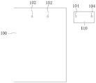
- Display screen 100 layer structure 10, light-transmitting area 101, base layer 11, masking layer 12, display area 121, first area 122, second area 123, pixel 124, non-display area 125, organic film layer 13, polarizing layer 14 , The cover plate 15, the microlens 20, the connecting portion 21, the first positioning structure 102, and the second positioning structure 104;
- Display assembly 200 image sensor 110, circuit board 111, photosensitive chip 112, flexible circuit board 113, groove 114, connector 120;
- Electronic device 300 housing 310.
- the solution for the under-screen camera of an electronic device such as a mobile phone is generally to arrange the camera as a whole under the display screen.
- the camera includes a lens and an image sensor.
- the thickness of the lens is relatively high, so that the overall thickness of the electronic device is relatively thick. For this reason, in order to reduce the overall thickness of the electronic device, it is generally necessary to hollow out or slot the display screen, and make the camera extend into the hole or slot to reduce the thickness of the electronic device.
- the thickness of the electronic device is still relatively large, and the overall structure of the display screen needs to be destroyed, which makes the manufacturing process difficult.
- an embodiment of the present application provides a display screen 100.
- the display screen 100 includes a layer structure 10 and a plurality of microlenses 20, and the plurality of microlenses 20 are embedded in the layer structure 10.
- the layer structure 10 includes a light-transmitting base layer 11 and a masking layer 12 formed on the base layer 11, and the masking layer 12 has a light-transmitting area 101.
- the microlens 20 is arranged corresponding to the light-transmitting area 101, and the plurality of microlenses 20 are used to image the target object on the image sensor 110 on the side of the base layer 11 away from the masking layer 12 through the plurality of light-transmitting areas 101.
- the display screen 100 of the embodiment of the present application can be applied to the display assembly 200 and the electronic device 300.
- the display assembly 200 includes an image sensor 110 and the aforementioned display screen 100, and the display screen 100 covers the image sensor 110.
- the display assembly 200 is located on the front side of the electronic device 300.
- the electronic device 300 includes a housing 310, and the display assembly 200 is disposed in the housing 310.
- the display assembly 200 may be fixed to the housing 310 through a glue dispensing process.
- the housing 310 is a support of the electronic device 300 and is used to support the components of the electronic device 300.
- the housing 310 can also reduce the impact of internal components of the electronic device 300.
- the plurality of microlenses 20 are used to image a target object on the image sensor 110 located on the side of the thickness direction of the display screen 100 through the plurality of light-transmitting regions 101. This can not only ensure that the electronic device 300 has a front camera function, but also can increase the screen-to-body ratio of the electronic device 300.
- the use of the microlens 20 for imaging can reduce the thickness of the display assembly 200 and the electronic device 300 and improve the user experience.
- microlenses 20 are embedded in the layer structure 10, so that there is no need to destroy the structure of the display screen 100 after the display screen 100 is manufactured, and the manufacturing process is less difficult.
- the screen-to-body ratio of the electronic device 300 refers to the ratio of the area of the front surface of the electronic device 300 corresponding to the display area of the display screen 100 on the front surface of the electronic device 300 to other areas of the front surface. Increasing the screen-to-body ratio of the electronic device 300 can improve the visual effect of the electronic device 300, thereby improving user experience.
- the display screen 100 covering the image sensor 110 means that the orthographic projection of the image sensor 110 on the lower surface of the display screen 100 is located in the lower surface.
- the plurality of microlenses 20 may be arranged in a horizontal direction, or may be arranged in an oblique direction.
- each microlens 20 can form an image on the image sensor 110. Therefore, the image sensor 110 can collect multiple images formed by multiple microlenses 20. After processing the multiple images collected by the image sensor 110, it can be completed. Image.
- the number of microlenses 20 is five. Therefore, the image sensor 110 first collects five partial images, and after processing, a complete image is obtained.
- the number of microlenses 20 is five. Therefore, the image sensor 110 first collects five partial images, and after processing, a complete image is obtained.
- microlens 20 there may be one microlens 20, or a plurality of stacked microlenses. In the embodiment shown in FIG. 4, in the thickness of the display screen 100, two microlenses 20 are stacked. In other embodiments, the number of microlenses 20 may be three or more.
- the layer structure 10 has multiple layers. For example, one of the layers is used to generate light so that the display screen 100 can display pictures. For example, the other layer is used to filter certain wavelengths of light in natural light. (E.g. UV).
- natural light E.g. UV
- the display screen 100 may be an Organic Light-Emitting Diode (OLED) display screen 100.
- OLED Organic Light-Emitting Diode
- the OLED display screen 100 has good light transmittance and can pass visible light and infrared light. Therefore, the OLED display screen 100 does not affect the image sensor 110 to receive light when displaying content effects.
- the display screen 100 may also be a Micro LED display screen 100.
- the electronic device 300 may be any of various types of computer system devices that are mobile or portable and perform wireless communication (only one form is exemplarily shown in FIG. 2).
- the electronic device 300 may be a mobile phone or a smart phone, for example, a phone based on the iPhone system (Apple system), a phone based on the Android system (Android system), a portable game device (such as an iPhone (Apple mobile phone), a laptop computer, Personal digital assistants (PDAs), portable Internet devices, music players, and data storage devices, other handheld devices, such as watches, and the electronic device 300 can also be other wearable devices (for example, smart glasses, smart watches, Or head mount display (HMD)).
- HMD head mount display
- the image sensor 110 includes a circuit board 111 and a photosensitive chip 112.
- the photosensitive chip 112 is arranged on the circuit board 111.
- the photosensitive chip 112 is fixed on the circuit board 111 through a surface mount process.
- the multiple microlens 20 arrays are used to image the target object on the photosensitive chip 112 through the multiple light-transmitting regions 101.
- the circuit board 111 may be a rigid circuit board or a flexible circuit board.
- the circuit board 111 is a rigid circuit board.
- the circuit board 111 is a printed circuit board (Printed Circuit Board, PCB).
- the display assembly 200 further includes a flexible circuit board 113, and the flexible circuit board 113 is connected to the circuit board 111.
- the flexible circuit board 113 may be connected to the main board of the electronic device 300 to implement communication with the main board of the electronic device 300.
- the photosensitive chip 112 is a die.
- the photosensitive chip 112 may be a complementary metal oxide semiconductor (Complementary Metal Oxide Semiconductor, CMOS) photosensitive element or a charge-coupled device (Charge-coupled Device, CCD) photosensitive element.
- CMOS Complementary Metal Oxide Semiconductor
- CCD Charge-coupled Device
- the photosensitive chip 112 can be electrically connected to the circuit board 111 through a gold wire.
- the gold wires can be packaged by a packaging material to prevent the gold wires from breaking and improve the stability of the image sensor 110.
- the circuit board 111 is formed with a groove 114, and the photosensitive chip 112 is received in the groove 114.
- the overall thickness of the image sensor 110 is relatively thin, which is beneficial to reduce the thickness of the display assembly 200.
- a plurality of microlenses 20 are located on the side of the masking layer 12 away from the base layer 11.
- the base layer 11 may be made of rigid materials such as glass, or may be made of flexible materials such as organic materials.
- the masking layer 12 may be provided with display pixels and traces of the display screen 100.
- the masking layer 12 may be formed on the base layer 11 through a photolithography process. As shown in the orientation of FIG. 5, a plurality of microlenses 20 are located above the masking layer 12.
- the masking layer 12 can also be formed by wafer growth, deposition, etching, or the like.
- the microlens 20 can be bonded to one side of the masking layer 12 by optical glue, and the microlens 20 can also be formed on one side of the display screen 100 by a wafer level optics.
- the layer structure 10 further includes an organic film layer 13 covering the masking layer 12, and a plurality of microlenses 20 are sandwiched between the organic film layer 13 and the masking layer 12.
- the organic film layer 13 can protect the plurality of microlenses 20 and the masking layer 12 and prevent impurities such as moisture and dust from entering the masking layer 12.
- the organic film layer 13 is made of, for example, polyimide (PI), which not only makes the organic film layer 13 more flexible, but also makes the thickness of the organic film layer 13 lower, effectively reducing the thickness of the display screen 100 .
- PI polyimide
- the layer structure 10 further includes a polarizing layer 14 stacked with the organic film layer 13, and the polarizing layer 14 is located on the side of the organic film layer 13 away from the masking layer 12.
- the polarizing layer 14 can filter natural light entering the light of a specific vibration direction in the display screen 100, and prevent the display screen 100 from reflecting the light and reducing the display effect of the display screen 100.
- the display screen 100 further includes a cover plate 15 located on a side of the polarizing layer 14 away from the organic film layer 13.
- the cover plate 15 and the polarizing layer 14 are stacked to cover the polarizing layer 14.
- the cover plate 15 is made of, for example, a high-transmittance material such as glass.
- the cover 15 can protect the display screen 100 and increase the life span of the display screen 100.
- the cover 15 can be fixedly connected to the polarizing layer 14 by optical glue.
- the base layer 11, the organic film layer 13, the polarizing layer 14, and the cover plate 15 are all light-transmissive. Therefore, light can pass through these layer elements to reach the image sensor 110.
- the masking layer 12 includes a display area 121, and the display area 121 includes a first area 122 and a second area 123, and the second area 123 is connected to the first area 122. Pixel arrays are distributed in both the first area 122 and the second area 123.
- the light-transmitting area 101 is located between adjacent pixels 124 in the first area of the display area 121.
- the light-transmitting area 101 is located between two adjacent pixels 124, which can prevent the light-transmitting area 101 from interfering with the pixels 124, making the light-transmitting area 101 easier to form, and facilitating the image sensor 110 to collect images of the target object.
- the pixel density of the first area 122 is less than the pixel density of the second area 123. It can be understood that the pixel density refers to the ratio of the number of pixels per unit area to the area. In this way, the light-transmitting area 101 can be formed more easily between the adjacent pixels 124 of the first area 122, and since the pixels 124 of the first area 122 are less, the light generated by the pixels 124 of the first area 122 affects the image sensor 110. The influence of imaging interference is low, which is beneficial to improve the imaging quality of the image sensor 110.
- the edges of the layer structure 10 can be glued together, and there are no pixels on the edges of the layer structure 10. Therefore, a non-display area 125 is formed at the edge of the display screen 100, and a display area 121 is formed in the middle part of the display screen 100. As shown in FIG.
- the display area 121 may have a shape such as a right-angled rectangle or a rounded rectangle.
- the non-display area 125 has a frame shape.
- the mask layer 12 (mask) has pixels 124 to display a picture
- the mask layer 12 may also be referred to as a display layer.
- first and second mentioned here are only used for descriptive purposes, and cannot be understood as indicating or implying relative importance or implicitly indicating the number of indicated technical features. Thus, the features defined with “first” and “second” may explicitly or implicitly include one or more features. In the description of the present application, "a plurality of” means two or more than two, unless otherwise specifically defined.
- the display screen 100 includes a layer structure 10 and a plurality of microlenses 20, and the layer structure 10 includes a light-transmissive base layer 11 and a masking layer 12 formed on the base layer 11.
- the masking layer 12 has a light-transmitting area 101.
- the display area 121 includes a first area 122 and a second area 123, and both the first area 122 and the second area 123 are distributed with pixel arrays.
- the light-transmitting area 101 is located between adjacent pixels 124 in the first area of the display area 121.
- the pixel density of the first area 122 is smaller than the pixel density of the second area 123.
- the microlens 20 is arranged corresponding to the light-transmitting area 101, and the plurality of microlenses 20 are used to image the target object on the image sensor 110 on the side of the base layer 11 away from the masking layer 12 through the plurality of light-transmitting areas 101.
- a plurality of microlenses 20 are sandwiched between the base layer 11 and the masking layer 12. In this way, the microlens 20 can be imaged on the image sensor 110 through the base layer 11.
- the light-transmitting area 101 is a through hole formed on the masking layer 12. In other words, the light passes through the through hole of the masking layer 12 and the micro lens 20 and then strikes the image sensor 110.
- the light transmittance of the through hole is relatively large, so that the light loss can be reduced.
- the light-transmitting area 101 is a light-transmitting physical part formed on the masking layer 12.
- the light-transmitting area 101 may be made of a high light-transmitting material such as resin. The light transmittance of the light-transmitting area 101 is greater than 90%.
- the plurality of light-transmitting regions 101 are arranged in an array.
- the light-transmitting areas 101 may be arranged in a 6*6 matrix.
- the multiple light-transmitting areas 101 can be arranged in other ways.
- each light-transmitting area 101 is arranged corresponding to one of the microlenses 20.
- the light-transmitting area 101 and the microlens 20 have a one-to-one correspondence.
- the number of light-transmitting regions 101 is 36, arranged in a 6*6 matrix; the number of microlenses 20 is also 36, and arranged in a 6*6 matrix, as shown in FIG. 9.
- the lateral dimension of the light-transmitting area 101 is less than 0.5 mm.
- the radial dimension of the light-transmitting area 101 is less than 0.5 mm.
- the lateral dimension of the microlens 20 is less than 0.5 mm; when the lateral cross section of the microlens 20 is circular, the radial dimension of the microlens 20 is less than 0.5 mm.
- the display assembly 200 includes a connector 120, and the connector 120 is connected to the image sensor 110 and the display screen 100.
- the image sensor 110 can be fixed to the display screen 100 through the connecting member 120, so that the display assembly 200 forms a whole, which facilitates the installation of the display assembly 200 to the housing 310 of the electronic device 300.
- the above connecting member 120 includes glue, and the glue is used to bond the image sensor 110 and the display screen 100.
- the viscose is, for example, a colloid such as silicone glue.
- adhesive is used to bond the image sensor 110 and the display screen 100, so that the connection between the image sensor 110 and the display screen 100 is more stable, and the process is simple.
- the circuit board 111 and the display screen 100 are glued together. It should be pointed out that when the display screen 100 also includes a shielding layer and a foam buffer layer, the glue is connected to the layer of the display screen 100 close to the image sensor 110.
- the glue seals the gap between the image sensor 110 and the display screen 100.
- the glue can prevent foreign matter such as dust and moisture from entering the photosensitive chip 112 and affect the normal operation of the photosensitive chip 112. Suffice it to say that the adhesive surrounds the photosensitive chip 112.
- the display screen 100 is provided with a first positioning structure 102
- the image sensor 110 is provided with a second positioning structure 104
- the image sensor 110 passes through the first positioning structure 102 and the second positioning structure 102.
- the positioning structure 104 is coordinated and positioned on the display screen 100.
- the first positioning structure 102 and the second positioning structure 104 enable the image sensor 110 to be accurately positioned on the display screen 100 and ensure that the microlens 20 corresponds to the light-transmitting area 101.
- the first positioning structure 102 is a positioning groove
- the second positioning structure 104 is a protrusion
- the protrusion is inserted into the positioning groove, so that the image sensor 110 and the display screen 100 are positioned and connected.
- the display assembly 200 includes a light guide element 130 disposed between the display screen 100 and the image sensor 110, and the light guide element 130 is used to guide the light passing through the light transmission area 101 to the image sensor 110.
- the light guide element 130 can cause the light to be transmitted to the microlens 20 more concentratedly, which facilitates imaging of the microlens 20, so that the image sensor 110 can obtain a better quality external image.
- the light guide element 130 may be made of a material with high light transmittance such as polyester, so as to reduce the light loss of the light guide element 130 during the light guide process.
- the light guide element 130 may be columnar, or may be bent or the like. When the light guide element 130 is in a bent shape, the image sensor 110 and the plurality of light-transmitting regions 101 may be offset.
- the light guide element can be fixed on the display screen 100 by optical glue bonding, so that the position of the light guide element is fixed.
- a plurality of microlenses 20 are connected by a connecting portion 21.
- the connecting portion 21 and the micro lens 20 are an integral structure.
- Both the microlens 20 and the connecting portion 21 are made of, for example, a material with high light transmittance such as resin. It can be understood that the microlens 20 has a curved surface, so that the microlens 20 can perform light focusing and imaging.
- the description with reference to the terms “one embodiment”, “certain embodiments”, “exemplary embodiments”, “examples”, “specific examples”, or “some examples” etc. means to combine The specific features, structures, materials or characteristics described in the embodiments or examples are included in at least one embodiment or example of the present application.
- the schematic representation of the above-mentioned terms does not necessarily refer to the same embodiment or example.
- the described specific features, structures, materials or characteristics can be combined in any one or more embodiments or examples in a suitable manner.
Landscapes
- Engineering & Computer Science (AREA)
- Signal Processing (AREA)
- Devices For Indicating Variable Information By Combining Individual Elements (AREA)
- Studio Devices (AREA)
Abstract
Description
本申请涉及电子设备领域,尤其涉及一种显示屏、显示组件和电子装置。This application relates to the field of electronic equipment, and in particular to a display screen, a display assembly and an electronic device.
随着手机技术的发展和用户的需求,全面屏手机已经成为手机的发展趋势。在相关技术中,手机设置有前置摄像头,手机的显示屏形成有避让前置摄像头的槽或孔,以使前置摄像头可以采集外部图像。然而,显示屏形成的槽或孔使得手机的屏占比降低,因此,如何使手机具有前置拍摄功能并提高手机的屏占比成为待解决的技术问题。With the development of mobile phone technology and the needs of users, full-screen mobile phones have become the development trend of mobile phones. In related technologies, the mobile phone is provided with a front camera, and the display screen of the mobile phone is formed with a slot or hole that avoids the front camera, so that the front camera can collect external images. However, the grooves or holes formed by the display screen reduce the screen-to-body ratio of the mobile phone. Therefore, how to make the mobile phone have a front-shooting function and increase the screen-to-body ratio of the mobile phone has become a technical problem to be solved.
发明内容Summary of the invention
本申请提供一种显示屏、显示组件和电子装置。The application provides a display screen, a display assembly, and an electronic device.
本申请实施方式提供了一种显示屏,显示屏包括层结构和多个微透镜,所述层结构包括透光的基层和形成在所述基层上掩盖层,所述掩盖层具有多个透光区。多个微透镜嵌设在所述层结构内,所述微透镜与所述透光区相应设置,所述多个微透镜用于通过所述多个透光区将目标物体成像于位于所述显示屏厚度方向一侧的图像传感器。The embodiment of the present application provides a display screen. The display screen includes a layer structure and a plurality of microlenses. The layer structure includes a light-transmitting base layer and a masking layer formed on the base layer. The masking layer has a plurality of light-transmitting lenses. Area. A plurality of microlenses are embedded in the layer structure, the microlenses are arranged corresponding to the light-transmitting area, and the plurality of microlenses are used to image a target object in the light-transmitting area through the plurality of light-transmitting areas. The image sensor on the side of the thickness of the display.
本申请实施方式的显示屏包括:The display screen of the embodiment of the present application includes:
层结构,所述层结构包括透光的基层和形成在所述基层上掩盖层,所述掩盖层具有多个透光区;和A layer structure, the layer structure comprising a light-transmitting base layer and a masking layer formed on the base layer, the masking layer having a plurality of light-transmitting regions; and
嵌设在所述层结构内的多个微透镜,所述微透镜与所述透光区相应设置,所述多个微透镜用于通过所述多个透光区将目标物体成像于位于所述显示屏厚度方向一侧的图像传感器。A plurality of microlenses embedded in the layer structure, the microlenses are arranged corresponding to the light-transmitting area, and the plurality of microlenses are used to image a target object in the light-transmitting area through the plurality of light-transmitting areas. The image sensor on one side of the thickness direction of the display screen.
本申请实施方式的显示屏组件包括:The display screen assembly of the embodiment of the present application includes:
图像传感器;和Image sensor; and
遮盖所述图像传感器的显示屏,所述显示屏包括:A display screen covering the image sensor, the display screen comprising:
层结构,所述层结构包括透光的基层和形成在所述基层上掩盖层,所述掩盖层具有多个透光区;和A layer structure, the layer structure comprising a light-transmitting base layer and a masking layer formed on the base layer, the masking layer having a plurality of light-transmitting regions; and
嵌设在所述层结构内的多个微透镜,所述微透镜与所述透光区相应设置,所述多个微透镜用于通过所述多个透光区将目标物体成像于所述图像传感器。A plurality of microlenses embedded in the layer structure, the microlenses are arranged corresponding to the light-transmitting area, and the plurality of microlenses are used to image a target object on the light-transmitting area through the plurality of light-transmitting areas. Image Sensor.
本申请实施方式的电子装置包括以上所述的显示组件和壳体,所述显示组件设置在所述壳体。The electronic device of the embodiment of the present application includes the above-mentioned display assembly and a housing, and the display assembly is provided in the housing.
本申请实施方式的显示屏、显示组件和电子装置中,所述多个微透镜用于通过所述多个透光区将目标物体成像于位于所述显示屏厚度方向一侧的图像传感器,这样不仅可以保证电子装置具有前置拍摄功能的同时可以提高电子装置的屏占比。另外,使用微透镜成像,如此可以降低显示组件和电子装置的厚度,提高用户体验。In the display screen, display assembly, and electronic device of the embodiments of the present application, the plurality of microlenses are used to image a target object on the image sensor located on one side of the thickness direction of the display screen through the plurality of light-transmitting areas. It can not only ensure that the electronic device has the front-shooting function, but also increase the screen-to-body ratio of the electronic device. In addition, the use of micro-lens for imaging can reduce the thickness of the display assembly and the electronic device and improve the user experience.
本申请的附加方面和优点将在下面的描述中部分给出,部分将从下面的描述中变得明显,或通过本申请的实践了解到。The additional aspects and advantages of the present application will be partly given in the following description, and part of them will become obvious from the following description, or be understood through the practice of the present application.
本申请的上述和/或附加的方面和优点从结合下面附图对实施方式的描述中将变得明显和容易理解,其中:The above and/or additional aspects and advantages of the present application will become obvious and easy to understand from the description of the embodiments in conjunction with the following drawings, in which:
图1是本申请实施方式的显示组件的剖面示意图;FIG. 1 is a schematic cross-sectional view of a display assembly according to an embodiment of the present application;
图2是本申请实施方式的电子装置的平面示意图;2 is a schematic plan view of an electronic device according to an embodiment of the present application;
图3是本申请实施方式的图像处理过程示意图;Fig. 3 is a schematic diagram of an image processing process of an embodiment of the present application;
图4是本申请实施方式的另一个图像处理过程示意图;FIG. 4 is a schematic diagram of another image processing process according to an embodiment of the present application;
图5是本申请实施方式的显示组件的另一剖面示意图;FIG. 5 is another schematic cross-sectional view of the display assembly of the embodiment of the present application;
图6是本申请实施方式的显示屏的掩盖层的结构示意图;6 is a schematic diagram of the structure of the masking layer of the display screen according to the embodiment of the present application;
图7是本申请实施方式的显示组件的再一剖面示意图;FIG. 7 is another schematic cross-sectional view of the display assembly of the embodiment of the present application;
图8是本申请实施方式的显示屏和图像传感器的分解示意图;FIG. 8 is an exploded schematic diagram of a display screen and an image sensor according to an embodiment of the present application;
图9是本申请实施方式的微透镜的立体示意图。FIG. 9 is a three-dimensional schematic diagram of a microlens according to an embodiment of the present application.
主要元件符号说明:Symbol description of main components:
显示屏100、层结构10、透光区101、基层11、掩盖层12、显示区121、第一区域122、第二区域123、像素124、非显示区125、有机膜层13、偏光层14、盖板15、微透镜20、连接部21、第一定位结构102、第二定位结构104;
显示组件200、图像传感器110、电路板111、感光芯片112、柔性电路板113、凹槽114、连接件120;
电子装置300、壳体310。
下面详细描述本申请的实施方式,所述实施方式的示例在附图中示出,其中自始至终相同或类似的标号表示相同或类似的元件或具有相同或类似功能的元件。下面通过参考附图描述的实施方式是示例性的,仅用于解释本申请,而不能理解为对本申请的限制。The embodiments of the present application are described in detail below. Examples of the embodiments are shown in the accompanying drawings, in which the same or similar reference numerals indicate the same or similar elements or elements with the same or similar functions. The following embodiments described with reference to the drawings are exemplary, and are only used to explain the present application, and should not be understood as a limitation to the present application.
下文的公开提供了许多不同的实施方式或例子用来实现本申请的不同结构。为了简化本申请的公开,下文中对特定例子的部件和设置进行描述。当然,它们仅仅为示例,并且目的不在于限制本申请。此外,本申请可以在不同例子中重复参考数字和/或参考字母,这种重复是为了简化和清楚的目的,其本身不指示所讨论各种实施方式和/或设置之间的关系。此外,本申请提供了的各种特定的工艺和材料的例子,但是本领域普通技术人员可以意识到其他工艺的应用和/或其他材料的使用。The following disclosure provides many different embodiments or examples for realizing different structures of the present application. In order to simplify the disclosure of the present application, the components and settings of specific examples are described below. Of course, they are only examples, and are not intended to limit the application. In addition, the present application may repeat reference numerals and/or reference letters in different examples. Such repetition is for the purpose of simplification and clarity, and does not indicate the relationship between the various embodiments and/or settings discussed. In addition, this application provides examples of various specific processes and materials, but those of ordinary skill in the art may be aware of the application of other processes and/or the use of other materials.
在相关技术中,手机等电子装置的屏下摄像头的方案一般是将摄像头整体设置在显示屏的下方,摄像头包括镜头和图像传感器,镜头的厚度较高,因此使得电子装置的整体厚度较厚。为此,为了降低电子装置的整体厚度,一般需显示屏上挖空或开槽,并且使摄像头伸入改孔或槽中,以降低电子装置的厚度。但是这种方案中,电子装置的厚度仍然较大,并且需要破坏显示屏的整体结构,制作工艺难度大。In the related art, the solution for the under-screen camera of an electronic device such as a mobile phone is generally to arrange the camera as a whole under the display screen. The camera includes a lens and an image sensor. The thickness of the lens is relatively high, so that the overall thickness of the electronic device is relatively thick. For this reason, in order to reduce the overall thickness of the electronic device, it is generally necessary to hollow out or slot the display screen, and make the camera extend into the hole or slot to reduce the thickness of the electronic device. However, in this solution, the thickness of the electronic device is still relatively large, and the overall structure of the display screen needs to be destroyed, which makes the manufacturing process difficult.
请参阅图1,本申请实施方式提供了一种显示屏100,显示屏100包括层结构10和多个微透镜20,多个微透镜20嵌设在层结构10内。层结构10包括透光的基层11和形成在基层11上掩盖层12,掩盖层12具有透光区101。微透镜20与透光区101相应设置,多个微透镜20用于通过多个透光区101将目标物体成像于位于基层11背离掩盖层12一侧的图像传感器110上。Referring to FIG. 1, an embodiment of the present application provides a
请参阅图2,本申请实施方式的显示屏100可以应用于显示组件200和电子装置300。显示组件200包括图像传感器110和以上所说的显示屏100,显示屏100遮盖图像传感器110。Please refer to FIG. 2, the
可以理解,显示组件200位于电子装置300的前侧。具体地,电子装置300包括壳体310,显示组件200设置在壳体310。例如,显示组件200可以通过点胶的工艺与壳体310固定。壳体310为电子装置300的支撑件,其用于支撑电子装置300的零部件。壳体310还可以减少电子装置300的内部零部件受到冲击。It can be understood that the
本申请实施方式的显示屏100、显示组件200和电子装置300中,多个微 透镜20用于通过多个透光区101将目标物体成像于位于显示屏100厚度方向一侧的图像传感器110,这样不仅可以保证电子装置300具有前置拍摄功能的同时可以提高电子装置300的屏占比。另外,使用微透镜20成像,如此可以降低显示组件200和电子装置300的厚度,提高用户体验。In the
还有微透镜20嵌设在层结构10内,这样无需在显示屏100制造形成后再破坏显示屏100的结构,制造工艺难度较低。Furthermore, the
可以理解,电子装置300的屏占比指的是,电子装置300的前表面中,电子装置300的前表面中显示屏100的显示区域对应的区域与前表面的其他区域的面积比值。提高电子装置300的屏占比可以提高电子装置300的视觉效果,从而提高用户体验。It can be understood that the screen-to-body ratio of the
需要指出的是,显示屏100遮盖图像传感器110指的是,图像传感器110在显示屏100的下表面的正投影位于下表面内。多个微透镜20可以沿水平方向排布,也可以沿倾斜的方向排布。It should be noted that the
可以理解,每个微透镜20可以在图像传感器110形成一个像,因此,图像传感器110可以采集多个微透镜20形成的多个像,经过处理图像传感器110采集的多个像后,可以得到完成的图像。It can be understood that each microlens 20 can form an image on the
在一个例子中,请参阅图3,微透镜20的数量为5个,因此,图像传感器110首先采集到5个局部图像,经过处理后,得到一个完整的图像。In an example, referring to FIG. 3, the number of
在另一个例子中,请参阅图4,微透镜20的数量为5个,因此,图像传感器110首先采集到5个局部图像,经过处理后,得到一个完整的图像。In another example, referring to FIG. 4, the number of
需要指出的是,在显示屏100的厚度上,微透镜20可以为一个,也可以为堆叠设置的多个。如图4的实施方式中,在显示屏100的厚度上,微透镜20为堆叠设置的两个。在其他实施方式中,微透镜20可以为3个或者3个以上。It should be pointed out that, in the thickness of the
层结构10具有多个层,例如,其中一个层的作用是用于产生光线以使显示屏100可以显示画面,又如,另外一个层的作用是用于过滤自然光中的某些特定波长的光线(例如紫外线)。The
本实施方式中,显示屏100可以是有机发光二极管(Organic Light-Emitting Diode,OLED)显示屏100,OLED显示屏100具有良好的透光性,能够通过可见光和红外光。因此,OLED显示屏100在展现内容效果的情况下也不影响图像传感器110接收光线。显示屏100也可以采用Micro LED显示屏100。In this embodiment, the
本实施方式中,示例性地,电子装置300可以为移动或便携式并执行无线 通信的各种类型的计算机系统设备中的任何一种(图2中只示例性的示出了一种形态)。具体的,电子装置300可以为移动电话或智能电话,例如,基于iPhone system(苹果系统),基于Android system(安卓系统)的电话,便携式游戏设备(例如iPhone(苹果手机)、膝上型电脑、掌上电脑(personal digital assistant,PDA)、便携式互联网设备、音乐播放器以及数据存储设备,其他手持设备以及诸如手表,电子装置300还可以为其他的可穿戴设备(例如,诸如智能眼镜、智能手表、或者头戴式设备(head mount display,HMD))。In this embodiment, for example, the
具体地,请参阅图5,图像传感器110包括电路板111和感光芯片112。感光芯片112设置在电路板111上。例如,感光芯片112通过表面贴装的工艺固定在电路板111上。多个微透镜20阵列用于通过多个透光区101将目标物体成像在感光芯片112上。Specifically, referring to FIG. 5, the
电路板111可以为刚性电路板,也可以为柔性电路板。本实施方式中,电路板111为刚性电路板。例如,电路板111为印刷电路板(Printed Circuit Board,PCB)。进一步地,在电路板111为刚性电路板时,显示组件200还包括柔性电路板113,柔性电路板113与电路板111连接。柔性电路板113可以与电子装置300的主板连接,以与电子装置300的主板实现通信。The
感光芯片112为裸片(die)。感光芯片112可以采用互补金属氧化物半导体(Complementary Metal Oxide Semiconductor,CMOS)感光元件或者电荷耦合元件(Charge-coupled Device,CCD)感光元件。The
感光芯片112可以通过金线与电路板111实现电性连接。在一个例子中,感光芯片112和电路板111打金线连接后,可以通过封装材料将金线封装,以防止金线断裂,提高了图像传感器110的稳定性。The
进一步地,电路板111形成有凹槽114,感光芯片112收容于凹槽114内。如此,图像传感器110的整体厚度较薄,有利于减低显示组件200的厚度。Furthermore, the
请参阅图5,在一些实施方式中,多个微透镜20位于掩盖层12背离基层11的一侧。Referring to FIG. 5, in some embodiments, a plurality of
具体地,基层11可以采用玻璃等刚性材料制成,也可以采用有机材料等柔性材料制成。掩盖层12可以设置有显示屏100的显示像素和走线。掩盖层12可以通过光刻工艺形成在基层11上。如图5的方位所示,多个微透镜20位于掩盖层12的上方。可选地,该掩盖层12还可以通过晶圆生长、沉积、蚀刻等方式成型。Specifically, the
微透镜20可以通过光学胶粘接在掩盖层12的一面,微透镜20也可以通 过晶圆封装方式的工艺(wafer level optics)形成于显示屏100的一面。The
请参阅图5,在一些实施方式中,层结构10还包括覆盖掩盖层12的有机膜层13,多个微透镜20夹设于有机膜层13和掩盖层12之间。如此,有机膜层13可以保护多个微透镜20和掩盖层12,防止水汽、灰尘等杂质进入掩盖层12中。有机膜层13例如采用聚酰亚胺(PI)制成,这样不仅可以使得有机膜层13的韧性较好,还可以使得有机膜层13的厚度较低,有效地降低了显示屏100的厚度。Referring to FIG. 5, in some embodiments, the
请参阅图5,在一些实施方式中,层结构10还包括与有机膜层13堆叠设置的偏光层14,偏光层14位于有机膜层13背离掩盖层12的一侧。如此,偏光层14可以过滤自然光进入显示屏100中特定振动方向的光线,避免显示屏100反射该光线而降低显示屏100的显示效果。Referring to FIG. 5, in some embodiments, the
请参阅图5,在一些实施方式中,显示屏100还包括位于偏光层14背离有机膜层13的一侧的盖板15。或者说,盖板15与偏光层14层叠设置并覆盖偏光层14。盖板15例如采用玻璃等高透光材料制成。盖板15可以保护显示屏100,提高显示屏100的寿命。盖板15可以通过光学胶与偏光层14固定连接。Referring to FIG. 5, in some embodiments, the
需要指出的是,基层11、有机膜层13、偏光层14和盖板15,这些层元件整体均是透光的,因此,光线可以透过这些层元件到达图像传感器110。It should be pointed out that the
请参阅图6,在一些实施方式中,掩盖层12包括显示区121,显示区121包括第一区域122和第二区域123,第二区域123与第一区域122连接。第一区域122和第二区域123均分布像素阵列。透光区101位于显示区121的第一区域的相邻像素124之间。Referring to FIG. 6, in some embodiments, the
如此,透光区101位于相邻的两个像素124之间,这样可以防止透光区101与像素124干涉,使得透光区101更加容易形成,便于图像传感器110采集目标物体图像。In this way, the light-transmitting
进一步地,第一区域122的像素密度小于第二区域123的像素密度。可以理解,像素密度指的是单位面积内的像素数量与面积的比值。如此,在第一区域122的相邻像素124之间可以更加容易形成透光区101,并且由于第一区域122的像素124更少,第一区域122的像素124产生的光线对图像传感器110的成像干扰影响较低,有利于提高图像传感器110的成像品质。Further, the pixel density of the
可以理解,由于显示屏100具有层结构10,层结构10的边缘可以通过粘胶粘贴一起,在层结构10的边缘没有像素。因此,在显示屏100的边缘形成 有非显示区125,显示屏100的中间部分形成显示区121。It can be understood that since the
显示区121可以呈直角矩形或圆角矩形等形状。非显示区125呈框形。The
由于掩盖层12(mask)具有像素124以显示画面,因此,掩盖层12也可以称为显示层。Since the mask layer 12 (mask) has
此处所说的“第一”、“第二”仅用于描述目的,而不能理解为指示或暗示相对重要性或者隐含指明所指示的技术特征的数量。由此,限定有“第一”、“第二”的特征可以明示或者隐含地包括一个或者更多个特征。在本申请的描述中,“多个”的含义是两个或两个以上,除非另有明确具体的限定。The "first" and "second" mentioned here are only used for descriptive purposes, and cannot be understood as indicating or implying relative importance or implicitly indicating the number of indicated technical features. Thus, the features defined with "first" and "second" may explicitly or implicitly include one or more features. In the description of the present application, "a plurality of" means two or more than two, unless otherwise specifically defined.
在一些实施方式中,显示屏100包括层结构10和多个微透镜20,层结构10包括透光的基层11和形成在基层11上掩盖层12。掩盖层12具有透光区101。显示区121包括第一区域122和第二区域123,第一区域122和第二区域123均分布像素阵列。透光区101位于显示区121的第一区域的相邻像素124之间。第一区域122的像素密度小于第二区域123的像素密度。微透镜20与透光区101相应设置,多个微透镜20用于通过多个透光区101将目标物体成像于位于基层11背离掩盖层12一侧的图像传感器110上。In some embodiments, the
如图7所示,在一些实施方式中,多个微透镜20夹设在基层11和掩盖层12之间。这样可以使得微透镜20可以通过基层11成像于图像传感器110。As shown in FIG. 7, in some embodiments, a plurality of
在一些实施方式中,透光区101为形成于掩盖层12上的通孔。或者说,光线通过掩盖层12的通孔和微透镜20后射至图像传感器110。通孔的透光率较大,这样可以减少光的损耗。当然,在一些实施方式中,透光区101为形成于掩盖层12的透光实体部分。例如,透光区101可以采用树脂等高透光材料制成。透光区101的透光率大于90%。In some embodiments, the light-transmitting
在一些实施方式中,多个透光区101呈阵列排布。例如,透光区101可以呈6*6矩阵排布。当然,多个透光区101可以呈其他方式排布。In some embodiments, the plurality of light-transmitting
在一些实施方式中,每个透光区101与其中一个微透镜20对应设置。或者说,透光区101和微透镜20为一一对应的关系。在一个例子中,透光区101的数量为36个,并呈6*6矩阵排布;微透镜20的数量也为36个,并呈6*6矩阵排布,如图9所示。In some embodiments, each light-transmitting
在一些实施方式中,透光区101的横向尺寸小于0.5mm。透光区101呈柱状时,透光区101的径向尺寸小于0.5mm。相应地,微透镜20的横向尺寸小于0.5mm;在微透镜20的横向截面呈圆形时,微透镜20的径向尺寸小于0.5mm。In some embodiments, the lateral dimension of the light-transmitting
请参阅图5,在一些实施方式中,显示组件200包括连接件120,连接件120与图像传感器110及显示屏100连接。如此,图像传感器110可以通过连接件120与显示屏100固定,使得显示组件200形成一个整体,有利于显示组件200安装至电子装置300的壳体310。Please refer to FIG. 5. In some embodiments, the
具体地,在一个例子中,以上的连接件120包括粘胶,粘胶粘接图像传感器110及显示屏100。粘胶例如为硅酮胶等胶体。如此,使用粘胶粘接图像传感器110和显示屏100,使得图像传感器110与显示屏100连接更加稳定,并且工艺简单。Specifically, in an example, the above connecting
可以理解,为了不影响图像传感器110采集目标物体图像,粘胶粘接电路板111和显示屏100。需要指出的是,显示屏100还包括有屏蔽层以及泡棉缓冲层等结构时,粘胶与显示屏100的靠近图像传感器110的层连接。It can be understood that, in order not to affect the
较佳地,粘胶密封图像传感器110与显示屏100之间的间隙。如此,粘胶可以防止灰尘、水汽等异物进入感光芯片112而影响感光芯片112正常工作。只要说明的是,粘胶环绕感光芯片112。Preferably, the glue seals the gap between the
为了便于图像传感器110设置在显示屏100,请参阅图8,显示屏100设置有第一定位结构102,图像传感器110设置有第二定位结构104,图像传感器110通过第一定位结构102与第二定位结构104配合定位在显示屏100。In order to facilitate the placement of the
如此,第一定位结构102和第二定位结构104使得图像传感器110设置在显示屏100的位置准确,保证微透镜20与透光区101对应。In this way, the
在一个例子中,第一定位结构102为定位槽,第二定位结构104为凸起,凸起插设于定位槽中,从而使得图像传感器110与显示屏100定位连接。In an example, the
在一些实施方式中,显示组件200包括设置在显示屏100和图像传感器110之间的导光元件130,导光元件130用于将通过透光区101的光线导向图像传感器110。In some embodiments, the
如此,导光元件130可以使得光线更加集中地传向微透镜20,有利于微透镜20成像,使得图像传感器110可以获取品质较佳的外部图像。In this way, the
导光元件130可以采用聚酯等透光率较高材料制成,以减少导光元件130在导光的过程中的光损耗。导光元件130可以呈柱状,也可以呈折弯等形状。在导光元件130呈折弯等形状时,图像传感器110与多个透光区101可以偏离设置。The
导光元件可以通过光学胶粘接固定在显示屏100上,从而使得导光元件的位置固定。The light guide element can be fixed on the
请参阅图9,在一些实施方式中,多个微透镜20通过连接部21连接。较佳地,连接部21与微透镜20为一体结构。微透镜20和连接部21例如均采用树脂等高透光率的材料制成。可以理解,微透镜20具有一曲面,以使微透镜20可以进行光线聚焦成像。Please refer to FIG. 9, in some embodiments, a plurality of
在本说明书的描述中,参考术语“一个实施方式”、“某些实施方式”、“示意性实施方式”、“示例”、“具体示例”、或“一些示例”等的描述意指结合所述实施方式或示例描述的具体特征、结构、材料或者特点包含于本申请的至少一个实施方式或示例中。在本说明书中,对上述术语的示意性表述不一定指的是相同的实施方式或示例。而且,描述的具体特征、结构、材料或者特点可以在任何的一个或多个实施方式或示例中以合适的方式结合。In the description of this specification, the description with reference to the terms “one embodiment”, “certain embodiments”, “exemplary embodiments”, “examples”, “specific examples”, or “some examples” etc. means to combine The specific features, structures, materials or characteristics described in the embodiments or examples are included in at least one embodiment or example of the present application. In this specification, the schematic representation of the above-mentioned terms does not necessarily refer to the same embodiment or example. Moreover, the described specific features, structures, materials or characteristics can be combined in any one or more embodiments or examples in a suitable manner.
尽管已经示出和描述了本申请的实施方式,本领域的普通技术人员可以理解:在不脱离本申请的原理和宗旨的情况下可以对这些实施方式进行多种变化、修改、替换和变型,本申请的范围由权利要求及其等同物限定。Although the embodiments of the present application have been shown and described, those of ordinary skill in the art can understand that various changes, modifications, substitutions, and modifications can be made to these embodiments without departing from the principle and purpose of the present application. The scope of the application is defined by the claims and their equivalents.
Claims (21)
Priority Applications (2)
| Application Number | Priority Date | Filing Date | Title |
|---|---|---|---|
| CN201980099169.8A CN114223190A (en) | 2019-09-29 | 2019-09-29 | Display screen, display assembly and electronic device |
| PCT/CN2019/109052 WO2021056540A1 (en) | 2019-09-29 | 2019-09-29 | Display screen, display assembly and electronic device |
Applications Claiming Priority (1)
| Application Number | Priority Date | Filing Date | Title |
|---|---|---|---|
| PCT/CN2019/109052 WO2021056540A1 (en) | 2019-09-29 | 2019-09-29 | Display screen, display assembly and electronic device |
Publications (1)
| Publication Number | Publication Date |
|---|---|
| WO2021056540A1 true WO2021056540A1 (en) | 2021-04-01 |
Family
ID=75166297
Family Applications (1)
| Application Number | Title | Priority Date | Filing Date |
|---|---|---|---|
| PCT/CN2019/109052 Ceased WO2021056540A1 (en) | 2019-09-29 | 2019-09-29 | Display screen, display assembly and electronic device |
Country Status (2)
| Country | Link |
|---|---|
| CN (1) | CN114223190A (en) |
| WO (1) | WO2021056540A1 (en) |
Cited By (2)
| Publication number | Priority date | Publication date | Assignee | Title |
|---|---|---|---|---|
| CN113691714A (en) * | 2021-08-24 | 2021-11-23 | 维沃移动通信(杭州)有限公司 | Electronic equipment |
| CN115915648A (en) * | 2021-08-03 | 2023-04-04 | 鹏鼎控股(深圳)股份有限公司 | Circuit board for lens module and manufacturing method thereof |
Citations (11)
| Publication number | Priority date | Publication date | Assignee | Title |
|---|---|---|---|---|
| US20070264002A1 (en) * | 2006-05-11 | 2007-11-15 | Jin Ho Lee | Camera Module and Mobile Terminal Having the Same |
| CN107743198A (en) * | 2017-10-27 | 2018-02-27 | 努比亚技术有限公司 | A kind of photographic method, terminal and storage medium |
| CN108174071A (en) * | 2018-01-23 | 2018-06-15 | 深圳市群晖智能科技股份有限公司 | A kind of low camera module for accounting for screen rate |
| CN108418928A (en) * | 2018-05-23 | 2018-08-17 | Oppo广东移动通信有限公司 | electronic device |
| CN109274789A (en) * | 2018-09-17 | 2019-01-25 | 深圳奥比中光科技有限公司 | Electronic equipment |
| CN109690564A (en) * | 2018-12-04 | 2019-04-26 | 深圳市汇顶科技股份有限公司 | Optical lens and preparation method thereof, fingerprint recognition mould group, mobile terminal |
| CN109743430A (en) * | 2019-03-14 | 2019-05-10 | Oppo广东移动通信有限公司 | Display module and electronic device |
| CN109981842A (en) * | 2019-03-14 | 2019-07-05 | Oppo广东移动通信有限公司 | Display module, electronic device and manufacturing method of display module |
| CN110012136A (en) * | 2019-04-02 | 2019-07-12 | 北京旷视科技有限公司 | Display device, display screen and terminal equipment |
| CN110088768A (en) * | 2019-03-12 | 2019-08-02 | 深圳市汇顶科技股份有限公司 | Under-screen fingerprint recognition device and electronic equipment |
| CN110266861A (en) * | 2019-07-23 | 2019-09-20 | 京东方科技集团股份有限公司 | display panel, display device |
-
2019
- 2019-09-29 WO PCT/CN2019/109052 patent/WO2021056540A1/en not_active Ceased
- 2019-09-29 CN CN201980099169.8A patent/CN114223190A/en active Pending
Patent Citations (11)
| Publication number | Priority date | Publication date | Assignee | Title |
|---|---|---|---|---|
| US20070264002A1 (en) * | 2006-05-11 | 2007-11-15 | Jin Ho Lee | Camera Module and Mobile Terminal Having the Same |
| CN107743198A (en) * | 2017-10-27 | 2018-02-27 | 努比亚技术有限公司 | A kind of photographic method, terminal and storage medium |
| CN108174071A (en) * | 2018-01-23 | 2018-06-15 | 深圳市群晖智能科技股份有限公司 | A kind of low camera module for accounting for screen rate |
| CN108418928A (en) * | 2018-05-23 | 2018-08-17 | Oppo广东移动通信有限公司 | electronic device |
| CN109274789A (en) * | 2018-09-17 | 2019-01-25 | 深圳奥比中光科技有限公司 | Electronic equipment |
| CN109690564A (en) * | 2018-12-04 | 2019-04-26 | 深圳市汇顶科技股份有限公司 | Optical lens and preparation method thereof, fingerprint recognition mould group, mobile terminal |
| CN110088768A (en) * | 2019-03-12 | 2019-08-02 | 深圳市汇顶科技股份有限公司 | Under-screen fingerprint recognition device and electronic equipment |
| CN109743430A (en) * | 2019-03-14 | 2019-05-10 | Oppo广东移动通信有限公司 | Display module and electronic device |
| CN109981842A (en) * | 2019-03-14 | 2019-07-05 | Oppo广东移动通信有限公司 | Display module, electronic device and manufacturing method of display module |
| CN110012136A (en) * | 2019-04-02 | 2019-07-12 | 北京旷视科技有限公司 | Display device, display screen and terminal equipment |
| CN110266861A (en) * | 2019-07-23 | 2019-09-20 | 京东方科技集团股份有限公司 | display panel, display device |
Cited By (3)
| Publication number | Priority date | Publication date | Assignee | Title |
|---|---|---|---|---|
| CN115915648A (en) * | 2021-08-03 | 2023-04-04 | 鹏鼎控股(深圳)股份有限公司 | Circuit board for lens module and manufacturing method thereof |
| CN113691714A (en) * | 2021-08-24 | 2021-11-23 | 维沃移动通信(杭州)有限公司 | Electronic equipment |
| WO2023025029A1 (en) * | 2021-08-24 | 2023-03-02 | 维沃移动通信(杭州)有限公司 | Electronic device |
Also Published As
| Publication number | Publication date |
|---|---|
| CN114223190A (en) | 2022-03-22 |
Similar Documents
| Publication | Publication Date | Title |
|---|---|---|
| CN109981842A (en) | Display module, electronic device and manufacturing method of display module | |
| CN110520919B (en) | Display panel, preparation method thereof and display device | |
| CN107168465B (en) | Display module and display device | |
| CN209356799U (en) | A display device and electronic device | |
| CN110767729B (en) | Display device and electronic equipment | |
| CN109743430A (en) | Display module and electronic device | |
| CN105789255B (en) | Flexible display panel with curved substrate | |
| US20190253591A1 (en) | Display device and manufacturing method of the same | |
| CN100581216C (en) | Ultra-small camera module and manufacturing method thereof | |
| US10587738B2 (en) | Display module and electronic device | |
| TWI508547B (en) | Camera module | |
| TW202022822A (en) | Display device | |
| KR20100019036A (en) | Camera module of method for manufacuturing the same | |
| JPH09244552A (en) | Optoelectronic integrated package having carrier ring and method of manufacturing the same | |
| JP2010103492A (en) | Optical element, optical element wafer, optical element wafer module, optical element module, method of manufacturing optical element module, electronic element wafer module, method of manufacturing electronic element module, electronic element module, and electronic information device | |
| TWI471626B (en) | Camera module | |
| JP2014090294A (en) | Solid-state imaging module, solid-state imaging device, and body unit of solid-state imaging device | |
| WO2021056540A1 (en) | Display screen, display assembly and electronic device | |
| JP5356980B2 (en) | Electronic element module and manufacturing method thereof, electronic element wafer module and manufacturing method thereof, and electronic information device | |
| CN112218214B (en) | Display device | |
| CN107154215A (en) | Display screen, display device and mobile terminal | |
| CN110661960B (en) | Camera module and electronic equipment | |
| US20220045248A1 (en) | Micro-led display | |
| KR20220096204A (en) | Display module and display apparatus having the same | |
| US20250297354A1 (en) | Deposition mask and method for fabricating the same |
Legal Events
| Date | Code | Title | Description |
|---|---|---|---|
| 121 | Ep: the epo has been informed by wipo that ep was designated in this application |
Ref document number: 19947255 Country of ref document: EP Kind code of ref document: A1 |
|
| NENP | Non-entry into the national phase |
Ref country code: DE |
|
| 122 | Ep: pct application non-entry in european phase |
Ref document number: 19947255 Country of ref document: EP Kind code of ref document: A1 |
|
| 122 | Ep: pct application non-entry in european phase |
Ref document number: 19947255 Country of ref document: EP Kind code of ref document: A1 |