WO2020233570A1 - Fingerprint recognition device and electronic apparatus - Google Patents
Fingerprint recognition device and electronic apparatus Download PDFInfo
- Publication number
- WO2020233570A1 WO2020233570A1 PCT/CN2020/091056 CN2020091056W WO2020233570A1 WO 2020233570 A1 WO2020233570 A1 WO 2020233570A1 CN 2020091056 W CN2020091056 W CN 2020091056W WO 2020233570 A1 WO2020233570 A1 WO 2020233570A1
- Authority
- WO
- WIPO (PCT)
- Prior art keywords
- fingerprint
- pressure
- sensitive layer
- graphene
- display module
- Prior art date
Links
- 229910021389 graphene Inorganic materials 0.000 claims abstract description 194
- OKTJSMMVPCPJKN-UHFFFAOYSA-N Carbon Chemical compound [C] OKTJSMMVPCPJKN-UHFFFAOYSA-N 0.000 claims abstract description 193
- 239000000758 substrate Substances 0.000 claims description 18
- 230000009471 action Effects 0.000 claims description 6
- 239000010410 layer Substances 0.000 description 184
- 238000000034 method Methods 0.000 description 22
- 230000008859 change Effects 0.000 description 17
- 238000010586 diagram Methods 0.000 description 14
- 239000003990 capacitor Substances 0.000 description 11
- 238000004519 manufacturing process Methods 0.000 description 8
- 230000010354 integration Effects 0.000 description 7
- 239000004973 liquid crystal related substance Substances 0.000 description 6
- 239000000463 material Substances 0.000 description 6
- 238000001514 detection method Methods 0.000 description 5
- 230000000694 effects Effects 0.000 description 5
- 239000002356 single layer Substances 0.000 description 5
- 238000003825 pressing Methods 0.000 description 4
- 230000008569 process Effects 0.000 description 4
- RYGMFSIKBFXOCR-UHFFFAOYSA-N Copper Chemical compound [Cu] RYGMFSIKBFXOCR-UHFFFAOYSA-N 0.000 description 3
- 238000006243 chemical reaction Methods 0.000 description 3
- 239000011889 copper foil Substances 0.000 description 3
- 230000005684 electric field Effects 0.000 description 3
- 238000005516 engineering process Methods 0.000 description 3
- 229920003229 poly(methyl methacrylate) Polymers 0.000 description 3
- 239000004926 polymethyl methacrylate Substances 0.000 description 3
- 230000035945 sensitivity Effects 0.000 description 3
- 229910000831 Steel Inorganic materials 0.000 description 2
- 238000005229 chemical vapour deposition Methods 0.000 description 2
- 239000003792 electrolyte Substances 0.000 description 2
- 239000011159 matrix material Substances 0.000 description 2
- 230000003287 optical effect Effects 0.000 description 2
- 229920000139 polyethylene terephthalate Polymers 0.000 description 2
- 239000005020 polyethylene terephthalate Substances 0.000 description 2
- 229920001721 polyimide Polymers 0.000 description 2
- 230000004044 response Effects 0.000 description 2
- 239000010959 steel Substances 0.000 description 2
- BQCADISMDOOEFD-UHFFFAOYSA-N Silver Chemical compound [Ag] BQCADISMDOOEFD-UHFFFAOYSA-N 0.000 description 1
- 239000000853 adhesive Substances 0.000 description 1
- 230000001070 adhesive effect Effects 0.000 description 1
- 239000012790 adhesive layer Substances 0.000 description 1
- 230000009286 beneficial effect Effects 0.000 description 1
- 238000005352 clarification Methods 0.000 description 1
- 239000000084 colloidal system Substances 0.000 description 1
- 239000002131 composite material Substances 0.000 description 1
- 238000011038 discontinuous diafiltration by volume reduction Methods 0.000 description 1
- 238000001035 drying Methods 0.000 description 1
- 238000002592 echocardiography Methods 0.000 description 1
- 238000005401 electroluminescence Methods 0.000 description 1
- 238000005538 encapsulation Methods 0.000 description 1
- 238000005530 etching Methods 0.000 description 1
- 239000011888 foil Substances 0.000 description 1
- 239000003292 glue Substances 0.000 description 1
- 238000004020 luminiscence type Methods 0.000 description 1
- 230000000873 masking effect Effects 0.000 description 1
- 230000013011 mating Effects 0.000 description 1
- 239000012528 membrane Substances 0.000 description 1
- 239000002184 metal Substances 0.000 description 1
- 229910052751 metal Inorganic materials 0.000 description 1
- 238000000206 photolithography Methods 0.000 description 1
- -1 polyethylene terephthalate Polymers 0.000 description 1
- 239000011347 resin Substances 0.000 description 1
- 229920005989 resin Polymers 0.000 description 1
- 229910052709 silver Inorganic materials 0.000 description 1
- 239000004332 silver Substances 0.000 description 1
- 238000002834 transmittance Methods 0.000 description 1
Images


Classifications
-
- G—PHYSICS
- G06—COMPUTING; CALCULATING OR COUNTING
- G06F—ELECTRIC DIGITAL DATA PROCESSING
- G06F21/00—Security arrangements for protecting computers, components thereof, programs or data against unauthorised activity
- G06F21/30—Authentication, i.e. establishing the identity or authorisation of security principals
- G06F21/31—User authentication
- G06F21/32—User authentication using biometric data, e.g. fingerprints, iris scans or voiceprints
-
- G—PHYSICS
- G06—COMPUTING; CALCULATING OR COUNTING
- G06F—ELECTRIC DIGITAL DATA PROCESSING
- G06F3/00—Input arrangements for transferring data to be processed into a form capable of being handled by the computer; Output arrangements for transferring data from processing unit to output unit, e.g. interface arrangements
- G06F3/01—Input arrangements or combined input and output arrangements for interaction between user and computer
- G06F3/03—Arrangements for converting the position or the displacement of a member into a coded form
- G06F3/041—Digitisers, e.g. for touch screens or touch pads, characterised by the transducing means
- G06F3/0414—Digitisers, e.g. for touch screens or touch pads, characterised by the transducing means using force sensing means to determine a position
-
- G—PHYSICS
- G06—COMPUTING; CALCULATING OR COUNTING
- G06F—ELECTRIC DIGITAL DATA PROCESSING
- G06F3/00—Input arrangements for transferring data to be processed into a form capable of being handled by the computer; Output arrangements for transferring data from processing unit to output unit, e.g. interface arrangements
- G06F3/01—Input arrangements or combined input and output arrangements for interaction between user and computer
- G06F3/048—Interaction techniques based on graphical user interfaces [GUI]
- G06F3/0484—Interaction techniques based on graphical user interfaces [GUI] for the control of specific functions or operations, e.g. selecting or manipulating an object, an image or a displayed text element, setting a parameter value or selecting a range
- G06F3/04847—Interaction techniques to control parameter settings, e.g. interaction with sliders or dials
-
- G—PHYSICS
- G06—COMPUTING; CALCULATING OR COUNTING
- G06F—ELECTRIC DIGITAL DATA PROCESSING
- G06F3/00—Input arrangements for transferring data to be processed into a form capable of being handled by the computer; Output arrangements for transferring data from processing unit to output unit, e.g. interface arrangements
- G06F3/01—Input arrangements or combined input and output arrangements for interaction between user and computer
- G06F3/048—Interaction techniques based on graphical user interfaces [GUI]
- G06F3/0487—Interaction techniques based on graphical user interfaces [GUI] using specific features provided by the input device, e.g. functions controlled by the rotation of a mouse with dual sensing arrangements, or of the nature of the input device, e.g. tap gestures based on pressure sensed by a digitiser
- G06F3/0488—Interaction techniques based on graphical user interfaces [GUI] using specific features provided by the input device, e.g. functions controlled by the rotation of a mouse with dual sensing arrangements, or of the nature of the input device, e.g. tap gestures based on pressure sensed by a digitiser using a touch-screen or digitiser, e.g. input of commands through traced gestures
-
- G—PHYSICS
- G06—COMPUTING; CALCULATING OR COUNTING
- G06V—IMAGE OR VIDEO RECOGNITION OR UNDERSTANDING
- G06V40/00—Recognition of biometric, human-related or animal-related patterns in image or video data
- G06V40/10—Human or animal bodies, e.g. vehicle occupants or pedestrians; Body parts, e.g. hands
- G06V40/12—Fingerprints or palmprints
- G06V40/13—Sensors therefor
- G06V40/1306—Sensors therefor non-optical, e.g. ultrasonic or capacitive sensing
Definitions
- This application relates to the field of fingerprint identification, and in particular to a fingerprint identification device and electronic equipment.
- fingerprint recognition technology has the characteristics of good security, high reliability, simple and convenient use, etc., making fingerprint recognition technology widely used in various fields to protect personal information security, especially in the field of electronic equipment , Such as mobile phones, laptops, tablet computers, digital cameras, etc.
- electronic equipment such as mobile phones, laptops, tablet computers, digital cameras, etc.
- a finger accidentally touches the fingerprint recognition position in the electronic device a false touch is prone to occur, causing the electronic device to be unlocked by mistake, thereby reducing the user experience.
- the embodiments of the present application provide a fingerprint identification device and an electronic device, which can reduce the probability of a fingerprint false touch phenomenon when a user uses the electronic device.
- the first aspect of the embodiments of the present application provides a fingerprint identification device.
- the fingerprint identification device includes at least one fingerprint sensing element and a graphene pressure-sensitive layer.
- the fingerprint sensor is used to collect the user's fingerprint.
- the graphene pressure-sensitive layer is located on the side where the sensing surface of the fingerprint sensing element is located. Alternatively, the graphene pressure-sensitive layer may be located on the side of the fingerprint sensing element away from its sensing surface.
- the graphene pressure-sensitive layer is used to deform under the touch pressure applied by the user.
- the touch pressure can cause the display module to deform and drive the corresponding The connected graphene pressure-sensitive layer is deformed.
- the impedance value of the graphene pressure-sensitive layer after deformation can be compared with the impedance value before deformation, so as to obtain the touch pressure applied by the user.
- the electrical signal provided by the graphene pressure-sensitive layer to the processor after the deformation is compared with the voltage before the deformation, so as to obtain the touch pressure applied by the user. Based on this, when the aforementioned touch pressure is obtained, it can be compared with a preset pressure threshold.
- each fingerprint sensing element can collect the user's fingerprint.
- the collected fingerprints can be matched with pre-entered fingerprints to realize fingerprint identification.
- the obtained touch pressure is less than the pressure threshold, it may indicate that the touch operation performed by the user is a wrong touch. In this case, each fingerprint sensor element will not collect the user's fingerprint to prevent false touch.
- the material constituting the graphene pressure-sensitive layer mainly includes graphene. The thickness of the single-layer graphene film in the graphene pressure-sensitive layer can be made very thin.
- the size of the fingerprint identification device can be reduced.
- the fingerprint identification device's requirements for the spatial structure of the electronic equipment are reduced.
- the graphene pressure-sensitive layer is deformed by force, its impedance can undergo a sensitive and recoverable linear change.
- the pressure sensing module with the graphene pressure sensing layer has higher sensitivity.
- the touch pressure changes within 0 ⁇ 500 g, there is still a linear relationship between the electrical signal sent by the graphene pressure-sensitive layer and the touch pressure applied by the user.
- the graphene pressure-sensitive layer has a very high strength, which can be more than 100 times the strength of steel, so as to reduce the probability that the graphene pressure-sensitive layer will break when users use electronic devices.
- the graphene pressure-sensitive layer includes a plurality of sensing sub-blocks arranged at intervals.
- Each sensing sub-block corresponds to at least one fingerprint sensing element.
- the probability of mutual interference of the touch pressure on each sensing sub-block is reduced, and each sensing sub-block is increased to sense the user's touch.
- the accuracy of the pressure can be obtained according to the number of sensing sub-blocks whose impedance values change each time the user touches. Then, the actual touch area is compared with a preset area threshold, and when the actual touch area is less than the area threshold, it can be determined that the user's touch operation is a wrong touch.
- the fingerprint identification device further includes a covering layer covering the sensing surface of the fingerprint sensing element.
- the graphene pressure-sensitive layer is located on the side surface of the cover layer away from the fingerprint sensing element.
- the graphene pressure-sensitive layer is located between the fingerprint sensing element and the cover layer.
- the fingerprint identification device further includes a substrate for carrying each fingerprint sensing element.
- the graphene pressure sensitive layer is located on the side surface of the substrate away from the fingerprint sensing element.
- the graphene pressure-sensitive layer is located between the substrate and the fingerprint sensing element.
- the second aspect of the embodiments of the present application provides an electronic device.
- the electronic equipment includes a display module and any fingerprint identification device as described above.
- the display module includes a display surface and a back surface away from the display surface.
- the fingerprint identification device is located on the back of the display module, and the sensing surface of the fingerprint sensor element in the fingerprint identification device faces the back of the display module.
- This electronic device has the same technical effect as the fingerprint identification device provided in the foregoing embodiment, and will not be repeated here.
- the vertical projection of all fingerprint sensing elements in the fingerprint identification device on the display module is within the range of the vertical projection of the graphene pressure-sensitive layer on the display module.
- the graphene pressure-sensitive layer can cover each fingerprint sensing element, so that the graphene pressure-sensitive layer can cover any position in the fingerprint recognition device that can recognize fingerprints, thereby effectively reducing the pressure detection of the fingerprint recognition device
- the area of the blind zone improves the accuracy of the fingerprint recognition device in detecting touch pressure.
- the electronic device further includes a pressure-sensitive driving chip.
- the pressure-sensitive driving chip is electrically connected to the graphene pressure-sensitive layer, and is used to provide driving signals to each fingerprint sensing element.
- the above-mentioned fingerprint drive chip can be arranged on the motherboard. Or, in some other embodiments of the present application, the above-mentioned fingerprint driving chip and multiple fingerprint sensing elements may be located in the same package.
- a third aspect of the embodiments of the present application provides a housing assembly.
- the housing assembly includes a middle frame and any fingerprint identification device as described above.
- the middle frame includes a carrying board for carrying the circuit board and a frame arranged around the carrying board. Button holes are provided on the frame.
- the fingerprint identification device is located in the button hole and connected to the frame.
- the sensing surface of the fingerprint sensing element in the fingerprint identification device faces the outer surface of the frame, so that the user's fingerprint can be identified.
- the fingerprint sensing element and the graphene pressure sensing layer are electrically connected to the circuit board.
- the housing assembly has the same technical effect as the fingerprint identification device provided in the foregoing embodiment, and will not be repeated here.
- the fourth aspect of the embodiments of the present application provides an electronic device.
- the electronic device includes a display module and the aforementioned housing assembly.
- the display module is located in the middle frame, the carrying board is away from the side surface of the circuit board, and the display module is connected with the middle frame.
- the electronic device has the same technical effect as the housing assembly provided in the foregoing embodiment, and will not be repeated here.
- the fourth aspect of the embodiments of the present application provides an electronic device.
- the electronic equipment includes a fingerprint identification area, a display module and a fingerprint identification device.
- the display module includes a display surface and a back surface away from the display surface.
- the fingerprint identification device includes a graphene pressure-sensitive layer located in a fingerprint identification area and at least one fingerprint sensing element.
- the fingerprint sensing element is used to collect the user's fingerprint, and the sensing surface of the fingerprint sensing element faces the back of the display module.
- the graphene pressure-sensitive layer is connected to the back of the display module, and is used to deform under the touch pressure applied by the user.
- each fingerprint sensing element is connected to the back of the display module.
- the graphene pressure-sensitive layer is located on the periphery of the fingerprint sensor. Therefore, when the user performs fingerprint recognition through the fingerprint sensor element, the graphene pressure-sensitive layer located around the fingerprint sensor element can collect the user's touch pressure.
- the graphene pressure-sensitive layer is a closed frame structure. All fingerprint sensing elements are located in the hollow area of the frame structure. Therefore, when the user performs a touch operation, the graphene pressure-sensitive layer located around all the fingerprint sensing elements can be uniformly deformed at the pressing position, so that the obtained pressing force is more accurate.
- the electronic device further includes a middle frame.
- the middle frame includes a bearing board and a frame arranged around the bearing board.
- the back of the display module is connected with the frame, and there is a first gap between the back of the display module and the carrying plate.
- Each fingerprint sensing element is connected to a surface of the carrier plate facing the display module, and there is a second gap between the fingerprint sensing element and the graphene pressure sensitive layer.
- the vertical projection of all fingerprint sensing elements in the fingerprint identification device on the display module is within the range of the vertical projection of the graphene pressure-sensitive layer on the display module.
- the graphene pressure-sensitive layer can cover each fingerprint sensing element, so that the graphene pressure-sensitive layer can cover any position in the fingerprint recognition device that can recognize fingerprints, thereby effectively reducing the pressure detection of the fingerprint recognition device
- the area of the blind zone improves the accuracy of the fingerprint recognition device in detecting touch pressure.
- the graphene pressure-sensitive layer includes a plurality of sensing sub-blocks arranged at intervals.
- Each sensing sub-block corresponds to at least one fingerprint sensing element.
- the technical effect of the sensing sub-block is the same as that described above, and will not be repeated here.
- the electronic device further includes a pressure-sensitive driving chip.
- the pressure-sensitive driving chip is electrically connected to the graphene pressure-sensitive layer, and is used to provide driving signals to each fingerprint sensing element.
- the setting method of the pressure-sensitive driving chip is the same as that described above, and will not be repeated here.
- FIG. 1a is a schematic structural diagram of an electronic device provided by some embodiments of this application.
- FIG. 1b is a schematic structural diagram of some parts of the electronic device in FIG. 1a;
- FIG. 2 is a schematic diagram of the structure of the display module in FIG. 1b;
- FIG. 3 is a schematic structural diagram of a fingerprint identification module provided by some embodiments of the application.
- 4a is a schematic structural diagram of a pressure sensing module provided by some embodiments of the application.
- 4b is a schematic structural diagram of a pressure sensing module provided by some embodiments of the application.
- FIG. 5 is a method of setting the fingerprint identification device in the electronic device according to some embodiments of the application.
- FIG. 6a is an integration method of the fingerprint sensing element and the graphene pressure-sensitive layer provided by some embodiments of the application;
- Fig. 6b is a schematic structural diagram of an electronic device having the fingerprint identification module shown in Fig. 6a;
- Figure 6c is an enlarged view of the partial structure of Figure 6b;
- FIG. 7 is another integration method of the fingerprint sensing element and the graphene pressure-sensitive layer in the fingerprint identification device provided by some embodiments of the application;
- FIG. 8 is a schematic diagram of a circuit architecture for fingerprint recognition and pressure detection provided by some embodiments of the application.
- FIG. 9 is a schematic structural diagram of a graphene pressure-sensitive layer provided by some embodiments of the application.
- FIG. 10a is a schematic structural diagram of a housing assembly according to some embodiments of the application.
- Figure 10b is a cross-sectional view taken along O1-O1 in Figure 10a;
- Figure 10c is another cross-sectional view taken along O1-O1 in Figure 10a;
- Figure 10d is another cross-sectional view taken along O1-O1 in Figure 10a;
- Figure 10e is another cross-sectional view taken along O1-O1 in Figure 10a;
- FIG. 11a is a schematic structural diagram of another electronic device provided by some embodiments of the application.
- Figure 11b is another cross-sectional view taken along O2-O2 in Figure 11a;
- Fig. 11c is a partial schematic diagram of a top view structure of the electronic device shown in Fig. 11b;
- Fig. 11d is a partial schematic diagram of a top view structure of the electronic device shown in Fig. 11b;
- FIG. 12 is a schematic structural diagram of another electronic device provided by some embodiments of the application.
- connection should be understood in a broad sense.
- “connected” can be a fixed connection, a detachable connection, or a whole; it can be directly connected or Can be indirectly connected through an intermediary.
- An embodiment of the present application provides an electronic device.
- the electronic device includes, for example, a mobile phone, a tablet computer, a personal digital assistant (PDA), a vehicle-mounted computer, and a smart wearable product.
- PDA personal digital assistant
- the embodiments of the present application do not impose special restrictions on the specific form of the above electronic equipment.
- the electronic device 01 is a mobile phone as shown in FIG. 1a.
- the above-mentioned electronic device 01 mainly includes a display module 10, a middle frame assembly 11, and a rear casing 12.
- the middle frame assembly 11 is located between the display module 10 and the rear shell 12.
- the display module 10 is used for displaying images.
- the display module 10 has a display surface A for displaying images, and a back surface B away from the display panel.
- the back B of the display module 10 faces the middle frame 11 as shown in FIG. 1b.
- the display module 10 is a liquid crystal display module.
- the display module 10 includes a liquid crystal display (LCD) 101 as shown in FIG. 2 and a backlight module located on the back of the liquid crystal display 101 (away from the side surface of the LCD 101 for displaying images).
- the BLU 102 may provide a light source to the liquid crystal display 101, so that each sub-pixel in the liquid crystal display 101 can emit light to realize image display.
- the display module 10 may be an organic light emitting diode (OLED) display screen. Since each sub-pixel in the OLED display screen is provided with an electroluminescence layer, the OLED display screen can realize self-luminescence after receiving the working voltage. In this case, the above-mentioned BLU does not need to be provided in the display module 10 with the OLED display screen.
- OLED organic light emitting diode
- the driving circuit in the display module 10 can pass through the middle frame 11 through a flexible printed circuit (FPC), and then connect with the main board on the middle frame 11, such as a printed circuit board (printed circuit board, PCB) electrical connection. Therefore, the display module 10 can be controlled by the chip on the PCB for image display.
- FPC flexible printed circuit
- PCB printed circuit board
- the electronic device 01 when the above electronic device 01 has a fingerprint recognition function, the electronic device 01 also includes a fingerprint recognition device 02 for collecting and recognizing the user's fingerprint when the user touches and presses the electronic device 01 (as shown in Figure 1a) ).
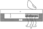
- the fingerprint identification device 02 includes at least one fingerprint sensing element 20 as shown in FIG. 3.
- the electronic device 01 also includes a fingerprint drive chip 21 electrically connected to each fingerprint sensing element 20.
- the fingerprint driving chip 21 and at least one fingerprint sensing element 20 may constitute the fingerprint identification module 200.
- the above-mentioned fingerprint drive chip 21 may be arranged on a PCB (hereinafter referred to as a motherboard) on the middle frame 11. Or, in some other embodiments of the present application, the aforementioned fingerprint drive chip 21 and the multiple fingerprint sensing elements 20 may be located in the same package. For the convenience of description, the following description is made by taking the fingerprint driving chip 21 on the motherboard of the electronic device 01 as an example.
- the user's fingerprint includes a plurality of raised ridges and sunken valleys.
- each fingerprint drive chip 21 can provide a drive signal to each fingerprint sensor element 20, and under the drive of the drive signal, the fingerprint sensor element 20 can respond to a small portion of the user’s finger corresponding to the position of the fingerprint sensor element 20. Fingerprints of some areas are collected. Then, the collected signal is transmitted to the processor on the motherboard by means of electrical signals.
- the processor can determine whether the user's fingerprint at the corresponding position of each fingerprint sensor element 20 is a ridge or valley line based on the above electrical signal, and can obtain the user's fingerprint by splicing the fingerprint information obtained by each fingerprint sensor element 20. So as to complete the collection or entry of user fingerprints. Next, the processor can also compare the fingerprints collected above with the fingerprints that have been entered to realize fingerprint identification.
- the aforementioned fingerprint sensing element 20 may be a photosensitive element capable of converting optical signals into electrical signals.
- the fingerprint identification device 02 also includes a light source.
- a light source that emits infrared light.
- the light source emits infrared light to the finger.
- the angle of refraction of the ridge line and valley line of the finger and the intensity of the light reflected to the fingerprint sensor element 20 are different, so that the fingerprint sensor element 20 corresponding to the ridge line position and the fingerprint sensor element 20 corresponding to the valley line position are different.
- the magnitude of the electrical signal generated by the sensing element 20 after photoelectric conversion is also different.
- each fingerprint sensing element 20 generates an electrical signal that matches the light signal reflected by the ridge or valley based on the intensity of the light reflected by the finger received.
- the aforementioned processor can determine the fingerprint information of the finger at the position where the fingerprint sensor 20 is located according to the electrical signal output by each fingerprint sensor 20.
- the fingerprint sensor element 20 is a photosensitive element capable of converting light signals into electrical signals
- the surface of the fingerprint sensor element 20 that receives light reflected by the finger is called the sensing surface of the fingerprint sensor element.
- the aforementioned fingerprint sensing element 20 may be an element capable of converting ultrasonic signals into electrical signals.
- the fingerprint identification device 02 also includes a signal generator for emitting ultrasonic waves. In this way, ultrasonic waves can be used to generate different echoes at the ridge and valley lines of the finger, so as to achieve the purpose of obtaining fingerprint information of the finger at the position where the fingerprint sensor 20 is located.
- the fingerprint sensing element 20 is an element capable of converting ultrasonic signals into electrical signals
- the side surface of the fingerprint sensing element 20 for receiving the ultrasonic echo reflected by the finger is called the sensing surface of the fingerprint sensing element.
- the fingerprint sensing element 20 may form an electric field with the electrolyte under the skin of the finger.
- the ridge line and valley line of the finger are respectively different from the electric field generated between the fingerprint sensor element 20, so as to achieve the purpose of obtaining fingerprint information of the finger at the position of the fingerprint sensor element 20.
- the fingerprint sensor element 20 uses the method of forming an electric field with the electrolyte under the finger's skin to perform fingerprint recognition, the fingerprint sensor element 20 is in the electronic device 01, close to the side surface of the finger, which is called the sensing surface of the fingerprint sensor element .
- the above is an example of the manner in which the fingerprint identification device 02 collects the user's fingerprint through the fingerprint sensor 20. The rest of the methods will not be repeated here.
- the present application does not limit the manner in which the fingerprint identification device 02 collects the user's fingerprint through the fingerprint sensing element 20, as long as the user's fingerprint can be collected to realize fingerprint identification.
- the aforementioned fingerprint identification device 02 can obtain the user's touch pressure before collecting the user's fingerprint, so as to determine whether the current user's touch operation is based on the magnitude of the touch pressure. Real touch operation is wrong touch.
- the fingerprint identification device 02 provided in the embodiment of the present application further includes a graphene pressure-sensitive layer 30 as shown in FIG. 4a.
- the aforementioned electronic device 01 also includes a pressure-sensitive driving chip 31 electrically connected to the graphene pressure-sensitive layer 30.
- the pressure-sensitive driving chip 31 and the graphene pressure-sensitive layer 30 can constitute a pressure sensing module 300.
- the pressure-sensitive driving chip 31 may be disposed on the main board on the middle frame 11. Or, in other embodiments of the present application, the pressure-sensitive driving chip 31 and the graphene pressure-sensitive layer 30 may also be located in the same package. For the convenience of description, the following descriptions are made by taking the pressure-sensitive driving chip 31 on the motherboard of the electronic device 01 as an example.
- the graphene pressure-sensitive layer 30 is deformed under the touch pressure applied by the user, so that the graphene pressure-sensitive layer 30 is deformed.
- the pressure-sensitive driving chip 31 is used to provide a driving signal to the graphene pressure-sensitive layer 30 electrically connected thereto.
- the impedance change caused by the graphene pressure-sensitive layer 30 when deformed can be used to obtain the touch pressure of the user.
- the pressure sensing module 300 with the graphene pressure sensing layer 30 adopts an impedance type pressure sensing method.
- the processor electrically connected to the graphene pressure-sensitive layer 30 can obtain the touch pressure of the user according to the change in the impedance of the graphene pressure-sensitive layer 30.
- the processor electrically connected to the graphene pressure-sensitive layer 30 can obtain the touch pressure of the user according to the change of the electrical signal output by the circuit having the graphene pressure-sensitive layer 30.
- the graphene pressure-sensitive layer 30 can be used as one electrode of the pressure-sensing capacitor, so that the graphene pressure-sensitive layer 30 can interact with the other electrode of the pressure-sensing capacitor when the graphene pressure-sensitive layer 30 is deformed.
- the pressure sensing module 300 with the graphene pressure sensing layer 30 adopts a capacitive pressure sensing method.
- the processor can obtain the touch pressure of the user according to the change of the capacitance value of the pressure sensing capacitor.
- the embodiment of the present application does not limit the pattern of the graphene pressure-sensitive layer 30, for example, it may be a block as shown in FIG. 4a. It can also be in the shape of a broken line as shown in Figure 4b. Those skilled in the art can set the pattern of the graphene pressure-sensitive layer 30 as needed.
- the pressure sensing module 300 adopts the resistive pressure sensing method, before the user performs a touch operation, compared to the block-shaped graphene pressure-sensitive layer 30, the broken line graphene pressure-sensitive The line width of the layer 30 is thinner and the length is larger, so the initial impedance is larger.
- the pressure sensing module 300 adopts the capacitive pressure sensing method
- the distance between the two electrodes in the pressure sensing capacitor remains unchanged, before the user performs a touch operation
- the relative For the graphene pressure-sensitive layer 30 in the shape of a broken line, the block-shaped graphene pressure-sensitive layer 30 has a relatively large area between one electrode of the pressure-sensing capacitor and the other electrode of the pressure-sensing capacitor.
- the initial capacitance of the capacitor is relatively large.
- the method for manufacturing the graphene pressure-sensitive layer 30 may be as follows: after the graphene piezoresistive paste and the metallic silver paste are mixed, the printing process is used to mix the composite material according to a preset pattern. The paste is printed on a flexible film substrate. After drying and curing, the graphene pressure-sensitive layer 30 is formed.
- the method for manufacturing the graphene pressure-sensitive layer 30 may be to grow a single layer on a metal foil, such as copper foil, by chemical vapor deposition (CVD) or the like. Or multilayer graphene film. Then, the single-layer or multi-layer graphene film and the copper foil are peeled off by solution etching to form the graphene pressure-sensitive layer 30. Next, the peeled graphene pressure-sensitive layer 30 is transferred to the flexible film substrate.
- CVD chemical vapor deposition
- the above-mentioned flexible film substrate may be polyimide film (PI), polyethylene terephthalate (PET), polymethyl methacrylate (polymethyl methacrylate, PMMA) and other membrane materials.
- PI polyimide film
- PET polyethylene terephthalate
- PMMA polymethyl methacrylate
- the fingerprint identification device 02 is located on the back of the display module 10.
- the fingerprint identification device 02 is pasted on the back of the display module 10 (the side surface facing the middle frame 11) through glue, such as optically clear adhesive (OCA).
- OCA optically clear adhesive
- the sensor surface of the fingerprint sensor 20 faces the back of the display module 10. The description of the sensing surface of the fingerprint sensing element 20 is the same as that described above, and will not be repeated here.
- all fingerprint sensing elements 20 in the fingerprint identification device 02 are integrated with the graphene pressure-sensitive layer 30.
- the integration method of the fingerprint sensor 20 and the graphene pressure-sensitive layer 30 will be described as an example below.
- the aforementioned graphene pressure-sensitive layer 30 may be located on the side where the sensing surfaces of the multiple fingerprint sensing elements 20 are located.
- the fingerprint identification module 200 further includes a covering layer 22 covering the sensing surface of each fingerprint sensing element 20, and a substrate 23 for carrying each fingerprint sensing element 20.
- the above-mentioned cover layer 22 may be an encapsulation layer for encapsulating a plurality of fingerprint sensing elements 20.
- the substrate 23 may be a circuit board provided with a circuit structure.
- the circuit board can be a PCB or an FPC.
- a plurality of fingerprint sensing elements 20 may be fabricated on the substrate 23, and the sensing surfaces of the plurality of fingerprint sensing elements 20 may be covered with the covering layer 22 to form the fingerprint identification module 200. Then, the above-mentioned graphene pressure-sensitive layer 30 is fabricated on the surface of the cover layer 22 of the fingerprint identification module 200 away from the fingerprint sensor element 20, so that the graphene pressure-sensitive layer 30 is located on the cover layer 22 away from the fingerprint sensor element 20 surface.
- the graphene pressure-sensitive layer 30 can be fabricated on the surface of the covering layer 22 away from the fingerprint sensor 20 by printing.
- the graphene pressure-sensitive layer 30 formed by peeling off the single-layer or multi-layer graphene film grown on the copper foil is directly transferred to the surface of the covering layer 22 away from the fingerprint sensing element 20.
- the fingerprint identification module 200 can be integrated with the graphene pressure-sensitive layer 30.
- the manufacturing process of the graphene pressure-sensitive layer 30 is the same as described above, and will not be repeated here.
- the flexible film substrate on which the graphene pressure-sensitive layer 30 is formed can also be attached to the surface of the cover layer 22 away from the fingerprint sensor 20. In this way, the fingerprint sensing element 20 and the graphene pressure-sensitive layer 30 can be integrated.
- the side where the graphene pressure-sensitive layer 30 is located in the fingerprint identification device 02 can be connected to the display module 10 through a colloid.
- the back side is glued together.
- the fingerprint identification device 02 adopts an optical fingerprint identification method, in order to enable more light reflected by the finger to enter the fingerprint sensing element 20.
- the material constituting the above-mentioned covering layer 22 and the material of the flexible film substrate for supporting the graphene pressure-sensitive layer 30 can be selected from resin materials with higher light transmittance.
- the vertical projection of all fingerprint sensing elements 20 in the fingerprint identification device 02 on the display module 10 is within the range of the vertical projection of the graphene pressure-sensitive layer 30 on the display module 10.
- the graphene pressure-sensitive layer 30 can cover all fingerprint sensing elements 20, so that the graphene pressure-sensitive layer 30 can cover any position in the touch fingerprint identification device 02 that can identify fingerprints, thereby effectively reducing fingerprint identification.
- the area of the pressure detection blind zone of the device 02 improves the accuracy of the fingerprint recognition device 02 to detect touch pressure.
- the graphene pressure-sensitive layer 30 may be located on the sensing surfaces of multiple fingerprint sensing elements 20, in other embodiments of the present application, as shown in FIG. 7, the graphene pressure-sensitive layer 30 may be located on the fingerprint sensor. Between the sensing element 20 and the covering layer 22. In this way, the fingerprint identification module 200 can be integrated with the graphene pressure-sensitive layer 30.
- the manufacturing process of the graphene pressure-sensitive layer 30 is the same as described above, and will not be repeated here.
- the touch pressure will be applied to the display module 10
- the touch pressure can cause the display module 10 to deform, thereby driving the graphene pressure-sensitive layer 30 connected to it to deform.
- the pressure-sensitive driving chip 31 sends a driving signal to the graphene pressure-sensitive layer 30, when the graphene pressure-sensitive layer 30 is deformed, its impedance changes.
- the electronic device 01 having the fingerprint sensing element 20 further includes a processor 100 as shown in FIG. 8.
- the processor 100 can be arranged on a motherboard (PCB shown in FIG. 1b). Based on this, the processor 100 shown in FIG. 8 in the pressure sensing module 300 can compare the impedance value of the graphene pressure-sensitive layer 30 after deformation with the impedance value before deformation, thereby confirming the user according to the comparison result. The touch pressure applied. Or, in other embodiments of the present application, the processor 100 shown in FIG. 8 in the pressure sensing module 300 provides the electrical signal to the processor 100 according to the graphene pressure-sensitive layer 30 after the deformation, and the electrical signal before the deformation The voltage is compared to confirm the touch pressure applied by the user according to the comparison result.
- the processor 100 After the processor 100 obtains the aforementioned touch pressure, it can be compared with a preset pressure threshold, such as 1N. When the aforementioned touch pressure is greater than the pressure threshold, it can indicate that the user is performing a real touch operation.
- a preset pressure threshold such as 1N.
- the processor 100 may send the first instruction to the fingerprint driving chip 21.
- the fingerprint drive chip 21 drives each fingerprint sensing element 20 electrically connected to the fingerprint drive chip 21 to collect the user's fingerprint.
- the collected fingerprints can be transmitted to the fingerprint identification module 200, and the collected fingerprints can be matched with the fingerprints entered in advance through the fingerprint identification module 200 to realize fingerprint identification.
- the processor 100 when the processor 100 obtains that the touch pressure is less than the pressure threshold, it may indicate that the touch operation performed by the user is a wrong touch.
- the processor 100 may send a second instruction to the fingerprint driving chip 21.
- the fingerprint driving chip 21 stops providing driving signals to the fingerprint sensing elements 20 electrically connected to the fingerprint driving chip 21. Therefore, the fingerprint identification device 02 will not collect the user's fingerprint when the user touches by mistake.
- the material constituting the graphene pressure-sensitive layer 30 mainly includes graphene.
- the thickness of the single-layer graphene film in the graphene pressure-sensitive layer 30 can be made very thin, for example, about 0.34 nm. Therefore, after the graphene pressure-sensitive layer 30 is integrated with a plurality of fingerprint sensing elements 20, the size of the fingerprint identification device 02 can be reduced. The requirement of the fingerprint identification device 02 on the space structure of the electronic device 01 is reduced.
- the pressure sensing module 300 with the graphene pressure-sensitive layer 30 has higher sensitivity.
- the touch pressure changes within 0 ⁇ 500 g, there is still a linear relationship between the electrical signal sent by the graphene pressure-sensitive layer 30 to the processor 100 and the touch pressure applied by the user.
- the graphene pressure-sensitive layer 30 has a very high strength, which can be more than 100 times the strength of steel, so as to reduce the probability that the graphene pressure-sensitive layer 30 will break when a user uses an electronic device.
- the graphene pressure-sensitive layer 30 includes a plurality of sensing sub-blocks 301 arranged at intervals. Each sensing sub-block 301 corresponds to at least one fingerprint sensing element 20.
- sensing sub-blocks 301 can be connected in parallel, and each sensing sub-block 301 is separately electrically connected to the fingerprint drive chip 21 and the processor 100 as shown in FIG. 8. In this way, on the one hand, since the plurality of sensing sub-blocks 301 are not connected to each other, the probability of mutual interference of the touch pressure on each sensing sub-block 301 is reduced, and the sensing of each sensing sub-block 301 is improved. The accuracy of the user's touch pressure.
- the processor 100 in FIG. 8 can also obtain the actual touch area of the user according to the number of sensing sub-blocks 301 whose impedance values change each time the user touches. Then, the actual touch area is compared with a preset area threshold, and when the actual touch area is less than the area threshold, it can be determined that the user's touch operation is a wrong touch. At this time, the processor 100 can control the fingerprint driving chip 21 to stop providing driving signals to the fingerprint sensing elements 20 electrically connected to the fingerprint driving chip 21.
- the sensing sub-blocks 301 are connected in parallel, the data collected by them are independent of each other. Therefore, according to the position of the sensing sub-block 301 and the touch pressure it receives, the changing trend of the finger force during the user's touch can be obtained, so that the pressing direction, speed and pressing type of the finger can be obtained.
- the processor 100 connected to each of the above-mentioned sensing sub-blocks 301 can determine the user's touch direction according to the sequence of changes in the impedance values of each of the above-mentioned sensing sub-blocks 301, thereby determining the user
- the touch method is swipe from left to right.
- the electronic device can perform an operation corresponding to the touch mode according to the determined touch mode. For example, the page turning action performed when reading an e-book.
- the graphene pressure-sensitive layer 30 in the fingerprint identification device 02 is integrated with the fingerprint identification module 200 mainly composed of multiple fingerprint sensing elements 20.
- the electronic device 01 includes a housing assembly 03 as shown in FIG. 10a.
- the housing assembly 03 includes a middle frame 11.
- the middle frame 11 includes a carrying board 110 for carrying a circuit board, and a frame 111 arranged around the carrying board 110.
- the frame 111 is provided with a button hole 112.
- the key hole 112 is a through hole.
- the housing assembly 03 also includes the aforementioned fingerprint identification device 02.
- the fingerprint identification device 02 can be used as a key set in the key hole 112 and connected to the frame 111.
- the sensing surface of the fingerprint sensing element 20 in the fingerprint identification device 02 faces the outer surface of the frame 111, so that the user's fingerprint can be identified.
- the following describes how the fingerprint identification device 02 is arranged in the key hole 112 of the frame 111 in combination with the integration manner of the graphene pressure-sensitive layer 30 and the fingerprint identification module 200 in the fingerprint identification device 02.
- the graphene pressure-sensitive layer 30 may be located on the sensing surface of the multiple fingerprint sensing elements 20.
- the fingerprint identification module 200 further includes a covering layer 22 covering the sensing surface of each fingerprint sensing element 20 and carrying each In the case of the substrate 23 of the fingerprint sensor 20, the graphene pressure-sensitive layer 30 can be fabricated on the surface of the cover layer 22 away from the fingerprint sensor 20.
- the sensing surface of the fingerprint sensing element 20 faces the covering layer 22. Therefore, the graphene pressure-sensitive layer 30 faces the outer side of the frame 111 relative to the fingerprint recognition module 200, thereby being closer to the user's finger.
- the fingerprint identification module 200 and the key hole 112 can be bonded by an adhesive layer, or by arranging engagement components such as protrusions and grooves on the mating surface of the fingerprint identification module 200 and the key hole 112, the fingerprint identification device 02 The frames 111 are connected.
- the graphene pressure-sensitive layer 30 is disposed between the fingerprint sensor 20 and the cover layer 22. At this time, the graphene pressure-sensitive layer 30 is integrated in the fingerprint identification module 200. As described above, in order to expose the sensing surface of each fingerprint sensing element 20 in the fingerprint recognition module 200 for fingerprint recognition, the graphene pressure-sensitive layer 30 faces the outside of the frame 111 relative to the fingerprint recognition module 200 and is closer to the user's finger.
- the graphene pressure-sensitive layer 30 is located on the side of the fingerprint sensing element 20 away from its sensing surface.
- the sensing surface of the fingerprint sensing element 20 faces the covering layer 22.
- the graphene pressure-sensitive layer 30 is located on the surface of the substrate 23 away from the fingerprint sensor 20.
- the graphene pressure-sensitive layer 30 faces the inner side of the frame 111 relative to the fingerprint recognition module 200. Keep away from the user's fingers.
- the graphene pressure-sensitive layer 30 is located between the substrate 23 and the fingerprint sensor 20. As described above, in order to expose the sensing surface of each fingerprint sensing element 20 in the fingerprint recognition module 200 to achieve fingerprint recognition, the graphene pressure-sensitive layer 30 faces the inner side of the frame 111 relative to the fingerprint recognition module 200.
- the graphene pressure-sensitive layer 30 includes a plurality of sensing sub-blocks 301 arranged at intervals (as shown in FIG. 9) , I won’t repeat it here.
- the fingerprint identification device 02 can be used as a button to be arranged in the button hole 112 opened on the frame 111.
- the graphene pressure-sensitive layer 30 includes a plurality of sensing sub-blocks 301 arranged at intervals, the user can press differently The way of fingerprint identification device 02 enables different key operations.
- the processor 100 connected to each of the above-mentioned sensing sub-blocks 301 can determine that the user presses according to the position of the sensing sub-block 301 whose impedance changes The position is at the top of the button.
- the upper end of the button can correspond to the volume increase function, so that the volume can be increased when the electronic device is playing audio.
- the processor 100 connected to each of the above-mentioned sensing sub-blocks 301 can change the sensor according to the impedance value.
- the position of block 301 determines that the position pressed by the user is located at the lower end of the key.
- the lower end of the button can correspond to the volume reduction function, so that the volume can be reduced when the electronic device is playing audio.
- the processor 100 may also determine that the user's touch operation is an upward sliding based on the impedance changes from bottom to top in the plurality of sensing sub-blocks 301 in turn. Conversely, when the plurality of sensing sub-blocks 301 sequentially move from top to bottom impedance When a change occurs, the processor 100 determines that the user's touch operation is sliding down. Thus, the electronic device 01 can perform operations that match different sliding directions.
- the electronic device 01 has a fingerprint recognition area 04 as shown in FIG. 11a.
- the user can put his finger in the fingerprint recognition area 04.
- the electronic device 01 also includes a fingerprint identification device 02 and a display module 10 as shown in FIG. 11b.
- the structure of the display module 10 is as described above, and will not be repeated here.
- the fingerprint identification device 02 includes a graphene pressure sensitive layer 30 located in the fingerprint identification area 04 and at least one fingerprint sensing element 20.
- the fingerprint sensing element 20 is used to collect the user's fingerprint, and the sensing surface of the fingerprint sensing element 20 faces the back B of the display module 10 (as shown in FIG. 1b, the display module 10 faces the side surface of the middle frame 11).
- the above electronic device 01 also includes a pressure-sensitive driving chip 31 (shown in FIG. 8) electrically connected to the graphene pressure-sensitive layer 30.
- the function and setting method of the pressure-sensitive driving chip 31 are the same as described above, and will not be repeated here.
- each fingerprint sensing element 20 is connected to the back of the display module 10, and as shown in FIG. 11c, the graphene pressure-sensitive layer 30 is disposed around all the fingerprint sensing elements 20.
- the graphene pressure-sensitive layer 30 is a closed frame structure. All the fingerprint sensing elements 20 are located in the hollow area of the frame structure, so that the graphene pressure-sensitive layer 30 is arranged around the fingerprint identification module 200 with the fingerprint sensing elements 20.
- the manufacturing method of the graphene pressure-sensitive layer 30 is the same as that described above, and will not be repeated here.
- the graphene pressure-sensitive layer 30 includes a plurality of sensing sub-blocks 301 arranged at intervals (as shown in FIG. 9). I won't repeat it here.
- the electronic device 01 has a fingerprint recognition area 04.
- the electronic device 01 also includes a display module 10 and a fingerprint identification device 02.
- the fingerprint identification device 02 includes a graphene pressure sensitive layer 30 located in the fingerprint identification area 04 and at least one fingerprint sensing element 20.
- the fingerprint sensor 20 is used to collect a user's fingerprint, and the sensor surface of the fingerprint sensor 20 faces the back of the display module 10.
- the difference from Example 3 is that the electronic device 01 also includes a middle frame 11 as shown in FIG. 12.
- the middle frame 11 includes a carrier board 110 for carrying a circuit board, and a frame 111 arranged around the carrier board 110.
- the graphene pressure-sensitive layer 30 is connected to the back of the display module 10.
- the display module 10 is connected to the frame 111, and there is a first gap H1 between the back surface B of the display module 10 and the supporting board 110.
- Each fingerprint sensing element 20 is connected to a side surface of the supporting board 110 facing the display module 10, and the fingerprint sensing element 20 is located on the supporting board 110 with a second gap H2 between the fingerprint sensing element 20 and the graphene pressure-sensitive layer 30.
- the fingerprint sensing element 20 By disposing the fingerprint sensing element 20 on the carrier plate 110 and having a second gap H2 between the fingerprint sensing element 20 and the graphene pressure-sensitive layer 30, the distance between the user's finger and the fingerprint sensing element 20 can be increased. Therefore, when the fingerprint sensing element 20 is a photoelectric conversion element, the fingerprint sensing element 20 is advantageous for distinguishing the reflection of the ridge line of the finger and the reflection of the valley line.
- the electronic device 01 also includes a pressure-sensitive driving chip 31 electrically connected to the graphene pressure-sensitive layer 30.
- a pressure-sensitive driving chip 31 electrically connected to the graphene pressure-sensitive layer 30.
- the graphene pressure-sensitive layer 30 deforms, and the resistance of the graphene pressure-sensitive layer 30 is reduced. Changes. In this way, the touch pressure of the user is obtained according to the amount of change in the impedance of the graphene pressure-sensitive layer 30.
- the graphene pressure-sensitive layer 30 may form a pressure-sensing capacitor with the carrier plate 110. Driven by the driving signal provided by the pressure-sensitive driving chip 31, when the user performs fingerprint recognition, the graphene pressure-sensitive layer 30 is deformed and the capacitance value of the pressure-sensing capacitor changes. In this way, the touch pressure of the user is obtained according to the amount of change in the capacitance value of the sensing capacitor.
- the vertical projection of all fingerprint sensing elements 20 in the fingerprint identification device 02 on the display module 10 is within the range of the vertical projection of the graphene pressure-sensitive layer 30 on the display module 10.
- the graphene pressure-sensitive layer 30 can cover all the fingerprint sensing elements 20, so that the graphene pressure-sensitive layer 30 can cover any position where the fingerprint identification device 02 can recognize fingerprints, thereby effectively reducing fingerprints
- the area of the pressure detection blind area of the identification device 02 improves the accuracy of the fingerprint identification device 02 in detecting touch pressure.
- the manufacturing method of the graphene pressure-sensitive layer 30 is the same as that described above, and will not be repeated here.
- the graphene pressure-sensitive layer 30 includes a plurality of sensing sub-blocks 301 arranged at intervals (as shown in FIG. 9). I won't repeat it here.
Landscapes
- Engineering & Computer Science (AREA)
- Theoretical Computer Science (AREA)
- General Engineering & Computer Science (AREA)
- Physics & Mathematics (AREA)
- General Physics & Mathematics (AREA)
- Human Computer Interaction (AREA)
- Computer Security & Cryptography (AREA)
- Computer Hardware Design (AREA)
- Software Systems (AREA)
- Multimedia (AREA)
- Image Input (AREA)
- Measurement Of The Respiration, Hearing Ability, Form, And Blood Characteristics Of Living Organisms (AREA)
Abstract
A fingerprint recognition device (02) and an electronic apparatus (01), relating to the field of fingerprint recognition. The fingerprint recognition device (02) comprises at least one fingerprint sensing element (20) and a graphene pressure-sensing layer (30). The fingerprint sensing element (20) is used to acquire a fingerprint of a user. The graphene pressure-sensing layer (30) is located on a side of the fingerprint sensing element (20) provided with a sensing surface, or located on a side of the fingerprint sensing element (20) facing away from the sensing surface of the fingerprint sensing element (20). The graphene pressure-sensing layer (30) deforms as a result of the touch pressure applied by the user. The invention can reduce the probability of ghost-touching when the electronic apparatus (01) is being used by a user.
Description
本申请要求在2019年5月22日提交中国国家知识产权局、申请号为201910431503.7的中国专利申请的优先权,发明名称为“一种指纹识别装置、电子设备”的中国专利申请的优先权,其全部内容通过引用结合在本申请中。This application claims the priority of a Chinese patent application filed with the State Intellectual Property Office of China with application number 201910431503.7, and the priority of a Chinese patent application with the title of "a fingerprint identification device, electronic equipment" on May 22, 2019. The entire content is incorporated into this application by reference.
本申请涉及指纹识别领域,尤其涉及一种指纹识别装置、电子设备。This application relates to the field of fingerprint identification, and in particular to a fingerprint identification device and electronic equipment.
随着生物识别技术的发展,指纹识别技术因其具有安全性好,可靠性高,使用简单方便等特点,使得指纹识别技术被广泛应用于保护个人信息安全的各种领域,尤其是电子设备领域,例如手机、笔记本电脑、平板的电脑、数码相机等。然而,用户在使用上述电子设备的过程中,当手指无意接触到电子设备中的指纹识别位置时,容易发生误触控,导致电子设备误解锁的现象发生,从而降低了用户体验。With the development of biometric technology, fingerprint recognition technology has the characteristics of good security, high reliability, simple and convenient use, etc., making fingerprint recognition technology widely used in various fields to protect personal information security, especially in the field of electronic equipment , Such as mobile phones, laptops, tablet computers, digital cameras, etc. However, in the process of using the above electronic device, when a finger accidentally touches the fingerprint recognition position in the electronic device, a false touch is prone to occur, causing the electronic device to be unlocked by mistake, thereby reducing the user experience.
发明内容Summary of the invention
本申请实施例提供一种指纹识别装置、电子设备,可以减小用户使用电子设备的过程中,发生指纹误触控现象的几率。The embodiments of the present application provide a fingerprint identification device and an electronic device, which can reduce the probability of a fingerprint false touch phenomenon when a user uses the electronic device.
为达到上述目的,本申请实施例采用如下技术方案:In order to achieve the foregoing objectives, the following technical solutions are adopted in the embodiments of this application:
本申请实施例的第一方面,提供一种指纹识别装置。该指纹识别装置包括至少一个指纹感应元件和石墨烯压感层。该指纹感应元件用于采集用户的指纹。石墨烯压感层位于指纹感应元件的感应面所在的一侧。或者,石墨烯压感层可以位于指纹感应元件远离其感应面的一侧。石墨烯压感层用于在用户施加的触控压力的作用下发生形变。当用户使用具有上述指纹识别装置的电子设备的过程中,手指触控到指纹识别装置时,会对显示模组施加触控压力,该触控压力能够使得显示模组发生形变,从而带动与其相连接的石墨烯压感层发生形变。石墨烯压感层变形时,其阻抗发生变化。在此情况下,可以根据石墨烯压感层在变形后的阻抗值与变形前的阻抗值进行比对,从而获得用户施加的触控压力。或者,在本申请的另一些实施例中,根据石墨烯压感层在变形后向处理器提供的电信号,与变形前的电压进行比对,从而获得用户施加的触控压力。基于此,当获得上述触控压力后,可以与预先设置的压力阈值进行比对。当上述触控压力大于压力阈值时,可以说明用户执行的是真实的触控操作。在此情况下,各个指纹感应元件可以对用户的指纹进行采集。采集后的指纹可以与预先录入的指纹进行匹配,以实现指纹识别。或者,当获得的触控压力小于压力阈值时,可以说明用户执行的触控操作为误触控。在此情况下,各个指纹感应元件不会对用户的指纹进行采集,防止误触控的现象发生。此外,构成石墨烯压感层的材料主要包括石墨烯。该石墨烯压感层中单层的石墨烯薄膜的厚度可以制作的很薄。从而在将该石墨烯压感层与多个指纹感应元件集成后,可以有利于减小指纹识别装置的尺寸。降低了指纹识别装置对电子设备中空间架构的要求。此外,石墨烯压感层在受力变形后,其阻抗可以发生灵敏的可恢复线性变化。从而使得具有该石墨烯压感层的压力感测模块具有较高的灵敏度。当触控压力在0~500g内变化时,石墨烯压感层发送的电信号与用户施加的触控压力之间仍然存在线性关系。再者,石墨烯压感层具有很高的强度,可以是钢铁强度的100多倍,从而能够减小用户在使用电子设备的过程中,发生石墨烯压感层断裂的几率。The first aspect of the embodiments of the present application provides a fingerprint identification device. The fingerprint identification device includes at least one fingerprint sensing element and a graphene pressure-sensitive layer. The fingerprint sensor is used to collect the user's fingerprint. The graphene pressure-sensitive layer is located on the side where the sensing surface of the fingerprint sensing element is located. Alternatively, the graphene pressure-sensitive layer may be located on the side of the fingerprint sensing element away from its sensing surface. The graphene pressure-sensitive layer is used to deform under the touch pressure applied by the user. When the user uses the electronic device with the above-mentioned fingerprint recognition device, when the finger touches the fingerprint recognition device, touch pressure is applied to the display module. The touch pressure can cause the display module to deform and drive the corresponding The connected graphene pressure-sensitive layer is deformed. When the graphene pressure-sensitive layer deforms, its impedance changes. In this case, the impedance value of the graphene pressure-sensitive layer after deformation can be compared with the impedance value before deformation, so as to obtain the touch pressure applied by the user. Or, in some other embodiments of the present application, the electrical signal provided by the graphene pressure-sensitive layer to the processor after the deformation is compared with the voltage before the deformation, so as to obtain the touch pressure applied by the user. Based on this, when the aforementioned touch pressure is obtained, it can be compared with a preset pressure threshold. When the aforementioned touch pressure is greater than the pressure threshold, it can indicate that the user is performing a real touch operation. In this case, each fingerprint sensing element can collect the user's fingerprint. The collected fingerprints can be matched with pre-entered fingerprints to realize fingerprint identification. Or, when the obtained touch pressure is less than the pressure threshold, it may indicate that the touch operation performed by the user is a wrong touch. In this case, each fingerprint sensor element will not collect the user's fingerprint to prevent false touch. In addition, the material constituting the graphene pressure-sensitive layer mainly includes graphene. The thickness of the single-layer graphene film in the graphene pressure-sensitive layer can be made very thin. Therefore, after the graphene pressure-sensitive layer is integrated with multiple fingerprint sensing elements, the size of the fingerprint identification device can be reduced. The fingerprint identification device's requirements for the spatial structure of the electronic equipment are reduced. In addition, after the graphene pressure-sensitive layer is deformed by force, its impedance can undergo a sensitive and recoverable linear change. Thus, the pressure sensing module with the graphene pressure sensing layer has higher sensitivity. When the touch pressure changes within 0˜500 g, there is still a linear relationship between the electrical signal sent by the graphene pressure-sensitive layer and the touch pressure applied by the user. Furthermore, the graphene pressure-sensitive layer has a very high strength, which can be more than 100 times the strength of steel, so as to reduce the probability that the graphene pressure-sensitive layer will break when users use electronic devices.
可选的,石墨烯压感层包括多个间隔设置的感应子块。每个感应子块对应至少一个指纹感应元件。这样一来,一方面,由于上述多个感应子块彼此没有相连接,因此减小了各个感应子块受到的触控压力发生相互干扰的几率,提高了每个感应子块感测用户触控压力的精度。又一方面,还可以根据每次用户触控时,阻抗值发生变化的感应子块的个数,获得用户的实际触控面积。然后,将该实际触控面积与预先设置的面积阈值进行比对,当实际触控面积小于面积阈值时,可以判断出上述用户的触控操作为误触控。Optionally, the graphene pressure-sensitive layer includes a plurality of sensing sub-blocks arranged at intervals. Each sensing sub-block corresponds to at least one fingerprint sensing element. In this way, on the one hand, since the above-mentioned multiple sensing sub-blocks are not connected to each other, the probability of mutual interference of the touch pressure on each sensing sub-block is reduced, and each sensing sub-block is increased to sense the user's touch. The accuracy of the pressure. In another aspect, the actual touch area of the user can be obtained according to the number of sensing sub-blocks whose impedance values change each time the user touches. Then, the actual touch area is compared with a preset area threshold, and when the actual touch area is less than the area threshold, it can be determined that the user's touch operation is a wrong touch.
可选的,指纹识别装置还包括覆盖指纹感应元件的感应面的覆盖层。石墨烯压感层位于覆盖层远离指纹感应元件的一侧表面。或者,石墨烯压感层位于指纹感应元件与覆盖层之间。从而可以实现指纹识别模块与石墨烯压感层的集成。Optionally, the fingerprint identification device further includes a covering layer covering the sensing surface of the fingerprint sensing element. The graphene pressure-sensitive layer is located on the side surface of the cover layer away from the fingerprint sensing element. Alternatively, the graphene pressure-sensitive layer is located between the fingerprint sensing element and the cover layer. Thus, the integration of the fingerprint recognition module and the graphene pressure-sensitive layer can be realized.
可选的,指纹识别装置还包括用于承载每个指纹感应元件的衬底。石墨烯压感层位于衬底远离指纹感应元件的一侧表面。或者,石墨烯压感层位于衬底与指纹感应元件之间。从而可以实现指纹识别模块与石墨烯压感层的集成。Optionally, the fingerprint identification device further includes a substrate for carrying each fingerprint sensing element. The graphene pressure sensitive layer is located on the side surface of the substrate away from the fingerprint sensing element. Alternatively, the graphene pressure-sensitive layer is located between the substrate and the fingerprint sensing element. Thus, the integration of the fingerprint recognition module and the graphene pressure-sensitive layer can be realized.
本申请实施例的第二方面,提供一种电子设备。该电子设备包括显示模组以及如上所述的任意一种指纹识别装置。显示模组包括显示面和远离显示面的背面。指纹识别装置位于显示模组的背面,且指纹识别装置中指纹感应元件的感应面朝向显示模组的背面。该电子设备具有与前述实施例提供的指纹识别装置相同的技术效果,此处不再赘述。The second aspect of the embodiments of the present application provides an electronic device. The electronic equipment includes a display module and any fingerprint identification device as described above. The display module includes a display surface and a back surface away from the display surface. The fingerprint identification device is located on the back of the display module, and the sensing surface of the fingerprint sensor element in the fingerprint identification device faces the back of the display module. This electronic device has the same technical effect as the fingerprint identification device provided in the foregoing embodiment, and will not be repeated here.
可选的,指纹识别装置中所有指纹感应元件在显示模组上的垂直投影,位于石墨烯压感层在显示模组上的垂直投影的范围内。这样一来,石墨烯压感层可以将各个指纹感应元件均覆盖,使得石墨烯压感层可以覆盖触摸指纹识别装置中任意一个能够识别指纹的位置,从而可以有效减小指纹识别装置的压力检测盲区的面积,提升指纹识别装置检测触控压力的精度。Optionally, the vertical projection of all fingerprint sensing elements in the fingerprint identification device on the display module is within the range of the vertical projection of the graphene pressure-sensitive layer on the display module. In this way, the graphene pressure-sensitive layer can cover each fingerprint sensing element, so that the graphene pressure-sensitive layer can cover any position in the fingerprint recognition device that can recognize fingerprints, thereby effectively reducing the pressure detection of the fingerprint recognition device The area of the blind zone improves the accuracy of the fingerprint recognition device in detecting touch pressure.
可选的,电子设备还包括压感驱动芯片。压感驱动芯片与石墨烯压感层电连接,用于向各个指纹感应元件提供驱动信号。上述指纹驱动芯片可以设置于主板上。或者,在本申请的另一些实施例中,上述指纹驱动芯片可以与多个指纹感应元件位于同一个封装体内。Optionally, the electronic device further includes a pressure-sensitive driving chip. The pressure-sensitive driving chip is electrically connected to the graphene pressure-sensitive layer, and is used to provide driving signals to each fingerprint sensing element. The above-mentioned fingerprint drive chip can be arranged on the motherboard. Or, in some other embodiments of the present application, the above-mentioned fingerprint driving chip and multiple fingerprint sensing elements may be located in the same package.
本申请实施例的第三方面,提供一种壳体组件。该壳体组件包括中框以及如上所述的任意一种指纹识别装置。其中,中框包括用于承载电路板的承载板,以及绕承载板一周设置的边框。该边框上设置有按键孔。指纹识别装置位于按键孔内,且与边框相连接。指纹识别装置中的指纹感应元件的感应面朝向边框的外表面,从而能够对用户的指纹进行识别。指纹感应元件和石墨烯压感层与电路板电连接。该壳体组件具有与前述实施例提供的指纹识别装置相同的技术效果,此处不再赘述。A third aspect of the embodiments of the present application provides a housing assembly. The housing assembly includes a middle frame and any fingerprint identification device as described above. Wherein, the middle frame includes a carrying board for carrying the circuit board and a frame arranged around the carrying board. Button holes are provided on the frame. The fingerprint identification device is located in the button hole and connected to the frame. The sensing surface of the fingerprint sensing element in the fingerprint identification device faces the outer surface of the frame, so that the user's fingerprint can be identified. The fingerprint sensing element and the graphene pressure sensing layer are electrically connected to the circuit board. The housing assembly has the same technical effect as the fingerprint identification device provided in the foregoing embodiment, and will not be repeated here.
本申请实施例的第四方面,提供一种电子设备。该电子设备包括显示模组以及如上所述的壳体组件。显示模组位于中框中,承载板远离电路板的一侧表面,且显示模组与中框相连接。该电子设备具有与前述实施例提供的壳体组件相同的技术效果,此处不再赘述。The fourth aspect of the embodiments of the present application provides an electronic device. The electronic device includes a display module and the aforementioned housing assembly. The display module is located in the middle frame, the carrying board is away from the side surface of the circuit board, and the display module is connected with the middle frame. The electronic device has the same technical effect as the housing assembly provided in the foregoing embodiment, and will not be repeated here.
本申请实施例的第四方面,提供一种电子设备。该电子设备包括指纹识别区、显示模组和指纹识别装置。显示模组包括显示面和远离显示面的背面。指纹识别装置包括位于指纹识别区的石墨烯压感层和至少一个指纹感应元件。该指纹感应元件用于采集用户的指纹,且指纹感应元件的感应面朝向显示模组的背面。石墨烯压感层与显示模组的背面相连接,且用于在用户施加的触控压力的作用下发生形变。上述电子设备具有与前述实施例提供的指纹识别装置相同的技术效果,此处不再赘述。The fourth aspect of the embodiments of the present application provides an electronic device. The electronic equipment includes a fingerprint identification area, a display module and a fingerprint identification device. The display module includes a display surface and a back surface away from the display surface. The fingerprint identification device includes a graphene pressure-sensitive layer located in a fingerprint identification area and at least one fingerprint sensing element. The fingerprint sensing element is used to collect the user's fingerprint, and the sensing surface of the fingerprint sensing element faces the back of the display module. The graphene pressure-sensitive layer is connected to the back of the display module, and is used to deform under the touch pressure applied by the user. The above-mentioned electronic device has the same technical effect as the fingerprint identification device provided in the foregoing embodiment, and will not be repeated here.
可选的,每个指纹感应元件与显示模组的背面相连接。石墨烯压感层位于指纹感应元件的周边。从而可以使得用户在通过指纹感应元件进行指纹识别时,位于该指纹感应元件周边的石墨烯压感层可以对用户的触控压力进行采集。Optionally, each fingerprint sensing element is connected to the back of the display module. The graphene pressure-sensitive layer is located on the periphery of the fingerprint sensor. Therefore, when the user performs fingerprint recognition through the fingerprint sensor element, the graphene pressure-sensitive layer located around the fingerprint sensor element can collect the user's touch pressure.
可选的,石墨烯压感层为闭合的框架结构。所有指纹感应元件位于该框架结构的中空区域内。从而当用户执行触控操作时,位于所有指纹感应元件周边的石墨烯压感层能够在按压位置处均匀的发生形变,从而使得获得的按压力度更加准确。Optionally, the graphene pressure-sensitive layer is a closed frame structure. All fingerprint sensing elements are located in the hollow area of the frame structure. Therefore, when the user performs a touch operation, the graphene pressure-sensitive layer located around all the fingerprint sensing elements can be uniformly deformed at the pressing position, so that the obtained pressing force is more accurate.
可选的,电子设备还包括中框。该中框包括承载板以及绕承载板一周设置的边框。显示模组的背面与边框相连接,且显示模组的背面与承载板之间具有第一间隙。每个指纹感应元件与承载板朝向显示模组的一侧表面相连接,且指纹感应元件与石墨烯压感层之间具有第二间隙。通过将指纹感应元件设置于承载板上,且与石墨烯压感层之间具有第二间隙,可以增加用户的手指与指纹感应元件之间的间距。从而在指纹感应元件为光电转换元件时,使得指纹感应元件有利于区分出手指脊线的反射和谷线反射光线。Optionally, the electronic device further includes a middle frame. The middle frame includes a bearing board and a frame arranged around the bearing board. The back of the display module is connected with the frame, and there is a first gap between the back of the display module and the carrying plate. Each fingerprint sensing element is connected to a surface of the carrier plate facing the display module, and there is a second gap between the fingerprint sensing element and the graphene pressure sensitive layer. By arranging the fingerprint sensing element on the carrier board and having a second gap with the graphene pressure-sensitive layer, the distance between the user's finger and the fingerprint sensing element can be increased. Therefore, when the fingerprint sensor element is a photoelectric conversion element, the fingerprint sensor element is beneficial to distinguish the reflection of the ridge line of the finger and the reflection of the valley line.
可选的,指纹识别装置中所有指纹感应元件在显示模组上的垂直投影,位于石墨烯压感层在显示模组上的垂直投影的范围内。这样一来,石墨烯压感层可以将各个指纹感应元件均覆盖,使得石墨烯压感层可以覆盖触摸指纹识别装置中任意一个能够识别指纹的位置,从而可以有效减小指纹识别装置的压力检测盲区的面积,提升指纹识别装置检测触控压力的精度。Optionally, the vertical projection of all fingerprint sensing elements in the fingerprint identification device on the display module is within the range of the vertical projection of the graphene pressure-sensitive layer on the display module. In this way, the graphene pressure-sensitive layer can cover each fingerprint sensing element, so that the graphene pressure-sensitive layer can cover any position in the fingerprint recognition device that can recognize fingerprints, thereby effectively reducing the pressure detection of the fingerprint recognition device The area of the blind zone improves the accuracy of the fingerprint recognition device in detecting touch pressure.
可选的,石墨烯压感层包括多个间隔设置的感应子块。每个感应子块对应至少一个指纹感应元件。感应子块的技术效果同上所述,此处不再赘述。Optionally, the graphene pressure-sensitive layer includes a plurality of sensing sub-blocks arranged at intervals. Each sensing sub-block corresponds to at least one fingerprint sensing element. The technical effect of the sensing sub-block is the same as that described above, and will not be repeated here.
可选的,电子设备还包括压感驱动芯片。压感驱动芯片与石墨烯压感层电连接,用于向各个指纹感应元件提供驱动信号。压感驱动芯片的设置方式同上所述,此处不再赘述。Optionally, the electronic device further includes a pressure-sensitive driving chip. The pressure-sensitive driving chip is electrically connected to the graphene pressure-sensitive layer, and is used to provide driving signals to each fingerprint sensing element. The setting method of the pressure-sensitive driving chip is the same as that described above, and will not be repeated here.
图1a为本申请的一些实施例提供的一种电子设备的结构示意图;FIG. 1a is a schematic structural diagram of an electronic device provided by some embodiments of this application;
图1b为图1a中电子设备的部分部件的结构示意图;FIG. 1b is a schematic structural diagram of some parts of the electronic device in FIG. 1a;
图2为图1b中显示模组的结构示意图;FIG. 2 is a schematic diagram of the structure of the display module in FIG. 1b;
图3为本申请的一些实施例提供的指纹识别模块的结构示意图;FIG. 3 is a schematic structural diagram of a fingerprint identification module provided by some embodiments of the application;
图4a为本申请的一些实施例提供的压力感测模块的结构示意图;4a is a schematic structural diagram of a pressure sensing module provided by some embodiments of the application;
图4b为本申请的一些实施例提供的压力感测模块的结构示意图;4b is a schematic structural diagram of a pressure sensing module provided by some embodiments of the application;
图5为本申请的一些实施例提供的指纹识别装置在电子设备中的一种设置方式;FIG. 5 is a method of setting the fingerprint identification device in the electronic device according to some embodiments of the application;
图6a为本申请的一些实施例提供的指纹感应元件与石墨烯压感层的一种集成方式;FIG. 6a is an integration method of the fingerprint sensing element and the graphene pressure-sensitive layer provided by some embodiments of the application;
图6b为具有图6a所示的指纹识别模块的电子设备的一种结构示意图;Fig. 6b is a schematic structural diagram of an electronic device having the fingerprint identification module shown in Fig. 6a;
图6c为图6b的局部结构放大图;Figure 6c is an enlarged view of the partial structure of Figure 6b;
图7为本申请的一些实施例提供的指纹识别装置中指纹感应元件与石墨烯压感层的另一种集成方式;FIG. 7 is another integration method of the fingerprint sensing element and the graphene pressure-sensitive layer in the fingerprint identification device provided by some embodiments of the application;
图8为本申请的一些实施例提供的实现指纹识别和压力检测的电路架构示意图;FIG. 8 is a schematic diagram of a circuit architecture for fingerprint recognition and pressure detection provided by some embodiments of the application;
图9为本申请的一些实施例提供的石墨烯压感层的一种结构示意图;FIG. 9 is a schematic structural diagram of a graphene pressure-sensitive layer provided by some embodiments of the application;
图10a为本申请的一些实施例提供一种壳体组件的结构示意图;FIG. 10a is a schematic structural diagram of a housing assembly according to some embodiments of the application;
图10b为沿图10a中的O1-O1进行剖切得到的一种剖视图;Figure 10b is a cross-sectional view taken along O1-O1 in Figure 10a;
图10c为沿图10a中的O1-O1进行剖切得到的另一种剖视图;Figure 10c is another cross-sectional view taken along O1-O1 in Figure 10a;
图10d为沿图10a中的O1-O1进行剖切得到的另一种剖视图;Figure 10d is another cross-sectional view taken along O1-O1 in Figure 10a;
图10e为沿图10a中的O1-O1进行剖切得到的另一种剖视图;Figure 10e is another cross-sectional view taken along O1-O1 in Figure 10a;
图11a为本申请的一些实施例提供的另一种电子设备的结构示意图;FIG. 11a is a schematic structural diagram of another electronic device provided by some embodiments of the application;
图11b为沿图11a中的O2-O2进行剖切得到的另一种剖视图;Figure 11b is another cross-sectional view taken along O2-O2 in Figure 11a;
图11c为图11b所示的电子设备的一种俯视结构的局部示意图;Fig. 11c is a partial schematic diagram of a top view structure of the electronic device shown in Fig. 11b;
图11d为图11b所示的电子设备的一种俯视结构的局部示意图;Fig. 11d is a partial schematic diagram of a top view structure of the electronic device shown in Fig. 11b;
图12为本申请的一些实施例提供的另一种电子设备的结构示意图。FIG. 12 is a schematic structural diagram of another electronic device provided by some embodiments of the application.
附图标记:Reference signs:
01-电子设备;02-指纹识别装置;10-显示模组;11-中框组件;12-后壳;101-液晶显示屏;102-BLU;200-指纹识别模块;20-指纹感应元件;21-指纹驱动芯片;300-压力感测模块;30-石墨烯压感层;31-压感驱动芯片;22-覆盖层;23-衬底;100-处理器;301-感应子块;110-承载板;111-边框;112-按键孔;04-指纹识别区。01-Electronic equipment; 02-Fingerprint identification device; 10-Display module; 11-Middle frame assembly; 12-Rear case; 101-Liquid crystal display; 102-BLU; 200-Fingerprint identification module; 20-Fingerprint sensor element; 21-fingerprint driver chip; 300-pressure sensing module; 30-graphene pressure-sensitive layer; 31-pressure-sensitive driver chip; 22-covering layer; 23-substrate; 100-processor; 301-sensing sub-block; 110 -Carrying board; 111- frame; 112- key hole; 04- fingerprint recognition area.
下面将结合本申请实施例中的附图,对本申请实施例中的技术方案进行描述,显然,所描述的实施例仅仅是本申请一部分实施例,而不是全部的实施例。The technical solutions in the embodiments of the present application will be described below in conjunction with the drawings in the embodiments of the present application. Obviously, the described embodiments are only a part of the embodiments of the present application, rather than all the embodiments.
以下,术语“第一”、“第二”等仅用于描述目的,而不能理解为指示或暗示相对重要性或者隐含指明所指示的技术特征的数量。由此,限定有“第一”、“第二”等的特征可以明示或者隐含地包括一个或者更多个该特征。在本申请的描述中,除非另有说明,“多个”的含义是两个或两个以上。Hereinafter, the terms "first", "second", etc. are only used for descriptive purposes, and cannot be understood as indicating or implying relative importance or implicitly indicating the number of indicated technical features. Therefore, the features defined with "first", "second", etc. may explicitly or implicitly include one or more of these features. In the description of this application, unless otherwise specified, "plurality" means two or more.
此外,本申请中,“上”、“下”等方位术语是相对于附图中的部件示意置放的方位来定义的,应当理解到,这些方向性术语是相对的概念,它们用于相对于的描述和澄清,其可以根据附图中部件所放置的方位的变化而相应地发生变化。In addition, in this application, the azimuthal terms such as "upper" and "lower" are defined relative to the schematic placement of the components in the drawings. It should be understood that these directional terms are relative concepts, and they are used for relative For the description and clarification, it can be changed correspondingly according to the changes in the orientation of the components in the drawings.
在本申请中,除非另有明确的规定和限定,术语“连接”应做广义理解,例如,“连接”可以是固定连接,也可以是可拆卸连接,或成一体;可以是直接相连,也可以通过中间媒介间接相连。In this application, unless expressly stipulated and limited otherwise, the term "connected" should be understood in a broad sense. For example, "connected" can be a fixed connection, a detachable connection, or a whole; it can be directly connected or Can be indirectly connected through an intermediary.
本申请实施例提供一种电子设备,该电子设备包括例如手机、平板电脑、个人数字助理(personal digital assistant,PDA)、车载电脑、智能穿戴产品等。本申请实施例对上述电子设备的具体形式不做特殊限制。以下为了方便说明,是以如图1a所示,电子设备01为手机为例进行的说明。An embodiment of the present application provides an electronic device. The electronic device includes, for example, a mobile phone, a tablet computer, a personal digital assistant (PDA), a vehicle-mounted computer, and a smart wearable product. The embodiments of the present application do not impose special restrictions on the specific form of the above electronic equipment. For the convenience of description, the following is an example in which the electronic device 01 is a mobile phone as shown in FIG. 1a.
在此情况下,如图1b所示,上述电子设备01主要包括显示模组10、中框组件11以及后壳12。中框组件11位于显示模组10和后壳12之间。In this case, as shown in FIG. 1b, the above-mentioned electronic device 01 mainly includes a display module 10, a middle frame assembly 11, and a rear casing 12. The middle frame assembly 11 is located between the display module 10 and the rear shell 12.
显示模组10用于显示图像。显示模组10具有用于显示图像的显示面A,以及远离该显示面板的背面B。显示模组10的背面B朝向如图1b所示的中框11。The display module 10 is used for displaying images. The display module 10 has a display surface A for displaying images, and a back surface B away from the display panel. The back B of the display module 10 faces the middle frame 11 as shown in FIG. 1b.
在本申请的一些实施例中,显示模组10为液晶显示模组。在此情况下,该显示模组10包括如图2所示的液晶显示屏(liquid crystal display,LCD)101以及位于液晶显示屏101背面(远离LCD101用于显示画面的一侧表面)的背光模组(back light unit,BLU)102。In some embodiments of the present application, the display module 10 is a liquid crystal display module. In this case, the display module 10 includes a liquid crystal display (LCD) 101 as shown in FIG. 2 and a backlight module located on the back of the liquid crystal display 101 (away from the side surface of the LCD 101 for displaying images). Group (backlight unit, BLU) 102.
BLU102可以向液晶显示屏101提供光源,以使得液晶显示屏101中的各个亚像素(sub pixel)能够发光以实现图像显示。The BLU 102 may provide a light source to the liquid crystal display 101, so that each sub-pixel in the liquid crystal display 101 can emit light to realize image display.
或者,在本申请的另一些实施例中,显示模组10可以为有机发光二极管(organic light emitting diode,OLED)显示屏。由于OLED显示屏中每个亚像素内设置有电致发光层,所以可以使得OLED显示屏在接收到工作电压后,实现自发光。在此情况下,具有OLED显示屏的显示模组10中无需再设置上述BLU。Alternatively, in other embodiments of the present application, the display module 10 may be an organic light emitting diode (OLED) display screen. Since each sub-pixel in the OLED display screen is provided with an electroluminescence layer, the OLED display screen can realize self-luminescence after receiving the working voltage. In this case, the above-mentioned BLU does not need to be provided in the display module 10 with the OLED display screen.
如图1b所示,显示模组10中的驱动电路可以通过柔性电路板(flexible printed circuit,FPC)穿过中框11后,与中框11上的主板,例如印刷电路板(printed circuit board,PCB)电连接。从而可以通过PCB上的芯片控制显示模组10进行图像显示。As shown in Fig. 1b, the driving circuit in the display module 10 can pass through the middle frame 11 through a flexible printed circuit (FPC), and then connect with the main board on the middle frame 11, such as a printed circuit board (printed circuit board, PCB) electrical connection. Therefore, the display module 10 can be controlled by the chip on the PCB for image display.
此外,在上述电子设备01具有指纹识别功能时,该电子设备01还包括用于在用户触控按压电子设备01时,对用户的指纹进行采集和识别的指纹识别装置02(如图1a所示)。In addition, when the above electronic device 01 has a fingerprint recognition function, the electronic device 01 also includes a fingerprint recognition device 02 for collecting and recognizing the user's fingerprint when the user touches and presses the electronic device 01 (as shown in Figure 1a) ).
指纹识别装置02包括如图3所示的至少一个指纹感应元件20。该电子设备01还包括与各个指纹感应元件20电连接的指纹驱动芯片21。其中,指纹驱动芯片21以及至少一个指纹感应元件20可以构成指纹识别模块200。The fingerprint identification device 02 includes at least one fingerprint sensing element 20 as shown in FIG. 3. The electronic device 01 also includes a fingerprint drive chip 21 electrically connected to each fingerprint sensing element 20. Among them, the fingerprint driving chip 21 and at least one fingerprint sensing element 20 may constitute the fingerprint identification module 200.
在本申请的一些实施例中,上述指纹驱动芯片21可以设置于中框11上的PCB(以下称为主板)上。或者,在本申请的另一些实施例中,上述指纹驱动芯片21可以与多个指纹感应元件20位于同一个封装体内。以下为了方便说明,均是以指纹驱动芯片21设置于电子设备01的主板上为例进行的说明。用户的指纹包括多条突起的脊线和凹陷的谷线。基于此,每个指纹驱动芯片21可以向各个指纹感应元件20提供驱动信号,并在该驱动信号的驱动下,指纹感应元件20可以对用户手指中与该指纹感应元件20位置相对应的一小部分区域的指纹进行采集。然后,将采集信号通过电信号的方式传输至主板上的处理器。In some embodiments of the present application, the above-mentioned fingerprint drive chip 21 may be arranged on a PCB (hereinafter referred to as a motherboard) on the middle frame 11. Or, in some other embodiments of the present application, the aforementioned fingerprint drive chip 21 and the multiple fingerprint sensing elements 20 may be located in the same package. For the convenience of description, the following description is made by taking the fingerprint driving chip 21 on the motherboard of the electronic device 01 as an example. The user's fingerprint includes a plurality of raised ridges and sunken valleys. Based on this, each fingerprint drive chip 21 can provide a drive signal to each fingerprint sensor element 20, and under the drive of the drive signal, the fingerprint sensor element 20 can respond to a small portion of the user’s finger corresponding to the position of the fingerprint sensor element 20. Fingerprints of some areas are collected. Then, the collected signal is transmitted to the processor on the motherboard by means of electrical signals.
该处理器能够根据上述电信号,判断出各个指纹感应元件20对应位置处用户的指纹为脊线还是谷线,并将各个指纹感应元件20获得的指纹信息拼接后可以得到用户的指纹。从而完成用户指纹的采集或录入。接下来,处理器还可以将上述采集的指纹与已经录入的指纹进行比对,实现指纹识别。The processor can determine whether the user's fingerprint at the corresponding position of each fingerprint sensor element 20 is a ridge or valley line based on the above electrical signal, and can obtain the user's fingerprint by splicing the fingerprint information obtained by each fingerprint sensor element 20. So as to complete the collection or entry of user fingerprints. Next, the processor can also compare the fingerprints collected above with the fingerprints that have been entered to realize fingerprint identification.
在本申请的一些实施例中,上述指纹感应元件20可以为能够将光信号转换为电信号的光敏元件。在此情况下,指纹识别装置02还包括光源。例如,用于发出红外光的光源。In some embodiments of the present application, the aforementioned fingerprint sensing element 20 may be a photosensitive element capable of converting optical signals into electrical signals. In this case, the fingerprint identification device 02 also includes a light source. For example, a light source that emits infrared light.
这样一来,当用户的手指触控到指纹识别装置02时,光源向手指发出红外光。该红外光照射到用户的手指后,手指脊线和谷线折射的角度及反射至指纹感应元件20的光线的强度不同,从而使得脊线位置对应的指纹感应元件20和谷线位置对应的指纹感应元件20经过光电转换后产生的电信号的大小也有所不同。In this way, when the user's finger touches the fingerprint identification device 02, the light source emits infrared light to the finger. After the infrared light is irradiated on the user’s finger, the angle of refraction of the ridge line and valley line of the finger and the intensity of the light reflected to the fingerprint sensor element 20 are different, so that the fingerprint sensor element 20 corresponding to the ridge line position and the fingerprint sensor element 20 corresponding to the valley line position are different. The magnitude of the electrical signal generated by the sensing element 20 after photoelectric conversion is also different.
在此情况下,各个指纹感应元件20通过各自接收到的手指反射光的强度,产生与脊线或谷线反射的光信号相匹配的电信号。从而使得上述处理器根据各个指纹感应元件20输出的电信号,判断出指纹感应元件20所在位置处手指的指纹信息。In this case, each fingerprint sensing element 20 generates an electrical signal that matches the light signal reflected by the ridge or valley based on the intensity of the light reflected by the finger received. As a result, the aforementioned processor can determine the fingerprint information of the finger at the position where the fingerprint sensor 20 is located according to the electrical signal output by each fingerprint sensor 20.
基于此,当指纹感应元件20为能够将光信号转换为电信号的光敏元件时,指纹感应元件20接收手指反射光线的一侧表面,称为指纹感应元件的感应面。Based on this, when the fingerprint sensor element 20 is a photosensitive element capable of converting light signals into electrical signals, the surface of the fingerprint sensor element 20 that receives light reflected by the finger is called the sensing surface of the fingerprint sensor element.
或者,在本申请的另一些实施例中,上述指纹感应元件20可以为能够将超声波信号转换为电信号的元件。在此情况下,指纹识别装置02还包括用于发出超声波的信号发生器。从而可以利用超声波在手指的脊线和谷线处产生不同的回波,以达到获取指纹感应元件20所在位置处手指的指纹信息的目的。Or, in some other embodiments of the present application, the aforementioned fingerprint sensing element 20 may be an element capable of converting ultrasonic signals into electrical signals. In this case, the fingerprint identification device 02 also includes a signal generator for emitting ultrasonic waves. In this way, ultrasonic waves can be used to generate different echoes at the ridge and valley lines of the finger, so as to achieve the purpose of obtaining fingerprint information of the finger at the position where the fingerprint sensor 20 is located.
基于此,当指纹感应元件20为能够将超声波信号转换为电信号的元件时,指纹感应元件20用于接收手指反射的超声波回波的一侧表面,称为指纹感应元件的感应面。Based on this, when the fingerprint sensing element 20 is an element capable of converting ultrasonic signals into electrical signals, the side surface of the fingerprint sensing element 20 for receiving the ultrasonic echo reflected by the finger is called the sensing surface of the fingerprint sensing element.
又或者,在本申请的另一些实施例中,上述指纹感应元件20可以与手指皮下的电解液形成电场。手指的脊线和谷线分别与指纹感应元件20之间产生的电场不同,以达到获取指纹感应元件20所在位置处手指的指纹信息的目的。Or, in some other embodiments of the present application, the fingerprint sensing element 20 may form an electric field with the electrolyte under the skin of the finger. The ridge line and valley line of the finger are respectively different from the electric field generated between the fingerprint sensor element 20, so as to achieve the purpose of obtaining fingerprint information of the finger at the position of the fingerprint sensor element 20.
基于此,当指纹感应元件20采用与手指皮下的电解液形成电场的方式进行指纹识别时,该指纹感应元件20在电子设备01中,靠近手指的一侧表面,称为指纹感应元件的感应面。Based on this, when the fingerprint sensor element 20 uses the method of forming an electric field with the electrolyte under the finger's skin to perform fingerprint recognition, the fingerprint sensor element 20 is in the electronic device 01, close to the side surface of the finger, which is called the sensing surface of the fingerprint sensor element .
需要说明的是,上述是对指纹识别装置02通过指纹感应元件20采集用户指纹的方式的举例说明。其余方式在此不再一一赘述。本申请对指纹识别装置02通过指纹感应元件20采集用户指纹的方式不做限定,只要能够实现用户指纹的采集,以实现指纹识别即可。It should be noted that the above is an example of the manner in which the fingerprint identification device 02 collects the user's fingerprint through the fingerprint sensor 20. The rest of the methods will not be repeated here. The present application does not limit the manner in which the fingerprint identification device 02 collects the user's fingerprint through the fingerprint sensing element 20, as long as the user's fingerprint can be collected to realize fingerprint identification.
此外,在用户进行触控的过程中,上述指纹识别装置02可以在对用户的指纹进行采集之前,获取到用户的触控压力,以根据触控压力的大小判断出当前用户的触控操作是真实触控 操作还是误触控。In addition, in the process of the user's touch, the aforementioned fingerprint identification device 02 can obtain the user's touch pressure before collecting the user's fingerprint, so as to determine whether the current user's touch operation is based on the magnitude of the touch pressure. Real touch operation is wrong touch.
为了获取用户手指的触控压力,本申请实施例提供的指纹识别装置02,还包括如图4a所示的石墨烯压感层30。上述电子设备01还包括与该石墨烯压感层30电连接的压感驱动芯片31。其中,该压感驱动芯片31和石墨烯压感层30可以构成压力感测模块300。In order to obtain the touch pressure of the user's finger, the fingerprint identification device 02 provided in the embodiment of the present application further includes a graphene pressure-sensitive layer 30 as shown in FIG. 4a. The aforementioned electronic device 01 also includes a pressure-sensitive driving chip 31 electrically connected to the graphene pressure-sensitive layer 30. Wherein, the pressure-sensitive driving chip 31 and the graphene pressure-sensitive layer 30 can constitute a pressure sensing module 300.
在本申请的一些实施例中,该压感驱动芯片31可以设置于中框11上的主板上。或者,在本申请的另一些实施例中,该压感驱动芯片31还可以与石墨烯压感层30位于同一个封装体内。以下为了方便说明,均是以压感驱动芯片31设置于电子设备01的主板上为例进行的说明。In some embodiments of the present application, the pressure-sensitive driving chip 31 may be disposed on the main board on the middle frame 11. Or, in other embodiments of the present application, the pressure-sensitive driving chip 31 and the graphene pressure-sensitive layer 30 may also be located in the same package. For the convenience of description, the following descriptions are made by taking the pressure-sensitive driving chip 31 on the motherboard of the electronic device 01 as an example.
石墨烯压感层30在用户施加的触控压力的作用下,会发生变形,从而使得石墨烯压感层30发生形变。此外,压感驱动芯片31用于向与其电连接的石墨烯压感层30提供驱动信号。The graphene pressure-sensitive layer 30 is deformed under the touch pressure applied by the user, so that the graphene pressure-sensitive layer 30 is deformed. In addition, the pressure-sensitive driving chip 31 is used to provide a driving signal to the graphene pressure-sensitive layer 30 electrically connected thereto.
在本申请的一些实施例中,可以利用石墨烯压感层30在变形时,引起的阻抗变化,获得用户的触控压力。此时,具有上述石墨烯压感层30的压力感测模块300采用的是阻抗式压力感测的方式。In some embodiments of the present application, the impedance change caused by the graphene pressure-sensitive layer 30 when deformed can be used to obtain the touch pressure of the user. At this time, the pressure sensing module 300 with the graphene pressure sensing layer 30 adopts an impedance type pressure sensing method.
例如,在压感驱动芯片31提供的驱动信号的驱动作用下,当石墨烯压感层30发生形变时,该石墨烯压感层30阻抗会发生变化。在此情况下,与该石墨烯压感层30电连接的处理器可以个根据石墨烯压感层30阻抗的变化获得用户的触控压力。For example, under the driving action of the driving signal provided by the pressure-sensitive driving chip 31, when the graphene pressure-sensitive layer 30 is deformed, the impedance of the graphene pressure-sensitive layer 30 will change. In this case, the processor electrically connected to the graphene pressure-sensitive layer 30 can obtain the touch pressure of the user according to the change in the impedance of the graphene pressure-sensitive layer 30.
又例如,在压感驱动芯片31提供的驱动信号的驱动作用下,当石墨烯压感层30发生形变时,该石墨烯压感层30阻抗会发生变化,具有该石墨烯压感层30的电路其输出的电信号,例如电压或电流也会发生变化。在此情况下,与该石墨烯压感层30电连接的处理器可以个根据具有该石墨烯压感层30的电路输出的电信号的变化获得用户的触控压力。For another example, under the driving action of the driving signal provided by the pressure-sensitive driving chip 31, when the graphene pressure-sensitive layer 30 is deformed, the impedance of the graphene pressure-sensitive layer 30 will change. The electrical signal output by the circuit, such as voltage or current, also changes. In this case, the processor electrically connected to the graphene pressure-sensitive layer 30 can obtain the touch pressure of the user according to the change of the electrical signal output by the circuit having the graphene pressure-sensitive layer 30.
或者,在本申请的另一些实施例中,可以利用石墨烯压感层30作为压力感测电容的一个电极,从而可以根据石墨烯压感层30变形时与该压力感测电容的另一个电极之间产生的电容的变化值,获得用户的触控压力。此时,具有上述石墨烯压感层30的压力感测模块300采用的是电容式压力感测的方式。Alternatively, in some other embodiments of the present application, the graphene pressure-sensitive layer 30 can be used as one electrode of the pressure-sensing capacitor, so that the graphene pressure-sensitive layer 30 can interact with the other electrode of the pressure-sensing capacitor when the graphene pressure-sensitive layer 30 is deformed. The change value of the capacitance generated between the two to obtain the touch pressure of the user. At this time, the pressure sensing module 300 with the graphene pressure sensing layer 30 adopts a capacitive pressure sensing method.
示例的,在压感驱动芯片31提供的驱动信号的驱动作用下,当石墨烯压感层30发生形变时,上述压力感测电容的电容值会发生变化。在此情况下,处理器可以个根据压力感测电容的电容值的变化获得用户的触控压力。For example, under the driving action of the driving signal provided by the pressure-sensitive driving chip 31, when the graphene pressure-sensitive layer 30 is deformed, the capacitance value of the pressure-sensing capacitor will change. In this case, the processor can obtain the touch pressure of the user according to the change of the capacitance value of the pressure sensing capacitor.
此外,本申请实施例对石墨烯压感层30的图案不做限定,例如,可以为如图4a所示的块状。还可以为如图4b所示的折线状。本领域技术人员,可以根据需要对石墨烯压感层30的图案进行设置。In addition, the embodiment of the present application does not limit the pattern of the graphene pressure-sensitive layer 30, for example, it may be a block as shown in FIG. 4a. It can also be in the shape of a broken line as shown in Figure 4b. Those skilled in the art can set the pattern of the graphene pressure-sensitive layer 30 as needed.
例如,当压力感测模块300采用的是阻抗式压力感测的方式时,在用户未进行触控操作前,相对于块状的石墨烯压感层30而言,折线状的石墨烯压感层30的线宽较细,长度较大,所以初始阻抗越大。For example, when the pressure sensing module 300 adopts the resistive pressure sensing method, before the user performs a touch operation, compared to the block-shaped graphene pressure-sensitive layer 30, the broken line graphene pressure-sensitive The line width of the layer 30 is thinner and the length is larger, so the initial impedance is larger.
或者,又例如,当压力感测模块300采用的是电容式压力感测的方式时,当压力感测电容中两个电极的距离不变的情况下,在用户未进行触控操作前,相对于折线状的石墨烯压感层30而言,块状的石墨烯压感层30作为压力感测电容的一个电极与该压力感测电容中另一个电极的相对面积较大,所以压力感测电容的初始电容量较大。Or, for another example, when the pressure sensing module 300 adopts the capacitive pressure sensing method, when the distance between the two electrodes in the pressure sensing capacitor remains unchanged, before the user performs a touch operation, the relative For the graphene pressure-sensitive layer 30 in the shape of a broken line, the block-shaped graphene pressure-sensitive layer 30 has a relatively large area between one electrode of the pressure-sensing capacitor and the other electrode of the pressure-sensing capacitor. The initial capacitance of the capacitor is relatively large.
需要说明的是,上述仅仅是对石墨烯压感层30形状的举例说明,本申请对此不进行限定,只要能够保证具有该石墨烯压感层30的压力感测模块300的灵敏度能够满足设计要求即可。It should be noted that the foregoing is only an example of the shape of the graphene pressure-sensitive layer 30, which is not limited in this application, as long as the sensitivity of the pressure-sensing module 300 with the graphene pressure-sensitive layer 30 can meet the design requirements. Just ask.
此外,在本申请的一些实施例中,上述石墨烯压感层30的制作方法可以为,将石墨烯压阻浆料和金属银浆混合后,采用印刷工艺,按照预先设置的图形将混合后的浆料打印于柔性 薄膜基材上。经过干燥固化后形成石墨烯压感层30。In addition, in some embodiments of the present application, the method for manufacturing the graphene pressure-sensitive layer 30 may be as follows: after the graphene piezoresistive paste and the metallic silver paste are mixed, the printing process is used to mix the composite material according to a preset pattern. The paste is printed on a flexible film substrate. After drying and curing, the graphene pressure-sensitive layer 30 is formed.
或者,在本申请的另一些实施例中,上述石墨烯压感层30的制作方法可以为,在金属箔,例如铜箔上通过化学气相沉积(chemical vapor deposition,CVD)等方法生长出单层或者多层的石墨烯薄膜。然后通过溶液腐蚀的方式,将上述单层或多层石墨烯薄膜与铜箔剥离以形成石墨烯压感层30。接下来,将剥离后的石墨烯压感层30转移至柔性薄膜基材上。Alternatively, in some other embodiments of the present application, the method for manufacturing the graphene pressure-sensitive layer 30 may be to grow a single layer on a metal foil, such as copper foil, by chemical vapor deposition (CVD) or the like. Or multilayer graphene film. Then, the single-layer or multi-layer graphene film and the copper foil are peeled off by solution etching to form the graphene pressure-sensitive layer 30. Next, the peeled graphene pressure-sensitive layer 30 is transferred to the flexible film substrate.
其中,当需要对上述石墨烯薄膜进行图案化时,可以采用例如光刻掩膜、等离子轰击等工艺,可以形成上述块状或者折线状的石墨烯薄膜。Wherein, when the graphene film needs to be patterned, processes such as photolithography masking, plasma bombardment, etc. can be used to form the block or fold line graphene film.
需要说明的是,本申请实施例中,上述柔性薄膜基材可以为聚酰亚胺薄膜(polyimide film,PI)、聚对苯二甲酸类塑料(polyethylene terephthalate,PET)、聚甲基丙烯酸甲酯(polymethyl methacrylate,PMMA)等膜材。It should be noted that, in the embodiments of the present application, the above-mentioned flexible film substrate may be polyimide film (PI), polyethylene terephthalate (PET), polymethyl methacrylate (polymethyl methacrylate, PMMA) and other membrane materials.
以下通过具体的实施例,对具有上述指纹识别装置02中的石墨烯压感层30,以及至少一个指纹感应元件20在电子设备01中的设置方式进行详细的举例说明。Hereinafter, through specific embodiments, the arrangement of the graphene pressure-sensitive layer 30 in the fingerprint identification device 02 and the arrangement of at least one fingerprint sensing element 20 in the electronic device 01 will be described in detail.
示例一Example one
本示例中,如图5所示,指纹识别装置02位于显示模组10的背面。例如,通过胶体,例如,光学胶(optically clear adhesive,OCA)将指纹识别装置02粘贴于显示模组10的背面(朝向中框11的一侧表面)。为了使得指纹感应元件20能够对手指指纹进行采集,该指纹感应元件20的感应面朝向显示模组10的背面。其中,指纹感应元件20感应面的说明同上所述,此处不再赘述。In this example, as shown in FIG. 5, the fingerprint identification device 02 is located on the back of the display module 10. For example, the fingerprint identification device 02 is pasted on the back of the display module 10 (the side surface facing the middle frame 11) through glue, such as optically clear adhesive (OCA). In order to enable the fingerprint sensor 20 to collect finger fingerprints, the sensor surface of the fingerprint sensor 20 faces the back of the display module 10. The description of the sensing surface of the fingerprint sensing element 20 is the same as that described above, and will not be repeated here.
此外,本示例中,指纹识别装置02中的所有指纹感应元件20与石墨烯压感层30集成在一起。以下对指纹感应元件20与石墨烯压感层30的集成方式进行举例说明。In addition, in this example, all fingerprint sensing elements 20 in the fingerprint identification device 02 are integrated with the graphene pressure-sensitive layer 30. The integration method of the fingerprint sensor 20 and the graphene pressure-sensitive layer 30 will be described as an example below.
在本申请的一些实施例中,上述石墨烯压感层30可以位于多个指纹感应元件20的感应面所在的一侧。In some embodiments of the present application, the aforementioned graphene pressure-sensitive layer 30 may be located on the side where the sensing surfaces of the multiple fingerprint sensing elements 20 are located.
示例的,如图6a所示,上述指纹识别模块200还包括覆盖每个指纹感应元件20的感应面的覆盖层22,以及用于承载每个指纹感应元件20的衬底23。其中,上述覆盖层22可以为用于对多个指纹感应元件20进行封装的封装层。衬底23可以为设置有电路结构的电路板。该电路板可以为PCB,也可以为FPC。For example, as shown in FIG. 6a, the fingerprint identification module 200 further includes a covering layer 22 covering the sensing surface of each fingerprint sensing element 20, and a substrate 23 for carrying each fingerprint sensing element 20. Wherein, the above-mentioned cover layer 22 may be an encapsulation layer for encapsulating a plurality of fingerprint sensing elements 20. The substrate 23 may be a circuit board provided with a circuit structure. The circuit board can be a PCB or an FPC.
在此情况下,可以在衬底23上制作多个上述指纹感应元件20,并在多个上述指纹感应元件20的感应面覆盖上述覆盖层22,以形成指纹识别模块200。然后,在该指纹识别模块200的覆盖层22远离指纹感应元件20的一侧表面制作上述石墨烯压感层30,可以使得石墨烯压感层30位于覆盖层22远离指纹感应元件20的一侧表面。In this case, a plurality of fingerprint sensing elements 20 may be fabricated on the substrate 23, and the sensing surfaces of the plurality of fingerprint sensing elements 20 may be covered with the covering layer 22 to form the fingerprint identification module 200. Then, the above-mentioned graphene pressure-sensitive layer 30 is fabricated on the surface of the cover layer 22 of the fingerprint identification module 200 away from the fingerprint sensor element 20, so that the graphene pressure-sensitive layer 30 is located on the cover layer 22 away from the fingerprint sensor element 20 surface.
在此情况下,由上述制作石墨烯压感层30的方法可知,可以采用印刷的方式在覆盖层22远离指纹感应元件20的表面制作石墨烯压感层30。或者,采用将铜箔上生长的单层或多层石墨烯薄膜剥离后形成的石墨烯压感层30,直接转移到覆盖层22远离指纹感应元件20的表面。从而可以实现指纹识别模块200与石墨烯压感层30的集成。石墨烯压感层30的制作过程同上所述,此处不再赘述。In this case, it can be seen from the above method of fabricating the graphene pressure-sensitive layer 30 that the graphene pressure-sensitive layer 30 can be fabricated on the surface of the covering layer 22 away from the fingerprint sensor 20 by printing. Alternatively, the graphene pressure-sensitive layer 30 formed by peeling off the single-layer or multi-layer graphene film grown on the copper foil is directly transferred to the surface of the covering layer 22 away from the fingerprint sensing element 20. In this way, the fingerprint identification module 200 can be integrated with the graphene pressure-sensitive layer 30. The manufacturing process of the graphene pressure-sensitive layer 30 is the same as described above, and will not be repeated here.
或者,还可以将形成有石墨烯压感层30的柔性薄膜基材贴附于覆盖层22远离指纹感应元件20的表面。从而可以实现指纹感应元件20与石墨烯压感层30的集成。Alternatively, the flexible film substrate on which the graphene pressure-sensitive layer 30 is formed can also be attached to the surface of the cover layer 22 away from the fingerprint sensor 20. In this way, the fingerprint sensing element 20 and the graphene pressure-sensitive layer 30 can be integrated.
基于此,在将指纹识别装置02设置于显示模组10的背面时,如图6b所示,可以将指纹识别装置02中,石墨烯压感层30所在的一侧通过胶体与显示模组10的背面相粘接。Based on this, when the fingerprint identification device 02 is arranged on the back of the display module 10, as shown in FIG. 6b, the side where the graphene pressure-sensitive layer 30 is located in the fingerprint identification device 02 can be connected to the display module 10 through a colloid. The back side is glued together.
在此情况下,当指纹识别装置02采用光学式指纹识别方式时,为了使得手指反射的光线能够更多的入射至指纹感应元件20。构成上述覆盖层22的材料,以及用于承载石墨烯压感 层30的柔性薄膜基材的材料可以选用透光率较高的树脂材料。In this case, when the fingerprint identification device 02 adopts an optical fingerprint identification method, in order to enable more light reflected by the finger to enter the fingerprint sensing element 20. The material constituting the above-mentioned covering layer 22 and the material of the flexible film substrate for supporting the graphene pressure-sensitive layer 30 can be selected from resin materials with higher light transmittance.
此外,如图6c所示,指纹识别装置02中所有指纹感应元件20在显示模组10上的垂直投影,位于石墨烯压感层30在显示模组10上的垂直投影的范围内。这样一来,石墨烯压感层30可以将各个指纹感应元件20均覆盖,使得石墨烯压感层30可以覆盖触摸指纹识别装置02中任意一个能够识别指纹的位置,从而可以有效减小指纹识别装置02的压力检测盲区的面积,提升指纹识别装置02检测触控压力的精度。In addition, as shown in FIG. 6c, the vertical projection of all fingerprint sensing elements 20 in the fingerprint identification device 02 on the display module 10 is within the range of the vertical projection of the graphene pressure-sensitive layer 30 on the display module 10. In this way, the graphene pressure-sensitive layer 30 can cover all fingerprint sensing elements 20, so that the graphene pressure-sensitive layer 30 can cover any position in the touch fingerprint identification device 02 that can identify fingerprints, thereby effectively reducing fingerprint identification. The area of the pressure detection blind zone of the device 02 improves the accuracy of the fingerprint recognition device 02 to detect touch pressure.
或者,在上述石墨烯压感层30可以位于多个指纹感应元件20的感应面的情况下,在本申请的另一些实施例中,如图7所示,石墨烯压感层30可以位于指纹感应元件20与覆盖层22之间。从而可以实现指纹识别模块200与石墨烯压感层30的集成。石墨烯压感层30的制作过程同上所述,此处不再赘述。Or, in the case where the graphene pressure-sensitive layer 30 may be located on the sensing surfaces of multiple fingerprint sensing elements 20, in other embodiments of the present application, as shown in FIG. 7, the graphene pressure-sensitive layer 30 may be located on the fingerprint sensor. Between the sensing element 20 and the covering layer 22. In this way, the fingerprint identification module 200 can be integrated with the graphene pressure-sensitive layer 30. The manufacturing process of the graphene pressure-sensitive layer 30 is the same as described above, and will not be repeated here.
基于上述任意一种指纹感应元件20与石墨烯压感层30的集成方式,当用户使用电子设备01的过程中,手指触控到指纹识别装置02时,会对显示模组10施加触控压力,该触控压力能够使得显示模组10发生形变,从而带动与其相连接的石墨烯压感层30发生形变。在压感驱动芯片31向石墨烯压感层30发送驱动信号的情况下,石墨烯压感层30变形时,其阻抗发生变化。Based on any of the above-mentioned integration methods of the fingerprint sensing element 20 and the graphene pressure-sensitive layer 30, when the user touches the fingerprint recognition device 02 while using the electronic device 01, the touch pressure will be applied to the display module 10 The touch pressure can cause the display module 10 to deform, thereby driving the graphene pressure-sensitive layer 30 connected to it to deform. When the pressure-sensitive driving chip 31 sends a driving signal to the graphene pressure-sensitive layer 30, when the graphene pressure-sensitive layer 30 is deformed, its impedance changes.
在此情况下,在本申请的一些实施例中,具有指纹感应元件20的电子设备01还包括如图8所示的处理器100。该处理器100可以设置于主板(图1b所示的PCB)上。基于此,压力感测模块300中如图8所示的处理器100,可以根据石墨烯压感层30在变形后的阻抗值与变形前的阻抗值进行比对,从而根据比对结果确认用户施加的触控压力。或者,在本申请的另一些实施例中,压力感测模块300中如图8所示的处理器100根据石墨烯压感层30在变形后向处理器100提供的电信号,与变形前的电压进行比对,从而根据比对结果确认用户施加的触控压力。In this case, in some embodiments of the present application, the electronic device 01 having the fingerprint sensing element 20 further includes a processor 100 as shown in FIG. 8. The processor 100 can be arranged on a motherboard (PCB shown in FIG. 1b). Based on this, the processor 100 shown in FIG. 8 in the pressure sensing module 300 can compare the impedance value of the graphene pressure-sensitive layer 30 after deformation with the impedance value before deformation, thereby confirming the user according to the comparison result. The touch pressure applied. Or, in other embodiments of the present application, the processor 100 shown in FIG. 8 in the pressure sensing module 300 provides the electrical signal to the processor 100 according to the graphene pressure-sensitive layer 30 after the deformation, and the electrical signal before the deformation The voltage is compared to confirm the touch pressure applied by the user according to the comparison result.
基于此,当处理器100获得上述触控压力后,可以与预先设置的压力阈值,例如1N进行比对。当上述触控压力大于压力阈值时,可以说明用户执行的是真实的触控操作。Based on this, after the processor 100 obtains the aforementioned touch pressure, it can be compared with a preset pressure threshold, such as 1N. When the aforementioned touch pressure is greater than the pressure threshold, it can indicate that the user is performing a real touch operation.
在此情况下,该处理器100可以向指纹驱动芯片21发送第一指令。指纹驱动芯片21响应于第一指令,驱动与该指纹驱动芯片21电连接的各个指纹感应元件20对用户的指纹进行采集。采集后的指纹可以传输至指纹识别模块200,通过指纹识别模块200对采集到的指纹与预先录入的指纹进行匹配,以实现指纹识别。In this case, the processor 100 may send the first instruction to the fingerprint driving chip 21. In response to the first instruction, the fingerprint drive chip 21 drives each fingerprint sensing element 20 electrically connected to the fingerprint drive chip 21 to collect the user's fingerprint. The collected fingerprints can be transmitted to the fingerprint identification module 200, and the collected fingerprints can be matched with the fingerprints entered in advance through the fingerprint identification module 200 to realize fingerprint identification.
或者,当处理器100获得上述触控压力小于压力阈值时,可以说明用户执行的触控操作为误触控。Or, when the processor 100 obtains that the touch pressure is less than the pressure threshold, it may indicate that the touch operation performed by the user is a wrong touch.
在此情况下,该处理器100可以向指纹驱动芯片21发送第二指令。指纹驱动芯片21响应于第二指令,停止向与该指纹驱动芯片21电连接的各个指纹感应元件20提供驱动信号。从而在用户误触控的情况下,指纹识别装置02不会对用户的指纹进行采集。In this case, the processor 100 may send a second instruction to the fingerprint driving chip 21. In response to the second instruction, the fingerprint driving chip 21 stops providing driving signals to the fingerprint sensing elements 20 electrically connected to the fingerprint driving chip 21. Therefore, the fingerprint identification device 02 will not collect the user's fingerprint when the user touches by mistake.
此外,由上述可知,构成石墨烯压感层30的材料主要包括石墨烯。该石墨烯压感层30中单层的石墨烯薄膜的厚度可以制作的很薄,例如为0.34nm左右。从而在将该石墨烯压感层30与多个指纹感应元件20集成后,可以有利于减小指纹识别装置02的尺寸。降低了指纹识别装置02对电子设备01中空间架构的要求。In addition, it can be seen from the above that the material constituting the graphene pressure-sensitive layer 30 mainly includes graphene. The thickness of the single-layer graphene film in the graphene pressure-sensitive layer 30 can be made very thin, for example, about 0.34 nm. Therefore, after the graphene pressure-sensitive layer 30 is integrated with a plurality of fingerprint sensing elements 20, the size of the fingerprint identification device 02 can be reduced. The requirement of the fingerprint identification device 02 on the space structure of the electronic device 01 is reduced.
此外,石墨烯压感层30在受力变形后,其阻抗可以发生灵敏的可恢复线性变化。从而使得具有该石墨烯压感层30的压力感测模块300具有较高的灵敏度。当触控压力在0~500g内变化时,石墨烯压感层30向处理器100发送的电信号与用户施加的触控压力之间仍然存在线性关系。In addition, after the graphene pressure-sensitive layer 30 is deformed by force, its impedance can undergo a sensitive and recoverable linear change. Thus, the pressure sensing module 300 with the graphene pressure-sensitive layer 30 has higher sensitivity. When the touch pressure changes within 0˜500 g, there is still a linear relationship between the electrical signal sent by the graphene pressure-sensitive layer 30 to the processor 100 and the touch pressure applied by the user.
再者,石墨烯压感层30具有很高的强度,可以是钢铁强度的100多倍,从而能够减小用户在使用电子设备的过程中,发生石墨烯压感层30断裂的几率。Furthermore, the graphene pressure-sensitive layer 30 has a very high strength, which can be more than 100 times the strength of steel, so as to reduce the probability that the graphene pressure-sensitive layer 30 will break when a user uses an electronic device.
此外,为了进一步提高石墨烯压感层30感测用户触控压力的精度,如图9所示,石墨烯压感层30包括多个间隔设置的感应子块301。每个感应子块301对应至少一个指纹感应元件20。In addition, in order to further improve the accuracy of the graphene pressure-sensitive layer 30 in sensing the user's touch pressure, as shown in FIG. 9, the graphene pressure-sensitive layer 30 includes a plurality of sensing sub-blocks 301 arranged at intervals. Each sensing sub-block 301 corresponds to at least one fingerprint sensing element 20.
多个感应子块301可以并联,每个感应子块301单独与如图8所示的指纹驱动芯片21和处理器100电连接。这样一来,一方面,由于上述多个感应子块301彼此没有相连接,因此减小了各个感应子块301受到的触控压力发生相互干扰的几率,提高了每个感应子块301感测用户触控压力的精度。Multiple sensing sub-blocks 301 can be connected in parallel, and each sensing sub-block 301 is separately electrically connected to the fingerprint drive chip 21 and the processor 100 as shown in FIG. 8. In this way, on the one hand, since the plurality of sensing sub-blocks 301 are not connected to each other, the probability of mutual interference of the touch pressure on each sensing sub-block 301 is reduced, and the sensing of each sensing sub-block 301 is improved. The accuracy of the user's touch pressure.
又一方面,图8中的处理器100还可以根据每次用户触控时,阻抗值发生变化的感应子块301的个数,获得用户的实际触控面积。然后,将该实际触控面积与预先设置的面积阈值进行比对,当实际触控面积小于面积阈值时,可以判断出上述用户的触控操作为误触控。此时,该处理器100可以控制指纹驱动芯片21停止向与该指纹驱动芯片21电连接的各个指纹感应元件20提供驱动信号。In another aspect, the processor 100 in FIG. 8 can also obtain the actual touch area of the user according to the number of sensing sub-blocks 301 whose impedance values change each time the user touches. Then, the actual touch area is compared with a preset area threshold, and when the actual touch area is less than the area threshold, it can be determined that the user's touch operation is a wrong touch. At this time, the processor 100 can control the fingerprint driving chip 21 to stop providing driving signals to the fingerprint sensing elements 20 electrically connected to the fingerprint driving chip 21.
又一方面,由于各个感应子块301并联,其采集的数据彼此独立。因此可以根据感应子块301的位置以及其受到的触控压力,获取用户触控过程中手指力度的变化趋势,从而可以获得手指的按压方向、速度和按压类型。On the other hand, since the sensing sub-blocks 301 are connected in parallel, the data collected by them are independent of each other. Therefore, according to the position of the sensing sub-block 301 and the touch pressure it receives, the changing trend of the finger force during the user's touch can be obtained, so that the pressing direction, speed and pressing type of the finger can be obtained.
例如,以石墨烯压感层30中的多个感应子块301,如图9所示呈矩阵形式排列为例,在图8所示的指纹驱动芯片21的驱动下,当一行感应子块301从右至左依次发生形变时,与上述各个感应子块301相连接的处理器100,可以根据上述一行感应子块301各自阻抗值变化的顺序,判断出用户的触控方向,从而判断出用户的触控方式为从左到右的滑动。这样一来,电子设备可以根据判断出的触控方式,执行与该触控方式相对应的操作。例如,阅读电子书时进行的翻页动作。For example, taking the multiple sensing sub-blocks 301 in the graphene pressure-sensitive layer 30 arranged in a matrix as shown in FIG. 9 as an example, under the driving of the fingerprint driving chip 21 shown in FIG. When the deformation occurs sequentially from right to left, the processor 100 connected to each of the above-mentioned sensing sub-blocks 301 can determine the user's touch direction according to the sequence of changes in the impedance values of each of the above-mentioned sensing sub-blocks 301, thereby determining the user The touch method is swipe from left to right. In this way, the electronic device can perform an operation corresponding to the touch mode according to the determined touch mode. For example, the page turning action performed when reading an e-book.
示例二Example two
本示例中,与示例一相同,指纹识别装置02中的石墨烯压感层30与主要由多个指纹感应元件20构成的指纹识别模块200集成在一起。In this example, as in Example 1, the graphene pressure-sensitive layer 30 in the fingerprint identification device 02 is integrated with the fingerprint identification module 200 mainly composed of multiple fingerprint sensing elements 20.
与示例一的不同之处在于,本示例中,电子设备01包括如图10a所示的壳体组件03。该壳体组件03包括中框11。The difference from Example One is that in this example, the electronic device 01 includes a housing assembly 03 as shown in FIG. 10a. The housing assembly 03 includes a middle frame 11.
其中,中框11如图10a所示,包括用于承载电路板的承载板110,以及绕承载板110一周设置的边框111。该边框111上设置有按键孔112。该按键孔112为通孔。As shown in FIG. 10a, the middle frame 11 includes a carrying board 110 for carrying a circuit board, and a frame 111 arranged around the carrying board 110. The frame 111 is provided with a button hole 112. The key hole 112 is a through hole.
此外,如图10a所示,壳体组件03还包括上述指纹识别装置02。该指纹识别装置02可以作为按键设置于按键孔112内,且与边框111相连接。指纹识别装置02中指纹感应元件20的感应面朝向边框111的外表面,从而能够对用户的指纹进行识别。In addition, as shown in FIG. 10a, the housing assembly 03 also includes the aforementioned fingerprint identification device 02. The fingerprint identification device 02 can be used as a key set in the key hole 112 and connected to the frame 111. The sensing surface of the fingerprint sensing element 20 in the fingerprint identification device 02 faces the outer surface of the frame 111, so that the user's fingerprint can be identified.
以下结合指纹识别装置02中,石墨烯压感层30与指纹识别模块200的集成方式,对指纹识别装置02在边框111的按键孔112内的设置方式进行说明。The following describes how the fingerprint identification device 02 is arranged in the key hole 112 of the frame 111 in combination with the integration manner of the graphene pressure-sensitive layer 30 and the fingerprint identification module 200 in the fingerprint identification device 02.
在本申请的一些实施例中,与示例一相同,石墨烯压感层30可以位于多个指纹感应元件20的感应面。In some embodiments of the present application, as in Example 1, the graphene pressure-sensitive layer 30 may be located on the sensing surface of the multiple fingerprint sensing elements 20.
例如,如图10b(沿图10a所示的O1-O1进行剖切得到的剖视图)所示,在指纹识别模块200还包括覆盖每个指纹感应元件20的感应面的覆盖层22和承载每个指纹感应元件20的衬底23的情况下,可以将石墨烯压感层30制作于覆盖层22远离指纹感应元件20的表面。For example, as shown in Figure 10b (a cross-sectional view taken along O1-O1 shown in Figure 10a), the fingerprint identification module 200 further includes a covering layer 22 covering the sensing surface of each fingerprint sensing element 20 and carrying each In the case of the substrate 23 of the fingerprint sensor 20, the graphene pressure-sensitive layer 30 can be fabricated on the surface of the cover layer 22 away from the fingerprint sensor 20.
由于按键孔112需要露出指纹识别模块200中各个指纹感应元件20的感应面以实现指纹 识别,而指纹感应元件20的感应面朝向覆盖层22。因此石墨烯压感层30相对于指纹识别模块200朝向边框111的外侧,从而更靠近用户的手指。Since the key hole 112 needs to expose the sensing surface of each fingerprint sensing element 20 in the fingerprint recognition module 200 to achieve fingerprint recognition, the sensing surface of the fingerprint sensing element 20 faces the covering layer 22. Therefore, the graphene pressure-sensitive layer 30 faces the outer side of the frame 111 relative to the fingerprint recognition module 200, thereby being closer to the user's finger.
该指纹识别模块200与按键孔112孔壁可以通过胶层粘接,或者通过在指纹识别模块200与按键孔112的配合面上设置凸起与凹槽等卡合部件,使得指纹识别装置02与边框111相连接。The fingerprint identification module 200 and the key hole 112 can be bonded by an adhesive layer, or by arranging engagement components such as protrusions and grooves on the mating surface of the fingerprint identification module 200 and the key hole 112, the fingerprint identification device 02 The frames 111 are connected.
又例如,如图10c(沿图10a所示的O1-O1进行剖切得到的剖视图),将石墨烯压感层30设置于指纹感应元件20与覆盖层22之间。此时,石墨烯压感层30集成于指纹识别模块200的内部。同上所述,为了露出指纹识别模块200中各个指纹感应元件20的感应面以实现指纹识别,石墨烯压感层30相对于指纹识别模块200朝向边框111的外侧,更靠近用户的手指。For another example, as shown in FIG. 10c (a cross-sectional view cut along O1-O1 shown in FIG. 10a), the graphene pressure-sensitive layer 30 is disposed between the fingerprint sensor 20 and the cover layer 22. At this time, the graphene pressure-sensitive layer 30 is integrated in the fingerprint identification module 200. As described above, in order to expose the sensing surface of each fingerprint sensing element 20 in the fingerprint recognition module 200 for fingerprint recognition, the graphene pressure-sensitive layer 30 faces the outside of the frame 111 relative to the fingerprint recognition module 200 and is closer to the user's finger.
或者,在本申请的另一些实施例中,石墨烯压感层30位于指纹感应元件20远离其感应面的一侧。Or, in some other embodiments of the present application, the graphene pressure-sensitive layer 30 is located on the side of the fingerprint sensing element 20 away from its sensing surface.
由上述可知,指纹感应元件20的感应面朝向覆盖层22。在此情况下。例如,如图10d(沿图10a所示的O1-O1进行剖切得到的剖视图)所示,石墨烯压感层30位于衬底23远离指纹感应元件20的一侧表面。同上所述,为了露出指纹识别模块200中各个指纹感应元件20的感应面以实现指纹识别,石墨烯压感层30相对于指纹识别模块200朝向边框111的内侧。远离用户的手指。It can be seen from the above that the sensing surface of the fingerprint sensing element 20 faces the covering layer 22. In this situation. For example, as shown in FIG. 10d (a cross-sectional view taken along O1-O1 shown in FIG. 10a ), the graphene pressure-sensitive layer 30 is located on the surface of the substrate 23 away from the fingerprint sensor 20. As described above, in order to expose the sensing surface of each fingerprint sensing element 20 in the fingerprint recognition module 200 to achieve fingerprint recognition, the graphene pressure-sensitive layer 30 faces the inner side of the frame 111 relative to the fingerprint recognition module 200. Keep away from the user's fingers.
又例如,如图10e(沿图10a所示的O1-O1进行剖切得到的剖视图)所示,石墨烯压感层30位于衬底23与指纹感应元件20之间。同上所述,为了露出指纹识别模块200中各个指纹感应元件20的感应面以实现指纹识别,石墨烯压感层30相对于指纹识别模块200朝向边框111的内侧。For another example, as shown in FIG. 10e (a cross-sectional view taken along O1-O1 shown in FIG. 10a ), the graphene pressure-sensitive layer 30 is located between the substrate 23 and the fingerprint sensor 20. As described above, in order to expose the sensing surface of each fingerprint sensing element 20 in the fingerprint recognition module 200 to achieve fingerprint recognition, the graphene pressure-sensitive layer 30 faces the inner side of the frame 111 relative to the fingerprint recognition module 200.
需要说明的是,图10c、图10d以及图10e所示的结构中,指纹识别装置02与边框111相连接的方式同上所述,此处不再赘述。此外,石墨烯压感层30的制作过程同示例一所述,此处不再赘述。It should be noted that in the structures shown in FIG. 10c, FIG. 10d, and FIG. 10e, the manner in which the fingerprint identification device 02 is connected to the frame 111 is the same as that described above, and will not be repeated here. In addition, the manufacturing process of the graphene pressure-sensitive layer 30 is the same as that described in Example 1, and will not be repeated here.
本示例中,与示例一同理,为了进一步提高石墨烯压感层30感测用户触控压力的精度,石墨烯压感层30包括多个间隔设置的感应子块301(如图9所示),此处不再赘述。In this example, similar to the example, in order to further improve the accuracy of the graphene pressure-sensitive layer 30 in sensing the user's touch pressure, the graphene pressure-sensitive layer 30 includes a plurality of sensing sub-blocks 301 arranged at intervals (as shown in FIG. 9) , I won’t repeat it here.
由上述可知,指纹识别装置02可以作为按键设置于边框111上开设的按键孔112内,在石墨烯压感层30包括多个间隔设置的感应子块301的情况下,用户可以通过不同的按压指纹识别装置02的方式,使得不同的按键操作。It can be seen from the above that the fingerprint identification device 02 can be used as a button to be arranged in the button hole 112 opened on the frame 111. In the case that the graphene pressure-sensitive layer 30 includes a plurality of sensing sub-blocks 301 arranged at intervals, the user can press differently The way of fingerprint identification device 02 enables different key operations.
例如,以石墨烯压感层30中的多个感应子块301,如图9所示呈矩阵形式排列为例,在图8所示的指纹驱动芯片21的驱动下,当上方的几行感应子块301发生形变,而下方的几行感应子块301未发生形变时,与上述各个感应子块301相连接的处理器100,可以根据阻抗值变化的感应子块301的位置确定出用户按压的位置位于按键的上端。该按键的上端可以对应音量增加功能,从而可以在电子设备播放音频时增加音量。For example, taking a plurality of sensing sub-blocks 301 in the graphene pressure-sensitive layer 30 arranged in a matrix as shown in FIG. 9 as an example, under the driving of the fingerprint driving chip 21 shown in FIG. When the sub-block 301 is deformed and the lower rows of sensing sub-blocks 301 are not deformed, the processor 100 connected to each of the above-mentioned sensing sub-blocks 301 can determine that the user presses according to the position of the sensing sub-block 301 whose impedance changes The position is at the top of the button. The upper end of the button can correspond to the volume increase function, so that the volume can be increased when the electronic device is playing audio.
反之,当下方的几行感应子块301发生形变,而上方的几行感应子块301未发生形变时,与上述各个感应子块301相连接的处理器100,可以根据阻抗值变化的感应子块301的位置确定出用户按压的位置位于按键的下端。该按键的下端可以对应音量减小功能,从而可以在电子设备播放音频时减小音量。Conversely, when the lower rows of sensing sub-blocks 301 are deformed, and the upper rows of sensing sub-blocks 301 are not deformed, the processor 100 connected to each of the above-mentioned sensing sub-blocks 301 can change the sensor according to the impedance value. The position of block 301 determines that the position pressed by the user is located at the lower end of the key. The lower end of the button can correspond to the volume reduction function, so that the volume can be reduced when the electronic device is playing audio.
或者,处理器100还可以根据多个感应子块301中依次从下向上阻抗发生变化,判断出用户的触控操作为向上滑动,反之,当多个感应子块301中依次从上向下阻抗发生变化,处理器100判断出用户的触控操作为向下滑动。从而使得电子设备01可以执行与不同的滑动方 向相匹配的操作。Alternatively, the processor 100 may also determine that the user's touch operation is an upward sliding based on the impedance changes from bottom to top in the plurality of sensing sub-blocks 301 in turn. Conversely, when the plurality of sensing sub-blocks 301 sequentially move from top to bottom impedance When a change occurs, the processor 100 determines that the user's touch operation is sliding down. Thus, the electronic device 01 can perform operations that match different sliding directions.
示例三Example three
本示例中,电子设备01如图11a所示,具有指纹识别区04。用户在进行指纹识别时,可以将手指放入指纹识别区04内。In this example, the electronic device 01 has a fingerprint recognition area 04 as shown in FIG. 11a. When performing fingerprint recognition, the user can put his finger in the fingerprint recognition area 04.
此外,该电子设备01还包括指纹识别装置02以及如图11b所示的显示模组10。其中,显示模组10的结构如上所述,此处不再赘述。In addition, the electronic device 01 also includes a fingerprint identification device 02 and a display module 10 as shown in FIG. 11b. The structure of the display module 10 is as described above, and will not be repeated here.
指纹识别装置02包括位于上述指纹识别区04的石墨烯压感层30,以及至少一个指纹感应元件20。该指纹感应元件20用于采集用户的指纹,且指纹感应元件20的感应面朝向显示模组10的背面B(如图1b所示,显示模组10朝向中框11的一侧表面)。The fingerprint identification device 02 includes a graphene pressure sensitive layer 30 located in the fingerprint identification area 04 and at least one fingerprint sensing element 20. The fingerprint sensing element 20 is used to collect the user's fingerprint, and the sensing surface of the fingerprint sensing element 20 faces the back B of the display module 10 (as shown in FIG. 1b, the display module 10 faces the side surface of the middle frame 11).
同上所述,上述电子设备01还包括与该石墨烯压感层30电连接的压感驱动芯片31(图8所示)。压感驱动芯片31的作用和设置方式同上所述,此处不再赘述。As mentioned above, the above electronic device 01 also includes a pressure-sensitive driving chip 31 (shown in FIG. 8) electrically connected to the graphene pressure-sensitive layer 30. The function and setting method of the pressure-sensitive driving chip 31 are the same as described above, and will not be repeated here.
此外,本示例中,每个指纹感应元件20与显示模组10的背面相连接,并且如图11c所示,石墨烯压感层30设置于所有指纹感应元件20的周围。In addition, in this example, each fingerprint sensing element 20 is connected to the back of the display module 10, and as shown in FIG. 11c, the graphene pressure-sensitive layer 30 is disposed around all the fingerprint sensing elements 20.
例如,如图11d所示,石墨烯压感层30为闭合的框架结构。所有指纹感应元件20位于该框架结构的中空区域内,从而使得石墨烯压感层30绕具有指纹感应元件20的指纹识别模块200的四周设置。For example, as shown in FIG. 11d, the graphene pressure-sensitive layer 30 is a closed frame structure. All the fingerprint sensing elements 20 are located in the hollow area of the frame structure, so that the graphene pressure-sensitive layer 30 is arranged around the fingerprint identification module 200 with the fingerprint sensing elements 20.
需要说明的是,石墨烯压感层30的制作方法同上所述,此处不再赘述。此外,同理可得,为了进一步提高石墨烯压感层30感测用户触控压力的精度,石墨烯压感层30包括多个间隔设置的感应子块301(如图9所示),此处不再赘述。It should be noted that the manufacturing method of the graphene pressure-sensitive layer 30 is the same as that described above, and will not be repeated here. In addition, in the same way, in order to further improve the accuracy of the graphene pressure-sensitive layer 30 in sensing the user's touch pressure, the graphene pressure-sensitive layer 30 includes a plurality of sensing sub-blocks 301 arranged at intervals (as shown in FIG. 9). I won't repeat it here.
示例四Example four
本示例中,与示例三相同,电子设备01具有指纹识别区04。此外,该电子设备01还包括显示模组10以及指纹识别装置02。指纹识别装置02包括位于上述指纹识别区04的石墨烯压感层30,以及至少一个指纹感应元件20。该指纹感应元件20用于采集用户的指纹,且指纹感应元件20的感应面朝向显示模组10的背面。In this example, the same as example three, the electronic device 01 has a fingerprint recognition area 04. In addition, the electronic device 01 also includes a display module 10 and a fingerprint identification device 02. The fingerprint identification device 02 includes a graphene pressure sensitive layer 30 located in the fingerprint identification area 04 and at least one fingerprint sensing element 20. The fingerprint sensor 20 is used to collect a user's fingerprint, and the sensor surface of the fingerprint sensor 20 faces the back of the display module 10.
与示例三的不同之处在于,电子设备01还包括如图12所示的中框11。该中框11包括用于承载电路板的承载板110,以及绕承载板110一周设置的边框111。The difference from Example 3 is that the electronic device 01 also includes a middle frame 11 as shown in FIG. 12. The middle frame 11 includes a carrier board 110 for carrying a circuit board, and a frame 111 arranged around the carrier board 110.
此外,石墨烯压感层30与显示模组10的背面相连接。显示模组10与边框111相连接,且该显示模组10的背面B与承载板110之间具有第一间隙H1。每个指纹感应元件20与承载板110朝向显示模组10的一侧表面相连接,且该指纹感应元件20位于承载板110上,且与石墨烯压感层30之间具有第二间隙H2。In addition, the graphene pressure-sensitive layer 30 is connected to the back of the display module 10. The display module 10 is connected to the frame 111, and there is a first gap H1 between the back surface B of the display module 10 and the supporting board 110. Each fingerprint sensing element 20 is connected to a side surface of the supporting board 110 facing the display module 10, and the fingerprint sensing element 20 is located on the supporting board 110 with a second gap H2 between the fingerprint sensing element 20 and the graphene pressure-sensitive layer 30.
通过将指纹感应元件20设置于承载板110上,且与石墨烯压感层30之间具有第二间隙H2,可以增加用户的手指与指纹感应元件20之间的间距。从而在指纹感应元件20为光电转换元件时,使得指纹感应元件20有利于区分出手指脊线的反射和谷线反射光线。By disposing the fingerprint sensing element 20 on the carrier plate 110 and having a second gap H2 between the fingerprint sensing element 20 and the graphene pressure-sensitive layer 30, the distance between the user's finger and the fingerprint sensing element 20 can be increased. Therefore, when the fingerprint sensing element 20 is a photoelectric conversion element, the fingerprint sensing element 20 is advantageous for distinguishing the reflection of the ridge line of the finger and the reflection of the valley line.
电子设备01还包括与该石墨烯压感层30电连接的压感驱动芯片31。在本申请的一些实施例中,在压感驱动芯片31提供的驱动信号的驱动作用下,当用户采进行指纹识别时,石墨烯压感层30发生形变,该石墨烯压感层30阻抗会发生变化。从而根据石墨烯压感层30阻抗的变化量,获得用户的触控压力。The electronic device 01 also includes a pressure-sensitive driving chip 31 electrically connected to the graphene pressure-sensitive layer 30. In some embodiments of the present application, under the driving action of the driving signal provided by the pressure-sensitive driving chip 31, when the user performs fingerprint recognition, the graphene pressure-sensitive layer 30 deforms, and the resistance of the graphene pressure-sensitive layer 30 is reduced. Changes. In this way, the touch pressure of the user is obtained according to the amount of change in the impedance of the graphene pressure-sensitive layer 30.
或者,石墨烯压感层30可以与承载板110之间形成压力感测电容。在压感驱动芯片31提供的驱动信号的驱动作用下,当用户采进行指纹识别时,石墨烯压感层30发生形变,压力感测电容的电容值发生变化。从而根据感测电容电容值的变化量,获得用户的触控压力。Alternatively, the graphene pressure-sensitive layer 30 may form a pressure-sensing capacitor with the carrier plate 110. Driven by the driving signal provided by the pressure-sensitive driving chip 31, when the user performs fingerprint recognition, the graphene pressure-sensitive layer 30 is deformed and the capacitance value of the pressure-sensing capacitor changes. In this way, the touch pressure of the user is obtained according to the amount of change in the capacitance value of the sensing capacitor.
此外,指纹识别装置02中所有指纹感应元件20在显示模组10上的垂直投影,位于石墨 烯压感层30在显示模组10上的垂直投影的范围内。这样一来,石墨烯压感层30可以将各个指纹感应元件20均覆盖,使得石墨烯压感层30可以覆盖触摸指纹识别装置02中任意一个能够识别指纹的位置处,从而可以有效减小指纹识别装置02的压力检测盲区的面积,提升指纹识别装置02检测触控压力的精度。In addition, the vertical projection of all fingerprint sensing elements 20 in the fingerprint identification device 02 on the display module 10 is within the range of the vertical projection of the graphene pressure-sensitive layer 30 on the display module 10. In this way, the graphene pressure-sensitive layer 30 can cover all the fingerprint sensing elements 20, so that the graphene pressure-sensitive layer 30 can cover any position where the fingerprint identification device 02 can recognize fingerprints, thereby effectively reducing fingerprints The area of the pressure detection blind area of the identification device 02 improves the accuracy of the fingerprint identification device 02 in detecting touch pressure.
需要说明的是,石墨烯压感层30的制作方法同上所述,此处不再赘述。此外,同理可得,为了进一步提高石墨烯压感层30感测用户触控压力的精度,石墨烯压感层30包括多个间隔设置的感应子块301(如图9所示),此处不再赘述。It should be noted that the manufacturing method of the graphene pressure-sensitive layer 30 is the same as that described above, and will not be repeated here. In addition, in the same way, in order to further improve the accuracy of the graphene pressure-sensitive layer 30 in sensing the user's touch pressure, the graphene pressure-sensitive layer 30 includes a plurality of sensing sub-blocks 301 arranged at intervals (as shown in FIG. 9). I won't repeat it here.
以上所述,仅为本申请的具体实施方式,但本申请的保护范围并不局限于此,任何在本申请揭露的技术范围内的变化或替换,都应涵盖在本申请的保护范围之内。因此,本申请的保护范围应以所述权利要求的保护范围为准。The above are only specific implementations of this application, but the protection scope of this application is not limited to this. Any change or replacement within the technical scope disclosed in this application shall be covered by the protection scope of this application . Therefore, the protection scope of this application should be subject to the protection scope of the claims.
Claims (16)
- 一种指纹识别装置,其特征在于,包括:A fingerprint identification device, characterized by comprising:至少一个指纹感应元件,所述指纹感应元件用于采集用户的指纹;At least one fingerprint sensing element, the fingerprint sensing element is used to collect a user's fingerprint;石墨烯压感层,位于所述指纹感应元件的感应面所在的一侧,或者,位于所述指纹感应元件远离其感应面的一侧;所述石墨烯压感层用于在用户施加的触控压力的作用下发生形变。The graphene pressure-sensitive layer is located on the side where the sensing surface of the fingerprint sensing element is located, or on the side of the fingerprint sensing element away from its sensing surface; the graphene pressure-sensitive layer is used to Deformation occurs under the action of controlled pressure.
- 根据权利要求1所述的指纹识别装置,其特征在于,所述石墨烯压感层包括多个间隔设置的感应子块;每个感应子块对应至少一个所述指纹感应元件。The fingerprint identification device of claim 1, wherein the graphene pressure-sensitive layer comprises a plurality of sensing sub-blocks arranged at intervals; each sensing sub-block corresponds to at least one fingerprint sensing element.
- 根据权利要求1或2所述的指纹识别装置,其特征在于,指纹识别装置还包括覆盖所述指纹感应元件的感应面的覆盖层;The fingerprint identification device according to claim 1 or 2, wherein the fingerprint identification device further comprises a covering layer covering the sensing surface of the fingerprint sensing element;所述石墨烯压感层位于所述覆盖层远离所述指纹感应元件的一侧表面;或者,所述石墨烯压感层位于所述指纹感应元件与所述覆盖层之间。The graphene pressure-sensitive layer is located on a side surface of the covering layer away from the fingerprint sensing element; or, the graphene pressure-sensitive layer is located between the fingerprint sensing element and the covering layer.
- 根据权利要求1或2所述的指纹识别装置,其特征在于,指纹识别装置还包括用于承载每个所述指纹感应元件的衬底;The fingerprint identification device of claim 1 or 2, wherein the fingerprint identification device further comprises a substrate for carrying each of the fingerprint sensing elements;所述石墨烯压感层位于所述衬底远离所述指纹感应元件的一侧表面;或者,所述石墨烯压感层位于所述衬底与所述指纹感应元件之间。The graphene pressure-sensitive layer is located on a side surface of the substrate away from the fingerprint sensing element; or, the graphene pressure-sensitive layer is located between the substrate and the fingerprint sensing element.
- 一种电子设备,其特征在于,包括显示模组以及如权利要求1-4任一项所述的指纹识别装置;An electronic device, characterized by comprising a display module and the fingerprint identification device according to any one of claims 1-4;显示模组包括显示面和远离所述显示面的背面;The display module includes a display surface and a back surface away from the display surface;所述指纹识别装置位于所述显示模组的背面,且所述指纹识别装置中指纹感应元件的感应面朝向所述显示模组的背面。The fingerprint identification device is located on the back of the display module, and the sensing surface of the fingerprint sensor element in the fingerprint identification device faces the back of the display module.
- 根据权利要求5所述的电子设备,其特征在于,所述指纹识别装置中所有指纹感应元件在所述显示模组上的垂直投影,位于所述石墨烯压感层在所述显示模组上的垂直投影的范围内。The electronic equipment of claim 5, wherein the vertical projection of all fingerprint sensing elements in the fingerprint identification device on the display module is located on the graphene pressure-sensitive layer on the display module Within the range of the vertical projection.
- 根据权利要求5或6所述的电子设备,其特征在于,所述电子设备还包括压感驱动芯片;The electronic device of claim 5 or 6, wherein the electronic device further comprises a pressure-sensitive driving chip;所述压感驱动芯片与所述石墨烯压感层电连接,用于向所述石墨烯压感层提供驱动信号。The pressure-sensitive driving chip is electrically connected to the graphene pressure-sensitive layer, and is used to provide a driving signal to the graphene pressure-sensitive layer.
- 一种壳体组件,其特征在于,包括中框以及如权利要求1-4任一项所述的指纹识别装置;A housing assembly, characterized by comprising a middle frame and the fingerprint identification device according to any one of claims 1-4;所述中框包括用于承载电路板的承载板,以及绕所述承载板一周设置的边框;所述边框上设置有按键孔;The middle frame includes a carrying board for carrying the circuit board, and a frame arranged around the carrying board; the frame is provided with key holes;所述指纹识别装置位于所述按键孔内,且与所述边框相连接;指纹识别装置中的所述指纹感应元件的感应面朝向所述边框的外表面;The fingerprint identification device is located in the key hole and is connected to the frame; the sensing surface of the fingerprint sensor element in the fingerprint identification device faces the outer surface of the frame;所述指纹感应元件和石墨烯压感层与所述电路板电连接。The fingerprint sensing element and the graphene pressure sensitive layer are electrically connected to the circuit board.
- 一种电子设备,其特征在于,包括显示模组,以及如权利要求8所述的壳体组件;An electronic device, characterized by comprising a display module, and the housing assembly according to claim 8;所述显示模组位于所述中框中,承载板远离所述电路板的一侧表面,且所述显示模组与所述中框相连接。The display module is located in the middle frame, the carrier board is away from a side surface of the circuit board, and the display module is connected to the middle frame.
- 一种电子设备,其特征在于,包括指纹识别区、显示模组和指纹识别装置;An electronic device, characterized in that it comprises a fingerprint identification area, a display module and a fingerprint identification device;显示模组包括显示面和远离所述显示面的背面;The display module includes a display surface and a back surface away from the display surface;所述指纹识别装置包括位于所述指纹识别区的石墨烯压感层和至少一个指纹感应元件;所述指纹感应元件用于采集用户的指纹,且所述指纹感应元件的感应面朝向所述显示模组的背面;The fingerprint identification device includes a graphene pressure-sensitive layer located in the fingerprint identification area and at least one fingerprint sensing element; the fingerprint sensing element is used to collect a user's fingerprint, and the sensing surface of the fingerprint sensing element faces the display The back of the module;所述石墨烯压感层与所述显示模组的背面相连接,且用于在用户施加的触控压力的作用下发生形变。The graphene pressure-sensitive layer is connected to the back of the display module, and is used to deform under the touch pressure applied by the user.
- 根据权利要求10所述的电子设备,其特征在于,每个所述指纹感应元件与所述显示模组的背面相连接;所述石墨烯压感层位于所述指纹感应元件的周边。10. The electronic device of claim 10, wherein each of the fingerprint sensing elements is connected to the back of the display module; and the graphene pressure-sensitive layer is located on the periphery of the fingerprint sensing elements.
- 根据权利要求11所述的电子设备,其特征在于,所述石墨烯压感层为闭合的框架结构;所有所述指纹感应元件位于所述框架结构的中空区域内。The electronic device according to claim 11, wherein the graphene pressure-sensitive layer is a closed frame structure; all the fingerprint sensing elements are located in the hollow area of the frame structure.
- 根据权利要求10所述的电子设备,其特征在于,所述电子设备还包括中框;所述中框包括承载板以及绕所述承载板一周设置的边框;11. The electronic device according to claim 10, wherein the electronic device further comprises a middle frame; the middle frame comprises a carrier board and a frame arranged around the carrier board;所述显示模组的背面与所述边框相连接,且所述显示模组的背面与所述承载板之间具有第一间隙;The back of the display module is connected to the frame, and there is a first gap between the back of the display module and the carrier plate;每个所述指纹感应元件与所述承载板朝向所述显示模组的一侧表面相连接,且所述指纹感应元件与所述石墨烯压感层之间具有第二间隙。Each of the fingerprint sensing elements is connected to a side surface of the carrier plate facing the display module, and there is a second gap between the fingerprint sensing elements and the graphene pressure-sensitive layer.
- 根据权利要求13所述的电子设备,其特征在于,所述指纹识别装置中所有指纹感应元件在所述显示模组上的垂直投影,位于所述石墨烯压感层在所述显示模组上的垂直投影的范围内。The electronic device of claim 13, wherein the vertical projection of all fingerprint sensing elements in the fingerprint identification device on the display module is located on the graphene pressure-sensitive layer on the display module Within the range of the vertical projection.
- 根据权利要求10所述的电子设备,其特征在于,所述石墨烯压感层包括多个间隔设置的感应子块;每个感应子块对应至少一个所述指纹感应元件。11. The electronic device of claim 10, wherein the graphene pressure-sensitive layer comprises a plurality of sensing sub-blocks arranged at intervals; each sensing sub-block corresponds to at least one fingerprint sensing element.
- 根据权利要求10-15任一项所述的电子设备,其特征在于,所述电子设备还包括压感驱动芯片;15. The electronic device according to any one of claims 10-15, wherein the electronic device further comprises a pressure-sensitive driving chip;所述压感驱动芯片与所述石墨烯压感层电连接,用于向所述石墨烯压感层提供驱动信号。The pressure-sensitive driving chip is electrically connected to the graphene pressure-sensitive layer, and is used to provide a driving signal to the graphene pressure-sensitive layer.
Applications Claiming Priority (2)
| Application Number | Priority Date | Filing Date | Title |
|---|---|---|---|
| CN201910431503.7A CN111984953B (en) | 2019-05-22 | 2019-05-22 | Fingerprint identification device and electronic equipment |
| CN201910431503.7 | 2019-05-22 |
Publications (1)
| Publication Number | Publication Date |
|---|---|
| WO2020233570A1 true WO2020233570A1 (en) | 2020-11-26 |
Family
ID=73436180
Family Applications (1)
| Application Number | Title | Priority Date | Filing Date |
|---|---|---|---|
| PCT/CN2020/091056 WO2020233570A1 (en) | 2019-05-22 | 2020-05-19 | Fingerprint recognition device and electronic apparatus |
Country Status (2)
| Country | Link |
|---|---|
| CN (1) | CN111984953B (en) |
| WO (1) | WO2020233570A1 (en) |
Cited By (2)
| Publication number | Priority date | Publication date | Assignee | Title |
|---|---|---|---|---|
| CN112764575A (en) * | 2021-01-08 | 2021-05-07 | 维沃移动通信有限公司 | Electronic device |
| CN116959043A (en) * | 2023-08-01 | 2023-10-27 | 深圳市汇顶科技股份有限公司 | Biometric detection devices and electronic equipment |
Families Citing this family (1)
| Publication number | Priority date | Publication date | Assignee | Title |
|---|---|---|---|---|
| CN115862079A (en) * | 2022-12-26 | 2023-03-28 | 维沃移动通信有限公司 | Fingerprint module and electronic equipment |
Citations (5)
| Publication number | Priority date | Publication date | Assignee | Title |
|---|---|---|---|---|
| CN205788217U (en) * | 2016-05-17 | 2016-12-07 | 广东欧珀移动通信有限公司 | Fingerprint recognition module and terminal |
| CN206117749U (en) * | 2016-10-19 | 2017-04-19 | 广东欧珀移动通信有限公司 | Terminal |
| US20180053029A1 (en) * | 2016-08-18 | 2018-02-22 | Beijing Xiaomi Mobile Software Co., Ltd. | Fingerprint recognition component, pressure detection method and fingerprint recognition ic |
| CN107818284A (en) * | 2016-09-12 | 2018-03-20 | 中兴通讯股份有限公司 | A kind of fingerprint recognition module and terminal |
| CN108762570A (en) * | 2018-05-31 | 2018-11-06 | 信利光电股份有限公司 | A kind of touch-control display module and a kind of terminal |
Family Cites Families (5)
| Publication number | Priority date | Publication date | Assignee | Title |
|---|---|---|---|---|
| US8698481B2 (en) * | 2007-09-12 | 2014-04-15 | President And Fellows Of Harvard College | High-resolution molecular sensor |
| CN102506693A (en) * | 2011-11-04 | 2012-06-20 | 南京航空航天大学 | Graphene-based strain measuring and motion sensing device and manufacturing method thereof |
| CN205193803U (en) * | 2015-10-30 | 2016-04-27 | 常州二维光电科技有限公司 | Fingerprint input system |
| CN106197253B (en) * | 2016-07-22 | 2018-09-11 | 中国科学院重庆绿色智能技术研究院 | A kind of graphene detecting element for the subtle shape changing detection of apparatus casing |
| CN107782475B (en) * | 2017-10-24 | 2020-08-11 | 北京石墨烯研究院 | Resistive pressure sensor and preparation method |
-
2019
- 2019-05-22 CN CN201910431503.7A patent/CN111984953B/en active Active
-
2020
- 2020-05-19 WO PCT/CN2020/091056 patent/WO2020233570A1/en active Application Filing
Patent Citations (5)
| Publication number | Priority date | Publication date | Assignee | Title |
|---|---|---|---|---|
| CN205788217U (en) * | 2016-05-17 | 2016-12-07 | 广东欧珀移动通信有限公司 | Fingerprint recognition module and terminal |
| US20180053029A1 (en) * | 2016-08-18 | 2018-02-22 | Beijing Xiaomi Mobile Software Co., Ltd. | Fingerprint recognition component, pressure detection method and fingerprint recognition ic |
| CN107818284A (en) * | 2016-09-12 | 2018-03-20 | 中兴通讯股份有限公司 | A kind of fingerprint recognition module and terminal |
| CN206117749U (en) * | 2016-10-19 | 2017-04-19 | 广东欧珀移动通信有限公司 | Terminal |
| CN108762570A (en) * | 2018-05-31 | 2018-11-06 | 信利光电股份有限公司 | A kind of touch-control display module and a kind of terminal |
Cited By (2)
| Publication number | Priority date | Publication date | Assignee | Title |
|---|---|---|---|---|
| CN112764575A (en) * | 2021-01-08 | 2021-05-07 | 维沃移动通信有限公司 | Electronic device |
| CN116959043A (en) * | 2023-08-01 | 2023-10-27 | 深圳市汇顶科技股份有限公司 | Biometric detection devices and electronic equipment |
Also Published As
| Publication number | Publication date |
|---|---|
| CN111984953B (en) | 2024-09-06 |
| CN111984953A (en) | 2020-11-24 |
Similar Documents
| Publication | Publication Date | Title |
|---|---|---|
| US9323393B2 (en) | Display with peripherally configured ultrasonic biometric sensor | |
| US9984270B2 (en) | Fingerprint sensor in an electronic device | |
| TWI490789B (en) | Fingerprint sensor and integratable electronic display | |
| WO2018040713A1 (en) | Touch control substrate and manufacturing method therefor, display apparatus, and fingerprint recognition apparatus and method | |
| CN104077573B (en) | Fingerprint Identification sensor, fingerprint recognition detection components and terminal device | |
| US11875592B2 (en) | Elongated fingerprint sensor | |
| US20170004343A1 (en) | Touch Panel with Fingerprint Identification Function and Method for Fabricating the Same | |
| US20180088712A1 (en) | Display device and method of manufacturing the same | |
| KR20160129874A (en) | Integration of touch screen and fingerprint sensor assembly | |
| CN103902126A (en) | Electronic devices with capacitive touch sensors | |
| TW201234282A (en) | Capacitive sensor, device and method | |
| CN109032420A (en) | The operating method of display device and display device | |
| US20210209325A1 (en) | Flexible circuit board, ultrasonic fingerprint module and electronic device | |
| WO2020233570A1 (en) | Fingerprint recognition device and electronic apparatus | |
| CN113419645A (en) | Ultrasonic fingerprint identification module, electronic equipment and ultrasonic fingerprint identification method | |
| CN106062702A (en) | Electronic device | |
| WO2018205582A1 (en) | Touch display module, display device, and driving method therefor | |
| KR102564899B1 (en) | Fingerprint sensing module, fingerprint sensing apparatus including the module, and display apparatus including the apparatus | |
| CN205847224U (en) | Electronic equipment | |
| CN106257479A (en) | Bio-identification chip and electronic equipment | |
| CN207232980U (en) | Bio-identification module and mobile terminal | |
| CN206363333U (en) | With the device for recognizing true and false finger function | |
| CN205983478U (en) | Biological identification chip and electronic equipment | |
| CN104050485A (en) | Fingerprint recognition sensor, fingerprint recognition detection assembly and terminal equipment | |
| KR102259418B1 (en) | Optical fingerfrint module with force touch function |
Legal Events
| Date | Code | Title | Description |
|---|---|---|---|
| 121 | Ep: the epo has been informed by wipo that ep was designated in this application |
Ref document number: 20809147 Country of ref document: EP Kind code of ref document: A1 |
|
| NENP | Non-entry into the national phase |
Ref country code: DE |
|
| 122 | Ep: pct application non-entry in european phase |
Ref document number: 20809147 Country of ref document: EP Kind code of ref document: A1 |