WO2018163805A1 - Elastic wave device, high-frequency front end circuit, and communications device - Google Patents
Elastic wave device, high-frequency front end circuit, and communications device Download PDFInfo
- Publication number
- WO2018163805A1 WO2018163805A1 PCT/JP2018/005991 JP2018005991W WO2018163805A1 WO 2018163805 A1 WO2018163805 A1 WO 2018163805A1 JP 2018005991 W JP2018005991 W JP 2018005991W WO 2018163805 A1 WO2018163805 A1 WO 2018163805A1
- Authority
- WO
- WIPO (PCT)
- Prior art keywords
- wave device
- elastic
- piezoelectric body
- material layer
- elastic wave
- Prior art date
- Legal status (The legal status is an assumption and is not a legal conclusion. Google has not performed a legal analysis and makes no representation as to the accuracy of the status listed.)
- Ceased
Links
Images


Classifications
-
- H—ELECTRICITY
- H03—ELECTRONIC CIRCUITRY
- H03H—IMPEDANCE NETWORKS, e.g. RESONANT CIRCUITS; RESONATORS
- H03H9/00—Networks comprising electromechanical or electro-acoustic elements; Electromechanical resonators
- H03H9/46—Filters
- H03H9/64—Filters using surface acoustic waves
- H03H9/6489—Compensation of undesirable effects
-
- H—ELECTRICITY
- H03—ELECTRONIC CIRCUITRY
- H03H—IMPEDANCE NETWORKS, e.g. RESONANT CIRCUITS; RESONATORS
- H03H9/00—Networks comprising electromechanical or electro-acoustic elements; Electromechanical resonators
- H03H9/02—Details
- H03H9/02535—Details of surface acoustic wave devices
- H03H9/02543—Characteristics of substrate, e.g. cutting angles
- H03H9/02574—Characteristics of substrate, e.g. cutting angles of combined substrates, multilayered substrates, piezoelectrical layers on not-piezoelectrical substrate
-
- H—ELECTRICITY
- H03—ELECTRONIC CIRCUITRY
- H03H—IMPEDANCE NETWORKS, e.g. RESONANT CIRCUITS; RESONATORS
- H03H9/00—Networks comprising electromechanical or electro-acoustic elements; Electromechanical resonators
- H03H9/02—Details
- H03H9/0222—Details of interface-acoustic, boundary, pseudo-acoustic or Stonely wave devices
-
- H—ELECTRICITY
- H03—ELECTRONIC CIRCUITRY
- H03H—IMPEDANCE NETWORKS, e.g. RESONANT CIRCUITS; RESONATORS
- H03H9/00—Networks comprising electromechanical or electro-acoustic elements; Electromechanical resonators
- H03H9/02—Details
- H03H9/02535—Details of surface acoustic wave devices
- H03H9/02543—Characteristics of substrate, e.g. cutting angles
-
- H—ELECTRICITY
- H03—ELECTRONIC CIRCUITRY
- H03H—IMPEDANCE NETWORKS, e.g. RESONANT CIRCUITS; RESONATORS
- H03H9/00—Networks comprising electromechanical or electro-acoustic elements; Electromechanical resonators
- H03H9/02—Details
- H03H9/02535—Details of surface acoustic wave devices
- H03H9/02818—Means for compensation or elimination of undesirable effects
- H03H9/02834—Means for compensation or elimination of undesirable effects of temperature influence
-
- H—ELECTRICITY
- H03—ELECTRONIC CIRCUITRY
- H03H—IMPEDANCE NETWORKS, e.g. RESONANT CIRCUITS; RESONATORS
- H03H9/00—Networks comprising electromechanical or electro-acoustic elements; Electromechanical resonators
- H03H9/02—Details
- H03H9/02535—Details of surface acoustic wave devices
- H03H9/02818—Means for compensation or elimination of undesirable effects
- H03H9/02866—Means for compensation or elimination of undesirable effects of bulk wave excitation and reflections
-
- H—ELECTRICITY
- H03—ELECTRONIC CIRCUITRY
- H03H—IMPEDANCE NETWORKS, e.g. RESONANT CIRCUITS; RESONATORS
- H03H9/00—Networks comprising electromechanical or electro-acoustic elements; Electromechanical resonators
- H03H9/02—Details
- H03H9/02535—Details of surface acoustic wave devices
- H03H9/02818—Means for compensation or elimination of undesirable effects
- H03H9/02921—Measures for preventing electric discharge due to pyroelectricity
-
- H—ELECTRICITY
- H03—ELECTRONIC CIRCUITRY
- H03H—IMPEDANCE NETWORKS, e.g. RESONANT CIRCUITS; RESONATORS
- H03H9/00—Networks comprising electromechanical or electro-acoustic elements; Electromechanical resonators
- H03H9/02—Details
- H03H9/125—Driving means, e.g. electrodes, coils
- H03H9/145—Driving means, e.g. electrodes, coils for networks using surface acoustic waves
-
- H—ELECTRICITY
- H03—ELECTRONIC CIRCUITRY
- H03H—IMPEDANCE NETWORKS, e.g. RESONANT CIRCUITS; RESONATORS
- H03H9/00—Networks comprising electromechanical or electro-acoustic elements; Electromechanical resonators
- H03H9/25—Constructional features of resonators using surface acoustic waves
-
- H—ELECTRICITY
- H03—ELECTRONIC CIRCUITRY
- H03H—IMPEDANCE NETWORKS, e.g. RESONANT CIRCUITS; RESONATORS
- H03H9/00—Networks comprising electromechanical or electro-acoustic elements; Electromechanical resonators
- H03H9/70—Multiple-port networks for connecting several sources or loads, working on different frequencies or frequency bands, to a common load or source
-
- H—ELECTRICITY
- H03—ELECTRONIC CIRCUITRY
- H03H—IMPEDANCE NETWORKS, e.g. RESONANT CIRCUITS; RESONATORS
- H03H9/00—Networks comprising electromechanical or electro-acoustic elements; Electromechanical resonators
- H03H9/74—Multiple-port networks for connecting several sources or loads, working on the same frequency or frequency band, to a common load or source
Definitions
- the present invention relates to an acoustic wave device having a piezoelectric body made of a single crystal, a high-frequency front-end circuit having the acoustic wave device, and a communication device.
- acoustic wave devices have been proposed in which piezoelectric bodies are laminated directly or indirectly on a support substrate made of silicon.
- a LiTaO 3 single crystal piezoelectric material is laminated on a silicon substrate via a SiO 2 film.
- a single crystal piezoelectric body made of LiTaO 3 is laminated on a (111) plane, a (100) plane, or a (110) plane of silicon via a SiO 2 film. ing.
- An object of the present invention is to provide an elastic wave device capable of suppressing higher-order modes while maintaining good characteristics of the main mode, and a high-frequency front-end circuit and a communication device having the elastic wave device. .
- the Euler angles (phi 1, theta 1, [psi 1) has, the Euler angles (phi 1, theta 1, [psi 1) elastic constant in the following formula (1)
- An IDT electrode provided on at least one of the main surface and the second main surface, and at least one elastic constant which is not 0 among the elastic constants C 11 to C 66 of the material layer, and the piezoelectric at least one elastic constants are opposite sign not zero out of the body of the elastic constants C 11 ⁇ C 66
- the elastic constant of the piezoelectric body before the rotation operation is c ab 1
- ⁇ and ⁇ are as follows.
- l 1 , l 2 , l 3 , m 1 , m 2 , m 3 , n 1 , n 2 and n 3 are as follows.
- the elastic constants having the opposite signs are represented by C 41 to C 43 , C 51 to C 54 , C 61 to C 65 , C in the formula (1). 14 , C 24 , C 34 , C 15 , C 25 , C 35 , C 45 , C 16 , C 26 , C 36 , C 46, and C 56 .
- the sign of the elastic constant can be easily reversed by adjusting Euler angle ⁇ .
- the elastic constants are with the opposite sign comprises elastic constant C 41 or C 14 of said formula (1).
- the higher order mode can be more effectively suppressed.
- the elastic constants are with the opposite sign comprises elastic constant C 42 or C 24 of said formula (1).
- the higher order mode can be more effectively suppressed.
- the elastic constants are with the opposite sign comprises elastic constant C 56 or C 65 of said formula (1).
- the higher order mode can be more effectively suppressed.
- At least a part of the higher-order mode excited by the IDT electrode propagates in both the material layer and the piezoelectric body.
- the absolute value of the elastic constant having the opposite sign is 1 GPa or more.
- the material layer is a high sound velocity material in which the sound velocity of the bulk wave is higher than the sound velocity of the elastic wave propagating through the piezoelectric body.
- the material layer is made of a material other than the piezoelectric body.
- the material layer is made of a single crystal.
- the piezoelectric effect does not occur in the material layer, generation of higher order modes can be suppressed.
- the piezoelectric body is made of a single crystal.
- the piezoelectric body has a thickness of 10 ⁇ or less. In this case, the higher order mode can be more effectively suppressed.
- the piezoelectric body has a thickness of 3.5 ⁇ or less.
- the piezoelectric body has a thickness of 2.5 ⁇ or less.
- the piezoelectric body has a thickness of 1.5 ⁇ or less.
- the piezoelectric body has a thickness of 0.5 ⁇ or less.
- the material layer is a support substrate.
- the piezoelectric body is a piezoelectric substrate.
- the piezoelectric body is lithium tantalate.
- the piezoelectric body is lithium niobate.
- the material layer is made of silicon.
- a support substrate is further provided that is laminated on a surface of the material layer opposite to the side on which the piezoelectric body is laminated.
- the piezoelectric body is a piezoelectric substrate, and a material layer is laminated directly or indirectly on the piezoelectric substrate.
- the piezoelectric body and the material layer are laminated to excite a plate wave mode.
- the acoustic wave of the bulk wave that is provided between the material layer and the piezoelectric body is propagated through the piezoelectric body.
- a low sound velocity membrane that is slower than the sound velocity is further provided.
- the low sound velocity film is a silicon oxide film. In this case, the frequency temperature characteristic can be improved.
- the thickness of the low sound velocity film is 2 ⁇ or less.
- the acoustic wave of the bulk wave that is laminated between the low acoustic velocity film and the material layer and propagates through the piezoelectric body is laminated.
- a high speed film is further provided, which is faster than the sound speed of. In this case, it is possible to effectively suppress the higher order mode that occurs at the frequency position closest to the main mode.
- a silicon nitride film is preferably used as the high sound velocity film. More preferably, the thickness of the silicon nitride film is 0.25 ⁇ or more and 0.55 ⁇ or less. In this case, the higher order mode can be more effectively suppressed.
- the elastic wave device is a surface acoustic wave device.
- the elastic wave device excites a plate wave.
- a high-frequency front end circuit according to the present invention includes an elastic wave device configured according to the present invention and a power amplifier.
- the communication device includes an elastic wave device configured according to the present invention, a high-frequency front-end circuit having a power amplifier, and an RF signal processing circuit.
- the elastic wave device According to the elastic wave device, the high-frequency front end circuit, and the communication device according to the present invention, it is possible to effectively suppress higher-order modes located on the high-frequency side of the main mode while maintaining good characteristics of the main mode. Is possible.
- FIG. 1 is a front sectional view of an acoustic wave device according to a first embodiment of the present invention.
- FIG. 2 is a schematic plan view showing an electrode structure of the acoustic wave device according to the first embodiment of the present invention.
- FIG. 3 is a diagram illustrating impedance characteristics of the acoustic wave devices of the first embodiment and the first comparative example.
- FIG. 4 is an enlarged view showing the vicinity of a portion indicated by a circle A in FIG.
- FIG. 5 shows that when the Euler angles of Li 2 B 4 O 7 are (0 °, 0 °, 0 °), the Euler angles of the silicon single crystal are ( ⁇ 45 °, ⁇ 54.7 °, 180 °).
- FIG. 5 shows that when the Euler angles of Li 2 B 4 O 7 are (0 °, 0 °, 0 °), the Euler angles of the silicon single crystal are ( ⁇ 45 °, ⁇ 54.7 °, 180 °).
- FIG. 6 is a diagram illustrating impedance characteristics of the acoustic wave device in the case of ( ⁇ 45 °, ⁇ 54.7 °, 0 °).
- FIG. 6 is a diagram illustrating impedance characteristics of the acoustic wave devices of the second embodiment and the third embodiment.
- FIG. 7 is a schematic diagram showing the relationship between the coordinate system (X, Y, Z) and the Euler angles ( ⁇ , ⁇ , ⁇ ).
- FIG. 8 shows an elastic wave device in which the sign of the elastic constant C 41 of the support substrate made of silicon single crystal is reversed with respect to the elastic constant C 41 of the piezoelectric single crystal made of lithium tantalate, and an elastic wave that is not reversed. It is a figure which shows the impedance characteristic of an apparatus.
- FIG. 1 shows the sign of the elastic constant C 41 of the support substrate made of silicon single crystal.
- FIG. 9 shows an elastic wave device in which the sign of the elastic constant C 42 of the substrate made of silicon single crystal is reversed with respect to the elastic constant C 42 of the piezoelectric single crystal made of lithium tantalate, and an elastic wave device that is not reversed. It is a figure which shows the impedance characteristic. 10 shows an elastic wave device in which the sign of the elastic constant C 56 of the substrate made of silicon single crystal is inverted with respect to the elastic constant C 56 of the piezoelectric single crystal made of lithium tantalate, and an elastic wave device that is not inverted. It is a figure which shows the impedance characteristic.
- FIG. 11 is a diagram showing the relationship between the magnitude of the elastic constant C 56 and the phase maximum value of the higher-order mode.
- FIG. 12 is a diagram showing the relationship between the film thickness of the piezoelectric body and the higher-order mode phase difference.
- FIG. 13 is a front sectional view of an acoustic wave device according to a fifth embodiment of the present invention.
- FIG. 14 is a diagram illustrating impedance characteristics of the elastic wave device of the fifth embodiment and the elastic wave device of the second comparative example.
- FIG. 15 is a front sectional view of an acoustic wave device according to a sixth embodiment of the present invention.
- FIG. 16 is a diagram illustrating the phase characteristics of the acoustic wave devices according to the fifth and sixth embodiments.
- FIG. 17 is an enlarged view of a part of FIG. FIG.
- FIG. 18 is a diagram showing the relationship between the film thickness of the silicon nitride film and the high-order mode phase maximum value in the acoustic wave device of the seventh embodiment.
- FIG. 19 is a diagram showing the relationship between the thickness of the silicon nitride film and the phase maximum value of the higher-order mode.
- FIG. 20 is a front cross-sectional view of an elastic wave device according to a modification of the first embodiment.
- FIG. 21 is a schematic diagram for explaining the definition of the crystal orientation of silicon.
- FIG. 22 is a diagram illustrating impedance characteristics of the elastic wave device of the eighth embodiment and the elastic wave device of the third comparative example.
- FIG. 23 is a front sectional view of the acoustic wave device according to the ninth embodiment.
- FIG. 24 is a diagram illustrating a high-order mode response when a Rayleigh wave propagating through lithium niobate is used in the ninth embodiment and the fourth comparative example.
- FIG. 25 is a diagram showing the relationship between the coordinate axes of the material layer and the piezoelectric body when the Euler angles are (0 °, 0 °, 0 °).
- FIG. 26 is a schematic configuration diagram of a communication apparatus having a high-frequency front end circuit.
- FIG. 1 is a front sectional view of an acoustic wave device according to a first embodiment of the present invention
- FIG. 2 is a schematic plan view showing an electrode structure of the acoustic wave device according to the first embodiment.
- the acoustic wave device 1 has a material layer 2 made of a single crystal.
- the material layer 2 is a silicon (Si) single crystal.
- a piezoelectric body 3 made of a single crystal is laminated.
- the piezoelectric body 3 is a Li 2 B 4 O 7 single crystal.
- the material layer 2 also has a function of a support substrate that supports the piezoelectric body 3.
- the piezoelectric body 3 has first and second main surfaces 3a and 3b facing each other.
- the piezoelectric body 3 is directly laminated on the material layer 2 from the second main surface 3b side.
- An IDT electrode 4 and reflectors 5 and 6 are provided on the first main surface 3a.
- the surface acoustic wave device 1 is a surface acoustic wave device that uses surface acoustic waves propagating through a piezoelectric body 3.
- the elastic wave device is not limited to one using a surface acoustic wave, and may be any one using an elastic wave.
- the IDT electrode 4 and the reflectors 5 and 6 are made of Al. But the IDT electrode 4 and the reflectors 5 and 6 may be comprised with another metal. Further, the IDT electrode 4 and the reflectors 5 and 6 may be made of a laminated metal film in which a plurality of metal films are laminated.
- the piezoelectric body 3 is made of a Li 2 B 4 O 7 single crystal, that is, a piezoelectric single crystal.
- the Euler angles of this Li 2 B 4 O 7 single crystal are (0 °, 45 °, 0 °).
- the film thickness of the piezoelectric body 3 is 0.30 ⁇ .
- the film thickness of the IDT electrode 4 is 0.08 ⁇ . In the present embodiment, ⁇ is 1.0 ⁇ m.
- the Euler angles (phi 1, theta 1, [psi 1) has a Euler angles (phi 1, theta 1, [psi 1) the elastic constant of represented by the following formula (1)
- the material layer has first and second main surfaces facing each other, and is laminated directly or indirectly on the material layer from the second main surface side, and the Euler angles ( ⁇ 2 , ⁇ 2 , ⁇ 2 ), and an elastic constant at Euler angles ( ⁇ 2 , ⁇ 2 , ⁇ 2 ) represented by the following formula (1), the first main surface and the second main surface of the piezoelectric body
- An IDT electrode provided on at least one of the surfaces, at least one of the elastic constants C 11 to C 66 of the material layer that is not 0, and the elastic constant of the piezoelectric material C 11 to C That is, at least one elastic constant which is not 0 out of 66 has an opposite sign. Thereby, suppression of higher-order modes is achieved. This will be described in more detail below.
- the elastic constant is represented by the following formula (1) according to the crystal orientation. Therefore, the piezoelectric body 3 includes not only a single crystal but also a piezoelectric body in a state substantially close to a single crystal.
- the material layer 2 includes not only a single crystal but also a material layer that is almost in the state of a single crystal. This is the same in all the following embodiments.
- the broken line indicates the impedance characteristic of the elastic wave device of the first comparative example.
- the Euler angles of the silicon single crystals constituting the material layer 2 are ( ⁇ 45 °, ⁇ 54.7 °, 180 °).
- the Euler angles of the silicon single crystal are ( ⁇ 45 °, ⁇ 54.7 °, 0 °).
- the results of two orientations where ⁇ is 180 ° and 0 ° are shown. These two orientations are both the silicon (111) plane, and the crystal structure of the laminated piezoelectric body. On the other hand, this corresponds to a structure in which the film is rotated by 180 ° in the plane.
- the acoustic velocity of the elastic wave propagating through the silicon in the two orientations ( ⁇ 45 °, ⁇ 54.7 °, 180 °) and ( ⁇ 45 °, ⁇ 54.7 °, 0 °) is the same. This is because the velocity of the elastic wave does not change between the traveling wave and the backward wave.
- the absolute values of the elastic constants shown in the equation (1) are the same and the signs are different in the two directions.
- FIG. 4 is an enlarged view of the vicinity indicated by the circle A in FIG.
- the response due to the higher-order mode appears greatly, whereas in this embodiment, the response of the higher-order mode appears almost in the vicinity of 5.7 GHz. You can see that it is not. Therefore, according to the present embodiment, since the spurious due to the higher-order mode is suppressed, it is understood that the resonance characteristics are hardly deteriorated.
- the acoustic velocity of the elastic wave is the same in the two silicon orientations shown in FIGS. Conventionally, when designing the film thickness and material of the laminated structure, the design was made taking into account only the sound velocity of each layer, but from this result, the parameter affecting the acoustic wave mode is not only the sound velocity. It was revealed that the sign of the elastic constant also influenced.
- the magnitude of the response in the main mode in the first embodiment is equivalent to that in the first comparative example. Therefore, it can be seen that the higher mode can be suppressed while maintaining the characteristics of the main mode.
- the present inventors have Euler angles (phi 1, theta 1, [psi 1) has a Euler angles (phi 1, theta 1, [psi 1) elastic constant of the the material layers 2 of the formula (1)
- the first and second main surfaces face each other and are laminated directly or indirectly on the material layer from the second main surface side, and the Euler angles ( ⁇ 2 , ⁇ 2 , ⁇ 2 )
- a piezoelectric body whose elastic constants at Euler angles ( ⁇ 2 , ⁇ 2 , ⁇ 2 ) are represented by formula (1), and at least one of the first main surface and the second main surface of the piezoelectric body
- a structure including an IDT electrode provided on one side it has been found that the excitation of the higher-order mode can be suppressed by setting the crystal orientation of the piezoelectric body and the crystal orientation of the material layer 2 within a specific range.
- the present invention has been made.
- the following formula (2) shows an elastic constant at 20 ° C. with Euler angles (0 °, 0 °, 0 °) of Li 2 B 4 O 7 .
- Table 1 shows the elastic constants of Li 2 B 4 O 7 as a piezoelectric body when the Euler angles are (0 °, 45 °, 0 °).
- the elastic constants represented by the formula (1) are shown in a table format as shown in Table 1.
- 1 to 6 on the leftmost vertical axis indicate a of C ab .
- 1 to 6 in the upper end column indicate b of C ab .
- the values of the elastic constants C 51 to C 54 , C 61 to C 64 , C 15 , C 16 , C 25 , C 26 , C 35 , C 36 , C 45 , and C 46 are 0.
- the other elastic constants are not zero.
- the elastic constants of the silicon single crystal with Euler angles ( ⁇ 45 °, ⁇ 54.7 °, 0 °) as the material layer are as shown in Table 2 below. Further, the elastic constants of the silicon single crystal as the material layer of Euler angles ( ⁇ 45 °, ⁇ 54.7 °, 180 °) used in the first comparative example are as shown in Table 3 below.
- At least one elastic constant non-zero among the elastic constants C 11 ⁇ C 66 material layer 2, at least one elastic constants and the inverse not 0 among the elastic constants C 11 ⁇ C 66 of the piezoelectric member 3 It is a sign. Thereby, higher order modes are suppressed. The reason is considered as follows.
- the piezoelectric body 3 made of a single crystal or a material close to a single crystal and the material layer 2 made of a single crystal or a material close to a single crystal are directly or indirectly laminated, it is determined by the film thickness of both.
- Higher order mode occurs. Due to this higher order mode, stress due to the higher order mode is generated on the surface of the material layer 2 on the piezoelectric body 3 side. Due to this stress, the material layer 2 is displaced, and it is considered that the higher-order mode shown in FIG. 3 is excited.
- the material layer 2 is displaced in a direction opposite to the stress direction applied from the piezoelectric body 3 side. Will be. Therefore, it is considered that the excitation of the higher order mode is inhibited and the higher order mode is suppressed.
- At least one non-zero elastic constant among the elastic constants C 11 to C 66 of the formula (1) in the piezoelectric body 3 and the material layer 2 is between the piezoelectric body 3 and the material layer 2. What is necessary is just to be made into the reverse sign.
- the sign of an elastic constant other than 0, that is, positive / negative can be adjusted by changing the crystal orientation.
- the crystal is formed so that the Euler angle ⁇ is 0 ° compared to the case of the first comparative example having the Euler angles ( ⁇ 45 °, ⁇ 54.7 °, 180 °).
- C 41 , C 42 and C 56 and the signs of the elastic constants at positions symmetrical to these can be reversed.
- the elastic constants in which the elastic constant of the piezoelectric body 3 and the elastic constant of the material layer 2 have opposite signs are preferably C 41 to C 43 , C 51 to C 54, and Desirably, it is at least one of C 61 to C 65 and an elastic constant at a symmetrical position. This is because the sign of these elastic constants can be easily reversed by adjusting the crystal orientation.
- the acoustic velocity of the elastic wave propagating in the material layer 2 may change, but the acoustic velocity of the elastic wave propagating in the material layer 2 is sufficiently higher than that of the main mode. large. Therefore, as described above, the main mode in which a large amount of energy exists in the piezoelectric body 3 is not significantly affected. Therefore, it is possible to independently suppress higher-order modes while maintaining the characteristics due to the response of the main mode.
- the Euler angles (phi 1, theta 1, [psi 1) has a Euler angles (phi 1, theta 1, [psi 1) on the material layer 2 to which the elastic constants of the formula (1) in Euler angles Higher order in a structure in which piezoelectric bodies 3 having ( ⁇ 2 , ⁇ 2 , ⁇ 2 ) and having elastic constants at Euler angles ( ⁇ 2 , ⁇ 2 , ⁇ 2 ) represented by formula (1) are stacked.
- Mode suppression can be achieved by adjusting the sign of the elastic constant of the material layer 2 and the sign of the elastic constant of the piezoelectric body 3.
- the crystal orientation of Li 2 B 4 O 7 is Euler angles (0 °, 0 °, 0 °), and the crystal orientation of a silicon single crystal is Euler angles ( ⁇ 45 °, ⁇ 54.7 °, 180 °).
- the impedance characteristics in the case of (°) and ( ⁇ 45 °, ⁇ 54.7 °, 0 °) are shown in FIG. That is, the crystal orientation of the silicon single crystal is the same as that of the first embodiment and the first comparative example, but the crystal orientation of Li 2 B 4 O 7 is (0 °, 0 °, 0 °).
- Equation (2) C 41 , C 42 , C 65 and the elastic constants at positions symmetrical to these are 0. Therefore, as shown in FIG. 5, the response of the higher order mode is not suppressed.
- the elastic constants of C 51 to C 54 , C 61 to C 64 , C 15 , C 16 , C 25 , C 26 , C 35 , C 36 , C 45 , and C 46 are used. At least one of them must be non-zero.
- a piezoelectric body 3 made of a single crystal or a material close to a single crystal is laminated on a material layer 2 made of a single crystal or a material close to a single crystal, as in the first embodiment. That is, the Euler angles (phi 1, theta 1, [psi 1) has a Euler angles (phi 1, theta 1, [psi 1) on the material layer 2 to which the elastic constants of the formula (1) in Euler angles
- a piezoelectric body 3 having ( ⁇ 2 , ⁇ 2 , ⁇ 2 ) and having an elastic constant at Euler angles ( ⁇ 2 , ⁇ 2 , ⁇ 2 ) represented by the formula (1) is laminated.
- the piezoelectric body 3 is made of LiTaO 3 and has a film thickness of 0.30 ⁇ and a cut angle of 50 ° Y. Therefore, the Euler angles of LiTaO 3 are (0 °, 140 °, 0 °).
- the crystal orientation of the material layer made of silicon single crystal is Euler angles ( ⁇ 45 °, ⁇ 54.7 °, 180 °).
- the elastic wave device of the form was configured.
- the elastic constants of the silicon single crystal as the Euler angle material layer ( ⁇ 45 °, ⁇ 54.7 °, 180 °) are shown in Table 4 below.
- the elastic constants of the silicon single crystal as the Euler angle material layer ( ⁇ 45 °, ⁇ 54.7 °, 0 °) are shown in Table 5 below.
- Table 6 shows elastic constants at the Euler angles (0 °, 140 °, 0 °) of LiTaO 3 as a piezoelectric body.
- FIG. 6 shows impedance characteristics of the second embodiment and the third embodiment.
- the solid line in FIG. 6 shows the result of the second embodiment, and the broken line shows the result of the third embodiment.
- FIG. 7 is a schematic diagram showing the relationship between the coordinate system (X, Y, Z) and Euler angles ( ⁇ , ⁇ , ⁇ ).
- Euler angles ( ⁇ , ⁇ , ⁇ ) are based on the document “Acoustic Wave Element Technology Handbook” (Japan Society for the Promotion of Science Elastic Wave Element Technology 150th Committee, 1st edition, 1st edition, November 2001). The right-handed Euler angles described on the 30th, page 549) were used.
- the case of silicon will be described as an example.
- the crystal axes of silicon are defined as an X axis, a Y axis, and a Z axis.
- Euler angles ( ⁇ , ⁇ , ⁇ ) are positive rotation directions of the right-hand screw. As shown in FIG.
- the elastic constant represented by the formula (1) refers to an elastic constant obtained by performing coordinate conversion of the elastic constant by the above-described rotation operation with respect to the literature value of the elastic constant of the material layer or the piezoelectric body. That is, even with the same material, each component of the elastic constant can take various values and signs depending on the Euler angle used.
- FIG. 25 shows the relationship between the coordinate axes of the material layer and the piezoelectric body when the Euler angles are (0 °, 0 °, 0 °).
- the X, Y, and Z axes in FIG. 25 are the crystal axes of the material layer
- Xa, Ya, and Za in FIG. 25 are the crystal axes of the piezoelectric body.
- X and Xa, Y and Ya, and Z and Za are defined in the same direction.
- the elastic wave propagating through the piezoelectric body is X propagation, the Xa direction and the IDT electrode are perpendicular to each other.
- An elastic constant having an absolute value of 1 ⁇ 10 9 N / m 2 or less is regarded as zero because the value itself is small and the influence on the higher-order mode is small. In other words, in order to obtain the effect of suppressing higher-order modes according to the present invention, it is necessary to invert the sign of an elastic constant having an absolute value of 1 ⁇ 10 9 N / m 2 or more.
- the value of the elastic constant does not change when ⁇ is rotated 180 °.
- the remaining elastic constants which are not 0 do not change in absolute value when ⁇ is rotated by 180 °, but the sign changes.
- Examples of the elastic constant whose sign changes include C 41 , C 42 , C 65, and C 14 , C 24, and C 56 that are symmetrical to these.
- the Euler angles of LiTaO 3 are (0 °, 140 °, 0 °).
- the elastic constant of LiTaO 3 is as shown in Table 8 below. That is, the elastic constants of the piezoelectric bodies in the second embodiment and the third embodiment are as shown in Table 8.
- the elastic constant of the piezoelectric body 3 and the elastic constant of the material layer 2 are The impedance characteristics when only one elastic constant is reversed are shown in FIGS.
- the LiTaO 3 elastic wave device and the silicon elastic wave device all have the same sign.
- the waveform of this reference structure is shown by the broken lines in FIGS.
- the elastic constants are the opposite sign in the elastic constants and elastic constants of the material layer 2 of the piezoelectric member 3 preferably comprises a elastic constant C 41, more preferably, the elastic constants C 42 It is preferable that the elastic constant C56 or C65 is included.
- the material layer 2 is made of a silicon single crystal, but other single crystal materials such as sapphire, diamond, SiC, GaN, AlN, GaAs, and various metal materials are used. The same effect can be obtained by using. In addition, the same effect can be obtained if the material layer 2 is not limited to a single crystal but is made of a material whose elastic constant is represented by the formula (1). In the case of silicon, the thermal conductivity is high and the heat dissipation is good. In addition, the thermal expansion coefficient is small, and the temperature characteristics can be improved. Workability such as dicing is also good, and the material layer is preferably silicon.
- the material layer is preferably made of a single crystal, and more preferably a material layer made of a single crystal other than the piezoelectric body.
- a piezoelectric body since a piezoelectric effect is exhibited, there is a possibility that a new higher order mode is generated.
- a material layer made of a single crystal other than the piezoelectric body it is difficult to be influenced by such higher order modes.
- Li 2 B 4 O 7 or LiTaO 3 is used, but the piezoelectric single crystal constituting the piezoelectric body is not limited to these.
- FIG. 11 is a diagram showing the relationship between the magnitude of the elastic constant C 56 and the phase maximum value of the higher-order mode. Euler angles of the LiTaO 3 is (0 °, 140 °, 0 °) For the elastic constants C 56 is -3.7GPa, is a negative value.
- the elastic constant C 56 of the silicon single crystal if positive, it is possible to suppress higher order modes.
- a phase maximum of the higher order mode can be increased to about suppressed to -70 ° level. Therefore, if greater than the elastic constant C 56 of the silicon single crystal is 0, regardless of the magnitude of the elastic constants C 56, it is possible to effectively suppress the high-order mode. More preferably, the higher mode can be more effectively suppressed by setting the pressure to 1 GPa or more. That is, it can be seen that the suppression of higher-order modes does not depend on the absolute value of the elastic constant.
- the film thickness of the piezoelectric body 3 made of LiTaO 3 is changed in the range of 0.05 ⁇ to 15 ⁇ in the second embodiment.
- the crystal orientation of LiTaO 3 is Euler angles (0 °, 140 °, 0 °), and the crystal orientation of a silicon single crystal is Euler angles ( ⁇ 45 °, ⁇ 54.7 °, 0 °) or ( ⁇ 45 ° , ⁇ 54.7 °, 180 °).
- the horizontal axis of FIG. 12 is the film thickness of the piezoelectric body, that is, the film thickness of LiTaO 3
- the vertical axis is the higher-order mode phase difference (°).
- the high-order mode phase difference is the maximum value of the high-order mode phase difference when the Euler angle of the silicon single crystal is ( ⁇ 45 °, ⁇ 54.7 °, 0 °), and ( ⁇ 45 °, ⁇
- the difference from the maximum value of the higher-order mode phase difference in the case of 54.7 ° and 180 °) is shown.
- the higher the higher-order mode phase difference the greater the improvement in higher-order mode strength.
- the degree of improvement in the higher-order mode is higher as the piezoelectric film is thinner. This is presumably because if the piezoelectric material is thin, more energy is distributed in the material layer made of silicon single crystal, and the higher-order mode suppression effect is enhanced.
- the high-order mode suppression effect is effective in the region where the film thickness of the piezoelectric body is 10 ⁇ or less. Therefore, the thickness of the piezoelectric body is preferably 10 ⁇ or less.
- FIG. 13 is a front sectional view of an acoustic wave device according to a fifth embodiment of the present invention.
- a low acoustic velocity film 22 is laminated between the material layer 2 and the piezoelectric body 3.
- the low acoustic velocity film 22 is made of a low acoustic velocity material in which the acoustic velocity of the propagating bulk wave is lower than the acoustic velocity of the elastic wave propagating through the piezoelectric body 3.
- the low acoustic velocity film 22 is made of silicon oxide.
- the silicon oxide may be SiO 2 .
- an appropriate material having a bulk acoustic velocity lower than that of the acoustic wave propagating through the piezoelectric membrane can be used.
- a medium mainly composed of the material such as silicon oxide, glass, silicon oxynitride, tantalum oxide, or a compound obtained by adding fluorine, carbon, or boron to silicon oxide can be used.
- the elastic wave device of the fifth embodiment at least one elasticity which is not 0 among the elastic constants C 11 to C 66 represented by the above-described formula (1) between the material layer 2 and the piezoelectric body 3. It is sufficient that the constant has an opposite sign. As a result, as in the first to fourth embodiments, higher-order modes can be suppressed. This will be described based on a more specific experimental example.
- the thickness of the piezoelectric body 3 made of LiTaO 3 is 0.3 ⁇ , and the Euler angles are (0 °, 140 °, 0 °).
- a SiO 2 film was used as the silicon oxide film.
- the thickness of the low acoustic velocity film 22 made of SiO 2 film was set to 0.35 ⁇ .
- the Euler angles of the silicon single crystal used as the material layer 2 are ( ⁇ 45 °, ⁇ 54.7 °, 0 °) or ( ⁇ 45 °, ⁇ 54.7 °, 180 °).
- the wavelength ⁇ determined by the electrode finger pitch of the IDT electrode 4 was 1.0 ⁇ m, the IDT electrode 4 was made of Al, and the film thickness was 0.08 ⁇ .
- the solid line in FIG. 14 shows the result of the fifth embodiment, and shows the impedance characteristics when the Euler angles of the silicon single crystal are ( ⁇ 45 °, ⁇ 54.7 °, 180 °).
- the broken line indicates the characteristics of the second comparative example, and the Euler angles of the silicon single crystal are ( ⁇ 45 °, ⁇ 54.7 °, 0 °). It can be seen that the higher-order mode appearing in the vicinity of 5.1 GHz can be effectively suppressed according to the characteristic indicated by the solid line compared to the characteristic indicated by the broken line.
- the low sound velocity film 22 may be provided between the piezoelectric body 3 and the material layer 2.
- the energy concentration degree of the elastic wave to the piezoelectric body 3 can be increased by providing the low sound velocity film 22.
- the loss can be reduced.
- the frequency temperature characteristic can be improved.
- the film thickness of the SiO 2 film by less 2 [lambda], it is possible to adjust the electromechanical coupling coefficient.
- FIG. 15 is a front sectional view of an acoustic wave device according to a sixth embodiment.
- a high acoustic velocity film 32 is laminated between the low acoustic velocity membrane 22 and the material layer 2. Otherwise, the elastic wave device 31 is the same as the elastic wave device 21.
- the high acoustic velocity film 32 is made of a high acoustic velocity material in which the acoustic velocity of the propagating bulk wave is higher than the acoustic velocity of the elastic wave propagating through the piezoelectric body 3. Such a high sound velocity material is not particularly limited as long as the above sound velocity relationship is satisfied.
- the low acoustic velocity film 22 can be made of the appropriate low acoustic velocity material described above, but in the present embodiment, the low acoustic velocity membrane 22 is silicon oxide.
- the high acoustic velocity film 32 is silicon nitride.
- High sound velocity materials for the high sound velocity film 32 include aluminum nitride, aluminum oxide, silicon carbide, silicon nitride, silicon oxynitride, silicon, sapphire, lithium tantalate, lithium niobate, quartz, alumina, zirconia, cordierite, A mullite, a steatite, a forsterite, a magnesia, a DLC film or diamond, a medium mainly composed of these materials, a medium mainly composed of a mixture of these materials, and the like can be used.
- the elastic wave device 31 in which the high acoustic velocity film 32 is further laminated is also in a position symmetrical to the elastic constants C 41 to C 43 , C 51 to C 54 , and C 61 to C 65 of the material layer 2.
- At least one elastic constant of the elastic constants, elastic constants C 41 to C 43 , C 51 to C 54 , and C 61 to C 65 of the piezoelectric body 3 and at least one elastic constant of elastic constants at positions symmetrical thereto And may be reversed. Thereby, higher order modes can be suppressed. This is shown in FIG. 16 and FIG.
- the film thickness of the high acoustic velocity film made of silicon nitride was 0.45 ⁇ .
- the Euler angles of LiTaO 3 were (0 °, 140 °, 0 °), and the Euler angles of the silicon single crystal were ( ⁇ 45 °, ⁇ 54.7 °, 180 °) in the sixth embodiment.
- Other configurations were the same as in the fifth embodiment, and an elastic wave device according to the sixth embodiment was prepared. For comparison, an acoustic wave device according to the fifth embodiment was prepared.
- 16 and 17 are diagrams showing the phase characteristics of the acoustic wave devices of the sixth embodiment and the fifth embodiment.
- the solid line indicates the result of the sixth embodiment
- the broken line indicates the result of the fifth embodiment. According to the characteristics of the solid line as compared with the broken line, it can be seen that higher-order modes around 4600 to 4700 MHz can be suppressed. Further, since the phase characteristic in the vicinity of 4700 to 5000 MHz is close to ⁇ 90 °, it is possible to reduce the loss. Further, a high-order mode having a weak response is generated in the vicinity of 5000 to 6000 MHz. However, the peak of the higher-order mode response (phase maximum value) itself is smaller than when the silicon nitride film is not provided.
- the high-order mode can be more effectively suppressed by providing the high sound velocity film 32.
- FIG. 18 is a diagram showing the relationship between the film thickness of the silicon nitride film and the phase maximum value of the higher-order mode.
- FIG. 19 is a diagram showing a change in the phase maximum value of the higher-order mode generated in the 4000 MHz to 6000 MHz band when the thickness of the silicon nitride film is changed.
- the thickness of the silicon nitride film is 0.55 ⁇ or less, the phase of the higher-order mode appearing at 4000 MHz to 6000 MHz can be made smaller than ⁇ 60 °.
- the film thickness of the silicon nitride film should be in the range of 0.25 ⁇ to 0.55 ⁇ . It turns out to be desirable.
- FIG. 20 is a front cross-sectional view of an elastic wave device according to a modification of the first embodiment.
- a support substrate 52 is laminated on the surface of the material layer 2 opposite to the surface in contact with the piezoelectric body 3.
- the support substrate 52 that supports the material layer 2 may be further provided.
- the material constituting the support substrate 52 is not particularly limited, and appropriate insulating ceramics such as alumina and silicon, metals, and the like can be used.
- the laminated structure of the elastic wave device according to the eighth embodiment is the same as that of the elastic wave device of the first embodiment.
- the laminated structure is as follows.
- a piezoelectric body made of LiTaO 3 having a thickness of 0.3 ⁇ is laminated on a material layer made of silicon and having a thickness of 0.1 ⁇ .
- An IDT electrode made of Al having a thickness of 0.08 ⁇ is provided on the piezoelectric body.
- the Euler angles of LiTaO 3 were (0 °, 140 °, 0 °), and the Euler angles of silicon were ( ⁇ 45 °, ⁇ 54.7 °, 180 °) in the eighth embodiment.
- an elastic wave device is manufactured in the same manner as in the eighth embodiment except that the Euler angles of silicon are ( ⁇ 45 °, ⁇ 54.7 °, 0 °). Produced. The lower surface of the material layer made of silicon was simulated as a reflection-free absorption edge, and the response of higher-order modes was investigated.
- the material layer may be a thin material layer instead of a thick support substrate. Further, even in a structure that excites a plate wave mode as in the eighth embodiment, higher-order modes can be suppressed.
- FIG. 23 is a front sectional view of the acoustic wave device according to the ninth embodiment.
- the elastic wave device 61 includes a piezoelectric body 62 made of 126.5 ° Y-cut lithium niobate.
- An IDT electrode 63 is provided on the piezoelectric body 62.
- the IDT electrode 63 is a laminated metal film in which an Al film is laminated on a Pt film. The thickness of the Al film was 0.06 ⁇ , and the thickness of the Pt film was 0.02 ⁇ .
- a silicon oxide film (SiO 2 film) 64 having a thickness of 0.3 ⁇ is laminated so as to cover the IDT electrode 63, and a material layer 65 made of silicon is laminated on the silicon oxide film 64.
- the material layer 65 is indirectly laminated on the main surface of the piezoelectric body 62 on which the IDT electrode 63 is provided.
- the Euler angles of silicon are ( ⁇ 45 °, ⁇ 54.7 °, 180 °).
- an acoustic wave device was manufactured in the same manner as in the ninth embodiment except that the Euler angles of silicon were ( ⁇ 45 °, ⁇ 54.7 °, 0 °).
- FIG. 24 is a diagram showing a higher-order mode response when Rayleigh waves propagating through lithium niobate are used in the ninth embodiment and the fourth comparative example.
- the response of the higher-order mode appears strongly in the vicinity of 4040 MHz, whereas in the ninth embodiment shown by the solid line, the response of the higher-order mode is almost the same. You can see that it is not flowing.
- FIG. 24 shows that even in this case, higher-order modes can be suppressed by setting the elastic constants of the piezoelectric body and the material layer to opposite signs.
- the film thickness of the piezoelectric body made of the LiTaO 3 film is preferably 3.5 ⁇ or less. In that case, the Q value becomes higher than that in the case of exceeding 3.5 ⁇ . More preferably, in order to further increase the Q value, the thickness of the LiTaO 3 film is desirably 2.5 ⁇ or less.
- the absolute value of the frequency temperature coefficient TCF can be made smaller than that when the absolute value exceeds 2.5 ⁇ . More preferably, the film thickness is desirably 2 ⁇ or less, and in that case, the absolute value of the frequency temperature coefficient TCF can be 10 ppm / ° C. or less. In order to reduce the absolute value of the frequency temperature coefficient TCF, the film thickness of the piezoelectric body is more preferably set to 1.5 ⁇ or less.
- the thickness of the LiTaO 3 film is desirably in the range of 0.05 ⁇ to 0.5 ⁇ .
- a film made of various high sound speed materials can be laminated as a high sound speed film on the surface of the silicon oxide film opposite to the piezoelectric body.
- a silicon nitride film, an aluminum oxide film, a DLC film, or the like can be used as the high sound velocity film.
- the electromechanical coupling coefficient and the sound speed hardly change even if the material of the high sound speed film and the film thickness of the silicon oxide film are changed.
- the film thickness of the silicon oxide film is 0.1 ⁇ or more and 0.5 ⁇ or less
- the electromechanical coupling coefficient hardly changes regardless of the material of the high acoustic velocity film.
- the film thickness of the silicon oxide film is 0.3 ⁇ or more and 2 ⁇ or less, the sound speed does not change regardless of the material of the high sound speed film. Therefore, preferably, the film thickness of the low acoustic velocity film made of silicon oxide is 2 ⁇ or less, more desirably 0.5 ⁇ or less.
- the elastic wave device of the present invention may be an elastic wave resonator or a band-pass elastic wave filter, and the electrode structure of the elastic wave device is not particularly limited.
- FIG. 26 is a schematic configuration diagram of a communication apparatus having a high-frequency front end circuit.
- the communication device 240 includes an antenna 202, a high frequency front end circuit 230, and an RF signal processing circuit 203.
- the high frequency front end circuit 230 is a circuit portion connected to the antenna 202.
- the high frequency front end circuit 230 includes a multiplexer 210 and amplifiers 221 to 224.
- the multiplexer 210 has first to fourth filters 211 to 214.
- the elastic wave device of the present invention described above can be used for the first to fourth filters 211 to 214.
- the multiplexer 210 has an antenna common terminal 225 connected to the antenna 202.
- One end of the first to third filters 211 to 213 as a reception filter and one end of a filter 214 as a transmission filter are commonly connected to the antenna common terminal 225.
- Output terminals of the first to third filters 211 to 213 are connected to the amplifiers 221 to 223, respectively.
- An amplifier 224 is connected to the input end of the fourth filter 214.
- the output terminals of the amplifiers 221 to 223 are connected to the RF signal processing circuit 203.
- An input terminal of the amplifier 224 is connected to the RF signal processing circuit 203.
- the multiplexer may have only a plurality of transmission filters, or may have a plurality of reception filters.
- the elastic wave device of the present invention can be widely used in communication devices such as mobile phones as an elastic wave resonator, a filter, a duplexer, a multiplexer applicable to a multiband system, a front-end circuit, and a communication device.
Landscapes
- Physics & Mathematics (AREA)
- Acoustics & Sound (AREA)
- Surface Acoustic Wave Elements And Circuit Networks Thereof (AREA)
Abstract
Description
本発明は、単結晶からなる圧電体を有する弾性波装置、該弾性波装置を有する高周波フロントエンド回路及び通信装置に関する。 The present invention relates to an acoustic wave device having a piezoelectric body made of a single crystal, a high-frequency front-end circuit having the acoustic wave device, and a communication device.
従来、シリコンからなる支持基板上に、直接または間接に、圧電体が積層されている弾性波装置が種々提案されている。例えば、下記の特許文献1及び2に記載の弾性波装置では、シリコン基板上に、SiO2膜を介してLiTaO3単結晶圧電体が積層されている。下記の特許文献3に記載の弾性波装置では、シリコンの(111)面、(100)面または(110)面上に、SiO2膜を介してLiTaO3からなる単結晶の圧電体が積層されている。
Conventionally, various acoustic wave devices have been proposed in which piezoelectric bodies are laminated directly or indirectly on a support substrate made of silicon. For example, in the acoustic wave devices described in
特許文献3では、(111)面を利用することにより、耐熱性を高めることができるとされている。
In
特許文献1~3に記載のような従来の弾性波装置では、利用する弾性波としてのメインモードのエネルギーを圧電体内に集中させることができる。しかしながら、メインモードだけでなく、メインモードの高周波数側に位置している高次モードも同時に圧電体内に閉じこもる場合があることがわかった。そのため、高次モードがスプリアスとなり、弾性波装置の特性が劣化するという問題があった。
In conventional elastic wave devices as described in
本発明の目的は、メインモードの良好な特性を維持しつつ、高次モードを抑制することが可能な弾性波装置、該弾性波装置を有する高周波フロントエンド回路及び通信装置を提供することにある。 An object of the present invention is to provide an elastic wave device capable of suppressing higher-order modes while maintaining good characteristics of the main mode, and a high-frequency front-end circuit and a communication device having the elastic wave device. .
本発明に係る弾性波装置は、オイラー角(φ1,θ1,ψ1)を有し、前記オイラー角(φ1,θ1,ψ1)における弾性定数が下記の式(1)で表される材料層と、対向し合う第1及び第2の主面を有し、前記第2の主面側から前記材料層に直接的にまたは間接的に積層されており、オイラー角(φ2,θ2,ψ2)を有し、前記オイラー角(φ2,θ2,ψ2)における弾性定数が下記の式(1)で表される圧電体と、前記圧電体の前記第1の主面及び前記第2の主面のうちの少なくとも一方に設けられているIDT電極と、を備え、前記材料層の弾性定数C11~C66のうち0でない少なくとも1つの弾性定数と、前記圧電体の弾性定数C11~C66のうち0でない少なくとも1つの弾性定数とが逆符号となっている。 Table an elastic wave device according to the present invention, the Euler angles (phi 1, theta 1, [psi 1) has, the Euler angles (phi 1, theta 1, [psi 1) elastic constant in the following formula (1) A first and second main surfaces facing each other, and are laminated directly or indirectly on the material layer from the second main surface side, and an Euler angle (φ 2 , Θ 2 , ψ 2 ) and an elastic constant at the Euler angles (φ 2 , θ 2 , ψ 2 ) represented by the following formula (1), and the first of the piezoelectric body An IDT electrode provided on at least one of the main surface and the second main surface, and at least one elastic constant which is not 0 among the elastic constants C 11 to C 66 of the material layer, and the piezoelectric at least one elastic constants are opposite sign not zero out of the body of the elastic constants C 11 ~ C 66

本発明に係る弾性波装置のある特定の局面では、前記材料層の回転操作前の弾性定数cab
0としたときに、前記オイラー角(φ1,θ1,ψ1)における前記弾性定数cabは、式(cab)=[α]-1[cab
0][β]で求められ、前記圧電体の前記オイラー角(φ2,θ2,ψ2)における前記弾性定数cabは、回転操作前の前記圧電体の弾性定数をcab
1としたときに、式(cab)=[α]-1[cab
1][β]で求められる。
式中、α及びβは以下の通りである。

l1=cosψcosφ-cosθsinφsinψ
l2=-sinψcosφ-cosθsinφcosψ
l3=sinθsinφ
m1=cosψsinφ+cosθcosφsinψ
m2=-sinψsinφ+cosθcosφcosψ
m3=-sinθcosφ
n1=sinψsinθ
n2=cosψsinθ
n3=cosθ
In a specific aspect of the elastic wave device according to the present invention, the elastic constant c at the Euler angles (φ 1 , θ 1 , ψ 1 ) when the elastic constant is c ab 0 before the rotation operation of the material layer. ab is obtained by the equation (c ab ) = [α] −1 [c ab 0 ] [β], and the elastic constant c ab in the Euler angles (φ 2 , θ 2 , ψ 2 ) of the piezoelectric body is When the elastic constant of the piezoelectric body before the rotation operation is c ab 1 , the equation (c ab ) = [α] −1 [c ab 1 ] [β] is obtained.
In the formula, α and β are as follows.
l 1 = cosψcosφ-cosθsinφsinψ
l 2 = −sinψcosφ-cosθsinφcosψ
l 3 = sinθsinφ
m 1 = cosψsinφ + cosθcosφsinψ
m 2 = −sinψsinφ + cosθcosφcosψ
m 3 = −sin θ cos φ
n 1 = sinψsinθ
n 2 = cosψsinθ
n 3 = cos θ
本発明に係る弾性波装置のある特定の局面では、前記逆符号とされている弾性定数が、前記式(1)におけるC41~C43、C51~C54、C61~C65、C14、C24、C34、C15、C25、C35、C45、C16、C26、C36、C46及びC56のうちの少なくとも1つである。この場合には、オイラー角のψを調整することにより、弾性定数の符号を容易に反転させることができる。 In a specific aspect of the elastic wave device according to the present invention, the elastic constants having the opposite signs are represented by C 41 to C 43 , C 51 to C 54 , C 61 to C 65 , C in the formula (1). 14 , C 24 , C 34 , C 15 , C 25 , C 35 , C 45 , C 16 , C 26 , C 36 , C 46, and C 56 . In this case, the sign of the elastic constant can be easily reversed by adjusting Euler angle ψ.
本発明に係る弾性波装置の他の特定の局面では、前記逆符号とされている弾性定数が、前記式(1)のうちの弾性定数C41またはC14を含む。この場合には高次モードをより効果的に抑制することができる。 In another specific aspect of the acoustic wave device according to the present invention, the elastic constants are with the opposite sign comprises elastic constant C 41 or C 14 of said formula (1). In this case, the higher order mode can be more effectively suppressed.
本発明に係る弾性波装置のさらに他の特定の局面では、前記逆符号とされている弾性定数が、前記式(1)のうちの弾性定数C42またはC24を含む。この場合には高次モードをより効果的に抑制することができる。 In still another specific aspect of the acoustic wave device according to the present invention, the elastic constants are with the opposite sign comprises elastic constant C 42 or C 24 of said formula (1). In this case, the higher order mode can be more effectively suppressed.
本発明に係る弾性波装置の別の特定の局面では、前記逆符号とされている弾性定数が、前記式(1)のうちの弾性定数C56またはC65を含む。この場合には高次モードをより効果的に抑制することができる。 In another specific aspect of the acoustic wave device according to the present invention, the elastic constants are with the opposite sign comprises elastic constant C 56 or C 65 of said formula (1). In this case, the higher order mode can be more effectively suppressed.
本発明に係る弾性波装置の他の特定の局面では、前記IDT電極により励振される高次モードの少なくとも一部が、前記材料層と前記圧電体の両方を伝搬する。 In another specific aspect of the acoustic wave device according to the present invention, at least a part of the higher-order mode excited by the IDT electrode propagates in both the material layer and the piezoelectric body.
本発明に係る弾性波装置の他の特定の局面では、前記逆符号とされている弾性定数の絶対値が、1GPa以上である。 In another specific aspect of the elastic wave device according to the present invention, the absolute value of the elastic constant having the opposite sign is 1 GPa or more.
本発明に係る弾性波装置の他の特定の局面では、前記材料層が、前記圧電体を伝搬する弾性波の音速よりも、バルク波の音速が高速となる高音速材料である。 In another specific aspect of the elastic wave device according to the present invention, the material layer is a high sound velocity material in which the sound velocity of the bulk wave is higher than the sound velocity of the elastic wave propagating through the piezoelectric body.
本発明に係る弾性波装置のさらに他の特定の局面では、前記材料層が、圧電体以外の材料からなる。 In yet another specific aspect of the acoustic wave device according to the present invention, the material layer is made of a material other than the piezoelectric body.
本発明に係る弾性波装置の他の特定の局面では、前記材料層が、単結晶からなる。圧電体以外の単結晶である場合、圧電効果が材料層において生じないため、さらなる高次モードの発生を抑制することができる。 In another specific aspect of the acoustic wave device according to the present invention, the material layer is made of a single crystal. In the case of a single crystal other than the piezoelectric body, since the piezoelectric effect does not occur in the material layer, generation of higher order modes can be suppressed.
本発明に係る弾性波装置のさらに他の特定の局面では、前記圧電体が、単結晶からなる。 In still another specific aspect of the acoustic wave device according to the present invention, the piezoelectric body is made of a single crystal.
本発明に係る弾性波装置の別の特定の局面では、前記圧電体の厚みが、10λ以下である。この場合には、高次モードをより効果的に抑制することができる。 In another specific aspect of the elastic wave device according to the present invention, the piezoelectric body has a thickness of 10λ or less. In this case, the higher order mode can be more effectively suppressed.
本発明に係る弾性波装置の別の特定の局面では、前記圧電体の厚みが、3.5λ以下である。 In another specific aspect of the acoustic wave device according to the present invention, the piezoelectric body has a thickness of 3.5λ or less.
本発明に係る弾性波装置の別の特定の局面では、前記圧電体の厚みが、2.5λ以下である。 In another specific aspect of the acoustic wave device according to the present invention, the piezoelectric body has a thickness of 2.5λ or less.
本発明に係る弾性波装置の別の特定の局面では、前記圧電体の厚みが、1.5λ以下である。 In another specific aspect of the acoustic wave device according to the present invention, the piezoelectric body has a thickness of 1.5λ or less.
本発明に係る弾性波装置の別の特定の局面では、前記圧電体の厚みが、0.5λ以下である。 In another specific aspect of the acoustic wave device according to the present invention, the piezoelectric body has a thickness of 0.5λ or less.
本発明に係る弾性波装置のさらに他の特定の局面では、前記材料層が、支持基板である。 In yet another specific aspect of the acoustic wave device according to the present invention, the material layer is a support substrate.
本発明に係る弾性波装置のさらに他の特定の局面では、前記圧電体が圧電基板である。 In still another specific aspect of the acoustic wave device according to the present invention, the piezoelectric body is a piezoelectric substrate.
本発明に係る弾性波装置のさらに他の特定の局面では、前記圧電体は、タンタル酸リチウムである。 In still another specific aspect of the acoustic wave device according to the present invention, the piezoelectric body is lithium tantalate.
本発明に係る弾性波装置のさらに他の特定の局面では、前記圧電体は、ニオブ酸リチウムである。 In still another specific aspect of the acoustic wave device according to the present invention, the piezoelectric body is lithium niobate.
本発明に係る弾性波装置のさらに他の特定の局面では、前記材料層は、シリコンからなる。 In yet another specific aspect of the acoustic wave device according to the present invention, the material layer is made of silicon.
本発明に係る弾性波装置の別の特定の局面では、前記材料層における前記圧電体が積層されている側とは反対側の面に積層されている支持基板がさらに備えられている。 In another specific aspect of the acoustic wave device according to the present invention, a support substrate is further provided that is laminated on a surface of the material layer opposite to the side on which the piezoelectric body is laminated.
本発明に係る弾性波装置の別の特定の局面では、前記圧電体が圧電基板であり、前記圧電基板に直接的にまたは間接的に材料層が積層されている。 In another specific aspect of the acoustic wave device according to the present invention, the piezoelectric body is a piezoelectric substrate, and a material layer is laminated directly or indirectly on the piezoelectric substrate.
本発明に係る弾性波装置の別の特定の局面では、前記圧電体と前記材料層が積層された、板波のモードを励振する構造である。 In another specific aspect of the elastic wave device according to the present invention, the piezoelectric body and the material layer are laminated to excite a plate wave mode.
本発明に係る弾性波装置のさらに他の特定の局面では、前記材料層と、前記圧電体との間に設けられており、伝搬するバルク波の音速が、前記圧電体を伝搬する弾性波の音速よりも低速である低音速膜がさらに備えられている。好ましくは、前記低音速膜が酸化ケイ素膜である。この場合には、周波数温度特性を改善することができる。 In still another specific aspect of the elastic wave device according to the present invention, the acoustic wave of the bulk wave that is provided between the material layer and the piezoelectric body is propagated through the piezoelectric body. A low sound velocity membrane that is slower than the sound velocity is further provided. Preferably, the low sound velocity film is a silicon oxide film. In this case, the frequency temperature characteristic can be improved.
本発明に係る弾性波装置のさらに他の特定の局面では、前記低音速膜の厚みが、2λ以下である。 In still another specific aspect of the acoustic wave device according to the present invention, the thickness of the low sound velocity film is 2λ or less.
本発明に係る弾性波装置のさらに他の特定の局面では、前記低音速膜と、前記材料層との間に積層されており、伝搬するバルク波の音速が、前記圧電体を伝搬する弾性波の音速よりも高速である、高音速膜がさらに備えられている。この場合には、メインモードに最も近い周波数位置に生じる高次モードを効果的に抑制することができる。上記高音速膜としては、好ましくは、窒化ケイ素膜が用いられる。より好ましくは、窒化ケイ素膜の膜厚は、0.25λ以上、0.55λ以下とされる。この場合には、高次モードをより一層効果的に抑制することができる。 In still another specific aspect of the acoustic wave device according to the present invention, the acoustic wave of the bulk wave that is laminated between the low acoustic velocity film and the material layer and propagates through the piezoelectric body is laminated. A high speed film is further provided, which is faster than the sound speed of. In this case, it is possible to effectively suppress the higher order mode that occurs at the frequency position closest to the main mode. As the high sound velocity film, a silicon nitride film is preferably used. More preferably, the thickness of the silicon nitride film is 0.25λ or more and 0.55λ or less. In this case, the higher order mode can be more effectively suppressed.
本発明に係る弾性波装置のさらに他の特定の局面では、弾性波装置が弾性表面波装置である。 In yet another specific aspect of the elastic wave device according to the present invention, the elastic wave device is a surface acoustic wave device.
本発明に係る弾性波装置のさらに他の特定の局面では、板波を励振する弾性波装置である。 In still another specific aspect of the elastic wave device according to the present invention, the elastic wave device excites a plate wave.
本発明に係る高周波フロントエンド回路は、本発明に従って構成された弾性波装置と、パワーアンプと、を備える。 A high-frequency front end circuit according to the present invention includes an elastic wave device configured according to the present invention and a power amplifier.
本発明に係る通信装置は、本発明に従って構成された弾性波装置と、パワーアンプとを有する高周波フロントエンド回路と、RF信号処理回路と、を備える。 The communication device according to the present invention includes an elastic wave device configured according to the present invention, a high-frequency front-end circuit having a power amplifier, and an RF signal processing circuit.
本発明に係る弾性波装置、高周波フロントエンド回路及び通信装置によれば、メインモードの良好な特性を維持しつつ、メインモードの高周波側に位置している高次モードを効果的に抑制することが可能となる。 According to the elastic wave device, the high-frequency front end circuit, and the communication device according to the present invention, it is possible to effectively suppress higher-order modes located on the high-frequency side of the main mode while maintaining good characteristics of the main mode. Is possible.
以下、図面を参照しつつ、本発明の具体的な実施形態を説明することにより、本発明を明らかにする。 Hereinafter, the present invention will be clarified by describing specific embodiments of the present invention with reference to the drawings.
なお、本明細書に記載の各実施形態は、例示的なものであり、異なる実施形態間において、構成の部分的な置換または組み合わせが可能であることを指摘しておく。 It should be pointed out that each embodiment described in this specification is an example, and a partial replacement or combination of configurations is possible between different embodiments.
(第1の実施形態)
図1は、本発明の第1の実施形態に係る弾性波装置の正面断面図であり、図2は、第1の実施形態に係る弾性波装置の電極構造を示す模式的平面図である。
(First embodiment)
FIG. 1 is a front sectional view of an acoustic wave device according to a first embodiment of the present invention, and FIG. 2 is a schematic plan view showing an electrode structure of the acoustic wave device according to the first embodiment.
弾性波装置1は、単結晶からなる材料層2を有する。なお、材料層2は、シリコン(Si)単結晶である。材料層2上に、単結晶からなる圧電体3が積層されている。圧電体3は、Li2B4O7単結晶である。材料層2は、本実施形態では、圧電体3を支持している支持基板の機能をも有している。
The
圧電体3は、対向し合う第1,第2の主面3a,3bを有する。上記圧電体3は、第2の主面3b側から、材料層2上に直接積層されている。第1の主面3a上に、IDT電極4及び反射器5,6が設けられている。それによって、弾性波装置1では、弾性波共振子が構成されている。なお、弾性波装置1は、圧電体3を伝搬する弾性表面波を利用する弾性表面波装置である。もっとも、本発明において、弾性波装置は弾性表面波を利用したものに限定されず、弾性波を利用したものであればよい。
The
IDT電極4及び反射器5,6はAlからなる。もっとも、IDT電極4及び反射器5,6は、他の金属により構成されてもよい。また、IDT電極4及び反射器5,6は、複数の金属膜を積層した積層金属膜からなるものであってもよい。
The
上記圧電体3は、Li2B4O7単結晶からなり、すなわち圧電単結晶からなる。このLi2B4O7単結晶のオイラー角は、(0°,45°,0°)とされている。また、IDT電極4の電極指ピッチで定まる波長をλとしたときに、圧電体3の膜厚は、0.30λとされている。IDT電極4の膜厚は、0.08λとされている。なお、本実施形態では、λは、1.0μmである。
The
弾性波装置1の特徴は、オイラー角(φ1,θ1,ψ1)を有し、オイラー角(φ1,θ1,ψ1)における弾性定数が下記の式(1)で表される材料層と、対向し合う第1及び第2の主面を有し、第2の主面側から材料層に直接的にまたは間接的に積層されており、オイラー角(φ2,θ2,ψ2)を有し、オイラー角(φ2,θ2,ψ2)における弾性定数が下記の式(1)で表される圧電体と、圧電体の第1の主面及び第2の主面のうちの少なくとも一方に設けられているIDT電極と、を備えており、材料層の弾性定数C11~C66のうち0でない少なくとも1つの弾性定数と、圧電体の弾性定数C11~C66のうち0でない少なくとも1つの弾性定数とが逆符号となっていることである。それによって、高次モードの抑制が図られている。これを、以下においてより詳細に説明する。
Features
単結晶及び単結晶にほぼ近い材料の場合、結晶方位に応じ、弾性定数が下記の式(1)で表される。したがって、圧電体3は、単結晶だけでなく、単結晶にほぼ近い状態の圧電体も含む。また、材料層2は、単結晶だけでなく、単結晶にほぼ近い状態の材料層も含む。これは、以下のすべての実施形態で同様である。
In the case of a single crystal and a material close to a single crystal, the elastic constant is represented by the following formula (1) according to the crystal orientation. Therefore, the

なお、回転操作後の弾性定数をcabとした場合、すなわち、あるオイラー角における弾性定数をcabとした場合、弾性定数cabは一般的に知られているシリコン弾性定数のテンソルに対し、それぞれ3つのオイラー角に対応した回転処理をした後の弾性定数である。この座標変換の方法により、各結晶方位における弾性定数を導くことができる。 In the case where the elastic constant after the rotation operation was c ab, that is, if the elastic constant at a certain Euler angle is c ab, to tensor elastic constant c ab silicon elastic constant generally known, These are elastic constants after rotation processing corresponding to three Euler angles. By this coordinate conversion method, the elastic constant in each crystal orientation can be derived.
すなわち、前記材料層の回転操作前の弾性定数cab 0としたときに、前記オイラー角(φ1,θ1,ψ1)における前記弾性定数cabは、式(cab)=[α]-1[cab 0][β]で求められ、前記圧電体の前記オイラー角(φ2,θ2,ψ2)における前記弾性定数cabは、回転操作前の前記圧電体の弾性定数をcab 1としたときに、式(cab)=[α]-1[cab 1][β]で求められる。なお、座標変換の方法については、文献「弾性波素子技術ハンドブック」(日本学術振興会弾性波素子技術第150委員会、第1版第1刷、平成13年11月30日発行、549頁)に記載されている。 That is, when the elastic constant c ab 0 before the rotation operation of the material layer, wherein the Euler angles (φ 1, θ 1, ψ 1) The elastic constant c ab in the formula (c ab) = [α] −1 [c ab 0 ] [β], and the elastic constant c ab at the Euler angles (φ 2 , θ 2 , ψ 2 ) of the piezoelectric body is the elastic constant of the piezoelectric body before the rotation operation. When c ab 1 , it is obtained by the formula (c ab ) = [α] −1 [c ab 1 ] [β]. Regarding the method of coordinate transformation, the document “Acoustic Wave Element Technology Handbook” (Japan Society for the Promotion of Science Elastic Wave Element Technology 150th Committee, 1st edition, 1st edition, issued on November 30, 2001, page 549) It is described in.
図3の実線は、本実施形態の弾性波装置のインピーダンス特性を示し、破線が、第1の比較例の弾性波装置のインピーダンス特性を示す。なお、第1の実施形態では、材料層2を構成しているシリコン単結晶のオイラー角は、(-45°,-54.7°,180°)である。これに対して、第1の比較例では、シリコン単結晶のオイラー角は(-45°,-54.7°,0°)とされている。
3 indicates the impedance characteristic of the elastic wave device of the present embodiment, and the broken line indicates the impedance characteristic of the elastic wave device of the first comparative example. In the first embodiment, the Euler angles of the silicon single crystals constituting the
ここで、シリコンにおいて、φ=-45°、θ=-54.7°で指定される面はシリコンの(111)面を表している。本実施形態及び第1の比較例では、ψが180°と0°の2つの方位の結果を示したが、これら2つの方位はともにシリコン(111)面で、積層される圧電体の結晶構造に対して、面内で180°回転して積層した構造に相当する。また、(-45°,-54.7°,180°)と(-45°,-54.7°,0°)の2つの方位のシリコン内を伝搬する弾性波の音速は同じとなる。なぜならば、進行波と後退波とで弾性波の速度は変わらないためである。これを言い換えると、2つの方位において、式(1)で示した各弾性定数の絶対値は同じで、符号が異なることになる。 Here, in silicon, the plane designated by φ = −45 ° and θ = −54.7 ° represents the (111) plane of silicon. In this embodiment and the first comparative example, the results of two orientations where ψ is 180 ° and 0 ° are shown. These two orientations are both the silicon (111) plane, and the crystal structure of the laminated piezoelectric body. On the other hand, this corresponds to a structure in which the film is rotated by 180 ° in the plane. In addition, the acoustic velocity of the elastic wave propagating through the silicon in the two orientations (−45 °, −54.7 °, 180 °) and (−45 °, −54.7 °, 0 °) is the same. This is because the velocity of the elastic wave does not change between the traveling wave and the backward wave. In other words, the absolute values of the elastic constants shown in the equation (1) are the same and the signs are different in the two directions.
図3では、第1の実施形態及び第1の比較例の双方において、3.8GHz付近にメインモードの応答が現れている。そして、第1の比較例では、5.7GHz付近に高次モードによる応答が現れている。すなわち、図3の円Aで囲まれた部分において、第1の比較例では高次モードの応答が現れている。 In FIG. 3, in both the first embodiment and the first comparative example, a main mode response appears in the vicinity of 3.8 GHz. And in the 1st comparative example, the response by the higher order mode appears in the vicinity of 5.7 GHz. That is, in the portion surrounded by the circle A in FIG. 3, a high-order mode response appears in the first comparative example.
図4は、図3の円Aで示されている付近を拡大して示す図である。図3及び図4から明らかなように、第1の比較例では、高次モードによる応答が大きく現れているのに対し、本実施形態では、5.7GHz付近において高次モードの応答がほとんど現れていないことがわかる。従って、本実施形態によれば、高次モードによるスプリアスが抑制されるため、共振特性の劣化が生じ難いことがわかる。 FIG. 4 is an enlarged view of the vicinity indicated by the circle A in FIG. As apparent from FIGS. 3 and 4, in the first comparative example, the response due to the higher-order mode appears greatly, whereas in this embodiment, the response of the higher-order mode appears almost in the vicinity of 5.7 GHz. You can see that it is not. Therefore, according to the present embodiment, since the spurious due to the higher-order mode is suppressed, it is understood that the resonance characteristics are hardly deteriorated.
図3、図4で示した2つのシリコンの方位では弾性波の音速は同じである。従来は、積層構造の膜厚、材料の設計を行う際には、各層の音速のみを考慮して設計を行っていたが、本結果から、弾性波のモードに影響するパラメータは音速だけではなく、弾性定数の符号も影響していることが明らかとなった。 3) The acoustic velocity of the elastic wave is the same in the two silicon orientations shown in FIGS. Conventionally, when designing the film thickness and material of the laminated structure, the design was made taking into account only the sound velocity of each layer, but from this result, the parameter affecting the acoustic wave mode is not only the sound velocity. It was revealed that the sign of the elastic constant also influenced.
また、図3から明らかなように、第1の実施形態におけるメインモードの応答の大きさは、第1の比較例と同等である。従って、メインモードの特性を維持しつつ、高次モードを抑制し得ることがわかる。 As is clear from FIG. 3, the magnitude of the response in the main mode in the first embodiment is equivalent to that in the first comparative example. Therefore, it can be seen that the higher mode can be suppressed while maintaining the characteristics of the main mode.
上記のように、第1の実施形態において、第1の比較例に比べ、高次モードの抑制が可能となる理由を、以下において説明する。 As described above, the reason why the higher mode can be suppressed in the first embodiment than in the first comparative example will be described below.
本願発明者らは、オイラー角(φ1,θ1,ψ1)を有し、オイラー角(φ1,θ1,ψ1)における弾性定数が式(1)で表される材料層2と、対向し合う第1及び第2の主面を有し、第2の主面側から材料層に直接的にまたは間接的に積層されており、オイラー角(φ2,θ2,ψ2)を有し、オイラー角(φ2,θ2,ψ2)における弾性定数が式(1)で表される圧電体と、圧電体の第1の主面及び第2の主面のうちの少なくとも一方に設けられているIDT電極と、を備える構造においては、圧電体の結晶方位と材料層2における結晶方位を特定の範囲とすることにより、上記高次モードの励振を抑制し得ることを見出し、本発明をなすに至った。
The present inventors have Euler angles (phi 1, theta 1, [psi 1) has a Euler angles (phi 1, theta 1, [psi 1) elastic constant of the the material layers 2 of the formula (1) The first and second main surfaces face each other and are laminated directly or indirectly on the material layer from the second main surface side, and the Euler angles (φ 2 , θ 2 , ψ 2 ) And a piezoelectric body whose elastic constants at Euler angles (φ 2 , θ 2 , ψ 2 ) are represented by formula (1), and at least one of the first main surface and the second main surface of the piezoelectric body In a structure including an IDT electrode provided on one side, it has been found that the excitation of the higher-order mode can be suppressed by setting the crystal orientation of the piezoelectric body and the crystal orientation of the
下記の式(2)は、Li2B4O7のオイラー角(0°、0°、0°)で20℃における弾性定数を示す。 The following formula (2) shows an elastic constant at 20 ° C. with Euler angles (0 °, 0 °, 0 °) of Li 2 B 4 O 7 .

なお、上記式(2)は、N.M.Shorrocks et al.の文献(Proc.Ultrasonics Symposium(1981))に表されているものである。 In addition, the above formula (2) M.M. Shorrocks et al. (Proc. Ultrasonics Symposium (1981)).
なお、単結晶方位を回転操作により回転させた場合、上記式(1)で表される弾性定数が変化する。下記の表1は、オイラー角が(0°、45°、0°)のときの圧電体としてのLi2B4O7の弾性定数を示す。なお、以下においては、式(1)で示した弾性定数について、表1のような表形式で示すこととする。表1において、左端の縦軸の1~6は、Cabのaを示す。また、上端の欄の1~6は、Cabのbを示す。 Note that when the single crystal orientation is rotated by a rotation operation, the elastic constant represented by the above formula (1) changes. Table 1 below shows the elastic constants of Li 2 B 4 O 7 as a piezoelectric body when the Euler angles are (0 °, 45 °, 0 °). In the following, the elastic constants represented by the formula (1) are shown in a table format as shown in Table 1. In Table 1, 1 to 6 on the leftmost vertical axis indicate a of C ab . Further, 1 to 6 in the upper end column indicate b of C ab .

上記表1から明らかなように、弾性定数C51~C54、C61~C64、C15、C16、C25、C26、C35、C36、C45、C46の値は0となっており、他の弾性定数は0ではない。 As apparent from Table 1 above, the values of the elastic constants C 51 to C 54 , C 61 to C 64 , C 15 , C 16 , C 25 , C 26 , C 35 , C 36 , C 45 , and C 46 are 0. The other elastic constants are not zero.
他方、材料層としてのオイラー角(-45°,-54.7°,0°)のシリコン単結晶の弾性定数は下記の表2に示す通りとなる。また、第1の比較例で用いたオイラー角(-45°,-54.7°,180°)の材料層としてのシリコン単結晶の弾性定数は下記の表3で示す通りとなる。 On the other hand, the elastic constants of the silicon single crystal with Euler angles (−45 °, −54.7 °, 0 °) as the material layer are as shown in Table 2 below. Further, the elastic constants of the silicon single crystal as the material layer of Euler angles (−45 °, −54.7 °, 180 °) used in the first comparative example are as shown in Table 3 below.


第1の実施形態の圧電体3の弾性定数を示す上記表1と、第1の実施形態の材料層2の弾性定数を示す上記表2とを対比すると、弾性定数C41、C42、C65と、これらと対称な位置にある弾性定数C14、C24及びC56とにおいて、正負の符号が、Li2B4O7とシリコン単結晶との間で逆転している。
When the above Table 1 showing the elastic constants of the
他方、第1の比較例の圧電体3の弾性定数を示す上記表1と、第1の比較例の材料層2の弾性定数を示す上記表3とを対比すれば明らかなように、第1の比較例では、C41,C42、C65と、これらと対称な位置にある弾性定数C14、C24及びC56とが、Li2B4O7とシリコン単結晶とで符号が反転しておらず、同符号であることがわかる。また、表1と表3において、0でない弾性定数の符号は全て同符号である。
On the other hand, as apparent from comparing Table 1 showing the elastic constant of the
本実施形態では、材料層2の弾性定数C11~C66のうち0でない少なくとも1つの弾性定数と、圧電体3の弾性定数C11~C66のうち0でない少なくとも1つの弾性定数とが逆符号となっている。それによって、高次モードが抑制される。この理由は、以下の通りであると考えられる。
In the present embodiment, at least one elastic constant non-zero among the elastic constants C 11 ~ C 66 material layer 2, at least one elastic constants and the inverse not 0 among the elastic constants C 11 ~ C 66 of the
まず、単結晶または単結晶に近い材料からなる圧電体3と、単結晶または単結晶に近い材料からなる材料層2とを直接的または間接的に積層した構造では、双方の膜厚により決定される高次モードが発生する。この高次モードにより、材料層2の表面のうち、圧電体3側の表面に高次モードに起因する応力が生じる。この応力により、材料層2に変位が生じ、図3に示した高次モードが励振されていると考えられる。一方、上記圧電体3と上記材料層2との間で、逆符号の弾性定数が存在している場合、材料層2は、圧電体3側から加わった応力方向とは逆の方向に変位しようとすることとなる。そのため、高次モードの励振が阻害され、高次モードが抑制されていると考えられる。
First, in the structure in which the
従って、本実施形態のように、圧電体3及び材料層2における式(1)の弾性定数C11~C66のうち、0でない少なくとも1つの弾性定数が、圧電体3と材料層2とで逆符号とされておればよい。
Therefore, as in the present embodiment, at least one non-zero elastic constant among the elastic constants C 11 to C 66 of the formula (1) in the
なお、0でない弾性定数の符号、すなわち正負は、結晶方位を変更することにより調整することができる。上記のように、材料層2において、オイラー角(-45°,-54.7°,180°)の第1の比較例の場合に対して、オイラー角のψを0°となるように結晶方位を調整することにより、第1の実施形態のように、C41、C42及びC56並びにこれらと対称な位置にある弾性定数の符号を逆転させることができる。
The sign of an elastic constant other than 0, that is, positive / negative can be adjusted by changing the crystal orientation. As described above, in the
式(1)における弾性定数のうち、圧電体3の弾性定数と材料層2の弾性定数とが逆符号となっている弾性定数は、好ましくは、C41~C43、C51~C54及びC61~C65並びにこれらと対称な位置にある弾性定数の少なくとも1つであることが望ましい。なぜならば、これらの弾性定数については、上記結晶方位の調整により、符号を容易に反転させることができるからである。
Of the elastic constants in the equation (1), the elastic constants in which the elastic constant of the
また、材料層2の結晶方位を調整した場合、材料層2中を伝搬する弾性波の音速は変化する場合があるが、材料層2を伝搬する弾性波の音速はメインモードの音速よりは十分大きい。そのため、前述したように圧電体3中に多くのエネルギーが存在するメインモードは、大きな影響を受けない。よって、メインモードの応答による特性を維持しつつ、高次モードを独立に抑制することができる。
In addition, when the crystal orientation of the
上記のように、単結晶または単結晶に近い材料からなる材料層2上に、単結晶または単結晶に近い材料からなる圧電体3が積層されている構造における高次モードの抑制が、材料層2の弾性定数の符号と、圧電体3の弾性定数の符号とを調整することにより果たすことができる。つまり、オイラー角(φ1,θ1,ψ1)を有し、オイラー角(φ1,θ1,ψ1)における弾性定数が式(1)で表される材料層2上に、オイラー角(φ2,θ2,ψ2)を有し、オイラー角(φ2,θ2,ψ2)における弾性定数が式(1)で表される圧電体3が積層されている構造における高次モードの抑制を、材料層2の弾性定数の符号と、圧電体3の弾性定数の符号とを調整することにより果たすことができる。
As described above, the suppression of higher-order modes in the structure in which the
なお、Li2B4O7の結晶方位がオイラー角で(0°,0°,0°)であり、シリコン単結晶の結晶方位がオイラー角で(-45°,-54.7°,180°)及び(-45°,-54.7°,0°)の場合のインピーダンス特性を図5に示す。すなわち、シリコン単結晶の結晶方位は上記第1の実施形態及び第1の比較例と同じであるが、Li2B4O7の結晶方位が(0°,0°,0°)の場合には、式(2)に示したように、C41、C42、C65及びこれらと対称な位置の弾性定数が0となっている。従って、図5に示すように、高次モードの応答は抑制されていない。 The crystal orientation of Li 2 B 4 O 7 is Euler angles (0 °, 0 °, 0 °), and the crystal orientation of a silicon single crystal is Euler angles (−45 °, −54.7 °, 180 °). The impedance characteristics in the case of (°) and (−45 °, −54.7 °, 0 °) are shown in FIG. That is, the crystal orientation of the silicon single crystal is the same as that of the first embodiment and the first comparative example, but the crystal orientation of Li 2 B 4 O 7 is (0 °, 0 °, 0 °). As shown in Equation (2), C 41 , C 42 , C 65 and the elastic constants at positions symmetrical to these are 0. Therefore, as shown in FIG. 5, the response of the higher order mode is not suppressed.
なお、図5では、シリコン単結晶の結晶方位が(-45°,-54.7°,180°)の場合を実線で、(-45°,-54.7°,0°)の場合を破線で示したが、実際には実線と破線とがほぼ重なっている。従って、シリコン単結晶の結晶方位がいずれの場合であっても、Li2B4O7単結晶の弾性定数と、0でない弾性定数の符号の反転が果たされていない。よって、高次モードを抑制することができていない。 In FIG. 5, the case where the crystal orientation of the silicon single crystal is (−45 °, −54.7 °, 180 °) is indicated by a solid line, and the case where it is (−45 °, −54.7 °, 0 °). Although shown by a broken line, the solid line and the broken line substantially overlap. Therefore, the sign of the elastic constant of the Li 2 B 4 O 7 single crystal and the non-zero elastic constant is not achieved regardless of the crystal orientation of the silicon single crystal. Therefore, the higher order mode cannot be suppressed.
すなわち、本発明では、上記のように、C51~C54、C61~C64、C15、C16、C25、C26、C35、C36、C45、C46の弾性定数のうち少なくとも1つが、0でないことが必要である。 That is, in the present invention, as described above, the elastic constants of C 51 to C 54 , C 61 to C 64 , C 15 , C 16 , C 25 , C 26 , C 35 , C 36 , C 45 , and C 46 are used. At least one of them must be non-zero.
(第2の実施形態)
第2の実施形態は第1の実施形態と同様に、単結晶または単結晶に近い材料からなる材料層2上に、単結晶または単結晶に近い材料からなる圧電体3が積層されている。つまり、オイラー角(φ1,θ1,ψ1)を有し、オイラー角(φ1,θ1,ψ1)における弾性定数が式(1)で表される材料層2上に、オイラー角(φ2,θ2,ψ2)を有し、オイラー角(φ2,θ2,ψ2)における弾性定数が式(1)で表される圧電体3が積層されている。もっとも、圧電体3は、第2の実施形態では、LiTaO3からなり、その膜厚は0.30λ、カット角は50°Yとした。従って、LiTaO3のオイラー角は、(0°,140°,0°)とされている。
(Second Embodiment)
In the second embodiment, a
その他の構成、すなわちIDT電極の材料、膜厚、圧電体の膜厚、及びλは、第1の実施形態と同様とした。 Other configurations, that is, the IDT electrode material, film thickness, piezoelectric film thickness, and λ were the same as those in the first embodiment.
第2の実施形態では、シリコン単結晶からなる材料層の結晶方位はオイラー角で(-45°,-54.7°,180°)とした。また、シリコン単結晶の結晶方位をオイラー角で(-45°,-54.7°,0°)の材料層を有することを除いては、上記第2の実施形態と同様の第3の実施形態の弾性波装置を構成した。 In the second embodiment, the crystal orientation of the material layer made of silicon single crystal is Euler angles (−45 °, −54.7 °, 180 °). A third implementation similar to that of the second embodiment except that the silicon single crystal has a material layer with a Euler angle (−45 °, −54.7 °, 0 °). The elastic wave device of the form was configured.
上記(-45°,-54.7°,180°)のオイラー角の材料層としてのシリコン単結晶の弾性定数を下記の表4に示す。 The elastic constants of the silicon single crystal as the Euler angle material layer (−45 °, −54.7 °, 180 °) are shown in Table 4 below.
また、(-45°,-54.7°,0°)のオイラー角の材料層としてのシリコン単結晶の弾性定数を下記の表5に示す。 The elastic constants of the silicon single crystal as the Euler angle material layer (−45 °, −54.7 °, 0 °) are shown in Table 5 below.
また、圧電体としてのLiTaO3のオイラー角(0°,140°,0°)における弾性定数を表6に示す。 Table 6 shows elastic constants at the Euler angles (0 °, 140 °, 0 °) of LiTaO 3 as a piezoelectric body.

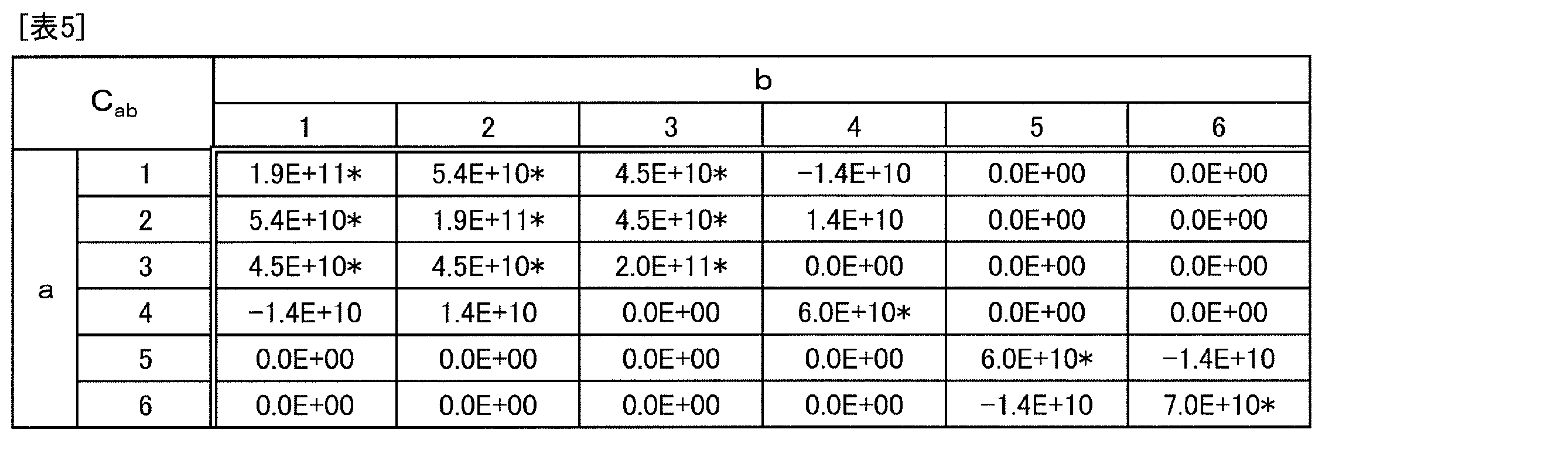

上記第2の実施形態及び第3の実施形態のインピーダンス特性を図6に示す。図6の実線が第2の実施形態の結果を、破線が第3の実施形態の結果を示す。図6から明らかなように、第3の実施形態に比べ、第2の実施形態によれば、5400MHz付近に現れている高次モードがより一層効果的に抑制されていることがわかる。 FIG. 6 shows impedance characteristics of the second embodiment and the third embodiment. The solid line in FIG. 6 shows the result of the second embodiment, and the broken line shows the result of the third embodiment. As is apparent from FIG. 6, it can be seen that, according to the second embodiment, higher-order modes appearing in the vicinity of 5400 MHz are more effectively suppressed than in the third embodiment.
なお、図7は、座標系(X,Y,Z)とオイラー角(φ,θ,ψ)との関係を示す模式図である。 FIG. 7 is a schematic diagram showing the relationship between the coordinate system (X, Y, Z) and Euler angles (φ, θ, ψ).
本明細書において、オイラー角(φ、θ、ψ)は、文献「弾性波素子技術ハンドブック」(日本学術振興会弾性波素子技術第150委員会、第1版第1刷、平成13年11月30日発行、549頁)記載の右手系オイラー角を用いた。シリコンの場合を例に説明すると、図21に示したようにシリコンの結晶軸をX軸、Y軸、Z軸と定義する。オイラー角(φ、θ、ψ)とは、右ネジの回転方向を正とし、図7に示すように、1)(X,Y,Z)をZ軸回りに「φ」回転し、(X1,Y1,Z1)とし、次に、2)(X1,Y1,Z1)をX1軸回りに「θ」回転し、(X2,Y2,Z2)とする。このZ2軸を法線とする面が材料層、または、圧電体の主面となる。さらに3)(X2,Y2,Z2)をZ2軸回りに「ψ」回転し、(X3,Y3,Z3)とする。このとき、前述の回転操作をオイラー角で(φ、θ、ψ)と表す。 In this specification, Euler angles (φ, θ, ψ) are based on the document “Acoustic Wave Element Technology Handbook” (Japan Society for the Promotion of Science Elastic Wave Element Technology 150th Committee, 1st edition, 1st edition, November 2001). The right-handed Euler angles described on the 30th, page 549) were used. The case of silicon will be described as an example. As shown in FIG. 21, the crystal axes of silicon are defined as an X axis, a Y axis, and a Z axis. Euler angles (φ, θ, ψ) are positive rotation directions of the right-hand screw. As shown in FIG. 7, 1) (X, Y, Z) is rotated “φ” around the Z axis, and (X 1 , Y 1 , Z 1 ), and 2) (X 1 , Y 1 , Z 1 ) is rotated by “θ” about the X 1 axis to be (X 2 , Y 2 , Z 2 ). Face material layer to the Z 2 axis and the normal line, or a major surface of the piezoelectric body. 3) (X 2 , Y 2 , Z 2 ) is rotated by “ψ” about the Z 2 axis to obtain (X 3 , Y 3 , Z 3 ). At this time, the above-described rotation operation is expressed as (φ, θ, ψ) in terms of Euler angles.
式(1)で示した弾性定数とは、材料層、または、圧電体の弾性定数の文献値に対して、前述した回転操作により弾性定数を座標変換したのちの弾性定数のことを言う。つまり、同一の材料であっても、使用するオイラー角により、弾性定数の各成分は各種値、符号を取り得る。 The elastic constant represented by the formula (1) refers to an elastic constant obtained by performing coordinate conversion of the elastic constant by the above-described rotation operation with respect to the literature value of the elastic constant of the material layer or the piezoelectric body. That is, even with the same material, each component of the elastic constant can take various values and signs depending on the Euler angle used.
また、材料層と圧電体のオイラー角がいずれも(0°,0°,0°)の場合における、両者の座標軸の関係を図25に示す。図25のX、Y、Z軸を材料層の結晶軸、図25のXa、Ya、Zaが圧電体の結晶軸である。オイラー角が(0°,0°,0°)の場合には図25に示したように、XとXa、YとYa、ZとZaが同一方向となるように定義する。圧電体を伝搬する弾性波がX伝搬の場合には、Xa方向とIDT電極が垂直となる。 Further, FIG. 25 shows the relationship between the coordinate axes of the material layer and the piezoelectric body when the Euler angles are (0 °, 0 °, 0 °). The X, Y, and Z axes in FIG. 25 are the crystal axes of the material layer, and Xa, Ya, and Za in FIG. 25 are the crystal axes of the piezoelectric body. When the Euler angles are (0 °, 0 °, 0 °), as shown in FIG. 25, X and Xa, Y and Ya, and Z and Za are defined in the same direction. When the elastic wave propagating through the piezoelectric body is X propagation, the Xa direction and the IDT electrode are perpendicular to each other.
弾性定数Cabと、応力Ta及び歪みSbとの間には、下記の式(3)に示す関係がある。 And the elastic constants C ab, between the stress T a and strain S b, relationship shown by the following equation (3).

なお、表4及び表5では、上記弾性定数の有効数字は2桁とされている。 In Tables 4 and 5, the effective number of the elastic constant is two digits.
また、絶対値が1×10⁹N/m2以下の弾性定数は値自体が小さく、高次モードに与える影響が小さいためゼロとみなす。逆に言うと、本発明による高次モード抑制の効果を得るためには、絶対値が1×109N/m2以上の弾性定数の符号を反転させる必要がある。 An elastic constant having an absolute value of 1 × 10 9 N / m 2 or less is regarded as zero because the value itself is small and the influence on the higher-order mode is small. In other words, in order to obtain the effect of suppressing higher-order modes according to the present invention, it is necessary to invert the sign of an elastic constant having an absolute value of 1 × 10 9 N / m 2 or more.
また、表4及び表5において*を付けた欄では、弾性定数はψの180°回転では値が変化しない。これに対して、0でない残りの弾性定数は、ψを180°回転した場合、絶対値は変わらないが、符号が変化する。この符号が変化する弾性定数としては、C41、C42、C65及びこれらと対称なC14、C24及びC56などが挙げられる。 In the columns marked with * in Tables 4 and 5, the value of the elastic constant does not change when ψ is rotated 180 °. On the other hand, the remaining elastic constants which are not 0 do not change in absolute value when ψ is rotated by 180 °, but the sign changes. Examples of the elastic constant whose sign changes include C 41 , C 42 , C 65, and C 14 , C 24, and C 56 that are symmetrical to these.
また、シリコン単結晶の結晶方位が(-45°,-54.7°,0°)と(-45°,-54.7°,180°)の場合のシリコン単結晶の弾性定数C41(=C14)、C42(=C24)及びC65(=C56)の符号は、下記の表7に示す通りである。 Further, the elastic constant C 41 of the silicon single crystal when the crystal orientation of the silicon single crystal is (−45 °, −54.7 °, 0 °) and (−45 °, −54.7 °, 180 °). = C 14 ), C 42 (= C 24 ) and C 65 (= C 56 ) are as shown in Table 7 below.

他方、LiTaO3のオイラー角は(0°,140°,0°)であり、この場合、LiTaO3の弾性定数は下記の表8に示す通りである。すなわち、第2の実施形態及び第3の実施形態における圧電体の弾性定数は表8に示す通りである。 On the other hand, the Euler angles of LiTaO 3 are (0 °, 140 °, 0 °). In this case, the elastic constant of LiTaO 3 is as shown in Table 8 below. That is, the elastic constants of the piezoelectric bodies in the second embodiment and the third embodiment are as shown in Table 8.

従って、表8におけるC41=C14、C42=C24及びC65=C56の符号は、以下の表9に示す通りとなる。 Therefore, the codes of C 41 = C 14 , C 42 = C 24 and C 65 = C 56 in Table 8 are as shown in Table 9 below.

すなわち、シリコン単結晶の結晶方位がオイラー角で(-45°,-54.7°,180°)とした場合、(-45°,-54.7°,0°)の場合と比べ、C41及びC65において符号は逆転されていることがわかる。 That is, when the crystal orientation of the silicon single crystal is Euler's angle (−45 °, −54.7 °, 180 °), compared to the case of (−45 °, −54.7 °, 0 °), C in 41 and C 65 codes it can be seen to be reversed.
ところで、上記弾性定数C41~C43、C51~C54及びC61~C65並びにこれらと対称な位置にある弾性定数のうち、圧電体3の弾性定数と材料層2の弾性定数とで1つの弾性定数のみ逆符号とした場合のインピーダンス特性を図8~図10にそれぞれ示す。構造は第2の実施形態に記載した構造で、LiTaO3のオイラー角は(0°,140°,0°)、シリコンのオイラー角が(-45°,-54.7°,0°)の場合の弾性定数を基準として、C41(=C14)、C42(=C24)、C65(=C56)の値を適宜変更して評価を行った。なお、基準とした構造では、LiTaO3の弾性波装置と、シリコンの弾性波装置とは全て同符号である。この基準とした構造の波形を図8~10の破線で示す。
By the way, among the elastic constants C 41 to C 43 , C 51 to C 54 and C 61 to C 65 and elastic constants at positions symmetrical thereto, the elastic constant of the
図8の実線は、圧電体3の弾性定数C41(=C14)の符号と、材料層2の弾性定数C41(=C14)の符号のみを、逆符号とした場合、破線は、弾性定数C41(=C14)を同符号とした場合の弾性波装置のインピーダンス特性を示す。図8に示すように、符号の反転により高次モードがわずかに抑制されていることがわかる。
The solid line in FIG. 8 indicates that when only the sign of the elastic constant C 41 (= C 14 ) of the
図9の実線は、圧電体3の弾性定数C42(=C24)の符号と、材料層2の弾性定数C41(=C14)の符号のみを逆符号とした場合の弾性波装置のインピーダンス特性を示す。破線は、弾性定数C42(=C24)を同符号とした場合の弾性波装置のインピーダンス特性を示す。
The solid line in FIG. 9 shows the acoustic wave device in the case where only the sign of the elastic constant C 42 (= C 24 ) of the
図10の実線は、圧電体3の弾性定数C56(=C65)の符号と、材料層2の弾性定数C41(=C14)の符号のみを、逆符号とした場合の弾性波装置のインピーダンス特性を示す。図10においても、破線は、弾性定数C56(=C65)が逆符号とされていない弾性波装置のインピーダンス特性を示す。
The solid line in FIG. 10 shows an elastic wave device in which only the sign of the elastic constant C 56 (= C 65 ) of the
図9から明らかなように、圧電体3の弾性定数C42の符号と、材料層2の弾性定数C41(=C14)の符号のみを逆符号とした場合、高次モードを効果的に抑圧し得ることがわかる。さらに、図10に示すように、弾性定数C56の符号を反転させた場合には、高次モードをより一層効果的に抑制でき、高次モードによる応答がほぼ現れていないことがわかる。
As apparent from FIG. 9, when only the sign of the elastic constant C 42 of the
従って、好ましくは、弾性定数C41、C42及びC56のうち、弾性定数C56=C65の符号を反転させることがもっとも好ましく、弾性定数C42=C24を逆符号とすることが次に好ましいことがわかる。 Therefore, it is most preferable to reverse the sign of the elastic constant C 56 = C 65 out of the elastic constants C 41 , C 42, and C 56 , and it is next preferable that the elastic constant C 42 = C 24 is reversed. It can be seen that it is preferable.
従って、本発明においては、圧電体3の弾性定数と材料層2の弾性定数とで逆符号とされている弾性定数は、弾性定数C41を含むことが好ましく、より好ましくは、弾性定数C42を含むことが好ましく、さらに好ましくは弾性定数C56またはC65を含むことが望ましい。
Accordingly, in the present invention, the elastic constants are the opposite sign in the elastic constants and elastic constants of the
なお、第1の実施形態及び第2の実施形態では、材料層2は、シリコン単結晶からなったが、サファイア、ダイヤモンド、SiC、GaN、AlN、GaAs、各種金属材料等の他の単結晶材料を用いても同様の効果が得られる。加えて、単結晶に限らず、弾性定数が式(1)で表される材料からなる材料層2であれば、同様の効果が得られる。シリコンの場合は熱伝導率が高く、放熱性が良好である。また、熱線膨張係数が小さく、温度特性の改善が可能となる。ダイシング等の加工性も良好で、材料層がシリコンであることが好ましい。
In the first embodiment and the second embodiment, the
もっとも、材料層は単結晶からなることが好ましく、圧電体以外の単結晶からなる材料層であることがより好ましい。圧電体の場合には、圧電効果を発現するため、新たな高次モードを生じるおそれがある。これに対して、圧電体以外の単結晶からなる材料層を用いることにより、このようなさらなる高次モードの影響を受け難い。 However, the material layer is preferably made of a single crystal, and more preferably a material layer made of a single crystal other than the piezoelectric body. In the case of a piezoelectric body, since a piezoelectric effect is exhibited, there is a possibility that a new higher order mode is generated. On the other hand, by using a material layer made of a single crystal other than the piezoelectric body, it is difficult to be influenced by such higher order modes.
また、第1及び第2の実施形態では、Li2B4O7またはLiTaO3を用いたが、圧電体を構成する圧電単結晶についてもこれらに限定されるものではない。 In the first and second embodiments, Li 2 B 4 O 7 or LiTaO 3 is used, but the piezoelectric single crystal constituting the piezoelectric body is not limited to these.
(第3の実施形態)
第3の実施形態では、シリコン単結晶のオイラー角が(-45°,-54.7°,0°)の場合の弾性定数に対し、弾性定数C56=C65の値のみを変化した架空の弾性定数を持つ材料層を用いた。その他の内容は第2の実施形態と同様とした。
(Third embodiment)
In the third embodiment, an imaginary in which only the value of the elastic constant C 56 = C 65 is changed with respect to the elastic constant when the Euler angle of the silicon single crystal is (−45 °, −54.7 °, 0 °). A material layer having an elastic constant of The other contents are the same as in the second embodiment.
この場合において、C56=C65の値を種々変化させた。 In this case, the value of C 56 = C 65 was changed variously.
図11は、弾性定数C56の大きさと、高次モードの位相最大値との関係を示す図である。LiTaO3のオイラー角が(0°,140°,0°)の場合、弾性定数C56は、-3.7GPaであり、負の値である。 FIG. 11 is a diagram showing the relationship between the magnitude of the elastic constant C 56 and the phase maximum value of the higher-order mode. Euler angles of the LiTaO 3 is (0 °, 140 °, 0 °) For the elastic constants C 56 is -3.7GPa, is a negative value.
従って、シリコン単結晶の弾性定数C56が正であれば、高次モードを抑制することができる。図11に示すように、シリコン単結晶の弾性定数C56の値が0よりも正の値で大きい領域において、高次モードの位相最大値を-70°レベルまで抑制し得ることがわかる。従って、シリコン単結晶の弾性定数C56が0よりも大きい値であれば、弾性定数C56の大きさに依存せずに、高次モードを効果的に抑制することができる。より好ましくは、1GPa以上とすることで、高次モードをより効果的に抑制することが可能となる。すなわち、高次モードの抑制では、弾性定数の絶対値には依存しないことがわかる。
Accordingly, the elastic constant C 56 of the silicon single crystal, if positive, it is possible to suppress higher order modes. As shown in FIG. 11, in the region greater positive value than the
(第4の実施形態)
第4の実施形態では、第2の実施形態において、LiTaO3からなる圧電体3の膜厚を0.05λ~15λの範囲で変化させた。
(Fourth embodiment)
In the fourth embodiment, the film thickness of the
LiTaO3の結晶方位はオイラー角で(0°,140°,0°)とし、シリコン単結晶の結晶方位はオイラー角で(-45°,-54.7°,0°)または(-45°,-54.7°,180°)とした。 The crystal orientation of LiTaO 3 is Euler angles (0 °, 140 °, 0 °), and the crystal orientation of a silicon single crystal is Euler angles (−45 °, −54.7 °, 0 °) or (−45 ° , −54.7 °, 180 °).
図12の横軸は圧電体の膜厚すなわちLiTaO3の膜厚であり、縦軸は高次モード位相差(°)である。ここで、高次モード位相差とは、シリコン単結晶のオイラー角が(-45°,-54.7°,0°)の場合の高次モード位相差最大値と、(-45°,-54.7°,180°)である場合の高次モード位相差最大値との差を示す。この高次モード位相差の差が大きいほど、高次モード強度の改善度が大きい。 The horizontal axis of FIG. 12 is the film thickness of the piezoelectric body, that is, the film thickness of LiTaO 3 , and the vertical axis is the higher-order mode phase difference (°). Here, the high-order mode phase difference is the maximum value of the high-order mode phase difference when the Euler angle of the silicon single crystal is (−45 °, −54.7 °, 0 °), and (−45 °, − The difference from the maximum value of the higher-order mode phase difference in the case of 54.7 ° and 180 °) is shown. The higher the higher-order mode phase difference, the greater the improvement in higher-order mode strength.
図12から明らかなように、圧電体の膜厚が薄い方が高次モードの改善度が高い。これは、圧電体が薄いと、シリコン単結晶からなる材料層内へより多くのエネルギーが分布し、高次モード抑制効果が高まるためと考えられる。 As is clear from FIG. 12, the degree of improvement in the higher-order mode is higher as the piezoelectric film is thinner. This is presumably because if the piezoelectric material is thin, more energy is distributed in the material layer made of silicon single crystal, and the higher-order mode suppression effect is enhanced.
また、図12によれば、高次モード抑制効果は、圧電体の膜厚が、10λ以下の領域で効果的であることがわかる。従って、好ましくは、圧電体の膜厚は、10λ以下であることが望ましい。 Further, according to FIG. 12, it can be seen that the high-order mode suppression effect is effective in the region where the film thickness of the piezoelectric body is 10λ or less. Therefore, the thickness of the piezoelectric body is preferably 10λ or less.
(第5の実施形態)
図13は、本発明の第5の実施形態に係る弾性波装置の正面断面図である。
(Fifth embodiment)
FIG. 13 is a front sectional view of an acoustic wave device according to a fifth embodiment of the present invention.
弾性波装置21では、材料層2と、圧電体3との間に、低音速膜22が積層されている。低音速膜22は、伝搬するバルク波の音速が、圧電体3を伝搬する弾性波の音速よりも低い低音速材料からなる。この低音速膜22は、本実施形態では、酸化ケイ素からなる。なお、酸化ケイ素はSiO2であってもよい。低音速膜を構成する材料としては圧電膜を伝搬する弾性波よりも低音速のバルク波音速を有する適宜の材料を用いることができる。このような低音速材料としては、酸化ケイ素、ガラス、酸窒化ケイ素、酸化タンタル、または、酸化ケイ素にフッ素や炭素やホウ素を加えた化合物など、当該材料を主成分とした媒質を用いることができる。
In the
第5の実施形態の弾性波装置においても、材料層2と圧電体3との間で、前述した式(1)で表される弾性定数C11~C66のうち、0でない少なくとも1つの弾性定数が、逆符号とされておればよい。それによって、第1~第4の実施形態と同様に、高次モードを抑制することができる。これを、より具体的な実験例に基づき説明する。
Also in the elastic wave device of the fifth embodiment, at least one elasticity which is not 0 among the elastic constants C 11 to C 66 represented by the above-described formula (1) between the
第5の実施形態の弾性波装置21において、LiTaO3からなる圧電体3の厚みを0.3λ、オイラー角を(0°,140°,0°)とした。酸化ケイ素膜として、SiO2膜を用いた。そしてSiO2膜からなる低音速膜22の厚みは0.35λとした。材料層2として用いたシリコン単結晶のオイラー角を第2の実施形態の場合と同様に、(-45°,-54.7°,0°)または(-45°,-54.7°,180°)とした。
In the
IDT電極4の電極指ピッチで定まる波長λは1.0μm、IDT電極4は、Alからなり、その膜厚は0.08λとした。
The wavelength λ determined by the electrode finger pitch of the
図14の実線は、第5の実施形態の結果を示し、シリコン単結晶のオイラー角が(-45°,-54.7°,180°)の場合のインピーダンス特性である。破線は、第2の比較例の特性を示し、シリコン単結晶のオイラー角は(-45°,-54.7°,0°)である。破線で示す特性に比べ、実線で示す特性によれば、5.1GHz付近に現れている高次モードを効果的に抑制し得ることがわかる。 The solid line in FIG. 14 shows the result of the fifth embodiment, and shows the impedance characteristics when the Euler angles of the silicon single crystal are (−45 °, −54.7 °, 180 °). The broken line indicates the characteristics of the second comparative example, and the Euler angles of the silicon single crystal are (−45 °, −54.7 °, 0 °). It can be seen that the higher-order mode appearing in the vicinity of 5.1 GHz can be effectively suppressed according to the characteristic indicated by the solid line compared to the characteristic indicated by the broken line.
このように、圧電体3と材料層2との間に低音速膜22を設けてもよい。この場合、低音速膜22を設けることにより、圧電体3への弾性波のエネルギー集中度を高めることができる。それによって損失を小さくすることができる。また、SiO2からなる低音速膜22の場合には、周波数温度特性を改善することができる。さらに、WO2012/086639に開示されているように、SiO2膜の膜厚を2λ以下とすることにより、電気機械結合係数を調整することができる。
Thus, the low
(第6の実施形態)
図15は、第6の実施形態に係る弾性波装置の正面断面図である。弾性波装置31は、低音速膜22と、材料層2との間に高音速膜32が積層されている。その他の構成は、弾性波装置31は、弾性波装置21と同様である。高音速膜32は、伝搬するバルク波の音速が、圧電体3を伝搬する弾性波の音速よりも高速である高音速材料からなる。このような高音速材料は、上記音速関係を満たす限り特に限定されない。低音速膜22は、前述した適宜の低音速材料で構成し得るが、本実施形態では、低音速膜22は酸化ケイ素である。また、高音速膜32は、窒化ケイ素である。
(Sixth embodiment)
FIG. 15 is a front sectional view of an acoustic wave device according to a sixth embodiment. In the
高音速膜32用の高音速材料としては、窒化アルミニウム、酸化アルミニウム、炭化ケイ素、窒化ケイ素、酸窒化ケイ素、シリコン、サファイア、タンタル酸リチウム、ニオブ酸リチウム、水晶、アルミナ、ジルコニア、コ-ジライト、ムライト、ステアタイト、フォルステライト、マグネシア、DLC膜またはダイヤモンド、これらの材料を主成分とする媒質、これらの材料の混合物を主成分とする媒質等が用いられ得る。
High sound velocity materials for the high
このように、高音速膜32をさらに積層した弾性波装置31でも、材料層2の弾性定数C41~C43、C51~C54、及びC61~C65並びにこれらと対称な位置にある弾性定数の少なくとも1つの弾性定数と、圧電体3の弾性定数C41~C43、C51~C54、及びC61~C65並びにこれらと対称な位置にある弾性定数の少なくとも1つの弾性定数とが逆符号とされておればよい。それによって、高次モードを抑制することができる。これを、図16及び図17に示す。
As described above, the
窒化ケイ素からなる高音速膜の膜厚を0.45λとした。LiTaO3のオイラー角は、(0°,140°,0°)とし、シリコン単結晶のオイラー角は、第6の実施形態において(-45°,-54.7°,180°)とした。その他の構成は、第5の実施形態と同様にして、第6の実施形態に係る弾性波装置を用意した。比較のために、第5の実施形態の弾性波装置を用意した。 The film thickness of the high acoustic velocity film made of silicon nitride was 0.45λ. The Euler angles of LiTaO 3 were (0 °, 140 °, 0 °), and the Euler angles of the silicon single crystal were (−45 °, −54.7 °, 180 °) in the sixth embodiment. Other configurations were the same as in the fifth embodiment, and an elastic wave device according to the sixth embodiment was prepared. For comparison, an acoustic wave device according to the fifth embodiment was prepared.
図16及び図17は、第6の実施形態及び第5の実施形態の弾性波装置の位相特性を示す図である。図16及び図17において実線が第6の実施形態の結果を、破線が第5の実施形態の結果を示す。破線に比べ実線の特性によれば、4600~4700MHz付近の高次モードを抑制し得ることがわかる。また、4700~5000MHz付近における位相特性が-90°に近いため、損失の低減も果たすことが可能となっている。さらに、5000~6000MHz付近に、弱い応答の高次モードが生じている。しかしながら、窒化ケイ素膜を有しない場合に比べ、高次モードの応答(位相最大値)のピーク自体は小さくなっている。 16 and 17 are diagrams showing the phase characteristics of the acoustic wave devices of the sixth embodiment and the fifth embodiment. 16 and 17, the solid line indicates the result of the sixth embodiment, and the broken line indicates the result of the fifth embodiment. According to the characteristics of the solid line as compared with the broken line, it can be seen that higher-order modes around 4600 to 4700 MHz can be suppressed. Further, since the phase characteristic in the vicinity of 4700 to 5000 MHz is close to −90 °, it is possible to reduce the loss. Further, a high-order mode having a weak response is generated in the vicinity of 5000 to 6000 MHz. However, the peak of the higher-order mode response (phase maximum value) itself is smaller than when the silicon nitride film is not provided.
すなわち、高音速膜32を設けることにより、高次モードをより一層効果的に抑制し得ることがわかる。
That is, it can be seen that the high-order mode can be more effectively suppressed by providing the high
(第7の実施形態)
第7の実施形態として、第6の実施形態の弾性波装置31において、高音速膜32としての窒化ケイ素膜の膜厚を変化させた。図18は窒化ケイ素膜の膜厚と、高次モードの位相最大値との関係を示す図である。
(Seventh embodiment)
As the seventh embodiment, in the
図18から明らかなように、窒化ケイ素膜の膜厚が、0.25λ以上になると、高次モードの強度がほぼ-90°付近まで低下することがわかる。従って、好ましくは、窒化ケイ素膜の膜厚は0.25λ以上である。なお、図19は、窒化ケイ素膜の膜厚を変化させた場合の4000MHz~6000MHzの帯域に発生する高次モードの位相最大値の変化を示す図である。 As can be seen from FIG. 18, when the thickness of the silicon nitride film is 0.25λ or more, the intensity of the higher-order mode decreases to approximately −90 °. Therefore, preferably, the thickness of the silicon nitride film is 0.25λ or more. FIG. 19 is a diagram showing a change in the phase maximum value of the higher-order mode generated in the 4000 MHz to 6000 MHz band when the thickness of the silicon nitride film is changed.
図19から明らかなように、窒化ケイ素膜の膜厚を0.55λ以下とすれば、4000MHz~6000MHzに現れる高次モードの位相を-60°よりも小さくし得ることがわかる。 As is apparent from FIG. 19, it can be seen that if the thickness of the silicon nitride film is 0.55λ or less, the phase of the higher-order mode appearing at 4000 MHz to 6000 MHz can be made smaller than −60 °.
従って、メインモードからもっとも近い高次モードを抑制しつつ、高次モードの全体のレベルを抑制するには、窒化ケイ素膜の膜厚は0.25λ以上、0.55λ以下の範囲とするのが望ましいことがわかる。 Therefore, in order to suppress the higher-order mode closest to the main mode while suppressing the overall level of the higher-order mode, the film thickness of the silicon nitride film should be in the range of 0.25λ to 0.55λ. It turns out to be desirable.
図20は、第1の実施形態の変形例に係る弾性波装置の正面断面図である。図20に示す弾性波装置51では、材料層2の圧電体3と接触している側の面とは反対側の面に支持基板52が積層されている。このように、材料層2を支持している支持基板52がさらに備えられていてもよい。支持基板52を構成する材料としては、特に限定されず、アルミナ、シリコンなどの適宜の絶縁性セラミックスや、金属などを用いることができる。
FIG. 20 is a front cross-sectional view of an elastic wave device according to a modification of the first embodiment. In the
(第8の実施形態)
第8の実施形態に係る弾性波装置の積層構造は、第1の実施形態の弾性波装置と同様である。もっとも、積層構造は以下のとおりである。シリコンからなる厚み0.1λの材料層上に、厚み0.3λのLiTaO3からなる圧電体が積層されている。この圧電体上に、厚み0.08λのAlからなるIDT電極が設けられている。LiTaO3のオイラー角を(0°,140°,0°)とし、シリコンのオイラー角は第8の実施形態では、(-45°,-54.7°,180°)とした。また、第3の比較例として、シリコンのオイラー角が、(-45°,-54.7°,0°)であることを除いては、第8の実施形態と同様にして弾性波装置を作製した。シリコンからなる材料層の下面を無反射吸収端としてシミュレーションし、高次モードの応答を調べた。
(Eighth embodiment)
The laminated structure of the elastic wave device according to the eighth embodiment is the same as that of the elastic wave device of the first embodiment. However, the laminated structure is as follows. A piezoelectric body made of LiTaO 3 having a thickness of 0.3λ is laminated on a material layer made of silicon and having a thickness of 0.1λ. An IDT electrode made of Al having a thickness of 0.08λ is provided on the piezoelectric body. The Euler angles of LiTaO 3 were (0 °, 140 °, 0 °), and the Euler angles of silicon were (−45 °, −54.7 °, 180 °) in the eighth embodiment. Further, as a third comparative example, an elastic wave device is manufactured in the same manner as in the eighth embodiment except that the Euler angles of silicon are (−45 °, −54.7 °, 0 °). Produced. The lower surface of the material layer made of silicon was simulated as a reflection-free absorption edge, and the response of higher-order modes was investigated.
図22の実線は、第8の実施形態の結果を、破線は第3の比較例の結果を示す。第8の実施形態においても、弾性定数の符号が、圧電体と材料層とで逆符号とされている。そのため、図22から明らかなように高次モードを効果的に抑制し得ることがわかる。このように、材料層は厚みのある支持基板ではなく、薄い材料層であってもよい。また、第8の実施形態のように、板波のモードを励振する構造においても、高次モードを抑制することができる。 22 indicates the result of the eighth embodiment, and the broken line indicates the result of the third comparative example. Also in the eighth embodiment, the sign of the elastic constant is reversed between the piezoelectric body and the material layer. Therefore, it can be seen from FIG. 22 that the higher-order mode can be effectively suppressed. Thus, the material layer may be a thin material layer instead of a thick support substrate. Further, even in a structure that excites a plate wave mode as in the eighth embodiment, higher-order modes can be suppressed.
(第9の実施形態)
図23は、第9の実施形態に係る弾性波装置の正面断面図である。弾性波装置61は、126.5°Yカットのニオブ酸リチウムからなる圧電体62を有する。圧電体62上に、IDT電極63が設けられている。IDT電極63は、Pt膜上に、Al膜が積層されている積層金属膜とした。Al膜の厚みは0.06λ、Pt膜の厚みは0.02λとした。
(Ninth embodiment)
FIG. 23 is a front sectional view of the acoustic wave device according to the ninth embodiment. The
また、IDT電極63を覆うように、厚み0.3λの酸化ケイ素膜(SiO2膜)64が積層されており、酸化ケイ素膜64上に、シリコンからなる材料層65が積層されている。このように、圧電体62のIDT電極63が設けられている主面に間接に材料層65が積層されている。第9の実施形態では、シリコンのオイラー角は(-45°,-54.7°,180°)とした。第4の比較例として、シリコンのオイラー角が(-45°,-54.7°,0°)としたことを除いては、第9の実施形態と同様にして弾性波装置を作製した。
A silicon oxide film (SiO 2 film) 64 having a thickness of 0.3λ is laminated so as to cover the
図24は、第9の実施形態及び第4の比較例において、ニオブ酸リチウムを伝搬するレイリー波を利用した場合の高次モードの応答を示す図である。図24の破線で示すように、第4の比較例では、高次モードの応答が4040MHz付近において強く現れているのに対し、実線で示す第9の実施形態では、高次モードの応答がほとんど流れていないことがわかる。図24から、この場合においても、圧電体と材料層とで弾性定数を逆符号とすることにより、高次モードを抑制し得ることがわかる。 FIG. 24 is a diagram showing a higher-order mode response when Rayleigh waves propagating through lithium niobate are used in the ninth embodiment and the fourth comparative example. As shown by the broken line in FIG. 24, in the fourth comparative example, the response of the higher-order mode appears strongly in the vicinity of 4040 MHz, whereas in the ninth embodiment shown by the solid line, the response of the higher-order mode is almost the same. You can see that it is not flowing. FIG. 24 shows that even in this case, higher-order modes can be suppressed by setting the elastic constants of the piezoelectric body and the material layer to opposite signs.
(圧電体の厚み及び酸化ケイ素膜の厚み)
LiTaO3膜からなる圧電体の膜厚は、3.5λ以下が好ましい。その場合には、3.5λを超えた場合に比べて、Q値が高くなる。より好ましくは、Q値をより高めるには、LiTaO3膜の膜厚は、2.5λ以下であることが望ましい。
(Piezoelectric thickness and silicon oxide film thickness)
The film thickness of the piezoelectric body made of the LiTaO 3 film is preferably 3.5λ or less. In that case, the Q value becomes higher than that in the case of exceeding 3.5λ. More preferably, in order to further increase the Q value, the thickness of the LiTaO 3 film is desirably 2.5λ or less.
また、圧電体の膜厚が、2.5λ以下の場合、周波数温度係数TCFの絶対値が2.5λを超えた場合に比べて小さくすることができる。より好ましくは、膜厚を2λ以下とすることが望ましく、その場合には、周波数温度係数TCFの絶対値を、10ppm/℃以下とし得る。周波数温度係数TCFの絶対値を小さくするには、圧電体の膜厚を1.5λ以下とすることがさらに好ましい。 Further, when the film thickness of the piezoelectric body is 2.5λ or less, the absolute value of the frequency temperature coefficient TCF can be made smaller than that when the absolute value exceeds 2.5λ. More preferably, the film thickness is desirably 2λ or less, and in that case, the absolute value of the frequency temperature coefficient TCF can be 10 ppm / ° C. or less. In order to reduce the absolute value of the frequency temperature coefficient TCF, the film thickness of the piezoelectric body is more preferably set to 1.5λ or less.
電気機械結合係数及び比帯域の調整範囲を広げるためには、LiTaO3膜の膜厚は、0.05λ以上、0.5λ以下の範囲が望ましい。 In order to widen the adjustment range of the electromechanical coupling coefficient and the specific band, the thickness of the LiTaO 3 film is desirably in the range of 0.05λ to 0.5λ.
また、酸化ケイ素膜の圧電体とは反対側の面に高音速膜として、さまざまな高音速材料からなる膜を積層することができる。この場合の高音速膜としては、窒化ケイ素膜、酸化アルミニウム膜またはDLC膜などを用いることができる。 Also, a film made of various high sound speed materials can be laminated as a high sound speed film on the surface of the silicon oxide film opposite to the piezoelectric body. In this case, as the high sound velocity film, a silicon nitride film, an aluminum oxide film, a DLC film, or the like can be used.
なお、この場合、高音速膜の材質及び酸化ケイ素膜の膜厚を変更したとしても、電気機械結合係数及び音速がほとんど変化しないことが確かめられている。特に、酸化ケイ素膜の膜厚が、0.1λ以上、0.5λ以下では、高音速膜の材質の如何に関わらず、電気機械結合係数はほとんど変わらない。また、酸化ケイ素膜の膜厚が、0.3λ以上、2λ以下であれば、高音速膜の材質の如何に関わらず、音速が変わらない。従って、好ましくは、酸化ケイ素からなる低音速膜の膜厚は、2λ以下、より望ましくは0.5λ以下であることが好ましい。 In this case, it has been confirmed that the electromechanical coupling coefficient and the sound speed hardly change even if the material of the high sound speed film and the film thickness of the silicon oxide film are changed. In particular, when the film thickness of the silicon oxide film is 0.1λ or more and 0.5λ or less, the electromechanical coupling coefficient hardly changes regardless of the material of the high acoustic velocity film. Moreover, if the film thickness of the silicon oxide film is 0.3λ or more and 2λ or less, the sound speed does not change regardless of the material of the high sound speed film. Therefore, preferably, the film thickness of the low acoustic velocity film made of silicon oxide is 2λ or less, more desirably 0.5λ or less.
(弾性波装置の構造)
本発明の弾性波装置は、弾性波共振子であってもよく、帯域通過型の弾性波フィルタであってもよく、弾性波装置の電極構造は特に限定されない。
(Structure of elastic wave device)
The elastic wave device of the present invention may be an elastic wave resonator or a band-pass elastic wave filter, and the electrode structure of the elastic wave device is not particularly limited.
図26は、高周波フロントエンド回路を有する通信装置の概略構成図である。通信装置240は、アンテナ202と、高周波フロントエンド回路230と、RF信号処理回路203とを有する。高周波フロントエンド回路230は、アンテナ202に接続される回路部分である。高周波フロントエンド回路230は、マルチプレクサ210と、増幅器221~224とを有する。マルチプレクサ210は、第1~第4のフィルタ211~214を有する。この第1~第4のフィルタ211~214に、上述した本発明の弾性波装置を用いることができる。マルチプレクサ210は、アンテナ202に接続されるアンテナ共通端子225を有する。アンテナ共通端子225、に受信フィルタとしての第1~第3のフィルタ211~213一端と、送信フィルタとしてのフィルタの214の一端とが共通接続されている。第1~第3のフィルタ211~213の出力端が、増幅器221~223にそれぞれ接続されている。また、第4のフィルタ214の入力端に、増幅器224が接続されている。
FIG. 26 is a schematic configuration diagram of a communication apparatus having a high-frequency front end circuit. The
増幅器221~223の出力端がRF信号処理回路203に接続されている。増幅器224の入力端がRF信号処理回路203に接続されている。
The output terminals of the
なお、マルチプレクサは、複数の送信フィルタのみを有するものであってもよく、複数の受信フィルタを有するものであってもよい。 Note that the multiplexer may have only a plurality of transmission filters, or may have a plurality of reception filters.
本発明の弾性波装置は、弾性波共振子、フィルタ、デュプレクサ、マルチバンドシステムに適用できるマルチプレクサ、フロントエンド回路及び通信装置として、携帯電話などの通信機器に広く利用できる。 The elastic wave device of the present invention can be widely used in communication devices such as mobile phones as an elastic wave resonator, a filter, a duplexer, a multiplexer applicable to a multiband system, a front-end circuit, and a communication device.
1…弾性波装置
2…材料層
3…圧電体
3a,3b…第1,第2の主面
4…IDT電極
5,6…反射器
21,31,51,61…弾性波装置
22…低音速膜
32…高音速膜
52…支持基板
62…圧電体
63…IDT電極
64…酸化ケイ素膜
65…材料層
202…アンテナ素子
203…RF信号処理回路
210…マルチプレクサ
211~214…第1~第4のフィルタ
221~224…増幅器
225…アンテナ共通端子
230…高周波フロントエンド回路
240…通信装置
DESCRIPTION OF
Claims (35)
対向し合う第1及び第2の主面を有し、前記第2の主面側から前記材料層に直接的にまたは間接的に積層されており、オイラー角(φ2,θ2,ψ2)を有し、前記オイラー角(φ2,θ2,ψ2)における弾性定数が下記の式(1)で表される圧電体と、
前記圧電体の前記第1の主面及び前記第2の主面のうちの少なくとも一方に設けられているIDT電極と、
を備え、
前記材料層の弾性定数C11~C66のうち0でない少なくとも1つの弾性定数と、前記圧電体の弾性定数C11~C66のうち0でない少なくとも1つの弾性定数とが逆符号となっている、弾性波装置。

The first and second main surfaces are opposed to each other, and are stacked directly or indirectly on the material layer from the second main surface side. The Euler angles (φ 2 , θ 2 , ψ 2 And a piezoelectric body whose elastic constant at the Euler angles (φ 2 , θ 2 , ψ 2 ) is represented by the following formula (1):
An IDT electrode provided on at least one of the first main surface and the second main surface of the piezoelectric body;
With
At least one elastic constant non-zero among the elastic constants C 11 ~ C 66 of the material layer, and at least one elastic constant non-zero among the elastic constants C 11 ~ C 66 of the piezoelectric body are opposite sign , Elastic wave device.
式中、α及びβは以下の通りである。
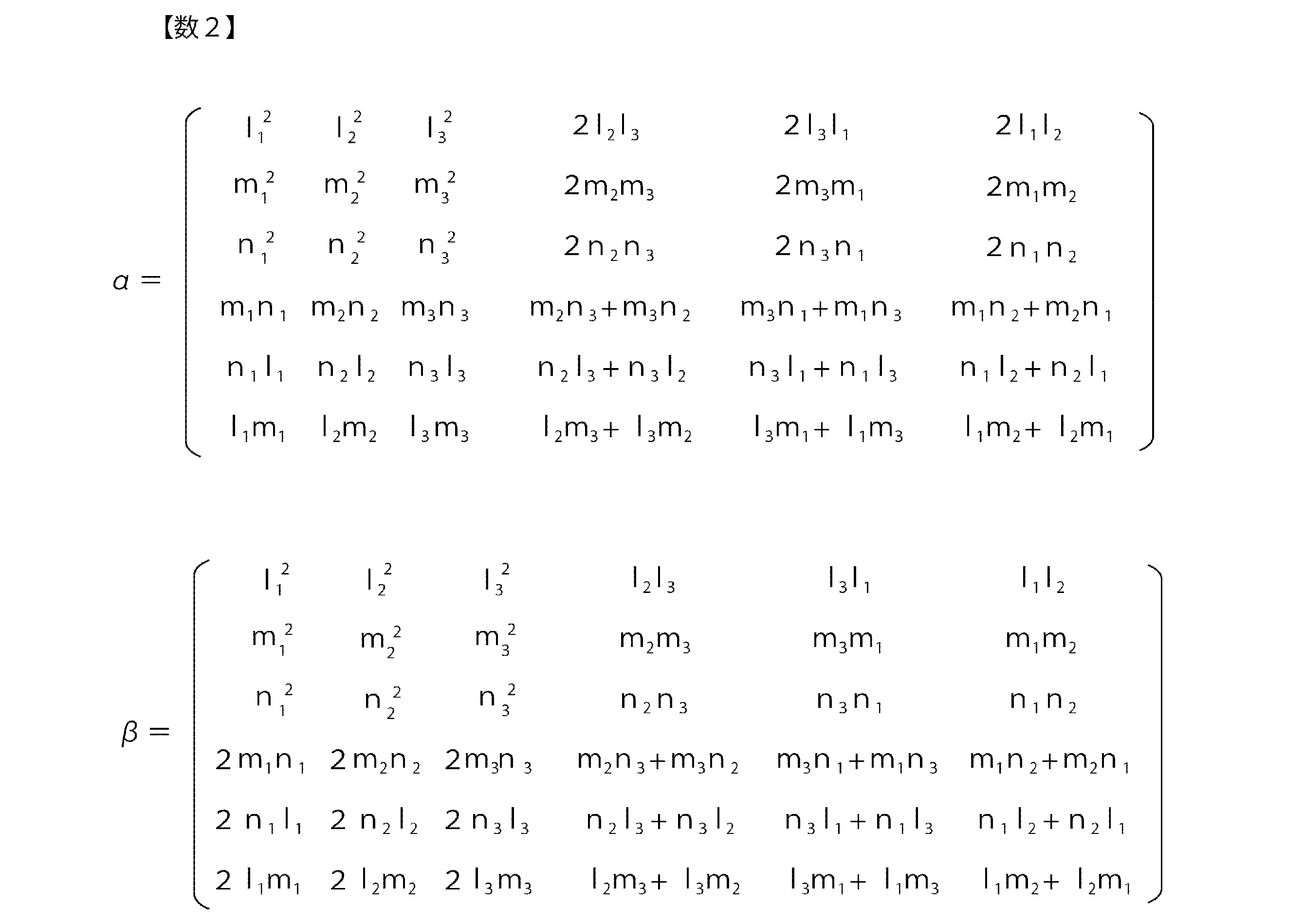
l1=cosψcosφ-cosθsinφsinψ
l2=-sinψcosφ-cosθsinφcosψ
l3=sinθsinφ
m1=cosψsinφ+cosθcosφsinψ
m2=-sinψsinφ+cosθcosφcosψ
m3=-sinθcosφ
n1=sinψsinθ
n2=cosψsinθ
n3=cosθ When the elastic constant c ab 0 before the rotation operation of the material layer, wherein the Euler angles (φ 1, θ 1, ψ 1) The elastic constant c ab in the formula (c ab) = [α] -1 [c ab 0] calculated by [beta], the elastic constant c ab in said Euler angles of the piezoelectric body (φ 2, θ 2, ψ 2) is the elastic constant of the piezoelectric body before rotating operation c ab when the 1, wherein (c ab) = [α] -1 obtained by [c ab 1] [β] , the acoustic wave device according to claim 1.
In the formula, α and β are as follows.
l 1 = cosψcosφ-cosθsinφsinψ
l 2 = −sinψcosφ-cosθsinφcosψ
l 3 = sinθsinφ
m 1 = cosψsinφ + cosθcosφsinψ
m 2 = −sinψsinφ + cosθcosφcosψ
m 3 = −sin θ cos φ
n 1 = sinψsinθ
n 2 = cosψsinθ
n 3 = cos θ
パワーアンプと、
を備える、高周波フロントエンド回路。 The elastic wave device according to any one of claims 1 to 33;
A power amplifier,
A high-frequency front-end circuit comprising:
RF信号処理回路と、
を備える、通信装置。 A high-frequency front-end circuit comprising the acoustic wave device according to any one of claims 1 to 33 and a power amplifier;
An RF signal processing circuit;
A communication device comprising:
Priority Applications (4)
| Application Number | Priority Date | Filing Date | Title |
|---|---|---|---|
| CN201880015091.2A CN110352557B (en) | 2017-03-09 | 2018-02-20 | elastic wave device |
| KR1020197025083A KR102311140B1 (en) | 2017-03-09 | 2018-02-20 | Acoustic wave devices, high-frequency front-end circuits and communication devices |
| JP2019504440A JP6725058B2 (en) | 2017-03-09 | 2018-02-20 | Elastic wave device, high-frequency front-end circuit, and communication device |
| US16/562,503 US11611324B2 (en) | 2017-03-09 | 2019-09-06 | Acoustic wave device, high frequency front end circuit, and communication apparatus |
Applications Claiming Priority (2)
| Application Number | Priority Date | Filing Date | Title |
|---|---|---|---|
| JP2017044690 | 2017-03-09 | ||
| JP2017-044690 | 2017-03-09 |
Related Child Applications (1)
| Application Number | Title | Priority Date | Filing Date |
|---|---|---|---|
| US16/562,503 Continuation US11611324B2 (en) | 2017-03-09 | 2019-09-06 | Acoustic wave device, high frequency front end circuit, and communication apparatus |
Publications (1)
| Publication Number | Publication Date |
|---|---|
| WO2018163805A1 true WO2018163805A1 (en) | 2018-09-13 |
Family
ID=63447613
Family Applications (1)
| Application Number | Title | Priority Date | Filing Date |
|---|---|---|---|
| PCT/JP2018/005991 Ceased WO2018163805A1 (en) | 2017-03-09 | 2018-02-20 | Elastic wave device, high-frequency front end circuit, and communications device |
Country Status (5)
| Country | Link |
|---|---|
| US (1) | US11611324B2 (en) |
| JP (2) | JP6725058B2 (en) |
| KR (1) | KR102311140B1 (en) |
| CN (1) | CN110352557B (en) |
| WO (1) | WO2018163805A1 (en) |
Cited By (7)
| Publication number | Priority date | Publication date | Assignee | Title |
|---|---|---|---|---|
| JP2020150415A (en) * | 2019-03-13 | 2020-09-17 | 太陽誘電株式会社 | Method for manufacturing elastic wave device, wafer, filter, and multiplexer |
| WO2020187825A1 (en) * | 2019-03-19 | 2020-09-24 | RF360 Europe GmbH | Saw resonator with reduced spurious modes, electro acoustic filter and multiplexer |
| WO2020209190A1 (en) * | 2019-04-08 | 2020-10-15 | 株式会社村田製作所 | Elastic wave device and multiplexer |
| JPWO2019082901A1 (en) * | 2017-10-24 | 2020-11-12 | 京セラ株式会社 | Composite substrate and elastic wave element using it |
| WO2021002382A1 (en) * | 2019-07-01 | 2021-01-07 | 株式会社村田製作所 | Elastic wave device |
| WO2021166875A1 (en) * | 2020-02-17 | 2021-08-26 | 株式会社村田製作所 | Acoustic wave device |
| WO2025243952A1 (en) * | 2024-05-20 | 2025-11-27 | 株式会社村田製作所 | Elastic wave device |
Families Citing this family (5)
| Publication number | Priority date | Publication date | Assignee | Title |
|---|---|---|---|---|
| JP6658957B2 (en) * | 2017-03-09 | 2020-03-04 | 株式会社村田製作所 | Elastic wave device, high-frequency front-end circuit, and communication device |
| JP6806907B2 (en) | 2017-07-27 | 2021-01-06 | 京セラ株式会社 | Elastic wave device, duplexer and communication device |
| CN110994097B (en) * | 2019-12-24 | 2021-12-07 | 无锡市好达电子股份有限公司 | High-frequency large-bandwidth thin-film bulk wave filter structure and preparation method thereof |
| CN115428337A (en) * | 2020-04-17 | 2022-12-02 | 株式会社村田制作所 | elastic wave device |
| US12341489B2 (en) | 2021-09-13 | 2025-06-24 | Rf360 Singapore Pte. Ltd. | Surface-acoustic-wave (SAW) filter with a compensation layer having multiple densities |
Citations (5)
| Publication number | Priority date | Publication date | Assignee | Title |
|---|---|---|---|---|
| JP2010011440A (en) * | 2008-05-30 | 2010-01-14 | Hitachi Ltd | Acoustic wave device and high-frequency filter using the same |
| WO2012073871A1 (en) * | 2010-11-30 | 2012-06-07 | 株式会社村田製作所 | Elastic wave device and method for manufacturing same |
| WO2013047433A1 (en) * | 2011-09-30 | 2013-04-04 | 株式会社村田製作所 | Elastic wave device |
| JP2015115870A (en) * | 2013-12-13 | 2015-06-22 | 株式会社村田製作所 | Acoustic wave device |
| WO2017043394A1 (en) * | 2015-09-10 | 2017-03-16 | 株式会社村田製作所 | Elastic wave device, high-frequency front-end circuit and communication device |
Family Cites Families (9)
| Publication number | Priority date | Publication date | Assignee | Title |
|---|---|---|---|---|
| JP3880150B2 (en) | 1997-06-02 | 2007-02-14 | 松下電器産業株式会社 | Surface acoustic wave device |
| JP2003229741A (en) * | 2001-11-30 | 2003-08-15 | Mitsubishi Materials Corp | Substrate for surface acoustic wave device and surface acoustic wave device using the same |
| JP2005037153A (en) * | 2003-07-15 | 2005-02-10 | Seiko Epson Corp | Thin film evaluation method |
| JP4723207B2 (en) | 2004-05-31 | 2011-07-13 | 信越化学工業株式会社 | Composite piezoelectric substrate |
| JP2010187373A (en) | 2009-01-19 | 2010-08-26 | Ngk Insulators Ltd | Composite substrate and elastic wave device using the same |
| WO2013061926A1 (en) * | 2011-10-24 | 2013-05-02 | 株式会社村田製作所 | Surface acoustic wave device |
| JP6185292B2 (en) * | 2013-06-10 | 2017-08-23 | 太陽誘電株式会社 | Elastic wave device |
| US10340885B2 (en) * | 2014-05-08 | 2019-07-02 | Avago Technologies International Sales Pte. Limited | Bulk acoustic wave devices with temperature-compensating niobium alloy electrodes |
| JP6956716B2 (en) * | 2015-11-13 | 2021-11-02 | アイキューイー ピーエルシーIQE plc | Layer structure for RF filters processed with rare earth oxides and epitaxial aluminum nitride |
-
2018
- 2018-02-20 WO PCT/JP2018/005991 patent/WO2018163805A1/en not_active Ceased
- 2018-02-20 CN CN201880015091.2A patent/CN110352557B/en active Active
- 2018-02-20 JP JP2019504440A patent/JP6725058B2/en active Active
- 2018-02-20 KR KR1020197025083A patent/KR102311140B1/en active Active
-
2019
- 2019-09-06 US US16/562,503 patent/US11611324B2/en active Active
-
2020
- 2020-06-18 JP JP2020105366A patent/JP6822597B2/en active Active
Patent Citations (5)
| Publication number | Priority date | Publication date | Assignee | Title |
|---|---|---|---|---|
| JP2010011440A (en) * | 2008-05-30 | 2010-01-14 | Hitachi Ltd | Acoustic wave device and high-frequency filter using the same |
| WO2012073871A1 (en) * | 2010-11-30 | 2012-06-07 | 株式会社村田製作所 | Elastic wave device and method for manufacturing same |
| WO2013047433A1 (en) * | 2011-09-30 | 2013-04-04 | 株式会社村田製作所 | Elastic wave device |
| JP2015115870A (en) * | 2013-12-13 | 2015-06-22 | 株式会社村田製作所 | Acoustic wave device |
| WO2017043394A1 (en) * | 2015-09-10 | 2017-03-16 | 株式会社村田製作所 | Elastic wave device, high-frequency front-end circuit and communication device |
Cited By (15)
| Publication number | Priority date | Publication date | Assignee | Title |
|---|---|---|---|---|
| JPWO2019082901A1 (en) * | 2017-10-24 | 2020-11-12 | 京セラ株式会社 | Composite substrate and elastic wave element using it |
| JP2020150415A (en) * | 2019-03-13 | 2020-09-17 | 太陽誘電株式会社 | Method for manufacturing elastic wave device, wafer, filter, and multiplexer |
| WO2020187825A1 (en) * | 2019-03-19 | 2020-09-24 | RF360 Europe GmbH | Saw resonator with reduced spurious modes, electro acoustic filter and multiplexer |
| JP7426991B2 (en) | 2019-04-08 | 2024-02-02 | 株式会社村田製作所 | Elastic wave devices and multiplexers |
| WO2020209190A1 (en) * | 2019-04-08 | 2020-10-15 | 株式会社村田製作所 | Elastic wave device and multiplexer |
| KR20210126055A (en) * | 2019-04-08 | 2021-10-19 | 가부시키가이샤 무라타 세이사쿠쇼 | Seismic devices and multiplexers |
| JPWO2020209190A1 (en) * | 2019-04-08 | 2021-12-16 | 株式会社村田製作所 | Elastic wave device and multiplexer |
| KR102722445B1 (en) * | 2019-04-08 | 2024-10-25 | 가부시키가이샤 무라타 세이사쿠쇼 | Elastic wave devices and multiplexers |
| WO2021002382A1 (en) * | 2019-07-01 | 2021-01-07 | 株式会社村田製作所 | Elastic wave device |
| US12149223B2 (en) | 2019-07-01 | 2024-11-19 | Murata Manufacturing Co., Ltd. | Acoustic wave device |
| JPWO2021166875A1 (en) * | 2020-02-17 | 2021-08-26 | ||
| JP7355210B2 (en) | 2020-02-17 | 2023-10-03 | 株式会社村田製作所 | elastic wave device |
| WO2021166875A1 (en) * | 2020-02-17 | 2021-08-26 | 株式会社村田製作所 | Acoustic wave device |
| US12445108B2 (en) | 2020-02-17 | 2025-10-14 | Murata Manufacturing Co., Ltd. | Acoustic wave device |
| WO2025243952A1 (en) * | 2024-05-20 | 2025-11-27 | 株式会社村田製作所 | Elastic wave device |
Also Published As
| Publication number | Publication date |
|---|---|
| JP6725058B2 (en) | 2020-07-15 |
| US20190393856A1 (en) | 2019-12-26 |
| CN110352557A (en) | 2019-10-18 |
| US11611324B2 (en) | 2023-03-21 |
| JP6822597B2 (en) | 2021-01-27 |
| JPWO2018163805A1 (en) | 2019-12-26 |
| CN110352557B (en) | 2023-02-24 |
| KR102311140B1 (en) | 2021-10-12 |
| KR20190109502A (en) | 2019-09-25 |
| JP2020162159A (en) | 2020-10-01 |
Similar Documents
| Publication | Publication Date | Title |
|---|---|---|
| JP6822597B2 (en) | Elastic wave device, high frequency front end circuit and communication device | |
| JP6624336B2 (en) | Elastic wave device, elastic wave device package, high-frequency front-end circuit, and communication device | |
| WO2017043427A1 (en) | Elastic wave device, high-frequency front-end circuit and communication device | |
| JP7433873B2 (en) | Acoustic wave resonators, filters, and multiplexers | |
| JP6658957B2 (en) | Elastic wave device, high-frequency front-end circuit, and communication device | |
| WO2011046117A1 (en) | Elastic surface-wave device | |
| JPWO2004070946A1 (en) | Boundary acoustic wave device | |
| JPWO2014020876A1 (en) | Elastic wave element and antenna duplexer using the same | |
| JP7207526B2 (en) | Acoustic wave device | |
| CN107852145A (en) | Acoustic wave device, high-frequency front-end circuit and communicator | |
| CN114070257B (en) | Acoustic wave devices, filters and multiplexers | |
| CN113454912B (en) | elastic wave device | |
| JPWO2020209190A1 (en) | Elastic wave device and multiplexer | |
| WO2018163841A1 (en) | Elastic wave device, electric wave device package, multiplexer, high-frequency front end circuit, and communications device | |
| JP2014175885A (en) | Acoustic wave element and electronic apparatus using the same | |
| WO2022224470A1 (en) | Resonator | |
| JP2023124332A (en) | Acoustic wave devices, filters and multiplexers | |
| WO2021090861A1 (en) | Elastic wave device | |
| WO2020241776A1 (en) | Elastic wave device |
Legal Events
| Date | Code | Title | Description |
|---|---|---|---|
| 121 | Ep: the epo has been informed by wipo that ep was designated in this application |
Ref document number: 18764871 Country of ref document: EP Kind code of ref document: A1 |
|
| ENP | Entry into the national phase |
Ref document number: 20197025083 Country of ref document: KR Kind code of ref document: A |
|
| ENP | Entry into the national phase |
Ref document number: 2019504440 Country of ref document: JP Kind code of ref document: A |
|
| NENP | Non-entry into the national phase |
Ref country code: DE |
|
| 122 | Ep: pct application non-entry in european phase |
Ref document number: 18764871 Country of ref document: EP Kind code of ref document: A1 |