WO2017096666A1 - Liquid crystal display, electronic device, liquid crystal panel and manufacturing method therefor - Google Patents
Liquid crystal display, electronic device, liquid crystal panel and manufacturing method therefor Download PDFInfo
- Publication number
- WO2017096666A1 WO2017096666A1 PCT/CN2015/099782 CN2015099782W WO2017096666A1 WO 2017096666 A1 WO2017096666 A1 WO 2017096666A1 CN 2015099782 W CN2015099782 W CN 2015099782W WO 2017096666 A1 WO2017096666 A1 WO 2017096666A1
- Authority
- WO
- WIPO (PCT)
- Prior art keywords
- liquid crystal
- transparent conductive
- array substrate
- crystal panel
- polarizer
- Prior art date
- Legal status (The legal status is an assumption and is not a legal conclusion. Google has not performed a legal analysis and makes no representation as to the accuracy of the status listed.)
- Ceased
Links
Images


Classifications
-
- G—PHYSICS
- G02—OPTICS
- G02F—OPTICAL DEVICES OR ARRANGEMENTS FOR THE CONTROL OF LIGHT BY MODIFICATION OF THE OPTICAL PROPERTIES OF THE MEDIA OF THE ELEMENTS INVOLVED THEREIN; NON-LINEAR OPTICS; FREQUENCY-CHANGING OF LIGHT; OPTICAL LOGIC ELEMENTS; OPTICAL ANALOGUE/DIGITAL CONVERTERS
- G02F1/00—Devices or arrangements for the control of the intensity, colour, phase, polarisation or direction of light arriving from an independent light source, e.g. switching, gating or modulating; Non-linear optics
- G02F1/01—Devices or arrangements for the control of the intensity, colour, phase, polarisation or direction of light arriving from an independent light source, e.g. switching, gating or modulating; Non-linear optics for the control of the intensity, phase, polarisation or colour
- G02F1/13—Devices or arrangements for the control of the intensity, colour, phase, polarisation or direction of light arriving from an independent light source, e.g. switching, gating or modulating; Non-linear optics for the control of the intensity, phase, polarisation or colour based on liquid crystals, e.g. single liquid crystal display cells
- G02F1/133—Constructional arrangements; Operation of liquid crystal cells; Circuit arrangements
- G02F1/136—Liquid crystal cells structurally associated with a semi-conducting layer or substrate, e.g. cells forming part of an integrated circuit
- G02F1/1362—Active matrix addressed cells
- G02F1/136204—Arrangements to prevent high voltage or static electricity failures
-
- G—PHYSICS
- G02—OPTICS
- G02F—OPTICAL DEVICES OR ARRANGEMENTS FOR THE CONTROL OF LIGHT BY MODIFICATION OF THE OPTICAL PROPERTIES OF THE MEDIA OF THE ELEMENTS INVOLVED THEREIN; NON-LINEAR OPTICS; FREQUENCY-CHANGING OF LIGHT; OPTICAL LOGIC ELEMENTS; OPTICAL ANALOGUE/DIGITAL CONVERTERS
- G02F1/00—Devices or arrangements for the control of the intensity, colour, phase, polarisation or direction of light arriving from an independent light source, e.g. switching, gating or modulating; Non-linear optics
- G02F1/01—Devices or arrangements for the control of the intensity, colour, phase, polarisation or direction of light arriving from an independent light source, e.g. switching, gating or modulating; Non-linear optics for the control of the intensity, phase, polarisation or colour
- G02F1/13—Devices or arrangements for the control of the intensity, colour, phase, polarisation or direction of light arriving from an independent light source, e.g. switching, gating or modulating; Non-linear optics for the control of the intensity, phase, polarisation or colour based on liquid crystals, e.g. single liquid crystal display cells
- G02F1/133—Constructional arrangements; Operation of liquid crystal cells; Circuit arrangements
- G02F1/1333—Constructional arrangements; Manufacturing methods
- G02F1/1335—Structural association of cells with optical devices, e.g. polarisers or reflectors
- G02F1/133528—Polarisers
-
- G—PHYSICS
- G02—OPTICS
- G02F—OPTICAL DEVICES OR ARRANGEMENTS FOR THE CONTROL OF LIGHT BY MODIFICATION OF THE OPTICAL PROPERTIES OF THE MEDIA OF THE ELEMENTS INVOLVED THEREIN; NON-LINEAR OPTICS; FREQUENCY-CHANGING OF LIGHT; OPTICAL LOGIC ELEMENTS; OPTICAL ANALOGUE/DIGITAL CONVERTERS
- G02F1/00—Devices or arrangements for the control of the intensity, colour, phase, polarisation or direction of light arriving from an independent light source, e.g. switching, gating or modulating; Non-linear optics
- G02F1/01—Devices or arrangements for the control of the intensity, colour, phase, polarisation or direction of light arriving from an independent light source, e.g. switching, gating or modulating; Non-linear optics for the control of the intensity, phase, polarisation or colour
- G02F1/13—Devices or arrangements for the control of the intensity, colour, phase, polarisation or direction of light arriving from an independent light source, e.g. switching, gating or modulating; Non-linear optics for the control of the intensity, phase, polarisation or colour based on liquid crystals, e.g. single liquid crystal display cells
- G02F1/133—Constructional arrangements; Operation of liquid crystal cells; Circuit arrangements
- G02F1/1333—Constructional arrangements; Manufacturing methods
- G02F1/1335—Structural association of cells with optical devices, e.g. polarisers or reflectors
- G02F1/133509—Filters, e.g. light shielding masks
- G02F1/133514—Colour filters
-
- G—PHYSICS
- G02—OPTICS
- G02F—OPTICAL DEVICES OR ARRANGEMENTS FOR THE CONTROL OF LIGHT BY MODIFICATION OF THE OPTICAL PROPERTIES OF THE MEDIA OF THE ELEMENTS INVOLVED THEREIN; NON-LINEAR OPTICS; FREQUENCY-CHANGING OF LIGHT; OPTICAL LOGIC ELEMENTS; OPTICAL ANALOGUE/DIGITAL CONVERTERS
- G02F1/00—Devices or arrangements for the control of the intensity, colour, phase, polarisation or direction of light arriving from an independent light source, e.g. switching, gating or modulating; Non-linear optics
- G02F1/01—Devices or arrangements for the control of the intensity, colour, phase, polarisation or direction of light arriving from an independent light source, e.g. switching, gating or modulating; Non-linear optics for the control of the intensity, phase, polarisation or colour
- G02F1/13—Devices or arrangements for the control of the intensity, colour, phase, polarisation or direction of light arriving from an independent light source, e.g. switching, gating or modulating; Non-linear optics for the control of the intensity, phase, polarisation or colour based on liquid crystals, e.g. single liquid crystal display cells
- G02F1/133—Constructional arrangements; Operation of liquid crystal cells; Circuit arrangements
- G02F1/136—Liquid crystal cells structurally associated with a semi-conducting layer or substrate, e.g. cells forming part of an integrated circuit
- G02F1/1362—Active matrix addressed cells
- G02F1/136286—Wiring, e.g. gate line, drain line
-
- G—PHYSICS
- G02—OPTICS
- G02F—OPTICAL DEVICES OR ARRANGEMENTS FOR THE CONTROL OF LIGHT BY MODIFICATION OF THE OPTICAL PROPERTIES OF THE MEDIA OF THE ELEMENTS INVOLVED THEREIN; NON-LINEAR OPTICS; FREQUENCY-CHANGING OF LIGHT; OPTICAL LOGIC ELEMENTS; OPTICAL ANALOGUE/DIGITAL CONVERTERS
- G02F2202/00—Materials and properties
- G02F2202/22—Antistatic materials or arrangements
-
- G—PHYSICS
- G02—OPTICS
- G02F—OPTICAL DEVICES OR ARRANGEMENTS FOR THE CONTROL OF LIGHT BY MODIFICATION OF THE OPTICAL PROPERTIES OF THE MEDIA OF THE ELEMENTS INVOLVED THEREIN; NON-LINEAR OPTICS; FREQUENCY-CHANGING OF LIGHT; OPTICAL LOGIC ELEMENTS; OPTICAL ANALOGUE/DIGITAL CONVERTERS
- G02F2202/00—Materials and properties
- G02F2202/28—Adhesive materials or arrangements
Definitions
- the present invention relates to the field of liquid crystal display technology, and in particular, to a liquid crystal display having an antistatic structure.
- TFT-LCD Thin-film transistor-liquid crystal display
- the existing Full in cell liquid crystal panel comprises: a color film substrate, an array substrate, a liquid crystal film and a frame sealing glue are also disposed between the color film substrate and the array substrate, and static electricity is generated on the color film substrate during use of the liquid crystal panel, and is conducted.
- a polarizer Therefore, a conductive polarizer is usually applied to the surface of the CF glass, and then the conductive polarizer is connected to the grounding point on the TFT substrate by the conductive silver paste, thereby discharging the static electricity on the polarizer.
- the cost of the conductive polarizer is higher than that of the ordinary polarizer, and the process of dropping the conductive silver paste is complicated and the cost is high, so the manufacturing cost is high.
- the stability of the conductive silver paste attached is not good, and the entire circuit is easily broken due to disconnection, which seriously affects the production yield and the image quality of the liquid crystal panel.
- the object of the present invention is to provide a high stability and low production cost that can enhance the grounding of the polarizer. LCD panel.
- Another object of the present invention is to provide a liquid crystal display using the above liquid crystal panel.
- Another object of the present invention is to provide an electronic device using the above liquid crystal display.
- Another object of the present invention is to provide a method of fabricating the above liquid crystal panel.
- the present invention provides a liquid crystal panel comprising an array substrate and a color filter substrate disposed opposite to the array substrate, further comprising a polarizer, the polarizer comprising a body and an extension, the body and the extension being covered a transparent conductive adhesive, the main body is attached to a side of the color filter substrate away from the array substrate by the transparent conductive adhesive, and the extending portion protrudes from the edge of the main body to the color filter substrate.
- a grounding point is disposed on the array substrate, and the extending portion is bonded to the grounding point by the transparent conductive adhesive to form a discharge loop between the grounding point and the main body.
- extension portion is disposed at a corner region of the polarizer.
- the extensions are two, and the two extensions are respectively disposed on two sides of the main body.
- the transparent conductive adhesive has a thickness of 0.01 mm to 0.1 mm.
- the transparent conductive adhesive has a light transmittance of 30% to 80%.
- the transparent conductive adhesive has a resistance value per square inch ⁇ 0.02 ⁇ .
- the upper surface of the array substrate is formed with an ESD wiring, and the ground point is connected to the ESD wiring.
- the present invention also provides a liquid crystal display comprising a liquid crystal panel, the liquid crystal panel comprising an array substrate and a color filter substrate disposed opposite to the array substrate, further comprising a polarizer, the polarizer comprising a body and an extension,
- the main body and the extending portion are covered with a transparent conductive adhesive, and the main body is attached to a side of the color filter substrate away from the array substrate by the transparent conductive adhesive, and the extending portion is from an edge of the main body Extending on the color filter substrate, the array substrate is provided with a grounding point, and the extending portion is adhered to the grounding point by the transparent conductive adhesive to form between the grounding point and the main body Discharge circuit.
- extension portion is disposed at a corner region of the polarizer.
- the extensions are two, and the two extensions are respectively disposed on two sides of the main body on.
- the transparent conductive adhesive has a thickness of 0.01 mm to 0.1 mm.
- the transparent conductive adhesive has a light transmittance of 30% to 80%.
- the transparent conductive adhesive has a resistance value per square inch ⁇ 0.02 ⁇ .
- the present invention provides an electronic device including a liquid crystal display, the liquid crystal display including a liquid crystal panel, the liquid crystal panel including an array substrate and a color filter substrate disposed opposite to the array substrate, wherein the liquid crystal display further includes a polarizer, the polarized light
- the sheet includes a main body and an extension portion, the main body and the extension portion are covered with a transparent conductive paste, and the main body is attached to a side of the color filter substrate away from the array substrate by the transparent conductive adhesive, the extension And extending from the edge of the main body to the color filter substrate, wherein the array substrate is provided with a grounding point, and the extending portion is adhered to the grounding point by the transparent conductive adhesive to be at the grounding point A discharge loop is formed between the body and the body.
- extension portion is disposed at a corner region of the polarizer.
- the extensions are two, and the two extensions are respectively disposed on two sides of the main body.
- the transparent conductive adhesive has a thickness of 0.01 mm to 0.1 mm.
- the transparent conductive adhesive has a light transmittance of 30% to 80%.
- the transparent conductive adhesive has a resistance value per square inch ⁇ 0.02 ⁇ .
- the invention provides a method for fabricating a liquid crystal panel, which comprises the following steps:
- the liquid crystal panel body comprising a color film substrate and an array substrate disposed in a stack, the array substrate includes an edge region opposite to the outside of the color filter substrate, and a grounding point is disposed in the edge region;
- a polarizer comprising a body and an extension, wherein the body and the extension are covered with a layer of transparent conductive adhesive;
- the extension is bonded to the ground point by the transparent conductive paste to form a discharge loop between the ground point and the body.
- the polarizer by providing a transparent conductive paste between the polarizer and the color filter substrate, the polarizer extends out of the extension portion, and the extension portion is bonded to the grounding point on the array substrate through the transparent conductive adhesive, so that the static electricity on the polarizer It can be released through the polarizer through the transparent conductive adhesive to the ground point.
- the use of a common polarizer instead of the conductive polarizer of the prior art can effectively reduce the production cost, and then the transparent conductive paste is adhered to the grounding point instead of the conductive silver paste to simplify the manufacturing process, improve the grounding stability, and reduce the production cost.
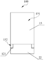
- Figure 1 is a schematic cross-sectional view of a liquid crystal panel of the present invention
- Figure 2 is a top plan view of the liquid crystal panel of the present invention shown in Figure 1;
- FIG. 3 is a top plan view of a liquid crystal panel according to another embodiment of the present invention.
- FIG. 1 is a schematic cross-sectional view showing a liquid crystal panel of the present invention
- FIG. 2 is a schematic plan view showing a liquid crystal panel of the present invention
- the liquid crystal panel 100 mainly includes a color film substrate 11 and an array substrate 12.
- the color filter substrate 11 and the array substrate 12 are disposed opposite each other, and the color filter substrate 11 and the array substrate 12 are bonded into a box-like structure by the sealant 13 .
- the liquid crystal 14 is sealed in the box-like structure.
- the color filter substrate 11 is provided with a polarizer 15 on a side facing away from the array substrate 12.
- the sheet 15 includes a main body 151 and an extending portion 152, and a side of the polarizing plate 15 adjacent to the color filter substrate 11 is covered with a transparent conductive paste 16.
- the main body 151 of the polarizer is attached to the side of the color filter substrate 11 facing away from the array substrate 12 by a transparent conductive adhesive 16, and the main body 151 is disposed opposite to the color filter substrate 11, and the extending portion 152 is extended.
- the array substrate 12 is provided with a grounding point 121, and the extending portion 152 is adhered to the grounding point 121 by a transparent conductive adhesive 16.
- the polarizer 15 conducts static electricity to the transparent conductive paste 16 and discharges the static electricity on the polarizer 15 through the transparent conductive paste under the extending portion 152.
- the polarizer 15 is kept at a potential of zero. That is, when static electricity is generated on the surface of the liquid crystal panel 100, the polarizer 15 connected to the grounding point 121 can pull the static electricity on the surface of the liquid crystal panel 100 to a zero potential, so that the static charge passes through the polarizer 15 and the transparent conductive adhesive 16 .
- the path formed between the ground point 121 discharges static electricity.
- the number of the extensions 152 may be two, and the two extensions 152 are respectively disposed on two sides of the polarizer 15 and on the array substrate 12 .
- the two grounding points 121 are connected with respect to each other.
- the number of the extensions 152 may also be two or more, and the number of the grounding points 121 on the array substrate 12 should also be correspondingly increased. The greater the number of extensions 152, the faster the rate at which static electricity is drawn.
- the extension portion of the polarizer is bonded to the ground point on the array substrate by the transparent conductive paste, so that The static electricity on the polarizer can be released through the polarizer through the transparent conductive paste to the ground point.
- the use of a common polarizer instead of the conductive polarizer of the prior art can effectively reduce the production cost, and then the transparent conductive paste is adhered to the grounding point instead of the conductive silver paste to simplify the manufacturing process, improve the grounding stability, and reduce the production cost.
- the extending portion 151 of the polarizer 15 can be disposed in a corner region around the liquid crystal panel.
- the extension portion 151 should be disposed at a corner region of the polarizer 15. That is, the edge of the extending portion 151 coincides with two intersecting sides on the color filter substrate. This makes it easier to release external static electricity, thereby minimizing the influence of static electricity on the liquid crystal panel.
- the transparent conductive paste 16 can be formed by adding conductive particles to the transparent adhesive layer.
- the transparent conductive adhesive 16 may be made of a material such as acrylic rubber and nickel powder.
- the transparent conductive adhesive 16 may also be made of Indium Tin Oxide (ITO) or antimony doped Tin Oxide. , ATO), Indium Zinc Oxide (IZO), Aluminium Zinc Oxide (AZO), or other metals and metal oxides.
- the selected material may be such that the transparent conductive paste 16 is a transparent conductive layer to increase the transmittance of light.
- the transparent conductive pastes 16 of different thicknesses have different electrical conductivity properties. Generally, the greater the thickness of the transparent conductive adhesive 16, the better the electrical conductivity, but the transmittance of the transparent conductive adhesive 16 will decrease correspondingly under the same conditions; and the smaller the thickness of the transparent conductive adhesive 16, the worse the electrical conductivity, but The light transmittance of the transparent conductive paste 16 is improved under the same conditions.
- the increase in the thickness of the transparent conductive paste 16 also leads to an increase in manufacturing cost. Therefore, the conductive layer 4 needs to have a suitable thickness to trade off its electrical conductivity and light transmittance, so that the transparent conductive paste 16 has both good electrical conductivity and large light transmittance.
- the transparent conductive paste 16 has a thickness of from 0.01 mm to 0.1 mm, more preferably 0.05 mm. When the thickness of the transparent conductive paste 16 is 0.05 mm, the cost is relatively low.
- the transparent conductive paste 16 has a suitable resistance value. In general, it should be ensured that the resistance of the conductive layer per square inch should be less than or equal to 0.02 ⁇ .
- the light transmittance of the conductive layer 4 should be guaranteed to be between 30% and 80%.
- the transparent conductive paste 16 may be coated on the polarizer 15 by spin coating.
- an ESD (Electrical-static-discharge) wiring (not shown) is formed on the upper surface of the array substrate 12.
- a grounding point 121 is provided in the wiring.
- the ESD wiring surrounds the periphery of the array substrate, and at least one end of the ground trace is connected to a pin on the flexible circuit board lead for inputting a ground signal.
- the ESD wiring can be connected to a ground point on the flexible wiring board via a driver IC (Driver IC). Therefore, the grounding signal of the whole system can be connected to the grounding wire inside the panel through the flexible circuit board lead by the principle of electrostatic shielding, and the electrostatic shielding can be realized through the grounding wire, thereby improving the whole
- the antistatic ability of the array substrate can further improve the antistatic capability of the liquid crystal panel.
- the ESD wiring may use a metal material such as Mo or Cr.
- the invention also provides a method for fabricating a liquid crystal panel, which mainly comprises the following steps:
- a liquid crystal panel body includes a color film substrate and an array substrate which are disposed in a stack, the array substrate includes an edge region located opposite to the outside of the color filter substrate, and a grounding point is disposed in the edge region;
- a polarizer that differs from a conventional polarizer in that an extension extends from the body in addition to the body, and a transparent conductive paste is covered on the body and the extension, the body Attaching the transparent conductive adhesive to the color filter substrate, away from the side of the array substrate, the extending portion protrudes from the edge of the main body to the color filter substrate;
- the extension is bonded to the ground point by the transparent conductive paste to form a discharge loop between the ground point and the body.
- the present invention also provides a liquid crystal display comprising the liquid crystal panel of any of the above.
- the present invention also provides an electronic device using the above liquid crystal display, which may be any electronic device having a display function, such as a mobile phone, a tablet computer, a television, a display, a notebook computer, a digital photo frame, a navigator, and the like.
- a display function such as a mobile phone, a tablet computer, a television, a display, a notebook computer, a digital photo frame, a navigator, and the like.
Landscapes
- Physics & Mathematics (AREA)
- Nonlinear Science (AREA)
- Mathematical Physics (AREA)
- Chemical & Material Sciences (AREA)
- Crystallography & Structural Chemistry (AREA)
- General Physics & Mathematics (AREA)
- Optics & Photonics (AREA)
- Engineering & Computer Science (AREA)
- Microelectronics & Electronic Packaging (AREA)
- Liquid Crystal (AREA)
- Polarising Elements (AREA)
Abstract
Description
本发明要求2015年12月9日递交的发明名称为“液晶显示器、电子设备、液晶面板及其制作方法”的申请号201510903533.5的在先申请优先权,上述在先申请的内容以引入的方式并入本文本中。The present invention claims the priority of the application No. 201510903533.5, entitled "Liquid Crystal Display, Electronic Device, Liquid Crystal Panel, and Method of Making the Same," filed on Dec. 9, 2015, the content of which is incorporated herein by reference. Into this text.
本发明涉及液晶显示技术领域,尤其涉及一种具有抗静电结构的液晶显示器。The present invention relates to the field of liquid crystal display technology, and in particular, to a liquid crystal display having an antistatic structure.
随着电子产业日益发达,移动电话(Mobile Phone)、个人数字助理(Personal Digital Assistant)、笔记型计算机(Notebook)及平板型计算机(Planet Computer)等数字化工具无不朝向更便利、多功能且美观的方向发展。然而,移动电话、个人数字助理、笔记型计算机及平板型计算机中的显示屏幕是不可或缺的人机沟通界面,薄膜晶体管-液晶显示器(TFT-LCD)因其画面品质高、功耗低、辐射小、轻薄便携等优点已广泛应用于3D电视、笔记本电脑、iPad、数码相机、iPhone等电子产品,而液晶面板又是整个液晶显示器最为核心的部件。As the electronics industry grows, digital tools such as Mobile Phones, Personal Digital Assistants, Notebooks, and Tablet Computers are all more convenient, versatile, and aesthetically pleasing. Direction development. However, display screens in mobile phones, personal digital assistants, notebook computers, and tablet computers are indispensable human-machine communication interfaces. Thin-film transistor-liquid crystal display (TFT-LCD) has high picture quality and low power consumption. The advantages of small radiation, light and thin portable have been widely used in 3D TV, notebook computer, iPad, digital camera, iPhone and other electronic products, and the liquid crystal panel is the core component of the entire liquid crystal display.
现有Full in cell液晶面板包括:彩膜基板、阵列基板,彩膜基板和阵列基板之间还设有液晶和封框胶等,液晶面板使用过程中在彩膜基板上会产生静电,并传导给偏光片。因此,通常会采用具有导电性的偏光片贴于CF玻璃表面,然后再通过滴导电银浆连接具有导电性的偏光片和TFT基板上的接地点(Ground)连,从而将偏光片上的静电导出。然而,导电偏光片成本比普通的偏光片价格高,滴导电银浆的制程复杂且成本较高,因此制造成本居高不下。此外,导电银浆贴附的稳定性不好,容易断开造成地整个回路断路,严重影响了液晶面板的生产良率和显像品质。The existing Full in cell liquid crystal panel comprises: a color film substrate, an array substrate, a liquid crystal film and a frame sealing glue are also disposed between the color film substrate and the array substrate, and static electricity is generated on the color film substrate during use of the liquid crystal panel, and is conducted. Give a polarizer. Therefore, a conductive polarizer is usually applied to the surface of the CF glass, and then the conductive polarizer is connected to the grounding point on the TFT substrate by the conductive silver paste, thereby discharging the static electricity on the polarizer. . However, the cost of the conductive polarizer is higher than that of the ordinary polarizer, and the process of dropping the conductive silver paste is complicated and the cost is high, so the manufacturing cost is high. In addition, the stability of the conductive silver paste attached is not good, and the entire circuit is easily broken due to disconnection, which seriously affects the production yield and the image quality of the liquid crystal panel.
发明内容Summary of the invention
本发明的目的在于提供一种可以增强偏光片接地的稳定性高、生产成本低 的液晶面板。The object of the present invention is to provide a high stability and low production cost that can enhance the grounding of the polarizer. LCD panel.
本发明的另一目的在于提供一种采用上述液晶面板的液晶显示器。Another object of the present invention is to provide a liquid crystal display using the above liquid crystal panel.
本发明的另一目的在于提供一种采用上述液晶显示器的电子设备。Another object of the present invention is to provide an electronic device using the above liquid crystal display.
本发明的另一目的在于提供一种上述液晶面板的制作方法。Another object of the present invention is to provide a method of fabricating the above liquid crystal panel.
为了实现上述目的,本发明实施方式提供如下技术方案:In order to achieve the above object, the embodiments of the present invention provide the following technical solutions:
本发明提供一种液晶面板,包括阵列基板和与所述阵列基板相对设置的彩膜基板,其中,还包括偏光片,所述偏光片包括主体和延伸部,所述主体和延伸部上覆盖有透明导电胶,所述主体通过所述透明导电胶贴附在所述彩膜基板上远离所述阵列基板的一侧,所述延伸部自所述主体的边缘伸出于所述彩膜基板,所述阵列基板上设有接地点,所述延伸部通过所述透明导电胶与所述接地点粘接,以在所述接地点和所述主体之间形成放电回路。The present invention provides a liquid crystal panel comprising an array substrate and a color filter substrate disposed opposite to the array substrate, further comprising a polarizer, the polarizer comprising a body and an extension, the body and the extension being covered a transparent conductive adhesive, the main body is attached to a side of the color filter substrate away from the array substrate by the transparent conductive adhesive, and the extending portion protrudes from the edge of the main body to the color filter substrate. A grounding point is disposed on the array substrate, and the extending portion is bonded to the grounding point by the transparent conductive adhesive to form a discharge loop between the grounding point and the main body.
其中,所述延伸部设置在所述偏光片的边角区域。Wherein the extension portion is disposed at a corner region of the polarizer.
其中,所述延伸部为两个,两个所述延伸分别设置在所述主体的两个侧边上。Wherein, the extensions are two, and the two extensions are respectively disposed on two sides of the main body.
其中,所述透明导电胶的厚度为0.01mm-0.1mm。Wherein, the transparent conductive adhesive has a thickness of 0.01 mm to 0.1 mm.
其中,所述透明导电胶的透光率为30%-80%。Wherein, the transparent conductive adhesive has a light transmittance of 30% to 80%.
其中,所述透明导电胶每平方英寸的电阻值≤0.02Ω。Wherein, the transparent conductive adhesive has a resistance value per square inch ≤ 0.02 Ω.
其中,所述阵列基板上表面形成有ESD布线,所述接地点与所述ESD布线连接。The upper surface of the array substrate is formed with an ESD wiring, and the ground point is connected to the ESD wiring.
本发明还提供一种液晶显示器,包括液晶面板,所述液晶面板包括阵列基板和与所述阵列基板相对设置的彩膜基板,其中,还包括偏光片,所述偏光片包括主体和延伸部,所述主体和延伸部上覆盖有透明导电胶,所述主体通过所述透明导电胶贴附在所述彩膜基板上远离所述阵列基板的一侧,所述延伸部自所述主体的边缘伸出于所述彩膜基板,所述阵列基板上设有接地点,所述延伸部通过所述透明导电胶与所述接地点粘接,以在所述接地点和所述主体之间形成放电回路。The present invention also provides a liquid crystal display comprising a liquid crystal panel, the liquid crystal panel comprising an array substrate and a color filter substrate disposed opposite to the array substrate, further comprising a polarizer, the polarizer comprising a body and an extension, The main body and the extending portion are covered with a transparent conductive adhesive, and the main body is attached to a side of the color filter substrate away from the array substrate by the transparent conductive adhesive, and the extending portion is from an edge of the main body Extending on the color filter substrate, the array substrate is provided with a grounding point, and the extending portion is adhered to the grounding point by the transparent conductive adhesive to form between the grounding point and the main body Discharge circuit.
其中,所述延伸部设置在所述偏光片的边角区域。Wherein the extension portion is disposed at a corner region of the polarizer.
其中,所述延伸部为两个,两个所述延伸分别设置在所述主体的两个侧边 上。Wherein the extensions are two, and the two extensions are respectively disposed on two sides of the main body on.
其中,所述透明导电胶的厚度为0.01mm-0.1mm。Wherein, the transparent conductive adhesive has a thickness of 0.01 mm to 0.1 mm.
其中,所述透明导电胶的透光率为30%-80%。Wherein, the transparent conductive adhesive has a light transmittance of 30% to 80%.
其中,所述透明导电胶每平方英寸的电阻值≤0.02Ω。Wherein, the transparent conductive adhesive has a resistance value per square inch ≤ 0.02 Ω.
本发明提供一种电子设备,包括液晶显示器,所述液晶显示器包括液晶面板,所述液晶面板包括阵列基板和与所述阵列基板相对设置的彩膜基板,其中,还包括偏光片,所述偏光片包括主体和延伸部,所述主体和延伸部上覆盖有透明导电胶,所述主体通过所述透明导电胶贴附在所述彩膜基板上远离所述阵列基板的一侧,所述延伸部自所述主体的边缘伸出于所述彩膜基板,所述阵列基板上设有接地点,所述延伸部通过所述透明导电胶与所述接地点粘接,以在所述接地点和所述主体之间形成放电回路。The present invention provides an electronic device including a liquid crystal display, the liquid crystal display including a liquid crystal panel, the liquid crystal panel including an array substrate and a color filter substrate disposed opposite to the array substrate, wherein the liquid crystal display further includes a polarizer, the polarized light The sheet includes a main body and an extension portion, the main body and the extension portion are covered with a transparent conductive paste, and the main body is attached to a side of the color filter substrate away from the array substrate by the transparent conductive adhesive, the extension And extending from the edge of the main body to the color filter substrate, wherein the array substrate is provided with a grounding point, and the extending portion is adhered to the grounding point by the transparent conductive adhesive to be at the grounding point A discharge loop is formed between the body and the body.
其中,所述延伸部设置在所述偏光片的边角区域。Wherein the extension portion is disposed at a corner region of the polarizer.
其中,所述延伸部为两个,两个所述延伸分别设置在所述主体的两个侧边上。Wherein, the extensions are two, and the two extensions are respectively disposed on two sides of the main body.
其中,所述透明导电胶的厚度为0.01mm-0.1mm。Wherein, the transparent conductive adhesive has a thickness of 0.01 mm to 0.1 mm.
其中,所述透明导电胶的透光率为30%-80%。Wherein, the transparent conductive adhesive has a light transmittance of 30% to 80%.
其中,所述透明导电胶每平方英寸的电阻值≤0.02Ω。Wherein, the transparent conductive adhesive has a resistance value per square inch ≤ 0.02 Ω.
本发明提供一种液晶面板制作方法,其中,包括如下步骤:The invention provides a method for fabricating a liquid crystal panel, which comprises the following steps:
提供一液晶面板主体,所述液晶面板主体包括层叠设置的彩膜基板和阵列基板,所述阵列基板包括相对位于所述彩膜基板外部的边缘区域,所述边缘区域内设接地点;Providing a liquid crystal panel body, the liquid crystal panel body comprising a color film substrate and an array substrate disposed in a stack, the array substrate includes an edge region opposite to the outside of the color filter substrate, and a grounding point is disposed in the edge region;
提供一包括主体和延伸部的偏光片,在所述主体和所述延伸部覆盖一层透明导电胶;Providing a polarizer comprising a body and an extension, wherein the body and the extension are covered with a layer of transparent conductive adhesive;
将所述主体通过所述透明导电胶贴合至所述彩膜基板之远离所述阵列基板的一侧,所述延伸部自所述主体的边缘伸出于所述彩膜基板;Bonding the main body to the side of the color filter substrate away from the array substrate through the transparent conductive adhesive, the extending portion protruding from the edge of the main body to the color filter substrate;
将所述延伸部通过所述透明导电胶与所述接地点粘接,以在所述接地点和所述主体之间形成放电回路。The extension is bonded to the ground point by the transparent conductive paste to form a discharge loop between the ground point and the body.
本发明实施例具有如下优点或有益效果: Embodiments of the present invention have the following advantages or benefits:
本发明中,通过在偏光片与彩膜基板之间设置透明导电胶,偏光片延伸出延伸部,延伸部通过透明导电胶粘结到阵列基板上的接地点的方法,使得在偏光片上的静电可以通过偏光片经透明导电胶传导到接地点释放。使用普通偏光片代替现有技术中的导电偏光片可以有效降低生产成本,再通过透明导电胶将延伸部粘贴在接地点代替导电银浆可以达到简化制作工艺、提高接地稳定性、降低生产成本的技术效果。In the present invention, by providing a transparent conductive paste between the polarizer and the color filter substrate, the polarizer extends out of the extension portion, and the extension portion is bonded to the grounding point on the array substrate through the transparent conductive adhesive, so that the static electricity on the polarizer It can be released through the polarizer through the transparent conductive adhesive to the ground point. The use of a common polarizer instead of the conductive polarizer of the prior art can effectively reduce the production cost, and then the transparent conductive paste is adhered to the grounding point instead of the conductive silver paste to simplify the manufacturing process, improve the grounding stability, and reduce the production cost. Technical effects.
为了更清楚地说明本发明实施例或现有技术中的技术方案,下面将对实施例或现有技术描述中所需要使用的附图作简单地介绍,显而易见地,下面描述中的附图仅仅是本发明的一些实施例,对于本领域普通技术人员来讲,在不付出创造性劳动的前提下,还可以根据这些附图获得其他的附图。In order to more clearly illustrate the embodiments of the present invention or the technical solutions in the prior art, the drawings used in the embodiments or the description of the prior art will be briefly described below. Obviously, the drawings in the following description are only It is a certain embodiment of the present invention, and other drawings can be obtained from those skilled in the art without any creative work.
图1是本发明的液晶面板的剖面示意图;Figure 1 is a schematic cross-sectional view of a liquid crystal panel of the present invention;
图2是图1所述本发明的液晶面板的俯视示意图;Figure 2 is a top plan view of the liquid crystal panel of the present invention shown in Figure 1;
图3是本发明另一实施例的液晶面板的俯视示意图。3 is a top plan view of a liquid crystal panel according to another embodiment of the present invention.
下面将结合本发明实施例中的附图,对本发明实施例中的技术方案进行清楚、完整地描述,显然,所描述的实施例仅仅是本发明一部分实施例,而不是全部的实施例。基于本发明中的实施例,本领域普通技术人员在没有做出创造性劳动前提下所获得的所有其他实施例,都属于本发明保护的范围。The technical solutions in the embodiments of the present invention are clearly and completely described in the following with reference to the accompanying drawings in the embodiments of the present invention. It is obvious that the described embodiments are only a part of the embodiments of the present invention, but not all embodiments. All other embodiments obtained by those skilled in the art based on the embodiments of the present invention without creative efforts are within the scope of the present invention.
请参阅图1、图2,图1表示本发明的液晶面板的剖面示意图,图2表示本发明的液晶面板的俯视示意图。液晶面板100主要包括一彩膜基板11和一阵列基板12。彩膜基板11和阵列基板12相对设置,并通过封框胶13将彩膜基板11和阵列基板12粘合成盒状结构。液晶14被密封在所述盒状结构中。所述彩膜基板11在背离所述阵列基板12的一侧上设有偏光片15。所述偏光
片15包括主体151和延伸部152,所述偏光片15靠近所述彩膜基板11的一侧覆盖有透明导电胶16。所述偏光片的主体151通过透明导电胶16贴附在所述彩膜基板11背离所述阵列基板12一侧,所述主体151与所述彩膜基板11相对设置,所述延伸部152伸出于所述彩膜基板11。所述阵列基板12上设有接地点121,所述延伸部152通过透明导电胶16粘接在所述接地点121上。所述偏光片15将静电传导到透明导电胶16上,并通过延伸部152下方的透明导电胶将偏光片15上的静电导出。使偏光片15保持零电位。也就是说,当该液晶面板100表面有静电产生时,与接地点121连接的偏光片15可以将液晶面板100表面的静电拉至零电位,使静电荷经过该偏光片15、透明导电胶16与接地点121之间形成的通路释放静电。1 and 2, FIG. 1 is a schematic cross-sectional view showing a liquid crystal panel of the present invention, and FIG. 2 is a schematic plan view showing a liquid crystal panel of the present invention. The
请参阅图3,本发明的另一实施例中,延伸部152的数量可以为两个,两个所述延伸部152分别设置在偏光片15的两个侧边上,并且与阵列基板12上相对于的两个接地点121相连接。显而易见的,延伸部152的数量还可以为两个以上,此时阵列基板12上接地点121的数量也应相应增加。所述延伸部152的数量越多,其导出静电的速度越快。Referring to FIG. 3 , in another embodiment of the present invention, the number of the
本发明中,通过在偏光片与彩膜基板之间设置透明导电胶,且偏光片延伸出延伸部,偏光片的延伸部通过透明导电胶粘结到阵列基板上的接地点的方法,使得在偏光片上的静电可以通过偏光片经透明导电胶传导到接地点释放。使用普通偏光片代替现有技术中的导电偏光片可以有效降低生产成本,再通过透明导电胶将延伸部粘贴在接地点代替导电银浆可以达到简化制作工艺、提高接地稳定性、降低生产成本的技术效果。In the present invention, by providing a transparent conductive paste between the polarizer and the color filter substrate, and the polarizer extends out of the extension portion, the extension portion of the polarizer is bonded to the ground point on the array substrate by the transparent conductive paste, so that The static electricity on the polarizer can be released through the polarizer through the transparent conductive paste to the ground point. The use of a common polarizer instead of the conductive polarizer of the prior art can effectively reduce the production cost, and then the transparent conductive paste is adhered to the grounding point instead of the conductive silver paste to simplify the manufacturing process, improve the grounding stability, and reduce the production cost. Technical effects.
进一步的,由于电荷的分布一般满足曲率大的地方电荷密度大,曲率小的地方电荷密度小,所以液晶面板的边角等尖锐区域是静电易放电的区域。因此,偏光片15的延伸部151可以设置在液晶面板四周的边角区域。换而言之,所述延伸部151应设置在所述偏光片15的边角区域。也就是说,所述延伸部151的边缘与所述彩膜基板上两条相交的边重合。这样比较容易将外界的静电进行释放,从而最大程度地降低液晶面板受静电的影响。
Further, since the charge distribution generally satisfies a large charge density in a place having a large curvature and a small charge density in a place where a curvature is small, a sharp region such as a corner of the liquid crystal panel is a region in which the static electricity is easily discharged. Therefore, the extending
更进一步的,所述透明导电胶16可以通过在透明胶层中添加导电颗粒形成。进一步优选的,透明导电胶16可以采用诸如亚克力胶和镍粉为主要材料,当然此透明导电胶16的材料还可以采用氧化铟锡(Indium Tin Oxide,ITO)、氧化锡锑(Antimony Doped Tin Oxide,ATO)、氧化铟锌(Indium Zinc Oxide,IZO)、氧化锌铝(Aluminum ZincOxide,AZO)等制作,或是采用其它金属及金属氧化物制作。进一步优选的,选择的材料可以使透明导电胶16为透明导电层,以增加光线的透过率。Further, the transparent
更进一步的,不同厚度的透明导电胶16具有不同的导电性能。一般来说,透明导电胶16的厚度越大,导电性能越好,但相同条件下透明导电胶16的透光率会相应下降;而透明导电胶16的厚度越小,导电性能越差,但相同条件下透明导电胶16的透光率会有所提高。此外,透明导电胶16的厚度提升,也会带来制作成本的上升。因此,导电层4需要具有合适的厚度以对其导电性能和透光率进行折衷,使透明导电胶16既有良好的导电性又有较大的透光率。优选的,透明导电胶16的厚度为0.01mm-0.1mm,更优选的为0.05mm。透明导电胶16的厚度为0.05mm时的造价相对来说也比较低廉。Further, the transparent
进一步的,应当保证透明导电胶16具有合适电阻值。一般情况下,应当保证每平方英寸的导电层电阻值应当小于等于0.02Ω。Further, it should be ensured that the transparent
更进一步的,导电层4的透光率应当保证在30%-80%之间。Further, the light transmittance of the conductive layer 4 should be guaranteed to be between 30% and 80%.
更进一步的,本发明中可以采用旋涂法将透明导电胶16涂覆在所述偏光片15上。Further, in the present invention, the transparent
进一步的,在阵列基板12上表面形成有ESD(Electrical-static-discharge,静电放电)布线(图未示出)。在布线中设有接地点121。ESD布线环绕阵列基板周边,并且该接地走线的至少一端与所述柔性线路板引线上用于输入接地信号的管脚相连。Further, an ESD (Electrical-static-discharge) wiring (not shown) is formed on the upper surface of the
进一步的,ESD布线可以经由驱动电路(Driver IC)连至柔性线路板上的接地点。从而可以利用静电屏蔽的原理,将整机系统的接地信号通过柔性线路板引线接入到面板内部的接地走线,通过接地走线实现静电屏蔽,提高了整个 阵列基板的抗静电能力,进而可以提高液晶面板的抗静电能力。Further, the ESD wiring can be connected to a ground point on the flexible wiring board via a driver IC (Driver IC). Therefore, the grounding signal of the whole system can be connected to the grounding wire inside the panel through the flexible circuit board lead by the principle of electrostatic shielding, and the electrostatic shielding can be realized through the grounding wire, thereby improving the whole The antistatic ability of the array substrate can further improve the antistatic capability of the liquid crystal panel.
优选的,所述ESD布线可以使用Mo、Cr等金属材料。Preferably, the ESD wiring may use a metal material such as Mo or Cr.
本发明还提供了一种液晶面板制作方法,主要包括如下步骤:The invention also provides a method for fabricating a liquid crystal panel, which mainly comprises the following steps:
首先,提供一液晶面板主体,所述液晶面板主体包括层叠设置的彩膜基板和阵列基板,所述阵列基板包括相对位于所述彩膜基板外部的边缘区域,所述边缘区域内设接地点;First, a liquid crystal panel body is provided, the liquid crystal panel body includes a color film substrate and an array substrate which are disposed in a stack, the array substrate includes an edge region located opposite to the outside of the color filter substrate, and a grounding point is disposed in the edge region;
提供一个偏光片,所述偏光片与普通偏光片的区别在于,除了主体外还在所述主体延伸出延伸部,并在所述主体和所述延伸部覆盖一层透明导电胶,所述主体通过所述透明导电胶与所述彩膜基板贴合,之远离所述阵列基板的一侧,所述延伸部自所述主体的边缘伸出于所述彩膜基板;Providing a polarizer that differs from a conventional polarizer in that an extension extends from the body in addition to the body, and a transparent conductive paste is covered on the body and the extension, the body Attaching the transparent conductive adhesive to the color filter substrate, away from the side of the array substrate, the extending portion protrudes from the edge of the main body to the color filter substrate;
最后,所述延伸部通过所述透明导电胶与所述接地点粘接,以在所述接地点和所述主体之间形成放电回路。Finally, the extension is bonded to the ground point by the transparent conductive paste to form a discharge loop between the ground point and the body.
本发明还提供了一种液晶显示器,本发明的液晶显示器包括上述的任意一种液晶面板。The present invention also provides a liquid crystal display comprising the liquid crystal panel of any of the above.
本发明还提供一种采用上述液晶显示器的电子设备,所述电子设备可以是手机、平板电脑、电视机、显示器、笔记本电脑、数码相框、导航仪等任何具有显示功能的电子设备。The present invention also provides an electronic device using the above liquid crystal display, which may be any electronic device having a display function, such as a mobile phone, a tablet computer, a television, a display, a notebook computer, a digital photo frame, a navigator, and the like.
以上所述的实施方式,并不构成对该技术方案保护范围的限定。任何在上述实施方式的精神和原则之内所作的修改、等同替换和改进等,均应包含在该技术方案的保护范围之内。 The embodiments described above do not constitute a limitation on the scope of protection of the technical solutions. Any modifications, equivalent substitutions and improvements made within the spirit and principles of the above-described embodiments are intended to be included within the scope of the technical solutions.
Claims (20)
Priority Applications (1)
| Application Number | Priority Date | Filing Date | Title |
|---|---|---|---|
| US14/906,550 US9841647B2 (en) | 2015-12-09 | 2015-12-30 | Liquid crystal display, electronic device and liquid crystal panel |
Applications Claiming Priority (2)
| Application Number | Priority Date | Filing Date | Title |
|---|---|---|---|
| CN201510903533.5 | 2015-12-09 | ||
| CN201510903533.5A CN105319767A (en) | 2015-12-09 | 2015-12-09 | Liquid crystal displayer, electronic device, liquid crystal panel and manufacturing method thereof |
Publications (1)
| Publication Number | Publication Date |
|---|---|
| WO2017096666A1 true WO2017096666A1 (en) | 2017-06-15 |
Family
ID=55247501
Family Applications (1)
| Application Number | Title | Priority Date | Filing Date |
|---|---|---|---|
| PCT/CN2015/099782 Ceased WO2017096666A1 (en) | 2015-12-09 | 2015-12-30 | Liquid crystal display, electronic device, liquid crystal panel and manufacturing method therefor |
Country Status (3)
| Country | Link |
|---|---|
| US (1) | US9841647B2 (en) |
| CN (1) | CN105319767A (en) |
| WO (1) | WO2017096666A1 (en) |
Cited By (1)
| Publication number | Priority date | Publication date | Assignee | Title |
|---|---|---|---|---|
| CN111190301A (en) * | 2020-02-27 | 2020-05-22 | 厦门天马微电子有限公司 | Display panel and display device |
Families Citing this family (17)
| Publication number | Priority date | Publication date | Assignee | Title |
|---|---|---|---|---|
| CN105717710B (en) * | 2016-04-05 | 2019-01-08 | 友达光电(昆山)有限公司 | A kind of display panel and its manufacturing method |
| CN105929478A (en) * | 2016-06-29 | 2016-09-07 | 京东方科技集团股份有限公司 | Polaroid, manufacture method of Polaroid, display panel, manufacture method of display panel, display apparatus and manufacture method of display apparatus |
| CN106547406B (en) * | 2016-11-04 | 2019-12-20 | 昆山龙腾光电有限公司 | Assembling method of touch display module |
| CN106531096B (en) * | 2016-11-28 | 2019-12-24 | 武汉华星光电技术有限公司 | RGBW four primary color display panel driving method |
| CN108279456B (en) * | 2017-01-05 | 2024-03-15 | 京东方科技集团股份有限公司 | Polarizers, color film substrates, display panels and display equipment |
| CN106547135B (en) * | 2017-01-23 | 2019-12-31 | 武汉华星光电技术有限公司 | Glue material and preparation method thereof, liquid crystal module manufacturing method and liquid crystal module |
| CN107065287B (en) * | 2017-05-24 | 2021-03-02 | 厦门天马微电子有限公司 | Display panel and display device |
| CN108776407B (en) * | 2018-05-31 | 2021-08-27 | 信利光电股份有限公司 | Display module and terminal |
| CN109116608B (en) * | 2018-09-14 | 2022-03-25 | Oppo(重庆)智能科技有限公司 | Display screen, manufacturing method of display screen and electronic equipment |
| CN109116622A (en) * | 2018-09-30 | 2019-01-01 | 上海天马微电子有限公司 | Display panel and display device |
| CN108931867B (en) * | 2018-10-19 | 2024-03-12 | 信利光电股份有限公司 | Liquid crystal display module |
| CN109061930B (en) * | 2018-11-06 | 2021-06-18 | 上海天马微电子有限公司 | Display panel and display device |
| CN110031993A (en) * | 2019-04-18 | 2019-07-19 | 上海摩软通讯技术有限公司 | A kind of display panel and display device |
| CN110515232A (en) * | 2019-09-02 | 2019-11-29 | 联想(北京)有限公司 | Display panel, display module, electronic equipment and display panel preparation method |
| CN110517584B (en) * | 2019-09-02 | 2022-02-01 | 京东方科技集团股份有限公司 | Display module, display device and preparation method of display module |
| CN110908197A (en) * | 2019-11-08 | 2020-03-24 | 武汉华星光电技术有限公司 | Liquid crystal display panel and display device |
| CN110989238A (en) * | 2019-12-12 | 2020-04-10 | 武汉华星光电技术有限公司 | Display panel, display device and manufacturing method of display panel |
Citations (6)
| Publication number | Priority date | Publication date | Assignee | Title |
|---|---|---|---|---|
| US20090033825A1 (en) * | 2007-07-31 | 2009-02-05 | Hitachi Displays, Ltd. | Liquid Crystal Display Device |
| CN202256961U (en) * | 2011-10-26 | 2012-05-30 | 京东方科技集团股份有限公司 | Liquid crystal display device and color film substrate and polarizing sheet thereof |
| US20130002993A1 (en) * | 2011-07-01 | 2013-01-03 | Oh Dae-Kyun | Liquid crystal display |
| CN103969884A (en) * | 2014-04-24 | 2014-08-06 | 京东方科技集团股份有限公司 | Polarizer, substrate structure and display panel |
| CN104536184A (en) * | 2014-12-25 | 2015-04-22 | 上海天马微电子有限公司 | Display panel and display device |
| CN204807871U (en) * | 2015-05-08 | 2015-11-25 | 上海天马微电子有限公司 | Display panel and display device |
Family Cites Families (4)
| Publication number | Priority date | Publication date | Assignee | Title |
|---|---|---|---|---|
| CN101971345B (en) * | 2007-10-29 | 2014-06-25 | 三星电子株式会社 | Nanostructured Thin Film LCD Devices |
| JP5079715B2 (en) * | 2009-01-16 | 2012-11-21 | 株式会社ジャパンディスプレイウェスト | Liquid crystal display |
| TW201042298A (en) * | 2009-05-27 | 2010-12-01 | Chi Mei Optoelectronics Corp | Polarizer, liquid crystal display panel, and liquid crystal display module |
| CN202948225U (en) * | 2012-11-19 | 2013-05-22 | 信利半导体有限公司 | Liquid crystal displayer |
-
2015
- 2015-12-09 CN CN201510903533.5A patent/CN105319767A/en active Pending
- 2015-12-30 US US14/906,550 patent/US9841647B2/en active Active
- 2015-12-30 WO PCT/CN2015/099782 patent/WO2017096666A1/en not_active Ceased
Patent Citations (6)
| Publication number | Priority date | Publication date | Assignee | Title |
|---|---|---|---|---|
| US20090033825A1 (en) * | 2007-07-31 | 2009-02-05 | Hitachi Displays, Ltd. | Liquid Crystal Display Device |
| US20130002993A1 (en) * | 2011-07-01 | 2013-01-03 | Oh Dae-Kyun | Liquid crystal display |
| CN202256961U (en) * | 2011-10-26 | 2012-05-30 | 京东方科技集团股份有限公司 | Liquid crystal display device and color film substrate and polarizing sheet thereof |
| CN103969884A (en) * | 2014-04-24 | 2014-08-06 | 京东方科技集团股份有限公司 | Polarizer, substrate structure and display panel |
| CN104536184A (en) * | 2014-12-25 | 2015-04-22 | 上海天马微电子有限公司 | Display panel and display device |
| CN204807871U (en) * | 2015-05-08 | 2015-11-25 | 上海天马微电子有限公司 | Display panel and display device |
Cited By (2)
| Publication number | Priority date | Publication date | Assignee | Title |
|---|---|---|---|---|
| CN111190301A (en) * | 2020-02-27 | 2020-05-22 | 厦门天马微电子有限公司 | Display panel and display device |
| CN111190301B (en) * | 2020-02-27 | 2022-11-04 | 厦门天马微电子有限公司 | Display panel and display device |
Also Published As
| Publication number | Publication date |
|---|---|
| CN105319767A (en) | 2016-02-10 |
| US20170269442A1 (en) | 2017-09-21 |
| US9841647B2 (en) | 2017-12-12 |
Similar Documents
| Publication | Publication Date | Title |
|---|---|---|
| WO2017096666A1 (en) | Liquid crystal display, electronic device, liquid crystal panel and manufacturing method therefor | |
| CN105319751B (en) | a display device | |
| US10309616B2 (en) | Display panel for releasing static electricity and display device | |
| CN205193761U (en) | Touch display device and electronic equipment | |
| CN105158964B (en) | Liquid crystal display panel, liquid crystal display and electronic equipment | |
| CN102981322A (en) | Horizontal electric field mode liquid crystal display panel and display device | |
| CN106154632A (en) | Display floater and display device | |
| CN103268168B (en) | Touch control display module | |
| WO2018196272A1 (en) | Touch panel, display device, and method for manufacturing touch panel | |
| CN205038423U (en) | Display device | |
| CN108037857A (en) | Touch-control display panel | |
| CN105158937A (en) | Liquid crystal display panel and electronic device | |
| CN106257324B (en) | In-cell touch display device | |
| CN110703477A (en) | Display panel and display device | |
| US20180373091A1 (en) | Display panel | |
| TWI534506B (en) | Display device | |
| CN203490440U (en) | Display device | |
| CN107861656A (en) | Manufacture method, the display device of touch-screen | |
| WO2016192261A1 (en) | Plastic frame assembly, backlight module and display device | |
| CN206020875U (en) | Display floater and display device | |
| US20230087056A1 (en) | Display panel and display device | |
| CN102305974A (en) | Display device and manufacturing method thereof | |
| CN202281885U (en) | Planar electric field type liquid crystal display panel and polaroid | |
| WO2020082494A1 (en) | Display panel and manufacturing method therefor as well as display module | |
| US10061155B2 (en) | Polarizer, display panel and display device |
Legal Events
| Date | Code | Title | Description |
|---|---|---|---|
| WWE | Wipo information: entry into national phase |
Ref document number: 14906550 Country of ref document: US |
|
| 121 | Ep: the epo has been informed by wipo that ep was designated in this application |
Ref document number: 15910140 Country of ref document: EP Kind code of ref document: A1 |
|
| NENP | Non-entry into the national phase |
Ref country code: DE |
|
| 122 | Ep: pct application non-entry in european phase |
Ref document number: 15910140 Country of ref document: EP Kind code of ref document: A1 |