WO2016117541A1 - Void array structure and method for producing same - Google Patents
Void array structure and method for producing same Download PDFInfo
- Publication number
- WO2016117541A1 WO2016117541A1 PCT/JP2016/051405 JP2016051405W WO2016117541A1 WO 2016117541 A1 WO2016117541 A1 WO 2016117541A1 JP 2016051405 W JP2016051405 W JP 2016051405W WO 2016117541 A1 WO2016117541 A1 WO 2016117541A1
- Authority
- WO
- WIPO (PCT)
- Prior art keywords
- main surface
- void
- pattern
- arrangement structure
- gap
- Prior art date
- Legal status (The legal status is an assumption and is not a legal conclusion. Google has not performed a legal analysis and makes no representation as to the accuracy of the status listed.)
- Ceased
Links
Images


Classifications
-
- G—PHYSICS
- G01—MEASURING; TESTING
- G01N—INVESTIGATING OR ANALYSING MATERIALS BY DETERMINING THEIR CHEMICAL OR PHYSICAL PROPERTIES
- G01N1/00—Sampling; Preparing specimens for investigation
- G01N1/28—Preparing specimens for investigation including physical details of (bio-)chemical methods covered elsewhere, e.g. G01N33/50, C12Q
- G01N1/40—Concentrating samples
- G01N1/4077—Concentrating samples by other techniques involving separation of suspended solids
-
- B—PERFORMING OPERATIONS; TRANSPORTING
- B01—PHYSICAL OR CHEMICAL PROCESSES OR APPARATUS IN GENERAL
- B01D—SEPARATION
- B01D29/00—Filters with filtering elements stationary during filtration, e.g. pressure or suction filters, not covered by groups B01D24/00 - B01D27/00; Filtering elements therefor
- B01D29/0093—Making filtering elements not provided for elsewhere
-
- B—PERFORMING OPERATIONS; TRANSPORTING
- B01—PHYSICAL OR CHEMICAL PROCESSES OR APPARATUS IN GENERAL
- B01D—SEPARATION
- B01D29/00—Filters with filtering elements stationary during filtration, e.g. pressure or suction filters, not covered by groups B01D24/00 - B01D27/00; Filtering elements therefor
- B01D29/0095—Flat filtering elements
-
- B—PERFORMING OPERATIONS; TRANSPORTING
- B01—PHYSICAL OR CHEMICAL PROCESSES OR APPARATUS IN GENERAL
- B01D—SEPARATION
- B01D29/00—Filters with filtering elements stationary during filtration, e.g. pressure or suction filters, not covered by groups B01D24/00 - B01D27/00; Filtering elements therefor
- B01D29/50—Filters with filtering elements stationary during filtration, e.g. pressure or suction filters, not covered by groups B01D24/00 - B01D27/00; Filtering elements therefor with multiple filtering elements, characterised by their mutual disposition
- B01D29/56—Filters with filtering elements stationary during filtration, e.g. pressure or suction filters, not covered by groups B01D24/00 - B01D27/00; Filtering elements therefor with multiple filtering elements, characterised by their mutual disposition in series connection
-
- G—PHYSICS
- G01—MEASURING; TESTING
- G01N—INVESTIGATING OR ANALYSING MATERIALS BY DETERMINING THEIR CHEMICAL OR PHYSICAL PROPERTIES
- G01N21/00—Investigating or analysing materials by the use of optical means, i.e. using sub-millimetre waves, infrared, visible or ultraviolet light
- G01N21/17—Systems in which incident light is modified in accordance with the properties of the material investigated
- G01N21/25—Colour; Spectral properties, i.e. comparison of effect of material on the light at two or more different wavelengths or wavelength bands
- G01N21/31—Investigating relative effect of material at wavelengths characteristic of specific elements or molecules, e.g. atomic absorption spectrometry
- G01N21/35—Investigating relative effect of material at wavelengths characteristic of specific elements or molecules, e.g. atomic absorption spectrometry using infrared light
- G01N21/3581—Investigating relative effect of material at wavelengths characteristic of specific elements or molecules, e.g. atomic absorption spectrometry using infrared light using far infrared light; using Terahertz radiation
-
- G—PHYSICS
- G01—MEASURING; TESTING
- G01N—INVESTIGATING OR ANALYSING MATERIALS BY DETERMINING THEIR CHEMICAL OR PHYSICAL PROPERTIES
- G01N1/00—Sampling; Preparing specimens for investigation
- G01N1/28—Preparing specimens for investigation including physical details of (bio-)chemical methods covered elsewhere, e.g. G01N33/50, C12Q
- G01N1/40—Concentrating samples
- G01N1/4077—Concentrating samples by other techniques involving separation of suspended solids
- G01N2001/4088—Concentrating samples by other techniques involving separation of suspended solids filtration
Definitions
- the object in the sample is collected in the void arrangement structure using a void arrangement structure having a plurality of holes as a filter.
- a method of using a void-arranged structure in which an object is collected for measurement is known.
- the target object is a minute object contained in a fluid (specimen) such as PM2.5 existing in the atmosphere or an endoplasmic reticulum contained in blood
- a porous (mesh-like) structure having pores smaller than those of the object is required.
- Patent Document 1 International Publication No. 2014/064410
- FIG. 8 and Patent Document 2 Japanese Utility Model Laid-Open Publication No. 59-10879
- voids there are two through holes (voids).
- a void arrangement structure in which one void arrangement structure is laminated so that one of the void portions of one void arrangement structure partially overlaps only one of the void portions of the other void arrangement structure. Has been. By producing the filter in this way, a filter having a minute gap can be produced relatively easily.
- Patent Document 3 Japanese Patent Laid-Open No. 2010-42349
- Patent Document 4 Japanese Patent Laid-Open No. 11-276820
- a filter gap disposition structure in which a smaller mesh is formed by laminating a plurality of mesh structures so that the positions of the meshes are shifted from each other is disclosed. Yes.
- the thickness of the void-arranged structure is preferably thin as long as the necessary mechanical strength can be maintained.
- the thickness of the gap-arranged structure when it is used as a filter, generally, the pressure loss when a fluid is passed increases. This is because when the pressure loss of the gap-arranged structure increases, the flow rate becomes slow and it becomes difficult to flow the fluid, so that there is a problem that the processing efficiency is lowered.
- the thickness of the gap arrangement structure when it is used as a measurement device, the influence due to adhesion of the target object (measurement object) is reduced, resulting in a problem that measurement sensitivity is lowered.
- the gap arrangement structure disclosed in Patent Documents 1 and 2 requires the thickness of the two-layer gap arrangement structure, the entire thickness is increased. Furthermore, in the gap arrangement structures disclosed in Patent Documents 3 and 4, in order to form a mesh smaller than a mesh composed of two layers of wire rods arranged in parallel, at least four wire rod groups Need to be laminated. Therefore, the gap arrangement structures disclosed in Patent Documents 3 and 4 are further increased in thickness.
- an object of the present invention is to provide a void-arranged structure that has a small void portion and is thin and has sufficient strength, and a method for manufacturing the void-arranged structure.
- a film-like first pattern having a plurality of first voids penetrating in the normal direction of the first main surface and a plurality of second voids penetrating in the normal direction of the first main surface. And having a shape formed by superimposing the film-like second pattern on the first main surface,
- Each of the plurality of first gaps overlaps three or more of the plurality of second gaps in a plan view as viewed from the normal direction of the first main surface, and the plurality of second gaps
- Each of the portions overlaps three or more of the plurality of first gap portions,
- the gap is an overlapping portion of the plurality of first gaps and the plurality of second gaps,
- the first pattern and the second pattern have the same shape,
- the first structure is formed by lithography using a first resist, and then the first resist is removed.
- the present invention it is possible to provide a void-arranged structure having a small gap and having a small thickness and sufficient strength, and a manufacturing method thereof.
- FIG. 3 is a plan view showing the structure of the void arrangement structure according to the first embodiment. It is a schematic diagram for demonstrating a structure of the space
- FIG. (A) is a perspective view
- (b) is a plan view.
- (A) is a top view which shows the structure of the modification of the space
- FIG. (B) is a top view which shows the structure of another modification of the space
- FIG. 6 is a schematic diagram illustrating a structure of a void arrangement structure according to Embodiment 2.
- FIG. (A) is a top view
- (b) is a perspective view.
- FIG. 10 is a plan view showing a structure of a modified example of the gap arrangement structure according to Embodiment 2.
- FIG. 10 is a plan view showing a structure of another modified example of the gap arrangement structure according to Embodiment 2.
- FIG. 10 is a cross-sectional view for explaining a method for manufacturing the void arrangement structure according to the second embodiment. It is a graph which shows the relationship between the thickness of a space
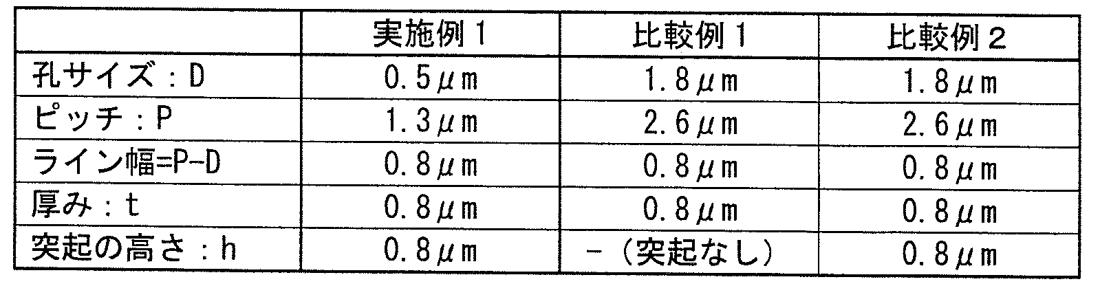
- (A) shows the unit structure of Example 1
- (b) shows the unit structure of Comparative Example 1
- (c) shows the unit structure of Comparative Example 2.
- permeability spectrum which shows the simulation result for demonstrating the effect at the time of using the space
- (A) shows the results of Example 1
- (b) shows the results of Comparative Example 1
- (c) shows the results of Comparative Example 2.
- the gap arrangement structure 1 of the present embodiment basically has a pair of main surfaces (a first main surface 1a and a second main surface 1b) facing each other as shown in FIG. A film-like structure having a plurality of voids 1c penetrating the first main surface 1a and the second main surface 1b.
- gap arrangement structure body 1 of this embodiment is a partial area
- the normal direction of the first main surface 1a protrudes from the second main surface 1b. It has the permite
- the area where the protrusion is provided is an area in contact with three or more gap portions (intersection portion of the crosspieces). Therefore, the portion where the stress is applied is reinforced, and the strength of the void arrangement structure is improved. Therefore, the gap arrangement structure according to the present embodiment can maintain sufficient strength even if the thickness is reduced.
- FIG. 1 and the like of International Publication No. 2012/29629 in the unit structure constituting the void arrangement structure (periodic structure), in the region in contact with the two voids (in the middle of the crosspiece), A void arrangement structure having a protrusion protruding in a direction perpendicular to the surface is disclosed.
- this protrusion is not provided in a region in contact with three or more gaps, and this region where stress is applied from three or more directions cannot be reinforced.
- the plurality of gaps 1c are periodically arranged in a horizontal direction on the first main surface 1a (second main surface 1b).
- all of the gaps 1c may be periodically arranged, and within a range that does not impair the effects of the present invention, some of the gaps 1c are periodically arranged and other gaps 1c are non- You may arrange
- each of the plurality of first gap portions 11c is 4 in a plan view as viewed from the normal direction of the first main surface 1a (second main surface 1b). It is designed so that it overlaps with the two second gaps 12c and each of the plurality of second gaps 12c overlaps with the four first gaps 11c. Thereby, a portion where the plurality of first gap portions 11 c and the plurality of second gap portions 12 c overlap with each other becomes the gap portion 1 c of the gap arrangement structure 1.
- the second resist 42 is removed by a peeling method.
- the metal film 3 is removed by etching.
- the etching method include a method in which the precursor of the void-arranged structure obtained in the above step is immersed in an etching solution that dissolves the metal film. Note that the etching solution is washed by, for example, rinsing with pure water, and then dried.
- the void arrangement structure 1 according to the present embodiment including the first structure 110 and the second structure 120 can be obtained.
- the size of the void is smaller than the void (first void 11c) of the first pattern 11 and the void (second void 12c) of the second pattern 12.
- the gap 1c can be formed. For this reason, it is only necessary to form the first structure body 110 and the second structure body 120 having a gap portion having a size larger than the gap portion 1c, and the fine gap portion 1c can be produced relatively easily.
- the first pattern 11 and the second pattern 12 have the same size, shape, pitch, and the like of the gaps.
- through-holes having a uniform size can be regularly arranged in the gap arrangement structure.
- strict sieving can be performed as a filter, and measurement with high accuracy can be performed as a measurement device.
Landscapes
- Physics & Mathematics (AREA)
- Chemical & Material Sciences (AREA)
- Health & Medical Sciences (AREA)
- General Health & Medical Sciences (AREA)
- Immunology (AREA)
- Pathology (AREA)
- Analytical Chemistry (AREA)
- Biochemistry (AREA)
- Life Sciences & Earth Sciences (AREA)
- General Physics & Mathematics (AREA)
- Spectroscopy & Molecular Physics (AREA)
- Chemical Kinetics & Catalysis (AREA)
- Toxicology (AREA)
- Investigating Or Analysing Materials By Optical Means (AREA)
- Separation Using Semi-Permeable Membranes (AREA)
- Apparatus Associated With Microorganisms And Enzymes (AREA)
- Filtering Materials (AREA)
Abstract
Description
本発明は、空隙配置構造体およびその製造方法に関する。 The present invention relates to a void arrangement structure and a method for manufacturing the same.
検体中の目的物(被測定物)の量などを測定する方法として、複数の孔を有する空隙配置構造体をフィルタとして用いて、検体中の目的物を空隙配置構造体に捕集し、目的物が捕集された空隙配置構造体を測定に供する方法が知られている。 As a method of measuring the amount of the target object (object to be measured) in the sample, the object in the sample is collected in the void arrangement structure using a void arrangement structure having a plurality of holes as a filter. A method of using a void-arranged structure in which an object is collected for measurement is known.
ここで、目的物が大気中に存在するPM2.5、血液中に含まれる小胞体などの流体(検体)中に含まれる微小な物体である場合、微小な目的物を捕集するために、それらの目的物よりも小さな孔を有する多孔質(メッシュ状)構造体が必要となる。 Here, when the target object is a minute object contained in a fluid (specimen) such as PM2.5 existing in the atmosphere or an endoplasmic reticulum contained in blood, in order to collect the minute object, A porous (mesh-like) structure having pores smaller than those of the object is required.
しかし、孔の微細化には技術的に限界がある。また、孔のサイズが製造可能な場合であっても、孔のサイズが小さくなればなる程(例えば、1μm以下)、歩留まり率の低下、製造工程および設備の複雑化などにより、製造コストが高くなるといった問題が生じる。 However, there is a technical limit to the refinement of holes. Even if the hole size is manufacturable, the smaller the hole size (for example, 1 μm or less), the higher the manufacturing cost due to the decrease in yield rate, the complexity of the manufacturing process and equipment, etc. Problem arises.
特許文献1(国際公開第2014/064410号)の段落[0047]および図8、ならびに、特許文献2(実開昭59-10879号公報)には、複数の貫通孔(空隙部)を有する2枚の空隙配置構造体を、一方の空隙配置構造体の空隙部の1つが他方の空隙配置構造体の空隙部の1つのみに部分的に重なるように積層してなる空隙配置構造体が開示されている。このようにしてフィルタを作製することで、微小な空隙部を有するフィルタを比較的容易に作製することができる。 Paragraph [0047] and FIG. 8 of Patent Document 1 (International Publication No. 2014/064410) and FIG. 8 and Patent Document 2 (Japanese Utility Model Laid-Open Publication No. 59-10879) include 2 having a plurality of through holes (voids). Disclosed is a void arrangement structure in which one void arrangement structure is laminated so that one of the void portions of one void arrangement structure partially overlaps only one of the void portions of the other void arrangement structure. Has been. By producing the filter in this way, a filter having a minute gap can be produced relatively easily.
また、特許文献3(特開2010-42349号公報)および特許文献4(特開平11-276820号公報)には、2層の平行に配列された線材群を互いに向きが90°異なるように積層することで網目状構造体を形成し、さらに複数の網目状構造体を互いに網目の位置がずれるように積層することで、より小さな網目が形成されたフィルタ(空隙配置構造体)が開示されている。 In Patent Document 3 (Japanese Patent Laid-Open No. 2010-42349) and Patent Document 4 (Japanese Patent Laid-Open No. 11-276820), two layers of wire rods arranged in parallel are laminated so that their directions are different from each other by 90 °. A filter (gap disposition structure) in which a smaller mesh is formed by laminating a plurality of mesh structures so that the positions of the meshes are shifted from each other is disclosed. Yes.
空隙配置構造体の厚みは、必要な機械的強度を維持できる範囲で、薄い方が好ましい。空隙配置構造体の厚みが厚くなると、それをフィルタとして用いる場合、一般に流体を通過させた際の圧力損失が大きくなる。空隙配置構造体の圧力損失が大きくなると、流速が遅くなったり、流体を流すことが困難になったりするため、処理効率が低下するといった問題があるからである。また、空隙配置構造体の厚みが厚くなると、それを測定デバイスとして用いる場合、目的物(被測定物)の付着による影響が小さくなるため、測定感度が低下するという問題もある。 The thickness of the void-arranged structure is preferably thin as long as the necessary mechanical strength can be maintained. When the thickness of the gap-arranged structure is increased, when it is used as a filter, generally, the pressure loss when a fluid is passed increases. This is because when the pressure loss of the gap-arranged structure increases, the flow rate becomes slow and it becomes difficult to flow the fluid, so that there is a problem that the processing efficiency is lowered. In addition, when the thickness of the gap arrangement structure is increased, when it is used as a measurement device, the influence due to adhesion of the target object (measurement object) is reduced, resulting in a problem that measurement sensitivity is lowered.
しかし、特許文献1および2に開示される空隙配置構造体は、2層の空隙配置構造体の厚みが必要であるため、全体の厚みが厚くなってしまう。さらに、特許文献3および4に開示される空隙配置構造体においては、2層の平行に配列された線材群から構成される網目より更に小さな網目を形成するためには、少なくとも4層の線材群を積層する必要がある。したがって、特許文献3および4に開示される空隙配置構造体は、さらに厚みが厚くなってしまう。
However, since the gap arrangement structure disclosed in
本発明は、上記の事情に鑑み、微小な空隙部を有しつつ、厚みが薄く、十分な強度を有する空隙配置構造体、および、その製造方法を提供することを目的とする。 In view of the above circumstances, an object of the present invention is to provide a void-arranged structure that has a small void portion and is thin and has sufficient strength, and a method for manufacturing the void-arranged structure.
[1] 互いに対向する第1主面および第2主面を有し、前記第1主面および前記第2主面を貫通する複数の空隙部を有する膜状の空隙配置構造体であって、
前記第2主面上の一部の領域であり、前記第2主面の法線方向から見た平面視において前記複数の空隙部のうち3つ以上と接する少なくとも1つの領域において、前記第2主面から前記第2主面の法線方向に突出した突起を有する、空隙配置構造体。
[1] A film-like void arrangement structure having a first main surface and a second main surface facing each other, and having a plurality of void portions penetrating the first main surface and the second main surface,
The second main surface is a partial region, and in at least one region in contact with three or more of the plurality of gaps in a plan view as viewed from the normal direction of the second main surface, the second A void arrangement structure having a protrusion protruding from a main surface in a normal direction of the second main surface.
[2] 前記第1主面の法線方向に貫通する複数の第1空隙部を有する膜状の第1パターンと、前記第1主面の法線方向に貫通する複数の第2空隙部を有する膜状の第2パターンとを、前記第1主面上で重ね合わせてなる形状を有し、
前記第1主面の法線方向から見た平面視において、前記複数の第1空隙部の各々は前記複数の第2空隙部のうちの3つ以上と重なっており、前記複数の第2空隙部の各々は前記複数の第1空隙部のうちの3つ以上と重なっており、
前記空隙部は、前記複数の第1空隙部と前記複数の第2空隙部との重複部分であり、
前記第1パターンと前記第2パターンとが重複する交差領域のみに前記突起を有する、[1]に記載の空隙配置構造体。
[2] A film-like first pattern having a plurality of first voids penetrating in the normal direction of the first main surface and a plurality of second voids penetrating in the normal direction of the first main surface. And having a shape formed by superimposing the film-like second pattern on the first main surface,
Each of the plurality of first gaps overlaps three or more of the plurality of second gaps in a plan view as viewed from the normal direction of the first main surface, and the plurality of second gaps Each of the portions overlaps three or more of the plurality of first gap portions,
The gap is an overlapping portion of the plurality of first gaps and the plurality of second gaps,
The void arrangement structure according to [1], wherein the protrusion is provided only in an intersecting region where the first pattern and the second pattern overlap.
[3] 前記領域を3つ以上有し、一つおきの前記領域が前記交差領域に相当する、[2]に記載の空隙配置構造体。 [3] The void arrangement structure according to [2], having three or more of the regions, and every other region corresponding to the intersecting region.
[4] 前記第1パターンと前記第2パターンとは同一形状であり、
前記形状は、前記第1パターンと前記第2パターンとを前記第1主面に水平な方向の位置をずらして重ね合わせてなる形状である、[2]または[3]に記載の空隙配置構造体。
[4] The first pattern and the second pattern have the same shape,
The gap arrangement structure according to [2] or [3], wherein the shape is a shape formed by superposing the first pattern and the second pattern on the first main surface while shifting the position in the horizontal direction. body.
[5] 準周期構造体または周期構造体である、[1]~[4]のいずれかに記載の空隙配置構造体。 [5] The void arrangement structure according to any one of [1] to [4], which is a quasi-periodic structure or a periodic structure.
[6] 前記突起を除いた部分の厚みが30μm以下である、[1]~[5]のいずれかに記載の空隙配置構造体。 [6] The void arrangement structure according to any one of [1] to [5], wherein a thickness excluding the protrusion is 30 μm or less.
[7] 前記複数の空隙部の孔サイズが0.5μm以下である、[1]~[6]のいずれかに記載の空隙配置構造体。 [7] The void arrangement structure according to any one of [1] to [6], wherein the pore size of the plurality of voids is 0.5 μm or less.
[8] 前記第1主面に突起を有していない、[1]~[7]のいずれかに記載の空隙配置構造体。 [8] The void arrangement structure according to any one of [1] to [7], wherein the first main surface has no protrusion.
[9] [2]に記載の空隙配置構造体の製造方法であって、
前記第1パターンに相当する第1構造体を形成する第1パターン形成工程と、
前記第2パターンに相当する第2構造体を形成し、前記第1構造体と前記第2構造体とが結合されてなる前記空隙配置構造体を得る、第2パターン形成工程とを含み、
前記第2構造体は、少なくとも前記第1パターンと前記第2パターンとが重複する交差領域において、前記第2主面上に前記第2主面の法線方向に突出した突起を含む、製造方法。
[9] A method for producing the void arrangement structure according to [2],
A first pattern forming step of forming a first structure corresponding to the first pattern;
Forming a second structure corresponding to the second pattern, and obtaining the void arrangement structure formed by combining the first structure and the second structure, and a second pattern forming step,
The manufacturing method, wherein the second structure includes a protrusion protruding in a normal direction of the second main surface on the second main surface at least in an intersecting region where the first pattern and the second pattern overlap. .
[10] 前記第1パターン形成工程において、第1レジストを用いたリソグラフィーにより前記第1構造体を形成し、その後、前記第1レジストを除去し、
前記第2パターン形成工程において、第2レジストを用いたリソグラフィーにより前記第2構造体を形成する、[9]に記載の製造方法。
[10] In the first pattern formation step, the first structure is formed by lithography using a first resist, and then the first resist is removed.
The manufacturing method according to [9], wherein, in the second pattern formation step, the second structure is formed by lithography using a second resist.
[11] [1]~[8]のいずれかに記載の空隙配置構造体を用いた細胞の濾過方法。 [11] A cell filtration method using the void-arranged structure according to any one of [1] to [8].
本発明によれば、微小な空隙部を有しつつ、厚みが薄く、十分な強度を有する空隙配置構造体、および、その製造方法を提供することができる。 According to the present invention, it is possible to provide a void-arranged structure having a small gap and having a small thickness and sufficient strength, and a manufacturing method thereof.
以下、本発明の実施形態について、図面を参照して説明する。なお、図面において、同一の参照符号は、同一部分または相当部分を表す。また、長さ、幅、厚さ、深さなどの寸法関係は図面の明瞭化と簡略化のために適宜変更されており、実際の寸法関係を表すものではない。 Hereinafter, embodiments of the present invention will be described with reference to the drawings. In the drawings, the same reference numerals represent the same or corresponding parts. In addition, dimensional relationships such as length, width, thickness, and depth are changed as appropriate for clarity and simplification of the drawings, and do not represent actual dimensional relationships.
各実施形態は例示であり、異なる実施形態で示した構成の部分的な置換または組み合わせが可能であることは言うまでもない。実施形態2以降では実施形態1と共通の事柄についての記述を省略し、異なる点についてのみ説明する。特に、同様の構成による同様の作用効果については実施形態毎には逐次言及しない。 Each embodiment is an exemplification, and it is needless to say that partial replacement or combination of configurations shown in different embodiments is possible. In the second and subsequent embodiments, description of matters common to the first embodiment is omitted, and only different points will be described. In particular, the same operation effect by the same configuration will not be sequentially described for each embodiment.
[実施形態1]
(空隙配置構造体)
本実施形態の空隙配置構造体1は、基本的には、図2(a)に示されるような、互いに対向する一対の主面(第1主面1aおよび第2主面1b)を有し、第1主面1aおよび第2主面1bを貫通する複数の空隙部1cを有する膜状の構造体である。
[Embodiment 1]
(Void arrangement structure)
The
ただし、本実施形態の空隙配置構造体1は、図1に示されるように、第2主面1b上の一部の領域であり、第2主面1b(第1主面1a)の法線方向から見た平面視において複数の空隙部1cのうち4つと接する複数の領域1dにおいて、第2主面1bから第1主面1aの法線方向(第1主面1aの反対側)に突出した突起を有することを特徴とする。なお、図2において突起は記載していない。
However, the space | gap
本実施形態の空隙配置構造体においては、突起が設けられる領域が3つ以上の空隙部と接する領域(桟部の交差部分)であるため、この突起により空隙配置構造体において3つ以上の方向から応力がかかる部分が補強され、空隙配置構造体の強度が向上する。したがって、本実施形態の空隙配置構造体は、厚みを薄くしても、十分な強度を維持することが可能である。 In the gap arrangement structure according to the present embodiment, the area where the protrusion is provided is an area in contact with three or more gap portions (intersection portion of the crosspieces). Therefore, the portion where the stress is applied is reinforced, and the strength of the void arrangement structure is improved. Therefore, the gap arrangement structure according to the present embodiment can maintain sufficient strength even if the thickness is reduced.
なお、国際公開第2012/29629号の図1等には、空隙配置構造体(周期的構造体)を構成する単位構造体において、2つの空隙部と接する領域(桟部の途中)において、主面に垂直な方向に突出した突起を有する空隙配置構造体が開示されている。しかしながら、この突起は、3つ以上の空隙部と接する領域に設けられたものではなく、3つ以上の方向から応力がかかるこの領域を補強することはできない。 In FIG. 1 and the like of International Publication No. 2012/29629, in the unit structure constituting the void arrangement structure (periodic structure), in the region in contact with the two voids (in the middle of the crosspiece), A void arrangement structure having a protrusion protruding in a direction perpendicular to the surface is disclosed. However, this protrusion is not provided in a region in contact with three or more gaps, and this region where stress is applied from three or more directions cannot be reinforced.
図2(a)および図2(b)を参照して、例えば、複数の空隙部1cは、第1主面1a(第2主面1b)に水平な方向において周期的に配置されている。ただし、空隙部1cは、その全てが周期的に配置されていてもよく、本発明の効果を損なわない範囲で、一部の空隙部1cが周期的に配置され、他の空隙部1cが非周期的に配置されていてもよい。
2 (a) and 2 (b), for example, the plurality of
空隙配置構造体1は、好ましくは準周期構造体や周期構造体である。準周期構造体とは、並進対称性は持たないが配列には秩序性が保たれている構造体のことである。準周期構造体としては、例えば、2次元準周期構造体としてペンローズ構造が挙げられる。周期構造体とは、並進対称性に代表される様な空間対称性を持つ構造体のことであり、好ましくは2次元周期構造体である。2次元周期構造体としては、例えば、メッシュフィルタ、2次元回折格子などが挙げられる。
The
2次元周期構造体としては、例えば、図2に示すようなマトリックス状に一定の間隔で空隙部1cが配置された膜状構造体(格子状構造体)が挙げられる。図2に示す空隙配置構造体1は、その第1主面1a(第2主面1b)の法線方向からみて正方形の空隙部1cが、該正方形の各辺と平行な2つの配列方向(図中の縦方向と横方向)に等しい間隔で設けられた膜状構造体である。
As the two-dimensional periodic structure, for example, a film-like structure (lattice-like structure) in which the
空隙配置構造体1は、少なくともその表面を含む一部が導体で形成されていることが好ましく、空隙配置構造体の全体が導体で形成されていることがより好ましい。ここで、導体とは、電気を通す物体(物質)のことであり、金属だけでなく半導体も含まれる。
It is preferable that at least a part including the surface of the
金属としては、ニッケル、金、銀、銅、白金、鉄、クロム、シリコン、ゲルマニウム、およびこれらの材料を含む合金などが挙げられる。好ましくはニッケル、金、銀、銅、白金およびクロムであり、さらに好ましくはニッケルおよび金である。 Examples of the metal include nickel, gold, silver, copper, platinum, iron, chromium, silicon, germanium, and alloys containing these materials. Preferred are nickel, gold, silver, copper, platinum and chromium, and more preferred are nickel and gold.
また、半導体としては、例えば、IV族半導体(Si、Geなど)や、II-VI族半導体(ZnSe、CdS、ZnOなど)、III-V族半導体(GaAs、InP、GaNなど)、IV族化合物半導体(SiC、SiGeなど)、I-III-VI族半導体(CuInSe2など)などの化合物半導体、有機半導体が挙げられる。 Examples of semiconductors include group IV semiconductors (Si, Ge, etc.), group II-VI semiconductors (ZnSe, CdS, ZnO, etc.), group III-V semiconductors (GaAs, InP, GaN, etc.), group IV compounds, and the like. Compound semiconductors such as semiconductors (SiC, SiGe, etc.), I-III-VI group semiconductors (CuInSe 2 etc.), and organic semiconductors can be mentioned.
なお、図1に示す領域1dは、平面視において複数の空隙部1cと点で接する領域であるが、図3(a)および図3(b)に示すように、平面視において複数の空隙部1cと線で接する領域であってもよい。
The
(フィルタ)
本実施形態の空隙配置構造体は、流体(検体)中に含まれる目的物を捕集するためのフィルタ(篩い)として用いることができる。
(filter)
The space | gap arrangement structure body of this embodiment can be used as a filter (sieving) for collecting the target object contained in the fluid (specimen).
流体は、例えば、気体または液体である。目的物としては、例えば、流体中に含まれる無機物、有機物もしくはそれらの複合物、または、生物由来物質が挙げられる。本明細書において、「生物由来物質」とは、細胞(真核生物)、細菌(真性細菌)、ウィルス等の生物に由来する物質を意味する。細胞(真核生物)としては、例えば、卵、精子、人工多能性幹細胞(iPS細胞)、ES細胞、幹細胞、間葉系幹細胞、単核球細胞、単細胞、細胞塊、浮遊性細胞、接着性細胞、神経細胞、白血球、リンパ球、再生医療用細胞、自己細胞、がん細胞、血中循環がん細胞(CTC)、HL-60、HELA、菌類を含む。細菌(真性細菌)としては、例えば、グラム陽性菌、グラム陰性菌、大腸菌、結核菌を含む。ウィルスとしては、例えば、DNAウィルス、RNAウィルス、ロタウィルス、(鳥)インフルエンザウィルス、黄熱病ウィルス、デング熱病ウィルス、脳炎ウィルス、出血熱ウィルス、免疫不全ウィルスを含む。なお、目的物は、流体中に存在する状態で形状を有しているものであればよく、固体に限らず、液体、ゾルまたはゲル等であってもよい。 The fluid is, for example, a gas or a liquid. As a target object, the inorganic substance contained in the fluid, organic substance or those composites, or a biological material is mentioned, for example. In the present specification, the “biological substance” means a substance derived from a living organism such as a cell (eukaryotic organism), a bacterium (eubacteria), or a virus. Examples of cells (eukaryotes) include eggs, sperm, induced pluripotent stem cells (iPS cells), ES cells, stem cells, mesenchymal stem cells, mononuclear cells, single cells, cell masses, suspension cells, and adhesions. Includes sex cells, nerve cells, leukocytes, lymphocytes, cells for regenerative medicine, autologous cells, cancer cells, circulating cancer cells (CTC), HL-60, HELA, and fungi. Examples of bacteria (true bacteria) include gram positive bacteria, gram negative bacteria, Escherichia coli, and tuberculosis bacteria. Examples of the virus include DNA virus, RNA virus, rotavirus, (bird) influenza virus, yellow fever virus, dengue fever virus, encephalitis virus, hemorrhagic fever virus, and immunodeficiency virus. In addition, the target object should just have a shape in the state which exists in the fluid, and may be not only solid but liquid, sol, or gel.
気体中の無機物、有機物もしくはそれらの複合物としては、例えば、大気中のPM(Particle Matter)2.5や、SPM(Suspended Particulate Matter)、PM10、花粉などが挙げられる。なお、PM2.5とは、大気中に浮遊する粒子状物質であり、粒子径が概ね2.5μm以下のものである。 Examples of the inorganic substance, organic substance, or composite thereof in the gas include PM (Particle Matter) 2.5, SPM (Suspended Particulate Matter), PM10, and pollen in the atmosphere. PM2.5 is a particulate substance floating in the atmosphere, and has a particle diameter of approximately 2.5 μm or less.
上述の目的物以外にも、例えば以下のような目的物の捕集に、本実施形態の空隙配置構造体を適用することができる。 In addition to the above-described objects, for example, the void-arranged structure of the present embodiment can be applied to the collection of objects as described below.
液中の細胞(例えば、直径9μmの略球形のHL60が5×10⁴個含まれた総量1mLのPBS液)を濾過するために、上記実施形態の空隙配置構造体を適用することができる。 In order to filter cells in the liquid (for example, a total amount of 1 mL of PBS solution containing 5 × 10 4 approximately spherical HL60 having a diameter of 9 μm), the void-arranged structure of the above embodiment can be applied.
また、癌の新しい検査方法として、血中の癌細胞由来のエクソソーム(小胞体)を定量する研究が進められている。エクソソームのサイズは数百nm程度であり、白血球、赤血球および他の血液細胞を除去した血液サンプルから、エクソソームのみを捕集(濾過および濃縮)するために、上記実施形態の空隙配置構造体を適用することができる。 Also, as a new test method for cancer, research for quantifying exosomes (endoplasmic reticulum) derived from cancer cells in blood is underway. The size of the exosome is about several hundred nanometers, and the void arrangement structure of the above embodiment is applied to collect (filter and concentrate) only the exosome from a blood sample from which leukocytes, erythrocytes and other blood cells have been removed. can do.
また、ノロウィルスは培養できないため、発病後、かなりの時間が経過して、ウイルス数が増えないと検査できないという問題があるが、微量なウィルスを空隙配置構造体で捕集(濾過および濃縮)できれば、培養不要で迅速な検査が可能になる。このため、上記実施形態の空隙配置構造体は、このようなウィルスの選択的な捕集に適用することもできる。 In addition, since norovirus cannot be cultured, a considerable amount of time has passed since the onset of the disease, and there is a problem that the test cannot be performed unless the number of viruses increases. If possible, rapid inspection is possible without culturing. For this reason, the space | gap arrangement structure body of the said embodiment can also be applied to the selective collection of such a virus.
目的物を「捕集する」とは、例えば、フィルタの孔に物理的に目的物を保持することや、目的物が吸着しやすいように修飾されたフィルタの表面に直接的または間接的に目的物を付着させることをいう。 “Catching” the target object means, for example, that the target object is physically held in the pores of the filter, or that the target object is directly or indirectly applied to the surface of the filter modified so that the target object is easily adsorbed. It means to attach an object.
フィルタとして用いられる空隙配置構造体の空隙部1cの大きさは、目的物を捕集できる大きさであれば特に限定されないが、例えば、物理的に目的物が通過できないか、または通過し難い大きさであることが好ましい。なお、空隙配置構造体をフィルタとして用いる場合は、空隙配置構造体の空隙部1cの大きさがフィルタの孔の大きさに相当する。
The size of the
空隙配置構造体1の開口率(空隙部1cを含む空隙配置構造体の主面の面積に対する空隙部1cの開口面積の比率)は、空隙配置構造体を通過する流体の流速を高める観点から3%以上であることが好ましく、10%以上であることがより好ましい。
The opening ratio of the gap arrangement structure 1 (ratio of the opening area of the
なお、空隙配置構造体の強度保証の観点からは、開口率が80%以下であることが好ましく、60%以下であることがより好ましい。 In addition, from the viewpoint of ensuring the strength of the void structure, the aperture ratio is preferably 80% or less, and more preferably 60% or less.
空隙配置構造体の厚みは、必要な機械的強度を維持できる範囲で、薄い方が好ましい。空隙配置構造体の厚みが厚くなると、一般に流体を通過させた際の圧力損失が大きくなる。空隙配置構造体の圧力損失が大きくなると、流速が遅くなったり、流体を流すことが困難になったりするため、処理効率が低下するといった問題があるからである。 The thickness of the void-arranged structure is preferably thin as long as the necessary mechanical strength can be maintained. When the thickness of the gap arrangement structure is increased, generally the pressure loss when the fluid is passed increases. This is because when the pressure loss of the gap-arranged structure increases, the flow rate becomes slow and it becomes difficult to flow the fluid, so that there is a problem that the processing efficiency is lowered.
本実施形態の空隙配置構造体は、突起を除いた部分の厚みが30μm以下であることが好ましい。該厚みは、より好ましくは24μm以下であり、より好ましくは15μm以下であり、より好ましくは9μm以下であり、さらに好ましくは3μm以下である。 In the void-arranged structure of the present embodiment, the thickness of the portion excluding the protrusions is preferably 30 μm or less. The thickness is more preferably 24 μm or less, more preferably 15 μm or less, more preferably 9 μm or less, and even more preferably 3 μm or less.
空隙配置構造体の厚みに関して、比較試験を行った。具体的には、孔サイズ(D)が0.5μm、ピッチ(P)が1.3μm、厚みが表1に示す厚みである5種類の空隙配置構造体を用意し、それらの圧力損失をマノスターゲージにより測定した。比較試験の結果から求めた空隙配置構造体の厚みと圧力損失との関係を表1および図8に示す。 A comparative test was performed on the thickness of the void arrangement structure. Specifically, five types of void-arranged structures having a pore size (D) of 0.5 μm, a pitch (P) of 1.3 μm, and a thickness shown in Table 1 were prepared, and the pressure loss thereof was Measured with a star gauge. Table 1 and FIG. 8 show the relationship between the thickness of the void-arranged structure and the pressure loss obtained from the results of the comparative test.

表1および図8に示される結果から、上記厚みが30μm以下である場合、圧力損失は大気圧(101.325kPa)以下となることが分かる。圧力損失が大気圧より大きくなると、空隙配置構造体の破れ等の不具合が生じやすくなる。したがって、フィルタとして用いる空隙配置構造体の厚みは、30μm以下であることが好ましいことが分かる。 From the results shown in Table 1 and FIG. 8, it can be seen that when the thickness is 30 μm or less, the pressure loss is atmospheric pressure (101.325 kPa) or less. When the pressure loss is greater than atmospheric pressure, problems such as breakage of the void-arranged structure are likely to occur. Therefore, it can be seen that the thickness of the void-arranged structure used as a filter is preferably 30 μm or less.
本実施形態の空隙配置構造体は、基本的に1層から構成されるため、特許文献1~4に開示される空隙配置構造体よりも、厚みの薄い空隙配置構造体を得る上で有利である。
Since the void arrangement structure according to the present embodiment is basically composed of one layer, it is advantageous in obtaining a void arrangement structure having a smaller thickness than the void arrangement structures disclosed in
また、本実施形態の空隙配置構造体は、3つ以上の空隙部と接する領域に設けられた突起によって補強されているため、十分な強度を維持したまま従来よりも厚みを薄くすることができる。この点においても、本実施形態の空隙配置構造体は、厚みの薄い空隙配置構造体を得る上で有利である。 Moreover, since the space | gap arrangement structure body of this embodiment is reinforced by the protrusion provided in the area | region which contact | connects three or more space | gap parts, thickness can be made thinner than before, maintaining sufficient intensity | strength. . Also in this respect, the void arrangement structure according to the present embodiment is advantageous in obtaining a thin void arrangement structure.
本実施形態の空隙配置構造体1において、空隙部1cの孔サイズは、500μm以下であることが好ましい。また、ピッチは、1300μm以下であることが好ましい。ミクロンオーダーの粒子をフィルタに捕捉可能となるからである。さらに好ましくは、空隙部1cの孔サイズは、5μm以下であることが好ましい。また、ピッチは、13μm以下であることが好ましい。サブミクロンオーダーの粒子をフィルタに捕捉可能となるからである。
In the
空隙配置構造体1は、第1主面1aに突起を有していないことが好ましく、第1主面1aが平坦であることがより好ましい。空隙配置構造体1を用いて傷付きやすい目的物(細胞など)を濾過する場合に、第1主面1a側に目的物が捕捉されるようにすれば、目的物を傷付けずに濾過することができる。
It is preferable that the space |
フィルタとして用いられる空隙配置構造体の表面は、目的物が吸着しやすいような修飾が施されていてもよい。なお、この表面修飾によって化学的に目的物を捕集できる範囲であれば、空隙配置構造体の空隙部1cの大きさは、物理的に目的物が通過できるような大きさであってもよい。
The surface of the void-arranged structure used as a filter may be modified so that the object is easily adsorbed. As long as the target can be chemically collected by this surface modification, the size of the
目的物が吸着しやすいような修飾とは、例えば、目的物と親和性の高い物質によるコーティングが挙げられる。他にも、空隙配置構造体の表面にホスト分子を結合する修飾を施し、該ホスト分子に目的物が結合されるようにしてもよい。ここで、ホスト分子とは、目的物を特異的に結合させることのできる分子などであり、ホスト分子と目的物の組み合わせとしては、例えば、抗原と抗体、糖鎖とタンパク質、脂質とタンパク質、低分子化合物(リガンド)とタンパク質、タンパク質とタンパク質、一本鎖DNAと一本鎖DNAなどが挙げられる。 Examples of the modification such that the target product is easily adsorbed include coating with a substance having a high affinity for the target product. In addition, a modification that binds a host molecule to the surface of the void-arranged structure may be performed so that the target substance is bound to the host molecule. Here, the host molecule is a molecule that can specifically bind the target substance. Examples of the combination of the host molecule and the target substance include an antigen and an antibody, a sugar chain and a protein, a lipid and a protein, Examples include molecular compounds (ligands) and proteins, proteins and proteins, single-stranded DNA and single-stranded DNA, and the like.
(測定デバイス)
また、目的物を捕集した空隙配置構造体(フィルタ)に電磁波を照射し、空隙配置構造体の電磁波特性を用いて目的物(被測定物)の量または特性を測定するための測定デバイスとして用いることができる。
(Measurement device)
In addition, as a measurement device for irradiating electromagnetic waves to the gap arrangement structure (filter) that collects the target object and measuring the quantity or characteristic of the target object (measurement object) using the electromagnetic wave characteristics of the gap arrangement structure Can be used.
空隙配置構造体の電磁波特性を用いた測定方法としては、種々公知の機構を用いることができるが、例えば、FT-IR(フーリエ変換赤外分光法)などの赤外分光法、テラヘルツ時間領域分光法(THz-TDS)が挙げられる。 Various known mechanisms can be used as the measurement method using the electromagnetic wave characteristics of the void-arranged structure. For example, infrared spectroscopy such as FT-IR (Fourier transform infrared spectroscopy), terahertz time domain spectroscopy, etc. Method (THz-TDS).
測定に用いられる電磁波は、例えば、フィルタの構造に応じて散乱を生じさせることのできる電磁波であり、具体的には、電波、赤外線、可視光線、紫外線、X線、ガンマ線などである。電磁波の周波数は、特に限定されないが、好ましくは1GHz~1PHzであり、さらに好ましくは20GHz~200THz(テラヘルツ波)である。 The electromagnetic wave used for the measurement is, for example, an electromagnetic wave that can cause scattering according to the structure of the filter, and specifically includes radio waves, infrared rays, visible rays, ultraviolet rays, X-rays, gamma rays, and the like. The frequency of the electromagnetic wave is not particularly limited, but is preferably 1 GHz to 1 PHz, and more preferably 20 GHz to 200 THz (terahertz wave).
また、電磁波としては、例えば、所定の偏波方向を有する直線偏光の電磁波(直線偏波)や無偏光の電磁波(無偏波)を用いることができる。直線偏光の電磁波としては、例えば、短光パルスレーザを光源としてZnTe等の電気光学結晶の光整流効果により発生するテラヘルツ波や、半導体レーザから出射される可視光や、光伝導アンテナから放射される電磁波等が挙げられる。無偏光の電磁波としては、高圧水銀ランプやセラミックランプから放射される赤外光等が挙げられる。 As the electromagnetic wave, for example, a linearly polarized electromagnetic wave (linearly polarized wave) having a predetermined polarization direction or an unpolarized electromagnetic wave (nonpolarized wave) can be used. As linearly polarized electromagnetic waves, for example, a terahertz wave generated by the optical rectification effect of an electro-optic crystal such as ZnTe using a short light pulse laser as a light source, visible light emitted from a semiconductor laser, or emitted from a photoconductive antenna An electromagnetic wave etc. are mentioned. Non-polarized electromagnetic waves include infrared light emitted from a high-pressure mercury lamp or a ceramic lamp.
本実施形態の空隙配置構造体は、3つ以上の空隙部と接する領域に突起を有しているため、測定感度が向上し、より微量の被測定物を測定することが可能となる。 Since the gap arrangement structure according to the present embodiment has protrusions in a region in contact with three or more gaps, the measurement sensitivity is improved and a smaller amount of an object to be measured can be measured.
[実施形態2]
図4を参照して、本実施形態の空隙配置構造体1は、主面の法線方向に貫通する複数の第1空隙部11cを有する膜状の第1パターン11と、主面の法線方向に貫通する複数の第2空隙部12cを有する膜状の第2パターン12とを、同一平面(第1主面1a)上で重ね合わせてなる形状を有している。
[Embodiment 2]
Referring to FIG. 4, the void-arranged
第1主面1a(第2主面1b)の法線方向から見た平面視において、第1パターン11の複数の第1空隙部11cの各々は第2パターン12の複数の第2空隙部12cのうちの4つと重なっている。逆に、第2パターン12の複数の第2空隙部12cの各々は第1パターン11の複数の第1空隙部11cのうちの4つと重なっている。この複数の第1空隙部11cと複数の第2空隙部12cとの重複部分が、空隙配置構造体1の空隙部1cを構成している。
When viewed from the normal direction of the first
そして、本実施形態の空隙配置構造体は、第1パターン11と第2パターン12との重複部分(交差領域1e)のみにおいて、第2主面1b(第1パターン11の主面11bと第2パターン12の主面12bからなる面)上に第1主面1a(第2主面1b)の法線方向(第1主面1aの反対側)に突出した突起を有する点で、実施形態1とは異なる。
And the space | gap arrangement structure body of this embodiment is the 2nd
第1パターン11および第2パターン12は、図2(a)および図2(b)に示される空隙配置構造体1と同様の形状を有している。第1パターン11は、互いに対向する一対の主面11a,11bと、第1空隙部11cとを有している。同様に、第2パターン12は、互いに対向する一対の主面12a,12bと、第2空隙部12cとを有している。
The
本実施形態の空隙配置構造体においては、上記の構成により、第1パターン11の空隙部(第1空隙部11c)および第2パターン12の空隙部(第2空隙部12c)よりも、小さいサイズの空隙部1cが形成される。例えば、図4(a)に示されるように、第1空隙部11cおよび第2空隙部12cの両方の孔サイズ(図2(a)に示すD)が1.0μm、ピッチ(図2(a)に示すP)が1.4μmである場合、空隙部1cの孔サイズは0.3μmとなり、ピッチは0.7μmとなる。
In the gap arrangement structure according to the present embodiment, the size is smaller than the gap portion (
また、本実施形態の空隙配置構造体においては、特許文献1および2に開示される空隙配置構造体のように、一方の空隙配置構造体の空隙部の1つが他方の空隙配置構造体の空隙部の1つのみに部分的に重なっている場合に比べて、空隙部のうち貫通孔を構成する部分の比率を高めやすくなる。したがって、本実施形態の空隙配置構造体は、特許文献1および2に開示されるような空隙配置構造体よりも、開口率の低下を抑制し、ろ過の効率、電磁波測定の効率などの低下を抑制することができる。
In the void arrangement structure according to the present embodiment, one of the void portions of one void arrangement structure is a void of the other void arrangement structure as disclosed in
図5および図6に、本実施形態の空隙配置構造体の変形例を示す。図5に示す変形例は、第1パターン11および第2パターン12が、正六角形の空隙部を有するハニカム状の構造を有している。また、図6に示す変形例は、第1パターン11および第2パターン12が、円形の空隙部を有するハニカム状の構造を有している。これらの変形例において、一方のパターンの1つの空隙部が他方のパターンの3つの空隙部と重なっている。
FIG. 5 and FIG. 6 show modifications of the void arrangement structure according to the present embodiment. In the modification shown in FIG. 5, the
また、図5および図6に示す空隙配置構造体1は、第1パターン11と第2パターン12とが重複する交差領域1eにおいて、第2主面から第2主面の法線方向(第1主面の反対側)に突出した突起を有する。なお、図5および図6においては、簡略化のために交差領域1eの1つのみを示しているが、実際には、第1パターン11と第2パターン12とが重複する部分の全てが交差領域1eである。
5 and FIG. 6, in the
なお、本実施形態の空隙配置構造体の形状は、上記の形状に限定されず、他にも正三角形、正八角形などの空隙部を有する第1パターン11および第2パターン12から構成されていてもよい。
In addition, the shape of the space | gap arrangement structure body of this embodiment is not limited to said shape, It is comprised from the
また、本実施形態の空隙配置構造体1においては、第2主面1b上の一部の領域であり、第2主面1bの法線方向から見た平面視において複数の空隙部1cのうち3つ以上と接する複数の領域1d(図1に示す領域1d)が、一つおきに交差領域1eとなっており、その交差領域1eのみに第2主面1bの法線方向に突出した突起を有している。すなわち、複数の領域1dに対して一つおきに突起が設けられている。これにより、空隙部1cのサイズよりも大きい目的物を捕集する際に、目的物を空隙配置構造体1上に安定して捕捉することができ、また、目的物の凝集を抑制し、目的物を空隙配置構造体1の主面上に分散された状態で捕捉することができる。
Moreover, in the space | gap
なお、突起は、交差領域1eの全てに設けられている必要はなく、複数の交差領域1eの一部に設けられていてもよい。
In addition, the protrusion does not need to be provided in all of the
実施形態1と同様に、本実施形態の空隙配置構造体も、3つ以上の空隙部と接する領域に突起を有しているため、測定感度が向上し、より微量の被測定物を測定することが可能となる。この効果を検証するためのシミュレーション計算を実施した。 Similar to the first embodiment, the void-arranged structure according to the present embodiment also has a protrusion in a region in contact with three or more void portions, so that measurement sensitivity is improved and a smaller amount of an object to be measured is measured. It becomes possible. A simulation calculation was conducted to verify this effect.
具体的には、図9を参照して、図9(a)に示されるような単位構造100から構成される空隙配置構造体を実施例1とした。実施例1は、突起1fを有する本実施形態の空隙配置構造体に相当する。また、図9(b)に示されるような単位構造100から構成される空隙配置構造体を比較例1とした。比較例1の空隙配置構造体は、図2に示すような突起のない従来の空隙配置構造体である。さらに、図9(c)に示されるような単位構造から構成される空隙配置構造体を比較例2とした。比較例2の空隙配置構造体は、国際公開第2012/29629号の図1に相当する従来の空隙配置構造体である
各空隙配置構造体を構成する単位構造のパラメータは、表2に示すとおりである。
Specifically, referring to FIG. 9, a void-arranged structure composed of
上記のような実施例1、比較例1および比較例2の空隙配置構造体について、FDTD法(Finite-difference time-domain method:時間領域差分法)による電磁界シミュレーション(Micro-stripes)を行った。実施例1、比較例1および比較例2について、シミュレーションによって得られた透過率スペクトルをそれぞれ図10(a)~(c)に示す。なお、図中の太線は空隙配置構造体のみの透過率スペクトルを示し、細線は、空隙配置構造体の表面に被測定物(厚み0.1μmの誘電体フィルム)を付加したものについての透過率スペクトルを示す。 Electromagnetic field simulation (Micro-stripes) by the FDTD method (Finite-difference time-domain method) was performed on the void arrangement structures of Example 1, Comparative Example 1, and Comparative Example 2 as described above. . FIGS. 10A to 10C show transmittance spectra obtained by simulation for Example 1, Comparative Example 1, and Comparative Example 2, respectively. The thick line in the figure shows the transmittance spectrum of the void-arranged structure only, and the thin line indicates the transmittance for the object to be measured (dielectric film having a thickness of 0.1 μm) added to the surface of the void-arranged structure. The spectrum is shown.
なお、電磁界シミュレーションの条件は、空隙配置構造体1の基本格子の主面を入射面、その反対面を観測面とし、それら以外の面を周期境界とした。さらに、空隙配置構造体(基本格子)の材料はNiとした。また、電磁波は、波源から、偏光面(電界面)がY方向となるような平面波(直線偏光波)を格子単位の主面に対して垂直に入射した。また、空隙配置構造体を透過した電磁波は、平面波の波源とは逆側に設けた観測面で透過した電磁波が検出されるものとした。平面波の波源と基本格子との距離は270μmとし、基本格子と観測面との間の距離は270μmとした。
The electromagnetic field simulation conditions were such that the main surface of the basic lattice of the void-arranged
図10(a)~(c)に示される透過率スペクトルから、実施例1におけるピーク点付近のスペクトルは、比較例1および2よりもシャープになっていることが分かる。 From the transmittance spectra shown in FIGS. 10A to 10C, it can be seen that the spectrum near the peak point in Example 1 is sharper than those in Comparative Examples 1 and 2.
また、金属メッシュに物質が付着すると、被測定物の付着前(太線)に対して付着後(細線)のスペクトルの周波数がシフトする。このシフト変化によるピーク点周波数(図中に細線で示す付着後のスペクトルのピーク極大値における周波数)の透過率差(図中の矢印で示す差)は、比較例1および2よりも実施例1で大きくなった。したがって、シフト変化による透過率差により空隙配置構造体の表面に付着した物質を検出する場合、実施例1が優位になる。 Also, if a substance adheres to the metal mesh, the frequency of the spectrum after adhesion (thin line) shifts before the object to be measured (thick line). The transmittance difference (difference indicated by the arrow in the figure) of the peak point frequency (frequency at the peak maximum value of the spectrum after adhesion indicated by a thin line in the figure) due to this shift change is higher than that of Comparative Examples 1 and 2. It became bigger. Therefore, when detecting the substance adhering to the surface of a space | gap arrangement structure body by the transmittance | permeability difference by a shift change, Example 1 becomes dominant.
なお、実施例1では空隙部1cが4分割されるため、比較例1および2のピッチが2.6μmであるのに対して、実施例1のピッチは1.3μmとなる。このため、ピーク点が高周波側にシフトする。
In Example 1, since the
また、付着前後の透過率の基準点を、例えば、ピーク点の波長の1/2の波長(図中の丸囲み部分)とした場合、比較例1および2では透過率差があるために基準がとれないのに対して、実施例1では付着前後の透過率差が生じないため基準点により校正することができる。さらに、実施例では付着前後の透過率の基準点をピーク点の2/3とした場合でも、透過率差が生じていないため基準点により校正することができる。基準点の校正により、スペクトル解析における誤差要因が低減され、微量物質の検出感度を高めることが可能となる。 Further, when the reference point of the transmittance before and after adhesion is, for example, a wavelength that is ½ of the wavelength of the peak point (circled portion in the figure), there is a difference in transmittance in Comparative Examples 1 and 2, and thus the reference point In contrast, in Example 1, there is no difference in transmittance before and after the adhesion, so that calibration can be performed using a reference point. Further, in the embodiment, even when the reference point of the transmittance before and after adhesion is set to 2/3 of the peak point, since the transmittance difference does not occur, the reference point can be calibrated. By calibrating the reference point, the error factor in the spectrum analysis is reduced, and the detection sensitivity of the trace substance can be increased.
(製造方法)
上記のように、第1パターン11と第2パターン12との重複部分において突起を有する本実施形態の空隙配置構造体は、以下の製造方法により容易に製造することができる。
(Production method)
As described above, the void-arranged structure of the present embodiment having protrusions at the overlapping portions of the
本実施形態の空隙配置構造体の製造方法は、基本的に、
第1パターン11に相当する第1構造体110を形成する第1パターン形成工程と、
第2パターン12に相当する第2構造体120を形成し、第1構造体110と第2構造体120とが結合されてなる空隙配置構造体1を得る、第2パターン形成工程とを含む。
Basically, the manufacturing method of the void arrangement structure of the present embodiment,
A first pattern forming step of forming a
A second pattern forming step of forming a
以下、各工程について図7を参照して説明する。
(第1パターン形成工程)
本工程では、金属膜3上に堆積法により、第1パターン11に相当する第1構造体110を所定のパターニングで形成する。
Hereinafter, each step will be described with reference to FIG.
(First pattern forming step)
In this step, a
まず、図7(a)を参照して、基板2を用意する。基板2は、特に限定されないが、例えば、Siからなる。
First, referring to FIG. 7A, a
次に、図7(b)を参照して、基板2上に、スパッタリングによりTi膜及びCu膜をこの順序で製膜し、Ti膜及びCu膜からなる積層膜(金属膜3)を形成する。この金属膜3は、後の工程でエッチングによって除去される層であるが、第1パターンを形成する際に、Niのめっきに際してのシード層としても機能する。
Next, referring to FIG. 7B, a Ti film and a Cu film are formed in this order on the
金属膜3の厚みは、特に限定されないが、後の工程で部分的に除去されるものであるため、本実施形態の空隙配置構造体を得られる範囲内で薄い方が好ましい。具体的には、例えば、金属膜3の厚みは、100~600nmであることが好ましい。なお、例えば、Ti膜の厚みは20nm程度とすればよく、Cu膜の厚みは200nm~500nm程度とすればよい。
The thickness of the
次に、図7(c)を参照して、金属膜3上に第1レジスト41を形成する。例えば、この第1レジスト41は、フォトリソグラフィー法により形成することができる。第1レジスト41は、第1構造体110が形成される部分に相当する位置に、開口を有するようにパターニングされ、主面の法線方向に貫通する複数の第1空隙部11cを有する膜状の第1構造体110が形成されるようにパターニングされる。
Next, referring to FIG. 7C, a first resist 41 is formed on the
次に、図7(d)を参照して、第1レジスト41の開口において露出した金属膜3の表面上に、第1構造体110(Ni膜)をめっき法により形成する。このようにして、主面の法線方向に貫通する複数の第1空隙部11cを有する膜状の第1構造体110が形成される。
Next, referring to FIG. 7D, a first structure 110 (Ni film) is formed on the surface of the
まず、図7(e)を参照して、第1レジスト41を剥離法により除去する。このように、第1構造体110を形成した後、第2形成工程の前に、第1レジスト41を剥離することで、第1構造体110と、後述の第2構造体120とを同一平面(第1主面1a)上に形成することができる。これにより、単に第1構造体110と第2構造体120とを積層するよりも、最終的に得られる空隙配置構造体1の厚みを低減することができる。
First, referring to FIG. 7E, the first resist 41 is removed by a peeling method. As described above, after the
(第2パターン形成工程)
本工程では、第1構造体110上に堆積法により、第2パターン12に相当する第2構造体120を所定のパターニングで形成し、空隙配置構造体1を得る。
(Second pattern formation step)
In this step, the
まず、図7(f)を参照して、金属膜3および第1構造体110上に、第2レジスト42を形成する。第2レジスト42は、第2構造体120が形成される部分に相当する位置に、開口を有するようにパターニングされ、主面の法線方向に貫通する複数の第2空隙部12cを有する膜状の第2構造体120が形成されるようにパターニングされる。
First, referring to FIG. 7 (f), a second resist 42 is formed on the
また、パターニングは、図4(a)に示されるように、第1主面1a(第2主面1b)の法線方向から見た平面視において、複数の第1空隙部11cの各々は4つの第2空隙部12cと重なり、かつ、複数の第2空隙部12cの各々は4つの第1空隙部11cと重なるように設計される。これにより、複数の第1空隙部11cと複数の第2空隙部12cとが重なっている部分が、空隙配置構造体1の空隙部1cとなる。
Further, as shown in FIG. 4A, the patterning is performed in such a manner that each of the plurality of
なお、本実施形態において、第2レジスト42は、第1レジスト41と同じ形状であり、配置される位置(第1主面1aの水平方向の位置)のみが第1レジスト41とは異なる。
In the present embodiment, the second resist 42 has the same shape as the first resist 41, and is different from the first resist 41 only in the position where it is disposed (the position in the horizontal direction of the first
このような第1レジスト41および第2レジスト42を、第1パターン11の複数の第1空隙部と第2パターン複数の第2空隙部との重複部分が、均一な大きさおよび形状となるように、位置をずらして形成することで、得られる空隙配置構造体1を準周期構造体または周期構造体とすることができる。例えば、図4に示すような空隙配置構造体を得るためには、第1パターン11と第2パターン12の配置を縦方向および横方向において半ピッチずつずらすようにパターニングすればよい。
In such a first resist 41 and the second resist 42, the overlapping portions of the plurality of first gap portions of the
また、空隙配置構造体1の開口率は、例えば、第1パターン11および第2パターン12における図2(b)にDで示される空隙部の開口サイズとPで示される空隙部の格子間隔(ピッチ)の設計と、第1パターン11と第2パターン12との配置設計とによって、調整することができる。
Further, the opening ratio of the
次に、図7(g)を参照して、第2レジスト42の開口において露出した金属膜3および第1構造体110の表面上に、第2構造体120(Ni膜)をめっき法により形成する。これにより、図4(b)に示されるように、第2構造体120は、交差領域1e(第1パターン11と第2パターン12との重複部分)において第2主面上に第2主面の法線方向に突出した突起120eを含むように形成される。
Next, referring to FIG. 7G, a second structure 120 (Ni film) is formed on the surface of the
次に、図7(h)を参照して、第2レジスト42を剥離法により除去する。
次に、図7(i)を参照して、金属膜3をエッチングにより除去する。エッチング方法としては、例えば、金属膜を溶解するエッチング液に上記の工程で得られた空隙配置構造体の前駆体を浸漬する方法が挙げられる。なお、エッチング液は、例えば、純水を用いたリンスによって洗浄し、その後に乾燥が行われる。
Next, referring to FIG. 7H, the second resist 42 is removed by a peeling method.
Next, referring to FIG. 7I, the
上記の工程によって、第1構造体110および第2構造体120から構成される本実施形態の空隙配置構造体1を得ることができる。
Through the above steps, the
なお、本実施形態では、レジストを用いて第1構造体および第2構造体を形成したが、他の方法で第1構造体および第2構造体を形成してもよい。例えば、金属、樹脂等を蒸着することにより、第1構造体および第2構造体を形成しもよい。また、第1構造体および第2構造体が樹脂からなる場合、光硬化性樹脂をパターニングすることにより、第1構造体および第2構造体を形成してもよい。 In the present embodiment, the first structure and the second structure are formed using a resist. However, the first structure and the second structure may be formed by other methods. For example, the first structure and the second structure may be formed by evaporating metal, resin, or the like. When the first structure body and the second structure body are made of resin, the first structure body and the second structure body may be formed by patterning the photocurable resin.
本実施形態の空隙配置構造体の製造方法によれば、第1パターン11の空隙部(第1空隙部11c)および第2パターン12の空隙部(第2空隙部12c)よりも、小さいサイズの空隙部1cを形成することができる。このため、空隙部1cより大きいサイズの空隙部を有する第1構造体110および第2構造体120を形成すればよく、微細な空隙部1cを比較的容易に作製することが可能である。
According to the manufacturing method of the void arrangement structure of the present embodiment, the size of the void is smaller than the void (first void 11c) of the
なお、第1構造体110と第2構造体120との材料の組み合わせは、特に限定されないが、空隙配置構造体全体として均一な特性を得る観点からは、同種の材料の組み合わせであることが好ましい。
The combination of the materials of the
また、第1パターン11と第2パターン12とは、その空隙部の大きさ、形状、ピッチなどが同一であることが好ましい。この場合、空隙配置構造体において、大きさの均一な貫通孔を規則的に配列することができる。これにより、フィルタとしては厳密な篩いを行うことができ、測定デバイスとしては精度の高い測定を行うことができる。
Moreover, it is preferable that the
ただし、第1構造体110と第2構造体120の材料、第1パターン11と第2パターン12の空隙部の大きさ、形状、ピッチなどを変えることで、空隙配置構造体に特殊な特性を付与してもよい。例えば、第1構造体110を導体、第2構造体120を絶縁体とすることで、電磁波による微量物質検出において、第1構造体110の周期構造に依存度が高い応答を得ることができ、第2構造体120の空隙部の大きさ、形状、ピッチを対象物(目的物)に合わせて任意に設計することが可能となる。
However, by changing the material of the
今回開示された実施形態はすべての点で例示であって制限的なものではないと考えられるべきである。本発明の範囲は上記した説明ではなくて請求の範囲によって示され、請求の範囲と均等の意味および範囲内でのすべての変更が含まれることが意図される。例えば、本発明の実施形態で示した第1パターンと第2パターンの重ね合わせに加えて、複数のパターンを組み合わせた3層以上の空隙配置構造体についても設計することが可能である。 The embodiment disclosed this time should be considered as illustrative in all points and not restrictive. The scope of the present invention is defined by the terms of the claims, rather than the description above, and is intended to include any modifications within the scope and meaning equivalent to the terms of the claims. For example, in addition to the superposition of the first pattern and the second pattern shown in the embodiment of the present invention, it is possible to design a three-layer or more void arrangement structure in which a plurality of patterns are combined.
1 空隙配置構造体、1a 第1主面、1b 第2主面、1c 空隙部、1d 領域、1e 交差領域、1f 突起、100 単位構造、11 第1パターン、11a,11b 主面、11c 第1空隙部、110 第1構造体、12 第2パターン、12a,12b 主面、12c 第2空隙部、120 第2構造体、120e 突起、2 基板、3 金属膜、41 第1レジスト、42 第2レジスト。
DESCRIPTION OF
Claims (11)
前記第2主面上の一部の領域であり、前記第2主面の法線方向から見た平面視において前記複数の空隙部のうち3つ以上と接する少なくとも1つの領域において、前記第2主面から前記第2主面の法線方向に突出した突起を有する、空隙配置構造体。 A film-like void arrangement structure having a first main surface and a second main surface facing each other, and having a plurality of void portions penetrating the first main surface and the second main surface,
The second main surface is a partial region, and in at least one region in contact with three or more of the plurality of gaps in a plan view as viewed from the normal direction of the second main surface, the second A void arrangement structure having a protrusion protruding from a main surface in a normal direction of the second main surface.
前記第1主面の法線方向から見た平面視において、前記複数の第1空隙部の各々は前記複数の第2空隙部のうちの3つ以上と重なっており、前記複数の第2空隙部の各々は前記複数の第1空隙部のうちの3つ以上と重なっており、
前記空隙部は、前記複数の第1空隙部と前記複数の第2空隙部との重複部分であり、
前記第1パターンと前記第2パターンとが重複する交差領域のみに前記突起を有する、請求項1に記載の空隙配置構造体。 A film-like first pattern having a plurality of first void portions penetrating in the normal direction of the first main surface, and a film shape having a plurality of second void portions penetrating in the normal direction of the first main surface And a second pattern formed on the first main surface.
Each of the plurality of first gaps overlaps three or more of the plurality of second gaps in a plan view as viewed from the normal direction of the first main surface, and the plurality of second gaps Each of the portions overlaps three or more of the plurality of first gap portions,
The gap is an overlapping portion of the plurality of first gaps and the plurality of second gaps,
The space | gap arrangement structure of Claim 1 which has the said protrusion only in the cross | intersection area | region where the said 1st pattern and the said 2nd pattern overlap.
前記形状は、前記第1パターンと前記第2パターンとを前記第1主面に水平な方向の位置をずらして重ね合わせてなる形状である、請求項2または3に記載の空隙配置構造体。 The first pattern and the second pattern have the same shape,
4. The void arrangement structure according to claim 2, wherein the shape is a shape formed by superposing the first pattern and the second pattern on the first main surface while shifting a position in a horizontal direction. 5.
前記第1パターンに相当する第1構造体を形成する第1パターン形成工程と、
前記第2パターンに相当する第2構造体を形成し、前記第1構造体と前記第2構造体とが結合されてなる前記空隙配置構造体を得る、第2パターン形成工程とを含み、
前記第2構造体は、少なくとも前記第1パターンと前記第2パターンとが重複する交差領域において、前記第2主面上に前記第2主面の法線方向に突出した突起を含む、製造方法。 It is a manufacturing method of the space arrangement structure according to claim 2,
A first pattern forming step of forming a first structure corresponding to the first pattern;
Forming a second structure corresponding to the second pattern, and obtaining the void arrangement structure formed by combining the first structure and the second structure, and a second pattern forming step,
The manufacturing method, wherein the second structure includes a protrusion protruding in a normal direction of the second main surface on the second main surface at least in an intersecting region where the first pattern and the second pattern overlap. .
前記第2パターン形成工程において、第2レジストを用いたリソグラフィーにより前記第2構造体を形成する、請求項9に記載の製造方法。 In the first pattern forming step, the first structure is formed by lithography using a first resist, and then the first resist is removed.
The manufacturing method according to claim 9, wherein, in the second pattern forming step, the second structure is formed by lithography using a second resist.
Priority Applications (2)
| Application Number | Priority Date | Filing Date | Title |
|---|---|---|---|
| JP2016570646A JP6179682B2 (en) | 2015-01-22 | 2016-01-19 | Void arrangement structure and manufacturing method thereof |
| US15/480,808 US11041787B2 (en) | 2015-01-22 | 2017-04-06 | Aperture array and production method therefor |
Applications Claiming Priority (2)
| Application Number | Priority Date | Filing Date | Title |
|---|---|---|---|
| JP2015009996 | 2015-01-22 | ||
| JP2015-009996 | 2015-01-22 |
Related Child Applications (1)
| Application Number | Title | Priority Date | Filing Date |
|---|---|---|---|
| US15/480,808 Continuation US11041787B2 (en) | 2015-01-22 | 2017-04-06 | Aperture array and production method therefor |
Publications (1)
| Publication Number | Publication Date |
|---|---|
| WO2016117541A1 true WO2016117541A1 (en) | 2016-07-28 |
Family
ID=56417083
Family Applications (1)
| Application Number | Title | Priority Date | Filing Date |
|---|---|---|---|
| PCT/JP2016/051405 Ceased WO2016117541A1 (en) | 2015-01-22 | 2016-01-19 | Void array structure and method for producing same |
Country Status (3)
| Country | Link |
|---|---|
| US (1) | US11041787B2 (en) |
| JP (2) | JP6179682B2 (en) |
| WO (1) | WO2016117541A1 (en) |
Cited By (4)
| Publication number | Priority date | Publication date | Assignee | Title |
|---|---|---|---|---|
| JP2019042183A (en) * | 2017-09-04 | 2019-03-22 | パナソニックIpマネジメント株式会社 | Washing machine |
| US20190106743A1 (en) * | 2015-03-25 | 2019-04-11 | Robert Bosch Gmbh | Sequencing Device and Method for Operating a Sequencing Device |
| WO2019181158A1 (en) * | 2018-03-19 | 2019-09-26 | 株式会社村田製作所 | Filtration filter and filtration device |
| JP2020159813A (en) * | 2019-03-26 | 2020-10-01 | 東芝テック株式会社 | Detection sensor and measuring device |
Families Citing this family (7)
| Publication number | Priority date | Publication date | Assignee | Title |
|---|---|---|---|---|
| WO2016117541A1 (en) * | 2015-01-22 | 2016-07-28 | 株式会社村田製作所 | Void array structure and method for producing same |
| NL2021357A (en) * | 2018-01-31 | 2018-08-16 | Asml Netherlands Bv | Two-dimensional diffraction grating |
| CN115069003A (en) | 2018-08-23 | 2022-09-20 | 株式会社村田制作所 | Filtering and filtering device |
| CN113008907B (en) * | 2019-12-19 | 2024-04-12 | 华为技术有限公司 | Terahertz sensing system and terahertz sensing array |
| KR20210132921A (en) * | 2020-04-28 | 2021-11-05 | 주식회사 아모그린텍 | filter module for water-purifying device using gravity and water-purifying device including the same |
| AU2021320873A1 (en) * | 2020-08-07 | 2023-03-09 | The Regents Of The University Of California | Improved filtration membrane and methods of making and using the same |
| KR102588287B1 (en) * | 2021-01-25 | 2023-10-13 | 한국기계연구원 | Filter unit and filter system having the same |
Citations (3)
| Publication number | Priority date | Publication date | Assignee | Title |
|---|---|---|---|---|
| JP2002277358A (en) * | 2001-03-19 | 2002-09-25 | Seiko Epson Corp | Impurity analysis method and filtration membrane for impurity analysis |
| JP2007139445A (en) * | 2005-11-15 | 2007-06-07 | Canon Inc | Periodic structure, element using periodic structure, and method for manufacturing periodic structure |
| WO2014050328A1 (en) * | 2012-09-27 | 2014-04-03 | 株式会社村田製作所 | Production method for perforated structural body, measurement device, and measurement method |
Family Cites Families (99)
| Publication number | Priority date | Publication date | Assignee | Title |
|---|---|---|---|---|
| US2964194A (en) * | 1957-04-17 | 1960-12-13 | Dorr Oliver Inc | Filter construction |
| US3295687A (en) * | 1964-07-23 | 1967-01-03 | Major Pool Equipment Corp | Filter-grid support |
| DE1209856B (en) * | 1964-10-21 | 1966-01-27 | Albert Wehner | Sieve bottom |
| US3390962A (en) * | 1965-09-01 | 1968-07-02 | Nat Instr Lab Inc | Biochemical test plate |
| DE1758860A1 (en) * | 1968-08-22 | 1971-06-03 | Stahlgruber Gruber & Co Otto | Elastic sieve bottom |
| US3623614A (en) * | 1968-12-11 | 1971-11-30 | Industrial Filter Pump Mfg Co | Filter leaf core |
| US3520803A (en) * | 1968-12-24 | 1970-07-21 | Ionics | Membrane fluid separation apparatus and process |
| US3724671A (en) * | 1971-02-04 | 1973-04-03 | American Air Filter Co | Fluid treating filter |
| US3970550A (en) * | 1972-01-28 | 1976-07-20 | Bba Group Limited | Moulded elastomeric screen mat for sieving devices |
| US3980555A (en) * | 1973-08-24 | 1976-09-14 | Screenex Wire Weaving Manufacturers Limited | Replacable screen with frame |
| US3900393A (en) * | 1973-11-05 | 1975-08-19 | Randtron | Rubber grommet array for sizing screens |
| GB1528918A (en) * | 1974-12-17 | 1978-10-18 | Nat Res Dev | Device for use in the testing of fluid samples on microscope slides |
| US4087327A (en) * | 1976-04-12 | 1978-05-02 | Monsanto Company | Mammalion cell culture process |
| US4154795A (en) * | 1976-07-23 | 1979-05-15 | Dynatech Holdings Limited | Microtest plates |
| US4150717A (en) * | 1977-01-07 | 1979-04-24 | Arthur G. Mckee & Company | Interlocking checker tile |
| US4246339A (en) * | 1978-11-01 | 1981-01-20 | Millipore Corporation | Test device |
| US4276169A (en) * | 1980-04-10 | 1981-06-30 | Dorr-Oliver Incorporated | Drainage deck assembly for rotary vacuum drum filter |
| DE8137962U1 (en) * | 1981-12-28 | 1982-06-16 | Biotest-Serum-Institut Gmbh, 6000 Frankfurt | MICROTITER PLATE FOR BLOOD GROUP DIAGNOSTICS |
| IL68507A (en) * | 1982-05-10 | 1986-01-31 | Univ Bar Ilan | System and methods for cell selection |
| JPS5910879U (en) * | 1982-07-09 | 1984-01-23 | 株式会社チップトン | Sorting mesh with adjustable mesh |
| US4737288A (en) * | 1982-12-10 | 1988-04-12 | Envirotech Corporation | Separator apparatus |
| JPS5910879A (en) | 1983-06-27 | 1984-01-20 | Seiko Epson Corp | How to display the digital display clock |
| US4493815A (en) * | 1983-07-28 | 1985-01-15 | Bio-Rad Laboratories, Inc. | Supporting and filtering biochemical test plate assembly |
| US4690360A (en) * | 1985-04-16 | 1987-09-01 | Satco, Inc. | Cargo pallet |
| US4948442A (en) * | 1985-06-18 | 1990-08-14 | Polyfiltronics, Inc. | Method of making a multiwell test plate |
| US5047215A (en) * | 1985-06-18 | 1991-09-10 | Polyfiltronics, Inc. | Multiwell test plate |
| JPS6248499A (en) * | 1985-08-26 | 1987-03-03 | 東洋アルミホイルプロダクツ株式会社 | Perforated metallic-foil sheet and manufacture thereof |
| US4851210A (en) * | 1986-05-22 | 1989-07-25 | Genelabs Incorporated | Blood typing device |
| US4948564A (en) * | 1986-10-28 | 1990-08-14 | Costar Corporation | Multi-well filter strip and composite assemblies |
| US4895706A (en) * | 1986-10-28 | 1990-01-23 | Costar Corporation | Multi-well filter strip and composite assemblies |
| US5084246A (en) * | 1986-10-28 | 1992-01-28 | Costar Corporation | Multi-well test plate |
| DE3704546A1 (en) * | 1987-02-13 | 1988-08-25 | Kernforschungsz Karlsruhe | METHOD FOR PRODUCING A FILTER AND FILTER PRODUCED THEREOF |
| US5076924A (en) * | 1987-05-04 | 1991-12-31 | Hydrotech Nils-Ake Persson Ab | Filter plate |
| US4900507A (en) * | 1987-05-05 | 1990-02-13 | Westinghouse Electric Corp. | Nuclear fuel assembly debris filter bottom nozzle |
| US4832905A (en) * | 1988-04-15 | 1989-05-23 | Combustion Engineering, Inc. | Lower end fitting debris collector |
| JPH0325150A (en) * | 1989-06-13 | 1991-02-01 | 2500 Corp:The | Laying device |
| US5037605A (en) * | 1989-10-13 | 1991-08-06 | B&W Fuel Company | Nuclear fuel assembly debris filter |
| US5407563A (en) * | 1990-05-24 | 1995-04-18 | Brackett Green Limited | Screening panels |
| US5141719A (en) * | 1990-07-18 | 1992-08-25 | Bio-Rad Laboratories, Inc. | Multi-sample filtration plate assembly |
| SE504133C2 (en) * | 1991-11-27 | 1996-11-18 | Bjarne Ivar Nilsson | Filter sector for rotating filters |
| US5286944A (en) * | 1992-03-25 | 1994-02-15 | Panasonic Technologies, Inc. | Method of manufacturing a multiple microelectrode assembly |
| US5256360A (en) * | 1992-03-25 | 1993-10-26 | Panasonic Technologies, Inc. | Method of manufacturing a precision micro-filter |
| US5356692A (en) * | 1992-07-27 | 1994-10-18 | Lockheed Missiles & Space Company, Inc. | Grid structure with sinuous interstices |
| US5364458A (en) * | 1993-03-18 | 1994-11-15 | Dust Free, Inc. | Adjustable air filtering device |
| US5383314A (en) * | 1993-07-19 | 1995-01-24 | Laticrete International, Inc. | Drainage and support mat |
| US5345483A (en) * | 1993-12-02 | 1994-09-06 | General Electric Company | Lower tie plate strainers having double plate with offset holes for boiling water reactors |
| US5361287A (en) * | 1994-03-29 | 1994-11-01 | B&W Fuel Company | Nuclear fuel assembly lower end fitting |
| US5571721A (en) * | 1994-05-05 | 1996-11-05 | Erie Scientific Company | Improved biological culture slide and method of making same |
| US5476526A (en) * | 1994-05-13 | 1995-12-19 | Newtron Products Company | Adjustable filter frame and grid |
| US5514343A (en) * | 1994-06-22 | 1996-05-07 | Nunc, As | Microtitration system |
| US5528640A (en) * | 1994-11-07 | 1996-06-18 | General Electric Company | Low pressure double offset plate catcher for a nuclear reactor |
| US5656167A (en) * | 1994-11-22 | 1997-08-12 | Martz; Joel D. | Dimensionally stabilized breathable membrane |
| JP3145887B2 (en) | 1995-01-20 | 2001-03-12 | 共立商事株式会社 | Grease filter and grease filter device |
| US5609826A (en) * | 1995-04-17 | 1997-03-11 | Ontogen Corporation | Methods and apparatus for the generation of chemical libraries |
| US5797975A (en) * | 1996-10-30 | 1998-08-25 | Davis; R. Matt | Filter frame |
| US6054100A (en) * | 1996-11-18 | 2000-04-25 | Robbins Scientific Corporation | Apparatus for multi-well microscale synthesis |
| US5779907A (en) * | 1996-12-06 | 1998-07-14 | Systems Research Laboratories, Inc. | Magnetic microplate separator |
| US5972694A (en) * | 1997-02-11 | 1999-10-26 | Mathus; Gregory | Multi-well plate |
| JP3616719B2 (en) | 1998-03-26 | 2005-02-02 | 忠男 阪口 | Manufacturing method of multilayer filter |
| US6000094A (en) * | 1998-05-07 | 1999-12-14 | Scot Young Research, Inc. | Replaceable filter for use in cleaning buckets |
| US6436351B1 (en) * | 1998-07-15 | 2002-08-20 | Deltagen Research Laboratories, L.L.C. | Microtitre chemical reaction system |
| US6420110B1 (en) * | 1998-10-19 | 2002-07-16 | Gpc Biotech, Inc. | Methods and reagents for isolating biologically active peptides |
| US6159368A (en) * | 1998-10-29 | 2000-12-12 | The Perkin-Elmer Corporation | Multi-well microfiltration apparatus |
| US6479300B1 (en) * | 1999-03-15 | 2002-11-12 | Millipore Corporation | Metal loaded ligand bound membranes for metal ion affinity chromatography |
| DE60012758T2 (en) * | 1999-09-17 | 2005-09-15 | Millipore Corp., Billerica | Three-dimensionally structured porous structure and method of molding same |
| US6982058B2 (en) * | 1999-12-08 | 2006-01-03 | Baxter International, Inc. | Method for fabricating three dimensional structures |
| AU2001271502A1 (en) * | 2000-06-26 | 2002-01-08 | Gpc Biotech Ag | Methods and compositions for isolating biologically active antibodies |
| US6899810B1 (en) * | 2000-08-11 | 2005-05-31 | Millipore Corporation | Fluid filtering device |
| NL1016030C1 (en) * | 2000-08-28 | 2002-03-01 | Aquamarijn Holding B V | Spraying device with a nozzle plate, a nozzle plate, as well as methods for manufacturing and applying such a nozzle plate. |
| EP1330306A2 (en) * | 2000-10-10 | 2003-07-30 | BioTrove, Inc. | Apparatus for assay, synthesis and storage, and methods of manufacture, use, and manipulation thereof |
| US6827905B2 (en) * | 2002-01-14 | 2004-12-07 | Becton, Dickinson And Company | Pin tool apparatus and method |
| US20030222032A1 (en) * | 2002-05-29 | 2003-12-04 | Rudiger Tueshaus | Filtering screen construction and methods |
| AU2003231893A1 (en) * | 2002-06-05 | 2003-12-22 | Quantomix Ltd. | A sample enclosure for a scanning electron microscope and methods of use thereof |
| CA2501965C (en) * | 2002-09-11 | 2012-04-10 | The Regents Of The University Of Michigan | Ultrafiltration membrane, device, bioartificial organ, and methods |
| CA2541536A1 (en) * | 2003-10-10 | 2005-04-21 | Protein Discovery, Inc. | Methods and devices for concentration and purification of analytes for chemical analysis including matrix-assisted laser desorption/ionization (maldi) mass spectrometry (ms) |
| GB2412232A (en) * | 2004-03-15 | 2005-09-21 | Ims Nanofabrication Gmbh | Particle-optical projection system |
| US7470544B2 (en) * | 2005-05-26 | 2008-12-30 | Hewlett-Packard Development Company, L.P. | Sensor array using sail |
| US20090215640A1 (en) * | 2005-05-27 | 2009-08-27 | West Michael D | Methods for identifying ligands for stem cells and cells derived therefrom |
| US20070151920A1 (en) * | 2005-12-06 | 2007-07-05 | Kay Ronald J | System and method of micromolded filtration microstructure and devices |
| CA2573726C (en) * | 2006-01-13 | 2014-10-21 | Johnson Screens (Australia) Pty Ltd. | A screening module |
| JP2008185552A (en) * | 2007-01-31 | 2008-08-14 | Tohoku Univ | Measuring apparatus and measuring method |
| JP5532196B2 (en) * | 2008-08-12 | 2014-06-25 | 独立行政法人産業技術総合研究所 | High gradient magnetic separation filter |
| WO2011027642A1 (en) * | 2009-09-03 | 2011-03-10 | 株式会社村田製作所 | Method for measuring the characteristics of a measurement subject, and planar periodic structural body |
| JP2011072910A (en) | 2009-09-30 | 2011-04-14 | Daikyonishikawa Corp | Filter |
| JP5582192B2 (en) * | 2010-09-01 | 2014-09-03 | 株式会社村田製作所 | Method for measuring the characteristics of the object to be measured |
| US9084994B2 (en) * | 2011-09-09 | 2015-07-21 | Orochem Technologies, Inc. | Apparatus and method for parallel collection and analysis of the proteome and complex compositions |
| US20150117599A1 (en) * | 2013-10-31 | 2015-04-30 | Sigray, Inc. | X-ray interferometric imaging system |
| EP4101517A1 (en) * | 2011-11-21 | 2022-12-14 | Creatv Microtech, Inc. | Polymer microfiltration devices, methods of manufacturing the same and the uses of the microfiltration devices |
| US9884893B2 (en) * | 2012-05-21 | 2018-02-06 | Distributed Bio, Inc. | Epitope focusing by variable effective antigen surface concentration |
| KR20140016664A (en) * | 2012-07-30 | 2014-02-10 | 에스케이하이닉스 주식회사 | Method for fabricating fine patterns without remaining dummy patterns and photomask system used therein |
| WO2014145530A1 (en) * | 2013-03-15 | 2014-09-18 | Matthew Hale | Aspiration-free well plate apparatus and methods |
| CN205175908U (en) * | 2013-03-25 | 2016-04-20 | 株式会社村田制作所 | Space configuration tectosome |
| CN105264356B (en) | 2013-05-31 | 2017-10-27 | 株式会社村田制作所 | Assay method |
| EP3017308A4 (en) * | 2013-07-05 | 2017-04-26 | University Of Washington Through Its Center For Commercialization | Methods, compositions and systems for microfluidic assays |
| EP3096807A4 (en) * | 2014-01-20 | 2017-08-16 | Halcyon Biomedical, Incorporated | Passive separation of whole blood |
| CA2957543A1 (en) * | 2014-08-08 | 2016-02-11 | Quantum-Si Incorporated | Optical system and assay chip for probing, detecting and analyzing molecules |
| WO2016117541A1 (en) * | 2015-01-22 | 2016-07-28 | 株式会社村田製作所 | Void array structure and method for producing same |
| SE539965C2 (en) * | 2015-06-23 | 2018-02-13 | Veolia Water Solutions & Tech | Filter panel with a controlled liquid lift, and a drum filter for filtering liquid |
| US20170312674A1 (en) * | 2015-12-08 | 2017-11-02 | Massachusetts Institute Of Technology | Systems for the processing of compounds |
-
2016
- 2016-01-19 WO PCT/JP2016/051405 patent/WO2016117541A1/en not_active Ceased
- 2016-01-19 JP JP2016570646A patent/JP6179682B2/en active Active
-
2017
- 2017-04-06 US US15/480,808 patent/US11041787B2/en active Active
- 2017-07-11 JP JP2017135651A patent/JP6713959B2/en active Active
Patent Citations (3)
| Publication number | Priority date | Publication date | Assignee | Title |
|---|---|---|---|---|
| JP2002277358A (en) * | 2001-03-19 | 2002-09-25 | Seiko Epson Corp | Impurity analysis method and filtration membrane for impurity analysis |
| JP2007139445A (en) * | 2005-11-15 | 2007-06-07 | Canon Inc | Periodic structure, element using periodic structure, and method for manufacturing periodic structure |
| WO2014050328A1 (en) * | 2012-09-27 | 2014-04-03 | 株式会社村田製作所 | Production method for perforated structural body, measurement device, and measurement method |
Cited By (6)
| Publication number | Priority date | Publication date | Assignee | Title |
|---|---|---|---|---|
| US20190106743A1 (en) * | 2015-03-25 | 2019-04-11 | Robert Bosch Gmbh | Sequencing Device and Method for Operating a Sequencing Device |
| JP2019042183A (en) * | 2017-09-04 | 2019-03-22 | パナソニックIpマネジメント株式会社 | Washing machine |
| WO2019181158A1 (en) * | 2018-03-19 | 2019-09-26 | 株式会社村田製作所 | Filtration filter and filtration device |
| US12440785B2 (en) | 2018-03-19 | 2025-10-14 | Murata Manufacturing Co., Ltd. | Filtration filter and filtration device |
| JP2020159813A (en) * | 2019-03-26 | 2020-10-01 | 東芝テック株式会社 | Detection sensor and measuring device |
| JP7253421B2 (en) | 2019-03-26 | 2023-04-06 | 東芝テック株式会社 | Detection sensor and measuring device |
Also Published As
| Publication number | Publication date |
|---|---|
| US11041787B2 (en) | 2021-06-22 |
| US20170212022A1 (en) | 2017-07-27 |
| JPWO2016117541A1 (en) | 2017-08-31 |
| JP6713959B2 (en) | 2020-06-24 |
| JP6179682B2 (en) | 2017-08-16 |
| JP2017213564A (en) | 2017-12-07 |
Similar Documents
| Publication | Publication Date | Title |
|---|---|---|
| JP6179682B2 (en) | Void arrangement structure and manufacturing method thereof | |
| Wang et al. | Stable, flexible, and high-performance SERS chip enabled by a ternary film-packaged plasmonic nanoparticle array | |
| Li et al. | Rapid fabrication of a flexible and transparent Ag nanocubes@ PDMS film as a SERS substrate with high performance | |
| Yao et al. | Uniform periodic bowtie SERS substrate with narrow nanogaps obtained by monitored pulsed electrodeposition | |
| Poulikakos et al. | Chiral light design and detection inspired by optical antenna theory | |
| Zhu et al. | Detection of dithiocarbamate pesticides with a spongelike surface-enhanced Raman scattering substrate made of reduced graphene oxide-wrapped silver nanocubes | |
| Lin et al. | Large-area Au-nanoparticle-functionalized Si nanorod arrays for spatially uniform surface-enhanced Raman spectroscopy | |
| WO2014192917A1 (en) | Filter device, and measurement device | |
| de Barros et al. | Dynamic behavior of surface-enhanced Raman spectra for rhodamine 6G interacting with gold nanorods: implication for analyses under wet versus dry conditions | |
| Ngo et al. | Gold nanoparticle–paper as a three-dimensional surface enhanced Raman scattering substrate | |
| RU2361193C2 (en) | Optical sensor with multilayered plasmon structure for improved detection of chemical groups through sers | |
| Kalachyova et al. | Surface plasmon polaritons on silver gratings for optimal SERS response | |
| Ahmed et al. | Large-scale functionalized metasurface-based SARS-CoV-2 detection and quantification | |
| Yu et al. | Real-time underwater nanoplastic detection beyond the diffusion limit and low Raman scattering cross-section via electro-photonic tweezers | |
| JP5494954B2 (en) | Analysis substrate and manufacturing method thereof | |
| Fu et al. | Self-calibration 3D hybrid SERS substrate and its application in quantitative analysis | |
| JP2011522215A5 (en) | ||
| Basu et al. | Graphene–noble metal nano-composites and applications for hydrogen sensors | |
| Peng et al. | Introduction and development of surface-enhanced Raman scattering (SERS) substrates: A review | |
| Yue et al. | In situ surface-enhanced Raman scattering detection of a SARS-CoV-2 biomarker using flexible and transparent polydimethylsiloxane films with embedded Au nanoplates | |
| WO2008018923A2 (en) | Fabrication of isolated nanostructures and/or arrays of nanostructures | |
| Lin et al. | Molecular chirality detection with periodic arrays of three-dimensional twisted metamaterials | |
| Yang et al. | Nanocavity-in-multiple nanogap plasmonic coupling effects from vertical sandwich-like Au@ Al2O3@ Au arrays for surface-enhanced Raman scattering | |
| Cheng et al. | Ag/ZIF-8 substrate with enhanced SERS via the plasmonic nanogap and MOF-enabled molecular preconcentration effect | |
| JP6540715B2 (en) | Porous structure and method for producing the same |
Legal Events
| Date | Code | Title | Description |
|---|---|---|---|
| 121 | Ep: the epo has been informed by wipo that ep was designated in this application |
Ref document number: 16740148 Country of ref document: EP Kind code of ref document: A1 |
|
| ENP | Entry into the national phase |
Ref document number: 2016570646 Country of ref document: JP Kind code of ref document: A |
|
| NENP | Non-entry into the national phase |
Ref country code: DE |
|
| 122 | Ep: pct application non-entry in european phase |
Ref document number: 16740148 Country of ref document: EP Kind code of ref document: A1 |