WO2016015421A1 - Substrat de réseau, panneau d'affichage à diode électroluminescente organique et appareil d'affichage - Google Patents
Substrat de réseau, panneau d'affichage à diode électroluminescente organique et appareil d'affichage Download PDFInfo
- Publication number
- WO2016015421A1 WO2016015421A1 PCT/CN2014/092521 CN2014092521W WO2016015421A1 WO 2016015421 A1 WO2016015421 A1 WO 2016015421A1 CN 2014092521 W CN2014092521 W CN 2014092521W WO 2016015421 A1 WO2016015421 A1 WO 2016015421A1
- Authority
- WO
- WIPO (PCT)
- Prior art keywords
- layer
- array substrate
- organic light
- emitting diode
- display panel
- Prior art date
- Legal status (The legal status is an assumption and is not a legal conclusion. Google has not performed a legal analysis and makes no representation as to the accuracy of the status listed.)
- Ceased
Links
Images


Classifications
-
- H—ELECTRICITY
- H10—SEMICONDUCTOR DEVICES; ELECTRIC SOLID-STATE DEVICES NOT OTHERWISE PROVIDED FOR
- H10K—ORGANIC ELECTRIC SOLID-STATE DEVICES
- H10K59/00—Integrated devices, or assemblies of multiple devices, comprising at least one organic light-emitting element covered by group H10K50/00
- H10K59/80—Constructional details
- H10K59/805—Electrodes
- H10K59/8051—Anodes
- H10K59/80516—Anodes combined with auxiliary electrodes, e.g. ITO layer combined with metal lines
-
- H—ELECTRICITY
- H10—SEMICONDUCTOR DEVICES; ELECTRIC SOLID-STATE DEVICES NOT OTHERWISE PROVIDED FOR
- H10H—INORGANIC LIGHT-EMITTING SEMICONDUCTOR DEVICES HAVING POTENTIAL BARRIERS
- H10H20/00—Individual inorganic light-emitting semiconductor devices having potential barriers, e.g. light-emitting diodes [LED]
- H10H20/80—Constructional details
- H10H20/84—Coatings, e.g. passivation layers or antireflective coatings
-
- H—ELECTRICITY
- H10—SEMICONDUCTOR DEVICES; ELECTRIC SOLID-STATE DEVICES NOT OTHERWISE PROVIDED FOR
- H10K—ORGANIC ELECTRIC SOLID-STATE DEVICES
- H10K59/00—Integrated devices, or assemblies of multiple devices, comprising at least one organic light-emitting element covered by group H10K50/00
- H10K59/80—Constructional details
- H10K59/87—Passivation; Containers; Encapsulations
- H10K59/871—Self-supporting sealing arrangements
- H10K59/8722—Peripheral sealing arrangements, e.g. adhesives, sealants
-
- H—ELECTRICITY
- H10—SEMICONDUCTOR DEVICES; ELECTRIC SOLID-STATE DEVICES NOT OTHERWISE PROVIDED FOR
- H10K—ORGANIC ELECTRIC SOLID-STATE DEVICES
- H10K59/00—Integrated devices, or assemblies of multiple devices, comprising at least one organic light-emitting element covered by group H10K50/00
- H10K59/80—Constructional details
- H10K59/87—Passivation; Containers; Encapsulations
- H10K59/871—Self-supporting sealing arrangements
- H10K59/8723—Vertical spacers, e.g. arranged between the sealing arrangement and the OLED
Definitions
- Embodiments of the present invention relate to an array substrate, an organic light emitting diode display panel, and a display device.
- Organic electroluminescent devices have advantageous characteristics such as active illumination, wide viewing angle, high contrast, and fast response, which are regarded as a new generation of display technology.
- Organic light-emitting diode (OLED) displays can be fully colorized using WOLED (White Organic Light-Emmitting Diodes) plus COA (Color-filter on Array) or CF (Color) -filter color filter) is implemented.
- the specific structure may include a manner of bottom emitting WOLED plus COA and a method of top emitting WOLED plus CF.
- the method of top emitting WOLED plus CF has the advantages of high aperture ratio and simple backplane process.
- the method of top-emitting WOLED plus CF is because the upper electrode is a transmissive electrode. Whether it is a thin metal layer or a TCO (Transparent Conductive Oxide), the sheet resistance is too large, resulting in a large area. In an OLED display, an IR drop is easily generated to cause uneven brightness of the panel.
- the auxiliary electrode can be made on the CF cover plate, the spacer is used to overlap the upper electrode to reduce the resistance voltage drop, but in order to achieve a good electrical overlap, the upper electrode and the spacer are between the spacers. The insulating layer cannot exist, resulting in deterioration of water repellency of the display panel, resulting in a decrease in reliability of the panel.
- Embodiments of the present invention provide an array substrate, an organic light emitting diode display panel, and a display device, which can obtain an array substrate with better water resistance, and can overlap the upper electrode layer by using a spacer to ensure the array substrate The water resistance and reliability of the display panel.
- At least one embodiment of the present invention provides an array substrate comprising: an array substrate, a structural layer, and an organic light emitting diode layer and a passivation layer disposed on top of the structural layer.
- the passivation layer covers an edge of the organic light emitting diode layer in the array substrate and a side surface of the structural layer.
- the outer side of the array substrate may be provided with a flip chip film region or a soft plate solder region, and the passivation layer may be disposed in the organic light emitting diode layer light emitting region and the flip chip region or the soft board Between the weld zones.
- the passivation layer may be a single layer structure or a multilayer stack structure.
- the passivation layer may comprise one or a combination of silicon nitride, silicon oxide, aluminum oxide or titanium oxide.
- Embodiments of the present invention also provide an organic light emitting diode display panel including any of the above array substrates.
- an upper electrode layer may be formed on the organic light emitting diode layer of the array substrate.
- the OLED display panel may further include a color filter substrate, wherein the color film substrate comprises a color film substrate, a color film layer is formed on one side of the color film substrate facing the array substrate, and an auxiliary electrode is formed on the color film layer.
- the color film substrate comprises a color film substrate
- a color film layer is formed on one side of the color film substrate facing the array substrate
- an auxiliary electrode is formed on the color film layer.
- a spacer is formed in the auxiliary electrode layer or a spacer is formed on the color filter layer, and the auxiliary electrode layer on the top of the spacer contacts the upper electrode layer.
- a first sealant may be filled between the color filter substrate and the array substrate, and the passivation layer may be sealed by the first sealant.
- the organic light emitting diode display panel may further include: a second encapsulant disposed on a periphery of the first encapsulant for sealing the first encapsulant.
- the viscosity of the first sealant is less than the viscosity of the second sealant.
- the organic light emitting diode display panel may further include: a metal trace disposed at a bottom of the spacer and in contact with the auxiliary electrode layer.
- the metal trace is a metal such as aluminum, molybdenum or silver or an alloy thereof.
- the auxiliary electrode layer may be a transparent conductive film.
- the upper electrode layer includes at least one of a silver layer, a magnesium-silver alloy layer, an indium tin oxide layer, an indium zinc oxide layer, and a composite layer on the metal layer covered with a transparent conductive film.
- Embodiments of the present invention also provide a display device including any of the above-described organic light emitting diode display panels.
- FIG. 1 is a schematic structural view of an array substrate according to an embodiment of the present invention.
- FIG. 2 is a schematic view showing the position of a passivation layer according to an embodiment of the present invention
- 3A is a schematic structural view of an organic light emitting diode display panel according to an embodiment of the present invention.
- 3B is a schematic structural view of an organic light emitting diode display panel according to another embodiment of the present invention.
- FIG. 4 is a schematic structural view of an organic light emitting diode display panel according to another embodiment of the present invention.
- OLED non-light-emitting region OLED non-light-emitting region
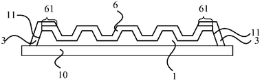
- FIG. 1 is a schematic view showing the structure of an array substrate according to an embodiment of the present invention.
- an array substrate includes: an array substrate 10, a structural layer 1, an organic light emitting diode layer 6 disposed on the top of the structural layer 1, and a passivation layer 3 covering the array substrate.
- the first encapsulant is filled between the array substrate and the color filter substrate, and the array substrate includes the array substrate 10, the structural layer 1, and the organic light emitting diode layer 6.
- Structural layer 1 is not A single layer, but a collection of layers that implement the functionality of the array substrate.
- the structural layer 1 may include: a gate electrode, a gate insulating layer, an active layer, an etch barrier layer, a source drain layer, a resin insulating layer, a pixel electrode layer (the pixel electrode layer may serve as an anode), and a pixel defining layer, as needed Multiple layers, but are not limited to this.
- the passivation layer 3 covers the edge of the organic light emitting diode layer 6, forming a non-light emitting region of the organic light emitting diode layer 6, while covering both sides of the structural layer 1.
- the organic light emitting diode layer is disposed at the passivation layer, that is, the edge of the organic light emitting diode layer is a non-light emitting region, and the rest (where the organic light emitting diode layer is not provided with a passivation layer) may be a light emitting region.
- the passivation layer 3 By covering the passivation layer 3 on the edge of the organic light emitting diode layer 6 (ie, the non-light emitting region) and the side of the structural layer 1, it is ensured that the full color is achieved by using the WOLED, and the upper electrode layer is overlapped by the spacer 4. At the same time as 18, the probability of moisture infiltrating from the side of the sealing structure is reduced. This ensures that the display panel composed of the array substrate has good water blocking performance and high panel reliability.
- the outer side of the array substrate 10 is provided with a chip-on-film area (COF) or a soft-plate-welded area (FPC) 8, which is disposed on the anisotropic conductive film (ACF) 9, and the anisotropic conductive film 9 is disposed on the array.
- COF chip-on-film area
- FPC soft-plate-welded area
- ACF anisotropic conductive film
- the passivation layer 3 is disposed between the light-emitting region 62 of the organic light-emitting diode layer 6 and the flip-chip film region or the soft-plate solder region 8.
- the passivation layer 3 is between the light-emitting region of the organic light-emitting diode layer 6 and the flip-chip film region or the soft-plate solder region 8, it can be ensured that the passivation layer 3 is in the first encapsulant and does not cover the organic light-emitting diode layer 6. Light emitting area.
- the passivation layer 3 may be a single layer structure or a multilayer stack structure.
- the passivation layer 3 may be one or a combination of silicon nitride, silicon oxide, aluminum oxide, and or titanium oxide.
- another embodiment of the present invention further provides an organic light emitting diode display panel comprising the array substrate of any of the above embodiments.
- an upper electrode layer 18 may be formed on the organic light emitting diode layer 6 of the array substrate, and the upper electrode layer 18 is a thin electrode layer disposed on the upper surface of the array organic light emitting diode layer 6.
- the organic light emitting diode display panel may further include a color filter substrate, wherein the color filter substrate includes the color film substrate 2.
- a color film layer 20 is formed on one side of the color filter substrate 2 facing the array substrate, an auxiliary electrode layer 5 is formed on the color film layer 20, and a spacer 4 is formed in the auxiliary electrode layer 5 (as shown in FIG. 3A).
- a spacer 4 is formed on the color filter layer 20 (as shown in FIG. 3B), and the auxiliary electrode layer 5 on the top of the spacer 4 contacts the upper electrode layer 18 of the array substrate as shown in FIG. 3A.
- FIG. 3A shows that the first encapsulant 15 can be filled between the color filter substrate 2 and the array substrate, and the passivation layer 3 is sealed by the first encapsulant 15.
- FIG. 3A illustrates an organic light emitting diode display panel according to another embodiment of the present invention, which may further include a second encapsulant 16 disposed on the periphery of the first encapsulant 15 for sealing the first encapsulant 15.
- the viscosity of the first sealant 15 may be less than the viscosity of the second sealant 16.
- sealant may be, for example, a first sealant or a first sealant and Second sealant.
- the second sealant is disposed outside the first sealant to further ensure the sealing performance of the display panel, and the surface uniformity of the first sealant can be improved. Moreover, since the first sealant directly contacts the organic light emitting diode layer 6, the organic light emitting diode layer 6 is damaged due to the tension of the contact surface during the curing process. By setting the viscosity of the first sealant to be smaller than the viscosity of the second sealant, it can be ensured that the contact surface of the first sealant and the organic light emitting diode layer 6 has only a small tension during the curing process, thereby reducing the organic light emitting diode layer. 6 damage. At the same time, the second sealant adopts a relatively large viscosity, which can ensure strong water repellency to the outside and improve the overall sealing performance.
- a metal trace 7 may be added to the structure of FIG. 3A.
- the organic light emitting diode display panel may further include a metal trace 7 disposed at the bottom of the spacer 4 and in contact with the auxiliary electrode layer 5. .
- the metal trace 7 may be made of a metal such as aluminum, molybdenum or silver or an alloy thereof.
- the conductivity of the auxiliary electrode layer 5 can be increased, and the resistance drop of the front surface of the OLED display panel can be lowered.
- the auxiliary electrode layer 5 is a transparent conductive film, and can be made of an oxide of a metal such as In, Sn, Zn, and Cd and a composite multi-oxide thin film material thereof, such as ITO (Indium Tin Oxide) or IZO (Indium Zinc Oxide). .
- the upper electrode layer may include at least one of the following: a silver layer, a magnesium-silver alloy layer, an indium tin oxide layer, an indium zinc oxide layer, and a composite layer on the metal layer covered with a transparent conductive film.
- Another embodiment of the present invention further provides a display device, which may include the organic light emitting diode display panel of any of the above embodiments.
- the display device of the embodiment of the present invention may be, for example, an electronic paper, a mobile phone, a watch, a tablet computer, a television, a display, a notebook computer, a digital photo frame, a navigator, or the like, and any product or component having a display function.
- the full color can be realized by using the WOLED, and the electrodes are overlapped by the spacer, and the display panel has good electrical conductivity and water blocking performance, and the high panel is trusted. degree.
- organic light emitting diode display panel of the embodiment of the present invention may further include other structures and components according to actual needs, and the organic light emitting diode display panel manufacturing method may further include other steps and details, but only Regardless of the improvement of the present invention, it will not be described herein.
Landscapes
- Electroluminescent Light Sources (AREA)
Abstract
L'invention concerne un substrat de réseau, un panneau d'affichage à diode électroluminescente organique et un appareil d'affichage. Le substrat de réseau comprend : un réseau de base (10), une couche de structure (1), une couche de diode électroluminescente organique (6) disposée sur la partie supérieure de la couche de structure (1) et une couche de passivation (3). La couche de passivation (3) recouvre une région non électroluminescente de la couche de diode électroluminescente organique (6) et une surface latérale de la couche de structure (1) dans le substrat de réseau. Le substrat de réseau peut permettre à un panneau d'affichage d'avoir de bonnes propriétés en termes de conductivité et de résistance à l'eau et de présente une fiabilité de panneau relativement élevée.
Applications Claiming Priority (2)
| Application Number | Priority Date | Filing Date | Title |
|---|---|---|---|
| CN201410363074.1A CN104112767B (zh) | 2014-07-28 | 2014-07-28 | 阵列基板、有机发光二极管显示面板和显示装置 |
| CN201410363074.1 | 2014-07-28 |
Publications (1)
| Publication Number | Publication Date |
|---|---|
| WO2016015421A1 true WO2016015421A1 (fr) | 2016-02-04 |
Family
ID=51709495
Family Applications (1)
| Application Number | Title | Priority Date | Filing Date |
|---|---|---|---|
| PCT/CN2014/092521 Ceased WO2016015421A1 (fr) | 2014-07-28 | 2014-11-28 | Substrat de réseau, panneau d'affichage à diode électroluminescente organique et appareil d'affichage |
Country Status (2)
| Country | Link |
|---|---|
| CN (1) | CN104112767B (fr) |
| WO (1) | WO2016015421A1 (fr) |
Cited By (3)
| Publication number | Priority date | Publication date | Assignee | Title |
|---|---|---|---|---|
| CN108074962A (zh) * | 2018-02-11 | 2018-05-25 | 京东方科技集团股份有限公司 | 阵列基板及其制作方法、显示面板、显示装置 |
| EP3688810A4 (fr) * | 2017-09-26 | 2021-07-07 | BOE Technology Group Co., Ltd. | Substrat d'affichage à diodes électroluminescentes organiques, appareil d'affichage à diodes électroluminescentes organiques, et procédé de fabrication de substrat d'affichage à diodes électroluminescentes organiques |
| US11127799B2 (en) | 2017-08-31 | 2021-09-21 | Boe Technology Group Co., Ltd. | Opposite substrate and preparation method thereof, display panel and packaging method |
Families Citing this family (10)
| Publication number | Priority date | Publication date | Assignee | Title |
|---|---|---|---|---|
| CN104112767B (zh) * | 2014-07-28 | 2017-09-19 | 京东方科技集团股份有限公司 | 阵列基板、有机发光二极管显示面板和显示装置 |
| CN104821329A (zh) * | 2015-05-04 | 2015-08-05 | 深圳市华星光电技术有限公司 | Oled显示装置 |
| CN106298839A (zh) * | 2015-06-03 | 2017-01-04 | 上海和辉光电有限公司 | 显示装置及其显示面板 |
| CN106228931A (zh) * | 2016-09-23 | 2016-12-14 | 深圳市国显科技有限公司 | 一种新型oled显示器及其制作工艺 |
| CN107293573A (zh) * | 2017-07-06 | 2017-10-24 | 京东方科技集团股份有限公司 | Oled基板和oled显示装置 |
| CN107316951B (zh) * | 2017-08-16 | 2019-01-29 | 京东方科技集团股份有限公司 | 封装基板及其制备方法、oled显示面板及其制备方法 |
| CN107565056B (zh) * | 2017-08-29 | 2019-11-01 | 京东方科技集团股份有限公司 | 一种封装基板、oled显示面板及其封装方法 |
| CN109791942B (zh) * | 2017-08-29 | 2024-01-26 | 京东方科技集团股份有限公司 | 有机发光二极管显示基板、有机发光二极管显示装置和制造有机发光二极管显示基板的方法 |
| CN109581725A (zh) * | 2018-12-18 | 2019-04-05 | 深圳市华星光电半导体显示技术有限公司 | 彩膜基板及显示面板 |
| CN110112311B (zh) * | 2019-05-10 | 2020-10-27 | 武汉华星光电半导体显示技术有限公司 | 一种显示面板及显示模组 |
Citations (6)
| Publication number | Priority date | Publication date | Assignee | Title |
|---|---|---|---|---|
| US4966862A (en) * | 1989-08-28 | 1990-10-30 | Cree Research, Inc. | Method of production of light emitting diodes |
| CN102263182A (zh) * | 2010-05-25 | 2011-11-30 | Lg伊诺特有限公司 | 发光器件及其制造方法、发光器件封装以及照明系统 |
| CN102347411A (zh) * | 2010-07-23 | 2012-02-08 | Lg伊诺特有限公司 | 发光器件、包括发光器件的发光器件封装以及照明系统 |
| CN102412355A (zh) * | 2010-09-17 | 2012-04-11 | Lg伊诺特有限公司 | 发光器件 |
| CN103545345A (zh) * | 2013-11-11 | 2014-01-29 | 京东方科技集团股份有限公司 | 一种显示面板及其制备方法、显示装置 |
| CN104112767A (zh) * | 2014-07-28 | 2014-10-22 | 京东方科技集团股份有限公司 | 阵列基板、有机发光二极管显示面板和显示装置 |
Family Cites Families (2)
| Publication number | Priority date | Publication date | Assignee | Title |
|---|---|---|---|---|
| CN103744238A (zh) * | 2013-12-10 | 2014-04-23 | 京东方科技集团股份有限公司 | 阵列基板及显示装置 |
| CN103715231B (zh) * | 2013-12-31 | 2016-11-23 | 京东方科技集团股份有限公司 | 有机发光显示面板、显示装置 |
-
2014
- 2014-07-28 CN CN201410363074.1A patent/CN104112767B/zh active Active
- 2014-11-28 WO PCT/CN2014/092521 patent/WO2016015421A1/fr not_active Ceased
Patent Citations (6)
| Publication number | Priority date | Publication date | Assignee | Title |
|---|---|---|---|---|
| US4966862A (en) * | 1989-08-28 | 1990-10-30 | Cree Research, Inc. | Method of production of light emitting diodes |
| CN102263182A (zh) * | 2010-05-25 | 2011-11-30 | Lg伊诺特有限公司 | 发光器件及其制造方法、发光器件封装以及照明系统 |
| CN102347411A (zh) * | 2010-07-23 | 2012-02-08 | Lg伊诺特有限公司 | 发光器件、包括发光器件的发光器件封装以及照明系统 |
| CN102412355A (zh) * | 2010-09-17 | 2012-04-11 | Lg伊诺特有限公司 | 发光器件 |
| CN103545345A (zh) * | 2013-11-11 | 2014-01-29 | 京东方科技集团股份有限公司 | 一种显示面板及其制备方法、显示装置 |
| CN104112767A (zh) * | 2014-07-28 | 2014-10-22 | 京东方科技集团股份有限公司 | 阵列基板、有机发光二极管显示面板和显示装置 |
Cited By (3)
| Publication number | Priority date | Publication date | Assignee | Title |
|---|---|---|---|---|
| US11127799B2 (en) | 2017-08-31 | 2021-09-21 | Boe Technology Group Co., Ltd. | Opposite substrate and preparation method thereof, display panel and packaging method |
| EP3688810A4 (fr) * | 2017-09-26 | 2021-07-07 | BOE Technology Group Co., Ltd. | Substrat d'affichage à diodes électroluminescentes organiques, appareil d'affichage à diodes électroluminescentes organiques, et procédé de fabrication de substrat d'affichage à diodes électroluminescentes organiques |
| CN108074962A (zh) * | 2018-02-11 | 2018-05-25 | 京东方科技集团股份有限公司 | 阵列基板及其制作方法、显示面板、显示装置 |
Also Published As
| Publication number | Publication date |
|---|---|
| CN104112767A (zh) | 2014-10-22 |
| CN104112767B (zh) | 2017-09-19 |
Similar Documents
| Publication | Publication Date | Title |
|---|---|---|
| WO2016015421A1 (fr) | Substrat de réseau, panneau d'affichage à diode électroluminescente organique et appareil d'affichage | |
| US9502683B2 (en) | Sealing portion structure for display device | |
| CN109148527B (zh) | 一种显示面板及显示装置 | |
| US9577215B2 (en) | Display device with glass frit sealing portion | |
| TWI715561B (zh) | 有機發光顯示設備 | |
| CN108630823B (zh) | 显示装置 | |
| US9541807B2 (en) | Flexible display device | |
| US9997589B2 (en) | Display device | |
| US10068954B2 (en) | Organic light-emitting display device | |
| KR20220020873A (ko) | 디스플레이 장치 | |
| CN109004005B (zh) | 显示面板及其制作方法、显示装置 | |
| CN107302016B (zh) | 一种有机发光二极管显示面板及其制作方法 | |
| KR102278334B1 (ko) | 유기 발광 표시 장치 | |
| CN107887526B (zh) | 显示面板及其制作方法、显示装置 | |
| KR20120076065A (ko) | 터치타입 유기전계 발광소자 | |
| US11737304B2 (en) | Display substrates, display panels and display devices | |
| KR20160017273A (ko) | 디스플레이 장치와, 이의 제조 방법 | |
| KR102877751B1 (ko) | 유기발광 표시장치 | |
| KR20240137520A (ko) | 유기 발광층을 포함하는 유기 발광 표시 장치 | |
| CN105655378A (zh) | 一种阵列基板和oled显示面板、制备方法及显示装置 | |
| JP2012209215A (ja) | 有機el装置の製造方法、電子機器 | |
| KR102758807B1 (ko) | 표시 장치 | |
| CN104393023B (zh) | 一种阵列基板及其制作方法、显示装置 | |
| CN110634887A (zh) | 阵列基板及其制作方法以及显示面板 | |
| US20240122041A1 (en) | Display device and method of manufacturing the same |
Legal Events
| Date | Code | Title | Description |
|---|---|---|---|
| 121 | Ep: the epo has been informed by wipo that ep was designated in this application |
Ref document number: 14898887 Country of ref document: EP Kind code of ref document: A1 |
|
| NENP | Non-entry into the national phase |
Ref country code: DE |
|
| 32PN | Ep: public notification in the ep bulletin as address of the adressee cannot be established |
Free format text: NOTING OF LOSS OF RIGHTS PURSUANT TO RULE 112(1) EPC (EPO FORM 1205A DATED 27/06/2017) |
|
| 122 | Ep: pct application non-entry in european phase |
Ref document number: 14898887 Country of ref document: EP Kind code of ref document: A1 |