WO2015129574A1 - Insulating substrate having through-hole - Google Patents
Insulating substrate having through-hole Download PDFInfo
- Publication number
- WO2015129574A1 WO2015129574A1 PCT/JP2015/054765 JP2015054765W WO2015129574A1 WO 2015129574 A1 WO2015129574 A1 WO 2015129574A1 JP 2015054765 W JP2015054765 W JP 2015054765W WO 2015129574 A1 WO2015129574 A1 WO 2015129574A1
- Authority
- WO
- WIPO (PCT)
- Prior art keywords
- hole
- insulating substrate
- alumina
- sintered body
- substrate
- Prior art date
- Legal status (The legal status is an assumption and is not a legal conclusion. Google has not performed a legal analysis and makes no representation as to the accuracy of the status listed.)
- Ceased
Links
Images


Classifications
-
- C—CHEMISTRY; METALLURGY
- C04—CEMENTS; CONCRETE; ARTIFICIAL STONE; CERAMICS; REFRACTORIES
- C04B—LIME, MAGNESIA; SLAG; CEMENTS; COMPOSITIONS THEREOF, e.g. MORTARS, CONCRETE OR LIKE BUILDING MATERIALS; ARTIFICIAL STONE; CERAMICS; REFRACTORIES; TREATMENT OF NATURAL STONE
- C04B35/00—Shaped ceramic products characterised by their composition; Ceramics compositions; Processing powders of inorganic compounds preparatory to the manufacturing of ceramic products
- C04B35/01—Shaped ceramic products characterised by their composition; Ceramics compositions; Processing powders of inorganic compounds preparatory to the manufacturing of ceramic products based on oxide ceramics
- C04B35/10—Shaped ceramic products characterised by their composition; Ceramics compositions; Processing powders of inorganic compounds preparatory to the manufacturing of ceramic products based on oxide ceramics based on aluminium oxide
- C04B35/111—Fine ceramics
-
- H—ELECTRICITY
- H05—ELECTRIC TECHNIQUES NOT OTHERWISE PROVIDED FOR
- H05K—PRINTED CIRCUITS; CASINGS OR CONSTRUCTIONAL DETAILS OF ELECTRIC APPARATUS; MANUFACTURE OF ASSEMBLAGES OF ELECTRICAL COMPONENTS
- H05K1/00—Printed circuits
- H05K1/02—Details
- H05K1/11—Printed elements for providing electric connections to or between printed circuits
- H05K1/115—Via connections; Lands around holes or via connections
-
- C—CHEMISTRY; METALLURGY
- C04—CEMENTS; CONCRETE; ARTIFICIAL STONE; CERAMICS; REFRACTORIES
- C04B—LIME, MAGNESIA; SLAG; CEMENTS; COMPOSITIONS THEREOF, e.g. MORTARS, CONCRETE OR LIKE BUILDING MATERIALS; ARTIFICIAL STONE; CERAMICS; REFRACTORIES; TREATMENT OF NATURAL STONE
- C04B35/00—Shaped ceramic products characterised by their composition; Ceramics compositions; Processing powders of inorganic compounds preparatory to the manufacturing of ceramic products
- C04B35/01—Shaped ceramic products characterised by their composition; Ceramics compositions; Processing powders of inorganic compounds preparatory to the manufacturing of ceramic products based on oxide ceramics
- C04B35/10—Shaped ceramic products characterised by their composition; Ceramics compositions; Processing powders of inorganic compounds preparatory to the manufacturing of ceramic products based on oxide ceramics based on aluminium oxide
- C04B35/111—Fine ceramics
- C04B35/117—Composites
- C04B35/119—Composites with zirconium oxide
-
- C—CHEMISTRY; METALLURGY
- C04—CEMENTS; CONCRETE; ARTIFICIAL STONE; CERAMICS; REFRACTORIES
- C04B—LIME, MAGNESIA; SLAG; CEMENTS; COMPOSITIONS THEREOF, e.g. MORTARS, CONCRETE OR LIKE BUILDING MATERIALS; ARTIFICIAL STONE; CERAMICS; REFRACTORIES; TREATMENT OF NATURAL STONE
- C04B35/00—Shaped ceramic products characterised by their composition; Ceramics compositions; Processing powders of inorganic compounds preparatory to the manufacturing of ceramic products
- C04B35/622—Forming processes; Processing powders of inorganic compounds preparatory to the manufacturing of ceramic products
- C04B35/626—Preparing or treating the powders individually or as batches ; preparing or treating macroscopic reinforcing agents for ceramic products, e.g. fibres; mechanical aspects section B
- C04B35/63—Preparing or treating the powders individually or as batches ; preparing or treating macroscopic reinforcing agents for ceramic products, e.g. fibres; mechanical aspects section B using additives specially adapted for forming the products, e.g.. binder binders
- C04B35/632—Organic additives
- C04B35/634—Polymers
-
- H—ELECTRICITY
- H01—ELECTRIC ELEMENTS
- H01B—CABLES; CONDUCTORS; INSULATORS; SELECTION OF MATERIALS FOR THEIR CONDUCTIVE, INSULATING OR DIELECTRIC PROPERTIES
- H01B17/00—Insulators or insulating bodies characterised by their form
- H01B17/56—Insulating bodies
-
- H—ELECTRICITY
- H01—ELECTRIC ELEMENTS
- H01B—CABLES; CONDUCTORS; INSULATORS; SELECTION OF MATERIALS FOR THEIR CONDUCTIVE, INSULATING OR DIELECTRIC PROPERTIES
- H01B3/00—Insulators or insulating bodies characterised by the insulating materials; Selection of materials for their insulating or dielectric properties
- H01B3/02—Insulators or insulating bodies characterised by the insulating materials; Selection of materials for their insulating or dielectric properties mainly consisting of inorganic substances
- H01B3/12—Insulators or insulating bodies characterised by the insulating materials; Selection of materials for their insulating or dielectric properties mainly consisting of inorganic substances ceramics
-
- H—ELECTRICITY
- H05—ELECTRIC TECHNIQUES NOT OTHERWISE PROVIDED FOR
- H05K—PRINTED CIRCUITS; CASINGS OR CONSTRUCTIONAL DETAILS OF ELECTRIC APPARATUS; MANUFACTURE OF ASSEMBLAGES OF ELECTRICAL COMPONENTS
- H05K1/00—Printed circuits
- H05K1/02—Details
- H05K1/03—Use of materials for the substrate
-
- H—ELECTRICITY
- H05—ELECTRIC TECHNIQUES NOT OTHERWISE PROVIDED FOR
- H05K—PRINTED CIRCUITS; CASINGS OR CONSTRUCTIONAL DETAILS OF ELECTRIC APPARATUS; MANUFACTURE OF ASSEMBLAGES OF ELECTRICAL COMPONENTS
- H05K1/00—Printed circuits
- H05K1/02—Details
- H05K1/03—Use of materials for the substrate
- H05K1/0306—Inorganic insulating substrates, e.g. ceramic, glass
-
- H—ELECTRICITY
- H05—ELECTRIC TECHNIQUES NOT OTHERWISE PROVIDED FOR
- H05K—PRINTED CIRCUITS; CASINGS OR CONSTRUCTIONAL DETAILS OF ELECTRIC APPARATUS; MANUFACTURE OF ASSEMBLAGES OF ELECTRICAL COMPONENTS
- H05K3/00—Apparatus or processes for manufacturing printed circuits
-
- H—ELECTRICITY
- H05—ELECTRIC TECHNIQUES NOT OTHERWISE PROVIDED FOR
- H05K—PRINTED CIRCUITS; CASINGS OR CONSTRUCTIONAL DETAILS OF ELECTRIC APPARATUS; MANUFACTURE OF ASSEMBLAGES OF ELECTRICAL COMPONENTS
- H05K3/00—Apparatus or processes for manufacturing printed circuits
- H05K3/0011—Working of insulating substrates or insulating layers
- H05K3/0017—Etching of the substrate by chemical or physical means
- H05K3/0026—Etching of the substrate by chemical or physical means by laser ablation
- H05K3/0029—Etching of the substrate by chemical or physical means by laser ablation of inorganic insulating material
-
- C—CHEMISTRY; METALLURGY
- C04—CEMENTS; CONCRETE; ARTIFICIAL STONE; CERAMICS; REFRACTORIES
- C04B—LIME, MAGNESIA; SLAG; CEMENTS; COMPOSITIONS THEREOF, e.g. MORTARS, CONCRETE OR LIKE BUILDING MATERIALS; ARTIFICIAL STONE; CERAMICS; REFRACTORIES; TREATMENT OF NATURAL STONE
- C04B2235/00—Aspects relating to ceramic starting mixtures or sintered ceramic products
- C04B2235/02—Composition of constituents of the starting material or of secondary phases of the final product
- C04B2235/30—Constituents and secondary phases not being of a fibrous nature
- C04B2235/32—Metal oxides, mixed metal oxides, or oxide-forming salts thereof, e.g. carbonates, nitrates, (oxy)hydroxides, chlorides
- C04B2235/3205—Alkaline earth oxides or oxide forming salts thereof, e.g. beryllium oxide
- C04B2235/3206—Magnesium oxides or oxide-forming salts thereof
-
- C—CHEMISTRY; METALLURGY
- C04—CEMENTS; CONCRETE; ARTIFICIAL STONE; CERAMICS; REFRACTORIES
- C04B—LIME, MAGNESIA; SLAG; CEMENTS; COMPOSITIONS THEREOF, e.g. MORTARS, CONCRETE OR LIKE BUILDING MATERIALS; ARTIFICIAL STONE; CERAMICS; REFRACTORIES; TREATMENT OF NATURAL STONE
- C04B2235/00—Aspects relating to ceramic starting mixtures or sintered ceramic products
- C04B2235/02—Composition of constituents of the starting material or of secondary phases of the final product
- C04B2235/30—Constituents and secondary phases not being of a fibrous nature
- C04B2235/32—Metal oxides, mixed metal oxides, or oxide-forming salts thereof, e.g. carbonates, nitrates, (oxy)hydroxides, chlorides
- C04B2235/3217—Aluminum oxide or oxide forming salts thereof, e.g. bauxite, alpha-alumina
-
- C—CHEMISTRY; METALLURGY
- C04—CEMENTS; CONCRETE; ARTIFICIAL STONE; CERAMICS; REFRACTORIES
- C04B—LIME, MAGNESIA; SLAG; CEMENTS; COMPOSITIONS THEREOF, e.g. MORTARS, CONCRETE OR LIKE BUILDING MATERIALS; ARTIFICIAL STONE; CERAMICS; REFRACTORIES; TREATMENT OF NATURAL STONE
- C04B2235/00—Aspects relating to ceramic starting mixtures or sintered ceramic products
- C04B2235/02—Composition of constituents of the starting material or of secondary phases of the final product
- C04B2235/30—Constituents and secondary phases not being of a fibrous nature
- C04B2235/32—Metal oxides, mixed metal oxides, or oxide-forming salts thereof, e.g. carbonates, nitrates, (oxy)hydroxides, chlorides
- C04B2235/3224—Rare earth oxide or oxide forming salts thereof, e.g. scandium oxide
- C04B2235/3225—Yttrium oxide or oxide-forming salts thereof
-
- C—CHEMISTRY; METALLURGY
- C04—CEMENTS; CONCRETE; ARTIFICIAL STONE; CERAMICS; REFRACTORIES
- C04B—LIME, MAGNESIA; SLAG; CEMENTS; COMPOSITIONS THEREOF, e.g. MORTARS, CONCRETE OR LIKE BUILDING MATERIALS; ARTIFICIAL STONE; CERAMICS; REFRACTORIES; TREATMENT OF NATURAL STONE
- C04B2235/00—Aspects relating to ceramic starting mixtures or sintered ceramic products
- C04B2235/02—Composition of constituents of the starting material or of secondary phases of the final product
- C04B2235/30—Constituents and secondary phases not being of a fibrous nature
- C04B2235/32—Metal oxides, mixed metal oxides, or oxide-forming salts thereof, e.g. carbonates, nitrates, (oxy)hydroxides, chlorides
- C04B2235/3231—Refractory metal oxides, their mixed metal oxides, or oxide-forming salts thereof
- C04B2235/3244—Zirconium oxides, zirconates, hafnium oxides, hafnates, or oxide-forming salts thereof
-
- C—CHEMISTRY; METALLURGY
- C04—CEMENTS; CONCRETE; ARTIFICIAL STONE; CERAMICS; REFRACTORIES
- C04B—LIME, MAGNESIA; SLAG; CEMENTS; COMPOSITIONS THEREOF, e.g. MORTARS, CONCRETE OR LIKE BUILDING MATERIALS; ARTIFICIAL STONE; CERAMICS; REFRACTORIES; TREATMENT OF NATURAL STONE
- C04B2235/00—Aspects relating to ceramic starting mixtures or sintered ceramic products
- C04B2235/02—Composition of constituents of the starting material or of secondary phases of the final product
- C04B2235/30—Constituents and secondary phases not being of a fibrous nature
- C04B2235/32—Metal oxides, mixed metal oxides, or oxide-forming salts thereof, e.g. carbonates, nitrates, (oxy)hydroxides, chlorides
- C04B2235/3281—Copper oxides, cuprates or oxide-forming salts thereof, e.g. CuO or Cu2O
-
- C—CHEMISTRY; METALLURGY
- C04—CEMENTS; CONCRETE; ARTIFICIAL STONE; CERAMICS; REFRACTORIES
- C04B—LIME, MAGNESIA; SLAG; CEMENTS; COMPOSITIONS THEREOF, e.g. MORTARS, CONCRETE OR LIKE BUILDING MATERIALS; ARTIFICIAL STONE; CERAMICS; REFRACTORIES; TREATMENT OF NATURAL STONE
- C04B2235/00—Aspects relating to ceramic starting mixtures or sintered ceramic products
- C04B2235/02—Composition of constituents of the starting material or of secondary phases of the final product
- C04B2235/30—Constituents and secondary phases not being of a fibrous nature
- C04B2235/34—Non-metal oxides, non-metal mixed oxides, or salts thereof that form the non-metal oxides upon heating, e.g. carbonates, nitrates, (oxy)hydroxides, chlorides
- C04B2235/3418—Silicon oxide, silicic acids or oxide forming salts thereof, e.g. silica sol, fused silica, silica fume, cristobalite, quartz or flint
-
- C—CHEMISTRY; METALLURGY
- C04—CEMENTS; CONCRETE; ARTIFICIAL STONE; CERAMICS; REFRACTORIES
- C04B—LIME, MAGNESIA; SLAG; CEMENTS; COMPOSITIONS THEREOF, e.g. MORTARS, CONCRETE OR LIKE BUILDING MATERIALS; ARTIFICIAL STONE; CERAMICS; REFRACTORIES; TREATMENT OF NATURAL STONE
- C04B2235/00—Aspects relating to ceramic starting mixtures or sintered ceramic products
- C04B2235/60—Aspects relating to the preparation, properties or mechanical treatment of green bodies or pre-forms
- C04B2235/602—Making the green bodies or pre-forms by moulding
- C04B2235/6023—Gel casting
-
- C—CHEMISTRY; METALLURGY
- C04—CEMENTS; CONCRETE; ARTIFICIAL STONE; CERAMICS; REFRACTORIES
- C04B—LIME, MAGNESIA; SLAG; CEMENTS; COMPOSITIONS THEREOF, e.g. MORTARS, CONCRETE OR LIKE BUILDING MATERIALS; ARTIFICIAL STONE; CERAMICS; REFRACTORIES; TREATMENT OF NATURAL STONE
- C04B2235/00—Aspects relating to ceramic starting mixtures or sintered ceramic products
- C04B2235/60—Aspects relating to the preparation, properties or mechanical treatment of green bodies or pre-forms
- C04B2235/606—Drying
-
- C—CHEMISTRY; METALLURGY
- C04—CEMENTS; CONCRETE; ARTIFICIAL STONE; CERAMICS; REFRACTORIES
- C04B—LIME, MAGNESIA; SLAG; CEMENTS; COMPOSITIONS THEREOF, e.g. MORTARS, CONCRETE OR LIKE BUILDING MATERIALS; ARTIFICIAL STONE; CERAMICS; REFRACTORIES; TREATMENT OF NATURAL STONE
- C04B2235/00—Aspects relating to ceramic starting mixtures or sintered ceramic products
- C04B2235/60—Aspects relating to the preparation, properties or mechanical treatment of green bodies or pre-forms
- C04B2235/612—Machining
-
- C—CHEMISTRY; METALLURGY
- C04—CEMENTS; CONCRETE; ARTIFICIAL STONE; CERAMICS; REFRACTORIES
- C04B—LIME, MAGNESIA; SLAG; CEMENTS; COMPOSITIONS THEREOF, e.g. MORTARS, CONCRETE OR LIKE BUILDING MATERIALS; ARTIFICIAL STONE; CERAMICS; REFRACTORIES; TREATMENT OF NATURAL STONE
- C04B2235/00—Aspects relating to ceramic starting mixtures or sintered ceramic products
- C04B2235/65—Aspects relating to heat treatments of ceramic bodies such as green ceramics or pre-sintered ceramics, e.g. burning, sintering or melting processes
- C04B2235/658—Atmosphere during thermal treatment
- C04B2235/6582—Hydrogen containing atmosphere
-
- C—CHEMISTRY; METALLURGY
- C04—CEMENTS; CONCRETE; ARTIFICIAL STONE; CERAMICS; REFRACTORIES
- C04B—LIME, MAGNESIA; SLAG; CEMENTS; COMPOSITIONS THEREOF, e.g. MORTARS, CONCRETE OR LIKE BUILDING MATERIALS; ARTIFICIAL STONE; CERAMICS; REFRACTORIES; TREATMENT OF NATURAL STONE
- C04B2235/00—Aspects relating to ceramic starting mixtures or sintered ceramic products
- C04B2235/65—Aspects relating to heat treatments of ceramic bodies such as green ceramics or pre-sintered ceramics, e.g. burning, sintering or melting processes
- C04B2235/66—Specific sintering techniques, e.g. centrifugal sintering
- C04B2235/661—Multi-step sintering
- C04B2235/662—Annealing after sintering
-
- C—CHEMISTRY; METALLURGY
- C04—CEMENTS; CONCRETE; ARTIFICIAL STONE; CERAMICS; REFRACTORIES
- C04B—LIME, MAGNESIA; SLAG; CEMENTS; COMPOSITIONS THEREOF, e.g. MORTARS, CONCRETE OR LIKE BUILDING MATERIALS; ARTIFICIAL STONE; CERAMICS; REFRACTORIES; TREATMENT OF NATURAL STONE
- C04B2235/00—Aspects relating to ceramic starting mixtures or sintered ceramic products
- C04B2235/70—Aspects relating to sintered or melt-casted ceramic products
- C04B2235/72—Products characterised by the absence or the low content of specific components, e.g. alkali metal free alumina ceramics
-
- C—CHEMISTRY; METALLURGY
- C04—CEMENTS; CONCRETE; ARTIFICIAL STONE; CERAMICS; REFRACTORIES
- C04B—LIME, MAGNESIA; SLAG; CEMENTS; COMPOSITIONS THEREOF, e.g. MORTARS, CONCRETE OR LIKE BUILDING MATERIALS; ARTIFICIAL STONE; CERAMICS; REFRACTORIES; TREATMENT OF NATURAL STONE
- C04B2235/00—Aspects relating to ceramic starting mixtures or sintered ceramic products
- C04B2235/70—Aspects relating to sintered or melt-casted ceramic products
- C04B2235/74—Physical characteristics
- C04B2235/77—Density
-
- C—CHEMISTRY; METALLURGY
- C04—CEMENTS; CONCRETE; ARTIFICIAL STONE; CERAMICS; REFRACTORIES
- C04B—LIME, MAGNESIA; SLAG; CEMENTS; COMPOSITIONS THEREOF, e.g. MORTARS, CONCRETE OR LIKE BUILDING MATERIALS; ARTIFICIAL STONE; CERAMICS; REFRACTORIES; TREATMENT OF NATURAL STONE
- C04B2235/00—Aspects relating to ceramic starting mixtures or sintered ceramic products
- C04B2235/70—Aspects relating to sintered or melt-casted ceramic products
- C04B2235/74—Physical characteristics
- C04B2235/78—Grain sizes and shapes, product microstructures, e.g. acicular grains, equiaxed grains, platelet-structures
- C04B2235/786—Micrometer sized grains, i.e. from 1 to 100 micron
-
- C—CHEMISTRY; METALLURGY
- C04—CEMENTS; CONCRETE; ARTIFICIAL STONE; CERAMICS; REFRACTORIES
- C04B—LIME, MAGNESIA; SLAG; CEMENTS; COMPOSITIONS THEREOF, e.g. MORTARS, CONCRETE OR LIKE BUILDING MATERIALS; ARTIFICIAL STONE; CERAMICS; REFRACTORIES; TREATMENT OF NATURAL STONE
- C04B2235/00—Aspects relating to ceramic starting mixtures or sintered ceramic products
- C04B2235/70—Aspects relating to sintered or melt-casted ceramic products
- C04B2235/95—Products characterised by their size, e.g. microceramics
-
- H—ELECTRICITY
- H05—ELECTRIC TECHNIQUES NOT OTHERWISE PROVIDED FOR
- H05K—PRINTED CIRCUITS; CASINGS OR CONSTRUCTIONAL DETAILS OF ELECTRIC APPARATUS; MANUFACTURE OF ASSEMBLAGES OF ELECTRICAL COMPONENTS
- H05K2201/00—Indexing scheme relating to printed circuits covered by H05K1/00
- H05K2201/09—Shape and layout
- H05K2201/09009—Substrate related
-
- H—ELECTRICITY
- H05—ELECTRIC TECHNIQUES NOT OTHERWISE PROVIDED FOR
- H05K—PRINTED CIRCUITS; CASINGS OR CONSTRUCTIONAL DETAILS OF ELECTRIC APPARATUS; MANUFACTURE OF ASSEMBLAGES OF ELECTRICAL COMPONENTS
- H05K3/00—Apparatus or processes for manufacturing printed circuits
- H05K3/0011—Working of insulating substrates or insulating layers
- H05K3/0014—Shaping of the substrate, e.g. by moulding
-
- Y—GENERAL TAGGING OF NEW TECHNOLOGICAL DEVELOPMENTS; GENERAL TAGGING OF CROSS-SECTIONAL TECHNOLOGIES SPANNING OVER SEVERAL SECTIONS OF THE IPC; TECHNICAL SUBJECTS COVERED BY FORMER USPC CROSS-REFERENCE ART COLLECTIONS [XRACs] AND DIGESTS
- Y10—TECHNICAL SUBJECTS COVERED BY FORMER USPC
- Y10T—TECHNICAL SUBJECTS COVERED BY FORMER US CLASSIFICATION
- Y10T428/00—Stock material or miscellaneous articles
- Y10T428/24—Structurally defined web or sheet [e.g., overall dimension, etc.]
- Y10T428/24273—Structurally defined web or sheet [e.g., overall dimension, etc.] including aperture
Definitions
- the present invention relates to a ceramic substrate having a large number of through holes for forming via conductors and through-hole conductors.
- a substrate for mounting an electronic device such as a SAW filter
- a substrate (via substrate) having a structure in which a through hole is provided in an insulating substrate such as ceramic and the hole is filled with a conductor to form a through electrode is used.
- insulating substrate such as ceramic
- the via substrate which is a component, is also required to be thin. It has been.
- the diameter of the through hole of such a substrate is required to be reduced to, for example, 100 ⁇ m or less, and it is required to form a large number at a high density.
- the material of the holding substrate is required to have a high resistance in order to suppress a leakage current between the wirings.
- the via substrate needs to be strong enough to withstand handling in the production process even when it is thinned.
- the via substrate is finally separated into pieces by dicing, good workability is required.
- the through electrode of the via substrate is manufactured by a thin film process such as vapor deposition or sputtering, the via substrate must be smooth on the front and back surfaces and inside of the through hole in order to avoid disconnection due to unevenness.
- the through hole is formed by a die press before firing, laser processing, laser processing after firing, or blasting (Patent Documents 1 to 3).
- alumina ceramics are widely used because they are excellent in mechanical strength, heat resistance, insulation and the like.
- alumina ceramics especially high-purity ones are excellent in translucency, alkali resistance, and plasma resistance, so they are widely used for arc tubes for high-intensity discharge lamps, members of semiconductor manufacturing equipment, dummy wafers, etc. (Patent Documents 4 to 7).
- alumina ceramic is used as a material for an insulating substrate having a through hole and a through electrode is produced by a thin film process such as vapor deposition or sputtering, if there are irregularities due to grain boundaries on the inner surface of the through hole, it is easy to break.
- the particle size of the alumina ceramic is increased, the number of grain boundaries is reduced, so that disconnection can be prevented, but the strength of the entire insulating substrate is lowered. For this reason, handling when the insulating substrate is thinned becomes difficult, and cracks and chipping are likely to occur during grinding, polishing, and dicing during the production of the insulating substrate.
- an insulating substrate is manufactured by mixing and sintering an alumina ceramic material and a glass material, and a through hole is formed by irradiating the base substrate with laser light. is doing. Thereby, a glass coating is formed on the inner wall surface facing the through hole of the insulating substrate, and the inner wall surface is smoothed.
- the thermal expansion coefficient of the coating facing the through hole is different from that of the alumina ceramic substrate, so the insulating substrate depends on the thermal cycle during the production process and after mounting. Is prone to breakage.
- the present invention is an insulating substrate in which through holes for conductors are arranged,
- the thickness of the insulating substrate is 25 to 100 ⁇ m
- the diameter of the through hole is 20 ⁇ m to 100 ⁇ m
- the insulating substrate includes a main body portion and an exposed region exposed to the through hole
- the insulating substrate is sintered with alumina.
- the alumina sintered body has a relative density of 99.5% or more
- the alumina sintered body has a purity of 99.9% or more
- the average particle size of the alumina sintered body in the main body portion is 3 to 6 ⁇ m.
- the average length of the plate-like alumina particles constituting the alumina sintered body in the exposed region is 8 to 25 ⁇ m.
- the present inventor has studied to form an insulating substrate having a through hole for forming a conductor with a high-purity alumina sintered body. At this time, it is necessary to keep the strength high even if the insulating substrate is thinned by miniaturizing the alumina particles of the alumina sintered body. However, if a through hole is formed in such an insulating substrate, disconnection is likely to occur when a conductive film is formed on the inner wall surface of the through hole.
- the glass component was mixed with the ceramics constituting the insulating substrate, so that the glass component was precipitated on the inner wall surface facing the through hole. This should prevent disconnection of the conductor formed on the inner wall surface of the through hole.
- the present inventors refined the particles of the alumina sintered body constituting the insulating substrate and at the same time made it as highly pure as possible to prevent the precipitation of the glass component on the inner wall surface facing the through hole. Along with this, an exposed region made of plate-like particles was formed along the inner wall surface facing the through hole. As a result, it has been found that chipping and cracking can be prevented during processing such as grinding, polishing and dicing, and that chipping and cracking can be prevented even when a thermal cycle is applied, and the present invention has been achieved.
- (A) is a top view which shows typically the insulated substrate 1 in which the through-hole 2 was formed
- (b) is a schematic diagram which shows the shape abnormality of the through-hole 2
- (c) is a through-hole. It is sectional drawing which shows typically the insulating substrate 1 in which 2 was formed.
- (A) is an enlarged view which shows the through-hole of the insulated substrate 1, and its periphery
- (b) is a schematic diagram of a through-hole, an exposure area
- FIG. 2 It is a microscope picture corresponding to the schematic diagram of FIG. It is a flowchart which shows an example of the suitable manufacturing procedure of an insulated substrate. It is a flowchart which shows an example of the suitable manufacturing procedure of an insulated substrate. The temperature profile applied by the heat cycle test is shown. 2 is an enlarged photograph of a through hole of an insulating substrate 1 and its surroundings.
- the insulating substrate 1 is provided with one main surface 1a and the other main surface 1b, and a through-hole penetrating between the main surfaces 1a and 1b. 2 is formed in large numbers.
- the insulating substrate 1 includes a main body portion 5 and an exposed region 4 provided in a portion exposed to the through hole 2 of the main body portion 5.
- the exposed region 4 faces the through hole 2, and the surface of the exposed region 4 constitutes the inner wall surface 3.
- the main body portion 5 and the exposed region 4 are made of an alumina sintered body, and their ceramic structures are integrated.
- a predetermined conductor can be formed in the through hole.
- a conductor Ag, Au, Cu, Pd, or a mixture thereof, or a paste obtained by mixing a small amount of glass component with these, is filled into the hole inner surface, and then baked at 400 to 900 ° C. to be fixed.
- Examples of the conductors (via conductors), conductors printed only on the inner surfaces of the holes, and baked in the same manner (through-hole conductors) can be exemplified, but the form of the conductors is not particularly limited.
- predetermined wirings, pads, and the like are formed on the main surfaces 1a and 1b of the substrate.
- the insulating substrate is an integral relay substrate.
- the thickness T (see FIG. 2) of the insulating substrate is 25 to 100 ⁇ m. From the viewpoint of the strength required for handling the insulating substrate, the thickness of the insulating substrate is 25 ⁇ m or more, and more preferably 50 ⁇ m or more.
- the diameter W of the through hole formed in the insulating substrate is 20 ⁇ m or more. This through hole diameter is more preferably 25 ⁇ m or more from the viewpoint of ease of molding. Further, in order to increase the density of the through holes, the through hole diameter W is set to 100 ⁇ m or less, more preferably 80 ⁇ m or less.
- the distance D (distance between the nearest through holes) between adjacent through holes 2 is preferably 50 ⁇ m or more, and more preferably 100 ⁇ m or more, from the viewpoint of suppressing breakage and cracks. Further, the distance D between adjacent through holes 2 is preferably 1000 ⁇ m or less, and more preferably 500 ⁇ m or less, from the viewpoint of improving the density of the through holes.
- the relative density of the alumina sintered body constituting the insulating substrate is set to 99.5% or more, more preferably 99.6% or more. This upper limit is not particularly limited and may be 100%.
- the porosity is determined as follows. That is, the cross section (cross section perpendicular to the bonding surface) of the handle substrate is mirror-polished and thermally etched to highlight the crystal grain boundary, and then an optical micrograph (200 times) is taken. Then, a layered visual field of 0.1 mm is set in the thickness direction (direction perpendicular to the bonding surface) of the handle substrate and 1.0 mm in the direction horizontal to the bonding surface. Then, for each visual field, the total area of pores having a size of 0.5 ⁇ m or more is calculated, and the visual field area ratio is calculated from the obtained pore area to obtain the porosity.
- the average particle size of the alumina sintered body particles 5a constituting the main body portion 5 (see FIG. 2) of the insulating substrate is 3 to 6 ⁇ m.
- the average particle size of the alumina sintered body is 5 ⁇ m or less.
- the thickness is more preferably 3.5 ⁇ m or more.
- the average length of the alumina sintered body particles 4 constituting the region 4 exposed to the through hole of the insulating substrate is 8 to 25 ⁇ m.
- the average length of the sintered body constituting the region 4 (see FIG. 2) exposed to the through hole of the insulating substrate is 10 ⁇ m or more.
- the average length of the sintered body constituting the exposed region 4 is 25 ⁇ m or less, it is possible to prevent cracks during thermal cycle application. From this viewpoint, it is more preferable that the average length of the sintered body constituting the region 4 exposed to the through hole of the insulating substrate is 15 ⁇ m or less.
- FIG. 4 is a schematic diagram for explaining a method for calculating the average length of the particles, and corresponds to FIG. However, in FIG. 4, the insulating substrate is turned sideways.
- FIG. 5 is a photograph corresponding to FIG.
- the insulating substrate is cleaved at the through-hole portion, a micrograph (200 times) of the inner surface of the hole is taken from the cut section, and the length of the particle crossed by the unit-length straight line S is measured. This is carried out at three different places, and the average length of the particles crossed by the three straight lines is defined as the average length.
- the average length of the particles 1 to 10 is defined as the average length.
- the straight line S is drawn so as to penetrate from the front surface to the back surface of the insulating substrate in parallel with the central axis C of the through hole (FIG. 2A).
- the “unit length” is equal to the thickness T of the substrate.
- the thickness A of the plate-like particles in the exposed region 4 of the insulating substrate may be at least one crystal 4a, specifically at least 0.5 ⁇ m or more, preferably 1 to 3 ⁇ m. Further, the aspect ratio of the plate-like particle 4 is preferably 2.5 or more, and more preferably 10 or more. However, the aspect ratio of the plate-like particle 4 is the average length / thickness A.
- the alumina purity of the alumina sintered body constituting the insulating substrate is 99.9% or more. Thereby, precipitation of the glass component in the exposed region facing the through hole can be prevented.
- the alumina purity of the alumina sintered body is determined by dissolving a sample pulverized in a powder form by sulfuric acid decomposition with sulfuric acid, and analyzing the solution by ICP emission spectrometry.
- 200 to 800 ppm by mass of zirconia, 150 to 300 ppm by mass of magnesia and 10 to 30 ppm by mass of yttria are added as sintering aids to the alumina sintered body constituting the insulating substrate.
- the breakdown voltage of sapphire is 47 kV / mm, and the breakdown voltage of a normal alumina sintered body is 12 kV / mm. Furthermore, the dielectric loss tangent of this alumina sintered body is equivalent to that of sapphire, which is much lower than the dielectric loss tangent of a normal alumina sintered body, for example, about 1/10.
- the addition amount of zirconia in the alumina sintered body constituting the insulating substrate is more preferably 300 mass ppm or more, and further preferably 600 mass ppm or less.
- the amount of magnesia added to the alumina sintered body constituting the insulating substrate is more preferably 200 ppm by mass or more, and further preferably 280 ppm by mass or less.
- the amount of yttria added to the alumina sintered body constituting the insulating substrate is more preferably 12 mass ppm or more, and further preferably 20 mass ppm or less.
- abnormal shape of the through holes may occur. For example, as shown in FIG. 1B, such a through hole 2 may bulge toward one side to form a bulged portion 3.
- voids due to coarse pores remaining in the dense alumina sintered body are connected to the relatively fine through-hole 2 and integrated. It was considered a thing. Such voids are caused by coarse pores having a diameter of 10 ⁇ m or more.
- the inventor further examined the material of the dense alumina sintered body based on such knowledge. Since a large number of through electrodes are formed on this substrate, it is desirable to employ a high-purity alumina sintered body in order to achieve high resistance. At the same time, however, coarse pores having a diameter of 10 ⁇ m or more are controlled by controlling the average particle diameter of the sintered body constituting the main body portion of the insulating substrate to 3 to 6 ⁇ m and the relative density to 99.5% or more. Can be suppressed, and abnormal shape of the through hole can be prevented.
- the method for forming the through hole in the insulating substrate is not particularly limited.
- a through hole can be formed in a green sheet of an insulating substrate by pins or laser processing.
- a through-hole can also be formed in a blank board
- FIGS. 6 and 7 are flow charts illustrating procedures suitable for manufacturing the insulating substrate of the present invention.
- a slurry for an alumina molded body is prepared.
- the sintering aid powder as described above is added to high-purity alumina powder having a purity of 99.9% or more (more preferably 99.95% or more).
- high-purity alumina powder examples include high-purity alumina powder manufactured by Daimei Chemical Co., Ltd.
- the method for forming the polycrystalline ceramic sintered body is not particularly limited, and may be any method such as a doctor blade method, an extrusion method, or a gel cast method.
- the substrate is manufactured using the following doctor blade method.
- a slurry is prepared by dispersing polyvinyl butyral resin (PVB resin) or acrylic resin as a binder together with ceramic powder in a dispersion medium together with a plasticizer and a dispersant. After forming into a tape shape, the dispersion medium is dried to solidify the slurry.
- PVB resin polyvinyl butyral resin
- acrylic resin acrylic resin
- a large number of through holes are formed in the molded body by punch pressing or laser processing at the stage of the molded body, and a paste in which alumina particles are dispersed in an organic solvent is applied to the inner surface of the hole. Keep it. At this time, the ceramic component contained in the paste is only alumina particles, and the aforementioned sintering aid is not added. Thereby, the density
- the paste can be applied by through-hole printing by screen printing, dipping, spraying, or the like. In the example of FIG. 7, it is not necessary to form a through hole in the molded body.
- the molded body is preferably calcined in the air, and then calcined in hydrogen.
- the sintering temperature during the main firing is preferably 1500 to 1900 ° C., more preferably 1550 to 1750 ° C., from the viewpoint of densification of the sintered body.
- the firing is performed in such a manner that a substrate is placed on a flat plate made of a refractory metal such as molybdenum, a plate of molybdenum is placed thereon, and the substrate is sandwiched from above and below.
- a refractory metal such as molybdenum
- a plate of molybdenum is placed thereon, and the substrate is sandwiched from above and below.
- an additional annealing treatment can be performed to correct the warp.
- This annealing temperature is preferably within the maximum temperature ⁇ 100 ° C. during firing from the viewpoint of promoting the discharge of the sintering aid while preventing deformation and abnormal grain growth, and the maximum temperature is 1900 ° C. or less. More preferably it is.
- the annealing time is preferably 1 to 6 hours.
- a plate made of molybdenum or the like with a hole is placed on the corresponding part of the through hole of the substrate to facilitate the flow of hydrogen gas through the through hole, thereby promoting grain growth in the exposed region of the through hole. be able to.
- the blank substrate thus obtained is roughly polished.
- precision polishing can be performed for the purpose of reducing the Ra of the main surface.
- CMP Chemical Mechanical Polishing
- As the polishing slurry used for this a slurry in which abrasive grains having a particle size of 30 nm to 200 nm are dispersed in an alkali or neutral solution is used.
- the abrasive material include silica, alumina, diamond, zirconia, and ceria, which are used alone or in combination.
- a hard urethane pad, a nonwoven fabric pad, and a suede pad can be illustrated as a polishing pad.
- the annealing process can be performed after the rough polishing process before the final precision polishing process is performed.
- the atmospheric gas for the annealing treatment include air, hydrogen, nitrogen, argon, and vacuum.
- the annealing temperature is preferably 1200 to 1600 ° C., and the annealing time is preferably 2 to 12 hours.
- the through hole is not formed in the molded body, and the sintered blank substrate is roughly polished, and then the through hole is formed in the blank substrate by laser processing.
- Laser processing is preferably performed as follows.
- a through-hole is formed by irradiating the substrate surface with a short pulse laser.
- the pulse width is generally less than milliseconds (1 / 1e-3 seconds).
- gas (CO2) or solid (YAG) is used as the laser source.
- CO2 gas
- YAG solid
- the hole diameter and hole shape can be adjusted by the mask diameter, laser output, pulse width, and number of shots. Of these, it is common to adjust the hole diameter according to the mask diameter, laser output, and pulse width, and to set the minimum required number for penetrating the substrate as the number of shots.
- the particle size of the exposed area can be controlled.
- Example 1 The insulating substrate of the present invention was manufactured according to the procedure described with reference to FIG. Specifically, a slurry in which the following components were mixed was prepared.
- (Raw material powder) ⁇ -alumina powder having a specific surface area of 3.5 to 4.5 m 2 / g and an average primary particle size of 0.35 to 0.45 ⁇ m (alumina purity 99.99%) 100 parts by mass • MgO (magnesia) 250 ppm ⁇ ZrO 2 (zirconia) 400ppm ⁇ Y 2 O 3 (yttria) 15ppm (Dispersion medium) ⁇ 45 parts by weight of 2-ethylhexanol (binder) ⁇ PVB resin 4 parts by weight (dispersant) ⁇ Polymer surfactant 3 parts by weight (plasticizer) ⁇ DOP 0.1 parts by weight
- this slurry was formed into a tape shape so as to be 0.25 mm in terms of the thickness after firing, and converted into a size after firing so that it becomes ⁇ 100 mm.
- the obtained powder compact is calcined at 1240 ° C. in the atmosphere (preliminary firing), and then the substrate is placed on a molybdenum plate and heated at a rate of 1300 ° C. to 1550 ° C. in an atmosphere of hydrogen 3: nitrogen 1. Was kept at 1550 ° C. for 2.5 hours and baked to obtain a blank substrate.
- the blank substrate was laser processed under the following conditions to form through holes having the following dimensions.
- CO 2 laser wavelength 10.6 ⁇ m
- Pulse 1000Hz- On time 5 ⁇ s
- Laser mask diameter 0.9 mm
- Number of shots 40 times Through-hole system
- W 0.05 mm
- Through hole spacing D 0.12 mm
- an annealing treatment was performed at 1300 ° C. in the atmosphere for 5 hours, and grinding with a grinder, lapping with diamond abrasive grains, and polishing with CMP liquid were sequentially performed.
- the thickness of the plate-like particles on the inner wall of the through-hole was found to differ depending on the location, It was in the range of 5-5 ⁇ m. Further, the aspect ratio of the plate-like particles on the inner wall of the through hole was 2.5 to 20.
- a metal film by vapor deposition was formed on the front and back surfaces of the obtained substrate and the inner surface of the through hole, and then separated into pieces of 2 mm by dicing.
- Examples 2 to 5 The experiment was performed in the same manner as in Example 1. However, the baking temperature, the laser processing conditions, the annealing conditions, and the laser processing conditions for the through holes were adjusted to prepare substrates having various particle sizes shown in Table 1, and the same evaluation as in Example 1 was performed. The obtained evaluation results are shown in Table 1.
- the thickness of the plate-like particles on the inner wall of the through hole was in the range of 0.5 to 5 ⁇ m. Further, the aspect ratio of the plate-like particles on the inner wall of the through hole was 2.5 to 20.
- Example 1 It was created by the same method as in Example 1. However, an alumina raw material with a purity of 96% was used as the alumina raw material powder. The obtained substrate was evaluated in the same manner as in Example 1, and the evaluation results are shown in Table 2.
- Comparative Example 1 a glass component was deposited in an exposed region facing the through hole of the insulating substrate. As a result, disconnection failure was prevented, but there were many cracks and chipping after dicing and cracks and chipping after the thermal shock test.
- the average length of the plate-like particles in the exposed region is as small as 6 ⁇ m, but there are many disconnection defects and cracks after dicing.
- the average length of the plate-like particles in the exposed region is 30 ⁇ m and the average particle size in the main body portion is 8 ⁇ m, but there are many cracks after dicing and cracks after thermal cycling.
- the average particle size in the main body portion is 15 ⁇ m, but there are many cracks and chipping after dicing and cracks and chipping after the thermal shock test.
- the average length in the exposed region is 30 ⁇ m, but there are many cracks after the thermal shock test.
- Comparative Example 6 the average length of the plate-like particles in the exposed region is 35 ⁇ m and the average particle size in the main body portion is 2 ⁇ m, but there are many cracks after dicing.
- Comparative Example 7 the alumina purity is 98% and the average particle size in the main body is 1 ⁇ m, but there are many cracks after dicing.
- the average length of the plate-like particles in the exposed region is 15 ⁇ m and the average particle size in the main body portion is 8 ⁇ m, but there are many cracks after dicing and cracks after thermal cycling.
- the average length of the plate-like particles in the exposed region is 15 ⁇ m and the average particle size in the main body portion is 1 ⁇ m, but there are many cracks after dicing.
- the average length of the plate-like particles in the exposed region is 6 ⁇ m and the average particle size in the main body portion is 5 ⁇ m, but there are many disconnections.
Landscapes
- Engineering & Computer Science (AREA)
- Chemical & Material Sciences (AREA)
- Ceramic Engineering (AREA)
- Manufacturing & Machinery (AREA)
- Microelectronics & Electronic Packaging (AREA)
- Inorganic Chemistry (AREA)
- Organic Chemistry (AREA)
- Structural Engineering (AREA)
- Materials Engineering (AREA)
- Composite Materials (AREA)
- Physics & Mathematics (AREA)
- Optics & Photonics (AREA)
- Compositions Of Oxide Ceramics (AREA)
Abstract
Description
本発明は、ビア導体やスルーホール導体を形成するための貫通孔を多数有するセラミック基板に関するものである。 The present invention relates to a ceramic substrate having a large number of through holes for forming via conductors and through-hole conductors.
SAWフィルター等の電子デバイスを実装するための基板として、セラミック等の絶縁基板に貫通穴を設け、その穴を導体で埋め、貫通電極とする構造の基板(ビア基板)が用いられている。近年は携帯電話に代表される通信機器の小型化に伴い、使用される電子デバイスにも小型化、低背化が求められており、その構成要素であるビア基板についても同様に薄板化が求められている。 As a substrate for mounting an electronic device such as a SAW filter, a substrate (via substrate) having a structure in which a through hole is provided in an insulating substrate such as ceramic and the hole is filled with a conductor to form a through electrode is used. In recent years, along with miniaturization of communication equipment typified by mobile phones, electronic devices used are also required to be miniaturized and low profiled, and the via substrate, which is a component, is also required to be thin. It has been.
更に、こうした基板の貫通孔の直径は、例えば100μm以下とする細径化が求められており、また高密度で多数形成することが求められている。また、保持基板の材質には、配線間のリーク電流を押さえるために高い抵抗が求められる。 Furthermore, the diameter of the through hole of such a substrate is required to be reduced to, for example, 100 μm or less, and it is required to form a large number at a high density. Further, the material of the holding substrate is required to have a high resistance in order to suppress a leakage current between the wirings.
このため、ビア基板には、薄板化した際も、生産プロセスにおけるハンドリングに耐えうるだけの強度が必要とされる。一方で、最終的にはダイシングによりビア基板を個片化することから、加工性が良好であることが必要である。 For this reason, the via substrate needs to be strong enough to withstand handling in the production process even when it is thinned. On the other hand, since the via substrate is finally separated into pieces by dicing, good workability is required.
ビア基板の貫通電極は、蒸着、スパッタ等の薄膜プロセスにより作製されるため、凹凸による断線等を避けるためビア基板の表裏面、貫通孔内部が平滑であることが求められる。貫通孔は、焼成前の金型プレス、レーザー加工、焼成後のレーザー加工、ブラスト加工により形成される(特許文献1~3)。
Since the through electrode of the via substrate is manufactured by a thin film process such as vapor deposition or sputtering, the via substrate must be smooth on the front and back surfaces and inside of the through hole in order to avoid disconnection due to unevenness. The through hole is formed by a die press before firing, laser processing, laser processing after firing, or blasting (
ビア基板の材料としては、アルミナセラミックスが機械的強度、耐熱性、絶縁性等に優れることから、広く使用されている。また、アルミナセラミックスの中でも、特に高純度のものは透光性、耐アルカリ性、耐プラズマ性にも優れることから、高輝度放電灯用の発光管や半導体製造装置の部材、ダミーウエハー等に広く使用されている(特許文献4~7)。
As a material for via substrates, alumina ceramics are widely used because they are excellent in mechanical strength, heat resistance, insulation and the like. Among alumina ceramics, especially high-purity ones are excellent in translucency, alkali resistance, and plasma resistance, so they are widely used for arc tubes for high-intensity discharge lamps, members of semiconductor manufacturing equipment, dummy wafers, etc. (
アルミナセラミックスを、貫通孔を有する絶縁基板の材質として用い、蒸着、スパッタといった薄膜プロセスで貫通電極を作製する場合、貫通孔内面に粒界による凹凸があると、それが原因となり断線しやすくなる。一方、アルミナセラミックスの粒径を大きくすると、粒界の数が減るため断線は防止できるが、絶縁基板全体の強度が低下する。このため、絶縁基板を薄板化した際のハンドリングが難しくなり、また、絶縁基板作製時の研削、研磨工程やダイシングの際、クラックやチッピングが起こりやすくなる。 When alumina ceramic is used as a material for an insulating substrate having a through hole and a through electrode is produced by a thin film process such as vapor deposition or sputtering, if there are irregularities due to grain boundaries on the inner surface of the through hole, it is easy to break. On the other hand, when the particle size of the alumina ceramic is increased, the number of grain boundaries is reduced, so that disconnection can be prevented, but the strength of the entire insulating substrate is lowered. For this reason, handling when the insulating substrate is thinned becomes difficult, and cracks and chipping are likely to occur during grinding, polishing, and dicing during the production of the insulating substrate.
特許文献2記載の絶縁基板においては、例えばアルミナセラミックス材料とガラス材料とを混合して焼結させることで絶縁基板を製造しており、このベース基板にレーザ光を照射することで貫通孔を形成している。これによって、絶縁基板の貫通孔に面する内壁面にガラスコーティングを形成し、内壁面を平滑にする。しかし、実際にこうした絶縁基板を作製してみると、貫通孔に面するコーティングの熱膨張係数が、基材であるアルミナセラミックスと異なることから、生産プロセス中および実装後の熱サイクルによって、絶縁基板が破損しやすくなる。
In the insulating substrate described in
本発明の課題は、導電部形成用の貫通孔を有する絶縁基板において、研削、研磨やダイシング等の加工の際にチッピングやクラックを防止でき、かつ熱サイクルを加えたときにチッピングやクラックを防止できるようにすることである。 It is an object of the present invention to prevent chipping and cracks during processing such as grinding, polishing and dicing in an insulating substrate having through holes for forming conductive portions, and to prevent chipping and cracks when a thermal cycle is applied. Is to be able to do it.
本発明は、導体用の貫通孔が配列されている絶縁基板であって、
絶縁基板の厚さが25~100μmであり、貫通孔の径が20μm~100μmであり、絶縁基板が、本体部分と、貫通孔に露出する露出領域とを備えており、絶縁基板がアルミナ焼結体からなり、アルミナ焼結体の相対密度が99.5%以上であり、アルミナ焼結体の純度が99.9%以上であり、本体部分におけるアルミナ焼結体の平均粒径が3~6μmであり、露出領域におけるアルミナ焼結体を構成する板状のアルミナ粒子の平均長さが8~25μmであることを特徴とする。
The present invention is an insulating substrate in which through holes for conductors are arranged,
The thickness of the insulating substrate is 25 to 100 μm, the diameter of the through hole is 20 μm to 100 μm, the insulating substrate includes a main body portion and an exposed region exposed to the through hole, and the insulating substrate is sintered with alumina. The alumina sintered body has a relative density of 99.5% or more, the alumina sintered body has a purity of 99.9% or more, and the average particle size of the alumina sintered body in the main body portion is 3 to 6 μm. The average length of the plate-like alumina particles constituting the alumina sintered body in the exposed region is 8 to 25 μm.
本発明者は、導体形成用の貫通孔を有する絶縁基板を、高純度のアルミナ焼結体によって形成することを検討した。この際、アルミナ焼結体のアルミナ粒子を微細化することで、絶縁基板を薄くしてもその強度を高く維持する必要がある。しかし、こうした絶縁基板に貫通孔を形成すると、貫通孔内壁面に導電膜を形成したときに断線が生じやすくなる。 The present inventor has studied to form an insulating substrate having a through hole for forming a conductor with a high-purity alumina sintered body. At this time, it is necessary to keep the strength high even if the insulating substrate is thinned by miniaturizing the alumina particles of the alumina sintered body. However, if a through hole is formed in such an insulating substrate, disconnection is likely to occur when a conductive film is formed on the inner wall surface of the through hole.
このため、特許文献2記載のように、絶縁基板を構成するセラミックス中にガラス成分を混合することで、貫通孔に面する内壁面にガラス成分を析出させることも検討した。これによって、貫通孔内壁面に形成する導体の断線を防止できるはずである。しかし、この場合には、絶縁基板に熱サイクルが加わると、クラックやチッピングが発生しやすくなることがわかった。
For this reason, as described in
このため、本発明者は、絶縁基板を構成するアルミナ焼結体の粒子を微細化するのと同時に、できるだけ高純度化し、貫通孔に面する内壁面へのガラス成分の析出を防止した。これと共に、貫通孔に面する内壁面に沿って、板状粒子からなる露出領域を形成した。この結果、研削、研磨やダイシング等の加工の際にチッピングやクラックを防止でき、かつ熱サイクルを加えたときにもチッピングやクラックを防止できることを見いだし、本発明に到達した。 For this reason, the present inventors refined the particles of the alumina sintered body constituting the insulating substrate and at the same time made it as highly pure as possible to prevent the precipitation of the glass component on the inner wall surface facing the through hole. Along with this, an exposed region made of plate-like particles was formed along the inner wall surface facing the through hole. As a result, it has been found that chipping and cracking can be prevented during processing such as grinding, polishing and dicing, and that chipping and cracking can be prevented even when a thermal cycle is applied, and the present invention has been achieved.
以下、適宜図面を参照しつつ、本発明を更に詳細に説明する。
図1(a)、(c)に示すように、絶縁基板1には一方の主面1aと他方の主面1bとが設けられており、主面1aと1bとの間を貫通する貫通孔2が多数形成されている。
Hereinafter, the present invention will be described in more detail with reference to the drawings as appropriate.
As shown in FIGS. 1A and 1C, the
図2に示すように、絶縁基板1は、本体部分5と、本体部分5の貫通孔2に露出する部分に設けられた露出領域4とを備えている。露出領域4は、貫通孔2に面しており、露出領域4の表面が内壁面3を構成している。本体部分5と露出領域4とはアルミナ焼結体からなっており、両者のセラミックス組織は一体化している。
As shown in FIG. 2, the
貫通孔内には所定の導体を形成可能である。こうした導体としては、Ag、Au、Cu、Pd、またはその混合物や、これらに少量のガラス成分を混合してペースト化したものを孔内面に充填した後、400~900℃で焼付けして固定化させたものや(ビア導体)、孔の内面にのみ導体を印刷し、同様に焼付けしたもの(スルホール導体)などを例示できるが、導体の形態は特に限定されるものではない。また、基板の主面1a、1bには、所定の配線やパッドなどを形成する。また,絶縁基板は、一体の中継基板とする。
A predetermined conductor can be formed in the through hole. As such a conductor, Ag, Au, Cu, Pd, or a mixture thereof, or a paste obtained by mixing a small amount of glass component with these, is filled into the hole inner surface, and then baked at 400 to 900 ° C. to be fixed. Examples of the conductors (via conductors), conductors printed only on the inner surfaces of the holes, and baked in the same manner (through-hole conductors) can be exemplified, but the form of the conductors is not particularly limited. Further, predetermined wirings, pads, and the like are formed on the
本発明の絶縁基板には、導体用の貫通孔が配列されている。ここで、絶縁基板の厚さT(図2参照)は25~100μmである。絶縁基板のハンドリングに必要な強度の観点からは、絶縁基板の厚さを25μm以上とするが、50μm以上が更に好ましい。 In the insulating substrate of the present invention, through holes for conductors are arranged. Here, the thickness T (see FIG. 2) of the insulating substrate is 25 to 100 μm. From the viewpoint of the strength required for handling the insulating substrate, the thickness of the insulating substrate is 25 μm or more, and more preferably 50 μm or more.
絶縁基板に形成する貫通孔の径W(図1、図2参照)は20μm以上である。この貫通孔径は、成形しやすさの観点からは、25μm以上が更に好ましい。また、貫通孔の密度を上げるためには、貫通孔径Wは、100μm以下とするが、80μm以下が更に好ましい。 The diameter W of the through hole formed in the insulating substrate (see FIGS. 1 and 2) is 20 μm or more. This through hole diameter is more preferably 25 μm or more from the viewpoint of ease of molding. Further, in order to increase the density of the through holes, the through hole diameter W is set to 100 μm or less, more preferably 80 μm or less.
隣接する貫通孔2の間隔D(最も近接する貫通孔間の距離)は、破損やクラックを抑制するという観点からは、50μm以上が好ましく、100μm以上が更に好ましい。また、隣接する貫通孔2の間隔Dは、貫通孔の密度を向上させるという観点からは、1000μm以下が好ましく、500μm以下が更に好ましい。
The distance D (distance between the nearest through holes) between adjacent through
絶縁基板のハンドリングの際の強度を確保するという観点からは、絶縁基板を構成するアルミナ焼結体の相対密度を99.5%以上とするが、99.6%以上とすることが更に好ましい。この上限は特になく、100%であってよい。 From the viewpoint of ensuring the strength during handling of the insulating substrate, the relative density of the alumina sintered body constituting the insulating substrate is set to 99.5% or more, more preferably 99.6% or more. This upper limit is not particularly limited and may be 100%.
この相対密度は気孔率から算出することができる。
相対密度(%)= 100(%)-気孔率(%)
本発明においては、以下のようにして気孔率を決定する。
すなわち、ハンドル基板の断面(接合面に対して垂直な断面)を鏡面研磨、サーマルエッチングし、結晶粒界を際立たせた後、光学顕微鏡写真(200倍)を撮影する。そして、ハンドル基板の厚さ方向(接合面に垂直な方向)に0.1mm、接合面に水平な方向に1.0mmの層状の視野を設定する。そして、各視野について、大きさ0.5μm以上の気孔の総面積を算出し、得られた気孔面積から視野面積比を算出し、気孔率とする。
This relative density can be calculated from the porosity.
Relative density (%) = 100 (%)-Porosity (%)
In the present invention, the porosity is determined as follows.
That is, the cross section (cross section perpendicular to the bonding surface) of the handle substrate is mirror-polished and thermally etched to highlight the crystal grain boundary, and then an optical micrograph (200 times) is taken. Then, a layered visual field of 0.1 mm is set in the thickness direction (direction perpendicular to the bonding surface) of the handle substrate and 1.0 mm in the direction horizontal to the bonding surface. Then, for each visual field, the total area of pores having a size of 0.5 μm or more is calculated, and the visual field area ratio is calculated from the obtained pore area to obtain the porosity.
本発明では、絶縁基板の本体部分5(図2参照)を構成するアルミナ焼結体の粒子5aの平均粒径を3~6μmとする。この平均粒径を6μm以下とすることで絶縁基板の強度を向上させ、後述するような貫通孔の形状異常も抑制できる。この観点からは、本体部分をアルミナ焼結体の平均粒径を5μm以下とすることが更に好ましい。また、平均粒径を3μm以上とすることで、電子デバイス実装後のダイシングの際、チッピングやクラックの発生の防止や、砥石の磨耗を抑えることができる。この観点からは3.5μm以上とすることが更に望ましい。
In the present invention, the average particle size of the alumina sintered
ここで、本体部分5の結晶粒子5aの平均粒径は以下のようにして測定するものである。
(1) 焼結体の表面を鏡面研磨、サーマルエッチングして粒界を際立たせた後、顕微鏡写真(100~200倍)を撮影し、単位長さの直線が横切る粒子の数を数える。これを異なる3箇所について実施する。なお、単位長さは500μm~1000μmの範囲とする。
(2) 実施した3箇所の粒子の個数の平均をとる。
(3) 下記の式により、平均粒径を算出する。
[算出式]
D=(4/π)×(L/n)
[D:平均粒径、L:直線の単位長さ、n:3箇所の粒子の個数の平均]
Here, the average particle diameter of the
(1) The surface of the sintered body is mirror-polished and thermally etched to highlight the grain boundaries, and then a micrograph (100 to 200 times) is taken to count the number of particles crossed by a unit length straight line. This is performed at three different locations. The unit length is in the range of 500 μm to 1000 μm.
(2) Take the average of the number of particles in three places.
(3) The average particle diameter is calculated by the following formula.
[Calculation formula]
D = (4 / π) × (L / n)
[D: average particle diameter, L: linear unit length, n: average number of particles at three locations]
平均粒径の算出例を図3に示す。異なる3箇所の位置において、それぞれ単位長さ(例えば500μm)の直線が横切る粒子の個数が22、23、19としたとき、平均粒径Dは、上記算出式により、
D=(4/π)×[500/{(22+23+19)/3}]=29.9μm
となる。
An example of calculating the average particle diameter is shown in FIG. When the number of particles traversed by a straight line of unit length (for example, 500 μm) is 22, 23, and 19 at three different positions, the average particle diameter D is calculated by the above calculation formula:
D = (4 / π) × [500 / {(22 + 23 + 19) / 3}] = 29.9 μm
It becomes.
本発明では、絶縁基板の貫通孔への露出領域4(図2参照)を構成するアルミナ焼結体の粒子4の平均長さを8~25μmとする。この平均長さを8μm以上とすることによって、導電膜の断線や抵抗値上昇を防止できる。この観点からは、絶縁基板の貫通孔への露出領域4(図2参照)を構成する焼結体の平均長さを10μm以上とすることが更に好ましい。
In the present invention, the average length of the alumina sintered
また、絶縁基板の貫通孔への露出領域4を構成する焼結体の平均長さを25μm以下とすることによって、熱サイクル印加時のクラックを防止できる。この観点からは、絶縁基板の貫通孔への露出領域4を構成する焼結体の平均長さを15μm以下とすることが更に好ましい。
In addition, by setting the average length of the sintered body constituting the exposed
ここで、露出領域4の板状粒子4aの平均長さは以下のようにして測定するものである。
図4は、粒子の平均長さの算出法を説明するための模式図であり、図2(a)に対応している。ただし、図4では、絶縁基板が横向きになっている。図5は、図4に対応する写真である。
Here, the average length of the plate-
FIG. 4 is a schematic diagram for explaining a method for calculating the average length of the particles, and corresponds to FIG. However, in FIG. 4, the insulating substrate is turned sideways. FIG. 5 is a photograph corresponding to FIG.
絶縁基板を貫通孔部で割断し、割断面より孔内面の顕微鏡写真(200倍)を撮影し、単位長さの直線Sが横切る粒子の長さを測定する。これを異なる3箇所について実施し、3本の直線が横断した粒子の長さの平均を平均長さとする。 The insulating substrate is cleaved at the through-hole portion, a micrograph (200 times) of the inner surface of the hole is taken from the cut section, and the length of the particle crossed by the unit-length straight line S is measured. This is carried out at three different places, and the average length of the particles crossed by the three straight lines is defined as the average length.
例えば図4の例において、粒子1~10の長さの平均値を平均長さとする。
ここで、前記直線Sは、貫通孔の中心軸C(図2(a))と平行に絶縁基板の表面から裏面へと向かって貫通するように引くものとする。そして、前記の「単位長さ」は、基板の厚さTと等しくする。
For example, in the example of FIG. 4, the average length of the
Here, the straight line S is drawn so as to penetrate from the front surface to the back surface of the insulating substrate in parallel with the central axis C of the through hole (FIG. 2A). The “unit length” is equal to the thickness T of the substrate.
絶縁基板の露出領域4の板状粒子の厚さAは、結晶4aが少なくとも一層存在すれば良く、具体的には少なくとも0.5μm以上とし、好ましくは1~3μmとする。
また、板状粒子4のアスペクト比は、2.5以上であることが好ましく、10以上であることが更に好ましい。ただし、板状粒子4のアスペクト比とは、前記平均長さ/厚さAのことである。
The thickness A of the plate-like particles in the exposed
Further, the aspect ratio of the plate-
本発明においては、絶縁基板を構成するアルミナ焼結体のアルミナ純度は99.9%以上とする。これによって、貫通孔に面する露出領域におけるガラス成分の析出を防止できる。 In the present invention, the alumina purity of the alumina sintered body constituting the insulating substrate is 99.9% or more. Thereby, precipitation of the glass component in the exposed region facing the through hole can be prevented.
アルミナ焼結体のアルミナ純度は、粉末状に粉砕した試料を硫酸で加圧酸分解により溶解し、その溶解液をICP発光分光分析法にて分析することで決定する。 The alumina purity of the alumina sintered body is determined by dissolving a sample pulverized in a powder form by sulfuric acid decomposition with sulfuric acid, and analyzing the solution by ICP emission spectrometry.
好適な実施形態においては、絶縁基板を構成するアルミナ焼結体に焼結助剤としてジルコニアが200~800質量ppm、マグネシアが150~300質量ppmおよびイットリアが10~30質量ppm添加されている。こうした構成によって、前述した純度、気孔率、相対密度を確保しつつ、粗大な気泡の生成を抑制し、後述の貫通孔の形状異常を防止でき、しかもアルミナ焼結体の絶縁破壊電圧は50kV/mm以上と非常に高くすることができるので、微細な貫通孔を形成しても絶縁破壊が生じにくい。サファイアの絶縁破壊電圧は47kV/mmであり、通常のアルミナ焼結体の絶縁破壊電圧は12kV/mmである。更に、本アルミナ焼結体の誘電正接は、サファイアと同等であり、通常のアルミナ焼結体の誘電正接よりはるかに低く、例えば10分1程度である。 In a preferred embodiment, 200 to 800 ppm by mass of zirconia, 150 to 300 ppm by mass of magnesia and 10 to 30 ppm by mass of yttria are added as sintering aids to the alumina sintered body constituting the insulating substrate. With such a configuration, while ensuring the above-described purity, porosity, and relative density, generation of coarse bubbles can be suppressed, a shape abnormality of a through-hole described later can be prevented, and the dielectric breakdown voltage of the alumina sintered body can be 50 kV / Since it can be made very high, such as mm or more, even if a fine through hole is formed, dielectric breakdown hardly occurs. The breakdown voltage of sapphire is 47 kV / mm, and the breakdown voltage of a normal alumina sintered body is 12 kV / mm. Furthermore, the dielectric loss tangent of this alumina sintered body is equivalent to that of sapphire, which is much lower than the dielectric loss tangent of a normal alumina sintered body, for example, about 1/10.
本実施形態において、絶縁基板を構成するアルミナ焼結体におけるジルコニアの添加量は300質量ppm以上が更に好ましく、また、600質量ppm以下が更に好ましい。また、絶縁基板を構成するアルミナ焼結体におけるマグネシアの添加量は200質量ppm以上が更に好ましく、また、280質量ppm以下が更に好ましい。また、絶縁基板を構成するアルミナ焼結体におけるイットリアの添加量は12質量ppm以上が更に好ましく、また、20質量ppm以下が更に好ましい。 In this embodiment, the addition amount of zirconia in the alumina sintered body constituting the insulating substrate is more preferably 300 mass ppm or more, and further preferably 600 mass ppm or less. Further, the amount of magnesia added to the alumina sintered body constituting the insulating substrate is more preferably 200 ppm by mass or more, and further preferably 280 ppm by mass or less. Further, the amount of yttria added to the alumina sintered body constituting the insulating substrate is more preferably 12 mass ppm or more, and further preferably 20 mass ppm or less.
アルミナ基板に貫通孔を多数形成した場合には、貫通孔の形状異常が生ずることがある。例えば、図1(b)に示すように、こうした貫通孔2が一方に向かって膨れ、膨れ部3が形成されることがあった。
When a large number of through holes are formed in an alumina substrate, abnormal shape of the through holes may occur. For example, as shown in FIG. 1B, such a through
こうした膨れ部3の形態および寸法について検討した結果、緻密質のアルミナ焼結体中にも残留している粗大な気孔に起因するボイドが、比較的微細な貫通孔2に連結し、一体化したものと考えられた。こうしたボイドは、径10μm以上の粗大な気孔に起因するものである。
As a result of studying the form and dimensions of the
本発明者は、こうした知見に基づき、緻密質アルミナ焼結体の材質について更に検討した。この基板には多数の貫通電極を形成することから、高抵抗を実現するため、高純度のアルミナ焼結体を採用することは望ましい。しかし、これと同時に、絶縁基板の本体部分を構成する焼結体の平均粒径が3~6μm、相対密度が99.5%以上となるように制御することで、径10μm以上の粗大な気孔を抑制し、貫通孔の形状異常を防止できる。 The inventor further examined the material of the dense alumina sintered body based on such knowledge. Since a large number of through electrodes are formed on this substrate, it is desirable to employ a high-purity alumina sintered body in order to achieve high resistance. At the same time, however, coarse pores having a diameter of 10 μm or more are controlled by controlling the average particle diameter of the sintered body constituting the main body portion of the insulating substrate to 3 to 6 μm and the relative density to 99.5% or more. Can be suppressed, and abnormal shape of the through hole can be prevented.
絶縁基板に貫通孔を形成する方法は、特に限定されない。例えば、絶縁基板のグリーンシートにピンやレーザー加工によって貫通孔を形成することができる。あるいは、アルミナ焼結体からなるブランク基板を製造した後に、ブランク基板にレーザー加工によって貫通孔を形成することもできる。 The method for forming the through hole in the insulating substrate is not particularly limited. For example, a through hole can be formed in a green sheet of an insulating substrate by pins or laser processing. Or after manufacturing the blank board | substrate consisting of an alumina sintered compact, a through-hole can also be formed in a blank board | substrate by laser processing.
図6、図7は、それぞれ、本発明の絶縁基板を製造するのに適した手順を例示するフロー図である。 FIGS. 6 and 7 are flow charts illustrating procedures suitable for manufacturing the insulating substrate of the present invention.
まず、アルミナ成形体用のスラリーを作製する。
好ましくは純度99.9%以上(更に好ましくは99.95%以上)の高純度アルミナ粉末に対して前述のような焼結助剤の粉末を添加する。このような高純度アルミナ粉末としては、大明化学工業株式会社製の高純度アルミナ粉体を例示できる。
First, a slurry for an alumina molded body is prepared.
Preferably, the sintering aid powder as described above is added to high-purity alumina powder having a purity of 99.9% or more (more preferably 99.95% or more). Examples of such high-purity alumina powder include high-purity alumina powder manufactured by Daimei Chemical Co., Ltd.
多結晶セラミック焼結体の成形方法は特に限定されず、ドクターブレード法、押し出し法、ゲルキャスト法など任意の方法であってよい。特に好ましくは、基板を、以下のようなドクターブレード法を用いて製造する。 The method for forming the polycrystalline ceramic sintered body is not particularly limited, and may be any method such as a doctor blade method, an extrusion method, or a gel cast method. Particularly preferably, the substrate is manufactured using the following doctor blade method.
(1) セラミック粉体とともに、結合剤となるポリビニルブチラール樹脂(PVB樹脂)、または、アクリル樹脂を、可塑剤、分散剤と共に分散媒中に分散してスラリーを調製し、ドクターブレード法にて、テープ状に成形した後、分散媒を乾燥させてスラリーを固化させる。 (1) A slurry is prepared by dispersing polyvinyl butyral resin (PVB resin) or acrylic resin as a binder together with ceramic powder in a dispersion medium together with a plasticizer and a dispersant. After forming into a tape shape, the dispersion medium is dried to solidify the slurry.
(2) 1枚で所望の厚さが得られない場合は、薄いテープを複数枚積み重ね、プレス積層またはCIP積層することで所望の厚みの基板形状の成形体を得る。 (2) When a desired thickness cannot be obtained with a single sheet, a plurality of thin tapes are stacked, press-laminated or CIP-laminated to obtain a molded body having a desired thickness.
ここで、図6の例では、成形体の段階でパンチプレスまたはレーザー加工することによって、成形体に多数の貫通孔を成形し、孔の内面にアルミナ粒子を有機溶剤に分散させたペーストを塗布しておく。この際、ペーストに含まれるセラミック成分をアルミナ粒子のみとし、前述の焼結助剤は添加しないでおく。これにより、孔の内面付近の焼結助剤の濃度が下がり粒成長が促進され、孔の露出領域の粒子を大きくすることができる。ペーストの塗布方法としてはスクリーン印刷法によるスルホール印刷、ディップ法、スプレー法等、により実施することができる。図7の例では、成形体に貫通孔を形成する必要はない。 Here, in the example of FIG. 6, a large number of through holes are formed in the molded body by punch pressing or laser processing at the stage of the molded body, and a paste in which alumina particles are dispersed in an organic solvent is applied to the inner surface of the hole. Keep it. At this time, the ceramic component contained in the paste is only alumina particles, and the aforementioned sintering aid is not added. Thereby, the density | concentration of the sintering adjuvant near the inner surface of a hole falls, a grain growth is accelerated | stimulated, and the particle | grains of the exposed area | region of a hole can be enlarged. The paste can be applied by through-hole printing by screen printing, dipping, spraying, or the like. In the example of FIG. 7, it is not necessary to form a through hole in the molded body.
次いで、成形体を、好ましくは大気中で仮焼し、次いで、水素中で本焼成する。本焼成時の焼結温度は、焼結体の緻密化という観点から、1500~1900℃が好ましく、1550~1750℃が更に好ましい。 Next, the molded body is preferably calcined in the air, and then calcined in hydrogen. The sintering temperature during the main firing is preferably 1500 to 1900 ° C., more preferably 1550 to 1750 ° C., from the viewpoint of densification of the sintered body.
また、上記焼成の際は、モリブデン等の高融点金属からなる平坦な板の上に基板を置きその上にモリブデン等の板を載せ、基板を上下から挟み込む形で行うことが更に好ましい。これにより焼結助剤の排出が抑制され、粒成長を抑えることができる。 Further, it is more preferable that the firing is performed in such a manner that a substrate is placed on a flat plate made of a refractory metal such as molybdenum, a plate of molybdenum is placed thereon, and the substrate is sandwiched from above and below. Thereby, discharge | emission of a sintering auxiliary agent is suppressed and grain growth can be suppressed.
また、焼成時に十分に緻密な焼結体を生成させた後に、更に追加でアニール処理を実施することで反り修正を行うことができる。このアニール温度は、変形や異常粒成長発生を防止しつつ、焼結助剤の排出を促進するといった観点から焼成時の最高温度±100℃以内であることが好ましく、最高温度が1900℃以下であることが更に好ましい。また、アニール時間は、1~6時間であることが好ましい。このアニールの際、基板の貫通孔該当箇所に孔をあけたモリブデン等の板を載せ、貫通孔の内部を水素ガスが流れやすくしておくことで、貫通孔の露出領域の粒成長を促進させることができる。 Also, after a sufficiently dense sintered body is generated at the time of firing, an additional annealing treatment can be performed to correct the warp. This annealing temperature is preferably within the maximum temperature ± 100 ° C. during firing from the viewpoint of promoting the discharge of the sintering aid while preventing deformation and abnormal grain growth, and the maximum temperature is 1900 ° C. or less. More preferably it is. The annealing time is preferably 1 to 6 hours. During this annealing, a plate made of molybdenum or the like with a hole is placed on the corresponding part of the through hole of the substrate to facilitate the flow of hydrogen gas through the through hole, thereby promoting grain growth in the exposed region of the through hole. be able to.
こうして得られたブランク基板を粗研磨加工する。次いで、図4の例では、既に貫通孔の成形が終わっているので、主面のRaを小さくすることを目的に精密研磨加工を行うことができる。こうした精密研磨加工としては、CMP(Chemical Mechanical Polishing)加工が一般的であり。これに使われる研磨スラリーとして、アルカリまたは中性の溶液に30nm~200nmの粒径を持つ砥粒を分散させたものが使われる。砥粒材質としては、シリカ、アルミナ、ダイヤ、ジルコニア、セリアを例示でき、これらを単独または組み合わせて使用する。また、研磨パッドには、硬質ウレタンパッド、不織布パッド、スエードパッドを例示できる。 The blank substrate thus obtained is roughly polished. Next, in the example of FIG. 4, since the formation of the through holes has already been completed, precision polishing can be performed for the purpose of reducing the Ra of the main surface. As such precision polishing, CMP (Chemical Mechanical Polishing) is generally used. As the polishing slurry used for this, a slurry in which abrasive grains having a particle size of 30 nm to 200 nm are dispersed in an alkali or neutral solution is used. Examples of the abrasive material include silica, alumina, diamond, zirconia, and ceria, which are used alone or in combination. Moreover, a hard urethane pad, a nonwoven fabric pad, and a suede pad can be illustrated as a polishing pad.
また、最終的な精密研磨加工を実施する前の粗研磨加工を実施した後にアニール処理を行うこともできる。アニール処理の雰囲気ガスは大気、水素、窒素、アルゴン、真空を例示できる。アニール温度は1200~1600℃、アニール時間は2~12時間であることが好ましい。これにより、表面の平滑を損ねることなく、焼結助剤の排出を促進することができる。 Also, the annealing process can be performed after the rough polishing process before the final precision polishing process is performed. Examples of the atmospheric gas for the annealing treatment include air, hydrogen, nitrogen, argon, and vacuum. The annealing temperature is preferably 1200 to 1600 ° C., and the annealing time is preferably 2 to 12 hours. Thereby, discharge | emission of a sintering auxiliary agent can be accelerated | stimulated, without impairing the smoothness of the surface.
図7の例では、成形体に貫通孔を形成せず、焼結後のブランク基板を粗研磨した後に、ブランク基板に貫通孔をレーザー加工によって形成する。レーザー加工は、以下のようにして行うことが好ましい。 In the example of FIG. 7, the through hole is not formed in the molded body, and the sintered blank substrate is roughly polished, and then the through hole is formed in the blank substrate by laser processing. Laser processing is preferably performed as follows.
短パルス化したレーザーを基板表面に照射することにより、貫通孔を形成する。パルス幅は一般的にミリ秒(1/1e-3秒)以下が使用される。また、レーザー源として、気体(CO2)や固体(YAG)が用いられる。レーザー装置内に転写用のマスクを配置し、基板表面へレーザーを導入することで、目的とする孔の形状を得ることができる。孔径および孔の形状はマスク径、レーザー出力、パルス幅、ショット数により調整することができる。これらの内、マスク径、レーザー出力、パルス幅により孔径を調整し、基板を貫通するのに最小必要数をショット数として設定するのが一般的であるが、基板貫通後もショットを繰り返すことで、露出領域の粒径のコントロールが可能となる。 A through-hole is formed by irradiating the substrate surface with a short pulse laser. The pulse width is generally less than milliseconds (1 / 1e-3 seconds). As the laser source, gas (CO2) or solid (YAG) is used. By placing a transfer mask in the laser device and introducing the laser onto the substrate surface, the desired hole shape can be obtained. The hole diameter and hole shape can be adjusted by the mask diameter, laser output, pulse width, and number of shots. Of these, it is common to adjust the hole diameter according to the mask diameter, laser output, and pulse width, and to set the minimum required number for penetrating the substrate as the number of shots. The particle size of the exposed area can be controlled.
(実施例1)
図7を参照しつつ説明した手順に従って、本発明の絶縁基板を作製した。
具体的には、以下の成分を混合したスラリーを調製した。
(原料粉末)
・比表面積3.5~4.5m2/g、平均一次粒子径0.35~0.45μmのα-アルミナ粉末(アルミナ純度99.99%)
100質量部
・MgO(マグネシア) 250pppm
・ZrO2(ジルコニア) 400ppm
・Y2O3(イットリア) 15ppm
(分散媒)
・2-エチルヘキサノール 45重量部
(結合剤)
・PVB樹脂 4重量部
(分散剤)
・高分子界面活性剤 3重量部
(可塑剤)
・DOP 0.1重量部
Example 1
The insulating substrate of the present invention was manufactured according to the procedure described with reference to FIG.
Specifically, a slurry in which the following components were mixed was prepared.
(Raw material powder)
Α-alumina powder having a specific surface area of 3.5 to 4.5 m 2 / g and an average primary particle size of 0.35 to 0.45 μm (alumina purity 99.99%)
100 parts by mass • MgO (magnesia) 250 ppm
・ ZrO 2 (zirconia) 400ppm
・ Y 2 O 3 (yttria) 15ppm
(Dispersion medium)
・ 45 parts by weight of 2-ethylhexanol (binder)
・
・
・ DOP 0.1 parts by weight
このスラリーを、ドクターブレード法を用いて、焼成後の厚さに換算して0.25mmとなるようテープ状に成形し、焼成後の大きさに換算して、□100mmとなるよう、4辺を切断した。得られた粉末成形体を、大気中1240℃で仮焼(予備焼成)の後、基板をモリブデン製の板に載せ、水素3:窒素1の雰囲気中で1300℃から1550℃での昇温速度を50℃/hとして、1550℃で2.5時間保持し、焼成を行い、ブランク基板を得た。
Using a doctor blade method, this slurry was formed into a tape shape so as to be 0.25 mm in terms of the thickness after firing, and converted into a size after firing so that it becomes □ 100 mm. Was cut off. The obtained powder compact is calcined at 1240 ° C. in the atmosphere (preliminary firing), and then the substrate is placed on a molybdenum plate and heated at a rate of 1300 ° C. to 1550 ° C. in an atmosphere of hydrogen 3:
このブランク基板を以下の条件でレーザー加工することによって、以下の寸法の貫通孔を形成した。
CO2レーザー:波長 10.6μm
パルス:1000Hz- On time 5μs
レーザーマスク径: 0.9 mm
ショット回数: 40回
貫通孔系W: 0.05 mm
貫通孔の間隔D: 0.12 mm
The blank substrate was laser processed under the following conditions to form through holes having the following dimensions.
CO 2 laser: wavelength 10.6 μm
Pulse: 1000Hz- On time 5μs
Laser mask diameter: 0.9 mm
Number of shots: 40 times Through-hole system W: 0.05 mm
Through hole spacing D: 0.12 mm
次いで、大気中1300℃で5時間アニール処理を行い、グラインダーによる研削、ダイヤモンド砥粒によるラップ、CMPリキッドによる研磨を順に行った。 Subsequently, an annealing treatment was performed at 1300 ° C. in the atmosphere for 5 hours, and grinding with a grinder, lapping with diamond abrasive grains, and polishing with CMP liquid were sequentially performed.
具体的には、グラインダーによる研削を行った後、グリーンカーボンによる両面ラップ加工により形状を整え、次いでダイヤモンドスラリーによる両面ラップ加工を実施した。ダイヤモンドの粒径は3μmとした。最後にSiO2砥粒とダイヤモンド砥粒によるCMP加工を実施し、洗浄を実施し、絶縁基板1を得た。
Specifically, after grinding with a grinder, the shape was adjusted by double-sided lapping with green carbon, and then double-sided lapping with diamond slurry was performed. The particle size of diamond was 3 μm. Finally, CMP processing using SiO 2 abrasive grains and diamond abrasive grains was performed, and cleaning was performed to obtain an insulating
得られた絶縁基板の各部位の粒径を確認したところ、貫通孔に面する露出領域4では、孔内面を覆うような板状結晶4aが形成されていた。以下は、得られた基板1の特性である。
露出領域4における平均長さ:10μm
本体部分における平均粒径: 3.5μm
絶縁破壊電圧: 測定平均 75kV/mm
絶縁基板1の厚さ: 80μm
貫通孔2の径W: 40 μm
絶縁基板のアルミナ純度: 99.9%
相対密度: 99.6%
気孔率: 0.4%
抵抗率: 10E14 Ω・cm
貫通孔の間隔D: 200 μm
貫通孔の個数: 2500 個/cm2
径10μm以上の気孔の密度: 0.0%
When the particle size of each part of the obtained insulating substrate was confirmed, in the exposed
Average length in exposed region 4: 10 μm
Average particle size in the main body: 3.5 μm
Dielectric breakdown voltage: Measurement average 75 kV / mm
Insulating
Through
Alumina purity of insulating substrate: 99.9%
Relative density: 99.6%
Porosity: 0.4%
Resistivity: 10E14 Ω · cm
Through hole spacing D: 200 μm
Number of through-holes: 2500 / cm 2
Density of pores with a diameter of 10 μm or more: 0.0%
得られた絶縁基板の貫通孔について、異常の有無を確認したところ、形状の異常やクラック、破損は見つからなかった。
また得られた基板を貫通孔部分で割断し、その周囲の粒子の状態をSEMで観察(図9)したところ、貫通孔内壁の板状粒子の厚みは、場所による差は見られるが、0.5~5μmの範囲であった。また、貫通孔内壁の板状粒子のアスペクト比は2.5~20であった。
次いで、得られた基板の表裏面、および貫通孔内面に蒸着による金属膜を形成した後、ダイシングにより□2mmの大きさに個片化した。その後、金属膜の断線有無、ダイシングによるクラック、チッピングの有無、および、熱衝撃試験後の貫通孔部のクラック、チッピングの有無の評価を行い、結果を表1に示す。ただし、10個のサンプルについてそれぞれ試験を行った。
When the presence or absence of abnormality was confirmed with respect to the through-hole of the obtained insulating substrate, no abnormality in shape, cracks or damage was found.
Further, when the obtained substrate was cleaved at the through-hole portion and the state of the surrounding particles was observed with an SEM (FIG. 9), the thickness of the plate-like particles on the inner wall of the through-hole was found to differ depending on the location, It was in the range of 5-5 μm. Further, the aspect ratio of the plate-like particles on the inner wall of the through hole was 2.5 to 20.
Next, a metal film by vapor deposition was formed on the front and back surfaces of the obtained substrate and the inner surface of the through hole, and then separated into pieces of 2 mm by dicing. Thereafter, the presence / absence of disconnection of the metal film, cracks due to dicing, presence / absence of chipping, cracks in the through-hole portion after the thermal shock test, and presence / absence of chipping were evaluated. However, each of 10 samples was tested.
(ダイシング条件)
砥石回転数=30000rpm
砥石の送り速度=80mm/sec
砥石粒度=SD325(レジンボンド)
砥石幅=0.15mm
(熱衝撃試験条件)
温度プロファイルを図8に示す。
昇温速度=40℃/min(RT~最高温度)
最高温度=350℃×0.5分
降温速度=-30℃/min(最高温度~100℃):100℃以降は自然冷却
(Dicing conditions)
Grinding wheel speed = 30000rpm
Whetstone feed rate = 80 mm / sec
Grinding wheel particle size = SD325 (resin bond)
Wheel width = 0.15mm
(Thermal shock test conditions)
A temperature profile is shown in FIG.
Temperature increase rate = 40 ° C / min (RT to maximum temperature)
Maximum temperature = 350 ° C x 0.5 minutes Temperature decrease rate = -30 ° C / min (maximum temperature to 100 ° C): Natural cooling after 100 ° C
(実施例2~5)
実施例1と同様の方法により実験を行った。ただし、焼成温度、レーザー加工条件、アニール条件、貫通孔のレーザー加工条件を調整し、表1に示す各種粒径の基板を作成し、実施例1と同様の評価を行った。得られた評価結果を表1に示す。貫通孔内壁の板状粒子の厚みは、いずれも0.5~5μmの範囲であった。また、貫通孔内壁の板状粒子のアスペクト比は2.5~20であった。
(Examples 2 to 5)
The experiment was performed in the same manner as in Example 1. However, the baking temperature, the laser processing conditions, the annealing conditions, and the laser processing conditions for the through holes were adjusted to prepare substrates having various particle sizes shown in Table 1, and the same evaluation as in Example 1 was performed. The obtained evaluation results are shown in Table 1. The thickness of the plate-like particles on the inner wall of the through hole was in the range of 0.5 to 5 μm. Further, the aspect ratio of the plate-like particles on the inner wall of the through hole was 2.5 to 20.
(比較例1)
実施例1と同様の方法により作成した。ただし、アルミナ原料粉末として、純度96%のアルミナ原料を用いた。
得られた基板を実施例1と同様に評価し、評価結果を表2に示した。
(Comparative Example 1)
It was created by the same method as in Example 1. However, an alumina raw material with a purity of 96% was used as the alumina raw material powder.
The obtained substrate was evaluated in the same manner as in Example 1, and the evaluation results are shown in Table 2.
(比較例2~10)
実施例1と同様の方法により実験を行った。ただし、焼成温度、レーザー加工条件、アニール条件、貫通孔のレーザー加工条件を調整し、表1に示す各種粒径の基板を作成し、実施例1と同様の評価を行った。得られた評価結果を表2、表3に示す。
(Comparative Examples 2 to 10)
The experiment was performed in the same manner as in Example 1. However, the baking temperature, the laser processing conditions, the annealing conditions, and the laser processing conditions for the through holes were adjusted to prepare substrates having various particle sizes shown in Table 1, and the same evaluation as in Example 1 was performed. The obtained evaluation results are shown in Tables 2 and 3.
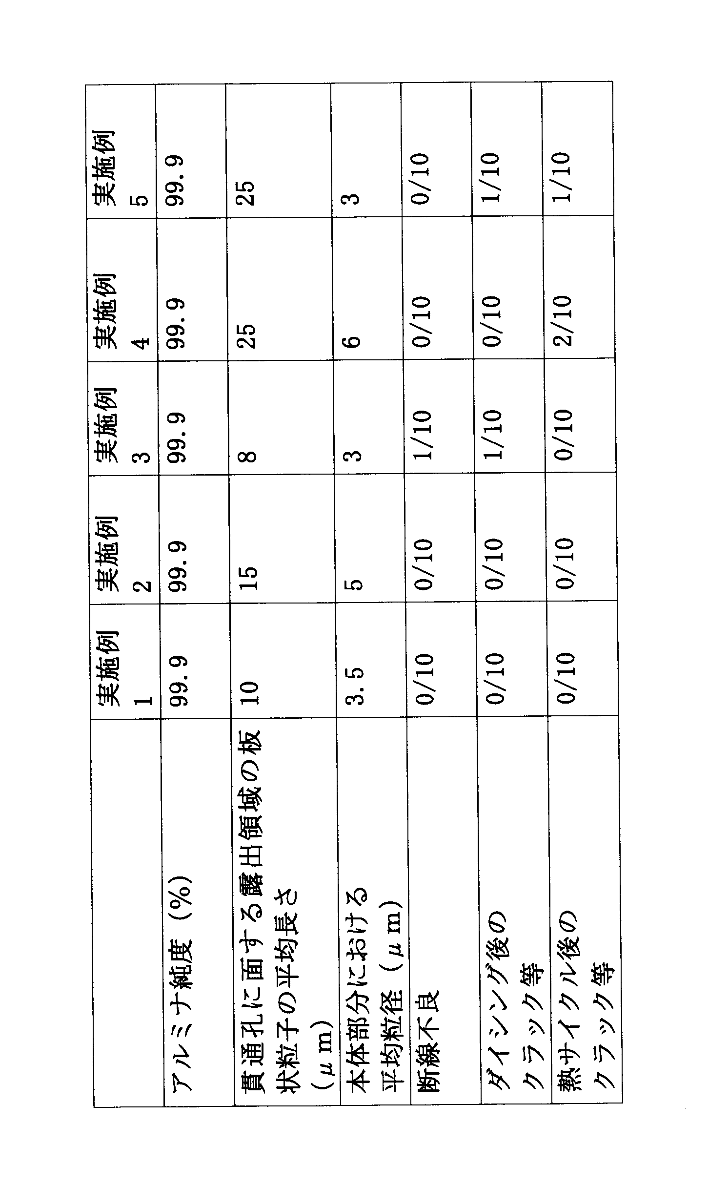

実施例では、断線不良、ダイシング後のクラックとチッピング、熱衝撃試験後のクラックとチッピングは見られないか、あるいは非常に少なかった。また、貫通孔の形状異常も見られなかった。 In the examples, disconnection defects, cracks and chipping after dicing, cracks and chipping after the thermal shock test were not observed, or very few. Further, no abnormality in the shape of the through hole was observed.
比較例1では、絶縁基板の貫通孔に面する露出領域にガラス成分が析出していた。この結果、断線不良は防止されていたが、ダイシング後のクラックとチッピング、熱衝撃試験後のクラックとチッングが多かった。 In Comparative Example 1, a glass component was deposited in an exposed region facing the through hole of the insulating substrate. As a result, disconnection failure was prevented, but there were many cracks and chipping after dicing and cracks and chipping after the thermal shock test.
比較例2では、露出領域における板状粒子の平均長さが6μmと小さいが、断線不良、ダイシング後のクラックが多い。
比較例3では、露出領域における板状粒子の平均長さが30μmであり、本体部分における平均粒径が8μmであるが、ダイシング後のクラック、熱サイクル後のクラックが多い。
比較例4では、本体部分における平均粒径が15μmであるが、ダイシング後のクラックとチッピングおよび熱衝撃試験後のクラックとチッピングが共に多い。
比較例5では、露出領域における平均長さが30μmであるが、熱衝撃試験後クラックが多い。
比較例6では、露出領域における板状粒子の平均長さが35μmであり、本体部分における平均粒径が2μmであるが、ダイシング後のクラックが多い。
比較例7では、アルミナ純度が98%であり、本体部分における平均粒径が1μmであるが、ダイシング後クラックが多い。
In Comparative Example 2, the average length of the plate-like particles in the exposed region is as small as 6 μm, but there are many disconnection defects and cracks after dicing.
In Comparative Example 3, the average length of the plate-like particles in the exposed region is 30 μm and the average particle size in the main body portion is 8 μm, but there are many cracks after dicing and cracks after thermal cycling.
In Comparative Example 4, the average particle size in the main body portion is 15 μm, but there are many cracks and chipping after dicing and cracks and chipping after the thermal shock test.
In Comparative Example 5, the average length in the exposed region is 30 μm, but there are many cracks after the thermal shock test.
In Comparative Example 6, the average length of the plate-like particles in the exposed region is 35 μm and the average particle size in the main body portion is 2 μm, but there are many cracks after dicing.
In Comparative Example 7, the alumina purity is 98% and the average particle size in the main body is 1 μm, but there are many cracks after dicing.
比較例8では、露出領域における板状粒子の平均長さが15μmであり、本体部分における平均粒径が8μmであるが、ダイシング後のクラック、熱サイクル後のクラックが多い。
比較例9では、露出領域における板状粒子の平均長さが15μmであり、本体部分における平均粒径が1μmであるが、ダイシング後のクラックが多い。
比較例10では、露出領域における板状粒子の平均長さが6μmであり、本体部分における平均粒径が5μmであるが、断線不良が多い。
In Comparative Example 8, the average length of the plate-like particles in the exposed region is 15 μm and the average particle size in the main body portion is 8 μm, but there are many cracks after dicing and cracks after thermal cycling.
In Comparative Example 9, the average length of the plate-like particles in the exposed region is 15 μm and the average particle size in the main body portion is 1 μm, but there are many cracks after dicing.
In Comparative Example 10, the average length of the plate-like particles in the exposed region is 6 μm and the average particle size in the main body portion is 5 μm, but there are many disconnections.
Claims (5)
前記絶縁基板の厚さが25~100μmであり、前記貫通孔の径が20μm~100μmであり、前記絶縁基板が、本体部分と、前記貫通孔に露出する露出領域とを備えており、前記絶縁基板がアルミナ焼結体からなり、前記アルミナ焼結体の相対密度が99.5%以上であり、前記アルミナ焼結体の純度が99.9%以上であり、前記本体部分における前記アルミナ焼結体の平均粒径が3~6μmであり、前記露出領域における前記アルミナ焼結体を構成するアルミナ粒子が板状をなしており、板状の前記アルミナ粒子の平均長さが8~25μmであることを特徴とする、貫通孔を有する絶縁基板。 An insulating substrate in which through holes for conductors are arranged,
The insulating substrate has a thickness of 25 to 100 μm, the diameter of the through hole is 20 μm to 100 μm, the insulating substrate includes a main body portion and an exposed region exposed to the through hole, The substrate is made of an alumina sintered body, the relative density of the alumina sintered body is 99.5% or more, the purity of the alumina sintered body is 99.9% or more, and the alumina sintered body in the main body portion. The average particle size of the body is 3 to 6 μm, the alumina particles constituting the alumina sintered body in the exposed region have a plate shape, and the average length of the plate-like alumina particles is 8 to 25 μm. An insulating substrate having a through hole.
Priority Applications (5)
| Application Number | Priority Date | Filing Date | Title |
|---|---|---|---|
| EP15754711.8A EP3113586B1 (en) | 2014-02-26 | 2015-02-20 | Insulating substrate having through-holes |
| CN201580000543.6A CN105144851B (en) | 2014-02-26 | 2015-02-20 | Insulating substrate with through holes |
| KR1020157023832A KR102250469B1 (en) | 2014-02-26 | 2015-02-20 | Insulating substrates including through holes |
| JP2015536336A JP5877932B1 (en) | 2014-02-26 | 2015-02-20 | Insulating substrate having a through hole |
| US14/855,798 US9538653B2 (en) | 2014-02-26 | 2015-09-16 | Insulating substrates including through holes |
Applications Claiming Priority (2)
| Application Number | Priority Date | Filing Date | Title |
|---|---|---|---|
| JP2014-035399 | 2014-02-26 | ||
| JP2014035399 | 2014-02-26 |
Related Child Applications (1)
| Application Number | Title | Priority Date | Filing Date |
|---|---|---|---|
| US14/855,798 Continuation US9538653B2 (en) | 2014-02-26 | 2015-09-16 | Insulating substrates including through holes |
Publications (1)
| Publication Number | Publication Date |
|---|---|
| WO2015129574A1 true WO2015129574A1 (en) | 2015-09-03 |
Family
ID=54008894
Family Applications (2)
| Application Number | Title | Priority Date | Filing Date |
|---|---|---|---|
| PCT/JP2015/054765 Ceased WO2015129574A1 (en) | 2014-02-26 | 2015-02-20 | Insulating substrate having through-hole |
| PCT/JP2015/055258 Ceased WO2015129699A1 (en) | 2014-02-26 | 2015-02-24 | Insulating substrate having through-hole |
Family Applications After (1)
| Application Number | Title | Priority Date | Filing Date |
|---|---|---|---|
| PCT/JP2015/055258 Ceased WO2015129699A1 (en) | 2014-02-26 | 2015-02-24 | Insulating substrate having through-hole |
Country Status (7)
| Country | Link |
|---|---|
| US (2) | US9894763B2 (en) |
| EP (2) | EP3113586B1 (en) |
| JP (2) | JP5877932B1 (en) |
| KR (2) | KR102250469B1 (en) |
| CN (2) | CN105144851B (en) |
| TW (2) | TWI632836B (en) |
| WO (2) | WO2015129574A1 (en) |
Cited By (1)
| Publication number | Priority date | Publication date | Assignee | Title |
|---|---|---|---|---|
| JP2025022755A (en) * | 2023-08-03 | 2025-02-14 | 日本特殊陶業株式会社 | Alumina sintered body and electrostatic chuck |
Families Citing this family (5)
| Publication number | Priority date | Publication date | Assignee | Title |
|---|---|---|---|---|
| WO2015129574A1 (en) * | 2014-02-26 | 2015-09-03 | 日本碍子株式会社 | Insulating substrate having through-hole |
| CN108886870B (en) * | 2016-03-11 | 2021-03-09 | 日本碍子株式会社 | Connection substrate |
| JP6470878B1 (en) * | 2017-06-13 | 2019-02-13 | 日本碍子株式会社 | Components for semiconductor manufacturing equipment |
| JP6600106B2 (en) * | 2017-06-29 | 2019-10-30 | 京セラ株式会社 | Alumina substrate and resistor using the same |
| CN118248562B (en) * | 2024-03-29 | 2025-02-11 | 江苏富乐华功率半导体研究院有限公司 | Surface treatment process of through-hole thin film ceramic substrate |
Citations (10)
| Publication number | Priority date | Publication date | Assignee | Title |
|---|---|---|---|---|
| JPH02205094A (en) * | 1989-02-03 | 1990-08-14 | Mitsubishi Mining & Cement Co Ltd | Film circuit board for micro wave |
| JPH0412936B2 (en) | 1983-04-28 | 1992-03-06 | Nitta Gelatin Kk | |
| JPH06157132A (en) | 1992-11-13 | 1994-06-03 | Toshiba Ceramics Co Ltd | High purity alumina ceramics and production thereof |
| JP2000223810A (en) * | 1999-02-01 | 2000-08-11 | Kyocera Corp | Ceramic substrate and method of manufacturing the same |
| JP2001064075A (en) | 1999-08-30 | 2001-03-13 | Sumitomo Chem Co Ltd | Translucent alumina sintered body and method for producing the same |
| JP2001199761A (en) | 2000-01-13 | 2001-07-24 | Konoshima Chemical Co Ltd | High purity alumina ceramics and method for producing the same |
| JP2003095730A (en) | 2001-09-18 | 2003-04-03 | Toshiba Ceramics Co Ltd | High-purity alumina ceramics and method for producing the same |
| JP2008244057A (en) * | 2007-03-27 | 2008-10-09 | Tdk Corp | Manufacturing method of multi-layered ceramics substrate |
| JP2013232546A (en) | 2012-04-27 | 2013-11-14 | Seiko Epson Corp | Base substrate, electronic device, and method for manufacturing base substrate |
| JP2014057124A (en) | 2012-09-11 | 2014-03-27 | Panasonic Corp | Surface acoustic wave device and manufacturing method thereof |
Family Cites Families (29)
| Publication number | Priority date | Publication date | Assignee | Title |
|---|---|---|---|---|
| JPS62260766A (en) * | 1986-05-08 | 1987-11-13 | 東レ株式会社 | Alumina sintered body |
| JP2555285B2 (en) | 1987-06-20 | 1996-11-20 | 株式会社アテックス | Grain export device for grain container |
| JPH01199921A (en) | 1988-02-03 | 1989-08-11 | Chiyoda Corp | Adsorption separation method for 2,6-diisopropylnaphthalene |
| JPH03177376A (en) * | 1989-12-04 | 1991-08-01 | Japan Gore Tex Inc | Ceramic board |
| JPH0567026A (en) | 1991-09-10 | 1993-03-19 | Shikoku Nippon Denki Software Kk | Peripheral equipment controller |
| JPH0567026U (en) | 1992-02-06 | 1993-09-03 | 株式会社三協精機製作所 | Through electrode of substrate |
| GB9526343D0 (en) * | 1995-12-22 | 1996-02-21 | Cohen A N | Improved sintered material |
| JP3411143B2 (en) * | 1995-12-28 | 2003-05-26 | 京セラ株式会社 | Metallized composition and wiring board using the same |
| EP1065190A3 (en) * | 1999-06-29 | 2001-05-16 | Hitachi Metals, Ltd. | Alumina ceramic composition |
| US6391082B1 (en) * | 1999-07-02 | 2002-05-21 | Holl Technologies Company | Composites of powdered fillers and polymer matrix |
| JP3924406B2 (en) * | 1999-09-30 | 2007-06-06 | 京セラ株式会社 | Alumina sintered body and manufacturing method thereof, wiring board and manufacturing method thereof |
| JP3898400B2 (en) * | 1999-11-26 | 2007-03-28 | 京セラ株式会社 | Wiring board and manufacturing method thereof |
| US6759740B2 (en) * | 2001-03-30 | 2004-07-06 | Kyocera Corporation | Composite ceramic board, method of producing the same, optical/electronic-mounted circuit substrate using said board, and mounted board equipped with said circuit substrate |
| CA2552908C (en) | 2004-08-06 | 2010-07-20 | A. L. M. T. Corp. | Collective substrate, semiconductor element mount, semiconductor device, imaging device, light emitting diode component and light emitting diode |
| JP4559936B2 (en) * | 2004-10-21 | 2010-10-13 | アルプス電気株式会社 | Electroless plating method and circuit forming method using this method |
| US7088000B2 (en) * | 2004-11-10 | 2006-08-08 | International Business Machines Corporation | Method and structure to wire electronic devices |
| KR101066322B1 (en) * | 2005-11-21 | 2011-09-20 | 닛뽕 카바이도 고교 가부시키가이샤 | Method for manufacturing light reflecting material, light emitting element accommodating package, light emitting device and light emitting element accommodating package |
| JP5086690B2 (en) * | 2007-05-18 | 2012-11-28 | 日本特殊陶業株式会社 | Manufacturing method of ceramic substrate |
| JP5230992B2 (en) | 2007-10-25 | 2013-07-10 | 新光電気工業株式会社 | Manufacturing method of substrate with through electrode |
| JP2009200356A (en) * | 2008-02-22 | 2009-09-03 | Tdk Corp | Printed wiring board and manufacturing method therefor |
| US20090308646A1 (en) * | 2008-06-12 | 2009-12-17 | Seiko Epson Corporation | Conductor pattern forming ink, conductor pattern, and wiring substrate |
| JP5065494B2 (en) | 2008-08-27 | 2012-10-31 | セイコーインスツル株式会社 | Piezoelectric vibrator, oscillator, electronic device, radio timepiece, and method of manufacturing piezoelectric vibrator |
| JP5017298B2 (en) * | 2009-03-11 | 2012-09-05 | 株式会社日本自動車部品総合研究所 | Alumina sintered body, manufacturing method thereof, and spark plug using the same |
| US8829355B2 (en) | 2009-03-27 | 2014-09-09 | Ibiden Co., Ltd. | Multilayer printed wiring board |
| GB201005457D0 (en) * | 2010-03-31 | 2010-05-19 | Isis Innovation | Ceramic materials |
| JP5693940B2 (en) * | 2010-12-13 | 2015-04-01 | 株式会社トクヤマ | Ceramic via substrate, metallized ceramic via substrate, and manufacturing method thereof |
| US9320155B2 (en) * | 2012-04-27 | 2016-04-19 | Panasonic Intellectual Property Management Co., Ltd. | Ceramic substrate composite and method for manufacturing ceramic substrate composite |
| JP3183661U (en) * | 2013-03-13 | 2013-05-30 | 西村陶業株式会社 | Terminal fixing structure and LED module |
| WO2015129574A1 (en) * | 2014-02-26 | 2015-09-03 | 日本碍子株式会社 | Insulating substrate having through-hole |
-
2015
- 2015-02-20 WO PCT/JP2015/054765 patent/WO2015129574A1/en not_active Ceased
- 2015-02-20 JP JP2015536336A patent/JP5877932B1/en not_active Expired - Fee Related
- 2015-02-20 CN CN201580000543.6A patent/CN105144851B/en not_active Expired - Fee Related
- 2015-02-20 KR KR1020157023832A patent/KR102250469B1/en not_active Expired - Fee Related
- 2015-02-20 EP EP15754711.8A patent/EP3113586B1/en not_active Not-in-force
- 2015-02-24 EP EP15750613.0A patent/EP3113585B1/en not_active Not-in-force
- 2015-02-24 WO PCT/JP2015/055258 patent/WO2015129699A1/en not_active Ceased
- 2015-02-24 KR KR1020157023831A patent/KR102250468B1/en not_active Expired - Fee Related
- 2015-02-24 JP JP2015536337A patent/JP5877933B1/en not_active Expired - Fee Related
- 2015-02-24 CN CN201580000703.7A patent/CN105191511B/en not_active Expired - Fee Related
- 2015-02-25 TW TW104105989A patent/TWI632836B/en not_active IP Right Cessation
- 2015-02-26 TW TW104106175A patent/TWI632124B/en not_active IP Right Cessation
- 2015-08-17 US US14/827,456 patent/US9894763B2/en active Active
- 2015-09-16 US US14/855,798 patent/US9538653B2/en not_active Expired - Fee Related
Patent Citations (10)
| Publication number | Priority date | Publication date | Assignee | Title |
|---|---|---|---|---|
| JPH0412936B2 (en) | 1983-04-28 | 1992-03-06 | Nitta Gelatin Kk | |
| JPH02205094A (en) * | 1989-02-03 | 1990-08-14 | Mitsubishi Mining & Cement Co Ltd | Film circuit board for micro wave |
| JPH06157132A (en) | 1992-11-13 | 1994-06-03 | Toshiba Ceramics Co Ltd | High purity alumina ceramics and production thereof |
| JP2000223810A (en) * | 1999-02-01 | 2000-08-11 | Kyocera Corp | Ceramic substrate and method of manufacturing the same |
| JP2001064075A (en) | 1999-08-30 | 2001-03-13 | Sumitomo Chem Co Ltd | Translucent alumina sintered body and method for producing the same |
| JP2001199761A (en) | 2000-01-13 | 2001-07-24 | Konoshima Chemical Co Ltd | High purity alumina ceramics and method for producing the same |
| JP2003095730A (en) | 2001-09-18 | 2003-04-03 | Toshiba Ceramics Co Ltd | High-purity alumina ceramics and method for producing the same |
| JP2008244057A (en) * | 2007-03-27 | 2008-10-09 | Tdk Corp | Manufacturing method of multi-layered ceramics substrate |
| JP2013232546A (en) | 2012-04-27 | 2013-11-14 | Seiko Epson Corp | Base substrate, electronic device, and method for manufacturing base substrate |
| JP2014057124A (en) | 2012-09-11 | 2014-03-27 | Panasonic Corp | Surface acoustic wave device and manufacturing method thereof |
Non-Patent Citations (1)
| Title |
|---|
| See also references of EP3113586A4 |
Cited By (2)
| Publication number | Priority date | Publication date | Assignee | Title |
|---|---|---|---|---|
| JP2025022755A (en) * | 2023-08-03 | 2025-02-14 | 日本特殊陶業株式会社 | Alumina sintered body and electrostatic chuck |
| JP7787945B2 (en) | 2023-08-03 | 2025-12-17 | 日本特殊陶業株式会社 | Alumina sintered body and electrostatic chuck |
Also Published As
| Publication number | Publication date |
|---|---|
| EP3113585B1 (en) | 2018-11-28 |
| CN105144851A (en) | 2015-12-09 |
| KR102250469B1 (en) | 2021-05-12 |
| WO2015129699A1 (en) | 2015-09-03 |
| CN105191511B (en) | 2019-04-09 |
| US9538653B2 (en) | 2017-01-03 |
| JPWO2015129699A1 (en) | 2017-03-30 |
| EP3113585A4 (en) | 2017-10-25 |
| TW201546019A (en) | 2015-12-16 |
| US20160007461A1 (en) | 2016-01-07 |
| US20150353428A1 (en) | 2015-12-10 |
| EP3113585A1 (en) | 2017-01-04 |
| CN105144851B (en) | 2019-02-12 |
| TWI632124B (en) | 2018-08-11 |
| EP3113586A4 (en) | 2017-10-25 |
| EP3113586B1 (en) | 2018-11-28 |
| TW201547334A (en) | 2015-12-16 |
| JP5877932B1 (en) | 2016-03-08 |
| TWI632836B (en) | 2018-08-11 |
| CN105191511A (en) | 2015-12-23 |
| KR20160124650A (en) | 2016-10-28 |
| KR102250468B1 (en) | 2021-05-12 |
| KR20160124649A (en) | 2016-10-28 |
| US9894763B2 (en) | 2018-02-13 |
| JPWO2015129574A1 (en) | 2017-03-30 |
| JP5877933B1 (en) | 2016-03-08 |
| EP3113586A1 (en) | 2017-01-04 |
Similar Documents
| Publication | Publication Date | Title |
|---|---|---|
| JP5877932B1 (en) | Insulating substrate having a through hole | |
| KR101142000B1 (en) | Electrostatic chuck | |
| JP5396353B2 (en) | Electrostatic chuck and manufacturing method thereof | |
| JP6076486B2 (en) | Handle substrate for composite substrates for semiconductors | |
| JP2004260039A (en) | Holder for semiconductor or liquid crystal manufacturing apparatus and semiconductor or liquid crystal manufacturing apparatus equipped with the same | |
| JP5697813B1 (en) | Handle substrate for composite substrates for semiconductors | |
| JPWO2017154593A1 (en) | Connection board | |
| WO2014174946A1 (en) | Handle substrate for composite substrate for semiconductor | |
| JP5849176B1 (en) | Handle substrate for composite substrate for semiconductor and composite substrate for semiconductor | |
| WO2017154422A1 (en) | Connection substrate | |
| JP2004273659A (en) | Wafer holder for semiconductor manufacturing apparatus and semiconductor manufacturing apparatus equipped with the same | |
| JP2017109895A (en) | Method for producing ceramic sintered body |
Legal Events
| Date | Code | Title | Description |
|---|---|---|---|
| WWE | Wipo information: entry into national phase |
Ref document number: 201580000543.6 Country of ref document: CN |
|
| ENP | Entry into the national phase |
Ref document number: 2015536336 Country of ref document: JP Kind code of ref document: A |
|
| ENP | Entry into the national phase |
Ref document number: 20157023832 Country of ref document: KR Kind code of ref document: A |
|
| REEP | Request for entry into the european phase |
Ref document number: 2015754711 Country of ref document: EP |
|
| WWE | Wipo information: entry into national phase |
Ref document number: 2015754711 Country of ref document: EP |
|
| 121 | Ep: the epo has been informed by wipo that ep was designated in this application |
Ref document number: 15754711 Country of ref document: EP Kind code of ref document: A1 |
|
| NENP | Non-entry into the national phase |
Ref country code: DE |