WO2015092840A1 - Organic light-emitting element - Google Patents
Organic light-emitting element Download PDFInfo
- Publication number
- WO2015092840A1 WO2015092840A1 PCT/JP2013/083544 JP2013083544W WO2015092840A1 WO 2015092840 A1 WO2015092840 A1 WO 2015092840A1 JP 2013083544 W JP2013083544 W JP 2013083544W WO 2015092840 A1 WO2015092840 A1 WO 2015092840A1
- Authority
- WO
- WIPO (PCT)
- Prior art keywords
- light emitting
- transport layer
- group
- dopant
- organic light
- Prior art date
- Legal status (The legal status is an assumption and is not a legal conclusion. Google has not performed a legal analysis and makes no representation as to the accuracy of the status listed.)
- Ceased
Links
Images

Classifications
-
- H—ELECTRICITY
- H10—SEMICONDUCTOR DEVICES; ELECTRIC SOLID-STATE DEVICES NOT OTHERWISE PROVIDED FOR
- H10K—ORGANIC ELECTRIC SOLID-STATE DEVICES
- H10K50/00—Organic light-emitting devices
- H10K50/10—OLEDs or polymer light-emitting diodes [PLED]
- H10K50/11—OLEDs or polymer light-emitting diodes [PLED] characterised by the electroluminescent [EL] layers
- H10K50/125—OLEDs or polymer light-emitting diodes [PLED] characterised by the electroluminescent [EL] layers specially adapted for multicolour light emission, e.g. for emitting white light
-
- H—ELECTRICITY
- H10—SEMICONDUCTOR DEVICES; ELECTRIC SOLID-STATE DEVICES NOT OTHERWISE PROVIDED FOR
- H10K—ORGANIC ELECTRIC SOLID-STATE DEVICES
- H10K50/00—Organic light-emitting devices
- H10K50/10—OLEDs or polymer light-emitting diodes [PLED]
- H10K50/14—Carrier transporting layers
- H10K50/15—Hole transporting layers
- H10K50/155—Hole transporting layers comprising dopants
-
- H—ELECTRICITY
- H10—SEMICONDUCTOR DEVICES; ELECTRIC SOLID-STATE DEVICES NOT OTHERWISE PROVIDED FOR
- H10K—ORGANIC ELECTRIC SOLID-STATE DEVICES
- H10K50/00—Organic light-emitting devices
- H10K50/10—OLEDs or polymer light-emitting diodes [PLED]
- H10K50/14—Carrier transporting layers
- H10K50/16—Electron transporting layers
- H10K50/165—Electron transporting layers comprising dopants
-
- H—ELECTRICITY
- H10—SEMICONDUCTOR DEVICES; ELECTRIC SOLID-STATE DEVICES NOT OTHERWISE PROVIDED FOR
- H10K—ORGANIC ELECTRIC SOLID-STATE DEVICES
- H10K85/00—Organic materials used in the body or electrodes of devices covered by this subclass
- H10K85/30—Coordination compounds
- H10K85/341—Transition metal complexes, e.g. Ru(II)polypyridine complexes
- H10K85/342—Transition metal complexes, e.g. Ru(II)polypyridine complexes comprising iridium
Definitions
- the present invention relates to an organic light emitting device.
- the structure of the light emitting layer of the white light emitting organic LED includes a single layer structure and a laminated structure.
- Patent Document 1 reports a laminated structure in which a hole transport layer is doped with a yellow dopant and a blue dopant is contained in a light emitting layer.
- Methods of manufacturing the organic LED include a vapor deposition method and a wet method.
- the vapor deposition method as described in Patent Document 1, it is possible to form a light emitting layer having an arbitrary laminated structure.
- the deposition method has production problems such as low utilization efficiency of the material and difficulty in increasing the area.
- the wet method there are production advantages such as high utilization efficiency of materials and easy enlargement, but there is a problem that it is difficult to form a laminated structure.
- the underlayer should be insoluble in the upper layer solvent. Therefore, the range of material selection is narrow, and there is a problem that the excited state formed in the light emitting layer transfers energy to the peripheral layer to be deactivated and the light emission efficiency is lowered.
- An object of the present invention is to provide a highly efficient white organic LED that can be formed by a wet process.
- Patent Document 1 describes that the hole transport layer contains a yellow dopant, it does not clearly show how the yellow dopant is distributed in the hole transport layer, so that it is considered that the light emission efficiency is low.
- the present invention relates to a first electrode, a second electrode, a light emitting layer disposed between the first electrode and the second electrode, and a charge disposed at a position adjacent to the light emitting layer.
- An organic light emitting device having a transport layer, wherein the charge transport layer adjacent to the light emitting layer contains a light emitting dopant, and the light emitting dopant moves near the interface between the light emitting layer and the charge transport layer It is characterized by having a functional group.
- an organic light emitting element which can be formed by a wet method and which achieves high efficiency light emission.
- FIG. 1 is a cross-sectional view of an embodiment of the organic light emitting device in the present invention.
- the substrate 1 is a glass substrate.
- the present invention is not limited to the glass substrate, and a plastic substrate or a metal substrate provided with a suitable water permeability lowering protective film can also be used.
- the light extraction layer a layer having a scattering property or a layer having a microlens can be used.
- the lower electrode 2 is an anode.
- Transparent electrodes such as ITO and IZO are used.
- the invention is not limited thereto, and a laminate of Al, Ag or the like, a combination of Mo, Cr, a transparent electrode and a light diffusion layer, or the like can also be used.
- the lower electrode is not limited to the anode, and a cathode can also be used. In that case, Al, Mo, a laminate of Al and Li, an alloy such as AlNi, or the like is used.
- a transparent electrode such as ITO or IZO may be used.
- the upper electrode 8 is a cathode.
- a laminate of Al, an electron injecting LiF, a fluoride of an alkali metal such as Li20, an oxide or the like is used.
- a co-evaporation product of Al and an alkali metal is also used.
- a laminate of a transparent electrode such as ITO or IZO and an electron injecting electrode such as MgAg or Li can be used.
- MgAg or Ag thin film can be used alone.
- a buffer layer may be provided in order to reduce damage due to sputtering.
- a metal oxide such as molybdenum oxide or vanadium oxide is used.
- the lower electrode is a cathode as described above
- the upper electrode is an anode.
- a transparent electrode such as ITO or IZO is used.
- a metal thin film such as an Ag thin film can be used.
- a buffer layer may be provided in order to reduce damage caused by sputtering.
- a metal oxide such as molybdenum oxide or vanadium oxide is used.
- the hole injection layer 3 is a layer for injecting holes from the lower electrode 2.
- a single layer or a plurality of layers may be provided.
- the hole injection layer 3 is preferably a conductive polymer such as PEDOT (poly (3,4-ethylenedioxythiophene)): PSS (polystyrene sulfonate).
- PEDOT poly (3,4-ethylenedioxythiophene)
- PSS polystyrene sulfonate
- polypyrrole-based and triphenylamine-based polymer materials can be used.
- phthalocyanine compounds and starburst amine compounds which are often used in combination with a low molecular weight (weight average molecular weight of 10000 or less) material system are also applicable.
- the hole transport layer 4 is a layer that efficiently injects holes from the hole injection layer 3 into the light emitting layer and transfers energy from the light emitting layer to efficiently emit light.
- materials insoluble in the solvent of the upper layer of a homopolymer or copolymer such as fluorene, carbazole, or arylamine are used.
- materials having a thiophene type or a pyrrole type as a skeleton can also be used.
- polymers having a skeleton such as fluorene, carbazole, arylamine, thiophene or pyrrole in the side chain can also be used.
- the hole transport layer 4 of the present invention contains a light emitting dopant.
- the light emitting dopant of the present invention may be any of so-called fluorescent materials, phosphorescent materials, and delayed fluorescent materials.
- the light emitting dopant includes the functionality to be present in high concentration near the interface with the light emitting layer.
- the concentration of the light emitting dopant is not particularly limited, but preferably about 0.1 to 10 wt%.
- the light emitting layer 5 is a layer for obtaining light emission of a desired light emission color.
- the light emitting layer 5 contains a host and a light emitting dopant.
- the light emitting dopant any of so-called fluorescent materials, phosphorescent materials and delayed fluorescent materials can be used. Only one kind of light emitting dopant may be used, but two or three kinds of light emitting dopants may be used.
- the light emitting layer 5 may contain a hole transporting material or an electron transporting material in addition to the host and the light emitting dopant. They are used to improve charge balance in the light emitting layer.
- the light emitting layer 5 may contain a binder polymer.
- a triphenylamine derivative a carbazole derivative, a fluorene derivative or an arylsilane derivative
- metal complexes of 8-quinolinol can also be used.
- binder polymers such as polycarbonate, polystyrene, acrylic resin, polyamide and gelatin can also be used in combination.
- the hole blocking layer 6 is a layer for preventing transfer of holes from the light emitting layer 5 to the electron transporting layer 7.
- Examples of the material of the hole blocking layer 6 include bis (2-methyl-8-quinolinolato) -4- (phenylphenolato) aluminum (hereinafter, BAlq) and tris (8-quinolinolato) aluminum (hereinafter, Alq3).
- Tris (2,4,6-trimethyl-3- (pyridin-3-yl) phenyl) borane hereinafter, 3TPYMB
- 1,4-bis (triphenylsilyl) benzene hereinafter, UGH2
- oxadiazole derivative 1,4-bis (triphenylsilyl) benzene
- UGH2 1,4-bis (triphenylsilyl) benzene
- UGH2 1,4-bis (triphenylsilyl) benzene
- oxadiazole derivative 1,4-bis (triphenylsilyl) benzene
- triazole Derivatives fullerene derivatives, phenanthroline derivatives, quinoline derivatives, benzimidazole derivatives, triazine derivatives and the like can be used.
- the electron transport layer 7 is a layer for transporting electrons to the light emitting layer 5 via the hole blocking layer 6.
- Examples of the material of the electron transport layer 7 include bis (2-methyl-8-quinolinolato) -4- (phenylphenolato) aluminum (hereinafter, BAlq), tris (8-quinolinolato) aluminum (hereinafter, Alq3), Tris (2,4,6-trimethyl-3- (pyridin-3-yl) phenyl) borane (hereinafter, 3TPYMB), 1,4-bis (triphenylsilyl) benzene (hereinafter, UGH2), oxadiazole derivative, triazole derivative A fullerene derivative, a phenanthroline derivative, a quinoline derivative, a benzimidazole derivative, a triazine derivative or the like can be used.
- a large amount of light emitting dopant is distributed in the vicinity of the interface between the hole transport layer 4 and the light emitting layer 5. Therefore, when the excited state formed in the light emitting layer 5 transfers energy to the hole transport layer 4, a large amount of light is emitted in the vicinity of the interface with the light emitting layer 5 of the hole transport layer 4, and the transferred energy is deactivated. Prevent being lost. Further, the light emitting dopant concentration in the hole transport layer 4 is hardly present on the hole injection layer 3 side, and is high near the light emitting layer 5.
- the light emitting dopant can be a hole trap in the hole transport layer 4, but in the present invention, since it has the concentration distribution as described above, it does not become a hole trap up to the vicinity of the light emitting layer 5. Therefore, hole injection can be efficiently performed as compared with the case where the above concentration distribution is not provided.
- the hole blocking layer 6 has the light emitting dopant having a functional group to be present in the vicinity of the interface with the light emitting layer 5 in high concentration. You may Such a structure can also obtain the same effect as described above.
- At least one of the hole transport layer 4 or the electron transport layer 7 contains a light emitting dopant having a predetermined functional group.
- a light emitting dopant having a predetermined functional group there are various forms as to how many kinds of light emitting dopants are included in each of the light emitting layer 5, the hole transporting layer 4, and the electron transporting layer 7. The form is shown in Table 1.
- Table 1 shows an example in which a stacked structure is formed in the order of blue, red and green from the upper electrode 8 to the lower electrode 2.
- blue, red and green are used, it is possible to realize white light emission not only in this but also in the order of blue, green and red or in the order of red, blue and green.
- the luminous efficiency is particularly high in the order of blue, green, red, blue, red and green.
- the electron transport layer 7 does not contain a light emitting dopant
- the light emitting layer 5 contains a blue dopant and a red dopant
- the hole transport layer 4 contains a green dopant.
- the green dopant has a functional group for moving the green dopant to the vicinity of the interface between the light emitting layer 5 and the hole transport layer 4.
- fluoroalkyl group, perfluoroalkyl group and siloxy group having fluoroalkyl group can be mentioned as the functional group.
- the electron transport layer 7 contains a blue dopant
- the light emitting layer 5 contains a red dopant and a green dopant
- the hole transport layer 4 does not contain a luminescent dopant.
- the blue dopant has a functional group for moving the blue dopant to the vicinity of the interface between the electron transport layer 7 and the light emitting layer 5.
- an alkyl group having 4 or more carbon atoms, a hydroxy group, a carboxyl group, an amido group, an acyl group and an amino group can be mentioned as the functional group.
- the pattern 3 has a configuration in which the electron transport layer 7 contains a blue dopant and a red dopant, the light emitting layer 5 contains a green dopant, and the hole transport layer 4 does not contain a luminescent dopant.
- the blue dopant or the red dopant has a functional group for moving the dopant to the vicinity of the interface between the electron transport layer 7 and the light emitting layer 5.
- an alkyl group having 4 or more carbon atoms, a hydroxy group, a carboxyl group, an amido group, an acyl group and an amino group can be mentioned as the functional group.
- both the blue dopant and the red dopant may move to the vicinity of the interface between the electron transport layer 7 and the light emitting layer 5.
- the electron transport layer 7 does not contain a light emitting dopant
- the light emitting layer 5 contains a blue dopant
- the hole transport layer 4 contains a red dopant and a green dopant.
- the red dopant or the green dopant has a functional group for moving the dopant to the vicinity of the interface between the light emitting layer 5 and the hole transport layer 4.
- fluoroalkyl group, perfluoroalkyl group and siloxy group having fluoroalkyl group can be mentioned as the functional group. Note that both the red dopant and the green dopant may move to the vicinity of the interface between the light emitting layer 5 and the hole transport layer 4.
- the electron transport layer 7 contains a blue light emitting dopant
- the light emitting layer 5 contains a red dopant
- the hole transport layer 4 contains a green dopant.
- the green dopant has a functional group for moving the green dopant to the vicinity of the interface between the light emitting layer 5 and the hole transport layer 4.
- fluoroalkyl group, perfluoroalkyl group and siloxy group having fluoroalkyl group can be mentioned as the functional group.
- the blue dopant has a functional group for moving the blue dopant to the vicinity of the interface between the electron transport layer 7 and the light emitting layer 5.
- an alkyl group having 4 or more carbon atoms, a hydroxy group, a carboxyl group, an amido group, an acyl group and an amino group can be mentioned as the functional group.
- the luminous efficiency is higher if the luminous dopants of each color are present with a concentration gradient than the luminous dopants contained in the organic luminous element are collectively present in a certain region. Therefore, in the case of the pattern 5, the luminous efficiency is the highest.
- Example 1 and Comparative Example 1 In Example 1, the following materials were used for each layer.
- a glass substrate was used as the substrate 1 and ITO was used as the lower electrode 2.
- PEDOT poly (3,4-ethylenedioxythiophene)
- PSS polystyrene sulfonate
- the dopant of Formula (1) has a fluoroalkyl group. As a result, the dopant of the formula (1) spontaneously moves toward the interface between the light emitting layer 5 and the hole transport layer 4, and as a result, the concentration of the green dopant at the interface between the light emitting layer 5 and the hole transport layer 4 It gets higher locally.
- mCP 1-dicarbazolylbenzene
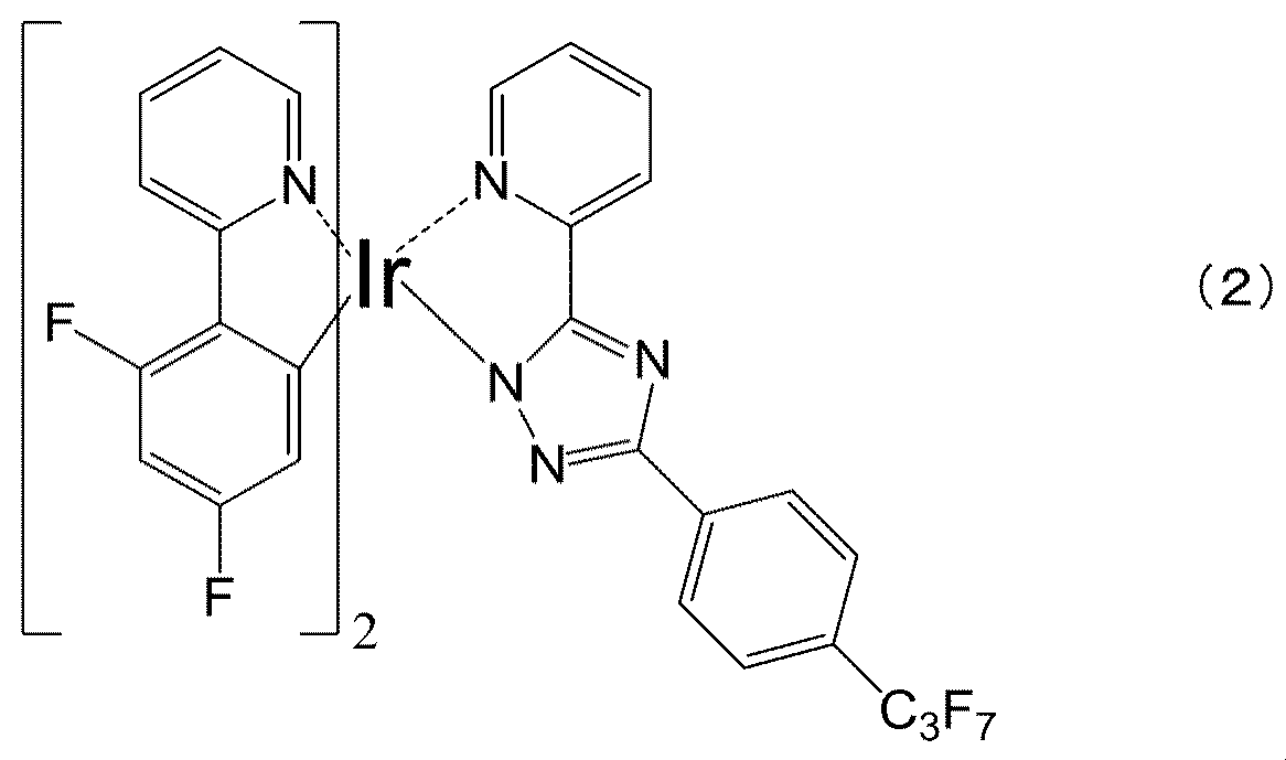
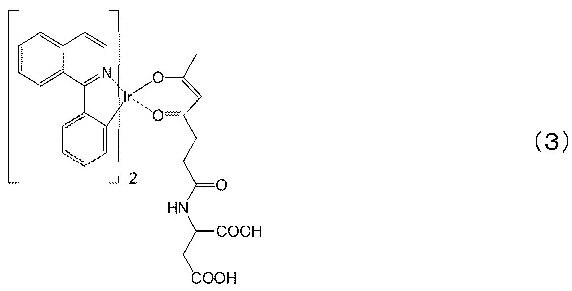
- the blue dopant of the following formula (2) and the red dopant of Formula (3) were used for the dopant.
- the blue dopant and the green dopant are 1% by weight with respect to the host.
- the coating liquid for forming the light emitting layer 5 was prepared using toluene as a solvent so that the weight ratio of solid content to the solvent was 1%.
- the light emitting layer 5 was formed by spin coating using this coating solution.
- Comparative Example 1 an organic light emitting device was produced as a structure similar to that of Example 1 except for the following points.
- the hole transport layer 4 does not have a light emitting dopant. Only the triphenylamine-based polymer of Example 1 is used. Further, the light emitting layer 5 has a green light emitting dopant represented by the following formula (4).
- Example 1 A voltage was applied to the organic light emitting devices manufactured in Example 1 and Comparative Example 1, and the current and luminance flowing were measured.
- the maximum power efficiency of the organic light emitting device of Example 1 determined from the result was 1.4 times that of the organic light emitting device of Comparative Example 1.
- the power efficiency of the organic light emitting device of Example 1 is increased compared to the organic light emitting device of Comparative Example 1 because the blue dopant and the red dopant are excited in the light emitting layer 5 of Example 1. Thereafter, the excitation energy of the blue dopant transferred to the hole transport layer 4 contributes to the light emission of the green dopant in the hole transport layer 4, and the green dopant efficiently emits light.
- Example 2 and Comparative Example 2 The structure of the organic light emitting device of Example 2 is the same as that of Example 1 except for the following.
- the hole transport layer 4 does not have a light emitting dopant. Only the triphenylamine-based polymer of Example 1 is used.
- the host material of the light emitting layer 5 used the material represented by Formula (5).
- the light emitting dopant represented by the formula (1) was used.
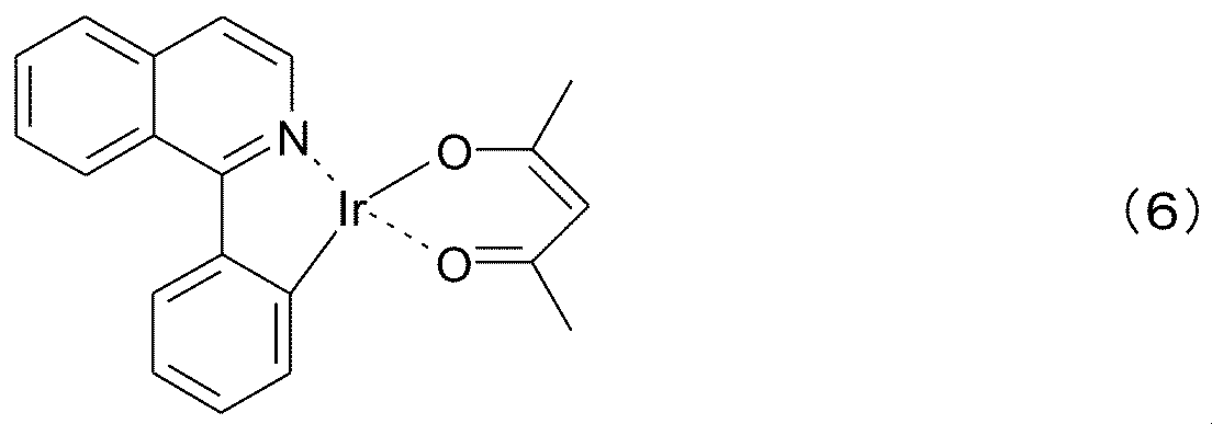
- red dopant present in the light emitting layer 5 a light emitting dopant represented by the formula (6) was used.
- the electron transport layer 7 is composed of a host and a light emitting dopant, and the material represented by the formula (7) is used as the host, and the material represented by the formula (8) is used as the light emitting dopant.
- the concentration of the light emitting dopant is 3 wt% with respect to the host.
- An isopropyl alcohol was used as the solvent, and a solution having a total solid content of 1 wt% was used to form a film on the light emitting layer by spin coating.
- the structure of the organic light emitting device of Comparative Example 2 is the same as that of Example 2 except for the following.
- the electron transport layer 7 does not contain a light emitting dopant. It is only the host material represented by Formula (7).
- the light emitting layer 5 contains 3 wt% of the light emitting dopant represented by the formula (8) with respect to the host.
- a voltage was applied to the organic light emitting device produced in Example 2 and Comparative Example 2, and the current and luminance flowing were measured. As a result, the maximum power efficiency of Example 2 was 1.4 times that of Comparative Example 2.
- the efficiency of the organic light emitting device of Example 2 is large compared to the organic light emitting device of Comparative Example 2 because the exciton formed at the interface between the light emitting layer 5 and the electron transporting layer 7 of Example 2 emits light. This is to contribute to the emission of the green dopant and the red dopant in the layer and to contribute to the emission of the blue dopant without moving to the electron transport layer 7 and quenching.
- Example 3 The organic light emitting device of Example 3 has the same configuration as the organic light emitting device of Example 1 except for the following.
- the dopant represented by Formula (4) was used for the hole transport layer 4 of a present Example. Unlike the formula (1), the dopant of the formula (4) does not have a fluoroalkyl group.
- the characteristics of the organic light emitting device of this example were measured in the same manner as in Example 1. As a result, the maximum power efficiency of the organic light emitting device of this example was 1.2 times that of Comparative Example 1.
- the efficiency of the organic light emitting device of Example 3 is large compared to the organic light emitting device of Comparative Example 1 because the blue dopant and the red dopant become excited in the light emitting layer 5 of Example 3, and thereafter This is because the excitation energy of the blue dopant transferred to the hole transport layer 4 contributes to the emission of the green dopant in the hole transport layer 4 and the green dopant efficiently emits light.
- Example 4 the reason that the efficiency of the organic light emitting device of Example 3 is small compared to the organic light emitting device of Example 1 is that the green dopant of Example 3 does not have a fluoroalkyl group. It is distributed throughout, and as a result, the green dopant acts as a hole trap in the hole transport layer 4 to prevent the hole transport.
- Example 4 and Comparative Example 3 The organic light-emitting device of Example 4 has the same configuration as that of Example 1 except for the following. For the hole transport layer 4, a light emitting dopant represented by the formula (9) was used.
- a carbazole-based material which is crosslinked by heating to be insolubilized was used as a host material of the hole transport layer 4.
- This material contains an acid generator to initiate a crosslinking reaction upon heating.
- the hole transport layer 4 was formed into a film by spin coating from a toluene solution having a solid content of 1 wt%, and was heated at 180 ° C. for 30 minutes to be crosslinked and inactivated.
- the organic light emitting device of Comparative Example 3 has the same configuration as the organic light emitting device of Example 4 except for the following. That is, the material represented by Formula (1) was used as a light emitting dopant of the hole transport layer 4. As a result, the maximum power efficiency of the organic light emitting device of Example 4 was 1.6 times that of the organic light emitting device of Comparative Example 3.
- Example 4 H + generated from the acid generating material This is because ions are added to the unpaired electron of the N atom of the amide bond contained in the light emitting dopant represented by the formula (9) to prevent the decomposition of the light emitting dopant.
- the light emitting dopant contains an element having an unpaired electron
- the light emission efficiency is improved.
- Table 2 shows the configurations of Example 1-4 and Comparative example 1-3.
Landscapes
- Physics & Mathematics (AREA)
- Optics & Photonics (AREA)
- Electroluminescent Light Sources (AREA)
Abstract
Description
本発明は、有機発光素子に関する。 The present invention relates to an organic light emitting device.
白色発光の有機LED(有機発光ダイオード)の発光層の構造には、単層構造と積層構造がある。積層構造の例として、正孔輸送層に黄色ドーパントをドープし、青色ドーパントを発光層に有する積層構造が特許文献1にて報告されている。
The structure of the light emitting layer of the white light emitting organic LED (organic light emitting diode) includes a single layer structure and a laminated structure. As an example of a laminated structure,
有機LEDの製造方法には、蒸着法と湿式法がある。蒸着法では特許文献1にあるように、任意な積層構造の発光層を形成することができる。しかし、蒸着法には、材料の利用効率が低い、大面積化がむずかしいなどの生産上の課題がある。湿式法では、材料の利用効率が高い、大面積化が容易であるなどの生産上の利点があるが、積層構造を形成することがむずかしいという課題がある。湿式法で積層した場合、下地層は上層の溶媒に対して不溶でなければならない。そのため材料選択の幅が狭く、発光層で形成された励起状態が周辺層にエネルギー移動して失活し、発光効率を低下してしまう課題があった。本発明の目的は、湿式法で形成できる、高効率な白色有機LEDを提供することである。
Methods of manufacturing the organic LED include a vapor deposition method and a wet method. In the vapor deposition method, as described in
なお、特許文献1には正孔輸送層に黄色ドーパントを含む記載があるが、黄色ドーパントが正孔輸送層内でどのように分布するのか明示していないので、発光効率が低いと考えられる。
Although
上記課題を解決するための本発明の特徴は以下の通りである。本発明は、第一の電極と、第二の電極と、前記第一の電極と前記第二の電極との間に配置された発光層と、前記発光層と隣接する位置に配置された電荷輸送層と、を有する有機発光素子であって、前記発光層に隣接する電荷輸送層には発光ドーパントを含み、前記発光ドーパントは、前記発光層と前記電荷輸送層の界面近傍に移動するための機能性基を有することを特徴とする。 The features of the present invention for solving the above problems are as follows. The present invention relates to a first electrode, a second electrode, a light emitting layer disposed between the first electrode and the second electrode, and a charge disposed at a position adjacent to the light emitting layer. An organic light emitting device having a transport layer, wherein the charge transport layer adjacent to the light emitting layer contains a light emitting dopant, and the light emitting dopant moves near the interface between the light emitting layer and the charge transport layer It is characterized by having a functional group.
本発明により、湿式法で形成できる、高効率発光を実現した有機発光素子を提供できる。上記した以外の課題、構成及び効果は以下の実施形態の説明により明らかにされる。 According to the present invention, it is possible to provide an organic light emitting element which can be formed by a wet method and which achieves high efficiency light emission. Problems, configurations, and effects other than those described above will be apparent from the description of the embodiments below.
以下、図面等により本発明を詳細に説明する。 Hereinafter, the present invention will be described in detail with reference to the drawings and the like.
図1は本発明における有機発光素子の一実施の形態における断面図である。 FIG. 1 is a cross-sectional view of an embodiment of the organic light emitting device in the present invention.
基板1はガラス基板である。但し、ガラス基板に限るものではなく、適切な透水性低下保護膜を施したプラスティック基板や金属基板も用いることができる。また、光取出し層を有していてもよい。光取出し層には散乱性を有する層やマイクロレンズを有する層を用いることができる。
The
下部電極2は陽極である。ITO,IZOなどの透明電極が用いられる。但し、それらに限られるものではなく、Al,Agなどの積層体やMo,Crや透明電極と光拡散層との組合せなども用いることができる。また、下部電極は陽極に限るものではなく、陰極も用いることができる。その場合はAl、Mo,やAlとLiの積層体やAlNiなどの合金などが用いられる。また、ITO,IZOなどの透明電極を用いてもよい。
The
上部電極8は陰極である。Alと電子注入性のLiF、Li20などのアルカリ金属のフッ化物、酸化物などの積層体が用いられる。また、Alとアルカリ金属の共蒸着物も用いられる。またITO,IZOなどの透明電極とMgAg、Liなどの電子注入性電極の積層体を用いることもできる。但し、それらに限られるものではなく、MgAgやAg薄膜単独でも用いることができる。また、ITO,IZOをスパッタ法で形成する際には、スパッタによるダメージを緩和するため、バッファー層を設けることがある。バッファー層には、酸化モリブデン、酸化バナジウムなどの金属酸化物を用いる。上記のように下部電極が陰極となる場合には、上部電極は陽極となる。その場合には、ITO,IZOなどの透明電極が用いられる。また、Ag薄膜などの金属薄膜を用いることができる。ITO,IZOなどの透明電極をスパッタ法で形成する際には、スパッタによるダメージを緩和するため、バッファー層を設けることがある。バッファー層には、酸化モリブデン、酸化バナジウムなどの金属酸化物を用いる。
The
正孔注入層3は下部電極2から正孔を注入するための層である。単層もしくは複数層設けてもよい。正孔注入層3としては、PEDOT(ポリ(3、4-エチレンジオキシチオフェン)):PSS(ポリスチレンスルホネート)等の導電性高分子が好ましい。その他にも、ポリピロール系やトリフェニルアミン系のポリマー材料を用いることができる。また、低分子(重量平均分子量10000以下)材料系と組合せてよく用いられる、フタロシアニン類化合物やスターバーストアミン系化合物も適用可能である。
The
正孔輸送層4は正孔注入層3から発光層に効率よく正孔を注入し、かつ発光層からエネルギー移動して効率よく発光する層である。正孔輸送層としては、フルオレン、カルバゾール、アリールアミンなどの単独あるいは共重合体の上層の溶媒に不溶な材料が用いられる。共重合体としては、チオフェン系、ピロール系を骨格に有する材料でも用いることができる。また、側鎖にフルオレン、カルバゾール、アリールアミン、チオフェン、ピロールなどの骨格を有するポリマーも用いることができる。また、ポリマーに限ることはなく、スターバーストアミン系化合物やアリールアミン系化合物、スチルベン誘導体、ヒドラゾン誘導体、チオフェン誘導体などのうち、上層の溶媒に不溶な材料を用いることができる。また、上記の材料を含むポリマーをもちいてもよい。また、これらの材料に限られるものではなく、これらの材料を2種以上併用しても差し支えない。また、本発明の正孔輸送層4には発光ドーパントが含まれる。本発明の発光ドーパントは、いわゆる蛍光材料、燐光材料、遅延蛍光材料のいずれでもよい。発光ドーパントには発光層との界面近傍に高濃度で存在するための機能性が含まれている。発光ドーパントの濃度には特に制約はないが、0.1から10wt%程度がのぞましい。
The
発光層5は所望の発光色の発光を得るための層である。発光層5はホスト及び発光ドーパントを含む。発光ドーパントとして、いわゆる蛍光材料、燐光材料、遅延蛍光材料のいずれでも用いることができる。発光ドーパントは1種類だけでもよいが、2種類、3種類を用いてもよい。2種類、3種類を混合して白色は発光させる場合には、発光層5はホスト、発光ドーパント以外に正孔輸送材料或いは電子輸送材料を含んでいてもよい。それらは、発光層中のチャージバランスを向上させるために用いられる。また、発光層5はバインダポリマーを含んでもよい。
The
ホストとして、トリフェニルアミン誘導体、カルバゾール誘導体、フルオレン誘導体またはアリールシラン誘導体などを用いることが好ましい。また、8-キノリノールの金属錯体なども用いることができる。また、ポリカーボネート、ポリスチレン、アクリル樹脂、ポリアミド、ゼラチンなどのバインダポリマーも合わせて用いることができる。 It is preferable to use a triphenylamine derivative, a carbazole derivative, a fluorene derivative or an arylsilane derivative as a host. In addition, metal complexes of 8-quinolinol can also be used. Further, binder polymers such as polycarbonate, polystyrene, acrylic resin, polyamide and gelatin can also be used in combination.
正孔阻止層6は正孔が発光層5から電子輸送層7に移動するのを防ぐための層である。正孔阻止層6の材料としては、例えば、ビス(2-メチル-8-キノリノラト)-4-(フェニルフェノラト)アルミニウム(以下、BAlq)や、トリス(8-キノリノラト)アルミニウム(以下、Alq3)、Tris(2、4、6-trimethyl-3-(pyridin-3-yl)phenyl)borane(以下、3TPYMB)、1、4-Bis(triphenylsilyl)benzene(以下、UGH2)、オキサジアゾール誘導体、トリアゾール誘導体、フラーレン誘導体、フェナントロリン誘導体、キノリン誘導体、ベンズイミダゾール誘導体、トリアジン誘導体等を用いることができる。
The
電子輸送層7は電子を、正孔阻止層6を介して発光層5に輸送するための層である。電子輸送層7の材料としては、例えば、ビス(2-メチル-8-キノリノラト)-4-(フェニルフェノラト)アルミニウム(以下、BAlq)や、トリス(8-キノリノラト)アルミニウム(以下、Alq3)、Tris(2、4、6-trimethyl-3-(pyridin-3-yl)phenyl)borane(以下、3TPYMB)、1、4-Bis(triphenylsilyl)benzene(以下、UGH2)、オキサジアゾール誘導体、トリアゾール誘導体、フラーレン誘導体、フェナントロリン誘導体、キノリン誘導体、ベンズイミダゾール誘導体、トリアジン誘導体等を用いることができる。
The
本発明の構造では、正孔輸送層4の発光層5との界面近傍に発光ドーパントが多く分布している。そのため、発光層5中で形成された励起状態が正孔輸送層4にエネルギー移動した際、正孔輸送層4の発光層5との界面近傍で多く発光し、移動したエネルギーが失活してロスされることを防ぐ。また、正孔輸送層4中の発光ドーパント濃度は正孔注入層3側にはほとんどなく、発光層5の近くで高い濃度になっている。発光ドーパントは正孔輸送層4中で正孔トラップとなりうるが、本発明では上記のような濃度分布を有するため、発光層5近傍までは正孔トラップとならない。そのため、上記のような濃度分布を持たない場合と比較して効率よく正孔注入を行うことができる。
In the structure of the present invention, a large amount of light emitting dopant is distributed in the vicinity of the interface between the
上記の説明では、正孔輸送層4に発光ドーパントを含む例で説明したが、正孔阻止層6に発光層5との界面近傍に高濃度で存在するための機能基を有する発光ドーパントを有してもよい。そのような構造でも上記と同様な効果を得ることができる。
<発光層5、正孔輸送層4、電子輸送層7の関係>
本発明においては、正孔輸送層4または電子輸送層7の少なくとも一方において発光層5と境界付近にの発光ドーパントが偏在することを必須の要件とする。それを実現するためには、正孔輸送層4または電子輸送層7の少なくとも一方に、所定の機能性基を有する発光ドーパントを含むことが有効である。但し、発光層5、正孔輸送層4、電子輸送層7のそれぞれに、何種類の発光ドーパントを含むかについては様々な形態がある。表1にその形態について示す。
In the above description, although the example in which the
<Relationship Between Light-Emitting
In the present invention, it is an essential requirement that at least one of the

表1では上部電極8から下部電極2に向けて、青、赤、緑の順に積層構造を形成した例である。ここでは、青、赤、緑としているが、これに限らず、青、緑、赤の順番でも、赤、青、緑の順番でも白色発光を実現することは可能である。但し、青、緑、赤や青、赤、緑の順番が特に発光効率が高い。
Table 1 shows an example in which a stacked structure is formed in the order of blue, red and green from the
パターン1は、電子輸送層7に発光ドーパントを含まず、発光層5に青色ドーパント及び赤色ドーパントを含み、正孔輸送層4に緑色ドーパントを含む構成である。このとき、緑色ドーパントは、緑色ドーパントが発光層5と正孔輸送層4の界面近傍に移動するための機能基を有する。具体的には、その機能性基としてフルオロアルキル基、パーフルオロアルキル基、フルオロアルキル基を有するシロキシ基が挙げられる。
In the
パターン2は、電子輸送層7に青色ドーパントを含み、発光層5に赤色ドーパント及び緑色ドーパントを含み、正孔輸送層4に発光ドーパントを含まない構成である。このとき、青色ドーパントは、青色ドーパントが電子輸送層7と発光層5の界面近傍に移動するための機能基を有する。具体的には、その機能性基として炭素数4以上のアルキル基、ヒドロキシ基、カルボキシル基、アミド基、アシル基、アミノ基が挙げられる。
In the
パターン3は、電子輸送層7に青色ドーパント及び赤色ドーパントを含み、発光層5に緑色ドーパントを含み、正孔輸送層4に発光ドーパントを含まない構成である。このとき、青色ドーパントまたは赤色ドーパントは、当該ドーパントが電子輸送層7と発光層5の界面近傍に移動するための機能基を有する。具体的には、その機能性基として炭素数4以上のアルキル基、ヒドロキシ基、カルボキシル基、アミド基、アシル基、アミノ基が挙げられる。なお、青色ドーパントと赤色ドーパントの両方が電子輸送層7と発光層5の界面近傍に移動しても良い。
The
パターン4は、電子輸送層7に発光ドーパントを含まず、発光層5に青色ドーパントを含み、正孔輸送層4に赤色ドーパント及び緑色ドーパントを含む構成である。このとき、赤色ドーパントまたは緑色ドーパントは、当該ドーパントが発光層5と正孔輸送層4の界面近傍に移動するための機能基を有する。具体的には、その機能性基としてフルオロアルキル基、パーフルオロアルキル基、フルオロアルキル基を有するシロキシ基が挙げられる。なお、赤色ドーパントと緑色ドーパントの両方が発光層5と正孔輸送層4の界面近傍に移動しても良い。
In the
パターン5では電子輸送層7に青色発光ドーパントを含み、発光層5に赤色ドーパントを含み、正孔輸送層4に緑色ドーパントを含む構成である。このとき、緑色ドーパントは、緑色ドーパントが発光層5と正孔輸送層4の界面近傍に移動するための機能基を有する。具体的には、その機能性基としてフルオロアルキル基、パーフルオロアルキル基、フルオロアルキル基を有するシロキシ基が挙げられる。また、青色ドーパントは、青色ドーパントが電子輸送層7と発光層5の界面近傍に移動するための機能基を有する。具体的には、その機能性基として炭素数4以上のアルキル基、ヒドロキシ基、カルボキシル基、アミド基、アシル基、アミノ基が挙げられる。
In the
有機発光素子に含まれる発光ドーパントはある領域にひとかたまりになって存在するよりも、各色の発光ドーパントが濃度勾配を有して存在する方が発光効率は高い。よって、パターン5の場合が最も発光効率が高い。
The luminous efficiency is higher if the luminous dopants of each color are present with a concentration gradient than the luminous dopants contained in the organic luminous element are collectively present in a certain region. Therefore, in the case of the
なお、表1には示さないが、パターン1のときに、正孔輸送層4だけでなく、発光層5にも緑色ドーパントを含めたとしても良い。他のパターンも含めて、正孔輸送層4、電子輸送層7と発光層5との間に重複する色のドーパントがあっても、本発明の効果は得られる。
<実施例1と比較例1>
本実施例1では、各層に以下のような材料を用いた。
Although not shown in Table 1, in the case of
Example 1 and Comparative Example 1
In Example 1, the following materials were used for each layer.
基板1にはガラス基板を用い、下部電極2には、ITOを用いた。正孔注入層3には、PEDOT(ポリ(3、4-エチレンジオキシチオフェン)):PSS(ポリスチレンスルホネート)を用いた。正孔輸送層4には、トリフェニルアミン系ポリマーと以下の式(1)で表わされる緑色発光ドーパントを用いた。式(1)のドーパントは、フルオロアルキル基を有している。これにより、式(1)のドーパントは発光層5と正孔輸送層4の界面へ向かって自発的に移動し、その結果、緑色ドーパントの濃度が発光層5と正孔輸送層4の界面で局所的に高くなる。
A glass substrate was used as the

発光層5のホストには、mCP(1,3―ジカルバゾリルベンゼン)を用いた。また、ドーパントには以下の式(2)の青色ドーパント、式(3)の赤色ドーパントを用いた。
As a host of the
発光層5において、青色ドーパント、緑色ドーパントはホストに対して、重量比で1%である。発光層5を形成するための塗液は溶媒にトルエンを用い、溶媒に対して、固形分の重量比が1%となるように作製した。この塗液を用い、スピンコート法を用いて、発光層5を形成した。
In the
正孔阻止層6には、3TPYMBを用いた。電子輸送層7には、Alq3を用いた。
上部電極8には、LiF/Alの積層構造を用いた。
For the
A laminated structure of LiF / Al was used for the
比較例1では、下記の点以外は実施例1と同様の構造として有機発光素子を作製した。 In Comparative Example 1, an organic light emitting device was produced as a structure similar to that of Example 1 except for the following points.
正孔輸送層4は発光ドーパントを有していない。実施例1のトリフェニルアミン系ポリマーのみである。また、発光層5に以下の式(4)で表される緑色発光ドーパントを有する。
The

実施例1と比較例1で作製した有機発光素子に電圧を印加し、流れる電流と輝度を測定した。その結果から求めた、実施例1の有機発光素子の最大の電力効率は比較例1の有機発光素子と比較して、1.4倍であった。 A voltage was applied to the organic light emitting devices manufactured in Example 1 and Comparative Example 1, and the current and luminance flowing were measured. The maximum power efficiency of the organic light emitting device of Example 1 determined from the result was 1.4 times that of the organic light emitting device of Comparative Example 1.
このように、実施例1の有機発光素子の電力効率が比較例1の有機発光素子と比較して大きくなったのは、実施例1の発光層5にて青色ドーパント及び赤色ドーパントが励起状態になり、その後に正孔輸送層4に移動した青色ドーパントの励起エネルギーが正孔輸送層4にある緑色ドーパントの発光に寄与し、緑色ドーパントが効率よく発光したためである。
Thus, the power efficiency of the organic light emitting device of Example 1 is increased compared to the organic light emitting device of Comparative Example 1 because the blue dopant and the red dopant are excited in the
また、実施例1の有機発光素子では、緑色ドーパントの濃度が発光層5と正孔輸送層4の界面で局所的に高くなるため、発光層5の青色ドーパント及び赤色ドーパントと正孔輸送層4の緑色ドーパントとの距離が短くなり、エネルギー移動が生じやすくなる。
<実施例2と比較例2>
実施例2の有機発光素子の構造は以下以外は実施例1と同様である。正孔輸送層4には発光ドーパントを有していない。実施例1のトリフェニルアミン系ポリマーのみである。発光層5のホスト材料は式(5)で表される材料を用いた。
Further, in the organic light emitting element of Example 1, since the concentration of the green dopant locally increases at the interface between the light emitting
Example 2 and Comparative Example 2
The structure of the organic light emitting device of Example 2 is the same as that of Example 1 except for the following. The

また、発光層5に存在する緑色ドーパントには式(1)で表される発光ドーパントを用いた。
Further, for the green dopant present in the

また、発光層5に存在する赤色ドーパントには、式(6)で表される発光ドーパントを用いた。
Further, as the red dopant present in the
また、正孔阻止層6は用いなかった。電子輸送層7はホストと発光ドーパントからなり、ホストには式(7)で表される材料を、発光ドーパントには、式(8)で表される材料を用いた。発光ドーパントの濃度はホストに対して、3wt%とした。溶媒にはイソプロピルアルコールを用い、全固形分が1wt%となる溶液を用いて、スピンコート法で発光層上に製膜した。
Further, the


比較例2の有機発光素子の構造は、下記以外は実施例2と同様である。電子輸送層7には発光ドーパントを含まない。式(7)で表されるホスト材料のみである。
The structure of the organic light emitting device of Comparative Example 2 is the same as that of Example 2 except for the following. The
発光層5には、式(8)で表される発光ドーパントをホストに対して、3wt%含んでいる。実施例2及び比較例2で作製した有機発光素子に電圧を印加し、流れる電流と輝度を測定した。その結果、実施例2の最大の電力効率は、比較例2に比べて、1.4倍であった。
The
このように実施例2の有機発光素子の効率が比較例2の有機発光素子と比較して大きいのは、実施例2の発光層5と電子輸送層7の界面で形成された励起子が発光層中の緑色ドーパント及び赤色ドーパントの発光に寄与するとともに電子輸送層7に移動してクエンチすることなく青色ドーパントの発光に寄与するためである。
<実施例3>
実施例3の有機発光素子は、下記以外は実施例1の有機発光素子と同様の構成である。本実施例の正孔輸送層4には式(4)で表されるドーパントを用いた。式(4)のドーパントは、式(1)と異なり、フルオロアルキル基を有していない。
Thus, the efficiency of the organic light emitting device of Example 2 is large compared to the organic light emitting device of Comparative Example 2 because the exciton formed at the interface between the light emitting
Example 3
The organic light emitting device of Example 3 has the same configuration as the organic light emitting device of Example 1 except for the following. The dopant represented by Formula (4) was used for the

本実施例の有機発光素子の特性を実施例1と同様に測定した。その結果、本実施例の有機発光素子の最大の電力効率は比較例1と比較して、1.2倍であった。 The characteristics of the organic light emitting device of this example were measured in the same manner as in Example 1. As a result, the maximum power efficiency of the organic light emitting device of this example was 1.2 times that of Comparative Example 1.
このように実施例3の有機発光素子の効率が比較例1の有機発光素子と比較して大きいのは、実施例3の発光層5にて青色ドーパント及び赤色ドーパントが励起状態になり、その後に正孔輸送層4に移動した青色ドーパントの励起エネルギーが正孔輸送層4にある緑色ドーパントの発光に寄与し、緑色ドーパントが効率よく発光したためである。
Thus, the efficiency of the organic light emitting device of Example 3 is large compared to the organic light emitting device of Comparative Example 1 because the blue dopant and the red dopant become excited in the
一方、実施例3の有機発光素子の効率が実施例1の有機発光素子と比較して小さいのは、実施例3の緑色ドーパントはフルオロアルキル基を有していないため、正孔輸送層4の全体に分布しており、その結果、緑色ドーパントが正孔輸送層4の中で正孔のトラップとして作用し、正孔輸送を妨げたためである。
<実施例4と比較例3>
実施例4の有機発光素子は、下記以外は実施例1と同様の構成である。正孔輸送層4には、式(9)で表される発光ドーパントを用いた。
On the other hand, the reason that the efficiency of the organic light emitting device of Example 3 is small compared to the organic light emitting device of Example 1 is that the green dopant of Example 3 does not have a fluoroalkyl group. It is distributed throughout, and as a result, the green dopant acts as a hole trap in the
Example 4 and Comparative Example 3
The organic light-emitting device of Example 4 has the same configuration as that of Example 1 except for the following. For the

また、正孔輸送層4のホスト材料には、加熱により架橋し、不溶化するカルバゾール系材料を用いた。この材料は加熱による架橋反応を開始するための酸発生材を含む。正孔輸送層4は固形分1wt%のトルエン溶液からスピンコート法で製膜し、180℃30分加熱して、架橋し、不化させた。
In addition, as a host material of the
比較例3の有機発光素子は下記以外は実施例4の有機発光素子と同様の構成である。すなわち、正孔輸送層4の発光ドーパントとして、式(1)で表される材料を用いた。その結果、実施例4の有機発光素子の最大の電力効率は、比較例3の有機発光素子と比較して、1.6倍であった。
The organic light emitting device of Comparative Example 3 has the same configuration as the organic light emitting device of Example 4 except for the following. That is, the material represented by Formula (1) was used as a light emitting dopant of the
これは、比較例3では正孔輸送層4中の発光ドーパントが酸発生材から発生するH+イオンにより部分的に分解し、発光強度が低下すること、実施例4では酸発生材から発生したH+イオンが、式(9)で表される発光ドーパントが含むアミド結合のN原子の不対電子に付加し、発光ドーパントの分解を妨げるためである。
This is because in Comparative Example 3, the light emitting dopant in the
よって、発光ドーパントが不対電子を有する元素を含むことで、発光効率は向上する。特に、発光に寄与する共役系から離れた部位に不対電子を有すると良い。なぜなら、酸発生剤が発生したH+が共役系から離れた部位の不対電子に付加しても、発光特性に影響を及ぼさないためである。 Thus, when the light emitting dopant contains an element having an unpaired electron, the light emission efficiency is improved. In particular, it is preferable to have an unpaired electron at a site away from a conjugated system which contributes to light emission. This is because even if the generated H + is added to the unpaired electron at a site away from the conjugated system, the acid generator does not affect the light emission characteristics.
表2に、実施例1-4、比較例1-3の構成を示す。 Table 2 shows the configurations of Example 1-4 and Comparative example 1-3.

1…基板、2…下部電極、3…正孔注入層、4…正孔輸送層、5…発光層、6…正孔阻止層、7…電子輸送層、8…上部電極、
DESCRIPTION OF
Claims (18)
第二の電極と、
前記第一の電極と前記第二の電極との間に配置された発光層と、
前記発光層と隣接する位置に配置された電荷輸送層と、を有する有機発光素子であって、
前記発光層に隣接する電荷輸送層には発光ドーパントを含み、
前記発光ドーパントは、前記発光層と前記電荷輸送層の界面近傍に移動するための機能性基を有することを特徴とする有機発光素子。 A first electrode,
A second electrode,
A light emitting layer disposed between the first electrode and the second electrode;
An organic light emitting device having a charge transport layer disposed at a position adjacent to the light emitting layer;
The charge transport layer adjacent to the light emitting layer contains a light emitting dopant,
The organic light emitting device, wherein the light emitting dopant has a functional group for moving to the vicinity of an interface between the light emitting layer and the charge transport layer.
前記電荷輸送層が正孔輸送層であることを特徴とする有機発光素子。 An organic light emitting device according to claim 1, wherein
The organic light emitting device, wherein the charge transport layer is a hole transport layer.
前記電荷輸送層が電子輸送層であることを特徴とする有機発光素子。 An organic light emitting device according to claim 1, wherein
An organic light emitting device characterized in that the charge transport layer is an electron transport layer.
前記発光ドーパントの機能性基が以下の置換基のいずれかであることを特徴とする有機発光素子。
機能性基:フルオロアルキル基、パーフルオロアルキル基、フルオロアルキル基を有するシロキシ基。 The organic light emitting device according to claim 2,
The functional group of the said light emission dopant is either of the following substituents, The organic light emitting element characterized by the above-mentioned.
Functional group: fluoroalkyl group, perfluoroalkyl group, siloxy group having fluoroalkyl group.
前記発光ドーパントの機能性基が以下の置換基のいずれかであることを特徴とする有機発光素子。
機能性基:炭素数4以上のアルキル基、ヒドロキシ基、カルボキシル基、アミド基、アシル基、アミノ基。 The organic light emitting device according to claim 3,
The functional group of the said light emission dopant is either of the following substituents, The organic light emitting element characterized by the above-mentioned.
Functional group: an alkyl group having 4 or more carbon atoms, a hydroxy group, a carboxyl group, an amido group, an acyl group, an amino group.
前記発光ドーパントが不対電子を有する元素を含むことを特徴とする有機発光素子。 The organic light emitting device according to any one of claims 1 to 5, wherein
The organic light emitting device, wherein the light emitting dopant contains an element having an unpaired electron.
前記発光層と前記正孔輸送層の界面近傍に移動するための機能性基を有する発光ドーパントを含むことを特徴とする正孔輸送層用材料。 A material for a hole transport layer used in the organic light emitting device according to claim 2, wherein
A material for a hole transport layer comprising a light emitting dopant having a functional group for moving to the vicinity of the interface between the light emitting layer and the hole transport layer.
前記発光層と前記電子輸送層の界面近傍に移動するための機能性基を有する発光ドーパントを含むことを特徴とする電子輸送層用材料。 A material for an electron transport layer used in the organic light emitting device according to claim 3,
What is claimed is: 1. A material for an electron transport layer, comprising a light emitting dopant having a functional group for moving to the vicinity of the interface between the light emitting layer and the electron transport layer.
前記発光ドーパントの機能性基が以下の置換基のいずれかであることを特徴とする正孔輸送層用材料。
機能性基:フルオロアルキル基、パーフルオロアルキル基、フルオロアルキル基を有するシロキシ基。 A material for a hole transport layer according to claim 7, wherein
The material for a hole transport layer, wherein the functional group of the light emitting dopant is any of the following substituents.
Functional group: fluoroalkyl group, perfluoroalkyl group, siloxy group having fluoroalkyl group.
前記発光ドーパントの機能性基が以下の置換基のいずれかであることを特徴とする電子輸送層用材料。
機能性基:炭素数4以上のアルキル基、ヒドロキシ基、カルボキシル基、アミド基、アシル基、アミノ基。 A material for an electron transport layer according to claim 8, wherein
The functional group of the light emitting dopant is any one of the following substituents:
Functional group: an alkyl group having 4 or more carbon atoms, a hydroxy group, a carboxyl group, an amido group, an acyl group, an amino group.
前記発光ドーパントが不対電子を有する元素を含むことを特徴とする正孔輸送層用材料。 A material for a hole transport layer according to claim 7 or 9,
The material for a hole transport layer, wherein the light emitting dopant contains an element having an unpaired electron.
前記発光ドーパントが不対電子を有する元素を含むことを特徴とする電子輸送層用材料。 A material for an electron transport layer according to claim 8 or 10, wherein
The material for an electron transport layer, wherein the light emitting dopant contains an element having an unpaired electron.
第二の電極と、
前記第一の電極と前記第二の電極との間に配置された発光層と、
前記発光層と隣接する位置に配置された電荷輸送層と、を有する有機発光素子であって、
前記発光層に隣接する電荷輸送層には発光ドーパントを含み、
前記電荷輸送層内の前記発光ドーパントの濃度は、前記発光層と前記電荷輸送層の界面近傍で局所的に高いことを特徴とする有機発光素子。 A first electrode,
A second electrode,
A light emitting layer disposed between the first electrode and the second electrode;
An organic light emitting device having a charge transport layer disposed at a position adjacent to the light emitting layer;
The charge transport layer adjacent to the light emitting layer contains a light emitting dopant,
An organic light emitting device characterized in that the concentration of the light emitting dopant in the charge transport layer is locally high in the vicinity of the interface between the light emitting layer and the charge transport layer.
前記電荷輸送層が正孔輸送層であることを特徴とする有機発光素子。 The organic light emitting device according to claim 13, wherein
The organic light emitting device, wherein the charge transport layer is a hole transport layer.
前記電荷輸送層が電子輸送層であることを特徴とする有機発光素子。 The organic light emitting device according to claim 13, wherein
An organic light emitting device characterized in that the charge transport layer is an electron transport layer.
前記発光ドーパントの機能性基が以下の置換基のいずれかであることを特徴とする有機発光素子。
機能性基:フルオロアルキル基、パーフルオロアルキル基、フルオロアルキル基を有するシロキシ基。 The organic light emitting device according to claim 14, wherein
The functional group of the said light emission dopant is either of the following substituents, The organic light emitting element characterized by the above-mentioned.
Functional group: fluoroalkyl group, perfluoroalkyl group, siloxy group having fluoroalkyl group.
前記発光ドーパントの機能性基が以下の置換基のいずれかであることを特徴とする有機発光素子。
機能性基:炭素数4以上のアルキル基、ヒドロキシ基、カルボキシル基、アミド基、アシル基、アミノ基。 The organic light emitting device according to claim 15, wherein
The functional group of the said light emission dopant is either of the following substituents, The organic light emitting element characterized by the above-mentioned.
Functional group: an alkyl group having 4 or more carbon atoms, a hydroxy group, a carboxyl group, an amido group, an acyl group, an amino group.
前記発光ドーパントが不対電子を有する元素を含むことを特徴とする有機発光素子。 An organic light emitting device according to any one of claims 13 to 17, wherein
The organic light emitting device, wherein the light emitting dopant contains an element having an unpaired electron.
Priority Applications (1)
| Application Number | Priority Date | Filing Date | Title |
|---|---|---|---|
| PCT/JP2013/083544 WO2015092840A1 (en) | 2013-12-16 | 2013-12-16 | Organic light-emitting element |
Applications Claiming Priority (1)
| Application Number | Priority Date | Filing Date | Title |
|---|---|---|---|
| PCT/JP2013/083544 WO2015092840A1 (en) | 2013-12-16 | 2013-12-16 | Organic light-emitting element |
Publications (1)
| Publication Number | Publication Date |
|---|---|
| WO2015092840A1 true WO2015092840A1 (en) | 2015-06-25 |
Family
ID=53402236
Family Applications (1)
| Application Number | Title | Priority Date | Filing Date |
|---|---|---|---|
| PCT/JP2013/083544 Ceased WO2015092840A1 (en) | 2013-12-16 | 2013-12-16 | Organic light-emitting element |
Country Status (1)
| Country | Link |
|---|---|
| WO (1) | WO2015092840A1 (en) |
Cited By (2)
| Publication number | Priority date | Publication date | Assignee | Title |
|---|---|---|---|---|
| CN113258009A (en) * | 2020-04-17 | 2021-08-13 | 广东聚华印刷显示技术有限公司 | Composite material, preparation method thereof and quantum dot light-emitting diode |
| WO2023054110A1 (en) * | 2021-09-29 | 2023-04-06 | 住友化学株式会社 | Light-emitting element |
Citations (3)
| Publication number | Priority date | Publication date | Assignee | Title |
|---|---|---|---|---|
| JP2002093583A (en) * | 2000-08-30 | 2002-03-29 | Eastman Kodak Co | Organic light emitting diode device |
| JP2004134396A (en) * | 2002-09-16 | 2004-04-30 | Eastman Kodak Co | Organic white light emitting diode device |
| WO2012091005A1 (en) * | 2010-12-28 | 2012-07-05 | 株式会社日立製作所 | Organic light-emitting element and light source device using same, organic light-emitting layer material and coating liquid for forming organic light-emitting layer, and method for manufacturing organic light-emitting element |
-
2013
- 2013-12-16 WO PCT/JP2013/083544 patent/WO2015092840A1/en not_active Ceased
Patent Citations (3)
| Publication number | Priority date | Publication date | Assignee | Title |
|---|---|---|---|---|
| JP2002093583A (en) * | 2000-08-30 | 2002-03-29 | Eastman Kodak Co | Organic light emitting diode device |
| JP2004134396A (en) * | 2002-09-16 | 2004-04-30 | Eastman Kodak Co | Organic white light emitting diode device |
| WO2012091005A1 (en) * | 2010-12-28 | 2012-07-05 | 株式会社日立製作所 | Organic light-emitting element and light source device using same, organic light-emitting layer material and coating liquid for forming organic light-emitting layer, and method for manufacturing organic light-emitting element |
Cited By (2)
| Publication number | Priority date | Publication date | Assignee | Title |
|---|---|---|---|---|
| CN113258009A (en) * | 2020-04-17 | 2021-08-13 | 广东聚华印刷显示技术有限公司 | Composite material, preparation method thereof and quantum dot light-emitting diode |
| WO2023054110A1 (en) * | 2021-09-29 | 2023-04-06 | 住友化学株式会社 | Light-emitting element |
Similar Documents
| Publication | Publication Date | Title |
|---|---|---|
| CN102683615B (en) | Organic light-emitting diode, display and illuminating device | |
| Wu et al. | High‐performance hybrid white organic light‐emitting diodes with superior efficiency/color rendering index/color stability and low efficiency roll‐off based on a blue thermally activated delayed fluorescent emitter | |
| CN102694127B (en) | Organic electric-field light-emitting element, display unit and lighting device | |
| JP5662402B2 (en) | OLED using direct injection into triplet state | |
| WO2014128945A1 (en) | Organic light-emitting material and organic light-emitting element | |
| TWI675024B (en) | Organic electroluminescent element | |
| KR101877327B1 (en) | Organic electroluminescent element | |
| CN104885247A (en) | Organic electrical field light-emitting element | |
| JP5349105B2 (en) | Organic electroluminescence device | |
| WO2018180465A1 (en) | Material for organic electroluminescence element, and organic electroluminescence element | |
| Fan et al. | High-efficiency phosphorescent hybrid organic–inorganic light-emitting diodes using a solution-processed small-molecule emissive layer | |
| JP2017054870A (en) | Organic light emitting element and light source device | |
| JP2013540363A (en) | Organic electroluminescent device | |
| KR20180122617A (en) | Organic electroluminescent device | |
| JP2011146598A (en) | Organic electroluminescent light-emitting device | |
| KR20150077587A (en) | Organic electro luminescence device | |
| TWI432086B (en) | Organic light-emitting diode with high color rendering | |
| JP2011061028A (en) | Organic electroluminescence device | |
| CN102959039B (en) | Organic light emitting layer material, coating liquid for forming organic light emitting layer using organic light emitting layer material, organic light emitting element using coating liquid for forming organic light emitting layer, and method for manufacturing organic light emitting element and light source device employing organic light emitting element | |
| Kim et al. | Small molecule host system for solution-processed red phosphorescent OLEDs | |
| TWI462904B (en) | The organic light emitting diode and manufacturing method thereof | |
| WO2015092840A1 (en) | Organic light-emitting element | |
| Zhao et al. | All-fluorescent white organic light-emitting diodes with EQE exceeding theoretical limit of 5% by incorporating a novel yellow fluorophor in co-doping forming blue exciplex | |
| KR20180099669A (en) | Organic electroluminescent device | |
| JP2016115734A (en) | Organic light-emitting element and light source device using the same |
Legal Events
| Date | Code | Title | Description |
|---|---|---|---|
| 121 | Ep: the epo has been informed by wipo that ep was designated in this application |
Ref document number: 13899944 Country of ref document: EP Kind code of ref document: A1 |
|
| NENP | Non-entry into the national phase |
Ref country code: DE |
|
| 122 | Ep: pct application non-entry in european phase |
Ref document number: 13899944 Country of ref document: EP Kind code of ref document: A1 |
|
| NENP | Non-entry into the national phase |
Ref country code: JP |