WO2014103734A1 - Semiconductor device manufacturing method - Google Patents
Semiconductor device manufacturing method Download PDFInfo
- Publication number
- WO2014103734A1 WO2014103734A1 PCT/JP2013/083308 JP2013083308W WO2014103734A1 WO 2014103734 A1 WO2014103734 A1 WO 2014103734A1 JP 2013083308 W JP2013083308 W JP 2013083308W WO 2014103734 A1 WO2014103734 A1 WO 2014103734A1
- Authority
- WO
- WIPO (PCT)
- Prior art keywords
- forming
- insulating film
- trench
- region
- semiconductor device
- Prior art date
- Legal status (The legal status is an assumption and is not a legal conclusion. Google has not performed a legal analysis and makes no representation as to the accuracy of the status listed.)
- Ceased
Links
Images


Classifications
-
- H—ELECTRICITY
- H10—SEMICONDUCTOR DEVICES; ELECTRIC SOLID-STATE DEVICES NOT OTHERWISE PROVIDED FOR
- H10B—ELECTRONIC MEMORY DEVICES
- H10B12/00—Dynamic random access memory [DRAM] devices
- H10B12/30—DRAM devices comprising one-transistor - one-capacitor [1T-1C] memory cells
- H10B12/48—Data lines or contacts therefor
- H10B12/488—Word lines
-
- H—ELECTRICITY
- H10—SEMICONDUCTOR DEVICES; ELECTRIC SOLID-STATE DEVICES NOT OTHERWISE PROVIDED FOR
- H10B—ELECTRONIC MEMORY DEVICES
- H10B12/00—Dynamic random access memory [DRAM] devices
- H10B12/01—Manufacture or treatment
- H10B12/02—Manufacture or treatment for one transistor one-capacitor [1T-1C] memory cells
- H10B12/03—Making the capacitor or connections thereto
- H10B12/033—Making the capacitor or connections thereto the capacitor extending over the transistor
-
- H—ELECTRICITY
- H10—SEMICONDUCTOR DEVICES; ELECTRIC SOLID-STATE DEVICES NOT OTHERWISE PROVIDED FOR
- H10B—ELECTRONIC MEMORY DEVICES
- H10B12/00—Dynamic random access memory [DRAM] devices
- H10B12/01—Manufacture or treatment
- H10B12/02—Manufacture or treatment for one transistor one-capacitor [1T-1C] memory cells
- H10B12/05—Making the transistor
- H10B12/053—Making the transistor the transistor being at least partially in a trench in the substrate
-
- H—ELECTRICITY
- H10—SEMICONDUCTOR DEVICES; ELECTRIC SOLID-STATE DEVICES NOT OTHERWISE PROVIDED FOR
- H10B—ELECTRONIC MEMORY DEVICES
- H10B12/00—Dynamic random access memory [DRAM] devices
- H10B12/30—DRAM devices comprising one-transistor - one-capacitor [1T-1C] memory cells
- H10B12/48—Data lines or contacts therefor
- H10B12/482—Bit lines
-
- H10W10/014—
-
- H10W10/17—
-
- H—ELECTRICITY
- H10—SEMICONDUCTOR DEVICES; ELECTRIC SOLID-STATE DEVICES NOT OTHERWISE PROVIDED FOR
- H10B—ELECTRONIC MEMORY DEVICES
- H10B12/00—Dynamic random access memory [DRAM] devices
- H10B12/01—Manufacture or treatment
- H10B12/09—Manufacture or treatment with simultaneous manufacture of the peripheral circuit region and memory cells
-
- H—ELECTRICITY
- H10—SEMICONDUCTOR DEVICES; ELECTRIC SOLID-STATE DEVICES NOT OTHERWISE PROVIDED FOR
- H10B—ELECTRONIC MEMORY DEVICES
- H10B12/00—Dynamic random access memory [DRAM] devices
- H10B12/30—DRAM devices comprising one-transistor - one-capacitor [1T-1C] memory cells
- H10B12/48—Data lines or contacts therefor
- H10B12/485—Bit line contacts
Definitions
- the present invention relates to a method for manufacturing a semiconductor device, and more particularly to a method for manufacturing a semiconductor device in which a word line embedded in a semiconductor substrate and an element isolation region extending in the word line direction are formed in self alignment.
- an element isolation region is provided on the surface of a silicon substrate by an STI (shallow trench isolation) method, whereby a plurality of active regions are partitioned in a matrix.
- the element isolation region includes a first element isolation region that isolates each active region in the bit line direction and a second element isolation region that isolates each active region in the word line direction.
- Patent Document 1 discloses an example of such an element isolation region and an active region.
- the word line is constituted by a conductive film embedded in the semiconductor substrate, and this word line (embedded word line) and the first element isolation region (extending in the word line direction). Element isolation regions) are formed in self-alignment with each other.
- the widths of the word line and the first element isolation region in the bit line direction are W1 and W3, respectively, following Patent Document 1.
- the distance in the bit line direction between the first element isolation region and the word line closest to the first element isolation region is W2. Further, the distance between two word lines passing through the same active region is W4.
- the main surface of a semiconductor substrate is covered with a plurality of linear mask patterns each extending in the word line direction.
- This linear mask pattern has a width in the bit line direction of 2W2 + W3, and the distance between adjacent mask patterns is set to 2W1 + W4.
- a first sidewall insulating film having a thickness W1 in the bit line direction is formed on the sidewall of the linear mask pattern, and then the linear mask pattern is removed.
- the first sidewall insulating film thus formed becomes an insulating film pattern that covers only the region in which the word line is embedded.
- a second sidewall insulating film having a thickness W2 in the bit line direction is formed on the side wall of the first sidewall insulating film, and then the first sidewall insulating film is removed.
- the second sidewall insulating film thus formed becomes an insulating film pattern having an opening exposing a region where the element isolation region is embedded and a region where the word line is embedded. Therefore, by etching the main surface of the semiconductor substrate using the second sidewall insulating film as a mask, a trench for embedding the element isolation region and the word line can be formed. Then, the inner surface of the formed trench is covered with a thin insulating film, and the conductive film is embedded in the trench, whereby the word line and the first element isolation region are formed.
- the positions of the word line and the first element isolation region in the bit line direction are both accurately defined according to the formation position of the linear mask pattern formed first.
- this specification as in this example, when the relative positions of the two types of buried films are determined according to the formation position of the common pattern, these two types of buried films are formed in a self-aligned manner. It is said.
- the first element isolation region is constituted by the conductive film.
- the first element isolation region formed in this way is based on a so-called electric field shield system, and it is necessary to continuously apply a constant voltage in order to exhibit the element isolation function. Therefore, a control circuit for applying this voltage is required, resulting in a complicated circuit.
- a method for manufacturing a semiconductor device wherein a semiconductor substrate is repeatedly disposed in a second direction extending in a first direction in the main surface and intersecting the first direction on the main surface of the semiconductor substrate. Forming a plurality of first active regions, and extending a plurality of first active regions each extending in the second direction and dividing each of the plurality of first active regions in the first direction.
- first and second trenches Forming a plurality of first trenches that partition two active regions, forming a first element isolation region by embedding a first insulating film in the plurality of first trenches, Forming a second trench extending in the second direction after forming the first element isolation region, and forming a second insulating film covering the inner surface of the second trench, Further, a wiring is formed by embedding a conductive film in the second trench.
- the first and second trenches, with respect to said first direction characterized in that it is formed in self-alignment with each other.
- a method of manufacturing a semiconductor device includes a first sacrificial film having a linear first opening extending in a second direction in a main surface of a semiconductor substrate. Forming a pattern; forming a first sidewall insulating film covering an inner wall of the first opening; and forming the first sidewall insulating film, and then forming the first sacrificial film pattern Removing the substrate, forming a second sidewall insulating film covering the sidewall of the first sidewall insulating film, and etching the main surface using the first and second sidewall insulating films as a mask.
- Forming a word line by forming a second insulating film covering the inner surface of the first insulating film and further burying a conductive film in the second trench.
- the present invention it is possible to configure the first element isolation region with the insulating film while forming the wiring (word line) and the first element isolation region in a self-aligned manner with respect to the first direction. Therefore, it is not necessary to apply a voltage to the first element isolation region, so that the circuit can be simplified.
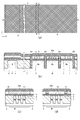
- (A) is a top view of the semiconductor device 1 manufactured by the manufacturing method of the semiconductor device by preferable embodiment of this invention.
- (B), (c), and (d) are cross-sectional views of the semiconductor device 1 corresponding to lines AA, BB, and CC, respectively, of (a).
- (A) is a top view in a manufacturing process of the semiconductor device 1 shown to Fig.1 (a).
- (B), (c), and (d) are cross-sectional views of the semiconductor device 1 corresponding to lines AA, BB, and CC, respectively, of (a).
- (A) is a top view in a manufacturing process of the semiconductor device 1 shown to Fig.1 (a).
- (B), (c), and (d) are cross-sectional views of the semiconductor device 1 corresponding to lines AA, BB, and CC, respectively, of (a).
- (A) is a top view in a manufacturing process of the semiconductor device 1 shown to Fig.1 (a).
- (B), (c), and (d) are cross-sectional views of the semiconductor device 1 corresponding to lines AA, BB, and CC, respectively, of (a).
- (A) is a top view in a manufacturing process of the semiconductor device 1 shown to Fig.1 (a).
- (B), (c), and (d) are cross-sectional views of the semiconductor device 1 corresponding to lines AA, BB, and CC, respectively, of (a).
- (A) is a top view in a manufacturing process of the semiconductor device 1 shown to Fig.1 (a).
- (B), (c), and (d) are cross-sectional views of the semiconductor device 1 corresponding to lines AA, BB, and CC, respectively, of (a).
- (A) is a top view in a manufacturing process of the semiconductor device 1 shown to Fig.1 (a).
- (B), (c), and (d) are cross-sectional views of the semiconductor device 1 corresponding to lines AA, BB, and CC, respectively, of (a).
- (A) is a top view in a manufacturing process of the semiconductor device 1 shown to Fig.1 (a).
- (B), (c), and (d) are cross-sectional views of the semiconductor device 1 corresponding to lines AA, BB, and CC, respectively, of (a).
- (A) is a top view in a manufacturing process of the semiconductor device 1 shown to Fig.1 (a).
- (B), (c), and (d) are cross-sectional views of the semiconductor device 1 corresponding to lines AA, BB, and CC, respectively, of (a).
- (A) is a top view in a manufacturing process of the semiconductor device 1 shown to Fig.1 (a).
- (B), (c), and (d) are cross-sectional views of the semiconductor device 1 corresponding to lines AA, BB, and CC, respectively, of (a).
- (A) is a top view in a manufacturing process of the semiconductor device 1 shown to Fig.1 (a).
- (B), (c), and (d) are cross-sectional views of the semiconductor device 1 corresponding to lines AA, BB, and CC, respectively, of (a).
- (A) is a top view in a manufacturing process of the semiconductor device 1 shown to Fig.1 (a).
- (B), (c), and (d) are cross-sectional views of the semiconductor device 1 corresponding to lines AA, BB, and CC, respectively, of (a).
- (A) is a top view in a manufacturing process of the semiconductor device 1 shown to Fig.1 (a).
- (B), (c), and (d) are cross-sectional views of the semiconductor device 1 corresponding to lines AA, BB, and CC, respectively, of (a).
- (A) is a top view in a manufacturing process of the semiconductor device 1 shown to Fig.1 (a).
- (B), (c), and (d) are cross-sectional views of the semiconductor device 1 corresponding to lines AA, BB, and CC, respectively, of (a).
- (A) is a top view in a manufacturing process of the semiconductor device 1 shown to Fig.1 (a).
- (B), (c), and (d) are cross-sectional views of the semiconductor device 1 corresponding to lines AA, BB, and CC, respectively, of (a).
- (A) is a top view in a manufacturing process of the semiconductor device 1 shown to Fig.1 (a).
- (B), (c), and (d) are cross-sectional views of the semiconductor device 1 corresponding to lines AA, BB, and CC, respectively, of (a).
- (A) is a top view in a manufacturing process of the semiconductor device 1 shown to Fig.1 (a).
- (B), (c), and (d) are cross-sectional views of the semiconductor device 1 corresponding to lines AA, BB, and CC, respectively, of (a).
- (A) is a top view in a manufacturing process of the semiconductor device 1 shown to Fig.1 (a).
- (B), (c), and (d) are cross-sectional views of the semiconductor device 1 corresponding to lines AA, BB, and CC, respectively, of (a).
- (A) is a top view in a manufacturing process of the semiconductor device 1 shown to Fig.1 (a).
- (B), (c), and (d) are cross-sectional views of the semiconductor device 1 corresponding to lines AA, BB, and CC, respectively, of (a).
- the semiconductor device 1 is a DRAM and has a semiconductor substrate 2 (silicon substrate) as shown in FIGS. As shown in FIG. 1A, a memory cell region M and a peripheral circuit region P are provided on the main surface of the semiconductor substrate 2.
- a rectangular active region K2 (second active region) elongated in the X direction (word line direction, first direction) shown in the figure is formed in the X direction and the Y direction (in the main surface of the semiconductor substrate 2).
- the direction intersecting with the X direction in other words, it is repeatedly arranged in each of the main surface of the semiconductor substrate 2 in the direction perpendicular to the X direction (bit line direction, second direction). That is, the plurality of active regions K2 are arranged in a matrix.
- FIG. 1A only nine active regions K2 are shown, but this is for easy understanding of the drawing and simplification of the description. Actually, a larger number of active regions K2 are arranged. .
- Each active region K2 is partitioned by an element isolation region 20 (first element isolation region) extending in the Y direction and an element isolation region 3 (second element isolation region) extending in the X direction.
- Both element isolation regions 20 and 3 are formed of an insulating film. More specifically, the element isolation region 20 is configured by a silicon nitride film, and the element isolation region 3 is configured by a silicon oxide film.
- the element isolation region 3 is also embedded in a region other than the memory cell region M as shown in FIG.
- each word line WL is arranged so as to pass through a series of active regions K2 arranged in the Y direction, and two word lines WL correspond to one active region K2.
- Two cell transistors are arranged in each active region K2, and the two word lines WL corresponding to each active region K2 each constitute a gate electrode of the cell transistor.
- Each word line WL is a buried word line composed of a conductive film buried in the main surface of the semiconductor substrate 2, and a gate insulating film 27 is disposed between each word line WL and the semiconductor substrate 2. .
- each active region K2 a region (a central portion in the X direction) located between two corresponding word lines WL is a bit line contact region BA.
- one bit line BL is provided for each series of active regions K2 arranged in the X direction.
- Each bit line BL is arranged so as to pass through each bit line contact area BA of the corresponding plurality of active regions K2. Further, each bit line BL is formed to meander as shown in FIG. 1A in order to avoid a capacitor contact plug CC described later.
- Each bit line BL and the corresponding bit line contact region BA of each active region K2 are connected to each other by a bit line contact plug BC.
- each active region K2 a region (both ends in the X direction) located outside the corresponding two word lines WL is a capacitor contact region CA.
- a cell capacitor C is disposed above each capacitor contact area CA.
- each cell capacitor C includes a lower electrode 38 for each cell capacitor C, and a capacitor insulating film 39 and an upper electrode 40 common to each cell capacitor C.
- the lower electrode 38 of each cell capacitor C is connected to the corresponding capacitor contact region CA by a capacitor contact plug CC provided therebelow.
- an impurity diffusion region 7 is provided in a portion corresponding to the capacitor contact region CA, and an impurity diffusion region 7a is provided in a portion corresponding to the bit line contact region BA.
- the impurity diffusion regions 7 and 7a constitute one and the other of the drain and the source of the corresponding cell transistor, respectively.
- the operation of the cell transistor will be described.
- a certain word line WL When a certain word line WL is activated, a channel is generated between the impurity diffusion region 7 and the impurity diffusion region 7a in the cell transistor corresponding to the word line WL. As a result, the cell transistor is turned on, and the corresponding bit line BL and the corresponding lower electrode 38 of the cell capacitor C are conducted.
- a certain word line WL becomes inactive, the channel between the impurity diffusion region 7 and the impurity diffusion region 7a disappears in the cell transistor corresponding to the word line WL. As a result, the cell transistor is turned off, and the corresponding bit line BL and the corresponding lower electrode 38 of the cell capacitor C are electrically disconnected.
- an active region KP is arranged as shown in FIG.
- FIG. 1A only one active region KP is shown, but this is for easy understanding of the drawing and simplification of the description. In reality, a larger number of active regions KP are arranged.
- the active region KP shown in FIG. 1A is a rectangle that is long in the X direction, the actual shape of the active region KP is not limited to this. In the following description, it is assumed that the active region KP is a rectangle that is long in the X direction.
- a planar transistor (peripheral circuit transistor) is formed in the active region KP shown in FIG.
- the central portion in the X direction of the active region KP is covered with the gate wiring G via the insulating film 5 (gate insulating film).
- Impurity diffusion regions 7b are formed at both ends of the active region KP in the X direction.
- the impurity diffusion region 7b corresponding to one end portion in the X direction of the active region KP is connected to the drain wiring D in the upper layer through the drain contact plug DC.
- the impurity diffusion region 7b corresponding to the other end portion in the X direction of the active region KP is connected to the source wiring S in the upper layer through the source contact plug SC.
- the drain wiring D and the source wiring S are formed in the same layer as the cell capacitor C, but the actual formation position is not limited to this.
- peripheral circuit transistors When the gate line G is activated, a channel is generated between the corresponding two impurity diffusion regions 7b. As a result, the peripheral circuit transistor is turned on, and the corresponding drain wiring D and the corresponding source wiring S are conducted. On the other hand, when the gate line G becomes inactive, the channel between the two corresponding impurity diffusion regions 7b disappears. As a result, the peripheral circuit transistor is turned off, and the corresponding drain wiring D and the corresponding source wiring S are electrically disconnected.
- FIGS. 2A to 2D by embedding an element isolation region 3 (second element isolation region) in the main surface of a semiconductor substrate 2 made of p-type silicon single crystal, A plurality of silicon pillars 4 extending in the X direction are formed in the memory cell region M, and the silicon pillars 4 are also formed in the peripheral circuit region P.
- the silicon pillars 4 in the memory cell region M constitute a plurality of active regions K1 (first active regions) extending in the X direction and repeatedly arranged in the Y direction.
- the active region K1 is divided into a plurality of the above-described active regions K2 by forming the element isolation region 20 in a later process.
- the silicon pillar 4 in the peripheral circuit region P constitutes the active region KP described above.
- the element isolation region 3 is preferably formed as follows. That is, first, a pad silicon oxide film (not shown) having a thickness of 2 nm and a silicon nitride film (not shown) having a thickness of 100 nm are sequentially formed on the main surface of the semiconductor substrate 2. Subsequently, the silicon nitride film is patterned into a pattern of the silicon pillar 4 by lithography and dry etching, and the main surface of the semiconductor substrate 2 is etched using the patterned silicon nitride film as a mask. As a result, a trench is formed in the main surface of the semiconductor substrate 2.
- a silicon oxide film (fifth insulating film) serving as a material of the element isolation region 3 is formed with a film thickness filling the inside of the trench. To do. Thereafter, the silicon oxide film and the silicon oxide film are removed by CMP (Chemical-Mechanical-Polishing) method until the main surface of the semiconductor substrate 2 is exposed. The state shown in FIGS. 2A to 2D is obtained by the above steps.
- the height D1 of the element isolation region 3 is preferably 250 nm.
- a silicon oxide film 5 is formed on the exposed surface of the semiconductor substrate 2 by using a thermal oxidation method.
- This silicon oxide film 5 is formed as a pad oxide film for protecting the semiconductor substrate 2.
- the silicon oxide film 5 formed in the active region KP is also used as a gate insulating film of the peripheral circuit transistor.
- an impurity-doped amorphous silicon film 6 having a thickness of 10 nm is formed on the entire surface, and a portion other than the peripheral circuit region P is removed. This removal is preferably performed by forming a mask pattern (not shown) that covers the peripheral circuit region P and then etching the impurity-doped amorphous silicon film 6 using this mask pattern as a mask.
- the impurity-doped amorphous silicon film 6 formed here is an insulating film, but it is modified into a conductive film during a subsequent process and becomes a part of the gate wiring G shown in FIG. .
- an impurity diffusion region 7 is formed on the active region K1 by ion implantation.
- a hard mask film 8 which is a silicon nitride film having a thickness of 40 nm is formed on the entire surface by a CVD (Chemical Vapor Deposition) method, and a spin coating method is further performed.
- the antireflection film 9a having a thickness of 200 nm and the silicon-containing antireflection film 9b having a thickness of 32 nm are sequentially formed.
- the laminated film of the antireflection film 9a and the silicon-containing antireflection film 9b constitutes a sacrificial film 9.
- the sacrificial film 9 is formed into a sacrificial film pattern (first opening) having a plurality of openings A1 (first openings) in the memory cell region M. 1 sacrificial film pattern).
- the upper surface of the hard mask film 8 is exposed on the bottom surface of each opening A1.
- Each opening A1 is disposed so as to straddle a plurality of active regions K1 (see FIG. 2A) arranged in the Y direction, and is aligned in the X direction.
- the planar shape of each opening A1 has a size in the X direction that is three times the minimum processing dimension F (3F) and a size in the Y direction that is the minimum processing dimension F.
- a rectangular shape that is 9 times (9F) is preferable.
- the size in the Y direction is determined so that the end in the Y direction of the opening A1 is located at a position 2F from the active region K1 at the extreme end in the Y direction, depending on the number of the active regions K1. Change.
- interval of the X direction of each opening A1 shall be 3 times (3F) of the minimum process dimension F, as shown to Fig.4 (a).
- a sacrificial film 11 made of a silicon oxide film (third insulating film) is formed on the entire surface.
- the film thickness of the sacrificial film 11 at this time is such that the lateral film thickness of the portion serving as the sidewall insulating film covering the inner wall of the opening A1 is the minimum processing dimension. Set to be equal to F.
- the sacrificial film 9 made of an organic antireflection film has poor heat resistance
- the sacrificial film 11 is formed by an MLD (Molecule Layer Deposition) method that can be formed at a low temperature of 100 ° C. or less. Use.
- aminosilane which is a silicon raw material
- the third step of oxidizing the adsorbed aminosilane and the fourth step of exhausting the introduced oxidant by repeating the introduction of the oxidant are repeated while maintaining the temperature of the semiconductor substrate 2 at, for example, 50 ° C. It is preferable to carry out by executing.
- the sacrificial film 11 thus formed is a laminated film in which molecular-level thin films are laminated. Note that the MLD method has the merit that the step coverage is excellent because the surface adsorption reaction is used in addition to the merit that the sacrificial film 9 can be prevented from being damaged because it can be formed at a low temperature.
- the sacrificial film 11 is etched back by anisotropic etch back using fluorine-containing plasma, so that the sacrificial film 11 is covered with a side wall insulating film (first side wall) covering the side surface (inner surface) of the opening A1. Insulating film).
- This etch back is performed until the sacrificial film 9 or the hard mask film 8 is exposed.
- the sacrificial film 9 is selectively removed by dry etching using oxygen-containing plasma. As a result, a plurality of closed loop patterns each made of the sacrificial film 11 are formed in the memory cell region M, as shown in FIG.
- the closed loop pattern (sacrificial film 11) thus formed has a shape along the inner periphery of the opening A1 shown in FIG.
- the width in the horizontal direction of each closed loop pattern (sacrificial film 11) is the minimum processing dimension F as shown in FIGS. 6 (a), 6 (b), and 6 (d). Further, the width (X-direction width) of the opening A2 formed at the center of each closed loop pattern (sacrificial film 11) is equal to the minimum processing dimension F.
- a sacrificial film 15 made of a silicon nitride film (fourth insulating film) is formed on the entire surface.
- the film thickness of the sacrificial film 15 at this time is the film thickness in the lateral direction of the portion that becomes the sidewall insulating film covering the outer peripheral wall of the closed loop pattern (sacrificial film 11). Is set equal to the minimum processing dimension F.
- the opening A2 is filled with the sacrificial film 15.
- the sacrificial film 15 is a portion (island pattern 15i) raised in an island shape at a position corresponding to each of the plurality of openings A1 shown in FIG. )have. More specifically, each island pattern 15i has a shape in which the corresponding opening A1 is expanded in the lateral four directions by the minimum processing dimension F in plan view. In the region between the island patterns 15i, a recess A3 having a width in the X direction equal to the minimum processing dimension F is formed. Further, in the following description, an area from each of the two island patterns 15i located at both ends in the X direction to a position separated by the minimum processing dimension F in the X direction is an area A4 as shown in FIG. 7B. Called.
- a photoresist 18 is applied to the entire surface. Then, by removing a part of the photoresist 18 by lithography, as shown in FIGS. 7A to 7D, the island patterns 15i, the recesses A3, and the regions A4 are exposed.
- the sacrificial film 15 is etched back by anisotropic etch back using the photoresist 18 (first mask pattern) as a mask.
- the sacrificial film 15 is etched back using a gas plasma containing trifluoromethane (CHF 3 ) gas or difluoromethane (CH 2 F 2 ) under the conditions of pressure 7 Pa, high frequency power 500 W, and bias power 100 W. Is preferably performed. If the hard mask film 8 is exposed as a result of this etch back, then the etching is continued until the upper surface of the silicon pillar 4 is exposed after changing to a condition where the silicon nitride film and the silicon oxide film are etched at a constant speed. .
- CHF 3 trifluoromethane
- CH 2 F 2 difluoromethane
- the sacrificial film 15 is processed into the shape of a sidewall insulating film (second sidewall insulating film) that covers the side surface of the sacrificial film 11.
- each island pattern 16 includes a hard mask film 8 and sacrificial films 11 and 15 formed on the upper surface of the hard mask film 8. Between the two adjacent island patterns 16 and between the island pattern 16 located at both ends in the X direction and the photoresist 18, the width in the X direction is equal to the minimum processing dimension F, and the width in the Y direction is the island pattern. An opening A5 (second opening) equal to that of 16 is formed. The island pattern 16 and the opening A5 constitute a second sacrificial film pattern.
- the opening A5 is formed in a self-alignment with the opening A1. Therefore, in this manufacturing method, the formation position of the opening A5 can be accurately matched to the formation position of the opening A5.
- the photoresist 18 is then removed. As a result, the sacrificial film 15 is exposed in the region where the photoresist 18 has been formed. Subsequently, the silicon pillar 4 is selectively etched by anisotropic dry etching using the second sacrificial film pattern (sacrificial films 11 and 15 and the hard mask film 8) as a mask. Specifically, a silicon pillar using a mixed gas plasma of hydrogen bromide (HBr), chlorine (Cl 2 ), and oxygen (O 2 ) under the conditions of pressure 0.5 Pa, high frequency power 500 W, and bias power 150 W. It is preferable to perform etching 4.
- HBr hydrogen bromide
- Cl 2 chlorine
- O 2 oxygen
- the first trench T1 is formed vertically below the opening A5.
- the depth D2 of the first trench T1 from the surface of the semiconductor substrate 2 is preferably set to 250 nm, which is the same as the height D1 of the element isolation region 3.
- the plurality of first trenches T1 thus formed extend in the Y direction, and divide the silicon pillar 4 (active region K1) in the memory cell region M in the X direction.
- each 1st trench T1 is located in the center of the X direction between adjacent opening part A1 (FIG. 4) except the thing located in both ends.
- Each portion of the divided silicon pillar 4 becomes a silicon pillar 4a, and constitutes an active region K2 shown in FIGS. 1 (a) to 1 (d).
- a silicon nitride film 20a (first insulating film) is formed on the entire surface by CVD as shown in FIGS. 10 (a) to 10 (d).
- the film thickness of the silicon nitride film 20a to be formed is set to a thickness greater than or equal to the degree of filling the first trench T1.
- the upper surfaces of the sacrificial films 11 and 15 are exposed as shown in FIGS. Thereby, an element isolation region 20 (see FIG. 1) extending in the Y direction is formed.
- the sacrificial film 11 which is a silicon oxide film is selectively removed by etching using the silicon nitride film as a mask.
- This etching is preferably performed using a hydrofluoric acid (HF) -containing solution.
- HF hydrofluoric acid
- a mask pattern 23 (second mask pattern) covering a portion extending in the X direction (both end portions in the Y direction) of each of the plurality of closed loop opening patterns A6. ) Is formed by lithography.
- the mask pattern 23 is formed so as to cover regions other than the memory cell region M.
- the silicon nitride film and the silicon oxide film are removed by anisotropic dry etching using the mask pattern 23 as a mask until the upper surface of the silicon pillar 4a is exposed.
- an opening A8 (third opening) is formed in a portion of each of the plurality of closed loop opening patterns A6 that is not covered with the mask pattern 23.
- the silicon pillar 4a and the element isolation region 3 are exposed on the bottom surface of the opening A8.
- a portion of the sacrificial film 15 formed in the opening portion (opening portion A7 shown in the drawing) of the mask pattern 23 disappears, and the hard mask film 8 is exposed in a region where the disappeared sacrificial film 15 is formed.
- the opening A8 is also formed in self-alignment with the opening A1. Therefore, in this manufacturing method, the formation position of the opening A8 can be accurately matched to the formation position of the opening A5.
- the mask pattern 23 is removed.
- the bottom surface of the opening A8 is etched by anisotropic dry etching using the silicon nitride film as a mask.
- the etching here is performed in two stages. Specifically, first, the element isolation region 3 made of a silicon oxide film is selectively etched, and then the silicon pillar 4a made of silicon is selectively etched. Thereby, as shown in FIGS. 16A to 16D, the second trench T2 is formed vertically below the opening A8.
- the second trench T2 thus formed becomes a trench extending in the Y direction at a position inscribed in two surfaces facing each other in the X direction of the opening A1 shown in FIG.
- each of the plurality of silicon pillars 4a is divided into three silicon pillars 4b.
- a gate insulating film 27 (second insulating film) covering the inner surface of the second trench T2 is formed by a thermal oxidation method, and the second A word line WL is formed by embedding the conductive film 28 in the trench T2.
- a specific method for forming the conductive film 28 it is preferable to use a method in which a metal film containing tungsten is deposited on the entire surface by a CVD method and then etched back. The etch back amount at this time is preferably adjusted so that the upper surface of the word line WL is approximately the same as the lower surface of the impurity diffusion region 7.
- a silicon nitride film is formed with a film thickness that fills the remaining portion of the second trench T2.
- This silicon nitride film is integrated with the silicon nitride film constituting the sacrificial film 15, the hard mask film 8, and the element isolation region 20, respectively.
- the silicon nitride film thus integrated is etched back to the extent that the surface of the silicon oxide film 5 is exposed.
- a cap insulating film 29 having an upper surface at the same height as the upper surface of the silicon oxide film 5 is formed above the second trench T2.
- the impurity-doped amorphous silicon film 6 exposed as a result of the etch-back of the silicon nitride film is a polycrystalline silicon film that is a conductor by the above steps. 6a.
- the polycrystalline silicon film 6a is drawn from the steps shown in FIGS. 17 (a) and 17 (b), but the actual impurity-doped amorphous silicon film 6 is subjected to several heat treatments performed in the processes so far. Through the process, it is gradually converted into the polycrystalline silicon film 6a.
- a silicon oxide film is formed on the entire surface, and etching is performed by CMP until the upper surface of the polycrystalline silicon film 6a is exposed.
- the interlayer insulating film 30 covering the region other than the peripheral circuit region P is formed.
- bit line contact holes BH shown in FIGS. 18A, 18B, and 18D are formed in the interlayer insulating film 30 by selectively etching the silicon oxide film.
- the planar position of these bit line contact holes BH is a position overlapping with the bit line contact area BA (the central portion in the X direction of the active region K2) shown in FIG. Therefore, the upper surface of the silicon pillar 4b corresponding to the bit line contact region BA is exposed at the bottom surface of each bit line contact hole BH.
- N-type impurities such as arsenic are ion-implanted into the bottom surface.
- the implanted portion of the impurity diffusion region 7 is changed to a high concentration impurity diffusion region 7a.
- a metal film 31 containing tungsten and a cover insulating film 32 made of a silicon nitride film are sequentially formed and patterned by photolithography and dry etching as shown in FIGS. In this patterning, the polycrystalline silicon film 6a in the peripheral circuit region P is also patterned at the same time.
- the patterned metal film 31 constitutes a bit line BL in the memory cell region M and a gate wiring G together with the polycrystalline silicon film 6a in the peripheral circuit region P.
- a sidewall insulating film 33 that covers the side wall of the pattern is formed.
- N-type impurities such as arsenic are ion-implanted into the upper surface of the silicon pillar 4 through the exposed silicon oxide film 5.
- impurity diffusion regions 7b are formed on both sides of the gate wiring G in the X direction when seen in a plan view.
- a silicon oxide film is formed on the entire surface, and etching is performed by CMP until the upper surface of the cover insulating film 32 is exposed.
- an interlayer insulating film 35 filling the space between the bit line BL and the gate line G is formed.
- the interlayer insulating films 35 and 30 are penetrated at a position overlapping the capacitive contact region CA (both ends in the X direction of the active region K2) shown in FIG.
- a capacitor contact plug CC is formed, and in the peripheral circuit region P, a drain contact plug DC and a source contact plug SC penetrating the interlayer insulating films 35 and 30 are formed at positions overlapping the impurity diffusion region 7b in plan view. . Further, by forming a cell capacitor C (memory cell region M), drain wiring D and source wiring S (peripheral circuit region P), interlayer insulating films 37 and 41, etc. on the upper surface of the interlayer insulating film 35, the semiconductor device 1 is formed. Is completed.
- the areas AR1 to AR3 shown in FIG. 18B are areas defined by the relationship with the opening A1 shown in FIG.
- the region AR2 (second region) is a region in the main surface of the semiconductor substrate 2 that overlaps the opening A1 when viewed in a plan view.
- the region AR1 (first region) is a region in the main surface of the semiconductor substrate 2 located between the openings A1 adjacent to each other in the X direction when seen in a plan view.
- the region AR3 is a region in the main surface of the semiconductor substrate 2 located between the region AR2 located at the extreme end in the X direction and the element isolation region 3.
- a first trench T1 having a width in the X direction of F is formed in the center of the region AR1 in the X direction. Both ends of the region AR1 in the X direction (two regions positioned between the first trench T1 and the region AR2 in plan view) are the capacitor contact regions CA, and the width of the capacitor contact region CA in the X direction is F. is there. Therefore, the width in the X direction of the region AR1 is a value 3F obtained by summing the width F in the X direction of the first trench T1 and 2F which is twice the width F in the X direction of the capacitor contact region CA. .
- the region AR2 is constituted by two second trenches T2 and a bit line contact region BA located between the two second trenches T2.
- the width in the X direction of each second trench T2 and bit line contact area BA is F. Therefore, the width of the region AR2 in the X direction is 2F, which is twice the width F of the second trench T2 in the X direction, and the value 3F obtained by adding up the width F of the bit line contact region BA in the X direction.
- the width of the region AR2 in the X direction may be less than 3F. In this case, the width of the bit line contact region BA in the X direction is less than F while maintaining the width F of the second trench T2 in the X direction. It is preferable to do.
- the region AR3 is configured by a first trench T1 adjacent to the element isolation region 3 and a capacitor contact region CA positioned between the first trench T1 and the region AR2 adjacent to the first trench T1.
- the widths in the X direction of the first trench T1 and the capacitor contact region CA are both F. Therefore, the width in the X direction of the region AR3 is a value 2F obtained by summing the width F in the X direction of the first trench T1 and the width F in the X direction of the bit line contact region BA.
- the formation position of the second trench T2 in the region AR2 is determined by the formation position of the sacrificial film 11 shown in FIG. Since the sacrificial film 11 is formed as a sidewall insulating film on the side surface of the opening A1 shown in FIG. 4B or the like, the formation position of the second trench T2 is the position of the opening A1. It can be said that it depends on.
- the formation position of the first trench T2 in the area AR1 is determined by the formation position of the island pattern 16 shown in FIG. Since this island pattern 16 is composed of the sacrificial film 11 and the sacrificial film 15 formed as a sidewall insulating film on the side surface thereof, the formation position of the first trench T1 is also the position of the opening A1.
- the element isolation region 20 embedded in the first trench T1 and the word line WL embedded in the second trench T2 satisfy the above-described definition of self-alignment and are formed in self-alignment with each other.
- the element isolation region 20 is formed of the insulating film while the word line WL and the element isolation region 20 are formed in self alignment with respect to the X direction. It becomes possible. Therefore, it is not necessary to apply a voltage to the element isolation region 20, so that the circuit can be simplified.
- both ends of the active region K2 in the X direction since the distance between the word line WL and the element isolation region 20 can be set to a constant value (the word line WL and the element isolation region 20 can be formed so as not to be shifted from each other), both ends of the active region K2 in the X direction. It is also possible to make the width in the X direction of the two capacitor contact areas CA located at a constant value. That is, when only one of the two capacitor contact regions CA is wide and the other is narrow, the contact resistance between the capacitor contact plug CC and the impurity diffusion region 7 increases in the narrower capacitor contact region CA. It will be. According to the method for manufacturing a semiconductor device according to the present embodiment, it is possible to prevent such an increase in contact resistance.
Landscapes
- Engineering & Computer Science (AREA)
- Manufacturing & Machinery (AREA)
- Semiconductor Memories (AREA)
- Physics & Mathematics (AREA)
- Condensed Matter Physics & Semiconductors (AREA)
- General Physics & Mathematics (AREA)
- Computer Hardware Design (AREA)
- Microelectronics & Electronic Packaging (AREA)
- Power Engineering (AREA)
Abstract
Description
本発明は、半導体装置の製造方法に関し、特に半導体基板に埋め込んで形成されるワード線と、ワード線方向に延在する素子分離領域とを互いに自己整合で形成する半導体装置の製造方法に関する。 The present invention relates to a method for manufacturing a semiconductor device, and more particularly to a method for manufacturing a semiconductor device in which a word line embedded in a semiconductor substrate and an element isolation region extending in the word line direction are formed in self alignment.
DRAM(Dynamic Random Access Memory)などの半導体装置では、STI(shallow trench isolation)法によってシリコン基板の表面に素子分離領域が設けられ、これによって、複数の活性領域がマトリクス状に区画される。素子分離領域には、各活性領域をビット線方向に分離する第1の素子分離領域と、ワード線方向に分離する第2の素子分離領域とが含まれる。特許文献1には、このような素子分離領域及び活性領域の例が開示されている。
In a semiconductor device such as a DRAM (Dynamic Random Access Memory), an element isolation region is provided on the surface of a silicon substrate by an STI (shallow trench isolation) method, whereby a plurality of active regions are partitioned in a matrix. The element isolation region includes a first element isolation region that isolates each active region in the bit line direction and a second element isolation region that isolates each active region in the word line direction.
ところで、特許文献1に記載の半導体装置では、ワード線が半導体基板に埋め込んだ導電膜によって構成され、このワード線(埋込ワード線)と第1の素子分離領域(ワード線方向に延在する素子分離領域)とが互いに自己整合で形成されている。以下、この点について、詳しく説明する。なお、以下の説明では、特許文献1に倣い、ワード線及び第1の素子分離領域のビット線方向の幅をそれぞれW1,W3とする。また、第1の素子分離領域と、該第1の素子分離領域に最も近いワード線との間のビット線方向の距離をW2とする。さらに、同じ活性領域内を通過する2本のワード線の間の距離をW4とする。
By the way, in the semiconductor device described in
特許文献1に記載の方法では、まず初めに半導体基板の主面を、それぞれワード線方向に延在する複数の直線状のマスクパターンで覆う。この直線状マスクパターンはビット線方向の幅が2W2+W3であるものとし、かつ隣接するマスクパターン間の距離を2W1+W4に設定する。次に、直線状マスクパターンの側壁に、ビット線方向の厚みがW1である第1のサイドウォール絶縁膜を形成し、その後直線状マスクパターンを除去する。こうして形成された第1のサイドウォール絶縁膜は、ワード線を埋め込む領域のみを覆う絶縁膜パターンとなる。続いて、第1のサイドウォール絶縁膜の側壁に、ビット線方向の厚みがW2である第2のサイドウォール絶縁膜を形成し、その後第1のサイドウォール絶縁膜を除去する。こうして形成された第2のサイドウォール絶縁膜は、素子分離領域を埋め込む領域と、ワード線を埋め込む領域とを露出させる開口を有する絶縁膜パターンとなる。したがって、第2のサイドウォール絶縁膜をマスクとして半導体基板の主面をエッチングすることにより、素子分離領域及びワード線をそれぞれ埋め込むためのトレンチを形成することが可能になる。そして、形成したトレンチの内表面を薄い絶縁膜で覆い、さらにトレンチ内に導電膜を埋め込むことにより、ワード線及び第1の素子分離領域が形成される。
In the method described in
以上説明した形成方法によれば、ワード線及び第1の素子分離領域それぞれのビット線方向の位置がいずれも、初めに形成した直線状マスクパターンの形成位置に応じて正確に規定される。本明細書では、この例のように、2種類の埋め込み膜の相対的な位置が共通のパターンの形成位置に応じて決定される場合、これら2種類の埋め込み膜が互いに自己整合で形成されているという。 According to the formation method described above, the positions of the word line and the first element isolation region in the bit line direction are both accurately defined according to the formation position of the linear mask pattern formed first. In this specification, as in this example, when the relative positions of the two types of buried films are determined according to the formation position of the common pattern, these two types of buried films are formed in a self-aligned manner. It is said.
しかしながら、特許文献1に記載の方法によれば、ワード線だけでなく第1の素子分離領域も導電膜によって構成されることになる。こうして形成される第1の素子分離領域は、いわゆる電界シールド方式によるものであり、素子分離機能を発揮させるために一定電圧を常時印加し続ける必要がある。したがって、この電圧印加のための制御用回路が必要となり、回路の複雑化を招来していた。
However, according to the method described in
本発明の一側面による半導体装置の製造方法は、半導体基板の主面に、該主面内の第1の方向に延在し、かつ該第1の方向に交差する第2の方向に繰り返し配置される複数の第1の活性領域を形成する工程と、それぞれ前記第2の方向に延在し、前記複数の第1の活性領域のそれぞれを前記第1の方向に分割してなる複数の第2の活性領域を区画する複数の第1のトレンチを形成する工程と、前記複数の第1のトレンチに第1の絶縁膜を埋め込むことにより、第1の素子分離領域を形成する工程と、前記第1の素子分離領域を形成した後、それぞれ前記第2の方向に延在する第2のトレンチを形成する工程と、前記第2のトレンチの内表面を覆う第2の絶縁膜を形成し、さらに前記第2のトレンチに導電膜を埋め込むことにより配線を形成する工程とを備え、前記第1及び第2のトレンチは、前記第1の方向に関して、互いに自己整合で形成されることを特徴とする。 According to one aspect of the present invention, there is provided a method for manufacturing a semiconductor device, wherein a semiconductor substrate is repeatedly disposed in a second direction extending in a first direction in the main surface and intersecting the first direction on the main surface of the semiconductor substrate. Forming a plurality of first active regions, and extending a plurality of first active regions each extending in the second direction and dividing each of the plurality of first active regions in the first direction. Forming a plurality of first trenches that partition two active regions, forming a first element isolation region by embedding a first insulating film in the plurality of first trenches, Forming a second trench extending in the second direction after forming the first element isolation region, and forming a second insulating film covering the inner surface of the second trench, Further, a wiring is formed by embedding a conductive film in the second trench. A that step, the first and second trenches, with respect to said first direction, characterized in that it is formed in self-alignment with each other.
本発明の他の一側面による半導体装置の製造方法は、半導体基板の主面に、該主面内の第2の方向に延在する直線状の第1の開口部を有する第1の犠牲膜パターンを形成する工程と、前記第1の開口部の内壁を覆う第1のサイドウォール絶縁膜を形成する工程と、前記第1のサイドウォール絶縁膜を形成した後、前記第1の犠牲膜パターンを除去する工程と、前記第1のサイドウォール絶縁膜の側壁を覆う第2のサイドウォール絶縁膜を形成する工程と、前記第1及び第2のサイドウォール絶縁膜をマスクとして前記主面をエッチングすることにより、第1のトレンチを形成する工程と、前記第1のトレンチに第1の絶縁膜を埋め込むことにより、第1の素子分離領域を形成する工程と、前記第1の素子分離領域を形成した後、前記第1のサイドウォール絶縁膜を除去する工程と、前記主面のうち前記第1のサイドウォール絶縁膜が形成されていた領域をエッチングすることにより、第2のトレンチを形成する工程と、前記第2のトレンチの内表面を覆う第2の絶縁膜を形成し、さらに前記第2のトレンチに導電膜を埋め込むことにより、ワード線を形成する工程とを備えることを特徴とする。 A method of manufacturing a semiconductor device according to another aspect of the present invention includes a first sacrificial film having a linear first opening extending in a second direction in a main surface of a semiconductor substrate. Forming a pattern; forming a first sidewall insulating film covering an inner wall of the first opening; and forming the first sidewall insulating film, and then forming the first sacrificial film pattern Removing the substrate, forming a second sidewall insulating film covering the sidewall of the first sidewall insulating film, and etching the main surface using the first and second sidewall insulating films as a mask. A step of forming a first trench, a step of forming a first element isolation region by embedding a first insulating film in the first trench, and a step of forming the first element isolation region. After forming, the first Removing a sidewall insulating film, forming a second trench by etching a region of the main surface where the first sidewall insulating film is formed, and the second trench. Forming a word line by forming a second insulating film covering the inner surface of the first insulating film and further burying a conductive film in the second trench.
本発明によれば、配線(ワード線)及び第1の素子分離領域を第1の方向に関して互いに自己整合で形成しつつ、第1の素子分離領域を絶縁膜によって構成することが可能になる。したがって、第1の素子分離領域に電圧を印加する必要がなくなるので、回路を簡素化することが可能になる。 According to the present invention, it is possible to configure the first element isolation region with the insulating film while forming the wiring (word line) and the first element isolation region in a self-aligned manner with respect to the first direction. Therefore, it is not necessary to apply a voltage to the first element isolation region, so that the circuit can be simplified.
以下、添付図面を参照しながら、本発明の好ましい実施の形態について詳細に説明する。以下では、まず初めに本実施の形態による半導体装置の製造方法によって製造される半導体装置1の構造の概要について説明し、続いて、半導体装置1の製造方法について詳しく説明する。
Hereinafter, preferred embodiments of the present invention will be described in detail with reference to the accompanying drawings. In the following, the outline of the structure of the
まず、図1(a)~(d)を参照しながら、半導体装置1の構造について説明する。半導体装置1はDRAMであり、図1(b)~(d)に示すように半導体基板2(シリコン基板)を有している。半導体基板2の主面には、図1(a)に示すように、メモリセル領域Mと周辺回路領域Pとが設けられる。
First, the structure of the
メモリセル領域Mには、図示したX方向(ワード線方向。第1の方向)に細長い長方形の活性領域K2(第2の活性領域)が、X方向及びY方向(半導体基板2の主面内でX方向と交差する方向。別の言い方をすれば、半導体基板2の主面内でX方向と垂直な方向。ビット線方向。第2の方向)のそれぞれに繰り返し配置される。つまり、複数の活性領域K2がマトリクス状に配置される。なお、図1(a)では9個の活性領域K2のみを示しているが、これは図面を見易くして説明を簡単にするためであり、実際にはより多数の活性領域K2が配置される。
In the memory cell region M, a rectangular active region K2 (second active region) elongated in the X direction (word line direction, first direction) shown in the figure is formed in the X direction and the Y direction (in the main surface of the semiconductor substrate 2). In the direction intersecting with the X direction, in other words, it is repeatedly arranged in each of the main surface of the
各活性領域K2は、Y方向に延在する素子分離領域20(第1の素子分離領域)と、X方向に延在する素子分離領域3(第2の素子分離領域)とによって区画される。素子分離領域20,3はともに絶縁膜によって構成される。より具体的には、素子分離領域20はシリコン窒化膜によって構成され、素子分離領域3はシリコン酸化膜によって構成される。素子分離領域3は、図1(a)等に示すように、メモリセル領域M以外の領域にも埋め込まれている。
Each active region K2 is partitioned by an element isolation region 20 (first element isolation region) extending in the Y direction and an element isolation region 3 (second element isolation region) extending in the X direction. Both
メモリセル領域Mには、それぞれX方向に延在する複数のワード線WLと、それぞれY方向に延在する複数のビット線BLとが配置される。各ワード線WLはY方向に並ぶ一連の活性領域K2を通過するように配置され、1つの活性領域K2に2本のワード線WLが対応している。各活性領域K2には2つずつセルトランジスタが配置され、各活性領域K2に対応する2本のワード線WLはそれぞれ、セルトランジスタのゲート電極を構成する。各ワード線WLは、半導体基板2の主面に埋め込まれた導電膜によって構成される埋込ワード線であり、各ワード線WLと半導体基板2との間にはゲート絶縁膜27が配置される。
In the memory cell region M, a plurality of word lines WL each extending in the X direction and a plurality of bit lines BL each extending in the Y direction are arranged. Each word line WL is arranged so as to pass through a series of active regions K2 arranged in the Y direction, and two word lines WL correspond to one active region K2. Two cell transistors are arranged in each active region K2, and the two word lines WL corresponding to each active region K2 each constitute a gate electrode of the cell transistor. Each word line WL is a buried word line composed of a conductive film buried in the main surface of the
各活性領域K2のうち、対応する2本のワード線WLの間に位置する領域(X方向の中央部分)は、ビット線コンタクト領域BAである。半導体装置1では、X方向に並ぶ一連の活性領域K2ごとに1本のビット線BLが設けられる。各ビット線BLは、対応する複数の活性領域K2それぞれのビット線コンタクト領域BAを通過するように配置される。また、各ビット線BLは、後述する容量コンタクトプラグCCを避けるため、図1(a)に示すように蛇行して形成される。各ビット線BLと対応する各活性領域K2のビット線コンタクト領域BAとは、ビット線コンタクトプラグBCによって互いに接続される。
Of each active region K2, a region (a central portion in the X direction) located between two corresponding word lines WL is a bit line contact region BA. In the
各活性領域K2のうち、対応する2本のワード線WLの外側に位置する領域(X方向の両端)は、容量コンタクト領域CAである。半導体装置1では、各容量コンタクト領域CAごとに、その上方にセルキャパシタCが配置される。各セルキャパシタCは、図1(b)に示すように、セルキャパシタCごとの下部電極38と、各セルキャパシタCに共通の容量絶縁膜39及び上部電極40とによって構成される。各セルキャパシタCの下部電極38は、その下方に設けられる容量コンタクトプラグCCによって、対応する容量コンタクト領域CAと接続される。
Of each active region K2, a region (both ends in the X direction) located outside the corresponding two word lines WL is a capacitor contact region CA. In the
半導体基板2の主面のうち、容量コンタクト領域CAに相当する部分には不純物拡散領域7が、ビット線コンタクト領域BAに相当する部分には不純物拡散領域7aが、それぞれ設けられる。不純物拡散領域7,7aはそれぞれ、対応するセルトランジスタのドレイン及びソースの一方及び他方を構成する。
Of the main surface of the
セルトランジスタの動作について説明する。あるワード線WLが活性化されると、そのワード線WLに対応するセルトランジスタでは、不純物拡散領域7と不純物拡散領域7aとの間にチャネルが発生する。これにより、セルトランジスタがオン状態となり、対応するビット線BLと対応するセルキャパシタCの下部電極38とが導通する。一方、あるワード線WLが非活性になると、そのワード線WLに対応するセルトランジスタでは、不純物拡散領域7と不純物拡散領域7aとの間のチャネルが消滅する。これにより、セルトランジスタがオフ状態となり、対応するビット線BLと対応するセルキャパシタCの下部電極38とが電気的に切り離される。
The operation of the cell transistor will be described. When a certain word line WL is activated, a channel is generated between the
周辺回路領域Pには、図1(a)に示すように、活性領域KPが配置される。なお、図1(a)では1つの活性領域KPのみを示しているが、これは図面を見易くして説明を簡単にするためであり、実際にはより多数の活性領域KPが配置される。また、図1(a)に示す活性領域KPはX方向に長い長方形であるが、実際の活性領域KPの形状がこれに限られるものではない。以下では、活性領域KPがX方向に長い長方形であることを前提として説明する。 In the peripheral circuit region P, an active region KP is arranged as shown in FIG. In FIG. 1A, only one active region KP is shown, but this is for easy understanding of the drawing and simplification of the description. In reality, a larger number of active regions KP are arranged. Moreover, although the active region KP shown in FIG. 1A is a rectangle that is long in the X direction, the actual shape of the active region KP is not limited to this. In the following description, it is assumed that the active region KP is a rectangle that is long in the X direction.
図1(a)に示す活性領域KP内には、1つのプレーナ型トランジスタ(周辺回路トランジスタ)が形成される。活性領域KPのX方向の中央部は、絶縁膜5(ゲート絶縁膜)を介してゲート配線Gに覆われている。また、活性領域KPのX方向の両端部にはそれぞれ不純物拡散領域7bが形成される。このうち、活性領域KPのX方向の一方端部に対応する不純物拡散領域7bは、ドレインコンタクトプラグDCを介して、上層のドレイン配線Dに接続される。一方、活性領域KPのX方向の他方端部に対応する不純物拡散領域7bは、ソースコンタクトプラグSCを介して、上層のソース配線Sに接続される。なお、図1(b)では、ドレイン配線D及びソース配線SがセルキャパシタCと同じ層に形成されているが、実際の形成位置はこれに限られない。
1 A planar transistor (peripheral circuit transistor) is formed in the active region KP shown in FIG. The central portion in the X direction of the active region KP is covered with the gate wiring G via the insulating film 5 (gate insulating film).
周辺回路トランジスタの動作について説明する。ゲート配線Gが活性化されると、対応する2つの不純物拡散領域7b間にチャネルが発生する。これにより、周辺回路トランジスタはオン状態となり、対応するドレイン配線Dと対応するソース配線Sとが導通する。一方、ゲート配線Gが非活性になると、対応する2つの不純物拡散領域7b間のチャネルが消滅する。これにより、周辺回路トランジスタはオフ状態となり、対応するドレイン配線Dと対応するソース配線Sとが電気的に切り離される。
The operation of peripheral circuit transistors will be described. When the gate line G is activated, a channel is generated between the corresponding two
以上が、半導体装置1の構造の概要である。次に、図2~図19を参照しながら、半導体装置1の製造方法について詳しく説明する。
The above is the outline of the structure of the
初めに、図2(a)~(d)に示すように、p型のシリコン単結晶からなる半導体基板2の主面に素子分離領域3(第2の素子分離領域)を埋め込むことにより、それぞれX方向に延在する複数のシリコンピラー4をメモリセル領域M内に形成するとともに、周辺回路領域P内にもシリコンピラー4を形成する。メモリセル領域M内のシリコンピラー4は、X方向に延在し、かつY方向に繰り返し配置される複数の活性領域K1(第1の活性領域)を構成する。活性領域K1は、後の工程で素子分離領域20を形成することにより、それぞれ複数の上述した活性領域K2に分割される。周辺回路領域P内のシリコンピラー4は、上述した活性領域KPを構成する。なお、メモリセル領域M内においては、シリコンピラー4(活性領域K1)のY方向の幅及びY方向の間隔を、図2(a)に示すように、リソグラフィの解像限界で規定される最小加工寸法F(=30nm)に等しい値とすることが好ましい。
First, as shown in FIGS. 2A to 2D, by embedding an element isolation region 3 (second element isolation region) in the main surface of a
素子分離領域3は、具体的には次のようにして形成することが好適である。すなわち、まず初めに、半導体基板2の主面に厚さ2nmのパッドシリコン酸化膜(不図示)と、厚さ100nmのシリコン窒化膜(不図示)とを順次成膜する。続いて、リソグラフィとドライエッチング法によって、シリコン窒化膜をシリコンピラー4のパターンにパターニングし、パターニングされたシリコン窒化膜をマスクとして半導体基板2の主面をエッチングする。これにより半導体基板2の主面にトレンチが形成されるので、次に、このトレンチの内部を埋める膜厚で、素子分離領域3の材料となるシリコン酸化膜(第5の絶縁膜)を成膜する。その後、半導体基板2の主面が露出する程度まで、CMP(Chemical Mechanical Polishing)法によって、シリコン酸化膜及びシリコン酸化膜を除去する。以上の工程により、図2(a)~(d)に示した状態が得られる。なお、素子分離領域3の高さD1は、250nmとすることが好ましい。
Specifically, the
次に、熱酸化法を用いて、図3(a)~(d)に示すように、半導体基板2の露出面にシリコン酸化膜5を形成する。このシリコン酸化膜5は、半導体基板2を保護するためのパッド酸化膜として形成されるものである。ただし、活性領域KPに形成されたシリコン酸化膜5は、周辺回路トランジスタのゲート絶縁膜としても利用される。
Next, as shown in FIGS. 3A to 3D, a
シリコン酸化膜5を形成したら、厚さ10nmの不純物ドープ非晶質シリコン膜6を全面に成膜し、そのうち周辺回路領域P以外に形成された部分を除去する。この除去は、周辺回路領域Pを覆うマスクパターン(不図示)を形成した後、このマスクパターンをマスクとして不純物ドープ非晶質シリコン膜6をエッチングすることにより行うことが好適である。ここで形成した不純物ドープ非晶質シリコン膜6は絶縁膜であるが、後の工程を経る間に導電膜に改質され、図1(b)等に示したゲート配線Gの一部となる。周辺回路領域P以外の不純物ドープ非晶質シリコン膜6を除去した後には、イオン注入法により、活性領域K1の上部に不純物拡散領域7を形成する。
After the
次に、図4(a)~(d)に示すように、CVD(Chemical Vapor Deposition)法によって厚さ40nmのシリコン窒化膜であるハードマスク膜8を全面に成膜し、さらに回転塗布法を用いて厚さ200nmの反射防止膜9a及び厚さ32nmのシリコン含有反射防止膜9bを順次成膜する。反射防止膜9a及びシリコン含有反射防止膜9bの積層膜は、犠牲膜9を構成する。その後、図示しないマスクパターンをマスクとする異方性ドライエッチングを行うことにより、犠牲膜9を、メモリセル領域M内に複数の開口部A1(第1の開口部)を有する犠牲膜パターン(第1の犠牲膜パターン)に加工する。各開口部A1の底面には、ハードマスク膜8の上面が露出する。
Next, as shown in FIGS. 4A to 4D, a
各開口部A1は、それぞれがY方向に並ぶ複数の活性領域K1(図2(a)参照)に跨るように配置され、かつX方向に整列して配置される。各開口部A1の平面的な形状は、図4(a)に示すように、X方向のサイズが最小加工寸法Fの3倍(3F)であり、かつY方向のサイズが最小加工寸法Fの9倍(9F)である矩形とすることが好ましい。なお、Y方向のサイズは、Y方向の最端にある活性領域K1から2Fの位置に開口部A1のY方向の端部が位置するように決めているものであり、活性領域K1の数によって変化する。また、各開口部A1のX方向の間隔は、図4(a)に示すように、最小加工寸法Fの3倍(3F)とすることが好ましい。 Each opening A1 is disposed so as to straddle a plurality of active regions K1 (see FIG. 2A) arranged in the Y direction, and is aligned in the X direction. As shown in FIG. 4A, the planar shape of each opening A1 has a size in the X direction that is three times the minimum processing dimension F (3F) and a size in the Y direction that is the minimum processing dimension F. A rectangular shape that is 9 times (9F) is preferable. The size in the Y direction is determined so that the end in the Y direction of the opening A1 is located at a position 2F from the active region K1 at the extreme end in the Y direction, depending on the number of the active regions K1. Change. Moreover, it is preferable that the space | interval of the X direction of each opening A1 shall be 3 times (3F) of the minimum process dimension F, as shown to Fig.4 (a).
次に、図5(a)~(d)に示すように、全面にシリコン酸化膜(第3の絶縁膜)からなる犠牲膜11を成膜する。このときの犠牲膜11の成膜量は、図5(b)(d)に示すように、開口部A1の内壁を覆うサイドウォール絶縁膜となる部分の横方向の膜厚が、最小加工寸法Fに等しくなるように設定する。また、有機物である反射防止膜で構成されている犠牲膜9が耐熱性に乏しいため、犠牲膜11の成膜には、100℃以下の低温で成膜可能なMLD(Molecule Layer Deposition)法を用いる。
Next, as shown in FIGS. 5A to 5D, a
MLD法による成膜は、シリコン原料となるアミノシランを成膜室に導入し、半導体基板2に吸着させる第1のステップと、成膜室内に残留するアミノシランを排気する第2のステップと、オゾンなどの酸化剤を導入することにより、吸着したアミノシランを酸化する第3のステップと、導入した酸化剤を排気する第4のステップとを、半導体基板2の温度を例えば50℃に保持した状態で繰り返し実行することによって行うことが好適である。こうして形成された犠牲膜11は、分子レベルの薄膜が積層されてなる積層膜となる。なお、MLD法には、低温で成膜可能であることから犠牲膜9の受けるダメージが抑えられるというメリットの他にも、表面吸着反応を利用することから段差被覆性に優れるというメリットがある。
In the film formation by the MLD method, aminosilane, which is a silicon raw material, is introduced into the film formation chamber and is adsorbed to the
次に、フッ素含有プラズマを用いる異方性エッチバックによって犠牲膜11をエッチバックすることにより、犠牲膜11を、開口部A1の側面(内表面)を覆うサイドウォール絶縁膜(第1のサイドウォール絶縁膜)の形状に加工する。このエッチバックは、犠牲膜9又はハードマスク膜8が露出する程度まで行う。続いて、酸素含有プラズマを用いるドライエッチングによって、図6(a)~(d)に示すように、犠牲膜9を選択的に除去する。これにより、メモリセル領域M内には、図6(a)に示すように、それぞれ犠牲膜11からなる複数の閉ループパターンが形成される。こうして形成された閉ループパターン(犠牲膜11)は、図4(a)に示した開口部A1の内周に沿う形状を有している。各閉ループパターン(犠牲膜11)の横方向の幅は、図6(a)(b)(d)に示すように、最小加工寸法Fとなる。また、各閉ループパターン(犠牲膜11)の中央に形成される開口部A2の幅(X方向の幅)は、最小加工寸法Fに等しい値となる。
Next, the
次に、図7(a)~(d)に示すように、全面にシリコン窒化膜(第4の絶縁膜)からなる犠牲膜15を成膜する。このときの犠牲膜15の成膜量は、図7(b)(d)に示すように、閉ループパターン(犠牲膜11)の外周壁を覆うサイドウォール絶縁膜となる部分の横方向の膜厚が、最小加工寸法Fに等しくなるように設定する。これにより、開口部A2は、犠牲膜15によって埋め込まれる。
Next, as shown in FIGS. 7A to 7D, a
犠牲膜15は、図7(a)~(d)に示すように、図4(a)等に示した複数の開口部A1それぞれに対応する位置に、島状に盛り上がった部分(島パターン15i)を有している。より詳細には、各島パターン15iは、平面的に見て、対応する開口部A1を横方向の四方に最小加工寸法Fずつ広げた形状を有している。島パターン15i間の領域には、X方向の幅が最小加工寸法Fに等しい凹部A3が形成される。また、以下の説明では、X方向の両端に位置する2つの島パターン15iのそれぞれからX方向に最小加工寸法Fだけ離れたところまでの領域を、図7(b)に示すように、領域A4と称する。
As shown in FIGS. 7A to 7D, the
犠牲膜15を成膜したら、次に、全面にフォトレジスト18を塗布する。そして、リソグラフィによってフォトレジスト18の一部を除去することにより、図7(a)~(d)に示すように、各島パターン15i、各凹部A3、及び各領域A4を露出させる。
After the
続いてフォトレジスト18(第1のマスクパターン)をマスクとする異方性エッチバックによって、犠牲膜15をエッチバックする。具体的には、圧力7Pa、高周波パワー500W、バイアスパワー100Wの条件の下、トリフロロメタン(CHF3)ガス又はジフロロメタン(CH2F2)を含有するガスプラズマを用いて犠牲膜15のエッチバックを行うことが好適である。このエッチバックの結果としてハードマスク膜8が露出したら、次に、シリコン窒化膜とシリコン酸化膜が等速でエッチングされる条件に変更したうえで、シリコンピラー4の上面が露出するまでエッチングを続ける。これにより、犠牲膜11,15それぞれの上面が、図8(a)~(d)に示すように面一の状態となる。また、犠牲膜15は、犠牲膜11の側面を覆うサイドウォール絶縁膜(第2のサイドウォール絶縁膜)の形状に加工される。
Subsequently, the
ここまでの工程により、図8(a)~(d)に示すように、半導体基板2の主面には、図4(a)等に示した開口部A1ごとの島パターン16が形成される。各島パターン16は、ハードマスク膜8と、該ハードマスク膜8の上面に形成された犠牲膜11,15によって構成される。隣接する2つの島パターン16の間、及びX方向の両端に位置する島パターン16とフォトレジスト18との間には、X方向の幅が最小加工寸法Fに等しく、Y方向の幅が島パターン16のそれと等しい開口部A5(第2の開口部)が形成される。これら島パターン16及び開口部A5により、第2の犠牲膜パターンが構成される。
Through the steps so far, as shown in FIGS. 8A to 8D, the
ここまでの説明から明らかなように、開口部A5は、開口部A1に対して自己整合で形成されている。したがって、本製造方法においては、開口部A5の形成位置を、開口部A5の形成位置に対して精度よく合わせることが可能になる。 As is clear from the above description, the opening A5 is formed in a self-alignment with the opening A1. Therefore, in this manufacturing method, the formation position of the opening A5 can be accurately matched to the formation position of the opening A5.
島パターン16の形成が完了したら、次にフォトレジスト18を除去する。その結果、フォトレジスト18が形成されていた領域には、犠牲膜15が露出することになる。続いて、第2の犠牲膜パターン(犠牲膜11,15及びハードマスク膜8)をマスクとする異方性ドライエッチングにより、シリコンピラー4を選択的にエッチングする。具体的には、圧力0.5Pa、高周波パワー500W、バイアスパワー150Wの条件の下、臭化水素(HBr)、塩素(Cl2)、及び酸素(O2)の混合ガスプラズマを用いてシリコンピラー4のエッチングを行うことが好適である。
When the formation of the
ここまでの工程により、図9(a)~(d)に示すように、開口部A5の鉛直下方に第1のトレンチT1が形成される。なお、第1のトレンチT1の半導体基板2の表面からの深さD2は、素子分離領域3の高さD1と同じ250nmに設定することが好ましい。こうして形成された複数の第1のトレンチT1は、それぞれY方向に延在し、メモリセル領域M内のシリコンピラー4(活性領域K1)をX方向に分割する。また、各第1のトレンチT1は、両端に位置するものを除き、隣接する開口部A1(図4)の間のX方向の中央に位置している。分割されたシリコンピラー4の各部分はシリコンピラー4aとなり、図1(a)~(d)に示した活性領域K2を構成する。
Through the steps so far, as shown in FIGS. 9A to 9D, the first trench T1 is formed vertically below the opening A5. The depth D2 of the first trench T1 from the surface of the
第1のトレンチT1を形成したら、次に、CVD法によって、図10(a)~(d)に示すように全面にシリコン窒化膜20a(第1の絶縁膜)を成膜する。ここで成膜するシリコン窒化膜20aの膜厚は、第1のトレンチT1を埋める程度以上の膜厚とする。そして、成膜したシリコン窒化膜20aをエッチバックすることにより、図11(a)~(d)に示すように、犠牲膜11,15の上面を露出させる。これにより、Y方向に延在する素子分離領域20(図1参照)が形成される。
After the formation of the first trench T1, a
次に、シリコン窒化膜をマスクとするエッチングにより、シリコン酸化膜である犠牲膜11を選択的に除去する。このエッチングは、フッ酸(HF)含有溶液を用いて行うことが好ましい。これにより、図12(a)~(d)に示すように、それぞれの底面にハードマスク膜8の上面が露出した複数の閉ループ開口パターンA6が形成される。
Next, the
次いで、図13(a)~(d)に示すように、複数の閉ループ開口パターンA6それぞれのうちX方向に延在する部分(Y方向の両端部分)を覆うマスクパターン23(第2のマスクパターン)を、リソグラフィにより形成する。このマスクパターン23は、メモリセル領域M以外の領域も覆うように形成される。そして、マスクパターン23をマスクとする異方性ドライエッチングにより、図14(a)~(d)に示すように、シリコンピラー4aの上面が露出するまでシリコン窒化膜及びシリコン酸化膜を除去する。このプロセスにより、複数の閉ループ開口パターンA6それぞれのうちマスクパターン23に覆われていない部分に、開口部A8(第3の開口部)が形成される。開口部A8の底面には、シリコンピラー4a及び素子分離領域3が露出する。犠牲膜15のうちマスクパターン23の開口部(図示した開口部A7)内に形成されていた部分は消滅し、消滅した犠牲膜15が形成されていた領域にはハードマスク膜8が露出する。
Next, as shown in FIGS. 13A to 13D, a mask pattern 23 (second mask pattern) covering a portion extending in the X direction (both end portions in the Y direction) of each of the plurality of closed loop opening patterns A6. ) Is formed by lithography. The
ここまでの説明から明らかなように、開口部A8も、開口部A1に対して自己整合で形成されている。したがって、本製造方法においては、開口部A8の形成位置も、開口部A5の形成位置に対して精度よく合わせることが可能になる。 As is clear from the description so far, the opening A8 is also formed in self-alignment with the opening A1. Therefore, in this manufacturing method, the formation position of the opening A8 can be accurately matched to the formation position of the opening A5.
次に、図15(a)~(d)に示すように、マスクパターン23を除去する。そして、シリコン窒化膜をマスクとする異方性ドライエッチングにより、開口部A8の底面をエッチングする。上述したように、開口部A8の底面にはシリコンピラー4a及び素子分離領域3が露出しているため、ここでのエッチングは2段階で行う。具体的には、初めにシリコン酸化膜からなる素子分離領域3を選択的にエッチングし、次にシリコンからなるシリコンピラー4aを選択的にエッチングする。これにより、図16(a)~(d)に示すように、開口部A8の鉛直下方に第2のトレンチT2が形成される。こうして形成された第2のトレンチT2は、図4(a)等に示した開口部A1それぞれのX方向に対向する2つの表面に内接する位置でY方向に延在するトレンチとなる。第2のトレンチT2を形成したことにより、複数のシリコンピラー4aはそれぞれ3つのシリコンピラー4bに分割される。
Next, as shown in FIGS. 15A to 15D, the
次に、図16(a)~(d)に示すように、第2のトレンチT2の内表面を覆うゲート絶縁膜27(第2の絶縁膜)を熱酸化法により形成し、さらに第2のトレンチT2に導電膜28を埋め込むことにより、ワード線WLを形成する。導電膜28の具体的な形成方法としては、タングステンを含むメタル膜をCVD法により全面に堆積した後、これをエッチバックするという方法を用いることが好適である。このときのエッチバック量は、ワード線WLの上面が不純物拡散領域7の下面と同程度となるように調整することが好ましい。
Next, as shown in FIGS. 16A to 16D, a gate insulating film 27 (second insulating film) covering the inner surface of the second trench T2 is formed by a thermal oxidation method, and the second A word line WL is formed by embedding the
続いて、第2のトレンチT2の残りの部分を埋める膜厚でシリコン窒化膜を成膜する。このシリコン窒化膜は、犠牲膜15、ハードマスク膜8、及び素子分離領域20をそれぞれ構成するシリコン窒化膜と一体化する。次に、こうして一体化したシリコン窒化膜を、シリコン酸化膜5の表面を露出する程度までエッチバックする。これにより、図17(a)~(d)に示すように、第2のトレンチT2の上部に、シリコン酸化膜5の上面と同じ高さに上面を有するキャップ絶縁膜29が形成される。
Subsequently, a silicon nitride film is formed with a film thickness that fills the remaining portion of the second trench T2. This silicon nitride film is integrated with the silicon nitride film constituting the
なお、図17(a)(b)に示すように、シリコン窒化膜のエッチバックの結果として露出した不純物ドープ非晶質シリコン膜6は、ここまでの工程により、導電体である多結晶シリコン膜6aに変換されている。図面上では、図17(a)(b)に示す工程から多結晶シリコン膜6aとして描いているが、実際の不純物ドープ非晶質シリコン膜6は、ここまでのプロセスで実施したいくつかの熱処理工程を通じて、徐々に多結晶シリコン膜6aに変換される。
Note that, as shown in FIGS. 17A and 17B, the impurity-doped
次に、全面にシリコン酸化膜を形成し、CMP法により多結晶シリコン膜6aの上面が露出するまでエッチングする。これにより、図18(a)~(d)に示すように、周辺回路領域P以外の領域を覆う層間絶縁膜30が形成される。
Next, a silicon oxide film is formed on the entire surface, and etching is performed by CMP until the upper surface of the
続いて、シリコン酸化膜を選択的にエッチングすることによって、図18(a)(b)(d)に示す複数のビット線コンタクトホールBHを層間絶縁膜30に形成する。これらビット線コンタクトホールBHの平面的な位置は、図1(a)にも示したビット線コンタクト領域BA(活性領域K2のX方向の中央部分)と平面的に見て重なる位置とする。したがって、各ビット線コンタクトホールBHの底面には、ビット線コンタクト領域BAに相当するシリコンピラー4bの上面が露出する。
Subsequently, a plurality of bit line contact holes BH shown in FIGS. 18A, 18B, and 18D are formed in the
ビット線コンタクトホールBHを形成したら、その底面にヒ素などのN型不純物をイオン注入する。これにより、注入した部分の不純物拡散領域7が、高濃度の不純物拡散領域7aに変化する。その後、タングステンを含む金属膜31と、シリコン窒化膜からなるカバー絶縁膜32を順次成膜し、フォトリソグラフィ及びドライエッチングにより、図19(a)~(d)に示すようにパターニングする。このパターニングでは、周辺回路領域Pの多結晶シリコン膜6aも同時にパターニングする。パターニング後の金属膜31は、メモリセル領域Mではビット線BLを、周辺回路領域Pでは多結晶シリコン膜6aとともにゲート配線Gを、それぞれ構成する。パターニングの終了後には、パターンの側壁を覆うサイドウォール絶縁膜33を形成する。また、周辺回路領域Pでは、シリコンピラー4の上面に、露出しているシリコン酸化膜5を介して、ヒ素などのN型不純物をイオン注入する。これにより、平面的に見てゲート配線GのX方向の両側に、不純物拡散領域7bが形成される。
After the bit line contact hole BH is formed, N-type impurities such as arsenic are ion-implanted into the bottom surface. Thereby, the implanted portion of the
次に、全面にシリコン酸化膜を形成し、CMP法によりカバー絶縁膜32の上面が露出するまでエッチングする。これにより、図1(a)~(d)に示すように、ビット線BL及びゲート配線Gの間の空間を充填する層間絶縁膜35が形成される。その後、メモリセル領域Mでは、図1(a)に示した容量コンタクト領域CA(活性領域K2のX方向の両端部)と平面的に見て重なる位置に、層間絶縁膜35,30を貫通する容量コンタクトプラグCCを形成し、周辺回路領域Pでは、不純物拡散領域7bと平面的に見て重なる位置に、それぞれ層間絶縁膜35,30を貫通するドレインコンタクトプラグDC及びソースコンタクトプラグSCを形成する。さらに、層間絶縁膜35の上面に、セルキャパシタC(メモリセル領域M)、ドレイン配線D及びソース配線S(周辺回路領域P)、層間絶縁膜37,41などを形成することにより、半導体装置1が完成する。
Next, a silicon oxide film is formed on the entire surface, and etching is performed by CMP until the upper surface of the
ここで、図18(b)を再度参照し、第1及び第2のトレンチT1,T2、ビット線コンタクト領域BA、容量コンタクト領域CAのX方向の位置関係について、より詳しくかつまとめて説明する。 Here, with reference to FIG. 18B again, the positional relationship in the X direction of the first and second trenches T1, T2, the bit line contact region BA, and the capacitor contact region CA will be described in more detail and collectively.
図18(b)に示した領域AR1~AR3は、図4(b)等に示した開口部A1との関係で規定される領域である。具体的に説明すると、領域AR2(第2の領域)は、平面的に見て開口部A1と重なる半導体基板2の主面内の領域である。一方、領域AR1(第1の領域)は、平面的に見てX方向に互いに隣接する開口部A1の間に位置する半導体基板2の主面内の領域である。さらに、領域AR3は、X方向の最端に位置する領域AR2と、素子分離領域3との間に位置する半導体基板2の主面内の領域である。
The areas AR1 to AR3 shown in FIG. 18B are areas defined by the relationship with the opening A1 shown in FIG. Specifically, the region AR2 (second region) is a region in the main surface of the
領域AR1のX方向の中央には、X方向の幅がFである第1のトレンチT1が形成される。領域AR1のX方向の両端(平面的に見て第1のトレンチT1と領域AR2の間に位置する2つの領域)は容量コンタクト領域CAであり、容量コンタクト領域CAのX方向の幅はFである。したがって、領域AR1のX方向の幅は、第1のトレンチT1のX方向の幅Fと、容量コンタクト領域CAのX方向の幅Fの2倍である2Fとを合計してなる値3Fとなる。
In the center of the region AR1 in the X direction, a first trench T1 having a width in the X direction of F is formed. Both ends of the region AR1 in the X direction (two regions positioned between the first trench T1 and the region AR2 in plan view) are the capacitor contact regions CA, and the width of the capacitor contact region CA in the X direction is F. is there. Therefore, the width in the X direction of the region AR1 is a
領域AR2は、2本の第2のトレンチT2と、該2本の第2のトレンチT2の間に位置するビット線コンタクト領域BAとによって構成される。各第2のトレンチT2及びビット線コンタクト領域BAのX方向の幅は、いずれもFである。したがって、領域AR2のX方向の幅は、第2のトレンチT2のX方向の幅Fの2倍である2Fと、ビット線コンタクト領域BAのX方向の幅Fとを合計してなる値3Fとなる。なお、領域AR2のX方向の幅は3F未満でもよく、その場合には、第2のトレンチT2のX方向の幅Fを維持しつつ、ビット線コンタクト領域BAのX方向の幅をF未満とすることが好ましい。
The region AR2 is constituted by two second trenches T2 and a bit line contact region BA located between the two second trenches T2. The width in the X direction of each second trench T2 and bit line contact area BA is F. Therefore, the width of the region AR2 in the X direction is 2F, which is twice the width F of the second trench T2 in the X direction, and the
領域AR3は、素子分離領域3に隣接する第1のトレンチT1と、該第1のトレンチT1と隣接する領域AR2との間に位置する容量コンタクト領域CAとによって構成される。第1のトレンチT1及び容量コンタクト領域CAのX方向の幅は、いずれもFである。したがって、領域AR3のX方向の幅は、第1のトレンチT1のX方向の幅Fと、ビット線コンタクト領域BAのX方向の幅Fとを合計してなる値2Fとなる。
The region AR3 is configured by a first trench T1 adjacent to the
領域AR2内の第2のトレンチT2の形成位置は、図6(b)等に示した犠牲膜11の形成位置によって決まる。この犠牲膜11は、図4(b)等に示した開口部A1の側面にサイドウォール絶縁膜として形成されたものであることから、第2のトレンチT2の形成位置は、開口部A1の位置によって決まると言える。また、領域AR1内の第1のトレンチT2の形成位置は、図8(b)等に示した島パターン16の形成位置によって決まる。この島パターン16は、犠牲膜11と、その側面にサイドウォール絶縁膜として形成された犠牲膜15とによって構成されるものであることから、第1のトレンチT1の形成位置も、開口部A1の位置によって決まると言える。したがって、第1のトレンチT1に埋め込まれる素子分離領域20と、第2のトレンチT2に埋め込まれるワード線WLとは、上述した自己整合の定義を満たし、互いに自己整合で形成されていると言える。
The formation position of the second trench T2 in the region AR2 is determined by the formation position of the
以上説明したように、本実施の形態による半導体装置の製造方法によれば、ワード線WL及び素子分離領域20をX方向に関して互いに自己整合で形成しつつ、素子分離領域20を絶縁膜によって構成することが可能になる。したがって、素子分離領域20に電圧を印加する必要がなくなるので、回路を簡素化することが可能になる。
As described above, according to the manufacturing method of the semiconductor device according to the present embodiment, the
また、ワード線WL及び素子分離領域20の間隔を一定値とすることができる(ワード線WLと素子分離領域20とを、互いにずれないように形成できる)ので、活性領域K2のX方向の両端に位置する2つの容量コンタクト領域CAのX方向の幅も一定値とすることが可能になる。つまり、2つの容量コンタクト領域CAのいずれか一方のみが広く、他方が狭いという状態になると、狭い方の容量コンタクト領域CAでは、容量コンタクトプラグCCと不純物拡散領域7の接触抵抗が増大してしまうことになる。本実施の形態による半導体装置の製造方法によれば、このような接触抵抗の増大を防止することが可能になる。
In addition, since the distance between the word line WL and the
以上、本発明の好ましい実施形態について説明したが、本発明は、上記の実施形態に限定されることなく、本発明の主旨を逸脱しない範囲で種々の変更が可能であり、それらも本発明の範囲内に包含されるものであることはいうまでもない。 The preferred embodiments of the present invention have been described above, but the present invention is not limited to the above-described embodiments, and various modifications can be made without departing from the spirit of the present invention. Needless to say, it is included in the range.
1 半導体装置
2 半導体基板
3 素子分離領域(第5の絶縁膜)
4,4a,4b シリコンピラー
5 絶縁膜(シリコン酸化膜)
6 不純物ドープ非晶質シリコン膜
6a 多結晶シリコン膜
7,7a,7b 不純物拡散領域
8 ハードマスク膜
9 犠牲膜(第1の犠牲膜パターン)
9a 反射防止膜
9b シリコン含有反射防止膜
11 犠牲膜(第3の絶縁膜、第1のサイドウォール絶縁膜)
15 犠牲膜(第4の絶縁膜、第2のサイドウォール絶縁膜)
15i 島パターン
16 島パターン(第2の犠牲膜パターン)
18 フォトレジスト(第1のマスクパターン)
20 素子分離領域
20a シリコン窒化膜(第1の絶縁膜)
23 マスクパターン(第2のマスクパターン)
27 ゲート絶縁膜(第2の絶縁膜)
28 導電膜
29 キャップ絶縁膜
30,35,37,41 層間絶縁膜
31 金属膜
32 カバー絶縁膜
33 サイドウォール絶縁膜
38 下部電極
39 容量絶縁膜
40 上部電極
A1 開口部(第1の開口部)
A2 開口部
A3 凹部
A4 領域
A5 開口部(第2の開口部)
A6 閉ループ開口パターン
A7 開口部
A8 開口部(第3の開口部)
AR1 第1の領域
AR2 第2の領域
AR3 領域
BA ビット線コンタクト領域
BC ビット線コンタクトプラグ
BH ビット線コンタクトホール
BL ビット線
C セルキャパシタ
CA 容量コンタクト領域
CC 容量コンタクトプラグ
D ドレイン配線
DC ドレインコンタクトプラグ
G ゲート配線
K1 第1の活性領域
K2 第2の活性領域
KP 活性領域
M メモリセル領域
P 周辺回路領域
S ソース配線
SC ソースコンタクトプラグ
T1 第1のトレンチ
T2 第2のトレンチ
WL ワード線
DESCRIPTION OF
4, 4a,
6 Impurity doped
15 Sacrificial film (fourth insulating film, second sidewall insulating film)
18 Photoresist (first mask pattern)
20
23 Mask pattern (second mask pattern)
27 Gate insulating film (second insulating film)
28
A2 Opening A3 Recess A4 Region A5 Opening (second opening)
A6 Closed loop opening pattern A7 Opening A8 Opening (third opening)
AR1 First region AR2 Second region AR3 Region BA Bit line contact region BC Bit line contact plug BH Bit line contact hole BL Bit line C Cell capacitor CA Capacitor contact region CC Capacitor contact plug D Drain wiring DC Drain contact plug G Gate Wiring K1 first active region K2 second active region KP active region M memory cell region P peripheral circuit region S source wiring SC source contact plug T1 first trench T2 second trench WL word line
Claims (17)
それぞれ前記第2の方向に延在し、前記複数の第1の活性領域のそれぞれを前記第1の方向に分割してなる複数の第2の活性領域を区画する複数の第1のトレンチを形成する工程と、
前記複数の第1のトレンチに第1の絶縁膜を埋め込むことにより、第1の素子分離領域を形成する工程と、
前記第1の素子分離領域を形成した後、それぞれ前記第2の方向に延在する第2のトレンチを形成する工程と、
前記第2のトレンチの内表面を覆う第2の絶縁膜を形成し、さらに前記第2のトレンチに導電膜を埋め込むことにより配線を形成する工程とを備え、
前記第1及び第2のトレンチは、前記第1の方向に関して、互いに自己整合で形成されることを特徴とする半導体装置の製造方法。 Forming a plurality of first active regions on a main surface of a semiconductor substrate, the first active regions extending in a first direction within the main surface and repeatedly arranged in a second direction intersecting the first direction; When,
A plurality of first trenches extending in the second direction and partitioning a plurality of second active regions formed by dividing each of the plurality of first active regions in the first direction are formed. And a process of
Forming a first element isolation region by embedding a first insulating film in the plurality of first trenches;
Forming a second trench extending in the second direction after forming the first element isolation region; and
Forming a second insulating film covering an inner surface of the second trench, and further forming a wiring by embedding a conductive film in the second trench,
The method of manufacturing a semiconductor device, wherein the first and second trenches are formed in a self-aligned manner with respect to the first direction.
前記第1のトレンチは、隣接する前記第1の開口部の間の前記第1の方向の中央に位置して前記第2の方向に延在し、
前記第2のトレンチは、前記複数の第1の開口部それぞれの前記第1の方向に対向する2つの表面に内接する位置で前記第2の方向に延在する
ことを特徴とする請求項1に記載の半導体装置の製造方法。 Forming a first sacrificial film pattern having a plurality of first openings straddling a plurality of the first active regions respectively arranged in the first direction,
The first trench is located in the center of the first direction between the adjacent first openings and extends in the second direction,
2. The second trench extends in the second direction at a position inscribed in two surfaces of the plurality of first openings facing each other in the first direction. The manufacturing method of the semiconductor device as described in any one of.
前記第1のトレンチを形成する工程では、前記第2の犠牲膜パターンをマスクとして前記第2の開口部の鉛直下方に位置する前記半導体基板をエッチングすることにより、前記第1のトレンチを形成する
ことを特徴とする請求項1に記載の半導体装置の製造方法。 A second sacrificial film pattern having a second opening located in the center in the first direction between the adjacent first openings is formed in a self-aligned manner with respect to the first opening. A further process,
In the step of forming the first trench, the first trench is formed by etching the semiconductor substrate located vertically below the second opening using the second sacrificial film pattern as a mask. The method of manufacturing a semiconductor device according to claim 1.
前記第3の絶縁膜をエッチバックすることにより、前記第1の開口部の側面に、前記第1の方向の厚みが最小加工寸法に等しい第1のサイドウォール絶縁膜を形成する工程と、
前記第1のサイドウォール絶縁膜を形成した後、前記第1の犠牲膜パターンを除去する工程とさらに備え、
前記第2の犠牲膜パターンは、前記第1のサイドウォール絶縁膜を含んで構成されることを特徴とする請求項3に記載の半導体装置の形成方法。 Forming a third insulating film that covers the main surface after forming the first sacrificial film pattern;
Etching back the third insulating film to form a first sidewall insulating film having a thickness in the first direction equal to a minimum processing dimension on a side surface of the first opening;
A step of removing the first sacrificial film pattern after forming the first sidewall insulating film;
4. The method for forming a semiconductor device according to claim 3, wherein the second sacrificial film pattern includes the first sidewall insulating film.
前記第4の絶縁膜をエッチバックすることにより、前記第1のサイドウォール絶縁膜の側面に、前記第1の方向の厚みが最小加工寸法に等しい第2のサイドウォール絶縁膜を形成する工程とをさらに備え、
前記第2の犠牲膜パターンは、前記第1及び第2のサイドウォール絶縁膜を含んで構成されることを特徴とする請求項10に記載の半導体装置の製造方法。 Forming a fourth insulating film covering the main surface after removing the first sacrificial film pattern;
Etching the fourth insulating film to form a second sidewall insulating film having a thickness in the first direction equal to a minimum processing dimension on a side surface of the first sidewall insulating film; Further comprising
11. The method of manufacturing a semiconductor device according to claim 10, wherein the second sacrificial film pattern includes the first and second sidewall insulating films.
前記第1のトレンチが形成された後、該第1のトレンチを埋設する膜厚で前記第1の絶縁膜を成膜する工程と、
前記第1の絶縁膜をエッチバックすることにより、前記第2の犠牲膜パターンの上面を露出させる工程とを有することを特徴とする請求項11に記載の半導体装置の製造方法。 The step of forming the first element isolation region includes:
After the first trench is formed, forming the first insulating film with a film thickness for embedding the first trench;
The method of manufacturing a semiconductor device according to claim 11, further comprising: exposing an upper surface of the second sacrificial film pattern by etching back the first insulating film.
前記複数の閉ループ開口パターンそれぞれのうち、前記第1の方向に延在する部分を覆うマスクパターンを形成する工程と、
前記マスクパターンをマスクとするエッチングにより、前記複数の閉ループ開口パターンそれぞれのうち前記マスクパターンに覆われていない部分に第3の開口部を形成する工程とをさらに備え、
前記第2のトレンチを形成する工程では、前記第3の開口部の底面をエッチングすることにより、前記第2のトレンチを形成することを特徴とする請求項12に記載の半導体装置の製造方法。 Forming a plurality of closed-loop opening patterns by selectively removing the first sidewall insulating film after forming the first element isolation region;
Forming a mask pattern covering a portion extending in the first direction among each of the plurality of closed-loop opening patterns;
A step of forming a third opening in a portion of each of the plurality of closed loop opening patterns not covered with the mask pattern by etching using the mask pattern as a mask,
13. The method of manufacturing a semiconductor device according to claim 12, wherein in the step of forming the second trench, the second trench is formed by etching a bottom surface of the third opening.
前記第1の開口部の内壁を覆う第1のサイドウォール絶縁膜を形成する工程と、
前記第1のサイドウォール絶縁膜を形成した後、前記第1の犠牲膜パターンを除去する工程と、
前記第1のサイドウォール絶縁膜の側壁を覆う第2のサイドウォール絶縁膜を形成する工程と、
前記第1及び第2のサイドウォール絶縁膜をマスクとして前記主面をエッチングすることにより、第1のトレンチを形成する工程と、
前記第1のトレンチに第1の絶縁膜を埋め込むことにより、第1の素子分離領域を形成する工程と、
前記第1の素子分離領域を形成した後、前記第1のサイドウォール絶縁膜を除去する工程と、
前記主面のうち前記第1のサイドウォール絶縁膜が形成されていた領域をエッチングすることにより、第2のトレンチを形成する工程と、
前記第2のトレンチの内表面を覆う第2の絶縁膜を形成し、さらに前記第2のトレンチに導電膜を埋め込むことにより、ワード線を形成する工程と
を備えることを特徴とする半導体装置の製造方法。 Forming a first sacrificial film pattern having a linear first opening extending in a second direction in the main surface on the main surface of the semiconductor substrate;
Forming a first sidewall insulating film covering an inner wall of the first opening;
Removing the first sacrificial film pattern after forming the first sidewall insulating film;
Forming a second sidewall insulating film covering a side wall of the first sidewall insulating film;
Etching the main surface using the first and second sidewall insulating films as a mask to form a first trench;
Forming a first element isolation region by embedding a first insulating film in the first trench;
Removing the first sidewall insulating film after forming the first element isolation region;
Etching the region of the main surface where the first sidewall insulating film was formed, thereby forming a second trench;
Forming a word line by forming a second insulating film covering an inner surface of the second trench and further embedding a conductive film in the second trench. Production method.
前記第1の犠牲膜パターンを除去した後、前記主面を覆う第4の絶縁膜を形成することにより、複数の島パターンを形成する工程と、
前記複数の島パターン、及び、前記第1のトレンチを形成する領域を露出させる第1のマスクパターンを形成する工程とを有し、
前記第1のマスクパターンをマスクとして前記第4の絶縁膜をエッチングすることにより、前記第2のサイドウォール絶縁膜を形成する
ことを特徴とする請求項14に記載の半導体装置の製造方法。 The step of forming the second sidewall insulating film includes
Forming a plurality of island patterns by forming a fourth insulating film covering the main surface after removing the first sacrificial film pattern;
Forming a plurality of island patterns and a first mask pattern exposing a region for forming the first trench,
The method for manufacturing a semiconductor device according to claim 14, wherein the second sidewall insulating film is formed by etching the fourth insulating film using the first mask pattern as a mask.
前記第2のトレンチの形成は、前記第2のマスクパターンが形成されている状態で行われる
ことを特徴とする請求項14に記載の半導体装置の製造方法。 The step of forming the second trench forms a second mask pattern that covers at least a portion of the second trench extending in a second direction perpendicular to the first direction within the main surface. And having a process of
The method of manufacturing a semiconductor device according to claim 14, wherein the formation of the second trench is performed in a state where the second mask pattern is formed.
前記第1の犠牲膜パターンは、前記第2の素子分離領域の形成後に形成される
ことを特徴とする請求項14に記載の半導体装置の製造方法。 By embedding a fifth insulating film in the main surface, a plurality of linear first active regions extending in a second direction perpendicular to the first direction in each main surface are partitioned. Further comprising the step of forming the element isolation region of 2;
The method of manufacturing a semiconductor device according to claim 14, wherein the first sacrificial film pattern is formed after the formation of the second element isolation region.
Priority Applications (1)
| Application Number | Priority Date | Filing Date | Title |
|---|---|---|---|
| US14/655,674 US20150340368A1 (en) | 2012-12-27 | 2013-12-12 | Semiconductor device manufacturing method |
Applications Claiming Priority (2)
| Application Number | Priority Date | Filing Date | Title |
|---|---|---|---|
| JP2012-284036 | 2012-12-27 | ||
| JP2012284036 | 2012-12-27 |
Publications (1)
| Publication Number | Publication Date |
|---|---|
| WO2014103734A1 true WO2014103734A1 (en) | 2014-07-03 |
Family
ID=51020823
Family Applications (1)
| Application Number | Title | Priority Date | Filing Date |
|---|---|---|---|
| PCT/JP2013/083308 Ceased WO2014103734A1 (en) | 2012-12-27 | 2013-12-12 | Semiconductor device manufacturing method |
Country Status (3)
| Country | Link |
|---|---|
| US (1) | US20150340368A1 (en) |
| TW (1) | TW201440129A (en) |
| WO (1) | WO2014103734A1 (en) |
Cited By (3)
| Publication number | Priority date | Publication date | Assignee | Title |
|---|---|---|---|---|
| KR20230015865A (en) * | 2021-07-23 | 2023-01-31 | 인벤션 앤드 콜라보레이션 라보라토리 피티이. 엘티디. | Transistor with controllable source/drain structure |
| US12125910B2 (en) | 2021-06-02 | 2024-10-22 | Invention And Collaboration Laboratory Pte. Ltd. | Transistor structure with increased gate dielectric thickness between gate-to-drain overlap region |
| TWI876940B (en) * | 2024-03-26 | 2025-03-11 | 力晶積成電子製造股份有限公司 | Method for forming semiconductor device |
Families Citing this family (6)
| Publication number | Priority date | Publication date | Assignee | Title |
|---|---|---|---|---|
| TWI763716B (en) * | 2017-09-21 | 2022-05-11 | 聯華電子股份有限公司 | Method of fabricating isolation structure |
| CN110875313B (en) * | 2018-08-30 | 2024-06-21 | 长鑫存储技术有限公司 | Active region array and forming method thereof, semiconductor device and forming method thereof |
| CN110890328B (en) * | 2018-09-11 | 2022-03-18 | 长鑫存储技术有限公司 | Method for forming semiconductor memory |
| CN113097144B (en) * | 2021-03-30 | 2022-05-27 | 长鑫存储技术有限公司 | Semiconductor structure and method of making the same |
| EP4280257A4 (en) * | 2022-03-31 | 2023-12-27 | Changxin Memory Technologies, Inc. | Semiconductor structure and manufacturing method therefor |
| CN115148663A (en) * | 2022-06-30 | 2022-10-04 | 长鑫存储技术有限公司 | Semiconductor structure and method of making the same |
Citations (4)
| Publication number | Priority date | Publication date | Assignee | Title |
|---|---|---|---|---|
| JP2008511997A (en) * | 2004-09-01 | 2008-04-17 | マイクロン テクノロジー,インコーポレイテッド | DRAM cell having vertical U-shaped transistor |
| JP2008263201A (en) * | 2007-04-13 | 2008-10-30 | Qimonda Ag | Integrated circuit having memory cell array and method of forming integrated circuit |
| JP2012134395A (en) * | 2010-12-22 | 2012-07-12 | Elpida Memory Inc | Semiconductor device and semiconductor device manufacturing method |
| JP2013135029A (en) * | 2011-12-26 | 2013-07-08 | Elpida Memory Inc | Semiconductor device manufacturing method |
Family Cites Families (2)
| Publication number | Priority date | Publication date | Assignee | Title |
|---|---|---|---|---|
| US7208373B2 (en) * | 2005-05-27 | 2007-04-24 | Infineon Technologies Ag | Method of forming a memory cell array and a memory cell array |
| DE102005035641B4 (en) * | 2005-07-29 | 2010-11-25 | Qimonda Ag | A method of fabricating a folded bit line array memory cell array and folded bit line array memory cell array |
-
2013
- 2013-12-12 US US14/655,674 patent/US20150340368A1/en not_active Abandoned
- 2013-12-12 WO PCT/JP2013/083308 patent/WO2014103734A1/en not_active Ceased
- 2013-12-18 TW TW102146892A patent/TW201440129A/en unknown
Patent Citations (4)
| Publication number | Priority date | Publication date | Assignee | Title |
|---|---|---|---|---|
| JP2008511997A (en) * | 2004-09-01 | 2008-04-17 | マイクロン テクノロジー,インコーポレイテッド | DRAM cell having vertical U-shaped transistor |
| JP2008263201A (en) * | 2007-04-13 | 2008-10-30 | Qimonda Ag | Integrated circuit having memory cell array and method of forming integrated circuit |
| JP2012134395A (en) * | 2010-12-22 | 2012-07-12 | Elpida Memory Inc | Semiconductor device and semiconductor device manufacturing method |
| JP2013135029A (en) * | 2011-12-26 | 2013-07-08 | Elpida Memory Inc | Semiconductor device manufacturing method |
Cited By (9)
| Publication number | Priority date | Publication date | Assignee | Title |
|---|---|---|---|---|
| US12125910B2 (en) | 2021-06-02 | 2024-10-22 | Invention And Collaboration Laboratory Pte. Ltd. | Transistor structure with increased gate dielectric thickness between gate-to-drain overlap region |
| KR20230015865A (en) * | 2021-07-23 | 2023-01-31 | 인벤션 앤드 콜라보레이션 라보라토리 피티이. 엘티디. | Transistor with controllable source/drain structure |
| JP2023017737A (en) * | 2021-07-23 | 2023-02-07 | 發明與合作實驗室有限公司 | Method for forming transistor structure |
| JP2023017736A (en) * | 2021-07-23 | 2023-02-07 | 發明與合作實驗室有限公司 | Transistor with controllable source/drain structure |
| JP7530656B2 (en) | 2021-07-23 | 2024-08-08 | 發明與合作實驗室有限公司 | Transistors with controllable source/drain structures - Patents.com |
| JP7530657B2 (en) | 2021-07-23 | 2024-08-08 | 發明與合作實驗室有限公司 | Method for forming a transistor structure |
| KR102759434B1 (en) * | 2021-07-23 | 2025-01-24 | 인벤션 앤드 콜라보레이션 라보라토리 피티이. 엘티디. | Transistor with controllable source/drain structure |
| US12464782B2 (en) | 2021-07-23 | 2025-11-04 | Invention And Collaboration Laboratory Pte. Ltd. | Transistor with controllable source/drain structure |
| TWI876940B (en) * | 2024-03-26 | 2025-03-11 | 力晶積成電子製造股份有限公司 | Method for forming semiconductor device |
Also Published As
| Publication number | Publication date |
|---|---|
| TW201440129A (en) | 2014-10-16 |
| US20150340368A1 (en) | 2015-11-26 |
Similar Documents
| Publication | Publication Date | Title |
|---|---|---|
| KR102612259B1 (en) | Three-dimensional NOR array comprising vertical word lines and individual channels and methods for manufacturing the same | |
| TWI778717B (en) | Semiconductor memory device | |
| WO2014103734A1 (en) | Semiconductor device manufacturing method | |
| US9082827B2 (en) | Semiconductor devices having bit line contact plugs and methods of manufacturing the same | |
| US7799643B2 (en) | Method of fabricating semiconductor device having self-aligned contact plug | |
| JP3703885B2 (en) | Semiconductor memory device and manufacturing method thereof | |
| TWI483348B (en) | Method of fabricating a side contact of a semiconductor device using a dual trench process | |
| KR100577565B1 (en) | Manufacturing Method of Fin Field Effect Transistor | |
| KR101073073B1 (en) | Semiconductor device with vertical gate and method for manufacturing the same | |
| US20110006360A1 (en) | Semiconductor device having 3d-pillar vertical transistor and manufacturing method thereof | |
| US20210125998A1 (en) | Semiconductor memory device and a method of fabricating the same | |
| CN102867752A (en) | Method for fabricating semiconductor device with vertical gate | |
| US20160027787A1 (en) | Pads including curved sides and related electronic devices, structures, and methods | |
| JP2013008732A (en) | Semiconductor device manufacturing method | |
| WO2014123170A1 (en) | Semiconductor device and method for manufacturing same | |
| TW201442210A (en) | Semiconductor device and method of manufacturing same | |
| US8198674B2 (en) | Semiconductor device and manufacturing method thereof | |
| US9570447B2 (en) | Semiconductor device and production method therefor | |
| JP2010050133A (en) | Semiconductor device, and method of manufacturing the same | |
| CN115148663A (en) | Semiconductor structure and method of making the same | |
| US20040115884A1 (en) | [dynamic random access memory cell and fabrication thereof] | |
| US20120153380A1 (en) | Method for fabricating semiconductor device | |
| WO2014192735A1 (en) | Semiconductor device | |
| CN103456787A (en) | Transistor element and manufacturing method thereof | |
| JP2013219179A (en) | Semiconductor device and manufacturing method of the same |
Legal Events
| Date | Code | Title | Description |
|---|---|---|---|
| 121 | Ep: the epo has been informed by wipo that ep was designated in this application |
Ref document number: 13869632 Country of ref document: EP Kind code of ref document: A1 |
|
| WWE | Wipo information: entry into national phase |
Ref document number: 14655674 Country of ref document: US |
|
| NENP | Non-entry into the national phase |
Ref country code: DE |
|
| NENP | Non-entry into the national phase |
Ref country code: JP |
|
| 122 | Ep: pct application non-entry in european phase |
Ref document number: 13869632 Country of ref document: EP Kind code of ref document: A1 |