WO2011077704A1 - Nitride semiconductor element and method for manufacturing same - Google Patents
Nitride semiconductor element and method for manufacturing same Download PDFInfo
- Publication number
- WO2011077704A1 WO2011077704A1 PCT/JP2010/007400 JP2010007400W WO2011077704A1 WO 2011077704 A1 WO2011077704 A1 WO 2011077704A1 JP 2010007400 W JP2010007400 W JP 2010007400W WO 2011077704 A1 WO2011077704 A1 WO 2011077704A1
- Authority
- WO
- WIPO (PCT)
- Prior art keywords
- layer
- plane
- nitride
- type semiconductor
- semiconductor region
- Prior art date
- Legal status (The legal status is an assumption and is not a legal conclusion. Google has not performed a legal analysis and makes no representation as to the accuracy of the status listed.)
- Ceased
Links
Images


Classifications
-
- H—ELECTRICITY
- H10—SEMICONDUCTOR DEVICES; ELECTRIC SOLID-STATE DEVICES NOT OTHERWISE PROVIDED FOR
- H10H—INORGANIC LIGHT-EMITTING SEMICONDUCTOR DEVICES HAVING POTENTIAL BARRIERS
- H10H20/00—Individual inorganic light-emitting semiconductor devices having potential barriers, e.g. light-emitting diodes [LED]
- H10H20/80—Constructional details
- H10H20/81—Bodies
- H10H20/822—Materials of the light-emitting regions
- H10H20/824—Materials of the light-emitting regions comprising only Group III-V materials, e.g. GaP
- H10H20/825—Materials of the light-emitting regions comprising only Group III-V materials, e.g. GaP containing nitrogen, e.g. GaN
-
- H—ELECTRICITY
- H10—SEMICONDUCTOR DEVICES; ELECTRIC SOLID-STATE DEVICES NOT OTHERWISE PROVIDED FOR
- H10H—INORGANIC LIGHT-EMITTING SEMICONDUCTOR DEVICES HAVING POTENTIAL BARRIERS
- H10H20/00—Individual inorganic light-emitting semiconductor devices having potential barriers, e.g. light-emitting diodes [LED]
- H10H20/80—Constructional details
- H10H20/83—Electrodes
- H10H20/832—Electrodes characterised by their material
-
- H—ELECTRICITY
- H10—SEMICONDUCTOR DEVICES; ELECTRIC SOLID-STATE DEVICES NOT OTHERWISE PROVIDED FOR
- H10H—INORGANIC LIGHT-EMITTING SEMICONDUCTOR DEVICES HAVING POTENTIAL BARRIERS
- H10H20/00—Individual inorganic light-emitting semiconductor devices having potential barriers, e.g. light-emitting diodes [LED]
- H10H20/80—Constructional details
- H10H20/81—Bodies
- H10H20/817—Bodies characterised by the crystal structures or orientations, e.g. polycrystalline, amorphous or porous
-
- H10W72/20—
-
- H10W74/00—
-
- H10W90/724—
-
- Y—GENERAL TAGGING OF NEW TECHNOLOGICAL DEVELOPMENTS; GENERAL TAGGING OF CROSS-SECTIONAL TECHNOLOGIES SPANNING OVER SEVERAL SECTIONS OF THE IPC; TECHNICAL SUBJECTS COVERED BY FORMER USPC CROSS-REFERENCE ART COLLECTIONS [XRACs] AND DIGESTS
- Y10—TECHNICAL SUBJECTS COVERED BY FORMER USPC
- Y10T—TECHNICAL SUBJECTS COVERED BY FORMER US CLASSIFICATION
- Y10T436/00—Chemistry: analytical and immunological testing
- Y10T436/11—Automated chemical analysis
- Y10T436/112499—Automated chemical analysis with sample on test slide
Definitions
- the present invention relates to a nitride semiconductor device and a method for manufacturing the same.
- the present invention relates to a GaN-based semiconductor light-emitting element such as a light-emitting diode and a laser diode in the wavelength range of the visible range such as ultraviolet to blue, green, orange and white.
- a GaN-based semiconductor light-emitting element such as a light-emitting diode and a laser diode in the wavelength range of the visible range such as ultraviolet to blue, green, orange and white.
- Such light-emitting elements are expected to be applied to display, illumination, optical information processing fields, and the like.
- the present invention also relates to a method for manufacturing an electrode used for a nitride semiconductor device.
- a nitride semiconductor having nitrogen (N) as a group V element is considered promising as a material for a short-wavelength light-emitting element because of its large band gap.
- LEDs blue light emitting diodes
- Green LEDs and semiconductor lasers made of GaN-based semiconductors have also been put into practical use (see, for example, Patent Documents 1 and 2).
- FIG. 1 schematically shows a unit cell of GaN.
- FIG. 2 shows four basic vectors a 1 , a 2 , a 3 , and c that are generally used to represent the surface of the wurtzite crystal structure in the 4-index notation (hexagonal crystal index).
- the basic vector c extends in the [0001] direction, and this direction is called “c-axis”.
- a plane perpendicular to the c-axis is called “c-plane” or “(0001) plane”.
- c-axis” and “c-plane” may be referred to as “C-axis” and “C-plane”, respectively.
- capital letters are used for ease of viewing.
- a c-plane substrate that is, a substrate having a (0001) plane on the surface is used as a substrate on which a GaN-based semiconductor crystal is grown.
- polarization electrical polarization
- the “c-plane” is also called “polar plane”.
- a piezoelectric field is generated along the c-axis direction in the InGaN quantum well in the active layer.
- a substrate having a nonpolar plane for example, a (10-10) plane called m-plane perpendicular to the [10-10] direction on the surface has been studied.
- “-” attached to the left of the number in parentheses representing the Miller index means “bar”.
- the m-plane is a plane parallel to the c-axis (basic vector c), and is orthogonal to the c-plane.
- Ga atoms and nitrogen atoms exist on the same atomic plane, and therefore no polarization occurs in the direction perpendicular to the m plane.
- the semiconductor multilayer structure is formed in a direction perpendicular to the m-plane, no piezoelectric field is generated in the active layer, so that the above problem can be solved.
- the m-plane is a general term for the (10-10) plane, the (-1010) plane, the (1-100) plane, the (-1100) plane, the (01-10) plane, and the (0-110) plane.
- the X plane may be referred to as a “growth plane”.
- a semiconductor layer formed by X-plane growth may be referred to as an “X-plane semiconductor layer”.
- a GaN-based semiconductor element grown on an m-plane substrate can exhibit a remarkable effect as compared with that grown on a c-plane substrate, but has the following problems. That is, a GaN-based semiconductor device grown on an m-plane substrate has a higher contact resistance than that grown on a c-plane substrate, which uses a GaN-based semiconductor device grown on an m-plane substrate. It has become a major technical obstacle.
- the present inventor studied to solve the problem that the contact resistance of the GaN-based semiconductor element grown on the non-polar m-plane is high. I found a way to do this.
- the present invention has been made in view of such a point, and a main object thereof is to provide a structure and a manufacturing method capable of reducing contact resistance in a GaN-based semiconductor element grown on a m-plane substrate.
- an alloy layer containing at least one metal selected from the group consisting of Pt, Mo, and Pd and Mg is present between the Mg layer and the metal layer.
- the Mg layer is composed of a film existing on the main surface of the p-type semiconductor region.
- the Mg layer is composed of a plurality of Mg existing in an island shape on the main surface of the p-type semiconductor region.
- the thickness of the Mg layer is 2 nm or more and 45 nm or less.
- the thickness of the Mg layer is 2 nm or more and 15 nm or less.
- the thickness of the Mg layer is equal to or less than the thickness of the metal layer.
- the Ga concentration in the Mg layer is higher than the nitrogen concentration in the Mg layer.
- the Ga concentration is 10 times or more the nitrogen concentration.
- the semiconductor device includes a semiconductor substrate that supports the nitride-based semiconductor multilayer structure.
- the light source of the present invention is a light source including a nitride-based semiconductor light-emitting device and a wavelength conversion unit including a fluorescent material that converts a wavelength of light emitted from the nitride-based semiconductor light-emitting device, the nitride-based semiconductor light-emitting device
- the semiconductor light emitting device includes a nitride-based semiconductor stacked structure having a p-type semiconductor region, and an electrode provided on the p-type semiconductor region, and the p-type semiconductor region has Al x In y Ga z N (x + y + z).
- the p-type semiconductor region is a semiconductor layer inclined at an angle of 1 ° or more from the m-plane.
- the angle formed by the normal of the main surface and the normal of the m-plane is 1 ° or more and 5 ° or less
- the electrode includes an Mg layer in contact with the main surface of the p-type semiconductor region, A metal layer formed thereon, the metal layer comprising Pt, Mo and It is formed from at least one metal selected from the group consisting of pd.
- step (c) after the metal layer is formed, a step of heat-treating the Mg layer is performed.
- the heat treatment is performed at a temperature of 500 ° C. or higher and 700 ° C. or lower.
- the heat treatment is performed at a temperature of 550 ° C. or higher and 650 ° C. or lower.
- the step of forming the Mg layer performs deposition of Mg on the main surface of the p-type semiconductor region by irradiating an electron beam in a pulsed manner.
- the thickness of the Mg layer after the heat treatment is 2 nm or more and 45 nm or less.
- the method includes a step of removing the substrate after performing the step (b).
- the Ga concentration in the Mg layer is higher than the nitrogen concentration in the Mg layer.
- the Ga concentration is 10 times or more the nitrogen concentration.
- Mg is evaporated by irradiating Mg with a pulsed electron beam to form an Mg thin film on the p-type semiconductor region, and then Pt, Mo, and Pd are formed.
- a metal layer made of at least one metal selected from the group consisting of is formed on the Mg thin film, and the p-type semiconductor region is a semiconductor layer inclined at an angle of 1 ° or more from the m-plane. The angle formed by the normal of the principal surface and the normal of the m-plane in the p-type semiconductor region is 1 ° or more and 5 ° or less.
- the Mg thin film is formed without heating the support on which the Mg thin film is formed.
- the angle formed by the normal of the principal surface and the normal of the m-plane in the p-type semiconductor region is 1 ° or more and 5 ° or less, and the electrode is formed on the Mg layer and the Mg layer
- the alloy layer is made of an alloy containing Mg and at least one metal selected from the group consisting of Pt, Mo, and Pd.
- the angle formed by the normal of the main surface and the normal of the m-plane in the p-type semiconductor region is 1 ° or more and 5 ° or less, and the electrode is in contact with the main surface of the p-type semiconductor region
- An Mg layer and a metal layer formed on the Mg layer are included, and the metal layer is formed of a metal that is difficult to form an alloy with Mg as compared with Au.
- the p-type semiconductor region is formed from a GaN-based semiconductor.
- the p-type semiconductor region is GaN.
- Another light source of the present invention is a light source including a nitride-based semiconductor light-emitting element and a wavelength conversion unit including a fluorescent material that converts a wavelength of light emitted from the nitride-based semiconductor light-emitting element
- the material-based semiconductor light-emitting element includes a nitride-based semiconductor multilayer structure having a p-type semiconductor region, and an electrode provided on the p-type semiconductor region, and the p-type semiconductor region has Al x In y Ga z N.
- the p-type semiconductor region is a semiconductor layer inclined at an angle of 1 ° or more from the m-plane, and the p-type semiconductor The angle formed by the normal of the main surface and the normal of the m-plane in the region is 1 ° or more and 5 ° or less, and the electrode includes an Mg layer in contact with the main surface of the p-type semiconductor region, and the Mg A metal layer formed on the layer, the metal layer being compared to Au It is formed of a hard metal to form a Mg alloy Te.
- the p-type semiconductor region is formed from a GaN-based semiconductor.
- the p-type semiconductor region is GaN.
- step (b) and a step (c) of forming an electrode on the main surface of the p-type semiconductor region of the nitride-based semiconductor multilayer structure wherein the step (c) Forming a Mg layer on the main surface; and forming a metal layer made of a metal that is difficult to form an alloy with Mg as compared with Au after the Mg layer is formed.
- the p-type semiconductor region is formed from a GaN-based semiconductor.
- the p-type semiconductor region is GaN.
- the electrode on the semiconductor multilayer structure includes the Mg layer, and the Mg layer is in contact with the main surface (m-plane) of the p-type semiconductor region. Can be reduced.
- a surface whose inclination from the m-plane is less than 1 ° is mainly used. The same effect as that obtained when a p-type semiconductor region serving as a surface is used is obtained.
- a perspective view schematically showing a unit cell of GaN Perspective view showing basic vectors a 1 , a 2 , a 3 and c of wurtzite crystal structure (A) is a cross-sectional schematic diagram of the nitride-based semiconductor light emitting device 100 according to the embodiment of the present invention, (b) is a diagram showing an m-plane crystal structure, and (c) is a diagram showing a c-plane crystal structure. (A) to (c) are graphs showing the relationship between the work function (eV) of a metal in contact with GaN and the specific contact resistance ( ⁇ ⁇ cm 2 ).
- (A) is a graph showing the relationship between the Mg layer thickness (value after heat treatment) and the specific contact resistance in the Mg / Pt electrode
- (b) is a graph showing the specific contact resistance of the Pd / Pt electrode.
- (A) to (c) are photographs showing the surface state of the electrode after heat treatment when the Mg layer thickness is 2 nm, 15 nm, and 45 nm, respectively.
- (A) And (b) is the profile figure of the depth direction of Mg in the electrode structure (Mg / Pt) by SIMS analysis (A) And (b) is the profile figure of the depth direction of Ga in the electrode structure (Mg / Pt) by SIMS analysis (A) And (b) is the profile figure of the depth direction of N in the electrode structure (Mg / Pt) by SIMS analysis (A) And (b) is a drawing substitute photograph of a cross-sectional transmission electron microscope (TEM) of an electrode structure (Mg / Pt) in which an Mg layer is formed on an m-plane GaN layer.
- TEM cross-sectional transmission electron microscope
- (A) And (b) is the profile figure of the depth direction of Pt in the electrode structure (Mg / Pt) by SIMS analysis
- (A) is a figure which shows the cross section of the electrode structure (Mg / Pt) before heat processing which formed Mg layer on the m-plane GaN layer
- (b) is the cross section of the electrode structure (Mg / Pt) after heat processing.
- Illustration (A) is a graph showing current-voltage characteristics of a light emitting diode using an electrode made of an Mg / Pt layer
- (b) is a graph showing a contact resistance value of the light emitting diode.
- (A) is a graph showing contact resistance when an electrode made of an Au layer and an Mg / Au layer is used, and (b) and (c) show the surfaces of the electrodes of the Mg / Au layer and the Au layer, respectively.
- Substitute photo of optical microscope (A) and (b) are graphs showing the hardness mapping of c-plane and m-plane GaN substrates, respectively.
- Sectional drawing which shows embodiment of a white light source
- Sectional drawing which shows the gallium nitride type compound semiconductor light-emitting device 100a which concerns on other embodiment of this invention.
- (A) is a figure which shows typically the crystal structure (wurtzite type crystal structure) of a GaN-type compound semiconductor
- (b) is the relationship between the normal of m surface, + c-axis direction, and a-axis direction
- a perspective view showing (A) And (b) is sectional drawing which shows the arrangement
- (A) And (b) is sectional drawing which shows typically the main surface and its vicinity area
- FIG. 3A schematically shows a cross-sectional configuration of the nitride-based semiconductor light-emitting device 100 according to the embodiment of the present invention.
- a nitride-based semiconductor light emitting device 100 shown in FIG. 3A is a semiconductor device made of a GaN-based semiconductor, and has a nitride-based semiconductor multilayer structure.
- the nitride-based semiconductor light-emitting device 100 of this embodiment is formed on a GaN-based substrate 10 having an m-plane as a surface 12, a semiconductor multilayer structure 20 formed on the GaN-based substrate 10, and the semiconductor multilayer structure 20.
- the electrode 30 is provided.
- the semiconductor multilayer structure 20 is an m-plane semiconductor multilayer structure formed by m-plane growth, and its surface is an m-plane. Since there are cases where a-plane GaN grows on an r-plane sapphire substrate, it is not always necessary that the surface of the GaN-based substrate 10 is an m-plane depending on the growth conditions.
- at least the surface of the p-type semiconductor region in contact with the electrode in the semiconductor multilayer structure 20 may be an m-plane.
- the nitride-based semiconductor light-emitting device 100 of the present embodiment includes the GaN substrate 10 that supports the semiconductor multilayer structure 20, but may include another substrate instead of the GaN substrate 10, or the substrate may be removed. It is also possible to use it in the state.
- FIG. 3B schematically shows a crystal structure in a cross section (cross section perpendicular to the substrate surface) of the nitride-based semiconductor whose surface is an m-plane. Since Ga atoms and nitrogen atoms exist on the same atomic plane parallel to the m-plane, no polarization occurs in the direction perpendicular to the m-plane. That is, the m-plane is a nonpolar plane, and no piezo electric field is generated in the active layer grown in the direction perpendicular to the m-plane.
- the added In and Al are located at the Ga site and replace Ga. Even if at least part of Ga is substituted with In or Al, no polarization occurs in the direction perpendicular to the m-plane.
- a GaN-based substrate having an m-plane on the surface is referred to as an “m-plane GaN-based substrate” in this specification.
- an m-plane GaN substrate is used and a semiconductor is grown on the m-plane of the substrate. This is because the surface orientation of the surface of the GaN-based substrate is reflected in the surface orientation of the semiconductor product structure.
- the surface of the substrate does not necessarily need to be an m-plane, and the substrate does not need to remain in the final device.
- FIG. 3C schematically shows a crystal structure in a nitride semiconductor cross section (cross section perpendicular to the substrate surface) having a c-plane surface.
- Ga atoms and nitrogen atoms do not exist on the same atomic plane parallel to the c-plane.
- polarization occurs in a direction perpendicular to the c-plane.
- a GaN-based substrate having a c-plane on the surface is referred to as a “c-plane GaN-based substrate” in this specification.
- the c-plane GaN-based substrate is a general substrate for growing GaN-based semiconductor crystals. Since the positions of the Ga atomic layer and the nitrogen atomic layer parallel to the c-plane are slightly shifted in the c-axis direction, polarization is formed along the c-axis direction.
- a semiconductor multilayer structure 20 is formed on the surface (m-plane) 12 of the m-plane GaN-based substrate 10.
- the Al d Ga e N layer 26 is located on the side opposite to the m-plane 12 side with respect to the active layer 24.
- the active layer 24 is an electron injection region in the nitride semiconductor light emitting device 100.
- the Al u Ga v In w N layer 22 of the present embodiment is a first conductivity type (n-type) Al u Ga v In w N layer 22.
- an undoped GaN layer may be provided between the active layer 24 and the Al d Ga e N layer 26.
- the Al composition ratio d need not be uniform in the thickness direction.
- the Al composition ratio d may change continuously or stepwise in the thickness direction. That is, the Al d Ga e N layer 26 may have a multilayer structure in which a plurality of layers having different Al composition ratios d are stacked, and the dopant concentration may also change in the thickness direction. .
- the uppermost part of the Al d Ga e N layer 26 (upper surface part of the semiconductor multilayer structure 20) is composed of a layer (GaN layer) in which the Al composition ratio d is zero. Is preferred.
- the Mg layer 32 described later is in contact with the GaN layer.
- the Al composition d may not be zero.
- Al 0.05 Ga 0.95 N having an Al composition d of about 0.05 can also be used.
- the Mg layer 32 described later is in contact with the Al 0.05 Ga 0.95 N layer.
- An electrode 30 is formed on the semiconductor multilayer structure 20.
- the electrode 30 of this embodiment is an electrode including an Mg layer 32 made of Mg, and a Pt layer made of Pt is formed on the Mg layer 32.
- the Mg layer 32 in the electrode 30 is in contact with the p-type semiconductor region of the semiconductor multilayer structure 20 and functions as a part of the p-type electrode (p-side electrode).
- the Mg layer 32 is in contact with the Al d Ga e N layer 26 doped with the second conductivity type (p-type) dopant.
- the Al d Ga e N layer 26 is doped with Mg as a dopant, for example.
- As a p-type dopant other than Mg for example, Zn or Be may be doped.
- the metal layer 34 in contact with the surface of the Mg layer 32 for example, a Pt layer or a metal layer that is difficult to form an alloy with Mg as compared with Au can be used.
- Au (gold) that easily forms an alloy with Mg is not preferable as the metal layer 34 that contacts the Mg layer 32.
- the Mg layer 32 is not alloyed with a metal such as Pt constituting the metal layer 34.
- not alloyed with a metal such as Pt includes a state in which a metal such as Pt is mixed in Mg at a concentration of less than% order (for example, 1%).
- “alloying with a metal such as Pt” means a state in which a metal such as Pt is mixed in Mg at a concentration of% order (for example, 1%) or more.
- the Mg layer 32 and the metal layer 34 may contain impurities and the like mixed in the manufacturing process of those layers.
- an alloy layer containing Mg may be formed between the Mg layer 32 and the metal layer 34.
- Pt, Mo, and Pd are metals that are less likely to be alloyed with Mg as compared with Au.
- an alloy layer can be formed by reacting with a part of the Mg layer 32 by heat treatment described later.
- all of the thin metal layer may be alloyed with a part of Mg in the Mg layer after the heat treatment. In this case, only the alloy layer exists on the Mg layer.
- an electrode layer or a wiring layer made of a metal or alloy other than these metals may be formed on each of the electrodes.
- the thickness of the electrode 30 of this embodiment is, for example, 10 to 200 nm.
- the thickness of the Mg layer 32 in the electrode 30 is, for example, 2 nm to 45 nm.
- the thickness of the Mg layer 32 is the thickness of the Mg layer after the heat treatment.
- the thickness of the metal layer 34 (a layer made of at least one metal selected from the group consisting of Pt, Mo, and Pd) located on the Mg layer 32 is, for example, 200 nm or less (or 10 nm to 200 nm). ).
- the Mg layer 32 is preferably thinner than the metal layer 34. This is to prevent peeling between the Mg layer 32 and the Al d Ga e N layer 26 due to the strain balance between the Mg layer 32 and the metal layer 34 being lost.
- the thickness of the GaN-based substrate 10 having the m-plane surface 12 is, for example, 100 to 400 ⁇ m. This is because there is no problem in handling the wafer if the substrate thickness is about 100 ⁇ m or more.
- the substrate 10 of the present embodiment may have a laminated structure as long as it has an m-plane surface 12 made of a GaN-based material. That is, the GaN-based substrate 10 of the present embodiment includes a substrate having an m-plane at least on the surface 12, and therefore, the entire substrate may be GaN-based or a combination with other materials. It doesn't matter.
- an electrode 40 (n-type electrode) is formed on a part of an n-type Al u Ga v In w N layer (for example, a thickness of 0.2 to 2 ⁇ m) 22 on the substrate 10.
- a recess 42 is formed in the region where the electrode 40 is formed in the semiconductor multilayer structure 20 so that a part of the n-type Al u Ga v In w N layer 22 is exposed.
- An electrode 40 is provided on the surface of the n-type Al u Ga v In w N layer 22 exposed at the recess 42.
- the electrode 40 is composed of, for example, a laminated structure of a Ti layer, an Al layer, and a Pt layer, and the thickness of the electrode 40 is, for example, 100 to 200 nm.
- the active layer 24 of the present embodiment includes a GaInN / GaN multiple quantum well (MQW) in which Ga 0.9 In 0.1 N well layers (eg, 9 nm thick) and GaN barrier layers (eg, 9 nm thick) are alternately stacked. It has a structure (for example, a thickness of 81 nm).
- MQW multiple quantum well
- a p-type Al d Ga e N layer 26 is provided on the active layer 24.
- the thickness of the p-type Al d Ga e N layer 26 is, for example, 0.2 to 2 ⁇ m.
- an undoped GaN layer may be provided between the active layer 24 and the Al d Ga e N layer 26.
- a second conductivity type (for example, p-type) GaN layer may be formed on the Al d Ga e N layer 26. Then, it is possible to form a contact layer made of p + -GaN on the GaN layer, and further form an Mg layer 32 on the contact layer made of p + -GaN.
- a contact layer made of GaN instead think of the Al d Ga e N layer 26 is another layer, it can be considered to be a part of the Al d Ga e N layer 26.
- FIGS. 4 (a) and 4 (b) are graphs showing the relationship between the work function (eV) of a metal in contact with m-plane GaN and the specific contact resistance ( ⁇ ⁇ cm 2 ). More specifically, FIGS. 4 (a) and 4 (b) show various metal layers (Mg layer thickness: 2 nm) on an Mg-doped p-type GaN layer (Mg concentration: about 1 ⁇ 10 19 cm ⁇ 3 ). The other metal layer thickness (200 nm) was formed, and the contact resistance was evaluated using a TLM (Transmission Line Method) method. “1.0E-01” shown on the vertical axis means “1.0 ⁇ 10 ⁇ 1 ”, and “1.0E-02” means “1.0 ⁇ 10 ⁇ 2 ”. , “1.0E + X” means “1.0 ⁇ 10 X ”.
- the contact resistance is generally inversely proportional to the contact area S (cm 2 ).
- R Rc
- the proportional constant Rc is referred to as a specific contact resistance and corresponds to the contact resistance R when the contact area S is 1 cm 2 . That is, the magnitude of the specific contact resistance does not depend on the contact area S and is an index for evaluating the contact characteristics.
- specific contact resistance may be abbreviated as “contact resistance”.
- FIG. 4A shows a case where heat treatment is not performed after metal formation (as-depo).
- FIG. 4B shows a case where Mg was heat-treated at 600 ° C. for 10 minutes in a nitrogen atmosphere, and Al, Au, Pd, Ni and Pt were heated at 500 ° C. for 10 minutes in a nitrogen atmosphere. The results when heat treatment is performed are shown. This difference in temperature is based on the fact that the contact resistance decreases most at 500 ° C. for metals other than Mg due to the difference in the optimum heat treatment temperature.
- FIG. 5A is a graph showing the relationship between the Mg layer thickness and the specific contact resistance in the Mg / Pt electrode (Pt is formed on Mg).
- the thickness of the Pt layer (before heat treatment) is fixed at 75 nm.
- FIG. 5B is a graph showing the specific contact resistance of a Pd / Pt electrode (Pd thickness 40 nm, Pt thickness: 35 nm) for comparison.
- the horizontal axis of the graph is the heat treatment temperature.
- the thickness of the metal layer other than the Mg layer is the thickness before the heat treatment.
- the data shown in FIG. 5 (a) is obtained from a sample in which an Mg layer is deposited using a pulse vapor deposition method.
- the pulse deposition method will be described later.
- the data shown in FIG. 5 (b) is obtained from a sample in which Pd and Pt layers are deposited using a normal electron beam evaporation method.
- the Mg layer is deposited by the pulse vapor deposition method.
- the Mg layer on the c-plane GaN layer is also deposited by pulse vapor deposition, but all metals other than Mg (Pd, Pt, Au) are deposited by ordinary electron beam vapor deposition. It is a thing.
- the Mg / Pt electrode and the Pd / Pt electrode are in contact with the m-plane GaN layer doped with Mg.
- Mg of 7 ⁇ 10 19 cm ⁇ 3 is doped in a region 20 nm deep from the surface (the outermost surface region having a thickness of 20 nm). Further, a region where the depth from the surface of the m-plane GaN layer exceeds 20 nm is doped with 1 ⁇ 10 19 cm ⁇ 3 of Mg.
- the concentration of the p-type impurity is locally increased in the outermost surface region of the GaN layer in contact with the p-type electrode, the contact resistance can be minimized.
- the horizontal axis in the graph of FIG. 5A indicates the thickness of the Mg layer after the heat treatment.
- the thickness of the Mg layer after the heat treatment is reduced as compared with that before the heat treatment.
- the thickness of the Mg layer before the heat treatment 600 ° C., 10 minutes
- the thickness of the Mg layer after the heat treatment was 2 nm.
- the thickness of the Mg layer before heat treatment 600 ° C., 10 minutes
- the thickness of the Mg layer after heat treatment was 45 nm and 15 nm, respectively.
- the graph of FIG. 5 (a) describes the experimental results showing the relationship between the measured value of contact resistance and the Mg thickness for a sample that has been heat-treated at 600 ° C. for 10 minutes. It was confirmed by experiment that the dependency of the contact resistance on the Mg layer thickness has the same tendency even under other heat treatment conditions.
- the contact resistance of the Mg / Pt electrode with respect to the m-plane GaN layer is the contact resistance of the Pd / Pt electrode with respect to the m-plane GaN layer (FIG. 5B ), which is almost the same size as that shown in FIG.
- FIG. 5A when the Mg layer thickness is 45 nm or less, the contact resistance is lower than that of the Pd / Pt electrode on the m-plane GaN, confirming the superiority of the present invention.
- the contact resistance decreased as the Mg layer thickness decreased.
- a sudden decrease in contact resistance was observed as the thickness of the Mg layer decreased from around 15 nm.
- the lowest contact resistance was obtained when the Mg layer thickness was around 2 nm.
- the thickness of the Mg layer 32 in the semiconductor element finally obtained through all the manufacturing steps including heat treatment is preferably 45 nm or less, and more preferably in the range of 2 nm to 15 nm. .
- 6 (a) to 6 (c) are photographs showing the surface state of the electrode after heat treatment when the Mg layer thickness is 2 nm, 15 nm, and 45 nm, respectively.
- the Mg layer thickness is a value after heat treatment at 600 ° C. for 10 minutes.
- electrode surface roughness (unevenness) was observed in the sample with the Mg layer thickness of 45 nm.
- the electrode surface roughness is considered to be a factor of increasing the contact resistance when the Mg layer thickness exceeds 45 nm.
- the Mg layer thickness exceeded 45 nm, a phenomenon that the Mg layer partially lifted was also observed. From observation with a transmission electron microscope, it was also confirmed that voids were generated at the interface between the Mg layer and the GaN layer. This is presumably because when the Mg layer thickness exceeds 45 nm, the strain of the Mg layer increases and the Mg layer peels off at the interface between Mg and GaN. From the above, it is preferable to set the thickness of the Mg layer to 45 nm or less.
- the Mg layer thickness is about 15 nm or less, the flatness of the electrode surface is extremely improved. For this reason, the Mg layer thickness is more preferably 15 nm or less.
- FIG. 7 is a graph showing the contact resistance (measured value) when the contact surface is the m-plane and the c-plane for each contact resistance of the Mg / Pt electrode and the Pd / Pt electrode.
- the electrode is in contact with the p-type GaN layer.
- This p-type GaN layer is doped with Mg having the above-described concentration distribution.
- the heat treatment temperature and heat treatment time are as shown in Table 2 below.
- FIG. 8 shows a case where an Mg layer is formed on an m-plane (hereinafter referred to as “m-plane GaN”) of a p-type GaN layer, and a Pt layer is formed thereon (that is, m-plane GaN (Mg / Pt)). ) Result.
- the contact resistance of m-plane GaN is higher than that of c-plane GaN.
- an increase in contact resistance is observed at a heat treatment temperature exceeding 500 ° C.
- the m-plane GaN (Mg / Pt) electrode has a higher contact resistance than the Pd / Pt electrode when heat treatment is not performed. This is consistent with the common technical knowledge that a metal having a lower work function has a higher contact resistance.
- the heat treatment temperature is increased and the contact resistance is reduced.
- the contact resistance of m-plane GaN (Mg / Pt) is It becomes equal to or less than the contact resistance of m-plane GaN (Pd / Pt).
- the contact resistance of m-plane GaN (Mg / Pt) further decreases to be equivalent to the contact resistance of c-plane GaN (Mg / Pt), Even less.
- the contact resistance of m-plane GaN (Mg / Pt) becomes less than (or less than) the contact resistance of c-plane GaN (Mg / Pt).
- the contact resistance of m-plane GaN is lower than the contact resistance of both the m-plane and c-plane GaN (Mg / Pt) at a temperature of 600 ° C. Specifically, , About 1.0E-02 ⁇ cm ⁇ 2 or its periphery.
- the contact resistance of m-plane GaN (Mg / Pt) is higher than that at 600 ° C., but the m-plane and c-plane GaN (Mg / Pt) at 700 ° C. It becomes lower than any of the contact resistances.
- the heat treatment temperature of m-plane GaN is preferably, for example, 500 ° C. or higher.
- a predetermined temperature for example, 800 ° C.
- the vicinity of 600 ° C. is a more preferable heat treatment temperature.
- FIG. 9 shows a photograph showing the surface state of the electrode after heat treatment at each temperature.
- FIG. 9 shows the results of As-depo (when no heat treatment is performed) and heat treatment temperatures of 500 ° C., 600 ° C., and 700 ° C.
- the Mg layer is formed on the p-type m-plane GaN layer and the Pt layer is formed thereon (in the case of M-GaN (Mg / Pt))
- slight unevenness is observed at a heat treatment temperature of 700 ° C.
- the surface Ra by AFM measurement was about 1.5 nm at 500 ° C., about 1.5 nm at 600 ° C., and about 4.5 nm at 700 ° C., and a good surface state was obtained.
- the Ra of the electrode surface is preferably about 4.5 nm or less, and more preferably about 1.5 nm or less.
- FIG. 10 shows the photoluminescence measurement results of the GaN layer when an Mg layer (30 nm) is formed on the GaN layer and heat-treated at 800 ° C. and 900 ° C. for 10 minutes.
- 10A shows the result of heat treatment at 800 ° C.
- FIG. 10B shows the result of heat treatment at 900 ° C.
- the PL intensity on the vertical axis in FIGS. 10A and 10B means the photoluminescence intensity.
- the PL intensity curve denoted as “Ref” obtained before the heat treatment is shown.
- the heat treatment temperature in the electrode using the Mg layer is desirably 700 ° C. or lower from the viewpoint of maintaining the quality of GaN.
- FIG. 11 shows the result of obtaining the profile of Mg atoms in the depth direction in the electrode structure (Mg / Pt) by using a secondary-ion-microprobe-mass-spectrometer (SIMS).
- FIG. 11 (a) shows the result when the heat treatment is not performed (as-depo) in the configuration in which the Mg layer is formed on the GaN layer (Mg / Pt electrode), while FIG. 11 (b) shows the heat treatment. Later results are shown.
- the temperature and time of the heat treatment are 10 minutes at 600 ° C. for c-plane GaN, 10 minutes at 600 ° C. and 10 minutes at 630 ° C. for m-plane GaN.
- the Mg layer thickness before the heat treatment is 7 nm, and the Pt layer thickness is 75 nm.
- the vertical axis represents the Mg concentration
- the horizontal axis represents the distance in the depth direction.
- the region where the numerical value on the horizontal axis is “ ⁇ ” is the electrode side, and the region “+” is the p-type GaN side.
- the origin (0 ⁇ m) on the horizontal axis is the peak position of Mg and substantially corresponds to the position of the interface between the p-type GaN layer and the Mg layer.
- ⁇ indicates data related to a sample having a heat treatment temperature of 600 ° C. formed on c-plane GaN. Further, “ ⁇ ” in the graph indicates data related to a sample formed on m-plane GaN with a heat treatment temperature of 600 ° C., and “ ⁇ ” indicates data related to a sample formed on m-plane GaN having a heat treatment temperature of 630 ° C. Is shown. The same applies to the graphs of FIGS. 12, 13, and 15 described later.
- the p-type GaN layer before the heat treatment is doped with 7 ⁇ 10 19 cm ⁇ 3 Mg in a region 20 nm deep from the surface of the p-type GaN layer in contact with the electrode.
- the deeper region is doped with 1 ⁇ 10 19 cm ⁇ 3 Mg.
- Mg on the c-plane GaN diffuses in the p-type GaN layer at a considerable concentration, as shown in FIG. It can also be seen that Mg is diffused in the Pt layer. On the other hand, it is confirmed that Mg on the m-plane GaN hardly diffuses in the p-type GaN layer and the Pt layer. More specifically, in the case of c-plane GaN, Mg diffuses deeply into the Pt layer after heat treatment, and also diffuses deeply into the GaN side. On the other hand, in the case of m-plane GaN, Mg slightly diffuses to the Pt layer side after heat treatment, but hardly diffuses to the GaN side.
- FIG. 12 shows the result of obtaining a profile in the depth direction of Ga atoms in the electrode structure (Mg / Pt) using SIMS.
- the Mg layer thickness before heat treatment is 7 nm
- the Pt layer thickness is 75 nm.
- the vertical axis of the graph shows the signal intensity of the SIMS detector, which is proportional to the atomic concentration.
- the distance 0 ⁇ m on the horizontal axis in FIG. 12 substantially corresponds to the position of the interface between the p-type GaN layer and the Mg layer.
- the origin (0 ⁇ m) on the horizontal axis was adjusted to the position of the Mg peak.
- the region where the numerical value on the horizontal axis is “ ⁇ ” is the electrode side, and the region “+” is the p-type GaN side.
- the vertical axis is normalized assuming that the Ga concentration in the as-depo GaN crystal is 1.
- the intensity of 1 ⁇ 10 ⁇ 3 on the vertical axis is approximately equivalent to 1 ⁇ 10 19 cm ⁇ 3 as the concentration.
- FIG. 12 (a) shows the result when heat treatment is not performed (as-depo) in the configuration in which the Mg layer is formed on the GaN layer (Mg / Pt electrode), while FIG. 12 (b) shows the heat treatment. Later results are shown.
- FIG. 12B two types of results with heat treatment temperatures of 600 ° C. and 630 ° C. are shown. The temperature and time of the heat treatment are 10 minutes at 600 ° C. for c-plane GaN, 10 minutes at 600 ° C. and 10 minutes at 630 ° C. for m-plane GaN.
- FIG. 12B it was confirmed that Ga was diffused in the Mg layer when heat treatment was performed.
- Ga diffusion is observed in the Mg layer, and the contact resistance is low.
- the contact resistance is low.
- Ga diffuses into the Mg layer and Pt layer, and Ga also moves into the electrode from the back in the GaN crystal.
- Ga is diffused significantly from the GaN layer into the electrode as a whole.
- m-plane GaN when the heat treatment temperature is 600 ° C., unlike c-plane GaN, Ga atoms seem to move only near the interface. It is presumed that atoms are less likely to move on the m-plane than on the c-plane.
- FIG. 13A is a graph showing a profile in the depth direction of nitrogen atoms in the Mg / Pt electrode before the heat treatment
- FIG. 13B is a profile in the depth direction of nitrogen atoms in the Mg / Pt electrode after the heat treatment. It is a graph which shows.
- the Mg layer thickness before heat treatment is 7 nm
- the Pt layer thickness is 75 nm.
- 13A and 13B the vertical axis represents the N intensity
- the horizontal axis represents the distance in the depth direction.
- N intensity of 1 ⁇ 10 -3 corresponds approximately to the N concentration of 1 ⁇ 10 19 cm -3.
- the region where the numerical value on the horizontal axis is “ ⁇ ” is the electrode side, and the region “+” is the p-type GaN side.
- the origin (0 ⁇ m) on the horizontal axis substantially corresponds to the position of the interface between the p-type GaN layer and the Mg layer.
- the electrode structure and p-type GaN doping conditions are the same as those in the sample described with reference to FIG.
- Ga vacancies have an acceptor property
- Ga vacancies increase near the interface between the electrode and p-type GaN
- holes easily pass through the Schottky barrier at this interface by tunneling.
- nitrogen atoms diffuse together with Ga atoms to the electrode side
- a nitrogen deficient state that is, nitrogen vacancies are also formed on the outermost surface of p-type GaN.
- Nitrogen vacancies have donor properties and cause charge compensation with Ga vacancies. For this reason, when not only Ga but nitrogen is diffused to the electrode side like c-plane GaN, the contact resistance is not particularly lowered.
- the relationship between the N (nitrogen) concentration and the Ga concentration in the Mg layer will be described in detail.
- the SIMS detected concentration of Ga in the Mg layer on the m-plane GaN layer was 4 ⁇ 1.0E-02.
- the detected intensity of SIMS is proportional to the atomic concentration. Therefore, when it is assumed that the Ga concentration of the base material of the GaN layer is about 1 ⁇ 10 22 cm ⁇ 3 , it is considered that Ga of about 4 ⁇ 10 19 cm ⁇ 3 exists in the Mg layer.
- the SIMS detection intensity was 3 ⁇ 1.0E-02. Based on the same assumption, it is considered that Ga of about 3 ⁇ 10 19 cm ⁇ 3 exists in the Mg layer on the m-plane GaN layer.
- the SIMS detection concentration of N (nitrogen) in the Mg layer on the m-plane GaN layer is the limit of detection sensitivity when heat treatment is performed at 600 ° C. and 630 ° C. 1 ⁇ 1.0E-03.
- N (nitrogen) contained in the Mg layer on the m-plane GaN layer is considered to be 1 ⁇ 10 18 cm ⁇ 3 or less.
- the Ga atom concentration in the Mg layer on the m-plane GaN layer is one digit (10 times) or more higher than the N atom concentration.
- Ga and N both have SIMS detection intensity of 1E-2 and both are present at about 1 ⁇ 10 19 cm ⁇ 3 . That is, the concentrations of Ga atoms and N atoms in the Mg layer on the c-plane GaN layer are approximately the same.
- FIG. 14 shows a cross-sectional transmission electron microscope (TEM) photograph of an electrode structure (Mg / Pt) in which an Mg layer is formed on an m-plane GaN layer.
- FIG. 14A shows the result when no heat treatment is performed (as-depo).
- FIG. 14B shows the result after heat treatment at 600 ° C. for 10 minutes.
- a 7 nm thick Mg layer was formed on the GaN crystal.
- the Pt layer eroded into the Mg layer after the heat treatment, and the thickness of the Mg layer became 2 nm.
- the Mg layer (the layer 32 in FIG. 3A) is thin (for example, 2 nm), but the Pt layer (the layer 34 in FIG. 3A).
- the presence of an Mg layer (layer 32 in FIG. 3A) made of Mg that was not alloyed or absorbed was confirmed.
- the existence of this thin Mg layer (32) is presumed to be one of the main factors that can reduce the contact resistance of m-plane GaN, which had a very large contact resistance in the prior art.
- FIG. 15 shows the result of obtaining a profile in the depth direction of Pt in the electrode structure (Mg / Pt) using SIMS.
- FIGS. 15A and 15B show the results when heat treatment is not performed (as-depo) and after the heat treatment, respectively, as in the above-described SIMS.
- the Mg layer thickness before heat treatment is 7 nm
- the Pt layer thickness is 75 nm.
- 15A and 15B the vertical axis represents the Pt intensity
- the horizontal axis represents the distance in the depth direction.
- Pt intensity of 1 ⁇ 10 -3 corresponds approximately to a Pt concentration of 1 ⁇ 10 19 cm -3.
- the region where the numerical value on the horizontal axis is “ ⁇ ” is the electrode side, and the region “+” is the p-type GaN side.
- the origin (0 ⁇ m) on the horizontal axis substantially corresponds to the position of the interface between the p-type GaN layer and the Mg layer.
- the electrode structure and p-type GaN doping conditions are the same as those in the sample described with reference to FIG.
- FIG. 16A is a schematic diagram showing the Mg / Pt electrode structure before the heat treatment.
- FIG. 16B is a schematic diagram showing the Mg / Pt electrode structure before the heat treatment. All drawings were prepared based on the cross-sectional TEM.
- the thickness of the deposited Mg layer exceeds 5 nm, the thickness of the Mg layer is reduced by the heat treatment at 600 ° C. for 10 minutes, but the Mg layer exists as a substantially continuous film even after the heat treatment.
- the thickness at the time of deposition of the Mg layer is about 2 nm, after heat treatment at 600 ° C. for 10 minutes, as shown in FIG. It was confirmed that the islands may exist.
- the thickness of the Mg layer immediately after deposition is about 2 nm, the morphology of the finally obtained Mg layer may be varied depending on the conditions of the heat treatment to be performed.
- the “Mg layer” in this specification includes a collection of a large number of island-like (island-like) Mg existing on the surface of the p-type semiconductor region. Further, the “Mg layer” may be composed of a film having a plurality of openings (for example, a porous film). Thus, if Mg that is not eroded by Pt is in contact with the surface (m-plane) of the p-type semiconductor region, a contact resistance reduction effect can be sufficiently obtained.
- contact resistance reduction effect substantially the same result (contact resistance reduction effect) can be obtained when a Mo layer or a Pd layer is deposited on the Mg layer instead of the Pt layer.
- the important point from the viewpoint of obtaining the contact resistance reduction effect is that the Mg layer and the GaN-based semiconductor are in contact with each other, and the metal on the Mg layer is formed from a material that is difficult to form an alloy with Mg as compared with Au. There is to be.
- an m-plane GaN substrate 10 and an Al u Ga v In w N layer (u + v + w 1, u ⁇ 0, v ⁇ 0, w ⁇ 0) 22.
- the m-plane GaN substrate 10 is an n-type GaN substrate (for example, a thickness of 100 ⁇ m)
- the Al u Ga v In w N layer 22 is an n-type GaN layer (for example, a thickness of 2 ⁇ m).
- An active layer 24 is formed on the Al u Ga v In w N layer 22.
- the semiconductor multilayer structure 20 including at least the active layer 24 is formed on the m-plane GaN substrate 10.
- the active layer 24 is composed of, for example, an InGaN well layer and a GaN barrier layer having an In composition ratio of about 25%, the well layer thickness is 9 nm, the barrier layer thickness is 9 nm, and the well layer period is three periods. .
- the Al d Ga e N layer 26 of this embodiment is doped with Mg as a p-type dopant.
- Mg is doped to the Al d Ga e N layer 26 by, for example, about 10 18 cm ⁇ 3 .
- an undoped GaN layer (not shown) is formed between the active layer 24 and the Al d Ga e N layer 26.
- a second conductivity type (for example, p-type) GaN layer (not shown) is formed on the Al d Ga e N layer 26.
- an Mg layer 32 is formed on the contact layer made of p + -GaN, and a Pt layer 34 is formed thereon.
- the laminated structure of the Mg layer 32 and the Pt layer 34 becomes an electrode (p-type electrode) 30.
- the semiconductor multilayer structure 20, Al u Ga v In w recess (recess) 42 for exposing the surface of the N layer 22 is formed, it is located on the bottom surface of the recess 42 Al u Ga v In w N layer 22
- An electrode (n-type electrode) 40 is formed on the substrate.
- the size of the recess 42 is, for example, a width (or diameter) of 20 ⁇ m and a depth of 1 ⁇ m.
- the electrode 40 is, for example, an electrode having a laminated structure of a Ti layer, an Al layer, and a Pt layer (for example, the thickness is 5 nm, 100 nm, and 10 nm, respectively).
- the operating voltage (Vop) can be reduced by about 1.5 V compared to the case of a conventional m-plane LED using a Pd / Pt electrode, and as a result. It was found that power consumption can be reduced.
- an m-plane substrate 10 is prepared.
- a GaN substrate is used as the substrate 10.
- the GaN substrate of the present embodiment is obtained by using an HVPE (Hydride Vapor Phase Epitaxial) method.
- a thick film GaN on the order of several mm is grown on a c-plane sapphire substrate.
- an m-plane GaN substrate is obtained by cutting the thick film GaN in the direction perpendicular to the c-plane and the m-plane.
- the production method of the GaN substrate is not limited to the above, and a method of producing an ingot of bulk GaN using a liquid phase growth method such as a sodium flux method or a melt growth method such as an ammonothermal method, and cutting it in the m plane But it ’s okay.
- a gallium oxide, a SiC substrate, a Si substrate, a sapphire substrate, or the like can be used in addition to a GaN substrate.
- the plane orientation of the SiC or sapphire substrate is preferably the m-plane.
- the growth surface may not necessarily be the m-plane depending on the growth conditions. It is sufficient that at least the surface of the semiconductor multilayer structure 20 is m-plane.
- crystal layers are sequentially formed on the substrate 10 by MOCVD (Metal Organic Organic Chemical Vapor Deposition) method.
- an Al u Ga v In w N layer 22 is formed on the m-plane GaN substrate 10.
- Al u Ga v In w N layer 22 for example, AlGaN having a thickness of 3 ⁇ m is formed.
- a GaN layer is formed by supplying TMG (Ga (CH 3 ) 3 ), TMA (Al (CH 3 ) 3 ), and NH 3 on the m-plane GaN substrate 10 at 1100 ° C. accumulate.
- the active layer 24 is formed on the Al u Ga v In w N layer 22.
- the active layer 24 has a GaInN / GaN multiple quantum well (MQW) structure with a thickness of 81 nm in which a Ga 0.9 In 0.1 N well layer with a thickness of 9 nm and a GaN barrier layer with a thickness of 9 nm are alternately stacked.
- MQW multiple quantum well
- the growth temperature is preferably lowered to 800 ° C. in order to incorporate In.
- an Al d Ga e N layer 26 is formed on the undoped GaN layer.
- the Al d Ga e N layer 26 for example, by supplying TMG, NH 3 , TMA, TMI and Cp 2 Mg (cyclopentadienyl magnesium) as a p-type impurity, p-Al 0.14 Ga 0.86 having a thickness of 70 nm is provided. N is formed.
- Cp 2 Mg is supplied as a p-type impurity.
- the p-GaN contact layer, the Al d Ga e N layer 26, the undoped GaN layer, and a part of the active layer 24 are removed to form a recess 42, and Al x Ga y InzN
- the n-type electrode formation region of the layer 22 is exposed.
- a Ti / Pt layer is formed as the n-type electrode 40 on the n-type electrode formation region located at the bottom of the recess 42.
- an Mg layer 32 is formed on the p-GaN contact layer, and a Pt layer 34 is further formed on the Mg layer 32. Thereby, the p-type electrode 40 is formed.
- a technique pulse deposition method
- Mg metal in a crucible held in a vacuum is irradiated with an electron beam in a pulse manner to evaporate the source metal in a pulse manner.
- the source metal molecules or atoms adhere to the p-GaN contact layer, and the Mg layer 32 is formed.
- the pulse has a pulse width of 0.5 seconds and a repetition of 1 Hz.
- the pulse width is preferably 0.005 seconds to 5 seconds, and the pulse frequency is preferably 0.1 Hz to 100 Hz.
- the Mg layer 32 a dense and good quality film was formed as the Mg layer 32.
- the reason why the Mg layer becomes dense is thought to be that the kinetic energy of Mg atoms or Mg atom clusters that collide with the p-GaN contact layer is increased by performing pulse deposition. That is, due to the electron beam irradiation, a part of the raw material Mg instantaneously becomes Mg atoms having high energy and is vaporized or evaporated. Then, Mg atoms reach the p-GaN contact layer.
- Mg atoms that have reached the p-GaN contact layer undergo migration and form a dense and homogeneous Mg thin film at the atomic level.
- An Mg thin film of about 1 to 20 atomic layers is formed by one pulse of electron beam. By repeatedly irradiating the pulsed electron beam, the Mg thin film is laminated on the p-GaN contact layer, and the Mg layer 32 having a desired thickness is formed.
- the electron beam preferably has a high peak intensity so that the kinetic energy necessary for the migration of Mg atoms after migration can be supplied to the Mg atoms.
- the driving power of the electron gun it is preferable to determine the driving power of the electron gun so that the Mg thin film is formed with a thickness of 20 atomic layers (approximately 5 nm) or less per one pulse of the electron beam. If the Mg thin film formed per one pulse of the electron beam is thicker than the 20 atomic layer, it becomes difficult to obtain a dense and homogeneous Mg thin film. A more preferred deposition rate is 5 atomic layers or less per pulse of the electron beam. This is because when there are too many Mg atoms, the Mg atoms collide during the migration, thereby losing the kinetic energy of the Mg atoms.
- Mg is an element that is easily oxidized by contact with water or air.
- the Mg thin film formed on a support substrate by a normal vapor deposition method When placed in the atmosphere, it is rapidly oxidized. As a result, the Mg thin film gradually loses metallic luster and eventually becomes tattered and peels off from the support.
- the Mg layer 32 formed by the forming method (pulse vapor deposition) of the present embodiment is dense and homogeneous at the atomic level, and has a structure in which the atomic arrangement is very well arranged as epitaxially grown. . And there are few pinholes that are considered to be the cause of oxidation, and it is difficult to be oxidized. A beautiful mirror surface can be maintained even after being left in the atmosphere for several months.
- Mg has the property of being vaporized at once when its melting point is exceeded. For this reason, it is very difficult to accurately control the thickness of the Mg thin film to be formed on the nanometer order by adjusting the deposition rate of the Mg thin film.
- the thickness of the Mg layer 32 created by the forming method of the present embodiment can be accurately controlled on the nanometer order by appropriately setting the irradiation time of the pulsed electron beam.
- the forming method of the present embodiment is also effective when an Mg thin film is formed on a Si substrate or a glass substrate. Therefore, the formation method of this embodiment is not limited to GaN, and an Mg thin film can be formed on various types of materials. And the formation method of this embodiment can be used suitably especially for formation of the electrode in the semiconductor field
- the Mg layer 32 created by the forming method of the present embodiment is stable even when heat treatment is performed at a temperature of 600 ° C. or higher.
- a technique of performing vapor deposition while vaporizing the source metal (Mg metal) in a pulsed manner is adopted, but other techniques can be adopted as long as the Mg layer 32 can be formed. It is.
- a thermal CVD method or molecular beam epitaxy (MBE) can be employed as another method for forming a dense and high-quality Mg layer.
- the substrate 10 and part of the Al u Ga v In w N layer 22 may be removed by using a method such as laser lift-off, etching, and polishing. In this case, only the substrate 10 may be removed, or only a part of the substrate 10 and the Al u Ga v In w N layer 22 may be selectively removed. Of course x, substrate 10, Al u Ga v may be left without removing an In w N layer 22.
- the nitride-based semiconductor light-emitting device 100 of this embodiment is formed.
- nitride-based semiconductor light emitting device 100 of the present embodiment when a voltage is applied between the n-type electrode 40 and the p-type electrode 30, holes are transferred from the p-type electrode 30 toward the active layer 24. Electrons are injected from the active layer 24 toward the active layer 24 to emit light having a wavelength of 450 nm, for example.
- FIG. 17A shows current-voltage characteristics of a light emitting diode using an electrode made of an Mg / Pt layer on m-plane GaN.
- the nitride semiconductor structure of the light emitting diode is the same, the characteristics of the light emitting diode using the electrode made of the Pd / Pt layer, and the light emitting diode using the electrode made of the Mg / Pt layer on the c-plane GaN
- the characteristics of The electrode configuration and heat treatment conditions in these three types of light emitting diodes are as shown in Table 4 below.
- This light-emitting diode has a configuration in which an n-type GaN layer, an InGaN well layer (three layers) and a GaN barrier layer (two layers) are alternately stacked on an m-plane or c-plane GaN substrate, p-type GaN Layers are stacked. Further, an Mg / Pt electrode or a Pd / Pt electrode is provided as a p-type electrode on the p-type GaN layer. The n-type electrode is formed on the n-type GaN layer by etching the p-type GaN layer and the active layer to expose the n-type GaN layer.
- the current value becomes the voltage value. It increases with the increase.
- the rising voltage is about 3.1 V in the case of an electrode (on m-plane GaN) made of a Pd / Pt layer.
- the rising voltage in the case of the electrode (on the m-plane GaN) made of the Mg / Pt layer is about 2.5 V, and a reduction is observed. It is confirmed that the operating voltage at which the current value on the vertical axis is 20 mA is reduced by 1.5 V or more in the electrode made of the Mg / Pt layer compared to the electrode made of the Pd / Pt layer.
- a light-emitting diode (m-plane light-emitting diode) using an electrode made of an Mg / Pt layer on m-plane GaN and a light-emitting diode (c-plane light-emitting diode) using an electrode made of an Mg / Pt layer on c-plane GaN
- the rising voltage is lower than that of the c-plane light emitting diode, and the effect of reducing the contact resistance is confirmed.
- a current value of 20 mA is obtained at a driving voltage of 3.2 V.
- the c-surface light emitting diode has a current value of 4.8 mA at the same driving voltage. Since the light output of the light emitting diode depends on the current value, it can be seen that the m-plane light emitting diode can obtain a light output nearly four times that of the c surface light emitting diode at the driving voltage of 3.2 V.
- a light-emitting diode is a diode having a pn junction therein, and a curve indicating current-voltage characteristics of a pn junction diode is generally approximated by the following equation.
- I I 0 exp (V / n ⁇ KT)
- I is a current value flowing through a pn junction diode
- I 0 is a current constant
- V is an applied voltage
- K is a Boltzmann constant
- T is a temperature
- the value of the contact resistance of this light emitting diode was 3.8 ⁇ 10 ⁇ 4 ⁇ cm 2 for the electrode made of the Mg / Pt layer.
- Such a contact resistance value of 10 minus 4 is the first example in p-type m-plane GaN, and this is a surprising result. It has been found that this can reduce power consumption. In addition, it has been found that m-plane GaN devices can provide extremely great technical significance. In the case of an electrode composed of a Pd / Pt layer, the value was about 1 ⁇ 10 ⁇ 2 ⁇ cm 2 .
- FIG. 18A shows the result of forming an Au layer or Mg / Au layer electrode on an m-plane GaN layer and measuring its specific contact resistance ( ⁇ ⁇ cm 2 ).
- the specific contact resistance is a value of the specific contact resistance after the electrode is formed and heat treatment is performed.
- the characteristic of the specific contact resistance is worse when the Mg / Au layer electrode is used than when the Au layer electrode is used.
- This point is significantly different from the result of the characteristic improvement in the configuration of the electrode (for example, Mg / Pt layer) of the present embodiment.
- Mg is an element that is easily oxidized by contact with water or air
- the structure used as a laminate of Mg layers (Mg / Au layer) instead of a single electrode of Mg layer is Can be one of the candidates for consideration.
- the contact resistance of the Mg / Au layer is increased as compared with the Au layer, so that the contact characteristics are poor.
- the excellent contact resistance characteristics of the configuration of the present embodiment is that the results of the case where the Au layer is stacked on the Mg layer are bad for those skilled in the art. It seems to have had an unpredictable effect.
- FIG. 18B is a drawing-substituting photograph showing the surface of the Mg / Au layer electrode after the heat treatment
- FIG. 18C is a drawing-substituting photograph showing the surface of the Au layer electrode after the heat treatment. It is a photograph. When both were compared, it was found that the film quality of the Mg / Au layer electrode was worse.
- FIG. 19 shows hardness mapping (5 mN, 1 ⁇ m conical) using a Conical chip.
- FIG. 19A shows the result of the c-plane GaN substrate (C-GaN)
- FIG. 19B shows the result of the m-plane GaN substrate (M-GaN).
- Patent Documents 3 and 4 have no description that the crystal plane of the gallium nitride-based semiconductor layer is the m-plane, and therefore, the disclosure of these documents discloses an electrode on the c-plane gallium nitride-based semiconductor layer. It is related to the technology that formed.
- Patent Document 3 relates to a structure in which an Au layer is laminated on an Mg layer, and even if an electrode having the laminated structure is formed on the m-plane, the effect of the electrode of this embodiment can be obtained. Not.
- Patent Document 4 refers to a metal layer made of Ni, Cr, and Mg, but the disclosed examples are only those having an electrode structure with a Ni layer as a lower layer.
- Patent Documents 3 and 4 both relate to an electrode structure formed on a c-plane gallium nitride semiconductor layer, and neither a problem nor a solution regarding contact resistance to an m-plane gallium nitride semiconductor layer is taught.
- the light emitting device may be used as a light source as it is.
- the light-emitting element according to the present invention can be suitably used as a light source (for example, a white light source) having an extended wavelength band when combined with a resin or the like including a fluorescent material for wavelength conversion.
- FIG. 20 is a schematic diagram showing an example of such a white light source.
- the light source of FIG. 20 includes a light emitting element 100 having the configuration shown in FIG. 3A and a phosphor that converts the wavelength of light emitted from the light emitting element 100 into a longer wavelength (for example, YAG: Yttrium Aluminum Garnet). And a resin layer 200 in which is dispersed.
- the light emitting element 100 is mounted on a support member 220 having a wiring pattern formed on the surface, and a reflection member 240 is disposed on the support member 220 so as to surround the light emitting element 100.
- the resin layer 200 is formed so as to cover the light emitting element 100.
- the p-type semiconductor region in contact with the Mg layer 32 is made of GaN or AlGaN
- a layer containing In, for example, InGaN may be used.
- “In 0.2 Ga 0.8 N” with an In composition of 0.2, for example, can be used for the contact layer in contact with the electrode 30.
- the effect of reducing the contact resistance can naturally be obtained in light emitting elements (semiconductor lasers) other than LEDs and devices other than light emitting elements (for example, transistors and light receiving elements).
- the actual surface (main surface) of the m-plane semiconductor layer does not need to be a plane that is completely parallel to the m-plane, and is inclined at a slight angle (greater than 0 ° and less than ⁇ 1 °) from the m-plane. May be. It is difficult to form a substrate or a semiconductor layer having a surface that is completely parallel to the m-plane from the viewpoint of manufacturing technology. For this reason, when an m-plane substrate or an m-plane semiconductor layer is formed by the current manufacturing technology, the actual surface is inclined from the ideal m-plane. Since the inclination angle and orientation vary depending on the manufacturing process, it is difficult to accurately control the inclination angle and inclination orientation of the surface.
- the surface (main surface) of the substrate or semiconductor is intentionally inclined at an angle of 1 ° or more from the m-plane.
- the gallium nitride-based compound semiconductor light-emitting element in the embodiment described below includes a p-type semiconductor region having a main surface that is inclined at an angle of 1 ° or more from the m-plane.
- FIG. 21 is a cross-sectional view showing the gallium nitride compound semiconductor light emitting device 100a of this embodiment.
- the gallium nitride-based compound semiconductor light emitting device 100a In order to form a p-type semiconductor region whose main surface is a surface inclined at an angle of 1 ° or more from the m-plane, the gallium nitride-based compound semiconductor light emitting device 100a according to this embodiment has an angle of 1 ° or more from the m-plane.
- a GaN substrate 10a whose main surface is an inclined surface is used.
- a substrate whose main surface is inclined at an angle of 1 ° or more from the m-plane is generally referred to as an “off substrate”.
- the off-substrate can be manufactured by slicing the substrate from the single crystal ingot and polishing the surface of the substrate so that the main surface is intentionally inclined in a specific direction from the m-plane.
- a semiconductor multilayer structure 20a is formed on the GaN substrate 10a.
- the semiconductor layers 22a, 24a, and 26a shown in FIG. 21 are inclined at an angle of 1 ° or more from the m-plane. This is because when various semiconductor layers are stacked on the inclined main surface of the substrate, the surfaces (main surfaces) of these semiconductor layers are also inclined from the m-plane.
- a sapphire substrate or SiC substrate having a surface inclined in a specific direction from the m-plane may be used.
- FIG. 22 (a) is a diagram schematically showing a crystal structure (wurtzite crystal structure) of a GaN-based compound semiconductor, and shows a structure obtained by rotating the crystal structure of FIG. 2 by 90 °.
- the + c plane is a (0001) plane in which Ga atoms appear on the surface, and is referred to as a “Ga plane”.
- the ⁇ c plane is a (000-1) plane in which N (nitrogen) atoms appear on the surface, and is referred to as an “N plane”.
- the + c plane and the ⁇ c plane are parallel to each other, and both are perpendicular to the m plane. Since the c-plane has polarity, the c-plane can be divided into a + c-plane and a ⁇ c-plane in this way, but there is no significance in distinguishing the non-polar a-plane into the + a-plane and the ⁇ a-plane. .
- the + c-axis direction shown in FIG. 22A is a direction extending perpendicularly from the ⁇ c plane to the + c plane.
- the a-axis direction corresponds to the unit vector a 2 in FIG. 2 and faces the [-12-10] direction parallel to the m-plane.
- FIG. 22B is a perspective view showing the correlation between the normal of the m-plane, the + c-axis direction, and the a-axis direction.
- the normal of the m-plane is parallel to the [10-10] direction and is perpendicular to both the + c-axis direction and the a-axis direction, as shown in FIG.
- the fact that the main surface of the GaN-based compound semiconductor layer is inclined at an angle of 1 ° or more from the m-plane means that the normal line of the main surface of the semiconductor layer is inclined at an angle of 1 ° or more from the normal line of the m-plane. means.
- FIGS. 23A and 23B are cross-sectional views showing the relationship between the main surface and the m-plane of the GaN-based compound semiconductor layer, respectively.
- This figure is a cross-sectional view perpendicular to both the m-plane and the c-plane.
- FIG. 23 shows an arrow indicating the + c-axis direction.
- the m-plane is parallel to the + c-axis direction. Accordingly, the normal vector of the m-plane is perpendicular to the + c axis direction.
- the normal vector of the main surface in the GaN-based compound semiconductor layer is inclined in the c-axis direction from the normal vector of the m-plane. More specifically, in the example of FIG. 23 (a), the normal vector of the principal surface is inclined toward the + c plane, whereas in the example of FIG. 23 (b), the normal vector of the principal surface is ⁇ Inclined to the c-plane side.
- the inclination angle (inclination angle ⁇ ) of the normal vector of the principal surface with respect to the normal vector of the m plane in the former case is a positive value, and the inclination angle ⁇ in the latter case is a negative value. I will decide. In either case, it can be said that “the main surface is inclined in the c-axis direction”.
- FIGS. 24A and 24B are cross-sectional views corresponding to FIGS. 23A and 23B, respectively, and show the vicinity of the main surface in the p-type semiconductor region inclined in the c-axis direction from the m-plane. Show.
- each step has a height equivalent to a monoatomic layer (2.7 mm) and is arranged in parallel at substantially equal intervals (30 mm or more).
- a main surface inclined from the m-plane as a whole is formed, but it is considered that a large number of m-plane regions are exposed microscopically.
- FIG. 25 is a cross-sectional TEM photograph of the p-type semiconductor region tilted by 1 ° from the m-plane in the ⁇ c-axis direction.
- the m-plane is clearly exposed on the surface of the p-type semiconductor region, and it is confirmed that the inclination is formed by atomic steps.
- the surface of the GaN-based compound semiconductor layer whose main surface is inclined from the m-plane has such a structure because the m-plane is originally very stable as a crystal plane.
- a similar phenomenon is considered to occur even if the inclination direction of the normal vector of the main surface is oriented to a plane orientation other than the + c plane and the ⁇ c plane.
- Even if the normal vector of the main surface is inclined in the a-axis direction, for example, the same can be considered if the inclination angle is in the range of 1 ° to 5 °.
- the contact resistance does not depend on the inclination angle.
- an Mg / Pt layer electrode is formed on a p-type semiconductor region inclined by 0 °, 2 °, or 5 ° in the ⁇ c axis direction from the m-plane, and the contact resistance ( ⁇ ⁇ cm 2 ) is shown.
- the vertical axis of the graph is the specific contact resistance
- the horizontal axis is the inclination angle (angle formed by the normal of the m-plane and the normal of the surface in the p-type semiconductor region) ⁇ .
- the specific contact resistance is a value of the specific contact resistance after the electrode is formed and heat treatment is performed. As can be seen from the results in FIG. 26, when the inclination angle ⁇ is 5 ° or less, the contact resistance has a substantially constant value.
- the absolute value of the inclination angle ⁇ is limited to 5 ° or less.
- the actual inclination angle ⁇ may be shifted from 5 ° by about ⁇ 1 ° due to manufacturing variations. It is difficult to completely eliminate such manufacturing variations, and such a small angular deviation does not hinder the effects of the present invention.
- the semiconductor light emitting device in this embodiment it can be suitably used as a light source (for example, a white light source) having an extended wavelength band in combination with a resin including a fluorescent material.
- the contact resistance can be reduced in a GaN-based semiconductor element crystal-grown on an m-plane substrate or a GaN-based semiconductor multilayer structure having an m-plane as a surface. Therefore, GaN-based semiconductor elements grown on crystals on m-plane substrates (or GaN-based semiconductor multilayer structures with m-plane surfaces), which have been difficult to actively use due to poor contact resistance characteristics, have been heretofore used.
Landscapes
- Led Devices (AREA)
- Electrodes Of Semiconductors (AREA)
- Semiconductor Lasers (AREA)
Abstract
Description
本発明は、窒化物系半導体素子およびその製造方法に関する。特に、本発明は、紫外から青色、緑色、オレンジ色および白色などの可視域全般の波長域における発光ダイオード、レーザダイオード等のGaN系半導体発光素子に関する。このような発光素子は、表示、照明および光情報処理分野等への応用が期待されている。また、本発明は、窒化物系半導体素子に用いる電極の製造方法にも関する。 The present invention relates to a nitride semiconductor device and a method for manufacturing the same. In particular, the present invention relates to a GaN-based semiconductor light-emitting element such as a light-emitting diode and a laser diode in the wavelength range of the visible range such as ultraviolet to blue, green, orange and white. Such light-emitting elements are expected to be applied to display, illumination, optical information processing fields, and the like. The present invention also relates to a method for manufacturing an electrode used for a nitride semiconductor device.
V族元素として窒素(N)を有する窒化物半導体は、そのバンドギャップの大きさから、短波長発光素子の材料として有望視されている。そのなかでも、窒化ガリウム系化合物半導体(GaN系半導体:AlxGayInzN(0≦x,y,z≦1、x+y+z=1)の研究は盛んに行われ、青色発光ダイオード(LED)、緑色LED、ならびに、GaN系半導体を材料とする半導体レーザも実用化されている(例えば、特許文献1、2参照)。
A nitride semiconductor having nitrogen (N) as a group V element is considered promising as a material for a short-wavelength light-emitting element because of its large band gap. Among them, gallium nitride-based compound semiconductors (GaN-based semiconductors: Al x Ga y In z N (0 ≦ x, y, z ≦ 1, x + y + z = 1)) are actively studied, and blue light emitting diodes (LEDs). Green LEDs and semiconductor lasers made of GaN-based semiconductors have also been put into practical use (see, for example,
GaN系半導体は、ウルツ鉱型結晶構造を有している。図1は、GaNの単位格子を模式的に示している。AlxGayInzN(0≦x,y,z≦1、x+y+z=1)半導体の結晶では、図1に示すGaの一部がAlおよび/またはInに置換され得る。 The GaN-based semiconductor has a wurtzite crystal structure. FIG. 1 schematically shows a unit cell of GaN. In a crystal of Al x Ga y In z N (0 ≦ x, y, z ≦ 1, x + y + z = 1), a part of Ga shown in FIG. 1 can be substituted with Al and / or In.
図2は、ウルツ鉱型結晶構造の面を4指数表記(六方晶指数)で表すために一般的に用いられている4つの基本ベクトルa1、a2、a3、cを示している。基本ベクトルcは、[0001]方向に延びており、この方向は「c軸」と呼ばれる。c軸に垂直な面(plane)は「c面」または「(0001)面」と呼ばれている。なお、「c軸」および「c面」は、それぞれ、「C軸」および「C面」と表記される場合もある。添付図面では、見易さのため大文字の表記を使用している。 FIG. 2 shows four basic vectors a 1 , a 2 , a 3 , and c that are generally used to represent the surface of the wurtzite crystal structure in the 4-index notation (hexagonal crystal index). The basic vector c extends in the [0001] direction, and this direction is called “c-axis”. A plane perpendicular to the c-axis is called “c-plane” or “(0001) plane”. Note that “c-axis” and “c-plane” may be referred to as “C-axis” and “C-plane”, respectively. In the attached drawings, capital letters are used for ease of viewing.
GaN系半導体を用いて半導体素子を作製する場合、GaN系半導体結晶を成長させる基板として、c面基板すなわち(0001)面を表面に有する基板が使用される。しかしながら、c面においてはGaの原子層と窒素の原子層の位置がc軸方向に僅かにずれているため、分極(Electrical Polarization)が形成される。このため、「c面」は「極性面」とも呼ばれている。分極の結果、活性層におけるInGaNの量子井戸にはc軸方向に沿ってピエゾ電界が発生する。このようなピエゾ電界が活性層に発生すると、キャリアの量子閉じ込めシュタルク効果により活性層内における電子およびホールの分布に位置ずれが生じるため、内部量子効率が低下する。このため、半導体レーザであれば、しきい値電流の増大が引き起こされる。LEDであれば、消費電力の増大や発光効率の低下が引き起こされる。また、注入キャリア密度の上昇と共にピエゾ電界のスクリーニングが起こり、発光波長の変化も生じる。 When producing a semiconductor element using a GaN-based semiconductor, a c-plane substrate, that is, a substrate having a (0001) plane on the surface is used as a substrate on which a GaN-based semiconductor crystal is grown. However, since the positions of the Ga atomic layer and the nitrogen atomic layer are slightly shifted in the c-axis direction on the c-plane, polarization (electrical polarization) is formed. For this reason, the “c-plane” is also called “polar plane”. As a result of the polarization, a piezoelectric field is generated along the c-axis direction in the InGaN quantum well in the active layer. When such a piezo electric field is generated in the active layer, positional displacement occurs in the distribution of electrons and holes in the active layer due to the quantum confinement Stark effect of carriers, so that the internal quantum efficiency is lowered. For this reason, in the case of a semiconductor laser, an increase in threshold current is caused. If it is LED, the increase in power consumption and the fall of luminous efficiency will be caused. In addition, the piezo electric field is screened as the injected carrier density is increased, and the emission wavelength is also changed.
そこで、これらの課題を解決するため、非極性面、例えば[10-10]方向に垂直な、m面と呼ばれる(10-10)面を表面に有する基板を使用することが検討されている。ここで、ミラー指数を表すカッコ内の数字の左に付された「-」は、「バー」を意味する。m面は、図2に示されるように、c軸(基本ベクトルc)に平行な面であり、c面と直交している。m面においてはGa原子と窒素原子は同一原子面上に存在するため、m面に垂直な方向に分極は発生しない。その結果、m面に垂直な方向に半導体積層構造を形成すれば、活性層にピエゾ電界も発生しないため、上記課題を解決することができる。 Therefore, in order to solve these problems, use of a substrate having a nonpolar plane, for example, a (10-10) plane called m-plane perpendicular to the [10-10] direction on the surface has been studied. Here, “-” attached to the left of the number in parentheses representing the Miller index means “bar”. As shown in FIG. 2, the m-plane is a plane parallel to the c-axis (basic vector c), and is orthogonal to the c-plane. In the m plane, Ga atoms and nitrogen atoms exist on the same atomic plane, and therefore no polarization occurs in the direction perpendicular to the m plane. As a result, if the semiconductor multilayer structure is formed in a direction perpendicular to the m-plane, no piezoelectric field is generated in the active layer, so that the above problem can be solved.
m面は、(10-10)面、(-1010)面、(1-100)面、(-1100)面、(01-10)面、(0-110)面の総称である。なお、本明細書において、「X面成長」とは、六方晶ウルツ鉱構造のX面(X=c、m)に垂直な方向にエピタキシャル成長が生じることを意味するものとする。X面成長において、X面を「成長面」と称する場合がある。また、X面成長によって形成された半導体の層を「X面半導体層」と称する場合がある。 The m-plane is a general term for the (10-10) plane, the (-1010) plane, the (1-100) plane, the (-1100) plane, the (01-10) plane, and the (0-110) plane. In this specification, “X-plane growth” means that epitaxial growth occurs in a direction perpendicular to the X-plane (X = c, m) of the hexagonal wurtzite structure. In X-plane growth, the X plane may be referred to as a “growth plane”. A semiconductor layer formed by X-plane growth may be referred to as an “X-plane semiconductor layer”.
上述のように、m面基板上で成長させたGaN系半導体素子は、c面基板上で成長させたものと比較して顕著な効果を発揮し得るが、次のような問題がある。すなわち、m面基板上で成長させたGaN系半導体素子は、c面基板上で成長させたものよりもコンタクト抵抗が高く、それが、m面基板上で成長させたGaN系半導体素子を使用する上で大きな技術的な障害となっている。 As described above, a GaN-based semiconductor element grown on an m-plane substrate can exhibit a remarkable effect as compared with that grown on a c-plane substrate, but has the following problems. That is, a GaN-based semiconductor device grown on an m-plane substrate has a higher contact resistance than that grown on a c-plane substrate, which uses a GaN-based semiconductor device grown on an m-plane substrate. It has become a major technical obstacle.
そのような状況の中、本願発明者は、非極性面であるm面上に成長させたGaN系半導体素子が持つコンタクト抵抗が高いという課題を解決すべく検討した結果、コンタクト抵抗を低くすることができる手段を見出した。 Under such circumstances, the present inventor studied to solve the problem that the contact resistance of the GaN-based semiconductor element grown on the non-polar m-plane is high. I found a way to do this.
本発明はかかる点に鑑みてなされたものであり、その主な目的は、m面基板上で結晶成長させたGaN系半導体素子におけるコンタクト抵抗を低減できる構造および製造方法を提供することにある。 The present invention has been made in view of such a point, and a main object thereof is to provide a structure and a manufacturing method capable of reducing contact resistance in a GaN-based semiconductor element grown on a m-plane substrate.
本発明の窒化物系半導体素子は、p型半導体領域を有する窒化物系半導体積層構造と、前記p型半導体領域上に設けられた電極とを備え、前記p型半導体領域は、AlxInyGazN(x+y+z=1,x≧0, y≧0, z≧0)半導体から形成され、前記p型半導体領域は、m面から1°以上の角度で傾斜している半導体層であり、前記p型半導体領域における主面の法線とm面の法線とが形成する角度が1°以上5°以下であり、前記電極は、前記p型半導体領域の前記主面に接触したMg層と、前記Mg層の上に形成された金属層とを含み、前記金属層は、Pt、MoおよびPdからなる群から選択される少なくとも1種の金属から形成されている。 The nitride semiconductor device of the present invention includes a nitride semiconductor stacked structure having a p-type semiconductor region and an electrode provided on the p-type semiconductor region, and the p-type semiconductor region has Al x In y Ga z N (x + y + z = 1, x ≧ 0, y ≧ 0, z ≧ 0) is formed from a semiconductor, and the p-type semiconductor region is a semiconductor layer inclined at an angle of 1 ° or more from the m-plane, The angle formed by the normal of the main surface and the normal of the m-plane in the p-type semiconductor region is 1 ° or more and 5 ° or less, and the electrode is an Mg layer in contact with the main surface of the p-type semiconductor region And a metal layer formed on the Mg layer, and the metal layer is made of at least one metal selected from the group consisting of Pt, Mo and Pd.
ある実施形態において、前記Mg層と前記金属層との間には、Pt、MoおよびPdからなる群から選択される少なくとも1種類の金属とMgとを含む合金層が存在する。 In one embodiment, an alloy layer containing at least one metal selected from the group consisting of Pt, Mo, and Pd and Mg is present between the Mg layer and the metal layer.
ある実施形態において、前記Mg層は、前記p型半導体領域の前記主面上に存在する膜から構成されている。 In one embodiment, the Mg layer is composed of a film existing on the main surface of the p-type semiconductor region.
ある実施形態において、前記Mg層は、前記p型半導体領域の前記主面上にアイランド状に存在する複数のMgから構成されている。 In one embodiment, the Mg layer is composed of a plurality of Mg existing in an island shape on the main surface of the p-type semiconductor region.
ある実施形態において、前記窒化物系半導体積層構造は、AlaInbGacN層(a+b+c=1,a≧0, b≧0, c≧0)を含む活性層を有し、前記活性層は光を発する。 In one embodiment, the nitride-based semiconductor multilayer structure includes an active layer including an Al a In b Ga c N layer (a + b + c = 1, a ≧ 0, b ≧ 0, c ≧ 0), and the active layer Emits light.
ある実施形態において、前記Mg層の厚さは2nm以上45nm以下である。 In one embodiment, the thickness of the Mg layer is 2 nm or more and 45 nm or less.
ある実施形態において、前記Mg層の厚さは2nm以上15nm以下である。 In one embodiment, the thickness of the Mg layer is 2 nm or more and 15 nm or less.
ある実施形態において、前記Mg層の厚さは前記金属層の厚さ以下である。 In one embodiment, the thickness of the Mg layer is equal to or less than the thickness of the metal layer.
ある実施形態において、前記Mg層中のGa濃度は前記Mg層中の窒素濃度よりも高い。 In one embodiment, the Ga concentration in the Mg layer is higher than the nitrogen concentration in the Mg layer.
ある実施形態において、前記Ga濃度は前記窒素濃度の10倍以上である。 In one embodiment, the Ga concentration is 10 times or more the nitrogen concentration.
ある実施形態において、前記窒化物系半導体積層構造を支持する半導体基板を有している。 In one embodiment, the semiconductor device includes a semiconductor substrate that supports the nitride-based semiconductor multilayer structure.
本発明の光源は、窒化物系半導体発光素子と、前記窒化物系半導体発光素子から放射された光の波長を変換する蛍光物質を含む波長変換部とを備える光源であって、前記窒化物系半導体発光素子は、p型半導体領域を有する窒化物系半導体積層構造と、前記p型半導体領域上に設けられた電極とを備え、前記p型半導体領域は、AlxInyGazN(x+y+z=1,x≧0, y≧0, z≧0)半導体からなり、前記p型半導体領域は、m面から1°以上の角度で傾斜している半導体層であり、前記p型半導体領域における主面の法線とm面の法線とが形成する角度が1°以上5°以下であり、前記電極は、前記p型半導体領域の前記主面に接触したMg層と、前記Mg層の上に形成された金属層とを含み、前記金属層は、Pt、MoおよびPdからなる群から選択される少なくとも1種の金属から形成されている。 The light source of the present invention is a light source including a nitride-based semiconductor light-emitting device and a wavelength conversion unit including a fluorescent material that converts a wavelength of light emitted from the nitride-based semiconductor light-emitting device, the nitride-based semiconductor light-emitting device The semiconductor light emitting device includes a nitride-based semiconductor stacked structure having a p-type semiconductor region, and an electrode provided on the p-type semiconductor region, and the p-type semiconductor region has Al x In y Ga z N (x + y + z). = 1, x ≧ 0, y ≧ 0, z ≧ 0), and the p-type semiconductor region is a semiconductor layer inclined at an angle of 1 ° or more from the m-plane. The angle formed by the normal of the main surface and the normal of the m-plane is 1 ° or more and 5 ° or less, and the electrode includes an Mg layer in contact with the main surface of the p-type semiconductor region, A metal layer formed thereon, the metal layer comprising Pt, Mo and It is formed from at least one metal selected from the group consisting of pd.
本発明の窒化物系半導体素子の製造方法は、基板を用意する工程(a)と、AlxInyGazN(x+y+z=1,x≧0, y≧0, z≧0)半導体からなり、前記半導体の主面の法線とm面の法線とが形成する角度が1°以上5°以下であるp型半導体領域を有する窒化物系半導体積層構造を前記基板上に形成する工程(b)と、前記窒化物系半導体積層構造の前記p型半導体領域の前記主面上に電極を形成する工程(c)とを含み、前記工程(c)は、前記p型半導体領域の前記主面上に、Mg層を形成する工程と、前記Mg層を形成した後に、Pt、MoおよびPdからなる群から選択される少なくとも1種の金属から形成される金属層を形成する工程を含む。 The method of forming a nitride-based semiconductor device of the present invention includes the steps of providing a substrate (a), Al x In y Ga z N (x + y + z = 1, x ≧ 0, y ≧ 0, z ≧ 0) consists semiconductor Forming on the substrate a nitride-based semiconductor multilayer structure having a p-type semiconductor region in which an angle formed by a normal to the principal surface of the semiconductor and a normal to the m-plane is 1 ° or more and 5 ° or less ( b) and a step (c) of forming an electrode on the main surface of the p-type semiconductor region of the nitride-based semiconductor multilayer structure, wherein the step (c) includes the main step of the p-type semiconductor region. Forming a Mg layer on the surface; and forming a metal layer formed of at least one metal selected from the group consisting of Pt, Mo, and Pd after the Mg layer is formed.
ある実施形態では、前記工程(c)において、前記金属層を形成した後に、前記Mg層を加熱処理する工程を実行する。 In one embodiment, in the step (c), after the metal layer is formed, a step of heat-treating the Mg layer is performed.
ある実施形態では、前記加熱処理は、500℃以上700℃以下の温度で実行される。 In one embodiment, the heat treatment is performed at a temperature of 500 ° C. or higher and 700 ° C. or lower.
ある実施形態では、前記加熱処理は、550℃以上650℃以下の温度で実行される。 In one embodiment, the heat treatment is performed at a temperature of 550 ° C. or higher and 650 ° C. or lower.
ある実施形態では、前記Mg層を形成する工程は、パルス的に電子ビームを照射することによってMgを前記p型半導体領域の前記主面の上に蒸着させることを実行する。 In one embodiment, the step of forming the Mg layer performs deposition of Mg on the main surface of the p-type semiconductor region by irradiating an electron beam in a pulsed manner.
ある実施形態では、前記加熱処理後における前記Mg層の厚さを2nm以上45nm以下にする。 In one embodiment, the thickness of the Mg layer after the heat treatment is 2 nm or more and 45 nm or less.
ある実施形態では、前記工程(b)において、AlxInyGazN(x+y+z=1,x≧0, y≧0,z≧0)半導体の層を形成する工程を実行する。 In certain embodiments, wherein in the step (b), performing the Al x In y Ga z N ( x + y + z = 1, x ≧ 0, y ≧ 0, z ≧ 0) forming a semiconductor layer.
ある実施形態では、前記工程(b)を実行した後において、前記基板を除去する工程を含む。 In one embodiment, the method includes a step of removing the substrate after performing the step (b).
ある実施形態では、前記Mg層中のGa濃度は前記Mg層中の窒素濃度よりも高い。 In one embodiment, the Ga concentration in the Mg layer is higher than the nitrogen concentration in the Mg layer.
ある実施形態では、前記Ga濃度は前記窒素濃度の10倍以上である。 In one embodiment, the Ga concentration is 10 times or more the nitrogen concentration.
本発明の半導体デバイス用電極の形成方法では、Mgにパルス状の電子ビームを照射することによって前記Mgを蒸発させ、p型半導体領域の上にMg薄膜を形成した後に、Pt、Mo、およびPdからなる群から選択される少なくとも1種の金属からなる金属層を前記Mg薄膜の上に形成し、前記p型半導体領域は、m面から1°以上の角度で傾斜している半導体層であり、前記p型半導体領域における主面の法線とm面の法線とが形成する角度が1°以上5°以下である。 In the method for forming an electrode for a semiconductor device of the present invention, Mg is evaporated by irradiating Mg with a pulsed electron beam to form an Mg thin film on the p-type semiconductor region, and then Pt, Mo, and Pd are formed. A metal layer made of at least one metal selected from the group consisting of is formed on the Mg thin film, and the p-type semiconductor region is a semiconductor layer inclined at an angle of 1 ° or more from the m-plane. The angle formed by the normal of the principal surface and the normal of the m-plane in the p-type semiconductor region is 1 ° or more and 5 ° or less.
ある実施形態では、前記Mg薄膜が形成される支持体を加熱せずに前記Mg薄膜を形成する。 In one embodiment, the Mg thin film is formed without heating the support on which the Mg thin film is formed.
本発明の他の窒化物系半導体素子は、p型半導体領域を有する窒化物系半導体積層構造と、前記p型半導体領域上に設けられた電極とを備え、前記p型半導体領域は、AlxInyGazN(x+y+z=1,x≧0, y≧0, z≧0)半導体から形成され、前記p型半導体領域は、m面から1°以上の角度で傾斜している半導体層であり、前記p型半導体領域における主面の法線とm面の法線とが形成する角度が1°以上5°以下であり、前記電極は、前記Mg層と、前記Mg層の上に形成された合金層とを含み、前記合金層は、Pt、MoおよびPdからなる群から選択される少なくとも1種の金属とMgとを含む合金からなる。 Another nitride-based semiconductor device of the present invention includes a nitride-based semiconductor multilayer structure having a p-type semiconductor region, and an electrode provided on the p-type semiconductor region, and the p-type semiconductor region includes Al x In y Ga z N (x + y + z = 1, x ≧ 0, y ≧ 0, z ≧ 0) is formed of a semiconductor, and the p-type semiconductor region is a semiconductor layer inclined at an angle of 1 ° or more from the m-plane. The angle formed by the normal of the principal surface and the normal of the m-plane in the p-type semiconductor region is 1 ° or more and 5 ° or less, and the electrode is formed on the Mg layer and the Mg layer The alloy layer is made of an alloy containing Mg and at least one metal selected from the group consisting of Pt, Mo, and Pd.
本発明の他の窒化物系半導体素子は、p型半導体領域を有する窒化物系半導体積層構造と、前記p型半導体領域上に設けられた電極とを備え、前記p型半導体領域は、AlxInyGazN(x+y+z=1,x≧0, y≧0, z≧0)半導体から形成され、前記p型半導体領域は、m面から1°以上の角度で傾斜している半導体層であり、前記p型半導体領域における主面の法線とm面の法線とが形成する角度が1°以上5°以下であり、前記電極は、前記p型半導体領域の前記主面に接触したMg層と、前記Mg層の上に形成された金属層とを含み、前記金属層は、Auと比較してMgと合金を形成し難い金属から形成されている。 Another nitride-based semiconductor device of the present invention includes a nitride-based semiconductor multilayer structure having a p-type semiconductor region, and an electrode provided on the p-type semiconductor region, and the p-type semiconductor region includes Al x In y Ga z N (x + y + z = 1, x ≧ 0, y ≧ 0, z ≧ 0) is formed of a semiconductor, and the p-type semiconductor region is a semiconductor layer inclined at an angle of 1 ° or more from the m-plane. The angle formed by the normal of the main surface and the normal of the m-plane in the p-type semiconductor region is 1 ° or more and 5 ° or less, and the electrode is in contact with the main surface of the p-type semiconductor region An Mg layer and a metal layer formed on the Mg layer are included, and the metal layer is formed of a metal that is difficult to form an alloy with Mg as compared with Au.
ある実施形態において、前記p型半導体領域は、GaN系半導体から形成される。 In one embodiment, the p-type semiconductor region is formed from a GaN-based semiconductor.
ある実施形態において、前記p型半導体領域は、GaNである。 In one embodiment, the p-type semiconductor region is GaN.
本発明の他の光源は、窒化物系半導体発光素子と、前記窒化物系半導体発光素子から放射された光の波長を変換する蛍光物質を含む波長変換部とを備える光源であって、前記窒化物系半導体発光素子は、p型半導体領域を有する窒化物系半導体積層構造と、前記p型半導体領域上に設けられた電極とを備え、前記p型半導体領域は、AlxInyGazN(x+y+z=1,x≧0, y≧0, z≧0)半導体からなり、前記p型半導体領域は、m面から1°以上の角度で傾斜している半導体層であり、前記p型半導体領域における主面の法線とm面の法線とが形成する角度が1°以上5°以下であり、前記電極は、前記p型半導体領域の前記主面に接触したMg層と、前記Mg層の上に形成された金属層とを含み、前記金属層は、Auと比較してMgと合金を形成し難い金属から形成されている。 Another light source of the present invention is a light source including a nitride-based semiconductor light-emitting element and a wavelength conversion unit including a fluorescent material that converts a wavelength of light emitted from the nitride-based semiconductor light-emitting element, The material-based semiconductor light-emitting element includes a nitride-based semiconductor multilayer structure having a p-type semiconductor region, and an electrode provided on the p-type semiconductor region, and the p-type semiconductor region has Al x In y Ga z N. (X + y + z = 1, x ≧ 0, y ≧ 0, z ≧ 0) The p-type semiconductor region is a semiconductor layer inclined at an angle of 1 ° or more from the m-plane, and the p-type semiconductor The angle formed by the normal of the main surface and the normal of the m-plane in the region is 1 ° or more and 5 ° or less, and the electrode includes an Mg layer in contact with the main surface of the p-type semiconductor region, and the Mg A metal layer formed on the layer, the metal layer being compared to Au It is formed of a hard metal to form a Mg alloy Te.
ある実施形態において、前記p型半導体領域は、GaN系半導体から形成される。 In one embodiment, the p-type semiconductor region is formed from a GaN-based semiconductor.
ある実施形態において、前記p型半導体領域は、GaNである。 In one embodiment, the p-type semiconductor region is GaN.
本発明の他の窒化物系半導体素子の製造方法は、基板を用意する工程(a)と、AlxInyGazN(x+y+z=1,x≧0, y≧0, z≧0)半導体からなり、前記半導体の主面の法線とm面の法線とが形成する角度が1°以上5°以下であるp型半導体領域を有する窒化物系半導体積層構造を前記基板上に形成する工程(b)と、前記窒化物系半導体積層構造の前記p型半導体領域の前記主面上に電極を形成する工程(c)とを含み、前記工程(c)は、前記p型半導体領域の前記主面上に、Mg層を形成する工程と、前記Mg層を形成した後に、Auと比較してMgと合金を形成し難い金属からなる金属層を形成する工程を含む。 The method of manufacturing other nitride-based semiconductor device of the present invention includes the steps of providing a substrate (a), Al x In y Ga z N (x + y + z = 1, x ≧ 0, y ≧ 0, z ≧ 0) semiconductor And forming a nitride-based semiconductor multilayer structure having a p-type semiconductor region having an angle formed by a normal to the principal surface of the semiconductor and a normal to the m-plane of 1 ° to 5 ° on the substrate. Including a step (b) and a step (c) of forming an electrode on the main surface of the p-type semiconductor region of the nitride-based semiconductor multilayer structure, wherein the step (c) Forming a Mg layer on the main surface; and forming a metal layer made of a metal that is difficult to form an alloy with Mg as compared with Au after the Mg layer is formed.
ある実施形態において、前記p型半導体領域は、GaN系半導体から形成される。 In one embodiment, the p-type semiconductor region is formed from a GaN-based semiconductor.
ある実施形態において、前記p型半導体領域は、GaNである。 In one embodiment, the p-type semiconductor region is GaN.
本発明の窒化物系半導体素子によれば、半導体積層構造上の電極がMg層を含み、そのMg層がp型半導体領域の主面(m面)に接触していることにより、コンタクト抵抗を低減することができる。本発明では、m面から1°以上5°以下の角度で傾斜した面を主面とするp型半導体領域を用いた場合であっても、m面からの傾斜が1°未満の面を主面とするp型半導体領域を用いた場合と同様の効果を奏する。 According to the nitride-based semiconductor device of the present invention, the electrode on the semiconductor multilayer structure includes the Mg layer, and the Mg layer is in contact with the main surface (m-plane) of the p-type semiconductor region. Can be reduced. In the present invention, even when a p-type semiconductor region having a main surface inclined at an angle of 1 ° or more and 5 ° or less from the m-plane is used, a surface whose inclination from the m-plane is less than 1 ° is mainly used. The same effect as that obtained when a p-type semiconductor region serving as a surface is used is obtained.
以下、図面を参照しながら、本発明の実施の形態を説明する。以下の図面においては、説明の簡潔化のため、実質的に同一の機能を有する構成要素を同一の参照符号で示す。なお、本発明は以下の実施形態に限定されない。 Hereinafter, embodiments of the present invention will be described with reference to the drawings. In the following drawings, components having substantially the same function are denoted by the same reference numerals for the sake of brevity. In addition, this invention is not limited to the following embodiment.
図3(a)は、本発明の実施形態に係る窒化物系半導体発光素子100の断面構成を模式的に示している。図3(a)に示した窒化物系半導体発光素子100は、GaN系半導体からなる半導体デバイスであり、窒化物系半導体積層構造を有している。
FIG. 3A schematically shows a cross-sectional configuration of the nitride-based semiconductor light-emitting
本実施形態の窒化物系半導体発光素子100は、m面を表面12とするGaN系基板10と、GaN系基板10の上に形成された半導体積層構造20と、半導体積層構造20の上に形成された電極30とを備えている。本実施形態では、半導体積層構造20は、m面成長によって形成されたm面半導体積層構造であり、その表面はm面である。なお、r面サファイア基板上にはa面GaNが成長するという事例もあることから、成長条件によっては必ずしもGaN系基板10の表面がm面であることが必須とならない。本発明の構成においては、少なくとも半導体積層構造20のうち、電極と接触するp型半導体領域の表面がm面であればよい。
The nitride-based semiconductor light-emitting
本実施形態の窒化物系半導体発光素子100は、半導体積層構造20を支持するGaN基板10を備えているが、GaN基板10に代えて他の基板を備えていても良いし、基板が取り除かれた状態で使用されることも可能である。
The nitride-based semiconductor light-emitting
図3(b)は、表面がm面である窒化物系半導体の断面(基板表面に垂直な断面)における結晶構造を模式的に示している。Ga原子と窒素原子は、m面に平行な同一原子面上に存在するため、m面に垂直な方向に分極は発生しない。すなわち、m面は非極性面であり、m面に垂直な方向に成長した活性層内ではピエゾ電界が発生しない。なお、添加されたInおよびAlは、Gaのサイトに位置し、Gaを置換する。Gaの少なくとも一部がInやAlで置換されていても、m面に垂直な方向に分極は発生しない。 FIG. 3B schematically shows a crystal structure in a cross section (cross section perpendicular to the substrate surface) of the nitride-based semiconductor whose surface is an m-plane. Since Ga atoms and nitrogen atoms exist on the same atomic plane parallel to the m-plane, no polarization occurs in the direction perpendicular to the m-plane. That is, the m-plane is a nonpolar plane, and no piezo electric field is generated in the active layer grown in the direction perpendicular to the m-plane. The added In and Al are located at the Ga site and replace Ga. Even if at least part of Ga is substituted with In or Al, no polarization occurs in the direction perpendicular to the m-plane.
m面を表面に有するGaN系基板は、本明細書では「m面GaN系基板」と称される。m面に垂直な方向に成長したm面窒化物系半導体積層構造を得るには、典型的には、m面GaN基板を用い、その基板のm面上に半導体を成長させればよい。GaN系基板の表面の面方位が、半導体積構造の面方位に反映されるからである。しかし、前述したように、基板の表面がm面である必要は必ずしもなく、また、最終的なデバイスに基板が残っている必要も無い。 A GaN-based substrate having an m-plane on the surface is referred to as an “m-plane GaN-based substrate” in this specification. In order to obtain an m-plane nitride semiconductor stacked structure grown in a direction perpendicular to the m-plane, typically, an m-plane GaN substrate is used and a semiconductor is grown on the m-plane of the substrate. This is because the surface orientation of the surface of the GaN-based substrate is reflected in the surface orientation of the semiconductor product structure. However, as described above, the surface of the substrate does not necessarily need to be an m-plane, and the substrate does not need to remain in the final device.
参考のために、図3(c)に、表面がc面である窒化物系半導体の断面(基板表面に垂直な断面)における結晶構造を模式的に示す。Ga原子と窒素原子は、c面に平行な同一原子面上に存在しない。その結果、c面に垂直な方向に分極が発生する。c面を表面に有するGaN系基板を、本明細書では「c面GaN系基板」と称する。 For reference, FIG. 3C schematically shows a crystal structure in a nitride semiconductor cross section (cross section perpendicular to the substrate surface) having a c-plane surface. Ga atoms and nitrogen atoms do not exist on the same atomic plane parallel to the c-plane. As a result, polarization occurs in a direction perpendicular to the c-plane. A GaN-based substrate having a c-plane on the surface is referred to as a “c-plane GaN-based substrate” in this specification.
c面GaN系基板は、GaN系半導体結晶を成長させるための一般的な基板である。c面に平行なGaの原子層と窒素の原子層の位置がc軸方向に僅かにずれているため、c軸方向に沿って分極が形成される。 The c-plane GaN-based substrate is a general substrate for growing GaN-based semiconductor crystals. Since the positions of the Ga atomic layer and the nitrogen atomic layer parallel to the c-plane are slightly shifted in the c-axis direction, polarization is formed along the c-axis direction.
再び、図3(a)を参照する。m面GaN系基板10の表面(m面)12の上には、半導体積層構造20が形成されている。半導体積層構造20は、AlaInbGacN層(a+b+c=1,a≧0, b≧0, c≧0)を含む活性層24と、AldGaeN層(d+e=1, d≧0, e≧0)26とを含んでいる。AldGaeN層26は、活性層24を基準にしてm面12の側とは反対の側に位置している。ここで、活性層24は、窒化物系半導体発光素子100における電子注入領域である。
Reference is again made to FIG. A
本実施形態の半導体積層構造20には、他の層も含まれており、活性層24と基板10との間には、AluGavInwN層(u+v+w=1, u≧0, v≧0, w≧0)22が形成されている。本実施形態のAluGavInwN層22は、第1導電型(n型)のAluGavInwN層22である。また、活性層24とAldGaeN層26との間に、アンドープのGaN層を設けてもよい。
The
AldGaeN層26において、Alの組成比率dは、厚さ方向に一様である必要は無い。AldGaeN層26において、Alの組成比率dが厚さ方向に連続的または階段的に変化していても良い。すなわち、AldGaeN層26は、Alの組成比率dが異なる複数の層が積層された多層構造を有していても良いし、ドーパントの濃度も厚さ方向に変化していてもよい。なお、コンタクト抵抗低減の観点から、AldGaeN層26の最上部(半導体積層構造20の上面部分)は、Alの組成比率dがゼロである層(GaN層)から構成されていることが好ましい。このとき、後述するMg層32はGaN層と接することになる。また、Al組成dはゼロでなくてもよい。Al組成dを0.05程度とした、Al0.05Ga0.95Nを用いることもできる。このとき、後述するMg層32は、このAl0.05Ga0.95N層と接することになる。
In the Al d Ga e N layer 26, the Al composition ratio d need not be uniform in the thickness direction. In the Al d Ga e N layer 26, the Al composition ratio d may change continuously or stepwise in the thickness direction. That is, the Al d Ga e N layer 26 may have a multilayer structure in which a plurality of layers having different Al composition ratios d are stacked, and the dopant concentration may also change in the thickness direction. . From the viewpoint of reducing contact resistance, the uppermost part of the Al d Ga e N layer 26 (upper surface part of the semiconductor multilayer structure 20) is composed of a layer (GaN layer) in which the Al composition ratio d is zero. Is preferred. At this time, the
半導体積層構造20の上には、電極30が形成されている。本実施形態の電極30は、MgからなるMg層32を含む電極であり、Mg層32の上には、PtからなるPt層が形成されている。電極30におけるMg層32は、半導体積層構造20のp型半導体領域に接触しており、p型電極(p側電極)の一部として機能する。本実施形態では、Mg層32は、第2導電型(p型)のドーパントがドープされたAldGaeN層26に接触している。AldGaeN層26には、例えば、ドーパントとしてMgがドープされている。Mg以外のp型ドーパントとして、例えばZn、Beなどがドープされていてもよい。
An
Mg層32の表面に接触する金属層34としては、例えば、Pt層の他、Auに比べるとMgと合金を形成し難い金属の層を用いることができる。逆に、Mg層32と接触する金属層34として、Mgと合金を形成し易いAu(金)は好ましく無い。Mg層32は、金属層34を構成するPt等の金属との間で合金化していない。なお、「Pt等の金属との間で合金化していない」とは、%オーダー(例えば1%)未満の濃度でMg中にPt等の金属が混和している状態も含まれる。換言すれば、「Pt等の金属との間で合金化」とは、%オーダー(例えば1%)以上の濃度でPt等の金属がMg中に混和している状態を意味する。なお、Mg層32及び金属層34は、それらの層の製造工程で混入する不純物等を含でいてもよい。
As the
なお、Mg層32と金属層34との間にMgを含む合金層が形成されていても良い。Pt、Mo、Pdは、Auに比べるとMgとの間で合金化しにくい金属であるが、後述する熱処理により、Mg層32の一部と反応して合金層が形成され得る。
Note that an alloy layer containing Mg may be formed between the
なお、Mg層32の上に比較的薄い金属層を堆積した場合、熱処理後には、薄い金属層の全てがMg層におけるMgの一部と合金化する場合がある。この場合には、Mg層の上には合金層のみが存在することになる。
When a relatively thin metal layer is deposited on the
上記の各電極の上には、上述の金属層34または合金層とは別に、これらの金属以外の金属または合金からなる電極層や配線層が形成されていても良い。
In addition to the above-described
本実施形態の電極30の厚さは、例えば、10~200nmである。電極30におけるMg層32の厚さは、例えば、2nm~45nmである。なお、ここでのMg層32の厚さは、熱処理後のMg層の厚さである。
The thickness of the
また、Mg層32の上に位置する金属層34(Pt、MoおよびPdからなる群から選択される少なくとも1種類の金属からなる層)の厚さは、例えば、200nm以下(または、10nm~200nm)である。なお、Mg層32の厚さは、金属層34の厚さよりも薄いことが好ましい。Mg層32と金属層34との歪みのバランスが崩れることによるMg層32とAldGaeN層26との間での剥離が生じないようにするためである。
The thickness of the metal layer 34 (a layer made of at least one metal selected from the group consisting of Pt, Mo, and Pd) located on the
また、m面の表面12を有するGaN系基板10の厚さは、例えば、100~400μmである。これはおよそ100μm以上の基板厚であればウエハのハンドリングに支障が生じないためである。なお、本実施形態の基板10は、GaN系材料からなるm面の表面12を有していれば、積層構造を有していても構わない。すなわち、本実施形態のGaN系基板10は、少なくとも表面12にm面が存在している基板も含み、したがって、基板全体がGaN系であってもよいし、他の材料との組み合わせであっても構わない。
The thickness of the GaN-based
本実施形態の構成では、基板10の上に、n型のAluGavInwN層(例えば、厚さ0.2~2μm)22の一部に、電極40(n型電極)が形成されている。図示した例では、半導体積層構造20のうち電極40が形成される領域は、n型のAluGavInwN層22の一部が露出するように凹部42が形成されている。その凹部42にて露出したn型のAluGavInwN層22の表面に電極40が設けられている。電極40は、例えば、Ti層とAl層とPt層との積層構造から構成されており、電極40の厚さは、例えば、100~200nmである。
In the configuration of the present embodiment, an electrode 40 (n-type electrode) is formed on a part of an n-type Al u Ga v In w N layer (for example, a thickness of 0.2 to 2 μm) 22 on the
本実施形態の活性層24は、Ga0.9In0.1N井戸層(例えば、厚さ9nm)とGaNバリア層(例えば、厚さ9nm)とが交互に積層されたGaInN/GaN多重量子井戸(MQW)構造(例えば、厚さ81nm)を有している。
The
活性層24の上には、p型のAldGaeN層26が設けられている。p型のAldGaeN層26の厚さは、例えば、0.2~2μmである。なお、上述したように、活性層24とAldGaeN層26との間には、アンドープのGaN層を設けてもよい。
A p-type Al d Ga e N layer 26 is provided on the
加えて、AldGaeN層26の上に、第2導電型(例えば、p型)のGaN層を形成することも可能である。そして、そのGaN層の上に、p+-GaNからなるコンタクト層を形成し、さらに、p+-GaNからなるコンタクト層上に、Mg層32を形成することも可能である。なお、GaNからなるコンタクト層を、AldGaeN層26とは別の層であると考える代わりに、AldGaeN層26の一部であると考えることもできる。
In addition, a second conductivity type (for example, p-type) GaN layer may be formed on the Al d Ga e N layer 26. Then, it is possible to form a contact layer made of p + -GaN on the GaN layer, and further form an
次に、図4から図15を参照しながら、本実施形態の特徴を更に詳細に説明する。 Next, the features of the present embodiment will be described in more detail with reference to FIGS.
まず、図4(a)及び(b)は、m面GaNに接する金属の仕事関数(eV)と固有コンタクト抵抗(Ω・cm2)との関係を示すグラフである。さらに説明すると、図4(a)及び(b)は、Mgをドープしたp型GaN層(Mg濃度:約1×1019cm-3)上に各種金属層(Mg層の厚さ:2nm、それ以外の金属層の厚さ:200nm)を形成し、そのコンタクト抵抗をTLM(Transmission Line Method)法を用いて評価した結果を示している。なお、縦軸に示した「1.0E-01」は「1.0×10⁻¹」を意味し、「1.0E-02」は「1.0×10⁻²」を意味し、すなわち、「1.0E+X」は、「1.0×10X」の意味である。 4A and 4B are graphs showing the relationship between the work function (eV) of a metal in contact with m-plane GaN and the specific contact resistance (Ω · cm 2 ). More specifically, FIGS. 4 (a) and 4 (b) show various metal layers (Mg layer thickness: 2 nm) on an Mg-doped p-type GaN layer (Mg concentration: about 1 × 10 19 cm −3 ). The other metal layer thickness (200 nm) was formed, and the contact resistance was evaluated using a TLM (Transmission Line Method) method. “1.0E-01” shown on the vertical axis means “1.0 × 10 −1 ”, and “1.0E-02” means “1.0 × 10 −2 ”. , “1.0E + X” means “1.0 × 10 X ”.
コンタクト抵抗は、一般に、コンタクトの面積S(cm2)に反比例する。ここで、コンタクト抵抗をR(Ω)とすると、R=Rc/Sの関係が成立する。比例定数のRcは、固有コンタクト抵抗と称され、コンタクト面積Sが1cm2の場合のコンタクト抵抗Rに相当する。すなわち、固有コンタクト抵抗の大きさは、コンタクト面積Sに依存せず、コンタクト特性を評価するための指標となる。以下、「固有コンタクト抵抗」を「コンタクト抵抗」と略記する場合がある。 The contact resistance is generally inversely proportional to the contact area S (cm 2 ). Here, when the contact resistance is R (Ω), the relationship R = Rc / S is established. The proportional constant Rc is referred to as a specific contact resistance and corresponds to the contact resistance R when the contact area S is 1 cm 2 . That is, the magnitude of the specific contact resistance does not depend on the contact area S and is an index for evaluating the contact characteristics. Hereinafter, “specific contact resistance” may be abbreviated as “contact resistance”.
図4(a)は、金属形成後、熱処理を行なわない場合(as-depo)を示している。一方、図4(b)は、Mgでは600℃で10分間、窒素雰囲気中で熱処理を行った場合を示し、そして、Al、Au、Pd、Ni、Ptでは500℃で10分間、窒素雰囲気中で熱処理を行った場合の結果を示している。なお、この温度の違いは、最適熱処理温度が異なることにより、Mg以外の金属においては500℃で最もコンタクト抵抗が低下することに基づいている。 FIG. 4A shows a case where heat treatment is not performed after metal formation (as-depo). On the other hand, FIG. 4B shows a case where Mg was heat-treated at 600 ° C. for 10 minutes in a nitrogen atmosphere, and Al, Au, Pd, Ni and Pt were heated at 500 ° C. for 10 minutes in a nitrogen atmosphere. The results when heat treatment is performed are shown. This difference in temperature is based on the fact that the contact resistance decreases most at 500 ° C. for metals other than Mg due to the difference in the optimum heat treatment temperature.
図4(a)から理解できるとおり、各種金属の仕事関数が増加すると共に、コンタクト抵抗が低減することが見られる。これは、c面基板上にGaN系半導体素子を作製する場合に、一般に、仕事関数の大きな金属(例えば、Au)がp型電極として用いられる点と一致する。 As can be understood from FIG. 4A, it can be seen that the work function of various metals increases and the contact resistance decreases. This is consistent with the fact that when a GaN-based semiconductor element is fabricated on a c-plane substrate, generally a metal having a high work function (for example, Au) is used as a p-type electrode.
加熱処理後の結果においては、図4(b)からわかるように、Al、Au、Pd、Ni、Ptでは、各種金属の仕事関数が増加すると共に、コンタクト抵抗が低減することが見られる。しかしながら、Mgは仕事関数が小さい金属であるにもかかわらず、急激なコンタクト抵抗の低下が見られることが分かった。なお、図4(b)のグラフに、Mg以外の各種金属の傾向を示す点線を追加したものを図4(c)に示す。従来の技術的常識によれば、熱処理を行なわない場合においてMgは評価を行った金属の中では最も仕事関数が小さな金属であるため、コンタクト抵抗は大きくなることが推測されるが、逆にMgは熱処理によって急激なコンタクト抵抗の減少を示すことが分かった。 In the result after the heat treatment, as can be seen from FIG. 4B, it can be seen that Al, Au, Pd, Ni, and Pt increase the work function of various metals and reduce the contact resistance. However, it has been found that, although Mg is a metal having a small work function, a rapid decrease in contact resistance is observed. In addition, what added the dotted line which shows the tendency of various metals other than Mg to the graph of FIG.4 (b) is shown in FIG.4 (c). According to conventional technical common sense, when heat treatment is not performed, Mg is the metal having the smallest work function among the evaluated metals, and thus it is estimated that the contact resistance increases. It was found that the contact resistance decreased sharply by heat treatment.
図5(a)は、Mg/Pt電極(Mg上にPtを形成)におけるMg層厚と固有コンタクト抵抗との関係を示すグラフである。ここで、Pt層の厚さ(熱処理前)は75nmに固定されている。図5(b)は、比較のため、Pd/Pt電極(Pd厚さ40nm、Pt厚さ:35nm)の固有コンタクト抵抗を示すグラフである。グラフの横軸は熱処理温度である。Mg層以外の金属層の厚さは、いずれも、熱処理前の厚さである。
FIG. 5A is a graph showing the relationship between the Mg layer thickness and the specific contact resistance in the Mg / Pt electrode (Pt is formed on Mg). Here, the thickness of the Pt layer (before heat treatment) is fixed at 75 nm. FIG. 5B is a graph showing the specific contact resistance of a Pd / Pt electrode (
図5(a)に示すデータは、パルス蒸着法を用いてMg層を堆積したサンプルから得たものである。パルス蒸着法については後述する。図5(b)に示すデータは、通常の電子ビーム蒸着法を用いてPd、Pt層を堆積したサンプルから得たものである。本願明細書における本発明の実施例では、いずれも、Mg層をパルス蒸着法によって堆積している。なお、本願明細書では、c面GaN層上のMg層もパルス蒸着法によって堆積しているが、Mg以外の金属(Pd、Pt、Au)は、いずれも、通常の電子ビーム蒸着法によって堆積したものである。 The data shown in FIG. 5 (a) is obtained from a sample in which an Mg layer is deposited using a pulse vapor deposition method. The pulse deposition method will be described later. The data shown in FIG. 5 (b) is obtained from a sample in which Pd and Pt layers are deposited using a normal electron beam evaporation method. In all the examples of the present invention in the specification of the present application, the Mg layer is deposited by the pulse vapor deposition method. In the present specification, the Mg layer on the c-plane GaN layer is also deposited by pulse vapor deposition, but all metals other than Mg (Pd, Pt, Au) are deposited by ordinary electron beam vapor deposition. It is a thing.
Mg/Pt電極、およびPd/Pt電極は、Mgがドープされたm面GaN層に接触している。これらの電極が接触するm面GaN層では、表面から深さ20nmの領域(厚さ20nmの最表面領域)に7×1019cm-3のMgがドープされている。また、m面GaN層の表面からの深さが20nmを超える領域には、1×1019cm-3のMgがドープされている。このように、p型電極が接触するGaN層の最表面領域においてp型不純物の濃度を局所的に高めると、コンタクト抵抗を最も低くすることができる。また、このような不純物ドーピングを行なうことにより、電流―電圧特性の面内ばらつきも低減するため、駆動電圧のチップ間ばらつきを低減できるという利点も得られる。このため、本願に開示している実験例では、いずれも、電極が接触するp型GaN層の表面から深さ20nmの領域に7×1019cm-3のMgをドープし、それよりも深い領域には1×1019cm-3のMgをドープしている。なお、図4(b)に示すMgのコンタクト抵抗が、図5(a)に示すMgのコンタクト抵抗よりも高くなっている理由は、図4(b)の例では、Mgドープ量を表面で局所的に高めるという処理を行っていないためである。
The Mg / Pt electrode and the Pd / Pt electrode are in contact with the m-plane GaN layer doped with Mg. In the m-plane GaN layer in contact with these electrodes, Mg of 7 × 10 19 cm −3 is doped in a
図5(a)のグラフにおける横軸は、熱処理後のMg層の厚さを示す。後述するように、透過電子顕微鏡の評価によると、熱処理後におけるMg層の厚さは熱処理前に比べて減少する。熱処理(600℃、10分)前のMg層の厚さが7nmの場合、熱処理後におけるMg層の厚さは2nmとなっていた。同様に、熱処理(600℃、10分)前のMg層の厚さが50nm、20nmの場合、熱処理後におけるMg層の厚さは、各々45nm、15nmとなっていた。 The horizontal axis in the graph of FIG. 5A indicates the thickness of the Mg layer after the heat treatment. As will be described later, according to evaluation by a transmission electron microscope, the thickness of the Mg layer after the heat treatment is reduced as compared with that before the heat treatment. When the thickness of the Mg layer before the heat treatment (600 ° C., 10 minutes) was 7 nm, the thickness of the Mg layer after the heat treatment was 2 nm. Similarly, when the thickness of the Mg layer before heat treatment (600 ° C., 10 minutes) was 50 nm and 20 nm, the thickness of the Mg layer after heat treatment was 45 nm and 15 nm, respectively.
図5(a)のグラフには、600℃、10分の熱処理を行ったサンプルについて、コンタクト抵抗の測定値とMg厚さとの関係を示す実験結果が記載されている。他の熱処理条件のもとでも、コンタクト抵抗のMg層厚依存性は同様の傾向にあることを実験で確認した。 The graph of FIG. 5 (a) describes the experimental results showing the relationship between the measured value of contact resistance and the Mg thickness for a sample that has been heat-treated at 600 ° C. for 10 minutes. It was confirmed by experiment that the dependency of the contact resistance on the Mg layer thickness has the same tendency even under other heat treatment conditions.
本発明者の実験によると、Mg層厚が45nmを超えて厚くなると、m面GaN層に対するMg/Pt電極のコンタクト抵抗は、m面GaN層に対するPd/Pt電極のコンタクト抵抗(図5(b)に示されている)とほぼ同程度の大きさとなるため、従来例に対する優位性が見られなかった。一方、図5(a)に示すように、Mg層厚が45nm以下になると、m面GaN上のPd/Pt電極よりもコンタクト抵抗が低くなり、本発明の優位性が確認された。 According to the experiments by the present inventors, when the Mg layer thickness exceeds 45 nm, the contact resistance of the Mg / Pt electrode with respect to the m-plane GaN layer is the contact resistance of the Pd / Pt electrode with respect to the m-plane GaN layer (FIG. 5B ), Which is almost the same size as that shown in FIG. On the other hand, as shown in FIG. 5A, when the Mg layer thickness is 45 nm or less, the contact resistance is lower than that of the Pd / Pt electrode on the m-plane GaN, confirming the superiority of the present invention.
Mg層厚が45nm以下の範囲においては、Mg層厚が減少するほど、コンタクト抵抗も減少することが観測された。Mg層厚が15nm付近から層厚の減少と共に急激なコンタクト抵抗の減少が観測された。Mg層厚が2nm付近で最も低いコンタクト抵抗が得られた。 In the Mg layer thickness range of 45 nm or less, it was observed that the contact resistance decreased as the Mg layer thickness decreased. A sudden decrease in contact resistance was observed as the thickness of the Mg layer decreased from around 15 nm. The lowest contact resistance was obtained when the Mg layer thickness was around 2 nm.
以上のことから、熱処理を含む全ての製造工程を経て最終的に得られる半導体素子におけるMg層32の厚さは、45nm以下であることが好ましく、2nm~15nmの範囲内にあることが更に好ましい。
From the above, the thickness of the
図6(a)~(c)は、それぞれ、Mg層厚が2nm、15nm、および45nmにおける熱処理後の電極の表面状態を示す写真である。ここで、Mg層厚は、600℃10分の熱処理後における値である。 6 (a) to 6 (c) are photographs showing the surface state of the electrode after heat treatment when the Mg layer thickness is 2 nm, 15 nm, and 45 nm, respectively. Here, the Mg layer thickness is a value after heat treatment at 600 ° C. for 10 minutes.
図6(c)に示すように、Mg層厚が45nmのサンプルでは、電極表面荒れ(凹凸)が観測された。電極表面荒れは、Mg層厚が45nmを超えて大きくなるとコンタクト抵抗が増加することの要因になっていると考えられる。また、Mg層厚が45nmを超えると、部分的にMg層が浮き上がる現象も見られた。透過電子顕微鏡の観察から、Mg層とGaN層との界面で空隙が生じていることも確認された。これは、Mg層厚が45nmを超えて大きくなると、Mg層の歪が増大し、MgとGaNとの界面でMg層の剥離が生じたものと考えられる。以上のことから、Mg層の厚さは45nm以下に設定することが好ましい。 As shown in FIG. 6C, electrode surface roughness (unevenness) was observed in the sample with the Mg layer thickness of 45 nm. The electrode surface roughness is considered to be a factor of increasing the contact resistance when the Mg layer thickness exceeds 45 nm. Further, when the Mg layer thickness exceeded 45 nm, a phenomenon that the Mg layer partially lifted was also observed. From observation with a transmission electron microscope, it was also confirmed that voids were generated at the interface between the Mg layer and the GaN layer. This is presumably because when the Mg layer thickness exceeds 45 nm, the strain of the Mg layer increases and the Mg layer peels off at the interface between Mg and GaN. From the above, it is preferable to set the thickness of the Mg layer to 45 nm or less.
なお、Mg層厚が約15nm以下になると、電極表面の平坦性は極めて良くなる。このため、Mg層厚は15nm以下であることがより好ましい。 In addition, when the Mg layer thickness is about 15 nm or less, the flatness of the electrode surface is extremely improved. For this reason, the Mg layer thickness is more preferably 15 nm or less.
図7はMg/Pt電極およびPd/Pt電極の各々コンタクト抵抗について、接触面がm面の場合とc面の場合のコンタクト抵抗(測定値)を比較して示すグラフである。いずれのサンプルでも、電極はp型GaN層に接触している。このp型GaN層には、前述した濃度分布を有するMgがドーピングされている。 FIG. 7 is a graph showing the contact resistance (measured value) when the contact surface is the m-plane and the c-plane for each contact resistance of the Mg / Pt electrode and the Pd / Pt electrode. In any sample, the electrode is in contact with the p-type GaN layer. This p-type GaN layer is doped with Mg having the above-described concentration distribution.
熱処理前における各層の厚さは、以下の表1に示す通りである。 The thickness of each layer before the heat treatment is as shown in Table 1 below.

また、熱処理温度および熱処理時間は以下の表2に示す通りである。 The heat treatment temperature and heat treatment time are as shown in Table 2 below.
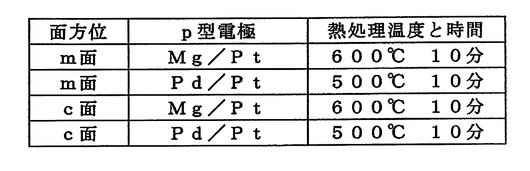
図7から明らかなように、Mg/Pt電極によれば、接触面がc面の場合でも、Pd/Pt電極に比べてコンタクト抵抗の若干の低減が観測された。しかし、m面の場合、Mg/Pt電極のコンタクト抵抗は、顕著に低下していることが判明した。 As is clear from FIG. 7, according to the Mg / Pt electrode, even when the contact surface is the c-plane, a slight reduction in contact resistance was observed compared to the Pd / Pt electrode. However, in the case of the m plane, it has been found that the contact resistance of the Mg / Pt electrode is significantly reduced.
次に、図8を参照しながら、コンタクト抵抗について熱処理温度の依存性を説明する。図8は、p型のGaN層のm面(以下、「m面GaN」と表記する)上に、Mg層、その上にPt層を形成した場合(すなわち、m面GaN(Mg/Pt))の結果を示している。また、対比として、p型のm面GaN層上にPd層、その上にPt層を形成した場合(m面GaN(Pd/Pt)、そして、p型のGaN層のc面(以下、「c面GaN」と表記する)上にPd層、その上にPt層を形成した場合(c面GaN(Pd/Pt))の結果も示している。p型GaN層には、いずれも、前述した濃度分布を有するようにMgがドーピングされている。 Next, the dependence of the heat treatment temperature on the contact resistance will be described with reference to FIG. FIG. 8 shows a case where an Mg layer is formed on an m-plane (hereinafter referred to as “m-plane GaN”) of a p-type GaN layer, and a Pt layer is formed thereon (that is, m-plane GaN (Mg / Pt)). ) Result. In contrast, when a Pd layer is formed on a p-type m-plane GaN layer and a Pt layer is formed thereon (m-plane GaN (Pd / Pt), and the c-plane of the p-type GaN layer (hereinafter, “ Also shown is the result when a Pd layer is formed on the c-plane GaN and a Pt layer is formed thereon (c-plane GaN (Pd / Pt)). Mg is doped so as to have a concentration distribution.
熱処理前における各層の厚さは、以下の表3に示す通りである。 The thickness of each layer before heat treatment is as shown in Table 3 below.

まず、Pd/Pt層の電極の場合、m面GaNのコンタクト抵抗は、c面GaNのコンタクト抵抗と比較して高い値となる。そして、m面およびc面GaNのいずれも500℃を超える熱処理温度においては、コンタクト抵抗の上昇が見られる。 First, in the case of an electrode of a Pd / Pt layer, the contact resistance of m-plane GaN is higher than that of c-plane GaN. In both m-plane and c-plane GaN, an increase in contact resistance is observed at a heat treatment temperature exceeding 500 ° C.
一方、m面GaN(Mg/Pt)の電極は、熱処理を行なわないときは、Pd/Ptの電極と比較してコンタクト抵抗は高い。これは、仕事関数が小さい金属の方がコンタクト抵抗が高いという技術常識と合致する。しかしながら、m面GaN(Mg/Pt)の電極の場合、熱処理温度を上げると共に、コンタクト抵抗が小さくなり、500℃の熱処理温度の場合には、m面GaN(Mg/Pt)のコンタクト抵抗は、m面GaN(Pd/Pt)のコンタクト抵抗と同等またはそれ以下となる。 On the other hand, the m-plane GaN (Mg / Pt) electrode has a higher contact resistance than the Pd / Pt electrode when heat treatment is not performed. This is consistent with the common technical knowledge that a metal having a lower work function has a higher contact resistance. However, in the case of an electrode of m-plane GaN (Mg / Pt), the heat treatment temperature is increased and the contact resistance is reduced. When the heat treatment temperature is 500 ° C., the contact resistance of m-plane GaN (Mg / Pt) is It becomes equal to or less than the contact resistance of m-plane GaN (Pd / Pt).
加えて、500℃を超えた温度(例えば、600℃)になると、m面GaN(Mg/Pt)のコンタクト抵抗は更に低下して、c面GaN(Mg/Pt)のコンタクト抵抗と同等となり、さらにはそれ以下になる。図8に示したグラフでは、おおよそ550℃以上になると、m面GaN(Mg/Pt)のコンタクト抵抗は、c面GaN(Mg/Pt)のコンタクト抵抗の値以下(またはそれ未満)になる。 In addition, when the temperature exceeds 500 ° C. (for example, 600 ° C.), the contact resistance of m-plane GaN (Mg / Pt) further decreases to be equivalent to the contact resistance of c-plane GaN (Mg / Pt), Even less. In the graph shown in FIG. 8, when the temperature is approximately 550 ° C. or higher, the contact resistance of m-plane GaN (Mg / Pt) becomes less than (or less than) the contact resistance of c-plane GaN (Mg / Pt).
600℃の温度では、m面GaN(Mg/Pt)のコンタクト抵抗は、600℃の温度でのm面およびc面GaN(Mg/Pt)のいずれのコンタクト抵抗よりも低くなり、具体的には、約1.0E-02Ωcm-2又はその周辺まで低下する。また、700℃の温度では、m面GaN(Mg/Pt)のコンタクト抵抗は、600℃の温度の場合よりも上昇するものの、700℃の温度でのm面およびc面GaN(Mg/Pt)のいずれのコンタクト抵抗よりも低くなる。 At a temperature of 600 ° C., the contact resistance of m-plane GaN (Mg / Pt) is lower than the contact resistance of both the m-plane and c-plane GaN (Mg / Pt) at a temperature of 600 ° C. Specifically, , About 1.0E-02 Ωcm −2 or its periphery. At 700 ° C., the contact resistance of m-plane GaN (Mg / Pt) is higher than that at 600 ° C., but the m-plane and c-plane GaN (Mg / Pt) at 700 ° C. It becomes lower than any of the contact resistances.
したがって、m面GaN(Mg/Pt)の熱処理温度としては、例えば、500℃以上が好ましい。700℃を超えて所定温度(例えば800℃)以上になると、電極やGaN層の膜質の劣化が進むため、上限は700℃以下が好ましい。そして、600℃近傍(例えば、600℃±50℃)がより好適な熱処理温度である。 Therefore, the heat treatment temperature of m-plane GaN (Mg / Pt) is preferably, for example, 500 ° C. or higher. When the temperature exceeds 700 ° C. and reaches a predetermined temperature (for example, 800 ° C.) or more, the film quality of the electrode and the GaN layer is deteriorated. The vicinity of 600 ° C. (for example, 600 ° C. ± 50 ° C.) is a more preferable heat treatment temperature.
次に、各温度で熱処理を行った後の電極の表面状態を示す写真を図9に示す。図9では、As-depo(熱処理を行なわない場合)、熱処理温度500℃、600℃、700℃の結果を示している。 Next, FIG. 9 shows a photograph showing the surface state of the electrode after heat treatment at each temperature. FIG. 9 shows the results of As-depo (when no heat treatment is performed) and heat treatment temperatures of 500 ° C., 600 ° C., and 700 ° C.
図9からわかるように、p型のc面GaN層の上にPd層、その上にPt層を形成した場合(C-GaN(Pd/Pt)の場合)は、500℃、600℃、700℃のどの熱処理においても金属表面の劣化は見られない。AFM測定による表面の算術平均粗さ(Ra)は500℃で約2nm、600℃で約2nm、700℃で約4nmとなった。 As can be seen from FIG. 9, when a Pd layer is formed on a p-type c-plane GaN layer and a Pt layer is formed thereon (in the case of C-GaN (Pd / Pt)), 500 ° C., 600 ° C., 700 ° C. There is no deterioration of the metal surface in any heat treatment at ℃. The arithmetic mean roughness (Ra) of the surface by AFM measurement was about 2 nm at 500 ° C., about 2 nm at 600 ° C., and about 4 nm at 700 ° C.
一方、p型のm面GaN層の上にPd層、その上にPt層を形成した場合(M-GaN(Pd/Pt)の場合)は、600℃、700℃の熱処理において金属表面の荒れが見られ、劣化が認められる。AFM測定によるRaは600℃で約30nm、700℃で約77nmとなった。すなわち、熱処理による電極の劣化が、m面GaNの電極に特有な課題であることがわかる。 On the other hand, when a Pd layer is formed on a p-type m-plane GaN layer and a Pt layer is formed thereon (in the case of M-GaN (Pd / Pt)), the surface of the metal is roughened by heat treatment at 600 ° C. and 700 ° C. Is observed and deterioration is observed. Ra by AFM measurement was about 30 nm at 600 ° C. and about 77 nm at 700 ° C. That is, it can be seen that electrode degradation due to heat treatment is a problem specific to m-plane GaN electrodes.
そして、p型のm面GaN層の上にMg層、その上にPt層を形成した場合(M-GaN(Mg/Pt)の場合)は、700℃の熱処理温度では僅かに凹凸は見られるものの、500℃、600℃、700℃の全ての熱処理温度において電極が劣化しないことが確認された。AFM測定による表面のRaは500℃で約1.5nm、600℃で約1.5nm、700℃で約4.5nmとなり、良好な表面状態が得られた。そして、本実施形態の構成において、電極の表面のRaは、約4.5nm以下であることが好ましく、約1.5nm以下であることがさらに好ましい。 When the Mg layer is formed on the p-type m-plane GaN layer and the Pt layer is formed thereon (in the case of M-GaN (Mg / Pt)), slight unevenness is observed at a heat treatment temperature of 700 ° C. However, it was confirmed that the electrode did not deteriorate at all the heat treatment temperatures of 500 ° C., 600 ° C., and 700 ° C. The surface Ra by AFM measurement was about 1.5 nm at 500 ° C., about 1.5 nm at 600 ° C., and about 4.5 nm at 700 ° C., and a good surface state was obtained. In the configuration of this embodiment, the Ra of the electrode surface is preferably about 4.5 nm or less, and more preferably about 1.5 nm or less.
さらに、GaN層上にMg層(30nm)を形成し、800℃および900℃で10分間熱処理した場合のGaN層のフォトルミネッセンス測定結果を図10に示す。図10(a)は、800℃で熱処理した結果を示し、そして、図10(b)は、900℃で熱処理した結果を示している。図10(a)及び(b)中の縦軸のPL強度は、フォトルミネッセンス強度の意味である。図10(a)および(b)のグラフには、それぞれ、熱処理前に得られたPL強度(「Ref」と表記する曲線)が示されている。 Furthermore, FIG. 10 shows the photoluminescence measurement results of the GaN layer when an Mg layer (30 nm) is formed on the GaN layer and heat-treated at 800 ° C. and 900 ° C. for 10 minutes. 10A shows the result of heat treatment at 800 ° C., and FIG. 10B shows the result of heat treatment at 900 ° C. The PL intensity on the vertical axis in FIGS. 10A and 10B means the photoluminescence intensity. In the graphs of FIGS. 10A and 10B, the PL intensity (curve denoted as “Ref”) obtained before the heat treatment is shown.
まず、本願発明者の実験によると、700℃以下の熱処理では、熱処理前と後でフォトルミネッセンスのスペクトルの変化は見られなかった。一方、図10(a)に示すように、800℃の場合では、530nm付近にイエローバンドと呼ばれる、空孔欠陥に起因すると考えられる発光が見られるようになる。さらに熱処理温度を上げると、図10(b)に示すように、530nm付近の発光は強度を増し、空孔欠陥の密度の増加を示す。これよりMg層を用いた電極における熱処理温度は、GaNの品質の保持という観点から、700℃以下にすることが望ましい。 First, according to the experiment by the inventors of the present application, in the heat treatment at 700 ° C. or lower, no change in the photoluminescence spectrum was observed before and after the heat treatment. On the other hand, as shown in FIG. 10A, in the case of 800 ° C., light emission considered to be caused by a vacancy defect called a yellow band is seen near 530 nm. When the heat treatment temperature is further increased, as shown in FIG. 10B, the emission near 530 nm increases in intensity and increases in the density of vacancy defects. Accordingly, the heat treatment temperature in the electrode using the Mg layer is desirably 700 ° C. or lower from the viewpoint of maintaining the quality of GaN.
次に、図11に、電極構造(Mg/Pt)においてMg原子の深さ方向のプロファイルを、SIMS(Secondary Ion-microprobe Mass Spectrometer)を用いて得た結果を示す。図11(a)は、Mg層をGaN層上に形成した構成(Mg/Pt電極)において、熱処理を行なわない場合(as-depo)の結果を示し、一方、図11(b)は、熱処理後の結果を示している。なお、熱処理の温度および時間は、c面GaNの場合に600℃で10分、m面GaNの場合に600℃で10分および630℃で10分である。 Next, FIG. 11 shows the result of obtaining the profile of Mg atoms in the depth direction in the electrode structure (Mg / Pt) by using a secondary-ion-microprobe-mass-spectrometer (SIMS). FIG. 11 (a) shows the result when the heat treatment is not performed (as-depo) in the configuration in which the Mg layer is formed on the GaN layer (Mg / Pt electrode), while FIG. 11 (b) shows the heat treatment. Later results are shown. The temperature and time of the heat treatment are 10 minutes at 600 ° C. for c-plane GaN, 10 minutes at 600 ° C. and 10 minutes at 630 ° C. for m-plane GaN.
いずれの電極においても、熱処理前におけるMg層厚は7nmであり、Pt層厚は75nmである。 In any electrode, the Mg layer thickness before the heat treatment is 7 nm, and the Pt layer thickness is 75 nm.
図11(a)、図11(b)のグラフの縦軸は、Mg濃度であり、横軸は、深さ方向の距離である。横軸の数値が「-」の領域は電極側であり、「+」の領域はp型GaN側である。横軸の原点(0μm)は、Mgのピーク位置であり、p型GaN層とMg層との界面の位置にほぼ相当する。これらの事項は、後に説明する図12、図13、図15のグラフでも同様である。 11A and 11B, the vertical axis represents the Mg concentration, and the horizontal axis represents the distance in the depth direction. The region where the numerical value on the horizontal axis is “−” is the electrode side, and the region “+” is the p-type GaN side. The origin (0 μm) on the horizontal axis is the peak position of Mg and substantially corresponds to the position of the interface between the p-type GaN layer and the Mg layer. These matters also apply to the graphs of FIGS. 12, 13, and 15 described later.
図11(a)、(b)のグラフにおいて、「◆」は、c面GaN上に形成した熱処理温度が600℃のサンプルに関するデータを示している。また、グラフ中の「△」は、m面GaN上に形成した熱処理温度が600℃のサンプルに関するデータを示し、「○」は、m面GaN上に形成した熱処理温度が630℃のサンプルに関するデータを示している。後述する図12、図13、図15のグラフにおいても、同様である。なお、熱処理前のp型GaN層には、いずれも、前述した通り、電極が接触するp型GaN層の表面から深さ20nmの領域に7×1019cm-3のMgがドーピングされ、それよりも深い領域には1×1019cm-3のMgがドーピングされている。
In the graphs of FIGS. 11A and 11B, “♦” indicates data related to a sample having a heat treatment temperature of 600 ° C. formed on c-plane GaN. Further, “Δ” in the graph indicates data related to a sample formed on m-plane GaN with a heat treatment temperature of 600 ° C., and “◯” indicates data related to a sample formed on m-plane GaN having a heat treatment temperature of 630 ° C. Is shown. The same applies to the graphs of FIGS. 12, 13, and 15 described later. As described above, the p-type GaN layer before the heat treatment is doped with 7 × 10 19 cm −3 Mg in a
図11(a)に示すように、as-depoの場合は、m面GaNにおいても、c面GaNにおいてもMgのプロファイルに変化は無い。一方、図11(b)に示すように、GaN層の上にMg層を形成後に熱処理を行った場合には、それぞれ、Mgのプロファイルは大きく異なるものとなった。 As shown in FIG. 11A, in the case of as-depo, there is no change in the Mg profile in both the m-plane GaN and the c-plane GaN. On the other hand, as shown in FIG. 11B, when the heat treatment was performed after the Mg layer was formed on the GaN layer, the Mg profiles differed greatly.
熱処理を行った場合には、図11(b)に示すように、c面GaN上のMgは、p型GaN層にかなりの濃度で拡散していることが見られる。また、Pt層にもMgが拡散していることが見られる。一方、m面GaN上のMgは、p型GaN層にも、Pt層にも拡散はほとんどしていないことが確認される。さらに詳述すると、c面GaNの場合、熱処理後にはMgがPt層に奥深く拡散し、そして、GaN側にも奥深く拡散している。一方、m面GaNの場合、熱処理後にはMgがPt層側に僅かに拡散するものの、GaN側には殆ど拡散しないものであった。これは、600℃であっても630℃であってもほとんど差異が無かった。このように、熱処理の前と後で、c面GaN上のMgの拡散と、m面GaN上のMgの拡散との間に顕著な差が生じる。その理由は未だ不明であるが、c面とm面との最表面原子の配列、極性の違いや原子の緻密さに起因するものと推測される。 When heat treatment is performed, it can be seen that Mg on the c-plane GaN diffuses in the p-type GaN layer at a considerable concentration, as shown in FIG. It can also be seen that Mg is diffused in the Pt layer. On the other hand, it is confirmed that Mg on the m-plane GaN hardly diffuses in the p-type GaN layer and the Pt layer. More specifically, in the case of c-plane GaN, Mg diffuses deeply into the Pt layer after heat treatment, and also diffuses deeply into the GaN side. On the other hand, in the case of m-plane GaN, Mg slightly diffuses to the Pt layer side after heat treatment, but hardly diffuses to the GaN side. This was almost the same at 600 ° C. and 630 ° C. Thus, there is a significant difference between Mg diffusion on c-plane GaN and Mg diffusion on m-plane GaN before and after heat treatment. The reason for this is still unclear, but is presumed to be due to the arrangement of the outermost surface atoms between the c-plane and the m-plane, the difference in polarity, and the atomic density.
図12は、電極構造(Mg/Pt)においてGa原子の深さ方向のプロファイルを、SIMSを用いて得た結果を示す。熱処理前におけるMg層厚は7nmであり、Pt層厚は75nmである。グラフの縦軸は原子濃度と比例関係にある、SIMSの検出器の信号強度を示す。図12における横軸の距離0μmはp型GaN層とMg層との界面の位置にほぼ相当する。なお、横軸の原点(0μm)は、Mgピークの位置に合わせた。横軸の数値が「-」の領域は電極側であり、「+」の領域はp型GaN側である。縦軸は、as-depoのGaN結晶中のGa濃度を1として規格化している。また母体の原子密度から算定すると、縦軸の強度の1×10-3は濃度として1×1019cm-3にほぼ相当する。
FIG. 12 shows the result of obtaining a profile in the depth direction of Ga atoms in the electrode structure (Mg / Pt) using SIMS. The Mg layer thickness before heat treatment is 7 nm, and the Pt layer thickness is 75 nm. The vertical axis of the graph shows the signal intensity of the SIMS detector, which is proportional to the atomic concentration. The
図12(a)は、Mg層をGaN層上に形成した構成(Mg/Pt電極)において、熱処理を行なわない場合(as-depo)の結果を示し、一方、図12(b)は、熱処理後の結果を示している。なお、図12(b)では、熱処理温度が600℃と630℃との2種類の結果を示している。熱処理の温度および時間は、c面GaNの場合に600℃で10分、m面GaNの場合に600℃で10分および630℃で10分である。 FIG. 12 (a) shows the result when heat treatment is not performed (as-depo) in the configuration in which the Mg layer is formed on the GaN layer (Mg / Pt electrode), while FIG. 12 (b) shows the heat treatment. Later results are shown. In FIG. 12B, two types of results with heat treatment temperatures of 600 ° C. and 630 ° C. are shown. The temperature and time of the heat treatment are 10 minutes at 600 ° C. for c-plane GaN, 10 minutes at 600 ° C. and 10 minutes at 630 ° C. for m-plane GaN.
図12(a)に示すように、as-depoの場合は、m面GaNにおいても、c面GaNにおいてもGaのプロファイルに変化は無い。一方、図12(b)に示すように、GaN層の上にMg層を形成後に熱処理を行った場合には、Gaのプロファイルは異なるものとなった。 As shown in FIG. 12A, in the case of as-depo, there is no change in the Ga profile in both the m-plane GaN and the c-plane GaN. On the other hand, as shown in FIG. 12B, when heat treatment was performed after the Mg layer was formed on the GaN layer, the Ga profile was different.
具体的には、図12(b)に示すように、熱処理を行った場合はMg層中にGaが拡散していることが確認された。m面GaN上にMg層を形成して600℃で熱処理を行った試料では、Mg層中にGaの拡散が認められ、コンタクト抵抗も低くなる。その原因の詳細は不詳ではあるが、Mg層中のGa拡散量とコンタクト抵抗との間の相関があることが確認された。 Specifically, as shown in FIG. 12B, it was confirmed that Ga was diffused in the Mg layer when heat treatment was performed. In a sample in which an Mg layer is formed on m-plane GaN and heat-treated at 600 ° C., Ga diffusion is observed in the Mg layer, and the contact resistance is low. Although details of the cause are unknown, it has been confirmed that there is a correlation between the amount of Ga diffusion in the Mg layer and the contact resistance.
さらに詳述すると、c面GaNの場合は、GaがMg層およびPt層中に拡散し、GaN結晶中の奥からもGaが電極中に移動している。換言すると、c面GaNの場合、Gaは全体的にGaN層から電極中に顕著に拡散している。一方、m面GaNでは、熱処理温度が600℃の場合、c面GaNとは異なり、界面近傍のみでGa原子が移動しているようである。c面と比べてm面では原子が動きにくい状況にあると推測される。ただし、m面GaNの場合でも、熱処理温度が630℃の場合は、GaがMg層およびPt層の全体に拡散している。なお、m面コンタクト抵抗は熱処理温度が600℃の場合の方が630℃の場合によりも低い。これは、熱処理温度が600℃の場合、後述するようにm面では窒素が拡散しにくく、その結果、Gaの空孔がアクセプターとして機能するのに対し、熱処理温度が630℃の場合は、600℃の場合に比べ、より多くの窒素原子が電極側へ拡散するためではないかと考えられる。 More specifically, in the case of c-plane GaN, Ga diffuses into the Mg layer and Pt layer, and Ga also moves into the electrode from the back in the GaN crystal. In other words, in the case of c-plane GaN, Ga is diffused significantly from the GaN layer into the electrode as a whole. On the other hand, in m-plane GaN, when the heat treatment temperature is 600 ° C., unlike c-plane GaN, Ga atoms seem to move only near the interface. It is presumed that atoms are less likely to move on the m-plane than on the c-plane. However, even in the case of m-plane GaN, when the heat treatment temperature is 630 ° C., Ga diffuses throughout the Mg layer and the Pt layer. The m-plane contact resistance is lower when the heat treatment temperature is 600 ° C. than when it is 630 ° C. This is because when the heat treatment temperature is 600 ° C., nitrogen hardly diffuses in the m-plane as will be described later. As a result, Ga vacancies function as acceptors, whereas when the heat treatment temperature is 630 ° C., 600 Compared to the case of ° C., more nitrogen atoms may be diffused to the electrode side.
図13(a)は、熱処理前のMg/Pt電極における窒素原子の深さ方向プロファイルを示すグラフであり、図13(b)は、熱処理後におけるMg/Pt電極における窒素原子の深さ方向プロファイルを示すグラフである。熱処理前におけるMg層厚は7nmであり、Pt層厚は75nmである。図13(a)、図13(b)のグラフの縦軸は、N強度であり、横軸は、深さ方向の距離である。1×10-3のN強度は1×1019cm-3のN濃度にほぼ相当する。横軸の数値が「-」の領域は電極側であり、「+」の領域はp型GaN側である。横軸の原点(0μm)は、p型GaN層とMg層との界面の位置にほぼ相当する。電極の構造およびp型GaNのドーピング条件は、図11を参照して説明したサンプルにおけるものと同様である。 FIG. 13A is a graph showing a profile in the depth direction of nitrogen atoms in the Mg / Pt electrode before the heat treatment, and FIG. 13B is a profile in the depth direction of nitrogen atoms in the Mg / Pt electrode after the heat treatment. It is a graph which shows. The Mg layer thickness before heat treatment is 7 nm, and the Pt layer thickness is 75 nm. 13A and 13B, the vertical axis represents the N intensity, and the horizontal axis represents the distance in the depth direction. N intensity of 1 × 10 -3 corresponds approximately to the N concentration of 1 × 10 19 cm -3. The region where the numerical value on the horizontal axis is “−” is the electrode side, and the region “+” is the p-type GaN side. The origin (0 μm) on the horizontal axis substantially corresponds to the position of the interface between the p-type GaN layer and the Mg layer. The electrode structure and p-type GaN doping conditions are the same as those in the sample described with reference to FIG.
蒸着後、熱処理を行なわないサンプルでは、図13(a)に示すように、c面GaNに対する電極およびm面GaNに対する電極の両方において、いずれも窒素原子が電極側に拡散していないことがわかる。 In the sample that is not heat-treated after vapor deposition, as shown in FIG. 13 (a), it can be seen that in both the electrode for c-plane GaN and the electrode for m-plane GaN, nitrogen atoms are not diffused to the electrode side. .
一方、熱処理後におけるc面GaNに対する電極では、図13(b)に示すように、窒素原子が電極側に拡散していることが確認された。しかし、熱処理後におけるm面GaNに対する電極では、窒素原子は電極側にほとんど拡散していない。すなわち、m面GaNでは、Ga原子のみが電極側に拡散し、窒素原子は拡散していない。これに対し、c面GaNでは、Ga原子も窒素原子も電極側に拡散している。p型GaNにおいてGaが電極側に拡散すると、p型GaNの最表面でGa原子が不足する状態、すなわちGa空孔が形成される。Ga空孔はアクセプター的性質を有するため、電極とp型GaNとの界面の近傍でGa空孔が増加すると、この界面のショットキー障壁を正孔がトンネリングによって通過しやすくなる。しかし、Ga原子とともに窒素原子も電極側に拡散すると、p型GaNの最表面に窒素の不足する状態、すなわち窒素空孔も形成される。窒素空孔はドナー的性質を有し、Ga空孔との間で電荷補償を起こす。このため、c面GaNのようにGaのみならず窒素も電極側に拡散すると、コンタクト抵抗の低下は特に生じなくなる。 On the other hand, in the electrode for the c-plane GaN after the heat treatment, it was confirmed that nitrogen atoms were diffused to the electrode side as shown in FIG. However, in the electrode for m-plane GaN after the heat treatment, nitrogen atoms are hardly diffused on the electrode side. That is, in m-plane GaN, only Ga atoms diffuse to the electrode side, and nitrogen atoms do not diffuse. In contrast, in c-plane GaN, both Ga atoms and nitrogen atoms are diffused to the electrode side. When Ga diffuses to the electrode side in p-type GaN, a state where Ga atoms are insufficient on the outermost surface of p-type GaN, that is, Ga vacancies are formed. Since Ga vacancies have an acceptor property, when Ga vacancies increase near the interface between the electrode and p-type GaN, holes easily pass through the Schottky barrier at this interface by tunneling. However, when nitrogen atoms diffuse together with Ga atoms to the electrode side, a nitrogen deficient state, that is, nitrogen vacancies are also formed on the outermost surface of p-type GaN. Nitrogen vacancies have donor properties and cause charge compensation with Ga vacancies. For this reason, when not only Ga but nitrogen is diffused to the electrode side like c-plane GaN, the contact resistance is not particularly lowered.
次に、Mg層におけるN(窒素)濃度とGa濃度との関係について詳述する。図12(b)に示すように、600℃にて熱処理を行った場合、m面GaN層上のMg層におけるGaのSIMS検出濃度は4×1.0E-02となった。SIMSの検出強度はその原子濃度に比例する。従って、GaN層の母体のGa濃度が1×1022cm-3程度と仮定した場合、Mg層中に4×1019cm-3程度のGaが存在しているものと考えられる。630℃にて熱処理を行った場合は、SIMSの検出強度は3×1.0E-02となった。同様の仮定により、m面GaN層上のMg層中には3×1019cm-3程度のGaが存在するものと考えられる。 Next, the relationship between the N (nitrogen) concentration and the Ga concentration in the Mg layer will be described in detail. As shown in FIG. 12B, when heat treatment was performed at 600 ° C., the SIMS detected concentration of Ga in the Mg layer on the m-plane GaN layer was 4 × 1.0E-02. The detected intensity of SIMS is proportional to the atomic concentration. Therefore, when it is assumed that the Ga concentration of the base material of the GaN layer is about 1 × 10 22 cm −3 , it is considered that Ga of about 4 × 10 19 cm −3 exists in the Mg layer. When heat treatment was performed at 630 ° C., the SIMS detection intensity was 3 × 1.0E-02. Based on the same assumption, it is considered that Ga of about 3 × 10 19 cm −3 exists in the Mg layer on the m-plane GaN layer.
一方、図13(b)に示すように、600℃及び630℃で熱処理を行った場合のどちらも、m面GaN層上のMg層におけるN(窒素)のSIMS検出濃度は、検出感度の限界である1×1.0E-03となった。同様の仮定により、m面GaN層上のMg層中に含まれるN(窒素)は1×1018cm-3以下と考えられる。以上より、m面GaN層上のMg層中のGa原子濃度は、N原子濃度より1桁(10倍)以上大きい。 On the other hand, as shown in FIG. 13B, the SIMS detection concentration of N (nitrogen) in the Mg layer on the m-plane GaN layer is the limit of detection sensitivity when heat treatment is performed at 600 ° C. and 630 ° C. 1 × 1.0E-03. Based on the same assumption, N (nitrogen) contained in the Mg layer on the m-plane GaN layer is considered to be 1 × 10 18 cm −3 or less. From the above, the Ga atom concentration in the Mg layer on the m-plane GaN layer is one digit (10 times) or more higher than the N atom concentration.
これに対し、c面GaN層上のMg層では、Ga及びNは、SIMS検出強度はいずれも1E-2であり、いずれも1×1019cm-3程度存在するものと考えられる。すなわち、c面GaN層上のMg層中におけるGa原子とN原子の濃度はほぼ同程度である。 On the other hand, in the Mg layer on the c-plane GaN layer, it is considered that Ga and N both have SIMS detection intensity of 1E-2 and both are present at about 1 × 10 19 cm −3 . That is, the concentrations of Ga atoms and N atoms in the Mg layer on the c-plane GaN layer are approximately the same.
なお、このような各元素(Mg、Ga、N、Pt)の挙動は、Mg層が接触するGaN層において、Gaの一部がAlやInで置換されていても同様に生じると推定される。また、Mg層が接触するGaN系半導体層中にドーパントとしてMg以外の元素がドープされている場合でも同様であると推定される。 In addition, it is estimated that such behavior of each element (Mg, Ga, N, Pt) occurs similarly even if a part of Ga is substituted with Al or In in the GaN layer in contact with the Mg layer. . In addition, it is presumed that the same is true even when an element other than Mg is doped as a dopant in the GaN-based semiconductor layer in contact with the Mg layer.
次に、図14に、m面GaN層上にMg層を形成した電極構造(Mg/Pt)の断面透過電子顕微鏡(TEM)写真を示す。図14(a)は、熱処理を行なわない場合(as-depo)の結果を示している。図14(b)は、600℃で10分間の熱処理後の結果を示している。 Next, FIG. 14 shows a cross-sectional transmission electron microscope (TEM) photograph of an electrode structure (Mg / Pt) in which an Mg layer is formed on an m-plane GaN layer. FIG. 14A shows the result when no heat treatment is performed (as-depo). FIG. 14B shows the result after heat treatment at 600 ° C. for 10 minutes.
この例では、図14(a)に示すように、7nm厚のMg層をGaN結晶上に形成した。図14(b)に示すように、熱処理後はPt層がMg層に浸食し、Mg層の厚さが2nmとなった。 In this example, as shown in FIG. 14A, a 7 nm thick Mg layer was formed on the GaN crystal. As shown in FIG. 14B, the Pt layer eroded into the Mg layer after the heat treatment, and the thickness of the Mg layer became 2 nm.
図14(b)からわかるように、Mg層(図3(a)中の層32)の厚さは薄い(例えば、2nm)とはいえ、Pt層(図3(a)中の層34)によって合金化ないしは吸収されていないMgからなるMg層(図3(a)中の層32)の存在が確認された。この薄層のMg層(32)の存在が、従来技術では非常にコンタクト抵抗が大きかったm面GaNのコンタクト抵抗を低減できる主要な要因の一つと推測される。
As can be seen from FIG. 14B, the Mg layer (the
次に、図15に、電極構造(Mg/Pt)においてPtの深さ方向のプロファイルを、SIMSを用いて得た結果を示す。図15(a)および(b)は、上述のSIMSと同様に、それぞれ、熱処理を行なわない場合(as-depo)、および、熱処理後の結果である。熱処理前におけるMg層厚は7nmであり、Pt層厚は75nmである。図15(a)、(b)のグラフの縦軸は、Pt強度であり、横軸は、深さ方向の距離である。1×10-3のPt強度は1×1019cm-3のPt濃度にほぼ相当する。横軸の数値が「-」の領域は電極側であり、「+」の領域はp型GaN側である。横軸の原点(0μm)は、p型GaN層とMg層との界面の位置にほぼ相当する。電極の構造およびp型GaNのドーピング条件は、図11を参照して説明したサンプルにおけるものと同様である。 Next, FIG. 15 shows the result of obtaining a profile in the depth direction of Pt in the electrode structure (Mg / Pt) using SIMS. FIGS. 15A and 15B show the results when heat treatment is not performed (as-depo) and after the heat treatment, respectively, as in the above-described SIMS. The Mg layer thickness before heat treatment is 7 nm, and the Pt layer thickness is 75 nm. 15A and 15B, the vertical axis represents the Pt intensity, and the horizontal axis represents the distance in the depth direction. Pt intensity of 1 × 10 -3 corresponds approximately to a Pt concentration of 1 × 10 19 cm -3. The region where the numerical value on the horizontal axis is “−” is the electrode side, and the region “+” is the p-type GaN side. The origin (0 μm) on the horizontal axis substantially corresponds to the position of the interface between the p-type GaN layer and the Mg layer. The electrode structure and p-type GaN doping conditions are the same as those in the sample described with reference to FIG.
図15(a)に示すように、as-depoの場合は、m面GaNにおいても、c面GaNにおいてもPtのプロファイルに変化は無い。一方、図15(b)に示すように、熱処理後は、c面GaNにおいてPtはGaN側に拡散していることがわかる。しかしながら、m面GaNにおいてはPtプロファイルに変化はほとんど無く、GaN層中にPtが拡散していないことが確認された。より詳述すると、c面GaNの場合、熱処理後においてPtはMg層側に大きく拡散する。一方、m面GaNの場合、熱処理後においてPtはMg層側に僅かに拡散しただけであった(c面GaNの1/10程度)。熱処理温度が600℃であっても630℃でもほとんど差異が無かった。 As shown in FIG. 15A, in the case of as-depo, there is no change in the profile of Pt in both the m-plane GaN and the c-plane GaN. On the other hand, as shown in FIG. 15B, it can be seen that Pt diffuses to the GaN side in the c-plane GaN after the heat treatment. However, there was almost no change in the Pt profile in m-plane GaN, and it was confirmed that Pt was not diffused in the GaN layer. More specifically, in the case of c-plane GaN, Pt largely diffuses to the Mg layer side after heat treatment. On the other hand, in the case of m-plane GaN, Pt was only slightly diffused to the Mg layer side after heat treatment (about 1/10 of c-plane GaN). There was almost no difference even when the heat treatment temperature was 600 ° C or 630 ° C.
このことは、本実施形態の構成(Mg/Pt)においては、GaN層と接触する領域においてはMgとの合金化がAuの場合と比較して顕著には起こっていないことを意味している。 This means that in the configuration of the present embodiment (Mg / Pt), alloying with Mg does not occur significantly in the region in contact with the GaN layer compared to the case of Au. .
m面GaN上に厚さ2nmのMg層を形成した後、600℃で10分間の熱処理を行った試料を作製した。この試料の断面について、透過電子顕微鏡(TEM)による観察を行った。図16(a)は、熱処理前におけるMg/Pt電極構造を示す模式図である。図16(b)は、熱処理前におけるMg/Pt電極構造を示す模式図である。いずれの図面も、断面TEMに基づいて作成した。 A sample was prepared by forming a Mg layer having a thickness of 2 nm on m-plane GaN and then performing heat treatment at 600 ° C. for 10 minutes. The cross section of this sample was observed with a transmission electron microscope (TEM). FIG. 16A is a schematic diagram showing the Mg / Pt electrode structure before the heat treatment. FIG. 16B is a schematic diagram showing the Mg / Pt electrode structure before the heat treatment. All drawings were prepared based on the cross-sectional TEM.
Mg層の堆積時の厚さが5nmを超える場合、600℃で10分間の熱処理によってMg層の厚さは減少するが、熱処理の後もMg層は実質的に連続した膜として存在する。しかし、Mg層の堆積時の厚さが2nm程度になると、600℃で10分間の熱処理の後、図16(b)に示すように、MgとPtとの合金形成に消費されなかったMgがアイランド状に存在する場合のあることが確認された。堆積直後のMg層の厚さが2nm程度になると、行なう熱処理の条件によって、最終的に得られるMg層のモフォロジーは多様であり得る。 When the thickness of the deposited Mg layer exceeds 5 nm, the thickness of the Mg layer is reduced by the heat treatment at 600 ° C. for 10 minutes, but the Mg layer exists as a substantially continuous film even after the heat treatment. However, when the thickness at the time of deposition of the Mg layer is about 2 nm, after heat treatment at 600 ° C. for 10 minutes, as shown in FIG. It was confirmed that the islands may exist. When the thickness of the Mg layer immediately after deposition is about 2 nm, the morphology of the finally obtained Mg layer may be varied depending on the conditions of the heat treatment to be performed.
なお、本明細書における「Mg層」とは、p型半導体領域の表面に存在する多数のアイランド状(島状)Mgの集まりをも含むものとする。また、この「Mg層」は、複数の開口部が存在する膜(例えばポーラスな膜)から構成されていても良い。このように、Ptに浸食されないMgがp型半導体領域の表面(m面)と接触していれば、コンタクト抵抗低減効果を充分に得ることができる。 Note that the “Mg layer” in this specification includes a collection of a large number of island-like (island-like) Mg existing on the surface of the p-type semiconductor region. Further, the “Mg layer” may be composed of a film having a plurality of openings (for example, a porous film). Thus, if Mg that is not eroded by Pt is in contact with the surface (m-plane) of the p-type semiconductor region, a contact resistance reduction effect can be sufficiently obtained.
なお、Pt層の代わりに、Mo層またはPd層をMg層上に堆積した場合も、ほぼ同様の結果(コンタクト抵抗低減効果)が得られると考えられる。コンタクト抵抗低減効果を得るという観点から重要な点は、Mg層とGaN系半導体とが接触することと、Mg層上の金属がAuと比較してMgと合金を形成し難い材料から形成されていることにある。 In addition, it is considered that substantially the same result (contact resistance reduction effect) can be obtained when a Mo layer or a Pd layer is deposited on the Mg layer instead of the Pt layer. The important point from the viewpoint of obtaining the contact resistance reduction effect is that the Mg layer and the GaN-based semiconductor are in contact with each other, and the metal on the Mg layer is formed from a material that is difficult to form an alloy with Mg as compared with Au. There is to be.
次に、再び図3(a)を参照しながら、本実施形態の構成をさらに詳述する。 Next, the configuration of this embodiment will be described in further detail with reference to FIG.
図3(a)に示すように、本実施形態の発光素子100では、m面GaN基板10と、基板10上に形成されたAluGavInwN層(u+v+w=1, u≧0, v≧0, w≧0)22とが形成されている。この例では、m面GaN基板10は、n型GaN基板(例えば、厚さ、100μm)であり、AluGavInwN層22は、n型GaN層(例えば、厚さ2μm)である。AluGavInwN層22の上には活性層24が形成されている。言い換えると、m面GaN基板10の上には、少なくとも活性層24を含む半導体積層構造20が形成されている。
As shown in FIG. 3A, in the
半導体積層構造20において、AlxGayInzN層22の上には、AlaInbGacN層(a+b+c=1,a≧0, b≧0, c≧0)を含む活性層24が形成されている。活性層24は、例えば、In組成比が約25%のInGaN井戸層とGaNバリア層で構成され、井戸層の厚さは9nm、バリア層の厚さは9nm、井戸層周期は3周期である。活性層24の上には、第2導電型(p型)のAldGaeN層(d+e=1, d≧0, e≧0)26が形成されている。第2導電型(p型)のAldGaeN層(d+e=1, d≧0, e≧0)26は例えば、Al組成比が10%のAlGaN層で厚さは0.2μmである。本実施形態のAldGaeN層26には、p型のドーパントとして、Mgがドープされている。ここでMgは、AldGaeN層26に対して、例えば、1018cm-3程度ドープされている。またこの例では、活性層24とAldGaeN層26との間に、アンドープのGaN層(不図示)が形成されている。
In the semiconductor stacked
さらに、この例においては、AldGaeN層26の上には、第2導電型(例えば、p型)のGaN層(不図示)が形成されている。さらに、p+-GaNからなるコンタクト層上には、Mg層32が形成されており、その上にPt層34が形成されている。このMg層32とPt層34の積層構造が電極(p型電極)30となる。
Further, in this example, a second conductivity type (for example, p-type) GaN layer (not shown) is formed on the Al d Ga e N layer 26. Further, an
なお、半導体積層構造20には、AluGavInwN層22の表面を露出させる凹部(リセス)42が形成されており、凹部42の底面に位置するAluGavInwN層22には、電極(n型電極)40が形成されている。凹部42の大きさは、例えば、幅(または径)20μmであり、深さは1μmである。電極40は、例えば、Ti層とAl層とPt層(例えば、厚さはそれぞれ、5nm、100nm、10nm)の積層構造から成る電極である。
Note that the
本実施形態の窒化物系半導体発光素子100によれば、動作電圧(Vop)を、従来のPd/Pt電極を用いたm面LEDの場合よりも約1.5V低減させることができ、その結果、消費電力を低減できることがわかった。
According to the nitride-based semiconductor
次に、引き続き図3(a)を参照しながら、本実施形態の窒化物系半導体発光素子100の製造方法を説明する。
Next, a method for manufacturing the nitride-based semiconductor light-emitting
まず、m面基板10を用意する。本実施形態では、基板10として、GaN基板を用いる。本実施形態のGaN基板は、HVPE(Hydride Vapor Phase Epitaxy)法を用いて得られる。
First, an m-
例えば、まずc面サファイア基板上に数mmオーダの厚膜GaNを成長する。その後、厚膜GaNをc面に垂直方向、m面で切り出すことによりm面GaN基板が得られる。GaN基板の作製方法は、上記に限らず、例えばナトリウムフラックス法などの液相成長やアモノサーマル法などの融液成長方法を用いてバルクGaNのインゴットを作製し、それをm面で切り出す方法でも良い。 For example, first, a thick film GaN on the order of several mm is grown on a c-plane sapphire substrate. Then, an m-plane GaN substrate is obtained by cutting the thick film GaN in the direction perpendicular to the c-plane and the m-plane. The production method of the GaN substrate is not limited to the above, and a method of producing an ingot of bulk GaN using a liquid phase growth method such as a sodium flux method or a melt growth method such as an ammonothermal method, and cutting it in the m plane But it ’s okay.
基板10としては、GaN基板の他、例えば、酸化ガリウム、SiC基板、Si基板、サファイア基板などを用いることができる。基板上にm面から成るGaN系半導体をエピタキシャル成長するためには、SiCやサファイア基板の面方位もm面である方が良い。ただし、r面サファイア基板上にはa面GaNが成長するという事例もあることから、成長条件によっては必ずしも成長用表面がm面であることが必須とならない場合もあり得る。少なくとも半導体積層構造20の表面がm面であれば良い。本実施形態では、基板10の上に、MOCVD(Metal Organic Chemical Vapor Deposition)法により結晶層を順次形成していく。
As the
次に、m面GaN基板10の上に、AluGavInwN層22を形成する。AluGavInwN層22として、例えば、厚さ3μmのAlGaNを形成する。GaNを形成する場合には、m面GaN基板10の上に、1100℃でTMG(Ga(CH3)3)、TMA(Al(CH3)3)およびNH3を供給することによってGaN層を堆積する。
Next, an Al u Ga v In w N layer 22 is formed on the m-
次に、AluGavInwN層22の上に、活性層24を形成する。この例では、活性層24は、厚さ9nmのGa0.9In0.1N井戸層と、厚さ9nmのGaNバリア層が交互に積層された厚さ81nmのGaInN/GaN多重量子井戸(MQW)構造を有している。Ga0.9In0.1N井戸層を形成する際には、Inの取り込みを行なうために、成長温度を800℃に下げることが好ましい。
Next, the
次に、活性層24の上に、例えば厚さ30nmのアンドープGaN層を堆積する。次いで、アンドープGaN層の上に、AldGaeN層26を形成する。AldGaeN層26として、例えば、TMG、NH3、TMA、TMIおよびp型不純物としてCp2Mg(シクロペンタジエニルマグネシウム)を供給することにより、厚さ70nmのp-Al0.14Ga0.86Nを形成する。
Next, an undoped GaN layer having a thickness of 30 nm, for example, is deposited on the
次に、AldGaeN層26の上に、例えば厚さ0.5μmのp-GaNコンタクト層を堆積する。p-GaNコンタクト層を形成する際には、p型不純物としてCp2Mgを供給する。 Next, a p-GaN contact layer having a thickness of 0.5 μm, for example, is deposited on the Al d Ga e N layer 26. When forming the p-GaN contact layer, Cp 2 Mg is supplied as a p-type impurity.
その後、塩素系ドライエッチングを行なうことにより、p-GaNコンタクト層、AldGaeN層26、アンドープGaN層および活性層24の一部を除去して凹部42を形成し、AlxGayInzN層22のn型電極形成領域を露出させる。次いで、凹部42の底部に位置するn型電極形成領域の上に、n型電極40として、Ti/Pt層を形成する。
Thereafter, by performing chlorine-based dry etching, the p-GaN contact layer, the Al d Ga e N layer 26, the undoped GaN layer, and a part of the
さらに、p-GaNコンタクト層の上には、Mg層32を形成し、さらにMg層32上にPt層34を形成する。これにより、p型電極40を形成する。本実施形態では、Mg層32の形成に原料金属をパルス的に蒸発させながら蒸着を行なう手法(パルス蒸着法)を用いている。より具体的には、真空中(例えば、5×10-6Torr)に保持したるつぼ中のMg金属に、パルス的に電子ビームを照射し、パルス的に原料金属を蒸発させる。その原料金属分子または原子がp-GaNコンタクト層に付着し、Mg層32が形成される。パルスは例えばパルス幅0.5秒、繰り返し1Hzである。パルス幅は0.005秒以上5秒以下、パルス周波数は0.1Hz以上100Hz以下であることが好ましい。このような手法により、Mg層32として緻密で良好な品質の膜が形成された。Mg層が緻密になる理由は、パルス的な蒸着を行なうことにより、p-GaNコンタクト層に衝突するMg原子またはMg原子クラスタの運動エネルギーが増加するためであると考えられる。すなわち、電子ビームの照射によって、原料Mgの一部が瞬間的に高エネルギーを持ったMg原子となって気化あるいは蒸発する。そして、Mg原子はp-GaNコンタクト層へ到達する。p-GaNコンタクト層へ到達したMg原子はマイグレーションを起こし、原子レベルで緻密で均質なMg薄膜を形成する。1パルスの電子ビームによって、1~20原子層程度のMg薄膜が形成される。パルス状の電子ビームを繰り返し照射することによってMg薄膜がp-GaNコンタクト層に積層され、所望の厚さのMg層32が形成される。電子ビームは、Mg原子が吸着後にマイグレーションを起こすのに必要な運動エネルギーをMg原子に供給することができるよう、高いピーク強度を有していることが好ましい。また、電子ビームの1パルスあたり、20原子層(およそ5nm)以下の厚さでMg薄膜が形成されるように電子銃の駆動パワーを決定することが好ましい。電子ビームの1パルスあたりに形成されるMg薄膜が20原子層よりも厚くなると、緻密で均質なMg薄膜が得られにくくなる。より好ましい堆積速度は、電子ビームの1パルスあたり、5原子層以下である。これはMg原子が多すぎると、Mg原子がマイグレーション中にぶつかり合い、それによりMg原子が持つ運動エネルギーが失われてしまうからである。
Further, an
一般にMgは水や空気との接触により酸化されやすい元素である。通常の蒸着方法によって支持基板上に形成したMg薄膜を大気中に置いた場合、速やかに酸化される。この結果、Mg薄膜は次第に金属光沢を失い、最終的にはボロボロとなって支持体から剥がれ落ちる。これに対し、本実施形態の形成方法(パルス蒸着)によって作成されたMg層32は、原子レベルで緻密で均質であり、エピタキシャル成長させたように非常に原子配列の整った構造を有している。そして、酸化の原因と考えられるピンホールは殆ど存在せず、酸化されにくい。大気中に数ヶ月放置してもきれいな鏡面を保持することができる。
Generally, Mg is an element that is easily oxidized by contact with water or air. When an Mg thin film formed on a support substrate by a normal vapor deposition method is placed in the atmosphere, it is rapidly oxidized. As a result, the Mg thin film gradually loses metallic luster and eventually becomes tattered and peels off from the support. On the other hand, the
また、一般にMgはその融点を超えると一気に気化してしまう性質を有する。このため、Mg薄膜の堆積速度を調整することによって、形成するMg薄膜の厚さをナノメートルオーダーで正確に制御することが非常に困難である。これに対し、本実施形態の形成方法によって作成されたMg層32は、パルス状電子ビームの照射時間等を適宜設定することで、その厚さをナノメートルオーダーで正確に制御できる。
In general, Mg has the property of being vaporized at once when its melting point is exceeded. For this reason, it is very difficult to accurately control the thickness of the Mg thin film to be formed on the nanometer order by adjusting the deposition rate of the Mg thin film. On the other hand, the thickness of the
なお、本実施形態の形成方法は、Si基板やガラス基板上にMg薄膜を形成する場合にも有効である。よって、本実施形態の形成方法はGaNに限らず、様々な種類の物質上にMg薄膜を形成できる。そして、本実施形態の形成方法は、特に半導体分野における電極の形成に好適に用いることができる。また、本実施形態の形成方法は、Mg蒸着時にMg薄膜が形成される基板や支持体を加熱する必要がない。このため、加熱ができない、あるいは、加熱しにくい形状の基板や支持体の上であっても、室温程度で緻密で均質なMg薄膜の形成が可能である。 Note that the forming method of the present embodiment is also effective when an Mg thin film is formed on a Si substrate or a glass substrate. Therefore, the formation method of this embodiment is not limited to GaN, and an Mg thin film can be formed on various types of materials. And the formation method of this embodiment can be used suitably especially for formation of the electrode in the semiconductor field | area. Moreover, the formation method of this embodiment does not need to heat the board | substrate and support body in which Mg thin film is formed at the time of Mg vapor deposition. Therefore, a dense and homogeneous Mg thin film can be formed at about room temperature even on a substrate or support that has a shape that cannot be heated or is difficult to heat.
また、本実施形態の形成方法によって作成されたMg層32は、600℃以上の温度で熱処理を行っても安定である。
Further, the
なお、本実施形態では、原料金属(Mg金属)をパルス的に蒸発させながら蒸着を行なう手法を採用しているが、Mg層32を形成できるのであれば、他の手法を採用することも可能である。緻密で良質なMg層を形成する他の手法としては、例えば熱CVD法や分子線エピタキシ(MBE)などを採用することが可能である。
In this embodiment, a technique of performing vapor deposition while vaporizing the source metal (Mg metal) in a pulsed manner is adopted, but other techniques can be adopted as long as the
なお、その後、レーザリフトオフ、エッチング、研磨などの方法を用いて、基板10、AluGavInwN層22の一部までを除去してもよい。この場合、基板10のみを除去してもよいし、基板10およびAluGavInwN層22の一部だけを選択的に除去してもよい。もちろx、基板10、AluGavInwN層22を除去せずに残してもよい。以上の工程により、本実施形態の窒化物系半導体発光素子100が形成される。
Thereafter, the
本実施形態の窒化物系半導体発光素子100において、n型電極40とp型電極30との間に電圧を印加すると、p型電極30から活性層24に向かって正孔が、n型電極40から活性層24に向かって電子が注入され、例えば450nm波長の発光が生じる。
In the nitride-based semiconductor
ここで、図17(a)に、m面GaN上にMg/Pt層からなる電極を用いた発光ダイオードの電流-電圧特性を示す。比較のため、発光ダイオードの窒化物系半導体の構造は同じで、Pd/Pt層からなる電極を用いた発光ダイオードの特性、及びc面GaN上にMg/Pt層からなる電極を用いた発光ダイオードの特性を示す。これら3種類の発光ダイオードにおける電極の構成および熱処理条件は、以下の表4に示す通りである。 Here, FIG. 17A shows current-voltage characteristics of a light emitting diode using an electrode made of an Mg / Pt layer on m-plane GaN. For comparison, the nitride semiconductor structure of the light emitting diode is the same, the characteristics of the light emitting diode using the electrode made of the Pd / Pt layer, and the light emitting diode using the electrode made of the Mg / Pt layer on the c-plane GaN The characteristics of The electrode configuration and heat treatment conditions in these three types of light emitting diodes are as shown in Table 4 below.

この発光ダイオードの構成は、m面またはc面GaN基板上に、n型GaN層、InGaN井戸層(3層)とGaNバリア層(2層)とが交互に積層された活性層、p型GaN層が積層されたものである。さらにp型GaN層上にはp型電極として、Mg/Pt電極またはPd/Pt電極を設けている。n型電極は、p型GaN層、活性層をエッチングし、n型GaN層を露出させ、n型GaN層上に形成している。 This light-emitting diode has a configuration in which an n-type GaN layer, an InGaN well layer (three layers) and a GaN barrier layer (two layers) are alternately stacked on an m-plane or c-plane GaN substrate, p-type GaN Layers are stacked. Further, an Mg / Pt electrode or a Pd / Pt electrode is provided as a p-type electrode on the p-type GaN layer. The n-type electrode is formed on the n-type GaN layer by etching the p-type GaN layer and the active layer to expose the n-type GaN layer.
図17(a)から明らかなように、電流が0ボルトから増加しても、電流値がほぼゼロの状態が続くが、印加電圧があるレベル(立ち上がり電圧)を超えると、電流値は電圧の増加に伴って増加する。立ち上がり電圧は、Pd/Pt層からなる電極(m面GaN上)の場合、約3.1Vである。これに対し、Mg/Pt層からなる電極(m面GaN上)の場合の立ち上がり電圧は、約2.5Vとなり、低減が見られる。縦軸の電流値が20mAとなる動作電圧は、Mg/Pt層からなる電極ではPd/Pt層からなる電極と比較し、1.5V以上低減していることが確認される。 As is clear from FIG. 17A, even when the current increases from 0 volts, the current value continues to be almost zero, but when the applied voltage exceeds a certain level (rising voltage), the current value becomes the voltage value. It increases with the increase. The rising voltage is about 3.1 V in the case of an electrode (on m-plane GaN) made of a Pd / Pt layer. On the other hand, the rising voltage in the case of the electrode (on the m-plane GaN) made of the Mg / Pt layer is about 2.5 V, and a reduction is observed. It is confirmed that the operating voltage at which the current value on the vertical axis is 20 mA is reduced by 1.5 V or more in the electrode made of the Mg / Pt layer compared to the electrode made of the Pd / Pt layer.
次に、m面GaN上Mg/Pt層からなる電極を用いた発光ダイオード(m面発光ダイオード)とc面GaN上Mg/Pt層からなる電極を用いた発光ダイオード(c面発光ダイオード)との比較を行う。m面発光ダイオードにおいては、立ち上がり電圧がc面発光ダイオードと比較し低く、コンタクト抵抗の低減効果が確認される。例えば、m面発光ダイオードにおいては駆動電圧3.2Vにおいて電流値は20mAが得られる。一方、c面発光ダイオードにおいては同じ駆動電圧では4.8mAの電流値となる。発光ダイオードの光出力は電流値に依存することから、駆動電圧3.2Vにおいてm面発光ダイオードにおいては、c面発光ダイオードの4倍近くの光出力が得られることが分かる。 Next, a light-emitting diode (m-plane light-emitting diode) using an electrode made of an Mg / Pt layer on m-plane GaN and a light-emitting diode (c-plane light-emitting diode) using an electrode made of an Mg / Pt layer on c-plane GaN Make a comparison. In the m-plane light emitting diode, the rising voltage is lower than that of the c-plane light emitting diode, and the effect of reducing the contact resistance is confirmed. For example, in an m-plane light emitting diode, a current value of 20 mA is obtained at a driving voltage of 3.2 V. On the other hand, the c-surface light emitting diode has a current value of 4.8 mA at the same driving voltage. Since the light output of the light emitting diode depends on the current value, it can be seen that the m-plane light emitting diode can obtain a light output nearly four times that of the c surface light emitting diode at the driving voltage of 3.2 V.
また、電流値-電圧特性を示す曲線の傾きは、Pd/Pt電極を有する素子に比べ、Mg/Pt電極を有する素子の方が急である。発光ダイオードは、内部にp-n接合を有するダイオードであり、p-n接合ダイオードの電流-電圧特性を示す曲線は、一般に以下の式で近似される。
I=I0exp(V/n・KT)
ここで、Iはp-n接合ダイオードを流れる電流値、I0は電流定数、Vは印加電圧、Kはボルツマン定数、Tは温度、nはダイオードの理想度合いを示すn値である。実験は室温で行ったため、KT=0.025(V)である。
In addition, the slope of the curve indicating the current value-voltage characteristic is steeper in the element having the Mg / Pt electrode than in the element having the Pd / Pt electrode. A light-emitting diode is a diode having a pn junction therein, and a curve indicating current-voltage characteristics of a pn junction diode is generally approximated by the following equation.
I = I 0 exp (V / n · KT)
Here, I is a current value flowing through a pn junction diode, I 0 is a current constant, V is an applied voltage, K is a Boltzmann constant, T is a temperature, and n is an n value indicating the ideal degree of the diode. Since the experiment was performed at room temperature, KT = 0.025 (V).
p-n接合ダイオードのn値は、電流-電圧特性を示す曲線の傾きから決定される。理想的なp-n接合ダイオードの場合、n=1であるが、現実のp-n接合ダイオードでは、n値は1から異なっている。n値は1に近いほど好ましい。本実験によれば、Mg/Pt電極を有する素子の場合、n=1.4となり、Pd/Pt電極を有する素子の場合、n=2.2であった。このことからわかるように、Mg/Pt電極を用いることにより、優れたダイオード特性を実現できる。 The n value of the pn junction diode is determined from the slope of the curve indicating the current-voltage characteristics. In the case of an ideal pn junction diode, n = 1, but in an actual pn junction diode, the n value is different from 1. The n value is preferably closer to 1. According to this experiment, n = 1.4 in the case of the element having the Mg / Pt electrode, and n = 2.2 in the case of the element having the Pd / Pt electrode. As can be seen from this, excellent diode characteristics can be realized by using the Mg / Pt electrode.
図17(b)に示すように、この発光ダイオードのコンタクト抵抗の値は、Mg/Pt層からなる電極では3.8×10-4Ωcm2の値が得られた。このような10のマイナス4乗台のコンタクト抵抗の値は、p型のm面GaNにおいては、はじめての例であり、これは驚異的な結果である。これによって消費電力を低減できることがわかった。加えて、m面GaN素子において、極めて大きな技術的意義を提供できることが見出された。なお、Pd/Pt層からなる電極では、約1×10-2Ωcm2の値であった。
As shown in FIG. 17B, the value of the contact resistance of this light emitting diode was 3.8 × 10 −4 Ωcm 2 for the electrode made of the Mg / Pt layer. Such a contact resistance value of 10
次に、図18を参照しながら、Au層、および、Mg/Au層からなる電極を用いた例(比較例)について説明する。図18(a)は、m面のGaN層の上に、Au層、または、Mg/Au層の電極を形成し、その固有コンタクト抵抗(Ω・cm2)を測定した結果を示している。なお、この固有コンタクト抵抗は、電極を形成して熱処理を行った後の固有コンタクト抵抗の値である。 Next, an example (comparative example) using an electrode made of an Au layer and an Mg / Au layer will be described with reference to FIG. FIG. 18A shows the result of forming an Au layer or Mg / Au layer electrode on an m-plane GaN layer and measuring its specific contact resistance (Ω · cm 2 ). The specific contact resistance is a value of the specific contact resistance after the electrode is formed and heat treatment is performed.
図18(a)の結果からわかるように、Au層の電極に比べ、Mg/Au層の電極を用いた場合の方が固有コンタクト抵抗の特性は悪化する。この点、本実施形態の電極(例えば、Mg/Pt層)の構成における特性向上の結果と顕著に相違する。なお、上述したように、Mgは水や空気との接触により酸化されやすい元素であるので、Mg層の単独での電極では無くAu層の積層体(Mg/Au層)として使用される構成は検討候補の一つに成り得る。しかしながら、実際には、Au層と比較してMg/Au層のコンタクト抵抗は増加するがゆえに、コンタクト特性は悪い。換言すると、本実施形態の構成(例えば、Mg/Pt層)のコンタクト抵抗の特性が優れていることは、Mg層にAu層を積層した場合の結果が悪かったことに鑑みると、当業者にとって予見できない効果を有していたと思われる。 As can be seen from the result of FIG. 18A, the characteristic of the specific contact resistance is worse when the Mg / Au layer electrode is used than when the Au layer electrode is used. This point is significantly different from the result of the characteristic improvement in the configuration of the electrode (for example, Mg / Pt layer) of the present embodiment. As described above, since Mg is an element that is easily oxidized by contact with water or air, the structure used as a laminate of Mg layers (Mg / Au layer) instead of a single electrode of Mg layer is Can be one of the candidates for consideration. However, in reality, the contact resistance of the Mg / Au layer is increased as compared with the Au layer, so that the contact characteristics are poor. In other words, the excellent contact resistance characteristics of the configuration of the present embodiment (for example, the Mg / Pt layer) is that the results of the case where the Au layer is stacked on the Mg layer are bad for those skilled in the art. It seems to have had an unpredictable effect.
また、図18(b)は、熱処理後のMg/Au層の電極の表面を示す図面代用写真であり、一方、図18(c)は、熱処理後のAu層の電極の表面を示す図面代用写真である。両者を比べると、Mg/Au層の電極の方の膜質が悪いことがわかった。 FIG. 18B is a drawing-substituting photograph showing the surface of the Mg / Au layer electrode after the heat treatment, while FIG. 18C is a drawing-substituting photograph showing the surface of the Au layer electrode after the heat treatment. It is a photograph. When both were compared, it was found that the film quality of the Mg / Au layer electrode was worse.
次に、図19を参照する。図19は、Conicalチップによる硬度マッピング(5mN、1μm conical)を表している。図19(a)はc面GaN基板(C-GaN)の結果を示し、そして、図19(b)はm面GaN基板(M-GaN)の結果を示している。両者を比較すると、m面GaN基板の方が、硬度が低いことがわかった。なお、このようなm面GaN基板とc面GaN基板との物性の違いが、本実施形態の電極構成(例えば、Mg層/Pt層)の特性に影響を与えている可能性もあり得る。 Next, refer to FIG. FIG. 19 shows hardness mapping (5 mN, 1 μm conical) using a Conical chip. FIG. 19A shows the result of the c-plane GaN substrate (C-GaN), and FIG. 19B shows the result of the m-plane GaN substrate (M-GaN). When both were compared, it was found that the m-plane GaN substrate had lower hardness. It should be noted that such a difference in physical properties between the m-plane GaN substrate and the c-plane GaN substrate may possibly affect the characteristics of the electrode configuration (eg, Mg layer / Pt layer) of the present embodiment.
以上、本発明を好適な実施形態により説明してきたが、こうした記述は限定事項では無く、勿論、種々の改変が可能である。 As described above, the present invention has been described with reference to the preferred embodiments. However, such description is not a limitation, and various modifications can be made.
なお、本発明の実施形態と本質的に構成を異にするものであるが、関連する構造が特許文献3、4に開示されている。しかしながら、特許文献3および4には、窒化ガリウム系半導体層の結晶面がm面であることの記載は一切無く、したがって、これらの文献の開示はc面の窒化ガリウム系半導体層の上に電極を形成した技術に関するものである。特に、特許文献3は、Mg層の上にAu層を積層した構成に関するものであり、その積層構造の電極を仮にm面上に形成したとしても、本実施形態の電極の効果が得られるものでは無い。また、特許文献4は、Ni、Cr、Mgからなる金属層に言及しているが、開示されている実施例はNi層を下層にした電極構造を有しているもののみである。特許文献3、4とも、c面の窒化ガリウム系半導体層の上に形成された電極構造に関するものであり、m面の窒化ガリウム系半導体層に対するコンタクト抵抗に関する問題も解決策も教示されていない。
In addition, although the configuration is essentially different from the embodiment of the present invention, related structures are disclosed in
本発明に係る上記の発光素子は、そのまま光源として使用されても良い。しかし、本発明に係る発光素子は、波長変換のための蛍光物質を備える樹脂などと組み合わせれば、波長帯域の拡大した光源(例えば白色光源)として好適に使用され得る。 The light emitting device according to the present invention may be used as a light source as it is. However, the light-emitting element according to the present invention can be suitably used as a light source (for example, a white light source) having an extended wavelength band when combined with a resin or the like including a fluorescent material for wavelength conversion.
図20は、このような白色光源の一例を示す模式図である。図20の光源は、図3(a)に示す構成を有する発光素子100と、この発光素子100から放射された光の波長を、より長い波長に変換する蛍光体(例えばYAG:Yttrium Alumninum Garnet)が分散された樹脂層200とを備えている。発光素子100は、表面に配線パターンが形成された支持部材220上に搭載されており、支持部材220上には発光素子100を取り囲むように反射部材240が配置されている。樹脂層200は、発光素子100を覆うように形成されている。
FIG. 20 is a schematic diagram showing an example of such a white light source. The light source of FIG. 20 includes a
なお、Mg層32と接触するp型半導体領域がGaN、もしくはAlGaNから構成される場合について説明したが、Inを含む層、例えばInGaNであってもよい。この場合、Inの組成を例えば0.2とした「In0.2Ga0.8N」を、電極30と接するコンタクト層に用いることができる。GaNにInを含ませることにより、AlaGabN(a+b=1,a≧0, b>0)のバンドギャップをGaNのバンドギャップよりも小さくできるため、コンタクト抵抗を低減することができる。以上のことから、Mg層が接するp型半導体領域は、AlxInyGazN(x+y+z=1,x≧0, y≧0, z≧0)半導体から形成されていればよい。
Although the case where the p-type semiconductor region in contact with the
コンタクト抵抗低減の効果は、当然に、LED以外の発光素子(半導体レーザ)や、発光素子以外のデバイス(例えばトランジスタや受光素子)においても得ることが可能である。 The effect of reducing the contact resistance can naturally be obtained in light emitting elements (semiconductor lasers) other than LEDs and devices other than light emitting elements (for example, transistors and light receiving elements).
実際のm面半導体層の表面(主面)は、m面に対して完全に平行な面である必要は無く、m面から僅かな角度(0度より大きく±1°未満)で傾斜していても良い。表面がm面に対して完全に平行な表面を有する基板や半導体層を形成することは、製造技術の観点から困難である。このため、現在の製造技術によってm面基板やm面半導体層を形成した場合、現実の表面は理想的なm面から傾斜してしまう。傾斜の角度および方位は、製造工程によってばらつくため、表面の傾斜角度および傾斜方位を正確に制御することは難しい。なお、基板や半導体の表面(主面)をm面から1°以上の角度で傾斜させることを意図的に行う場合がある。以下に説明する実施形態における窒化ガリウム系化合物半導体発光素子は、m面から1°以上の角度で傾斜した面を主面とするp型半導体領域を備えている。 The actual surface (main surface) of the m-plane semiconductor layer does not need to be a plane that is completely parallel to the m-plane, and is inclined at a slight angle (greater than 0 ° and less than ± 1 °) from the m-plane. May be. It is difficult to form a substrate or a semiconductor layer having a surface that is completely parallel to the m-plane from the viewpoint of manufacturing technology. For this reason, when an m-plane substrate or an m-plane semiconductor layer is formed by the current manufacturing technology, the actual surface is inclined from the ideal m-plane. Since the inclination angle and orientation vary depending on the manufacturing process, it is difficult to accurately control the inclination angle and inclination orientation of the surface. In some cases, the surface (main surface) of the substrate or semiconductor is intentionally inclined at an angle of 1 ° or more from the m-plane. The gallium nitride-based compound semiconductor light-emitting element in the embodiment described below includes a p-type semiconductor region having a main surface that is inclined at an angle of 1 ° or more from the m-plane.
(他の実施形態)
図21は、本実施形態の窒化ガリウム系化合物半導体発光素子100aを示す断面図である。m面から1°以上の角度で傾斜した面を主面とするp型半導体領域を形成するため、本実施形態に係る窒化ガリウム系化合物半導体発光素子100aは、m面から1°以上の角度で傾斜した面を主面とするGaN基板10aを用いている。主面がm面から1°以上の角度で傾斜している基板は、一般に「オフ基板」と称される。オフ基板は、単結晶インゴットから基板をスライスし、基板の表面を研磨する工程で、意図的にm面から特定方位に傾斜した面を主面とするように作製され得る。このGaN基板10a上に、半導体積層構造20aを形成する。図21に示す半導体層22a、24a、26aは主面がm面から1°以上の角度で傾斜している。これは傾斜した基板の主面上に、各種半導体層が積層されると、これらの半導体層の表面(主面)もm面から傾斜するからである。GaN基板10aの代わりに、例えば、m面から特定方向に傾斜した面を表面とするサファイア基板やSiC基板を用いてもよい。
(Other embodiments)
FIG. 21 is a cross-sectional view showing the gallium nitride compound semiconductor
次に、図22~図26を参照しながら、本実施形態におけるp型半導体領域の傾斜について詳細を説明する。 Next, details of the inclination of the p-type semiconductor region in this embodiment will be described with reference to FIGS.
図22(a)は、GaN系化合物半導体の結晶構造(ウルツ鉱型結晶構造)を模式的に示す図であり、図2の結晶構造の向きを90°回転させた構造を示している。GaN結晶のc面には、+c面および-c面が存在する。+c面はGa原子が表面に現れた(0001)面であり、「Ga面」と称される。一方、-c面はN(窒素)原子が表面に現れた(000-1)面であり、「N面」と称される。+c面と-c面とは平行な関係にあり、いずれも、m面に対して垂直である。c面は、極性を有するため、このように、c面を+c面と-c面に分けることができるが、非極性面であるa面を、+a面と-a面に区別する意義はない。 FIG. 22 (a) is a diagram schematically showing a crystal structure (wurtzite crystal structure) of a GaN-based compound semiconductor, and shows a structure obtained by rotating the crystal structure of FIG. 2 by 90 °. There are a + c plane and a −c plane on the c-plane of the GaN crystal. The + c plane is a (0001) plane in which Ga atoms appear on the surface, and is referred to as a “Ga plane”. On the other hand, the −c plane is a (000-1) plane in which N (nitrogen) atoms appear on the surface, and is referred to as an “N plane”. The + c plane and the −c plane are parallel to each other, and both are perpendicular to the m plane. Since the c-plane has polarity, the c-plane can be divided into a + c-plane and a −c-plane in this way, but there is no significance in distinguishing the non-polar a-plane into the + a-plane and the −a-plane. .
図22(a)に示す+c軸方向は、-c面から+c面に垂直に延びる方向である。一方、a軸方向は、図2の単位ベクトルa2に対応し、m面に平行な[-12-10]方向を向いている。図22(b)は、m面の法線、+c軸方向、およびa軸方向の相互関係を示す斜視図である。m面の法線は、[10-10]方向に平行であり、図22(b)に示されるように、+c軸方向およびa軸方向の両方に垂直である。 The + c-axis direction shown in FIG. 22A is a direction extending perpendicularly from the −c plane to the + c plane. On the other hand, the a-axis direction corresponds to the unit vector a 2 in FIG. 2 and faces the [-12-10] direction parallel to the m-plane. FIG. 22B is a perspective view showing the correlation between the normal of the m-plane, the + c-axis direction, and the a-axis direction. The normal of the m-plane is parallel to the [10-10] direction and is perpendicular to both the + c-axis direction and the a-axis direction, as shown in FIG.
GaN系化合物半導体層の主面がm面から1°以上の角度で傾斜するということは、この半導体層の主面の法線がm面の法線から1°以上の角度で傾斜することを意味する。 The fact that the main surface of the GaN-based compound semiconductor layer is inclined at an angle of 1 ° or more from the m-plane means that the normal line of the main surface of the semiconductor layer is inclined at an angle of 1 ° or more from the normal line of the m-plane. means.
次に、図23を参照する。図23(a)および(b)は、それぞれ、GaN系化合物半導体層の主面およびm面の関係を示す断面図である。この図は、m面およびc面の両方に垂直な断面図である。図23には、+c軸方向を示す矢印が示されている。図23に示したように、m面は+c軸方向に対して平行である。従って、m面の法線ベクトルは、+c軸方向に対して垂直である。 Next, refer to FIG. FIGS. 23A and 23B are cross-sectional views showing the relationship between the main surface and the m-plane of the GaN-based compound semiconductor layer, respectively. This figure is a cross-sectional view perpendicular to both the m-plane and the c-plane. FIG. 23 shows an arrow indicating the + c-axis direction. As shown in FIG. 23, the m-plane is parallel to the + c-axis direction. Accordingly, the normal vector of the m-plane is perpendicular to the + c axis direction.
図23(a)および(b)に示す例では、GaN系化合物半導体層における主面の法線ベクトルが、m面の法線ベクトルからc軸方向に傾斜している。より詳細に述べれば、図23(a)の例では、主面の法線ベクトルは+c面の側に傾斜しているが、図23(b)の例では、主面の法線ベクトルは-c面の側に傾斜している。本明細書では、前者の場合におけるm面の法線べクトルに対する主面の法線ベクトルの傾斜角度(傾斜角度θ)を正の値にとり、後者の場合における傾斜角度θを負の値にとることにする。いずれの場合でも、「主面はc軸方向に傾斜している」といえる。 23A and 23B, the normal vector of the main surface in the GaN-based compound semiconductor layer is inclined in the c-axis direction from the normal vector of the m-plane. More specifically, in the example of FIG. 23 (a), the normal vector of the principal surface is inclined toward the + c plane, whereas in the example of FIG. 23 (b), the normal vector of the principal surface is − Inclined to the c-plane side. In the present specification, the inclination angle (inclination angle θ) of the normal vector of the principal surface with respect to the normal vector of the m plane in the former case is a positive value, and the inclination angle θ in the latter case is a negative value. I will decide. In either case, it can be said that “the main surface is inclined in the c-axis direction”.
本実施形態では、p型半導体領域の傾斜角度が1°以上5°以下の範囲、および、傾斜角度が-5°以上-1°以下の範囲にあるので、p型半導体領域の傾斜角度が0°より大きく±1°未満の場合と同様に本発明の効果を奏することができる。以下、図24を参照しながら、この理由を説明する。図24(a)および(b)は、それぞれ、図23(a)および(b)に対応する断面図であり、m面からc軸方向に傾斜したp型半導体領域における主面の近傍領域を示している。傾斜角度θが5°以下の場合には、図24(a)および(b)に示すように、p型半導体領域の主面に複数のステップが形成される。各ステップは、単原子層分の高さ(2.7Å)を有し、ほぼ等間隔(30Å以上)で平行に並んでいる。このようなステップの配列により、全体としてm面から傾斜した主面が形成されるが、微視的には多数のm面領域が露出していると考えられる。 In the present embodiment, since the inclination angle of the p-type semiconductor region is in the range of 1 ° to 5 ° and the inclination angle is in the range of −5 ° to −1 °, the inclination angle of the p-type semiconductor region is 0. The effect of the present invention can be obtained in the same manner as in the case of greater than ° and less than ± 1 °. Hereinafter, this reason will be described with reference to FIG. FIGS. 24A and 24B are cross-sectional views corresponding to FIGS. 23A and 23B, respectively, and show the vicinity of the main surface in the p-type semiconductor region inclined in the c-axis direction from the m-plane. Show. When the inclination angle θ is 5 ° or less, as shown in FIGS. 24A and 24B, a plurality of steps are formed on the main surface of the p-type semiconductor region. Each step has a height equivalent to a monoatomic layer (2.7 mm) and is arranged in parallel at substantially equal intervals (30 mm or more). By such an arrangement of steps, a main surface inclined from the m-plane as a whole is formed, but it is considered that a large number of m-plane regions are exposed microscopically.
図25は、m面から-c軸方向に1°傾斜したp型半導体領域の断面TEM写真である。p型半導体領域の表面には、m面が明確に表出しており、傾斜は原子ステップによって形成されていることが確認される。主面がm面から傾斜したGaN系化合物半導体層の表面がこのような構造となるのは、m面がもともと結晶面として非常に安定だからである。同様の現象は、主面の法線ベクトルの傾斜方向が+c面および-c面以外の面方位を向いていても生じると考えられる。主面の法線ベクトルが例えばa軸方向に傾斜していても、傾斜角度が1°以上5°以下の範囲にあれば同様であると考えられる。 FIG. 25 is a cross-sectional TEM photograph of the p-type semiconductor region tilted by 1 ° from the m-plane in the −c-axis direction. The m-plane is clearly exposed on the surface of the p-type semiconductor region, and it is confirmed that the inclination is formed by atomic steps. The surface of the GaN-based compound semiconductor layer whose main surface is inclined from the m-plane has such a structure because the m-plane is originally very stable as a crystal plane. A similar phenomenon is considered to occur even if the inclination direction of the normal vector of the main surface is oriented to a plane orientation other than the + c plane and the −c plane. Even if the normal vector of the main surface is inclined in the a-axis direction, for example, the same can be considered if the inclination angle is in the range of 1 ° to 5 °.
以上より、p型窒化ガリウム系化合物半導体層の表面(主面)をm面から1°以上の角度で傾斜している場合であっても、p型電極に接触する面は多数のm面領域が露出しているため、コンタクト抵抗は傾斜角に依存しないものと考えられる。 As described above, even when the surface (main surface) of the p-type gallium nitride compound semiconductor layer is inclined at an angle of 1 ° or more from the m-plane, the surface in contact with the p-type electrode has a large number of m-plane regions. Therefore, it is considered that the contact resistance does not depend on the inclination angle.
図26は、m面から-c軸方向に0°、2°、または5°傾斜したp型半導体領域の上にMg/Pt層の電極を形成し、そのコンタクト抵抗(Ω・cm2)を測定した結果を示すグラフである。グラフの縦軸は固有コンタクト抵抗、横軸は傾斜角度(m面の法線とp型半導体領域における表面の法線とが形成する角度)θである。なお、この固有コンタクト抵抗は、電極を形成して熱処理を行った後の固有コンタクト抵抗の値である。図26の結果から分かるように、傾斜角度θが5°以下であれば、コンタクト抵抗は、ほぼ一定の値となる。 In FIG. 26, an Mg / Pt layer electrode is formed on a p-type semiconductor region inclined by 0 °, 2 °, or 5 ° in the −c axis direction from the m-plane, and the contact resistance (Ω · cm 2 ) is shown. It is a graph which shows the measurement result. The vertical axis of the graph is the specific contact resistance, and the horizontal axis is the inclination angle (angle formed by the normal of the m-plane and the normal of the surface in the p-type semiconductor region) θ. The specific contact resistance is a value of the specific contact resistance after the electrode is formed and heat treatment is performed. As can be seen from the results in FIG. 26, when the inclination angle θ is 5 ° or less, the contact resistance has a substantially constant value.
以上から、p型半導体領域の表面の傾斜角度θが5°以下であれば、本発明の構成によりコンタクト抵抗は低減されることが確認された。 From the above, it was confirmed that the contact resistance is reduced by the configuration of the present invention when the inclination angle θ of the surface of the p-type semiconductor region is 5 ° or less.
なお、傾斜角度θの絶対値が5°より大きくなると、ピエゾ電界によって内部量子効率が低下する。このため、ピエゾ電界が顕著に発生するのであれば、m面成長により半導体発光素子を実現することの意義が小さくなる。したがって、本発明では、傾斜角度θの絶対値を5°以下に制限する。しかし、傾斜角度θを例えば5°に設定した場合でも、製造ばらつきにより、現実の傾斜角度θは5°から±1°程度ずれる可能性がある。このような製造ばらつきを完全に排除することは困難であり、また、この程度の微小な角度ずれは、本発明の効果を妨げるものでもない。 In addition, when the absolute value of the inclination angle θ is larger than 5 °, the internal quantum efficiency is lowered by the piezoelectric field. For this reason, if a piezo electric field is remarkably generated, the significance of realizing a semiconductor light emitting device by m-plane growth is reduced. Therefore, in the present invention, the absolute value of the inclination angle θ is limited to 5 ° or less. However, even when the inclination angle θ is set to 5 °, for example, the actual inclination angle θ may be shifted from 5 ° by about ± 1 ° due to manufacturing variations. It is difficult to completely eliminate such manufacturing variations, and such a small angular deviation does not hinder the effects of the present invention.
本実施の形態における半導体発光素子においても、蛍光物質を備える樹脂と組み合わせて、波長帯域の拡大した光源(例えば白色光源)として好適に使用され得る。 Also in the semiconductor light emitting device in this embodiment, it can be suitably used as a light source (for example, a white light source) having an extended wavelength band in combination with a resin including a fluorescent material.
本発明によれば、m面基板上で結晶成長させたGaN系半導体素子、または、m面を表面とするGaN系半導体積層構造体において、そのコンタクト抵抗を低減することができる。したがって、従来、コンタクト抵抗の特性の悪さから積極的な利用が困難であった、m面基板上で結晶成長させたGaN系半導体素子(または、m面を表面とするGaN系半導体積層構造体)の産業上の利用可能性が向上する。 According to the present invention, the contact resistance can be reduced in a GaN-based semiconductor element crystal-grown on an m-plane substrate or a GaN-based semiconductor multilayer structure having an m-plane as a surface. Therefore, GaN-based semiconductor elements grown on crystals on m-plane substrates (or GaN-based semiconductor multilayer structures with m-plane surfaces), which have been difficult to actively use due to poor contact resistance characteristics, have been heretofore used. The industrial availability of
10 基板(GaN系基板)
12 基板の表面(m面)
20 半導体積層構造
22 AluGavInwN層
24 活性層
26 AldGaeN層
30 p型電極
32 Mg層
34 金属層(Pt層)
40 n型電極
42 凹部
100 窒化物系半導体発光素子
200 樹脂層
220 支持部材
240 反射部材
10 Substrate (GaN-based substrate)
12 Substrate surface (m-plane)
20
40 N-
Claims (34)
前記p型半導体領域上に設けられた電極とを備え、
前記p型半導体領域は、AlxInyGazN(x+y+z=1,x≧0, y≧0, z≧0)半導体から形成され、
前記p型半導体領域は、m面から1°以上の角度で傾斜している半導体層であり、前記p型半導体領域における主面の法線とm面の法線とが形成する角度が1°以上5°以下であり、
前記電極は、前記p型半導体領域の前記主面に接触したMg層と、前記Mg層の上に形成された金属層とを含み、
前記金属層は、Pt、MoおよびPdからなる群から選択される少なくとも1種の金属から形成されている、窒化物系半導体素子。 a nitride-based semiconductor multilayer structure having a p-type semiconductor region;
An electrode provided on the p-type semiconductor region,
The p-type semiconductor region is formed of an Al x In y Ga z N (x + y + z = 1, x ≧ 0, y ≧ 0, z ≧ 0) semiconductor,
The p-type semiconductor region is a semiconductor layer that is inclined at an angle of 1 ° or more from the m-plane, and an angle formed by the normal of the main surface and the normal of the m-plane in the p-type semiconductor region is 1 °. More than 5 degrees,
The electrode includes an Mg layer in contact with the main surface of the p-type semiconductor region, and a metal layer formed on the Mg layer,
The nitride semiconductor device, wherein the metal layer is made of at least one metal selected from the group consisting of Pt, Mo, and Pd.
AlaInbGacN層(a+b+c=1,a≧0, b≧0, c≧0)を含む活性層を有し、前記活性層は光を発する、請求項1から4の何れか一つに記載の窒化物系半導体素子。 The nitride-based semiconductor multilayer structure is
5. The device according to claim 1, further comprising an active layer including an Al a In b Ga c N layer (a + b + c = 1, a ≧ 0, b ≧ 0, c ≧ 0), wherein the active layer emits light. The nitride-based semiconductor device described in 1.
前記窒化物系半導体発光素子から放射された光の波長を変換する蛍光物質を含む波長変換部とを備える光源であって、
前記窒化物系半導体発光素子は、
p型半導体領域を有する窒化物系半導体積層構造と、
前記p型半導体領域上に設けられた電極とを備え、
前記p型半導体領域は、AlxInyGazN(x+y+z=1,x≧0, y≧0, z≧0)半導体からなり、
前記p型半導体領域は、m面から1°以上の角度で傾斜している半導体層であり、前記p型半導体領域における主面の法線とm面の法線とが形成する角度が1°以上5°以下であり、
前記電極は、前記p型半導体領域の前記主面に接触したMg層と、前記Mg層の上に形成された金属層とを含み、
前記金属層は、Pt、MoおよびPdからなる群から選択される少なくとも1種の金属から形成されている、光源。 A nitride-based semiconductor light-emitting device;
A light source including a wavelength conversion unit including a fluorescent material that converts a wavelength of light emitted from the nitride-based semiconductor light-emitting element,
The nitride-based semiconductor light-emitting device is
a nitride-based semiconductor multilayer structure having a p-type semiconductor region;
An electrode provided on the p-type semiconductor region,
The p-type semiconductor region is made of an Al x In y Ga z N (x + y + z = 1, x ≧ 0, y ≧ 0, z ≧ 0) semiconductor,
The p-type semiconductor region is a semiconductor layer that is inclined at an angle of 1 ° or more from the m-plane, and an angle formed by the normal of the main surface and the normal of the m-plane in the p-type semiconductor region is 1 °. More than 5 degrees,
The electrode includes an Mg layer in contact with the main surface of the p-type semiconductor region, and a metal layer formed on the Mg layer,
The said metal layer is a light source formed from the at least 1 sort (s) of metal selected from the group which consists of Pt, Mo, and Pd.
AlxInyGazN(x+y+z=1,x≧0, y≧0, z≧0)半導体からなり、前記半導体の主面の法線とm面の法線とが形成する角度が1°以上5°以下であるp型半導体領域を有する窒化物系半導体積層構造を前記基板上に形成する工程(b)と、
前記窒化物系半導体積層構造の前記p型半導体領域の前記主面上に電極を形成する工程(c)とを含み、
前記工程(c)は、
前記p型半導体領域の前記主面上に、Mg層を形成する工程と、前記Mg層を形成した後に、Pt、MoおよびPdからなる群から選択される少なくとも1種の金属から形成される金属層を形成する工程を含む、窒化物系半導体素子の製造方法。 Preparing a substrate (a);
Al x In y Ga z N ( x + y + z = 1, x ≧ 0, y ≧ 0, z ≧ 0) made of a semiconductor, the angle is 1 ° to form the normal normal and m-plane of the semiconductor main surface Forming a nitride-based semiconductor multilayer structure having a p-type semiconductor region of 5 ° or less on the substrate (b);
Forming an electrode on the main surface of the p-type semiconductor region of the nitride-based semiconductor multilayer structure (c),
The step (c)
A step of forming an Mg layer on the main surface of the p-type semiconductor region, and a metal formed from at least one metal selected from the group consisting of Pt, Mo and Pd after the Mg layer is formed A method for manufacturing a nitride-based semiconductor device, comprising a step of forming a layer.
前記金属層を形成した後に、前記Mg層を加熱処理する工程を実行する、請求項13に記載の窒化物系半導体素子の製造方法。 In the step (c),
The method for manufacturing a nitride-based semiconductor element according to claim 13, wherein a step of heat-treating the Mg layer is performed after forming the metal layer.
The method for manufacturing a nitride semiconductor device according to claim 21, wherein the Ga concentration is 10 times or more of the nitrogen concentration.
前記p型半導体領域は、m面から1°以上の角度で傾斜している半導体層であり、前記p型半導体領域における主面の法線とm面の法線とが形成する角度が1°以上5°以下である、半導体デバイス用電極の形成方法。 At least one metal selected from the group consisting of Pt, Mo, and Pd after Mg is evaporated by irradiating Mg with a pulsed electron beam to form an Mg thin film on the p-type semiconductor region Forming a metal layer on the Mg thin film,
The p-type semiconductor region is a semiconductor layer that is inclined at an angle of 1 ° or more from the m-plane, and an angle formed by the normal of the main surface and the normal of the m-plane in the p-type semiconductor region is 1 °. The formation method of the electrode for semiconductor devices which is 5 degrees or less above.
前記p型半導体領域上に設けられた電極とを備え、
前記p型半導体領域は、AlxInyGazN(x+y+z=1,x≧0, y≧0, z≧0)半導体から形成され、
前記p型半導体領域は、m面から1°以上の角度で傾斜している半導体層であり、前記p型半導体領域における主面の法線とm面の法線とが形成する角度が1°以上5°以下であり、
前記電極は、Mg層と、前記Mg層の上に形成された合金層とを含み、
前記合金層は、Pt、MoおよびPdからなる群から選択される少なくとも1種の金属とMgとを含む合金からなる、窒化物系半導体素子。 a nitride-based semiconductor multilayer structure having a p-type semiconductor region;
An electrode provided on the p-type semiconductor region,
The p-type semiconductor region is formed of an Al x In y Ga z N (x + y + z = 1, x ≧ 0, y ≧ 0, z ≧ 0) semiconductor,
The p-type semiconductor region is a semiconductor layer that is inclined at an angle of 1 ° or more from the m-plane, and an angle formed by the normal of the main surface and the normal of the m-plane in the p-type semiconductor region is 1 °. More than 5 degrees,
The electrode includes an Mg layer and an alloy layer formed on the Mg layer,
The alloy layer is a nitride-based semiconductor device made of an alloy containing at least one metal selected from the group consisting of Pt, Mo, and Pd and Mg.
前記p型半導体領域上に設けられた電極とを備え、
前記p型半導体領域は、AlxInyGazN(x+y+z=1,x≧0, y≧0, z≧0)半導体から形成され、
前記p型半導体領域は、m面から1°以上の角度で傾斜している半導体層であり、前記p型半導体領域における主面の法線とm面の法線とが形成する角度が1°以上5°以下であり、
前記電極は、前記p型半導体領域の前記主面に接触したMg層と、前記Mg層の上に形成された金属層とを含み、
前記金属層は、Auと比較してMgと合金を形成し難い金属から形成されている、窒化物系半導体素子。 a nitride-based semiconductor multilayer structure having a p-type semiconductor region;
An electrode provided on the p-type semiconductor region,
The p-type semiconductor region is formed of an Al x In y Ga z N (x + y + z = 1, x ≧ 0, y ≧ 0, z ≧ 0) semiconductor,
The p-type semiconductor region is a semiconductor layer that is inclined at an angle of 1 ° or more from the m-plane, and an angle formed by the normal of the main surface and the normal of the m-plane in the p-type semiconductor region is 1 °. More than 5 degrees,
The electrode includes an Mg layer in contact with the main surface of the p-type semiconductor region, and a metal layer formed on the Mg layer,
The nitride-based semiconductor device, wherein the metal layer is made of a metal that hardly forms an alloy with Mg as compared with Au.
前記窒化物系半導体発光素子から放射された光の波長を変換する蛍光物質を含む波長変換部とを備える光源であって、
前記窒化物系半導体発光素子は、
p型半導体領域を有する窒化物系半導体積層構造と、
前記p型半導体領域上に設けられた電極とを備え、
前記p型半導体領域は、AlxInyGazN(x+y+z=1,x≧0, y≧0, z≧0)半導体からなり、
前記p型半導体領域は、m面から1°以上の角度で傾斜している半導体層であり、前記p型半導体領域における主面の法線とm面の法線とが形成する角度が1°以上5°以下であり、
前記電極は、前記p型半導体領域の前記主面に接触したMg層と、前記Mg層の上に形成された金属層とを含み、
前記金属層は、Auと比較してMgと合金を形成し難い金属から形成されている、光源。 A nitride-based semiconductor light-emitting device;
A light source including a wavelength conversion unit including a fluorescent material that converts a wavelength of light emitted from the nitride-based semiconductor light-emitting element,
The nitride-based semiconductor light-emitting device is
a nitride-based semiconductor multilayer structure having a p-type semiconductor region;
An electrode provided on the p-type semiconductor region,
The p-type semiconductor region is made of an Al x In y Ga z N (x + y + z = 1, x ≧ 0, y ≧ 0, z ≧ 0) semiconductor,
The p-type semiconductor region is a semiconductor layer that is inclined at an angle of 1 ° or more from the m-plane, and an angle formed by the normal of the main surface and the normal of the m-plane in the p-type semiconductor region is 1 °. More than 5 degrees,
The electrode includes an Mg layer in contact with the main surface of the p-type semiconductor region, and a metal layer formed on the Mg layer,
The said metal layer is a light source formed from the metal which is hard to form an alloy with Mg compared with Au.
AlxInyGazN(x+y+z=1,x≧0, y≧0, z≧0)半導体からなり、前記半導体の主面の法線とm面の法線とが形成する角度が1°以上5°以下であるp型半導体領域を有する窒化物系半導体積層構造を前記基板上に形成する工程(b)と、
前記窒化物系半導体積層構造の前記p型半導体領域の前記主面上に電極を形成する工程(c)とを含み、
前記工程(c)は、
前記p型半導体領域の前記主面上に、Mg層を形成する工程と、
前記Mg層を形成した後に、Auと比較してMgと合金を形成し難い金属からなる金属層を形成する工程とを含む、窒化物系半導体素子の製造方法。 Preparing a substrate (a);
Al x In y Ga z N ( x + y + z = 1, x ≧ 0, y ≧ 0, z ≧ 0) made of a semiconductor, the angle is 1 ° to form the normal normal and m-plane of the semiconductor main surface Forming a nitride-based semiconductor multilayer structure having a p-type semiconductor region of 5 ° or less on the substrate (b);
Forming an electrode on the main surface of the p-type semiconductor region of the nitride-based semiconductor multilayer structure (c),
The step (c)
Forming an Mg layer on the main surface of the p-type semiconductor region;
Forming a metal layer made of a metal that hardly forms an alloy with Mg as compared with Au after forming the Mg layer.
Priority Applications (5)
| Application Number | Priority Date | Filing Date | Title |
|---|---|---|---|
| JP2011520266A JP4843122B2 (en) | 2009-12-25 | 2010-12-21 | Nitride-based semiconductor device and manufacturing method thereof |
| EP10838943.8A EP2479807B1 (en) | 2009-12-25 | 2010-12-21 | Nitride semiconductor light emitting diode |
| CN2010800410415A CN102511085A (en) | 2009-12-25 | 2010-12-21 | Nitride semiconductor element and method for manufacturing same |
| KR1020127006658A KR101171722B1 (en) | 2009-12-25 | 2010-12-21 | Nitride semiconductor element and method for manufacturing same |
| US13/447,368 US8748899B2 (en) | 2009-12-25 | 2012-04-16 | Nitride-based semiconductor device and method for fabricating the same |
Applications Claiming Priority (2)
| Application Number | Priority Date | Filing Date | Title |
|---|---|---|---|
| JP2009294617 | 2009-12-25 | ||
| JP2009-294617 | 2009-12-25 |
Related Child Applications (1)
| Application Number | Title | Priority Date | Filing Date |
|---|---|---|---|
| US13/447,368 Continuation US8748899B2 (en) | 2009-12-25 | 2012-04-16 | Nitride-based semiconductor device and method for fabricating the same |
Publications (1)
| Publication Number | Publication Date |
|---|---|
| WO2011077704A1 true WO2011077704A1 (en) | 2011-06-30 |
Family
ID=44195258
Family Applications (1)
| Application Number | Title | Priority Date | Filing Date |
|---|---|---|---|
| PCT/JP2010/007400 Ceased WO2011077704A1 (en) | 2009-12-25 | 2010-12-21 | Nitride semiconductor element and method for manufacturing same |
Country Status (6)
| Country | Link |
|---|---|
| US (1) | US8748899B2 (en) |
| EP (1) | EP2479807B1 (en) |
| JP (1) | JP4843122B2 (en) |
| KR (1) | KR101171722B1 (en) |
| CN (1) | CN102511085A (en) |
| WO (1) | WO2011077704A1 (en) |
Families Citing this family (1)
| Publication number | Priority date | Publication date | Assignee | Title |
|---|---|---|---|---|
| JP7244745B2 (en) | 2019-02-15 | 2023-03-23 | 日亜化学工業株式会社 | Light-emitting device and optical device |
Citations (10)
| Publication number | Priority date | Publication date | Assignee | Title |
|---|---|---|---|---|
| JPH0711430A (en) * | 1993-06-29 | 1995-01-13 | Mitsubishi Electric Corp | Electron beam evaporation apparatus, welding apparatus using electron beam, and free electron laser apparatus |
| JPH0864871A (en) | 1994-08-22 | 1996-03-08 | Nichia Chem Ind Ltd | Gallium nitride compound semiconductor device |
| JPH1140846A (en) | 1997-07-15 | 1999-02-12 | Nec Corp | P-type electrode of gallium nitride semiconductor and manufacture thereof |
| JPH11274554A (en) * | 1998-03-26 | 1999-10-08 | Toshiba Corp | P-side electrode of group III-V compound semiconductor light emitting device and group III-V compound semiconductor light emitting device |
| JP2001160656A (en) * | 1999-12-01 | 2001-06-12 | Sharp Corp | Nitride compound semiconductor device |
| JP2001308462A (en) | 2000-04-21 | 2001-11-02 | Matsushita Electric Ind Co Ltd | Method for manufacturing nitride semiconductor device |
| JP2003332697A (en) | 2002-05-09 | 2003-11-21 | Sony Corp | Nitride semiconductor device and method of manufacturing the same |
| JP2008153285A (en) * | 2006-12-14 | 2008-07-03 | Rohm Co Ltd | Nitride semiconductor device and nitride semiconductor manufacturing method |
| WO2010103804A1 (en) * | 2009-03-11 | 2010-09-16 | パナソニック株式会社 | Nitride semiconductor element and method for manufacturing same |
| WO2010116703A1 (en) * | 2009-04-06 | 2010-10-14 | パナソニック株式会社 | Nitride semiconductor element and method for production thereof |
Family Cites Families (43)
| Publication number | Priority date | Publication date | Assignee | Title |
|---|---|---|---|---|
| JPH0711429A (en) | 1993-06-23 | 1995-01-13 | Toshiba Corp | Metal vapor generation method and apparatus |
| US5708301A (en) | 1994-02-28 | 1998-01-13 | Sumitomo Chemical Company, Limited | Electrode material and electrode for III-V group compound semiconductor |
| US6072197A (en) | 1996-02-23 | 2000-06-06 | Fujitsu Limited | Semiconductor light emitting device with an active layer made of semiconductor having uniaxial anisotropy |
| JP3735960B2 (en) | 1996-09-06 | 2006-01-18 | 松下電器産業株式会社 | Semiconductor light emitting device |
| JPH10341039A (en) | 1997-04-10 | 1998-12-22 | Toshiba Corp | Semiconductor light emitting device and method of manufacturing the same |
| JP4013288B2 (en) | 1997-06-25 | 2007-11-28 | 住友化学株式会社 | Method for producing electrode for group 3-5 compound semiconductor and group 3-5 compound semiconductor device |
| JPH11233890A (en) | 1998-02-12 | 1999-08-27 | Matsushita Electric Ind Co Ltd | Gallium nitride based compound semiconductor device |
| JP4183299B2 (en) * | 1998-03-25 | 2008-11-19 | 株式会社東芝 | Gallium nitride compound semiconductor light emitting device |
| JP2000049114A (en) * | 1998-07-30 | 2000-02-18 | Sony Corp | Electrode, method of forming the same, semiconductor device and method of manufacturing the same |
| JP3525061B2 (en) * | 1998-09-25 | 2004-05-10 | 株式会社東芝 | Method for manufacturing semiconductor light emitting device |
| JP2000174333A (en) | 1998-12-02 | 2000-06-23 | Toshiba Corp | Gallium nitride based compound semiconductor light emitting device and manufacturing method |
| JP4627850B2 (en) | 1999-09-09 | 2011-02-09 | シャープ株式会社 | Method for forming electrode of group III nitride semiconductor |
| JP3929008B2 (en) * | 2000-01-14 | 2007-06-13 | シャープ株式会社 | Nitride-based compound semiconductor light-emitting device and method for manufacturing the same |
| JP2002170989A (en) * | 2000-12-04 | 2002-06-14 | Sharp Corp | Nitride compound semiconductor light emitting device |
| JP3453558B2 (en) * | 2000-12-25 | 2003-10-06 | 松下電器産業株式会社 | Nitride semiconductor device |
| KR100506741B1 (en) | 2003-12-24 | 2005-08-08 | 삼성전기주식회사 | Nitride semiconductor light emitting device for flip chip and method of manufacturing the same |
| KR100586943B1 (en) * | 2003-12-26 | 2006-06-07 | 삼성전기주식회사 | Method of manufacturing gallium nitride-based semiconductor light emitting device |
| JP4439955B2 (en) | 2004-03-15 | 2010-03-24 | パナソニック株式会社 | Semiconductor device and manufacturing method of semiconductor laser device |
| US7842527B2 (en) * | 2006-12-11 | 2010-11-30 | The Regents Of The University Of California | Metalorganic chemical vapor deposition (MOCVD) growth of high performance non-polar III-nitride optical devices |
| KR100773538B1 (en) | 2004-10-07 | 2007-11-07 | 삼성전자주식회사 | Reflective electrode and compound semiconductor light emitting device having same |
| TW200711171A (en) * | 2005-04-05 | 2007-03-16 | Toshiba Kk | Gallium nitride based semiconductor device and method of manufacturing same |
| DE102005061828B4 (en) | 2005-06-23 | 2017-05-24 | Osram Opto Semiconductors Gmbh | Wavelength-converting converter material, light-emitting optical component and method for its production |
| KR100742988B1 (en) * | 2005-11-25 | 2007-07-26 | (주)더리즈 | 갈 type gallium nitride based device manufacturing method |
| EP1999797A4 (en) | 2006-02-09 | 2010-11-24 | Qd Vision Inc | COMPONENT WITH SEMICONDUCTOR NANOCRYSTALLS AND LAYER WITH DOTED ORGANIC MATERIAL AND METHOD |
| EP2041794A4 (en) * | 2006-06-21 | 2010-07-21 | Univ California | OPTOELECTRONIC AND ELECTRONIC DEVICES USING N-FACIAL OR M-PLANNED GAN SUBSTRATES PREPARED BY AMMONIOTHERMIC GROWTH |
| JP2008109066A (en) | 2006-09-29 | 2008-05-08 | Rohm Co Ltd | Light emitting element |
| JP2010512660A (en) * | 2006-12-11 | 2010-04-22 | ザ リージェンツ オブ ザ ユニバーシティ オブ カリフォルニア | Nonpolar and semipolar light emitting devices |
| US7547908B2 (en) * | 2006-12-22 | 2009-06-16 | Philips Lumilieds Lighting Co, Llc | III-nitride light emitting devices grown on templates to reduce strain |
| JP2008235804A (en) * | 2007-03-23 | 2008-10-02 | Rohm Co Ltd | Light emitting element |
| JP2008258503A (en) * | 2007-04-06 | 2008-10-23 | Sumitomo Electric Ind Ltd | Nitride-based semiconductor light-emitting device and method for manufacturing nitride-based semiconductor light-emitting device |
| KR100835116B1 (en) * | 2007-04-16 | 2008-06-05 | 삼성전기주식회사 | Nitride semiconductor light emitting device |
| JP4924185B2 (en) | 2007-04-27 | 2012-04-25 | 住友電気工業株式会社 | Nitride semiconductor light emitting device |
| JP2009043613A (en) | 2007-08-09 | 2009-02-26 | Toyota Motor Corp | Pulsed electron beam generator and pulsed electron beam film forming apparatus |
| US7652301B2 (en) * | 2007-08-16 | 2010-01-26 | Philips Lumileds Lighting Company, Llc | Optical element coupled to low profile side emitting LED |
| KR100889956B1 (en) * | 2007-09-27 | 2009-03-20 | 서울옵토디바이스주식회사 | AC Light Emitting Diode |
| JP2009135466A (en) * | 2007-10-29 | 2009-06-18 | Mitsubishi Chemicals Corp | Semiconductor light emitting device and manufacturing method thereof |
| US7781780B2 (en) * | 2008-03-31 | 2010-08-24 | Bridgelux, Inc. | Light emitting diodes with smooth surface for reflective electrode |
| JP4510931B2 (en) * | 2008-09-09 | 2010-07-28 | パナソニック株式会社 | Nitride-based semiconductor light-emitting device and manufacturing method thereof |
| JP2012507874A (en) * | 2008-10-31 | 2012-03-29 | ザ リージェンツ オブ ザ ユニバーシティ オブ カリフォルニア | Optoelectronic devices based on nonpolar or semipolar AlInN and AlInGaN alloys |
| US20100109025A1 (en) * | 2008-11-05 | 2010-05-06 | Koninklijke Philips Electronics N.V. | Over the mold phosphor lens for an led |
| WO2010052810A1 (en) * | 2008-11-06 | 2010-05-14 | パナソニック株式会社 | Nitride semiconductor element and method for manufacturing the same |
| WO2010113238A1 (en) * | 2009-04-03 | 2010-10-07 | パナソニック株式会社 | Nitride semiconductor element and method for manufacturing same |
| US8124986B2 (en) * | 2010-01-18 | 2012-02-28 | Panasonic Corporation | Nitride-based semiconductor device and method for fabricating the same |
-
2010
- 2010-12-21 WO PCT/JP2010/007400 patent/WO2011077704A1/en not_active Ceased
- 2010-12-21 KR KR1020127006658A patent/KR101171722B1/en not_active Expired - Fee Related
- 2010-12-21 JP JP2011520266A patent/JP4843122B2/en not_active Expired - Fee Related
- 2010-12-21 EP EP10838943.8A patent/EP2479807B1/en not_active Not-in-force
- 2010-12-21 CN CN2010800410415A patent/CN102511085A/en active Pending
-
2012
- 2012-04-16 US US13/447,368 patent/US8748899B2/en not_active Expired - Fee Related
Patent Citations (10)
| Publication number | Priority date | Publication date | Assignee | Title |
|---|---|---|---|---|
| JPH0711430A (en) * | 1993-06-29 | 1995-01-13 | Mitsubishi Electric Corp | Electron beam evaporation apparatus, welding apparatus using electron beam, and free electron laser apparatus |
| JPH0864871A (en) | 1994-08-22 | 1996-03-08 | Nichia Chem Ind Ltd | Gallium nitride compound semiconductor device |
| JPH1140846A (en) | 1997-07-15 | 1999-02-12 | Nec Corp | P-type electrode of gallium nitride semiconductor and manufacture thereof |
| JPH11274554A (en) * | 1998-03-26 | 1999-10-08 | Toshiba Corp | P-side electrode of group III-V compound semiconductor light emitting device and group III-V compound semiconductor light emitting device |
| JP2001160656A (en) * | 1999-12-01 | 2001-06-12 | Sharp Corp | Nitride compound semiconductor device |
| JP2001308462A (en) | 2000-04-21 | 2001-11-02 | Matsushita Electric Ind Co Ltd | Method for manufacturing nitride semiconductor device |
| JP2003332697A (en) | 2002-05-09 | 2003-11-21 | Sony Corp | Nitride semiconductor device and method of manufacturing the same |
| JP2008153285A (en) * | 2006-12-14 | 2008-07-03 | Rohm Co Ltd | Nitride semiconductor device and nitride semiconductor manufacturing method |
| WO2010103804A1 (en) * | 2009-03-11 | 2010-09-16 | パナソニック株式会社 | Nitride semiconductor element and method for manufacturing same |
| WO2010116703A1 (en) * | 2009-04-06 | 2010-10-14 | パナソニック株式会社 | Nitride semiconductor element and method for production thereof |
Non-Patent Citations (1)
| Title |
|---|
| See also references of EP2479807A4 |
Also Published As
| Publication number | Publication date |
|---|---|
| EP2479807A4 (en) | 2012-10-24 |
| US20120199844A1 (en) | 2012-08-09 |
| US8748899B2 (en) | 2014-06-10 |
| KR20120032048A (en) | 2012-04-04 |
| EP2479807B1 (en) | 2014-06-18 |
| CN102511085A (en) | 2012-06-20 |
| JP4843122B2 (en) | 2011-12-21 |
| KR101171722B1 (en) | 2012-08-06 |
| JPWO2011077704A1 (en) | 2013-05-02 |
| EP2479807A1 (en) | 2012-07-25 |
Similar Documents
| Publication | Publication Date | Title |
|---|---|---|
| JP4486701B1 (en) | Nitride-based semiconductor device and manufacturing method thereof | |
| JP4558846B1 (en) | Nitride-based semiconductor device and manufacturing method thereof | |
| JP4676577B2 (en) | Nitride-based semiconductor device and manufacturing method thereof | |
| JP4792136B2 (en) | Nitride-based semiconductor device and manufacturing method thereof | |
| JP5776021B2 (en) | Nitride-based semiconductor device and light source | |
| JP4843123B2 (en) | Nitride-based semiconductor device and manufacturing method thereof | |
| JP4909448B2 (en) | Nitride-based semiconductor device and manufacturing method thereof | |
| JP4843122B2 (en) | Nitride-based semiconductor device and manufacturing method thereof |
Legal Events
| Date | Code | Title | Description |
|---|---|---|---|
| WWE | Wipo information: entry into national phase |
Ref document number: 201080041041.5 Country of ref document: CN |
|
| WWE | Wipo information: entry into national phase |
Ref document number: 2011520266 Country of ref document: JP |
|
| 121 | Ep: the epo has been informed by wipo that ep was designated in this application |
Ref document number: 10838943 Country of ref document: EP Kind code of ref document: A1 |
|
| ENP | Entry into the national phase |
Ref document number: 20127006658 Country of ref document: KR Kind code of ref document: A |
|
| WWE | Wipo information: entry into national phase |
Ref document number: 2010838943 Country of ref document: EP |
|
| NENP | Non-entry into the national phase |
Ref country code: DE |