WO2010050297A1 - Lentille d'imagerie, unité de lentille d'imagerie et dispositif d'imagerie - Google Patents
Lentille d'imagerie, unité de lentille d'imagerie et dispositif d'imagerie Download PDFInfo
- Publication number
- WO2010050297A1 WO2010050297A1 PCT/JP2009/065489 JP2009065489W WO2010050297A1 WO 2010050297 A1 WO2010050297 A1 WO 2010050297A1 JP 2009065489 W JP2009065489 W JP 2009065489W WO 2010050297 A1 WO2010050297 A1 WO 2010050297A1
- Authority
- WO
- WIPO (PCT)
- Prior art keywords
- resin
- lens
- imaging lens
- glass substrate
- imaging
- Prior art date
Links
- 238000003384 imaging method Methods 0.000 title claims abstract description 49
- 239000011347 resin Substances 0.000 claims abstract description 113
- 229920005989 resin Polymers 0.000 claims abstract description 113
- 239000011521 glass Substances 0.000 claims abstract description 39
- 239000000758 substrate Substances 0.000 claims abstract description 39
- 230000002745 absorbent Effects 0.000 claims abstract description 7
- 239000002250 absorbent Substances 0.000 claims abstract description 7
- 239000006096 absorbing agent Substances 0.000 claims description 65
- 238000010521 absorption reaction Methods 0.000 claims description 24
- 230000003287 optical effect Effects 0.000 claims description 17
- 238000002844 melting Methods 0.000 claims description 3
- 230000008018 melting Effects 0.000 claims description 3
- 230000008021 deposition Effects 0.000 abstract description 5
- 239000000975 dye Substances 0.000 description 29
- 125000006850 spacer group Chemical group 0.000 description 21
- 238000001556 precipitation Methods 0.000 description 10
- 230000000694 effects Effects 0.000 description 8
- 239000000853 adhesive Substances 0.000 description 7
- 230000001070 adhesive effect Effects 0.000 description 7
- 238000000034 method Methods 0.000 description 7
- 238000000465 moulding Methods 0.000 description 7
- 238000004519 manufacturing process Methods 0.000 description 6
- 239000011248 coating agent Substances 0.000 description 5
- 238000000576 coating method Methods 0.000 description 5
- 238000005520 cutting process Methods 0.000 description 5
- 238000002834 transmittance Methods 0.000 description 5
- QGKMIGUHVLGJBR-UHFFFAOYSA-M (4z)-1-(3-methylbutyl)-4-[[1-(3-methylbutyl)quinolin-1-ium-4-yl]methylidene]quinoline;iodide Chemical compound [I-].C12=CC=CC=C2N(CCC(C)C)C=CC1=CC1=CC=[N+](CCC(C)C)C2=CC=CC=C12 QGKMIGUHVLGJBR-UHFFFAOYSA-M 0.000 description 4
- 238000000151 deposition Methods 0.000 description 4
- 239000003822 epoxy resin Substances 0.000 description 4
- 229920000647 polyepoxide Polymers 0.000 description 4
- 239000002244 precipitate Substances 0.000 description 4
- 150000003839 salts Chemical class 0.000 description 4
- -1 allyl ester Chemical class 0.000 description 3
- 230000006866 deterioration Effects 0.000 description 3
- 239000000049 pigment Substances 0.000 description 3
- WVIICGIFSIBFOG-UHFFFAOYSA-N pyrylium Chemical compound C1=CC=[O+]C=C1 WVIICGIFSIBFOG-UHFFFAOYSA-N 0.000 description 3
- 238000001771 vacuum deposition Methods 0.000 description 3
- 238000007740 vapor deposition Methods 0.000 description 3
- 239000004925 Acrylic resin Substances 0.000 description 2
- 229920000178 Acrylic resin Polymers 0.000 description 2
- CUFNKYGDVFVPHO-UHFFFAOYSA-N azulene Chemical compound C1=CC=CC2=CC=CC2=C1 CUFNKYGDVFVPHO-UHFFFAOYSA-N 0.000 description 2
- 230000005540 biological transmission Effects 0.000 description 2
- 239000004020 conductor Substances 0.000 description 2
- 238000011049 filling Methods 0.000 description 2
- 239000001007 phthalocyanine dye Substances 0.000 description 2
- OEAIWCFLDKVTJA-UHFFFAOYSA-N 2'-chloro-n,n-dimethylspiro[cyclohex-2-ene-4,11'-dibenzo[1,3-e:1',2'-f][7]annulene]-1-amine;hydrochloride Chemical compound Cl.C1=CC(N(C)C)CCC21C1=CC(Cl)=CC=C1C=CC1=CC=CC=C12 OEAIWCFLDKVTJA-UHFFFAOYSA-N 0.000 description 1
- 229930192627 Naphthoquinone Natural products 0.000 description 1
- 229910004298 SiO 2 Inorganic materials 0.000 description 1
- 229910010413 TiO 2 Inorganic materials 0.000 description 1
- 238000003848 UV Light-Curing Methods 0.000 description 1
- 239000000654 additive Substances 0.000 description 1
- 230000000996 additive effect Effects 0.000 description 1
- 230000002411 adverse Effects 0.000 description 1
- 230000004075 alteration Effects 0.000 description 1
- PYKYMHQGRFAEBM-UHFFFAOYSA-N anthraquinone Natural products CCC(=O)c1c(O)c2C(=O)C3C(C=CC=C3O)C(=O)c2cc1CC(=O)OC PYKYMHQGRFAEBM-UHFFFAOYSA-N 0.000 description 1
- 150000004056 anthraquinones Chemical class 0.000 description 1
- 239000003963 antioxidant agent Substances 0.000 description 1
- 230000015572 biosynthetic process Effects 0.000 description 1
- IISBACLAFKSPIT-UHFFFAOYSA-N bisphenol A Chemical class C=1C=C(O)C=CC=1C(C)(C)C1=CC=C(O)C=C1 IISBACLAFKSPIT-UHFFFAOYSA-N 0.000 description 1
- 230000000740 bleeding effect Effects 0.000 description 1
- 239000003795 chemical substances by application Substances 0.000 description 1
- 230000000295 complement effect Effects 0.000 description 1
- 238000001723 curing Methods 0.000 description 1
- 238000010586 diagram Methods 0.000 description 1
- 150000004662 dithiols Chemical class 0.000 description 1
- 238000011156 evaluation Methods 0.000 description 1
- LNEPOXFFQSENCJ-UHFFFAOYSA-N haloperidol Chemical compound C1CC(O)(C=2C=CC(Cl)=CC=2)CCN1CCCC(=O)C1=CC=C(F)C=C1 LNEPOXFFQSENCJ-UHFFFAOYSA-N 0.000 description 1
- 238000010438 heat treatment Methods 0.000 description 1
- 239000003999 initiator Substances 0.000 description 1
- 238000010030 laminating Methods 0.000 description 1
- 239000000463 material Substances 0.000 description 1
- DZVCFNFOPIZQKX-LTHRDKTGSA-M merocyanine Chemical compound [Na+].O=C1N(CCCC)C(=O)N(CCCC)C(=O)C1=C\C=C\C=C/1N(CCCS([O-])(=O)=O)C2=CC=CC=C2O\1 DZVCFNFOPIZQKX-LTHRDKTGSA-M 0.000 description 1
- 229910044991 metal oxide Inorganic materials 0.000 description 1
- 150000004706 metal oxides Chemical class 0.000 description 1
- 239000000203 mixture Substances 0.000 description 1
- 239000000178 monomer Substances 0.000 description 1
- LKKPNUDVOYAOBB-UHFFFAOYSA-N naphthalocyanine Chemical compound N1C(N=C2C3=CC4=CC=CC=C4C=C3C(N=C3C4=CC5=CC=CC=C5C=C4C(=N4)N3)=N2)=C(C=C2C(C=CC=C2)=C2)C2=C1N=C1C2=CC3=CC=CC=C3C=C2C4=N1 LKKPNUDVOYAOBB-UHFFFAOYSA-N 0.000 description 1
- 150000002791 naphthoquinones Chemical class 0.000 description 1
- 238000010525 oxidative degradation reaction Methods 0.000 description 1
- 150000002989 phenols Chemical class 0.000 description 1
- OJMIONKXNSYLSR-UHFFFAOYSA-N phosphorous acid Chemical class OP(O)O OJMIONKXNSYLSR-UHFFFAOYSA-N 0.000 description 1
- IEQIEDJGQAUEQZ-UHFFFAOYSA-N phthalocyanine Chemical compound N1C(N=C2C3=CC=CC=C3C(N=C3C4=CC=CC=C4C(=N4)N3)=N2)=C(C=CC=C2)C2=C1N=C1C2=CC=CC=C2C4=N1 IEQIEDJGQAUEQZ-UHFFFAOYSA-N 0.000 description 1
- 239000000843 powder Substances 0.000 description 1
- 238000002360 preparation method Methods 0.000 description 1
- 239000002994 raw material Substances 0.000 description 1
- 239000004065 semiconductor Substances 0.000 description 1
- 230000035945 sensitivity Effects 0.000 description 1
- 229910000679 solder Inorganic materials 0.000 description 1
- 239000000126 substance Substances 0.000 description 1
- 150000003568 thioethers Chemical class 0.000 description 1
- OKYDCMQQLGECPI-UHFFFAOYSA-N thiopyrylium Chemical compound C1=CC=[S+]C=C1 OKYDCMQQLGECPI-UHFFFAOYSA-N 0.000 description 1
- AAAQKTZKLRYKHR-UHFFFAOYSA-N triphenylmethane Chemical compound C1=CC=CC=C1C(C=1C=CC=CC=1)C1=CC=CC=C1 AAAQKTZKLRYKHR-UHFFFAOYSA-N 0.000 description 1
- 230000037303 wrinkles Effects 0.000 description 1
Images


Classifications
-
- G—PHYSICS
- G02—OPTICS
- G02B—OPTICAL ELEMENTS, SYSTEMS OR APPARATUS
- G02B3/00—Simple or compound lenses
- G02B3/0006—Arrays
-
- G—PHYSICS
- G02—OPTICS
- G02B—OPTICAL ELEMENTS, SYSTEMS OR APPARATUS
- G02B1/00—Optical elements characterised by the material of which they are made; Optical coatings for optical elements
- G02B1/04—Optical elements characterised by the material of which they are made; Optical coatings for optical elements made of organic materials, e.g. plastics
- G02B1/041—Lenses
-
- G—PHYSICS
- G02—OPTICS
- G02B—OPTICAL ELEMENTS, SYSTEMS OR APPARATUS
- G02B27/00—Optical systems or apparatus not provided for by any of the groups G02B1/00 - G02B26/00, G02B30/00
- G02B27/0018—Optical systems or apparatus not provided for by any of the groups G02B1/00 - G02B26/00, G02B30/00 with means for preventing ghost images
Definitions
- the present invention relates to an imaging lens, an imaging lens unit, and an imaging apparatus.
- an imaging device called a camera module has been mounted on a portable terminal which is a compact and thin electronic device such as a mobile phone or a PDA (Personal Digital Assistant).
- image information can be transmitted mutually.
- an image pickup element used in these image pickup apparatuses a solid-state image pickup element such as a CMOS image sensor is used, and an image pickup apparatus is mainly configured by combining the image pickup element and an image pickup lens.
- CMOS image sensor when used as an image pickup element, the sensor also shows sensitivity in the infrared region (wavelength 650 to 1100 nm), so it is necessary to block or reduce unnecessary infrared rays.
- an infrared cut filter (reflective / absorptive) is incorporated in the imaging apparatus.
- an infrared absorber pigment
- an infrared absorber pigment
- infrared absorber Even if one kind of infrared absorber is simply added to the resin, the absorber itself has only absorptivity in a specific wavelength region in the wavelength range of 650 to 1100 nm. It is difficult to block or reduce infrared rays. Therefore, it is conceivable to add plural types (three or more types) of infrared absorbers to the resin. In this case, the amount of the infrared absorber added is excessive, and the additive (infrared absorber) is contained in the resin. It has been found that it precipitates or agglomerates and solidifies over time and powders (bleeds out) on the resin surface.
- the main object of the present invention is to block or reduce infrared rays over a wide wavelength range of 650 to 1100 nm, and to suppress the precipitation of infrared absorbers and the occurrence of bleed-out, resulting in high optical performance.
- An object is to provide an imaging lens, an imaging lens unit, and an imaging apparatus that can be maintained.
- a glass substrate A first lens part formed on a part of a first resin part made of a photocurable resin formed on one surface of the glass substrate; A second lens unit that is located on the optical axis of the first lens unit and is configured as a part of a second resin unit made of a photocurable resin formed on the other surface of the glass substrate;
- An imaging lens having One or two kinds of infrared absorbers are added to the first and second resin parts, respectively, and each of the infrared absorbers has an absorption wavelength region different from each other.
- “Absorption wavelength regions are different from each other” means that the absorption maximum wavelength of the infrared absorber is different.
- An imaging lens unit comprising: One or two kinds of infrared absorbers are added to each of the resin portions formed on the first and second glass substrates, respectively, and each of the infrared absorbers has an absorption wavelength region different from each other.
- a characteristic imaging lens unit is provided.
- the imaging lens An image sensor that receives light transmitted through each lens portion of the imaging lens;
- An imaging apparatus characterized by comprising: is provided.
- the absorption region (absorption maximum wavelength) of each infrared absorber is different, the absorption region is expanded by the number of types of infrared absorbers, and infrared rays are shielded or reduced over a wide region having a wavelength of 650 to 1100 nm. Can do.
- the imaging lens one or two kinds of infrared absorbers are added to the first and second resin parts, and in the imaging lens unit, one or two kinds of infrared absorbers are added to each resin part.
- 3 or more infrared absorbers are not added to one resin part (layer), and are contained separately in the first and second tree part resin parts, and the absorption region as a whole is Therefore, precipitation of infrared absorbers and bleeding out can be suppressed, and deterioration of optical performance such as a drop in contrast due to shadows, ghosts, and image blurring on the image sensor can be prevented.
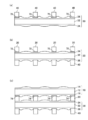
- FIG. 2 is a diagram for schematically explaining a method for manufacturing the wafer lens laminate of FIG. 1, and specifically for explaining the method for manufacturing the wafer lens of FIG. 2 in detail. It is drawing for demonstrating schematically the manufacturing method of the wafer lens laminated body of FIG. 1, Comprising: In detail, it is drawing for demonstrating schematically the process at the time of laminating
- a wafer lens laminate 1 As shown in FIG. 1, a wafer lens laminate 1 according to a preferred embodiment of the present invention has two wafer lenses 10 and 30 and two spacers 20 and 40, and these are laminated together. have. A spacer 20 is disposed between the wafer lenses 10 and 30, and a spacer 40 is disposed below the wafer lens 30.
- the wafer lens 10 has a glass substrate 12 having a disk shape.
- a resin portion 14 is formed on the upper portion of the glass substrate 12, and a resin portion 16 is formed on the lower portion of the glass substrate 12.
- the resin parts 14 and 16 are made of a photocurable resin.
- the photocurable resin any known photocurable resin can be used.
- an acrylic resin, an allyl ester resin, an epoxy resin, or the like can be used.
- the resin part 14 is formed with a plurality of lens parts 14a.
- the lens part 14a protrudes in a substantially hemispherical shape, and constitutes a convex optical surface.
- the resin portion 16 is formed with a plurality of lens portions 16a.
- the lens portion 16a is recessed in a substantially hemispherical shape, and constitutes a concave optical surface.
- the lens portion 14a and the lens portion 16a are formed at positions facing each other, and the optical axes of the lens portion 14a and the lens portion 16a coincide with the optical surface.
- the lens portions 14a and 16a are formed in the region A within the range of the optically effective surface.
- a region adjacent to the region A is a region B outside the range of the optical effective surface, and the non-lens portions 14b and 16b are formed in the region B.
- the non-lens portion 14b has a planar shape, and the non-lens portion 16b has an uneven shape.
- the wafer lens 30 has substantially the same configuration as the wafer lens 10. However, in the wafer lenses 10 and 30, if the resin portion 14 is the first layer, the resin portion 16 is the second layer, the resin portion 34 is the third layer, and the resin portion 36 is the fourth layer, one or two types are included in each layer. Infrared absorbers are added, and the absorption regions of the respective infrared absorbers in the wavelength region of 650 to 1100 nm are different from each other. The “type” of the infrared absorber indicates the difference in the absorption region. If the absorption region is the same even if the composition is different, the type of the infrared absorber is the same.
- phthalocyanine-based, cyanine-based, polymethine-based, azulenium-based, pyrylium-based, merocyanine-based, croconium-based, squalium-based, naphthoquinone-based dyes, and the like can be used.
- phthalocyanine dyes have absorptivity in the wavelength region of 600 to 700 nm.
- Cyanine dyes have been proposed as dyes used for CD-R and the like that can be recorded only once on an optical recording medium containing an organic dye. In general, substances are easily changed by light and heat. .
- an aminium salt, a diimonium salt or the like may be added to the cyanine dye as described in JP-B-6-26028, JP-A-1-99885 and the like.
- an aminium salt or a diimonium salt When an aminium salt or a diimonium salt is added, it has absorptivity in a wavelength region of 900 nm or more.
- Cyanine, polymethine, azulene, and pyrylium dyes are not heat resistant. Therefore, in order to prevent thermal oxidative degradation and improve heat resistance, these dyes may be added with antioxidants such as hindered phenol compounds, arylamine compounds, thioether compounds, phosphite compounds, etc. Good.
- the infrared absorber pigment-based near infrared absorber
- the near infrared absorber is added to 100 parts by mass of the acrylic resin.
- an average light transmittance at a wavelength of 800 nm to 1000 nm is preferably 30% or less.
- this dye-based near infrared absorber (1) Aminium-based near-infrared absorbers as disclosed in JP-A-4-174402, 160037, etc. (2) JP-A-61-115958, JP-A-61-291651, Anthraquinone near-infrared absorbers as shown in JP-A-62-132963, JP-A-1-172458, etc. (3) JP-A-2-138382, JP-A-3-62878, Phthalocyanines and naphthalocyanine-based near infrared absorbers as disclosed in JP-A-5-163440, JP-A-6-214113, etc. (4) JP-A-61-277903, JP-A-61-1 No.
- Dithiol complex-based near-infrared absorbers as described above (5) Besides these, polymethine-based absorbers, pyrylium-based absorbers, thiopyrylium-based absorbers, squarylium-based absorbers, croconium-based absorbers, azurenium-based absorbers Agents, tetradehydrocholine absorbents, triphenylmethane absorbents, diimmonium absorbents, and the like. Two or more of the above dye-based near infrared absorbers may be used in combination.
- the spacer 20 is made of a light transmissive material (glass or resin). As shown in FIG. 1B, the spacer 20 is formed with a circular transmission hole 22 at a position corresponding to the lens portion 16 a and the lens portion 34 a, and the light transmitted through the wafer lens 10 is shielded by the spacer 20. Without being incident on the wafer lens 30.
- the spacer 40 is the same member as the spacer 20.
- the resin 14A in a monomer state (before curing) is placed on the surface of the glass substrate 10 (dropping, coating, etc.), and the molding die 50 is pressed from above, and the resin is put into the cavity 52.
- One or two infrared absorbers are added to the resin 14A before filling. Thereafter, light is irradiated from above with the resin 14 ⁇ / b> A filled in the cavity 52.
- a mold having optical transparency is used as the mold 50.
- the irradiated light is transmitted through the mold 50 and incident on the resin 14A, the resin 14A is cured, and the resin portion 14 (particularly, a plurality of lens portions 14a) is formed on the glass substrate 12.
- the resin portion 14 is released from the mold 50 together with the glass substrate 12 and turned over to form the resin portion 16 on the back surface of the glass substrate 10.
- the mold 60 in FIG. 3B may be used instead of the mold 50 in FIG. 3A, and the resin 62A is irradiated with light in a state where the resin 62A is filled in the cavity 62 of the mold 60. 16A is cured to form a resin portion 16 (particularly, a plurality of lens portions 16a). Even in this case, one or two infrared absorbers are added to the resin 16A before filling.
- the resin lens 16 is released from the mold 60 together with the glass substrate 12, whereby the wafer lens 10 can be manufactured.
- wafer lens 30 may be manufactured in the same manner as the wafer lens 10 is manufactured.
- an adhesive 70 is applied to the upper surface of the resin portion 36 of the wafer lens 30 or the lower surface of the spacer 40, and the spacer 40 is placed on the wafer lens 30.
- the adhesive 70 is made of a photocurable resin and is cured by light irradiation (the same applies to the adhesives 72 and 74 described later). Thereafter, light is irradiated from above the spacer 40 to cure the adhesive 70, and the spacer 40 is fixed to the wafer lens 30.
- the spacer 20 is fixed to the resin portion 34 of the wafer lens 30 as shown in FIG.
- an adhesive 74 is applied to the lower surface of the resin portion 16 of the wafer lens 10 or the upper surface of the spacer 20, and the wafer lens 10 is placed on the spacer 20. Thereafter, light is irradiated from above the wafer lens 10 to cure the adhesive 74, and the wafer lens 10 is fixed to the spacer 20.
- the wafer lens laminate 1 can be manufactured by the above processing.
- the wafer lens stack 1 includes an image sensor (CCD (Charge Coupled Device) type image sensor or a CMOS (Complementary Metal-Oxide Semiconductor) type image sensor that receives light transmitted through the lens portions 14a, 16a, 34a, and 36a. It is suitably used as an image pickup apparatus using a solid-state image pickup device).
- the wafer lens laminate 1 is cut for each of the lens portions 14a, 16a, 34a, and 36a, and the cut piece 80 becomes a wafer lens laminate and is imaged through the spacer 40. It is incorporated on the element and used as an imaging device.
- the wafer lens 10 itself can also be used as an imaging lens.
- the wafer lens 10 is cut for each of the lens portions 14a and 16a, and the cut pieces are cut. 90 becomes a wafer lens and is incorporated on the image sensor in the same manner as described above and used as an image pickup apparatus.
- the wafer lens laminate 1 before cutting and the wafer lens laminate 1 after cutting are examples of an imaging lens unit.
- the wafer lens 10 before cutting and the wafer lens 10 after cutting (cut piece) 90) is also an example of an imaging lens.
- the imaging device including the cut piece 80 (or the cut piece 90) is preliminarily made of a conductive material such as solder. It is placed together with other electronic components at a predetermined mounting position on the coated (potted) circuit board. Thereafter, the circuit board on which the imaging device and other electronic components are placed is transferred to a reflow furnace (not shown) by a belt conveyor or the like, and the circuit board is heated at a temperature of about 260 ° C. for about 5 to 10 minutes ( Reflow processing).
- all of the infrared absorbers added to the resin parts 14, 16, 34, and 36 have a melting point of 260 ° C. or higher, and can be used for reflow treatment after molding (no alteration or the like). ).
- the conductive material is melted and the imaging device is mounted on the circuit board together with other electronic components.
- the absorption region is expanded by the number of types of the added infrared absorber, and infrared rays can be blocked or reduced over a wide region having a wavelength of 650 to 1100 nm.
- the addition of one or two kinds of infrared absorbers is allowed for each resin part 14, 16, 34, 36, and three or more kinds of infrared absorbers are not added to one resin part (layer).
- infrared absorbers it is possible to suppress the precipitation of infrared absorbers and the occurrence of bleed-out, and it is possible to prevent deterioration in optical performance such as a drop in contrast due to shadows, ghosts, and image blurring on the image sensor.
- infrared absorbers one or two types of infrared absorbers are shared and contained in each resin portion, and the effect is exhibited.
- the resin part 14, 16, 34, 36 should just form at least 2 layer among these, For example, only the resin portions 14 and 34 may be formed.
- the number of types of infrared absorbers to be added is two types at least in the resin portions 14, 16, 34, 36 from the minimum two types in the case where one type of infrared absorber is added to the resin portions 14, 34. A maximum of eight types when an infrared absorber is added is allowed.
- the wafer lens 10 and 30 are laminated in two stages, but the wafer lens 10 is laminated on the wafer lens 10 in the same manner as the wafer lens 10 is laminated on the wafer lens 30 via the spacer 20. Further, a wafer lens may be further laminated through the two, and three or more wafer lenses may be laminated as a whole. Also in this case, the resin part should just be formed in two or more layers, and the number of types of infrared absorbers to be added is from a minimum of two types in the case where one type of infrared absorber is added to each of the two-layer resin parts. A maximum of 4n types when two types of infrared absorbers are added to the resin portion of the 2n (n: the number of laminated wafer lenses is 3 or more) layers is allowed.
- Samples 11 types of wafer lens laminates (two wafer lens laminates) similar to those shown in FIG. 1 were produced, and processing described later (addition of infrared absorber, infrared light shielding film) for each wafer lens laminate.
- Samples 1 to 11 were formed.
- Epoxy resins (4% by mass of UVI-6992 as a UV curing initiator added to hydrogenated bisphenol A type epoxy resin) were used for the production of the lens portions of Samples 1 to 11.
- an infrared absorber (dye 1 to 6) was added to the epoxy resin as shown in Table 1, and the resin was molded on a glass substrate to form a lens portion. The amount of each dye added to the resin is also shown.
- Dye 1 Absorptive dye ABS670T (absorption maximum 670 nm), full width at half maximum 655 to 680 nm, manufactured by Exciton Inc. Addition amount 0.2% by mass (based on resin) Pigment 2: Yamada Chemical Co., Ltd. Phthalocyanine dye (absorption maximum near 710 nm) Half width 680 to 740 nm Addition amount 2% by mass (based on resin)
- Dye 3 Near-infrared absorbing dye IR-406 manufactured by Yamada Chemical Co., Ltd.
- Dye 4 Absorptive dye IRA868 (absorption maximum 868 nm), full width at half maximum 800 to 910 nm, manufactured by Exciton, Inc. 2 mass% (based on resin)
- Dye 5 Absorption dye IRA908 (absorption maximum 908 nm) manufactured by Exciton, Inc.
- Half-width 880 to 980 nm Addition amount 1% by mass (based on resin)
- Dye 6 Absorption dye IRA1034 (absorption maximum 1034 nm) manufactured by Exciton, Inc.
- an antireflection film (AR coating) was formed on the surface of the lens portion by vacuum deposition.
- the wafer lens was mounted in a vacuum deposition apparatus, the pressure in the apparatus was reduced to 2 ⁇ 10 ⁇ 3 Pa, and the wafer lens was heated to a temperature of 240 ° C. by a heater at the top of the apparatus.
- OA600 manufactured by Optron Co. was used as a film raw material and evaporated by electron gun heating to form a Ta 2 O 5 + 5% TiO 2 film (film thickness 20 nm) on the wafer lens (lens portion).
- Average light transmittance transmittance ⁇ (incident side surface reflectance + outgoing side surface reflectance) (A) Table 1 shows the calculation results of the average light transmittance.
- the criteria for ⁇ and ⁇ are as follows.
- Sample 4 in which one type of dye 1, 3, 5, and 6 was added to each layer of the resin portion had a slightly low IR cut effect, but Samples 1 and 4 in which one or two kinds of dyes were added to each layer. In ⁇ 8, there was no problem of precipitation and bleed-out, and a desired effect was obtained as an IR cut effect. From the above, the addition of one or two infrared absorbers having different absorption regions to each layer of the resin portion can block or reduce infrared rays over a wide region of wavelength 650 to 1100 nm, and It turns out that it is useful in suppressing the occurrence of precipitation and bleed-out.
Landscapes
- Physics & Mathematics (AREA)
- General Physics & Mathematics (AREA)
- Optics & Photonics (AREA)
- Optical Filters (AREA)
Abstract
L'invention porte sur une unité de lentille d'imagerie qui bloque ou réduit la lumière infrarouge sur une large région à une longueur d'onde comprise entre 650 et 1 100 nm et supprime le dépôt et l'exsudation d'un absorbant de lumière infrarouge. Dans un corps stratifié de lentille mince (1), à savoir, un exemple des unités de lentille d'imagerie de cette invention, des lentilles minces (10, 30) dans lesquelles des sections de résine (14, 16, 34, 36) composées d'une résine photodurcissable sont formées sur des substrats en verre (12, 32) sont stratifiées en deux couches ou plus, un ou deux types d'absorbants de lumière infrarouge sont ajoutés aux sections de résine (14, 16, 34, 36) et les régions absorbantes des absorbants de lumière infrarouge respectifs sont différentes les unes des autres.
Applications Claiming Priority (2)
| Application Number | Priority Date | Filing Date | Title |
|---|---|---|---|
| JP2008-282008 | 2008-10-31 | ||
| JP2008282008 | 2008-10-31 |
Publications (1)
| Publication Number | Publication Date |
|---|---|
| WO2010050297A1 true WO2010050297A1 (fr) | 2010-05-06 |
Family
ID=42128665
Family Applications (1)
| Application Number | Title | Priority Date | Filing Date |
|---|---|---|---|
| PCT/JP2009/065489 WO2010050297A1 (fr) | 2008-10-31 | 2009-09-04 | Lentille d'imagerie, unité de lentille d'imagerie et dispositif d'imagerie |
Country Status (1)
| Country | Link |
|---|---|
| WO (1) | WO2010050297A1 (fr) |
Cited By (1)
| Publication number | Priority date | Publication date | Assignee | Title |
|---|---|---|---|---|
| EP3318920A1 (fr) * | 2016-11-04 | 2018-05-09 | Essilor International | Articles optiques coupant la lumière proche infrarouge à faible couleur résiduelle |
Citations (9)
| Publication number | Priority date | Publication date | Assignee | Title |
|---|---|---|---|---|
| JPS61115958A (ja) * | 1984-11-09 | 1986-06-03 | Mitsubishi Chem Ind Ltd | アントラキノン誘導体 |
| JPS63139303A (ja) * | 1986-08-05 | 1988-06-11 | Fuji Photo Film Co Ltd | 赤外線吸収性組成物 |
| JP2004200360A (ja) * | 2002-12-18 | 2004-07-15 | Toppan Printing Co Ltd | 固体撮像素子及びその製造方法 |
| WO2006003807A1 (fr) * | 2004-06-30 | 2006-01-12 | Toppan Printing Co., Ltd. | Élément de traitement de l’image |
| JP2006106229A (ja) * | 2004-10-04 | 2006-04-20 | Nippon Sheet Glass Co Ltd | 透過型光学素子の製造方法および透過型光学素子 |
| JP2006278356A (ja) * | 2005-03-25 | 2006-10-12 | Dainippon Printing Co Ltd | 固体撮像素子の製造方法及び固体撮像素子 |
| JP3926380B1 (ja) * | 2006-12-07 | 2007-06-06 | マイルストーン株式会社 | 撮像レンズ |
| JP2007221231A (ja) * | 2006-02-14 | 2007-08-30 | Denso Corp | 撮像モジュールおよびその製造方法 |
| JP2007242771A (ja) * | 2006-03-07 | 2007-09-20 | Toppan Printing Co Ltd | 撮像素子の製造方法及び撮像素子 |
-
2009
- 2009-09-04 WO PCT/JP2009/065489 patent/WO2010050297A1/fr active Application Filing
Patent Citations (9)
| Publication number | Priority date | Publication date | Assignee | Title |
|---|---|---|---|---|
| JPS61115958A (ja) * | 1984-11-09 | 1986-06-03 | Mitsubishi Chem Ind Ltd | アントラキノン誘導体 |
| JPS63139303A (ja) * | 1986-08-05 | 1988-06-11 | Fuji Photo Film Co Ltd | 赤外線吸収性組成物 |
| JP2004200360A (ja) * | 2002-12-18 | 2004-07-15 | Toppan Printing Co Ltd | 固体撮像素子及びその製造方法 |
| WO2006003807A1 (fr) * | 2004-06-30 | 2006-01-12 | Toppan Printing Co., Ltd. | Élément de traitement de l’image |
| JP2006106229A (ja) * | 2004-10-04 | 2006-04-20 | Nippon Sheet Glass Co Ltd | 透過型光学素子の製造方法および透過型光学素子 |
| JP2006278356A (ja) * | 2005-03-25 | 2006-10-12 | Dainippon Printing Co Ltd | 固体撮像素子の製造方法及び固体撮像素子 |
| JP2007221231A (ja) * | 2006-02-14 | 2007-08-30 | Denso Corp | 撮像モジュールおよびその製造方法 |
| JP2007242771A (ja) * | 2006-03-07 | 2007-09-20 | Toppan Printing Co Ltd | 撮像素子の製造方法及び撮像素子 |
| JP3926380B1 (ja) * | 2006-12-07 | 2007-06-06 | マイルストーン株式会社 | 撮像レンズ |
Cited By (3)
| Publication number | Priority date | Publication date | Assignee | Title |
|---|---|---|---|---|
| EP3318920A1 (fr) * | 2016-11-04 | 2018-05-09 | Essilor International | Articles optiques coupant la lumière proche infrarouge à faible couleur résiduelle |
| WO2018082946A1 (fr) * | 2016-11-04 | 2018-05-11 | Essilor International | Articles optiques de coupe de lumière proche infrarouge à faible couleur résiduelle |
| US11124599B2 (en) | 2016-11-04 | 2021-09-21 | Essilor International | Near infrared light-cutting optical articles with low residual color |
Similar Documents
| Publication | Publication Date | Title |
|---|---|---|
| KR101876229B1 (ko) | 근-적외선 흡수 필터 및 이미지 센서 | |
| JP6087464B1 (ja) | 赤外線カットフィルタ及び撮像光学系 | |
| JP7326993B2 (ja) | 光学フィルター、その製造方法およびその用途 | |
| JP7251423B2 (ja) | 光学部材及びカメラモジュール | |
| JP5823119B2 (ja) | 紫外赤外線カット用光学フィルタ | |
| KR20170074911A (ko) | 카메라 모듈용 광학 장치, 광학 장치를 지닌 카메라 모듈 및 광학 장치의 제조 방법 | |
| JP6642575B2 (ja) | 光学フィルタおよび近赤外線カットフィルタ | |
| JP5759717B2 (ja) | 監視カメラ用撮像光学系 | |
| TWI753299B (zh) | 光學濾波器及其用途 | |
| TW201415091A (zh) | 紅外線截止濾光片及攝影裝置 | |
| EP3480633B1 (fr) | Filtre optique, module de caméra et dispositif électronique le comprenant | |
| JP2012137649A (ja) | 光学フィルタ | |
| CN108700688A (zh) | 玻璃盖板的层叠结构、照相机结构、成像装置 | |
| JP2012137651A (ja) | 光学フィルタ | |
| JP2020109496A (ja) | 光学フィルタおよび近赤外線カットフィルタ | |
| CN110073247A (zh) | 光学元件、成像元件封装、成像装置和电子设备 | |
| JP2021009271A (ja) | カメラモジュールおよび電子機器 | |
| KR101866104B1 (ko) | 카메라 모듈에 포함되는 근적외선 컷-오프 필터용 광학물품 및 이를 포함하는 카메라 모듈용 근적외선 컷-오프 필터 | |
| JP7143881B2 (ja) | 光学フィルターおよびその用途 | |
| WO2010050297A1 (fr) | Lentille d'imagerie, unité de lentille d'imagerie et dispositif d'imagerie | |
| JP6955343B2 (ja) | 赤外線カットフィルタ及び撮像光学系 | |
| JP2018180430A (ja) | 光学フィルタ | |
| JP2024041789A (ja) | 光学フィルタ、近赤外線カットフィルタ、および撮像装置 | |
| JP2023043847A (ja) | 光学部材 | |
| JP6706700B2 (ja) | 赤外線カットフィルタ、撮像装置および赤外線カットフィルタの製造方法 |
Legal Events
| Date | Code | Title | Description |
|---|---|---|---|
| 121 | Ep: the epo has been informed by wipo that ep was designated in this application |
Ref document number: 09823410 Country of ref document: EP Kind code of ref document: A1 |
|
| NENP | Non-entry into the national phase |
Ref country code: DE |
|
| 122 | Ep: pct application non-entry in european phase |
Ref document number: 09823410 Country of ref document: EP Kind code of ref document: A1 |
|
| NENP | Non-entry into the national phase |
Ref country code: JP |