WO2009144951A1 - Light-receiving device and production therof - Google Patents
Light-receiving device and production therof Download PDFInfo
- Publication number
- WO2009144951A1 WO2009144951A1 PCT/JP2009/002382 JP2009002382W WO2009144951A1 WO 2009144951 A1 WO2009144951 A1 WO 2009144951A1 JP 2009002382 W JP2009002382 W JP 2009002382W WO 2009144951 A1 WO2009144951 A1 WO 2009144951A1
- Authority
- WO
- WIPO (PCT)
- Prior art keywords
- light receiving
- resin
- frame member
- base substrate
- receiving device
- Prior art date
- Legal status (The legal status is an assumption and is not a legal conclusion. Google has not performed a legal analysis and makes no representation as to the accuracy of the status listed.)
- Ceased
Links
Images


Classifications
-
- H—ELECTRICITY
- H10—SEMICONDUCTOR DEVICES; ELECTRIC SOLID-STATE DEVICES NOT OTHERWISE PROVIDED FOR
- H10F—INORGANIC SEMICONDUCTOR DEVICES SENSITIVE TO INFRARED RADIATION, LIGHT, ELECTROMAGNETIC RADIATION OF SHORTER WAVELENGTH OR CORPUSCULAR RADIATION
- H10F77/00—Constructional details of devices covered by this subclass
- H10F77/50—Encapsulations or containers
-
- C—CHEMISTRY; METALLURGY
- C09—DYES; PAINTS; POLISHES; NATURAL RESINS; ADHESIVES; COMPOSITIONS NOT OTHERWISE PROVIDED FOR; APPLICATIONS OF MATERIALS NOT OTHERWISE PROVIDED FOR
- C09J—ADHESIVES; NON-MECHANICAL ASPECTS OF ADHESIVE PROCESSES IN GENERAL; ADHESIVE PROCESSES NOT PROVIDED FOR ELSEWHERE; USE OF MATERIALS AS ADHESIVES
- C09J163/00—Adhesives based on epoxy resins; Adhesives based on derivatives of epoxy resins
-
- C—CHEMISTRY; METALLURGY
- C08—ORGANIC MACROMOLECULAR COMPOUNDS; THEIR PREPARATION OR CHEMICAL WORKING-UP; COMPOSITIONS BASED THEREON
- C08L—COMPOSITIONS OF MACROMOLECULAR COMPOUNDS
- C08L2666/00—Composition of polymers characterized by a further compound in the blend, being organic macromolecular compounds, natural resins, waxes or and bituminous materials, non-macromolecular organic substances, inorganic substances or characterized by their function in the composition
- C08L2666/02—Organic macromolecular compounds, natural resins, waxes or and bituminous materials
- C08L2666/14—Macromolecular compounds according to C08L59/00 - C08L87/00; Derivatives thereof
- C08L2666/22—Macromolecular compounds not provided for in C08L2666/16 - C08L2666/20
-
- C—CHEMISTRY; METALLURGY
- C08—ORGANIC MACROMOLECULAR COMPOUNDS; THEIR PREPARATION OR CHEMICAL WORKING-UP; COMPOSITIONS BASED THEREON
- C08L—COMPOSITIONS OF MACROMOLECULAR COMPOUNDS
- C08L63/00—Compositions of epoxy resins; Compositions of derivatives of epoxy resins
- C08L63/10—Epoxy resins modified by unsaturated compounds
-
- H—ELECTRICITY
- H10—SEMICONDUCTOR DEVICES; ELECTRIC SOLID-STATE DEVICES NOT OTHERWISE PROVIDED FOR
- H10F—INORGANIC SEMICONDUCTOR DEVICES SENSITIVE TO INFRARED RADIATION, LIGHT, ELECTROMAGNETIC RADIATION OF SHORTER WAVELENGTH OR CORPUSCULAR RADIATION
- H10F39/00—Integrated devices, or assemblies of multiple devices, comprising at least one element covered by group H10F30/00, e.g. radiation detectors comprising photodiode arrays
- H10F39/80—Constructional details of image sensors
- H10F39/804—Containers or encapsulations
Definitions
- the present invention relates to a light receiving device and a manufacturing method thereof.
- FIG. 10 is a cross-sectional view of the base substrate 101 and the transparent substrate 102 in a direction orthogonal to the substrate surface.
- a solid-state imaging device includes a base substrate 101 on which a microlens array is formed, a transparent substrate 102, a light receiving unit 104 formed by the microlens array, and a frame member 103 formed so as to surround the light receiving unit 104. And have.
- Patent document 1 is an example.
- the frame member 103 is made of a resin composition containing a photocurable resin. Thereby, it is possible to form a pattern on the base substrate 101 and the transparent substrate 102 according to the characteristics of the photocurable resin contained in the frame member 103, and it is possible to form the frame member 103 with a high accuracy and a fine pattern.
- the decrease in the strength of the frame member is caused by an undercut generated in the frame member.
- the undercut was considered to be caused by the penetration of the developer into the frame member because the base substrate or the transparent substrate side in the frame member thickness direction was weakly cured.
- the frame member sometimes peeled off when the undercut was severe.
- the present inventors have revealed that the residue in the internal space after exposure and development contains an inorganic filler. This was presumably because the inorganic filler was detached from the frame member during development and became a foreign substance. The foreign matter adheres to the transparent substrate and the base substrate, adversely affects the imaging characteristics, and decreases the yield.
- the frame member not containing the inorganic filler reduces the shape retention ability of the hollow package after exposure.
- the present invention has been made in view of the above circumstances, and the object of the present invention is to provide a light receiving device that employs a hollow package while maintaining the shape retention ability and the content of the inorganic filler in the frame member.
- the purpose is to reduce the occurrence of foreign matter in the internal space and the undercut of the frame member by a certain amount or less.
- At least one light receiving unit At least one light receiving unit; A base substrate provided with the light receiving portion; A transparent substrate disposed opposite to the base substrate and the light receiving unit; A frame member disposed so as to surround a light receiving portion between the base substrate and the transparent substrate; With The frame member is formed by curing a resin composition,
- the resin composition is An alkali-soluble resin;
- a photopolymerizable resin 9% by weight or less of inorganic filler, Including
- the photopolymerizable resin includes an acrylic polyfunctional monomer,
- the frame member is provided with a light receiving device that satisfies the following conditions (a) and (b).
- Moisture permeability of the frame member measured by JIS Z0208 B method is 12 [g / m 2 ⁇ 24 h] or more
- the elastic modulus at 80 ° C. of the frame member after exposure to 700 mJ / cm 2 with light of a line (365 nm) is 100 Pa or more.
- an adhesive made of an electron beam curable resin composition on a base substrate provided with at least one light receiving portion or a transparent substrate so as to cover the base substrate or the transparent substrate.
- a process of attaching a film; The adhesive film is selectively irradiated with an electron beam, and at least the region surrounding the light receiving portion on the base substrate, or the transparent substrate when the transparent substrate is disposed opposite to the base substrate, the transparent substrate.
- the resin composition is An alkali-soluble resin; A photopolymerizable resin; 9% by weight or less of inorganic filler, Including The photopolymerizable resin includes an acrylic polyfunctional monomer,
- the frame member is provided with a method for manufacturing a light receiving device that satisfies the following conditions (a) and (b).
- Moisture permeability of the frame member measured by JIS Z0208 B method is 12 [g / m 2 ⁇ 24 h] or more
- the elastic modulus at 80 ° C. of the frame member after exposure to 700 mJ / cm 2 with light of a line (365 nm) is 100 Pa or more.
- produces inside a hollow package can be reduced by making an inorganic filler into 9 weight% or less with respect to the resin composition which comprises a frame member.
- the light transmittance of a frame member can be improved and hardening of a resin composition can be strengthened by making an inorganic filler into 9 weight% or less of the said resin composition. Therefore, it is possible to prevent the developer from oozing into the frame member during exposure and to prevent occurrence of undercut.
- the moisture permeability of the frame member is set to 12 [g / m 2 ⁇ 24 h] or more, and light of all wavelengths is exposed with a mercury lamp.
- the elastic modulus at 80 ° C. of the frame member after exposure so that the accumulated exposure amount is 700 mJ / cm 2 with i-line (365 nm) light can be 100 Pa or more. Therefore, the frame member of the present invention is excellent in terms of strength and moisture permeability. From the above, according to the present invention, it is possible to improve the reliability by preventing the occurrence of condensation while maintaining the shape retaining property of the light receiving device.
- the photopolymerizable resin includes an epoxy vinyl ester resin.
- the weight content of the epoxy vinyl ester resin is 3 to 30% of the resin composition.
- the acrylic polyfunctional monomer is a (meth) acrylic acid ester compound.
- the acrylic polyfunctional monomer is a trifunctional (meth) acrylate compound or a tetrafunctional (meth) acrylate compound.
- the acrylic polyfunctional monomer is trimethylolpropane tri (meth) acrylate.
- the acrylic polyfunctional monomer has a weight content of 1 to 50% of the resin composition.
- the alkali-soluble resin is a (meth) acryl-modified novolak resin.
- the weight content of the alkali-soluble resin is 50 to 95% of the resin composition.
- the various components of the present invention do not have to be individually independent, but a plurality of components are formed as a single member, and a single component is formed of a plurality of members. It may be that a certain component is a part of another component, a part of a certain component overlaps a part of another component, and the like.
- a light receiving device employing a hollow package
- shape retention and moisture permeability are improved while reducing undercut properties and residues after exposure.
- the light receiving device 1 of the present embodiment includes a plurality of light receiving portions 11, a base substrate 12A provided with the light receiving portions 11, a transparent substrate 13A disposed opposite to the base substrate 12A and the light receiving portion 11, and the base substrate 12A and the transparent substrate. And a frame member 14A disposed so as to surround the light receiving unit 11 with the substrate 13A.
- the frame member 14A is formed by curing a resin composition.
- This resin composition contains an alkali-soluble resin, a photopolymerizable resin, and 9% by weight or less of an inorganic filler.
- the photopolymerizable resin contains an acrylic polyfunctional monomer.
- the frame member 14A satisfies the following conditions (a) and (b).
- the moisture permeability of the frame member 14A measured by the JIS Z0208 B method is 12 [g / m 2 ⁇ 24h] or more.
- the elastic modulus at 80 ° C. of the frame member 14A after being exposed to 700 mJ / cm 2 with light of a line (365 nm) is 100 Pa or more.
- FIG. 1 is a cross-sectional view in a direction orthogonal to the substrate surface of the base substrate 12A and the transparent substrate 13A.
- the light receiving device 1 is used as a solid-state imaging device.
- the light receiving device 1 includes a base substrate 12A, a transparent substrate 13A, a light receiving unit 11 including a light receiving element, and a frame member 14A formed so as to surround the light receiving unit 11.
- the base substrate 12A is, for example, a semiconductor substrate, and a microlens array is formed on the base substrate 12A.
- the transparent substrate 13A is disposed so as to face the base substrate 12A and has substantially the same planar dimension as the planar dimension of the base substrate 12A.
- the transparent substrate 13A is, for example, an acrylic resin, a polyethylene terephthalate resin (PET), a glass substrate, or the like.
- the frame member 14A is directly bonded to the microlens array on the base substrate 12A and the transparent substrate 13A, and bonds the base substrate 12A and the transparent substrate 13A.
- the frame member 14A is disposed so as to surround the center portion of the microlens array of the base substrate 12A, and a portion of the microlens array surrounded by the frame member 14A functions as the light receiving unit 11.
- a photoelectric conversion unit (not shown) is formed on the lower surface of the light receiving unit 11, that is, the base substrate 12A, and light received by the light receiving unit 11 is converted into an electric signal.
- a light receiving element such as a charge coupled device (CCD) and a complementary metal oxide semiconductor (CMOS) is formed.
- an adhesive film 14 made of an electron beam curable resin composition is provided on a base substrate 12 provided with a plurality of light receiving portions 11 or a transparent substrate 13 so as to cover the base substrate 12 or the transparent substrate 13. And a step of selectively irradiating the adhesive film 14 with an electron beam and at least a region surrounding the light receiving portion 11 on the base substrate 12 or the transparent substrate 13 facing the base substrate 12.
- the transparent substrate 13 is provided between the base substrate 12 and the transparent substrate 13 and is formed of an adhesive film 14 so as to surround the light receiving unit 11. And a step of obtaining a light receiving device having a frame member 14A which is.
- the electron beam is a concept including radiation having a wavelength of 150 nm to 700 nm, and includes, for example, near ultraviolet rays and ultraviolet rays.
- a base substrate 12 provided with a plurality of light receiving portions 11 is prepared. That is, a microlens array is formed on the base substrate 12. In addition, a light receiving element is formed at a location to be the light receiving unit 11.
- an adhesive film 14 is attached so as to cover the surface of the base substrate 12 (the surface on which the light receiving portion 11 is provided).
- the adhesive film 14 is composed of a resin composition containing an alkali-soluble resin and a photopolymerizable resin.
- the adhesive film 14 preferably has a moisture permeability measured by the JIS Z0208 B method of 12 [g / m 2 ⁇ 24 h] or more, particularly preferably 14 to 100 [g / m 2 ⁇ 24 h]. If it is less than the lower limit, condensation on the transparent substrate 13A or the like of the light receiving device 1 may not be sufficiently prevented. When the upper limit is exceeded, the moisture absorption reflow reliability of the adhesive film 14 may be lowered.
- the moisture permeability can be evaluated at 40 ° C./90% according to the moisture permeable cup method (JIS Z0208 B method) using the adhesive film 14 having a thickness of 100 ⁇ m.
- the adhesive film 14 is exposed to light of all wavelengths with a mercury lamp, and has an elastic modulus at 80 ° C. of 100 Pa or more after exposure so that the accumulated exposure amount is 700 mJ / cm 2 with i-line (365 nm) light. In particular, 500 to 30000 Pa is preferable. If it is less than the lower limit, the shape retainability when the base substrate and the transparent substrate are attached is lowered. When the upper limit is exceeded, it becomes difficult to attach the base substrate and the transparent substrate after patterning.
- alkali-soluble resin examples include (meth) acryl-modified novolak resin such as (meth) acryl-modified bis A novolak resin, acrylic resin, copolymer of styrene and acrylic acid, polymer of hydroxystyrene, polyvinylphenol, poly Examples include ⁇ -methylvinylphenol, among which alkali-soluble novolak resins are preferable, and (meth) acryl-modified novolak resins are particularly preferable.
- novolak resin such as (meth) acryl-modified bis A novolak resin, acrylic resin, copolymer of styrene and acrylic acid, polymer of hydroxystyrene, polyvinylphenol, poly Examples include ⁇ -methylvinylphenol, among which alkali-soluble novolak resins are preferable, and (meth) acryl-modified novolak resins are particularly preferable.
- the content of the alkali-soluble resin is not particularly limited, but 50 to 95% by weight of the resin composition constituting the adhesive film 14 is preferable. When the content is less than the lower limit, curing for improving the compatibility may be reduced, and developability or resolution exceeding the upper limit may be reduced.
- An acrylic polyfunctional monomer is used as the photopolymerizable resin.
- a polyfunctional monomer refers to a monomer having three or more functions, and in the present embodiment, a trifunctional or tetrafunctional acrylate compound can be suitably used.
- Monofunctional or lower monomers are not preferable because the strength of the frame member 14A is weak and the shape of the light receiving device 1 cannot be maintained.
- trifunctional (meth) acrylates such as trimethylolpropane tri (meth) acrylate and pentaerythritol tri (meth) acrylate, pentaerythritol tetra (meth) acrylate, and ditrimethylolpropane
- tetrafunctional (meth) acrylates such as tetra (meth) acrylate and hexafunctional (meth) acrylates such as dipentaerythritol hexa (meth) acrylate.
- trifunctional (meth) acrylate or tetrafunctional (meth) acrylate is preferable.
- the content of the acrylic polyfunctional monomer is not particularly limited, but is preferably 1 to 50% by weight, particularly preferably 5 to 25% by weight of the resin composition constituting the adhesive film 14.
- the strength of the frame member when the base substrate and the transparent substrate are attached is lowered.
- the upper limit is exceeded, the sticking property between the base substrate and the transparent substrate may be lowered.
- the photopolymerizable resin may contain an epoxy vinyl ester resin.
- an epoxy vinyl ester resin since it radical-polymerizes with a polyfunctional monomer at the time of exposure, the intensity
- the solubility in an alkaline developer is improved, so that residues after development can be reduced.
- Epoxy vinyl ester resins include 2-hydroxy-3-phenoxypropyl acrylate, Epolite 40E methacrylic adduct, Epolite 70P acrylic acid adduct, Epolite 200P acrylic acid adduct, Epolite 80MF acrylic acid adduct, Epolite 3002 methacrylic acid adduct.
- the content of the epoxy vinyl ester resin is not particularly limited, but is preferably 3 to 30% by weight of the resin composition constituting the adhesive film 14.
- the upper limit is exceeded, the water absorption characteristics of the frame member are lowered, and condensation tends to occur. If it is less than the lower limit, the solubility of the frame member in an alkaline developer may be insufficient, and a residue may be generated after development.
- the content is preferably in the range of 5 to 15% by weight. By doing so, it becomes possible to further reduce foreign matters remaining on the surfaces of the base substrate 12A and the transparent substrate 13A after being attached.
- the adhesive film 14 preferably contains a photopolymerization initiator. Thereby, the adhesive film 14 can be efficiently patterned by photopolymerization.
- photopolymerization initiator examples include benzophenone, acetophenone, benzoin, benzoin isobutyl ether, methyl benzoin benzoate, benzoin benzoic acid, benzoin methyl ether, benzylfinyl sulfide, benzyl, dibenzyl, and diacetyl.
- the content of the photopolymerization initiator is not particularly limited, but is preferably 0.5 to 5% by weight, particularly preferably 0.8 to 3.0% by weight, based on the entire resin composition. If the content is less than the lower limit, the effect of initiating photopolymerization may be reduced, and if the content exceeds the upper limit, the reactivity may be too high and storage stability and resolution may be reduced.
- the adhesive film 14 preferably contains a thermosetting resin. Thereby, it can have adhesiveness even after exposing, developing and patterning the adhesive film. That is, the base substrate 12A and the transparent substrate 13A can be joined by thermocompression bonding after the adhesive film is joined and exposed, developed, and patterned to place the adhesive component at a predetermined position.
- thermosetting resins examples include phenol novolac resins, cresol novolac resins, novolac phenol resins such as bisphenol A novolac resins, phenol resins such as resol phenol resins, bisphenol epoxy resins such as bisphenol A epoxy resins and bisphenol F epoxy resins.
- Novolac epoxy resins cresol novolac epoxy resins, novolac epoxy resins, biphenyl type epoxy resins, stilbene type epoxy resins, triphenolmethane type epoxy resins, alkyl-modified triphenolmethane type epoxy resins, triazine nucleus-containing epoxy resins, dicyclo Epoxy resins such as pentadiene-modified phenolic epoxy resins, urea (urea) resins, resins having a triazine ring such as melamine resins, unsaturated polymers Ester resins, bismaleimide resins, polyurethane resins, diallyl phthalate resins, silicone resins, resins having a benzoxazine ring, cyanate ester resins, epoxy-modified siloxane and the like, which may be used individually or as a mixture.
- an epoxy resin is particularly preferable. Thereby, heat resistance and adhesiveness can be improved more.
- an epoxy resin that is solid at room temperature particularly a bisphenol type epoxy resin
- an epoxy resin that is liquid at room temperature particularly a silicone-modified epoxy resin that is liquid at room temperature
- the content of the thermosetting resin is not particularly limited, but is preferably 10 to 40% by weight, particularly preferably 15 to 35% by weight, based on the entire resin composition constituting the adhesive film 14. If the content is less than the lower limit, the effect of improving heat resistance may be reduced, and if the content exceeds the upper limit, the effect of improving the toughness of the adhesive film 14 may be reduced.
- thermosetting resin may further include a phenol novolac resin.
- the developability can be improved by adding a phenol resin.
- thermosetting property of the epoxy resin can be improved, and the strength of the frame member 14A can be further improved.
- the adhesive film 14 may contain an inorganic filler, it is 9 wt% or less of the entire resin composition constituting the adhesive film 14. Exceeding the upper limit is not preferable because foreign substances due to the inorganic filler adhere to the substrate or undercut occurs. In this embodiment, the inorganic filler may not be included.
- inorganic fillers include fibrous fillers such as alumina fibers and glass fibers, acicular fillers such as potassium titanate, wollastonite, aluminum borate, acicular magnesium hydroxide, and whiskers, talc, mica, and sericite. , Glass flakes, flake graphite, plate-like fillers such as plate-like calcium carbonate, spherical fillers such as calcium carbonate, silica, fused silica, fired clay and unfired clay, porous fillings such as zeolite and silica gel Materials and the like. These may be used alone or in combination of two or more. Among these, a porous filler is preferable.
- the average particle diameter of the inorganic filler is not particularly limited, but is preferably 0.01 to 90 ⁇ m, and particularly preferably 0.1 to 40 ⁇ m. If the average particle diameter exceeds the upper limit, there may be abnormal appearance of the film or poor resolution, and if it is less than the lower limit, it may result in poor adhesion during heat pasting.
- the average particle diameter can be evaluated using, for example, a laser diffraction particle size distribution analyzer SALD-7000 (manufactured by Shimadzu Corporation).
- the inorganic filler a porous filler may be used as the inorganic filler.
- the average pore diameter of the porous filler is preferably 0.1 to 5 nm, particularly preferably 0.3 to 1 nm. If the average pore diameter exceeds the upper limit value, a part of the resin component may enter the pores and the reaction may be hindered. If the average pore diameter is less than the lower limit value, the water absorption ability is reduced. The rate may decrease.
- the resin composition constituting the adhesive film 14 contains additives such as a plastic resin, a leveling agent, an antifoaming agent, and a coupling agent in addition to the above-described curable resin and filler as long as the object of the present invention is not impaired. can do.
- the adhesive film 14 is selectively irradiated with an electron beam (for example, ultraviolet rays). Thereby, the part irradiated with light among the adhesive films 14 is photocured.
- an electron beam for example, ultraviolet rays
- the exposed adhesive film 14 is developed with a developer (for example, an alkaline aqueous solution, an organic solvent, etc.)
- the light irradiated portion remains without being dissolved in the developer.
- the adhesive film 14 is left in a region other than the light receiving portions 11 on the base substrate 12 so as to surround the light receiving portions 11 (see FIG. 2C). Specifically, as shown in the plan view of FIG. 3, the adhesive film 14 is left in a lattice shape.
- the transparent substrate 13 is placed on the adhesive film 14, and the base substrate 12 and the transparent substrate 13 are bonded by the adhesive film 14.
- the base substrate 12 and the transparent substrate 13 are pressed or heated and pressed, and bonded via the adhesive film 14.
- the bonded base substrate 12 and transparent substrate 13 are divided according to the light receiving unit (see FIG. 2D). Specifically, first, while supplying water to the base substrate 12, the base substrate 12 is cut with a dicing saw to form the grooves 12B. Next, a metal film (not shown) is formed by sputtering or the like so as to cover the side surface of the groove 12B and the bottom surface of the base substrate 12.
- a cut is made with a dicing saw from the transparent substrate 13 side, and the base substrate 12 and the transparent substrate 13 are divided according to the light receiving unit 11 unit. Also at this time, dicing is performed while supplying water to the base substrate 12, the transparent substrate 13, and the adhesive film 14.
- the adhesive film 14 after the exposure remains in a region other than the light receiving portion 11, when the base substrate 12 and the transparent substrate 13 are divided according to the light receiving portion unit, the adhesive film 14 is also included. Dicing will be performed.
- the light receiving device 1 obtained by the above steps is mounted on a support substrate (not shown) via solder bumps, for example. Wiring is patterned on the support substrate, and this wiring and a metal film (not shown) on the bottom surface of the base substrate 12 of the light receiving device 1 are electrically connected via solder bumps.
- produces in the inside of a hollow package can be reduced by making an inorganic filler into 9 weight% or less of a resin composition.
- the inorganic filler by setting the inorganic filler to 9% by weight or less of the resin composition, the light transmittance of the frame member 14A can be improved, and the post-exposure curing of the resin composition can be enhanced. Therefore, it is possible to prevent the developer from oozing into the frame member 14A during development, thereby preventing the occurrence of undercut.
- the moisture permeability of the frame member measured by the JIS Z0208 B method is set to 12 [g / m 2 by using a photopolymerizable resin containing an alkali-soluble resin and an acrylic polyfunctional monomer. 24 h] or higher, and exposure to light of all wavelengths with a mercury lamp, and 80 ° C. of the frame member after exposure so that the integrated exposure amount is 700 mJ / cm 2 with i-line (365 nm) light.
- the elastic modulus in can be 100 Pa or more. Therefore, the frame member 14A is excellent in terms of strength and moisture permeability. From the above, according to the present embodiment, it is possible to improve the reliability by preventing the occurrence of condensation while maintaining the shape retaining property of the light receiving device 1.
- the strength of the frame member was maintained by including an inorganic filler in the adhesive film.
- an acrylic polyfunctional monomer is used as the photopolymerizable resin. Therefore, the crosslinking density can be improved by curing by light irradiation, and the strength of the frame member can be increased. Therefore, it is possible to maintain the strength of the frame member without using an inorganic filler.
- an inorganic filler is 9 weight% or less of a resin composition
- produces in internal space can be reduced.
- foreign substances adhering to the base substrate 12A and the transparent substrate 13A can be reduced, and adverse effects on the light receiving elements of the light receiving unit 11 can be reduced.
- the inorganic filler is 9% by weight or less of the resin composition
- the light transmittance of the adhesive film 14 can be improved. Therefore, the curing of the resin composition is enhanced, the strength of the frame member 14A is improved, and the penetration of the developer during exposure is reduced. Therefore, it is possible to reduce the undercut generated in the frame member 14A.
- the adhesive film 14 is also diced.
- the present invention is not limited thereto, and the adhesive film 14 is diced. You don't have to.
- the base substrate 12 and the transparent substrate 13 may be diced at a two-dot chain line A.
- the distance between the end portion of the base substrate 12A and the outer peripheral portion of the frame portion 14A is 20% or less of the width dimension of the frame portion 14A. To do. Thereby, size reduction of a light-receiving device can be achieved.
- the adhesive film 14 (frame member 14A) and the base substrate 12 (base substrate 12A) were adhere
- the adhesive film 14 (frame member 14A) ) And the base substrate 12 (base substrate 12A) may be in direct contact with each other.
- the microlenses are formed on the entire surface of the base substrate 12 with a predetermined interval without forming the microlenses.
- the metal film is formed by sputtering or the like so as to cover the bottom surface of the base substrate 12, but the present invention is not limited to this.
- a hole may be formed in the base substrate 12 from the bottom surface side, and the hole may be filled with metal by plating or the like.
- An electrical signal can be transmitted to the support substrate by electrically connecting the photoelectric conversion portion and the metal in the hole.
- the adhesive film 14 is affixed on the base substrate 12 provided with a plurality of light receiving portions 11, but the present invention is not limited thereto, and the adhesive film 14 may be affixed to the surface of the transparent substrate 13. After the adhesive film 14 is attached to the transparent substrate 13, the adhesive film 14 is selectively irradiated with light. When the transparent substrate 13 is disposed to face the base substrate 12, the adhesive film 14 is left in a region surrounding the region covering the plurality of light receiving portions 11 of the transparent substrate 13. Thereafter, the base substrate 12 and the transparent substrate 13 are disposed opposite to each other and bonded by the adhesive film 14. Further, as in the present embodiment, the bonded base substrate 12 and transparent substrate 13 are divided according to the light receiving unit.
- Example 1 Synthesis of alkali-soluble resin ((meth) acrylic modified bis A novolak resin) Into a 2 L flask, 1.5 g of tributylamine as a catalyst and 0.15 g of hydroquinone as a polymerization inhibitor were added and heated to 100 ° C. Into this, 180.9 g of glycidyl methacrylate was added dropwise over 30 minutes, and the mixture was reacted with stirring at 100 ° C. for 5 hours to obtain a methacryloyl-modified novolak bisphenol A resin MPN001 (solid content: 50%, Table 1, 2 in “methacryl-modified bis A novolak resin”).
- Adhesive Film A resin varnish was applied to a PET film (MRX 50, thickness 50 ⁇ m) as a supporting substrate with a comma coater and dried at 80 ° C. for 20 minutes to obtain an adhesive film having a thickness of 50 ⁇ m.
- Example 2 The procedure was the same as Example 1 except that the adhesive varnish of Example 1 was formulated as follows.
- the blending amount of trimethylolpropane trimethacrylate was 5% by weight, and the blending amount of (meth) acryl-modified bis A novolac resin was 70% by weight as a solid content.
- Example 3 The procedure was the same as Example 1 except that the adhesive varnish of Example 1 was formulated as follows.
- the blending amount of trimethylolpropane trimethacrylate was 25% by weight, and the blending amount of (meth) acryl-modified bis A novolac resin was 50% by weight as a solid content.
- Example 4 The procedure was the same as Example 1 except that the adhesive varnish of Example 1 was formulated as follows. Instead of the bisphenol A type epoxy resin (Japan Epoxy Resin Co., Ltd., Ep-828), a bisphenol A type epoxy resin (Japan Epoxy Resin Co., Ltd. YL6810) was used.
- the bisphenol A type epoxy resin Japan Epoxy Resin Co., Ltd., Ep-828
- a bisphenol A type epoxy resin Japan Epoxy Resin Co., Ltd. YL6810
- Example 5 The procedure was the same as Example 1 except that the adhesive varnish of Example 1 was formulated as follows. Pentaerythritol triacrylate (manufactured by Kyoeisha Chemical Co., Ltd., light ester PE-3A) was used instead of trimethylolpropane trimethacrylate (manufactured by Kyoeisha Chemical Co., Ltd., light ester TMP).
- Example 6 The procedure was the same as Example 1 except that the adhesive varnish of Example 1 was formulated as follows. Instead of trimethylolpropane trimethacrylate (manufactured by Kyoeisha Chemical Co., Ltd., light ester TMP), pentaerythritol tetraacrylate (manufactured by Kyoeisha Chemical Co., Ltd., light ester PE-4A) was used. Moreover, it replaced with the bisphenol A type epoxy resin (Japan Epoxy Resin Co., Ltd. product, Ep-828), and the bisphenol A type epoxy resin (Japan Epoxy Resin Co., Ltd. product YL6810) was used.
- TMP trimethylolpropane trimethacrylate
- pentaerythritol tetraacrylate manufactured by Kyoeisha Chemical Co., Ltd., light ester PE-4A
- Example 7 The procedure was the same as Example 1 except that the adhesive varnish of Example 1 was formulated as follows.
- a photopolymerizable resin 5% by weight of an epoxy vinyl ester resin (manufactured by Kyoeisha Chemical Co., Ltd., epoxy ester 3002M) was added.
- the blending amount of the (meth) acryl-modified bis A novolak resin was 55% by weight as the solid content.
- Example 8 The procedure was the same as Example 1 except that the adhesive varnish of Example 1 was formulated as follows.
- a photopolymerizable resin 10% by weight of an epoxy vinyl ester resin (manufactured by Kyoeisha Chemical Co., Ltd., epoxy ester 3002M) was added.
- the blending amount of the (meth) acryl-modified bis A novolak resin was 50% by weight as the solid content.
- Example 9 The procedure was the same as Example 1 except that the adhesive varnish of Example 1 was formulated as follows.
- a photopolymerizable resin 15% by weight of an epoxy vinyl ester resin (manufactured by Kyoeisha Chemical Co., Ltd., epoxy ester 3002M) was added.
- the blending amount of trimethylolpropane trimethacrylate was 10% by weight, and the blending amount of (meth) acryl-modified bis A novolac resin was 50% by weight as a solid content.
- Example 10 The procedure was the same as Example 1 except that the adhesive varnish of Example 1 was formulated as follows.
- a photopolymerizable resin 5% by weight of an epoxy vinyl ester resin (manufactured by Kyoeisha Chemical Co., Ltd., epoxy ester 3000M) was added.
- the blending amount of the (meth) acryl-modified bis A novolak resin was 55% by weight as the solid content.
- Example 11 The procedure was the same as Example 1 except that the adhesive varnish of Example 1 was formulated as follows.
- the blending amount of trimethylolpropane trimethacrylate was 20% by weight, and 5% by weight of an epoxy vinyl ester resin (manufactured by Kyoeisha Chemical Co., Ltd., epoxy ester 3002M) was further added as a photopolymerizable resin.
- the blending amount of bisphenol A novolac type epoxy resin was 30% by weight, and bisphenol A type epoxy resin (manufactured by Japan Epoxy Resin Co., Ltd., Ep-828) was not used.
- the blending amount of the (meth) acryl-modified bis A novolak resin was 35% by weight as the solid content.
- Example 12 The procedure was the same as Example 1 except that the adhesive varnish of Example 1 was formulated as follows.
- the blending amount of trimethylolpropane trimethacrylate was 20% by weight, and 5% by weight of an epoxy vinyl ester resin (manufactured by Kyoeisha Chemical Co., Ltd., epoxy ester 3002M) was further added as a photopolymerizable resin.
- the blending amount of the bisphenol A novolac type epoxy resin was 25% by weight, and the bisphenol A type epoxy resin (manufactured by Japan Epoxy Resin Co., Ltd., Ep-828) was not used.
- the blending amount of the (meth) acryl-modified bis A novolak resin was 40% by weight as the solid content.
- Example 13 The procedure was the same as Example 1 except that the adhesive varnish of Example 1 was formulated as follows.
- the blending amount of the (meth) acryl-modified bis A novolak resin was 50% by weight as the solid content.
- the blending amount of trimethylolpropane trimethacrylate is 13% by weight
- the blending amount of epoxy vinyl ester resin (manufactured by Kyoeisha Chemical Co., Ltd., epoxy ester 3002M) is 5% by weight as a photopolymerizable resin
- silica ((stock)
- the blending amount of Admatechs, SO-E5) was 7% by weight.
- Example 1 The procedure was the same as Example 1 except that the adhesive varnish of Example 1 was formulated as follows. Instead of trimethylolpropane trimethacrylate (manufactured by Kyoeisha Chemical Co., Ltd., light ester TMP), 1,9-nonanediol dimethacrylate (manufactured by Shin-Nakamura Chemical Co., Ltd., light ester 1,9ND) was used.
- trimethylolpropane trimethacrylate manufactured by Kyoeisha Chemical Co., Ltd., light ester TMP
- 1,9-nonanediol dimethacrylate manufactured by Shin-Nakamura Chemical Co., Ltd., light ester 1,9ND
- Example 2 The procedure was the same as Example 1 except that the adhesive varnish of Example 1 was formulated as follows. Trimethylolpropane trimethacrylate (manufactured by Kyoeisha Chemical Co., Ltd., light ester TMP) was not used. As a filler, 15% by weight of silica (manufactured by Admatechs Co., Ltd., SO-E5) was used.
- Example 3 The procedure was the same as Example 1 except that the adhesive varnish of Example 1 was formulated as follows. Trimethylolpropane trimethacrylate (manufactured by Kyoeisha Chemical Co., Ltd., light ester TMP) was not used. The blending amount of the (meth) acryl-modified bis A novolak resin was 40% by weight. As a filler, 35% by weight of silica (manufactured by Admatechs Co., Ltd., SO-E5) was used.
- Trimethylolpropane trimethacrylate manufactured by Kyoeisha Chemical Co., Ltd., light ester TMP
- the blending amount of the (meth) acryl-modified bis A novolak resin was 40% by weight.
- As a filler 35% by weight of silica (manufactured by Admatechs Co., Ltd., SO-E5) was used.
- Example 4 The procedure was the same as Example 1 except that the adhesive varnish of Example 1 was formulated as follows. 10% by weight of trimethylolpropane trimethacrylate (manufactured by Kyoeisha Chemical Co., Ltd., light ester TMP) was used. As a filler, 15% by weight of silica (manufactured by Admatechs Co., Ltd., SO-E5) was used. The blending amount of the (meth) acryl-modified bis A novolak resin was 50% by weight as the solid content.
- Table 1 shows the blending amounts of the adhesive films of Examples 1 to 10 and Comparative Examples 1 to 4.
- Table 2 shows the blending amounts of the adhesive films of Examples 11 to 13.
- Examples 1 to 13 were excellent in all of the elastic modulus, transmittance and moisture permeability of the cured adhesive film.
- the adhesive films obtained in Examples 1 to 13 or Comparative Examples 1 to 4 were each applied to an 8-inch semiconductor wafer (base substrate) (thickness: 300 ⁇ m) using a roll laminator (roll temperature: 60 ° C., speed: 0). 3 m / min, syringe pressure: 2.0 kgf / cm 2 ) to obtain a semiconductor wafer with an adhesive film.
- alignment of the mask of the exposure apparatus and the 8-inch semiconductor wafer with an adhesive film was performed with light having a wavelength of 600 nm.
- 700 mJ / cm 2 of 365 nm wavelength light was applied to peel off the PET film.
- TMAH tetramethylammonium hydroxide
- a developing solution pressure 0.3 MPa
- time development for 90 seconds
- a member was formed.
- a semiconductor wafer having the above frame member and an 8-inch transparent substrate are set on a substrate bonder (SB8e, manufactured by SUSS Microtech Co., Ltd.), and the 8-inch semiconductor wafer and the 8-inch transparent substrate are pressure-bonded.
- post-cure was performed at 150 ° C. for 90 minutes.
- the obtained adhesive material of the 8-inch semiconductor wafer and the 8-inch transparent substrate was diced into a predetermined size using a dicing saw to obtain a light receiving device.
- Evaluation samples were evaluated as follows. The results are shown in Table 5 and Table 6, respectively. (4) Shape retention The flowability (crushing condition) of the frame member of the evaluation sample was visually evaluated. Each code is as follows. ⁇ : There was no change in the dimensions of the frame member before and after thermocompression bonding. X: The resin spacer after thermocompression flowed very large, and the dimensions and shape were greatly changed.
- FIG. 6 shows the result of observing the cross section of the frame member after exposure and development with a scanning microscope.
- An undercut of 17 ⁇ m was observed in the adhesive film of Comparative Example 2 (FIG. 6C). Further, an undercut of 11 ⁇ m was observed in the adhesive film of Comparative Example 3 (FIG. 6B).
- an undercut of 5 ⁇ m was observed in the adhesive film of Example 1 (FIG. 6A).
- those having an undercut of 5 ⁇ m or less are indicated by ⁇
- those having an undercut of more than 5 ⁇ m are indicated by ⁇ .
- FIG. 6D shows a similar evaluation sample (hereinafter referred to as a conventional product) produced using a conventional adhesive film, and the undercut of the frame member observed.
- a conventional product a similar evaluation sample
- FIG. 7 is a graph showing the relationship between the undercut amount and the light transmittance of Example 1, Comparative Examples 2 and 3, and conventional adhesive films. It was shown that the amount of undercut is reduced when the light transmittance is improved.
- Examples 1 to 13 were excellent in the shape retention of the light receiving device. Moreover, there was little undercut of the frame member. Furthermore, no residue or condensation was observed on the wafer, indicating good reliability.
Landscapes
- Chemical & Material Sciences (AREA)
- Organic Chemistry (AREA)
- Solid State Image Pick-Up Elements (AREA)
Abstract
Description
本発明は、受光装置、その製造方法に関する。 The present invention relates to a light receiving device and a manufacturing method thereof.
従来、中空パッケージを採用した固体撮像装置として図10のようなものが知られている。図10は、ベース基板101と、透明基板102の基板面と直交する方向の断面図である。このような固体撮像装置は、マイクロレンズアレイが形成されたベース基板101と、透明基板102と、マイクロレンズアレイで形成される受光部104と、受光部104を取り囲むように形成された枠部材103とを有する。
Conventionally, a solid-state imaging device employing a hollow package as shown in FIG. 10 is known. FIG. 10 is a cross-sectional view of the
このような固体撮像装置のプロセスとして、露光及び現像などのフォトリソグラフィ技術が利用されている。特許文献1はその一例である。特許文献1の技術によれば、枠部材103は、光硬化性樹脂を含む樹脂組成物から構成される。これにより、枠部材103に含まれる光硬化性樹脂の特性によってベース基板101および透明基板102にパターン形成することができ、高精度かつ微細なパターンの枠部材103を形成させることができる。
As a process of such a solid-state imaging device, photolithography techniques such as exposure and development are used.
上記のような固体撮像装置においては、充填材を含ませた樹脂組成物から枠部材103を形成させることにより、透明基板102やベース基板101での結露の発生を防止することが一般的であった。また、樹脂組成物に熱硬化性樹脂を含ませることで枠部材103と透明基板102との密着性を高め、装置の信頼性を高めることが通常であった。
しかしながら、上記文献記載の従来技術において、さらに装置の信頼性を高めるためには、(i)枠部材の強度が不十分であること、(ii)内部空間の残渣が歩留まりの原因になっていることが本発明者らによって明らかとなった。 However, in the prior art described in the above document, in order to further improve the reliability of the device, (i) the strength of the frame member is insufficient, and (ii) the residue in the internal space causes the yield. It has been clarified by the present inventors.
まず、本発明者らの知見によれば、枠部材の強度の低下は、枠部材に発生するアンダーカットに起因することが明らかとなった。アンダーカットは、枠部材厚み方向のベース基板あるいは透明基板側の硬化が弱いため現像液が枠部材にしみこむことにより生じるものと考えられた。アンダーカットがひどいものは枠部材が剥がれてしまうこともあった。また、アンダーカットがひどいものは解像度を上げることが困難であった。 First, according to the knowledge of the present inventors, it has been clarified that the decrease in the strength of the frame member is caused by an undercut generated in the frame member. The undercut was considered to be caused by the penetration of the developer into the frame member because the base substrate or the transparent substrate side in the frame member thickness direction was weakly cured. The frame member sometimes peeled off when the undercut was severe. In addition, it was difficult to increase the resolution when the undercut was severe.
また、露光、現像後の内部空間の残渣は、無機充填材を含んでいることが本発明者らによって明らかとなった。これは、現像時に枠部材から無機充填材が脱離して、異物になったためと考えられた。この異物は透明基板やベース基板に付着し、撮像特性に悪影響を及ぼし、歩留まりを低下させていた。 Further, the present inventors have revealed that the residue in the internal space after exposure and development contains an inorganic filler. This was presumably because the inorganic filler was detached from the frame member during development and became a foreign substance. The foreign matter adheres to the transparent substrate and the base substrate, adversely affects the imaging characteristics, and decreases the yield.
そこで、無機充填材を含まない樹脂組成物から枠部材を形成したところ、内部空間に発生する異物が低減することが明らかとなった。 Therefore, when a frame member was formed from a resin composition that did not contain an inorganic filler, it became clear that foreign matter generated in the internal space was reduced.
また、それだけでなく、無機充填材を含有しない枠部材により、枠部材のアンダーカットの現象が低減されることも明らかとなった。これは、枠部材中に無機充填材を含まないことにより、光透過性が向上し、光硬化性樹脂の硬化が強化されたためと考えられた。これにより、枠部材の強度が向上し、現像液のしみこみがなくなったものと考えられた。 In addition, it was also clarified that the undercut phenomenon of the frame member is reduced by the frame member not containing the inorganic filler. This was considered to be because the light transmittance was improved and the curing of the photocurable resin was enhanced by not including the inorganic filler in the frame member. As a result, it was considered that the strength of the frame member was improved and the penetration of the developer was eliminated.
一方、無機充填材を含まない枠部材は、露光後の中空パッケージの形状保持能を低下させることが明らかとなった。 On the other hand, it has been clarified that the frame member not containing the inorganic filler reduces the shape retention ability of the hollow package after exposure.
本発明は上記事情に鑑みてなされたものであり、その目的とするところは、中空パッケージを採用する受光装置において、形状保持能を維持しつつ、かつ、枠部材の無機充填材の含有量を一定量以下にして、内部空間における異物の発生および枠部材のアンダーカットを低減することにある。 The present invention has been made in view of the above circumstances, and the object of the present invention is to provide a light receiving device that employs a hollow package while maintaining the shape retention ability and the content of the inorganic filler in the frame member. The purpose is to reduce the occurrence of foreign matter in the internal space and the undercut of the frame member by a certain amount or less.
本発明によれば、少なくとも一以上の受光部と、
前記受光部が設けられたベース基板と、
前記ベース基板及び前記受光部に対向配置された透明基板と、
前記ベース基板と前記透明基板との間に受光部を囲むように配置された枠部材と、
を備え、
前記枠部材は、樹脂組成物が硬化されてなるものであり、
前記樹脂組成物は、
アルカリ可溶性樹脂と、
光重合性樹脂と、
9重量%以下の無機充填材と、
を含み、
前記光重合性樹脂は、アクリル系多官能モノマーを含み、
前記枠部材は、以下の(a)及び(b)の条件を満たす受光装置
が提供される。
(a)JIS Z0208 B法により測定された前記枠部材の透湿率が12[g/m2・24h]以上
(b)水銀ランプで全波長の光を露光し、その積算露光量が、i線(365nm)の光で700mJ/cm2になるように露光した後の、前記枠部材の80℃における弾性率が100Pa以上。
According to the present invention, at least one light receiving unit;
A base substrate provided with the light receiving portion;
A transparent substrate disposed opposite to the base substrate and the light receiving unit;
A frame member disposed so as to surround a light receiving portion between the base substrate and the transparent substrate;
With
The frame member is formed by curing a resin composition,
The resin composition is
An alkali-soluble resin;
A photopolymerizable resin;
9% by weight or less of inorganic filler,
Including
The photopolymerizable resin includes an acrylic polyfunctional monomer,
The frame member is provided with a light receiving device that satisfies the following conditions (a) and (b).
(A) Moisture permeability of the frame member measured by JIS Z0208 B method is 12 [g / m 2 · 24 h] or more (b) Light of all wavelengths is exposed with a mercury lamp, and the integrated exposure amount is i The elastic modulus at 80 ° C. of the frame member after exposure to 700 mJ / cm 2 with light of a line (365 nm) is 100 Pa or more.
また、本発明によれば、少なくとも一以上の受光部が設けられたベース基板、又は、透明基板上に、前記ベース基板又は前記透明基板を覆うように電子線硬化性の樹脂組成物からなる接着フィルムを貼り付ける工程と、
前記接着フィルムに対し、電子線を選択的に照射し、少なくとも前記ベース基板上の前記受光部を囲む領域、又は、前記透明基板を前記ベース基板と対向配置させた際に、前記透明基板の前記受光部を覆う各領域を囲む領域に前記接着フィルムを残す工程と、
前記ベース基板および前記透明基板を対向配置させて、前記接着フィルムにより接着する工程と、
前記ベース基板と、前記透明基板と、前記ベース基板および前記透明基板との間に設けられるとともに、前記接着フィルムにより構成され、前記受光部を囲むように配置された枠部材と、を有する受光装置を得る工程と、
を含み、
前記樹脂組成物は、
アルカリ可溶性樹脂と、
光重合性樹脂と、
9重量%以下の無機充填材と、
を含み、
前記光重合性樹脂は、アクリル系多官能モノマーを含み、
前記枠部材は、以下の(a)及び(b)の条件を満たす受光装置の製造方法
が提供される。
(a)JIS Z0208 B法により測定された前記枠部材の透湿率が12[g/m2・24h]以上
(b)水銀ランプで全波長の光を露光し、その積算露光量が、i線(365nm)の光で700mJ/cm2になるように露光した後の、前記枠部材の80℃における弾性率が100Pa以上。
In addition, according to the present invention, an adhesive made of an electron beam curable resin composition on a base substrate provided with at least one light receiving portion or a transparent substrate so as to cover the base substrate or the transparent substrate. A process of attaching a film;
The adhesive film is selectively irradiated with an electron beam, and at least the region surrounding the light receiving portion on the base substrate, or the transparent substrate when the transparent substrate is disposed opposite to the base substrate, the transparent substrate. Leaving the adhesive film in a region surrounding each region covering the light receiving unit;
A step of arranging the base substrate and the transparent substrate to face each other and bonding them with the adhesive film;
A light receiving device having the base substrate, the transparent substrate, and a frame member that is provided between the base substrate and the transparent substrate and is configured by the adhesive film so as to surround the light receiving unit. And obtaining
Including
The resin composition is
An alkali-soluble resin;
A photopolymerizable resin;
9% by weight or less of inorganic filler,
Including
The photopolymerizable resin includes an acrylic polyfunctional monomer,
The frame member is provided with a method for manufacturing a light receiving device that satisfies the following conditions (a) and (b).
(A) Moisture permeability of the frame member measured by JIS Z0208 B method is 12 [g / m 2 · 24 h] or more (b) Light of all wavelengths is exposed with a mercury lamp, and the integrated exposure amount is i The elastic modulus at 80 ° C. of the frame member after exposure to 700 mJ / cm 2 with light of a line (365 nm) is 100 Pa or more.
この発明によれば、枠部材を構成する樹脂組成物に対して無機充填材を9重量%以下にすることにより、中空パッケージの内部に発生する異物を低減することができる。また、無機充填材を上記樹脂組成物の9重量%以下とすることにより、枠部材の光透過性を向上させて、樹脂組成物の硬化を強化させることができる。したがって、露光時に現像液が枠部材に浸みだしするのを防止して、アンダーカットの発生を防止することができる。また、アルカリ可溶性樹脂およびアクリル系多官能モノマーを含む光重合性樹脂を用いることにより、枠部材の透湿率を12[g/m2・24h]以上とし、水銀ランプで全波長の光を露光し、その積算露光量が、i線(365nm)の光で700mJ/cm2になるように露光した後の、前記枠部材の80℃における弾性率が100Pa以上にすることができる。したがって、本発明の枠部材は、強度および透湿性の点でも優れている。以上のことから、本発明によれば、受光装置の形状保持性を維持しつつ結露の発生を防止して信頼性を向上させることが可能となる。 According to this invention, the foreign material which generate | occur | produces inside a hollow package can be reduced by making an inorganic filler into 9 weight% or less with respect to the resin composition which comprises a frame member. Moreover, the light transmittance of a frame member can be improved and hardening of a resin composition can be strengthened by making an inorganic filler into 9 weight% or less of the said resin composition. Therefore, it is possible to prevent the developer from oozing into the frame member during exposure and to prevent occurrence of undercut. Further, by using a photopolymerizable resin containing an alkali-soluble resin and an acrylic polyfunctional monomer, the moisture permeability of the frame member is set to 12 [g / m 2 · 24 h] or more, and light of all wavelengths is exposed with a mercury lamp. In addition, the elastic modulus at 80 ° C. of the frame member after exposure so that the accumulated exposure amount is 700 mJ / cm 2 with i-line (365 nm) light can be 100 Pa or more. Therefore, the frame member of the present invention is excellent in terms of strength and moisture permeability. From the above, according to the present invention, it is possible to improve the reliability by preventing the occurrence of condensation while maintaining the shape retaining property of the light receiving device.
また、本発明において、以下の態様を採用することができる。
(i)上記光重合性樹脂は、エポキシビニルエステル樹脂を含む。
(ii)エポキシビニルエステル樹脂の重量含有率が上記樹脂組成物の3~30%である。
(iii)上記アクリル系多官能モノマーが(メタ)アクリル酸エステル化合物である。
(iv)上記アクリル系多官能モノマーが三官能(メタ)アクリレート化合物または四官能(メタ)アクリレート化合物である。
(v)上記アクリル系多官能モノマーがトリメチロールプロパントリ(メタ)アクリレートである。
(vi)上記アクリル系多官能モノマーの重量含有率が上記樹脂組成物の1~50%である。
(vii)上記アルカリ可溶性樹脂が(メタ)アクリル変性ノボラック樹脂である。
(viii)上記アルカリ可溶性樹脂の重量含有率が上記樹脂組成物の50~95%である。
In the present invention, the following modes can be adopted.
(I) The photopolymerizable resin includes an epoxy vinyl ester resin.
(Ii) The weight content of the epoxy vinyl ester resin is 3 to 30% of the resin composition.
(Iii) The acrylic polyfunctional monomer is a (meth) acrylic acid ester compound.
(Iv) The acrylic polyfunctional monomer is a trifunctional (meth) acrylate compound or a tetrafunctional (meth) acrylate compound.
(V) The acrylic polyfunctional monomer is trimethylolpropane tri (meth) acrylate.
(Vi) The acrylic polyfunctional monomer has a weight content of 1 to 50% of the resin composition.
(Vii) The alkali-soluble resin is a (meth) acryl-modified novolak resin.
(Viii) The weight content of the alkali-soluble resin is 50 to 95% of the resin composition.
なお、本発明の各種の構成要素は、個々に独立した存在である必要もなく、複数の構成要素が一個の部材として形成されていること、一つの構成要素が複数の部材で形成されていること、ある構成要素が他の構成要素の一部であること、ある構成要素の一部と他の構成要素の一部とが重複していること、等でよい。 The various components of the present invention do not have to be individually independent, but a plurality of components are formed as a single member, and a single component is formed of a plurality of members. It may be that a certain component is a part of another component, a part of a certain component overlaps a part of another component, and the like.
また、本発明の半導体装置の製造方法には複数の工程を順番に記載してあるが、その記載の順番は複数の工程を実行する順番を限定するものではない。このため、本発明の半導体装置の製造方法を実施するときには、その複数の工程の順番は内容的に支障しない範囲で変更することができる。 Further, although a plurality of steps are described in order in the method for manufacturing a semiconductor device of the present invention, the order of description does not limit the order in which the plurality of steps are executed. For this reason, when implementing the manufacturing method of the semiconductor device of this invention, the order of the some process can be changed in the range which does not interfere in content.
本発明によれば、中空パッケージを採用する受光装置において、アンダーカット性および露光後の残渣を低減しつつ、形状保持性および透湿性を向上する。 According to the present invention, in a light receiving device employing a hollow package, shape retention and moisture permeability are improved while reducing undercut properties and residues after exposure.
上述した目的、およびその他の目的、特徴および利点は、以下に述べる好適な実施の形態、およびそれに付随する以下の図面によってさらに明らかになる。 The above-described object and other objects, features, and advantages will be further clarified by a preferred embodiment described below and the following drawings attached thereto.
以下、本発明の実施の形態について、図面を用いて説明する。尚、すべての図面において、同様な構成要素には同様の符号を付し、適宜説明を省略する。 Hereinafter, embodiments of the present invention will be described with reference to the drawings. In all the drawings, the same reference numerals are given to the same components, and the description will be omitted as appropriate.
図1~図3を参照して、本実施形態の受光装置について説明する。本実施形態の受光装置1は、複数の受光部11と、受光部11が設けられたベース基板12Aと、ベース基板12A及び受光部11に対向配置された透明基板13Aと、ベース基板12Aと透明基板13Aとの間に受光部11を囲むように配置された枠部材14Aと、を備える。枠部材14Aは、樹脂組成物が硬化されてなるものである。この樹脂組成物は、アルカリ可溶性樹脂と、光重合性樹脂と、9重量%以下の無機充填材と、を含んでいる。光重合性樹脂は、アクリル系多官能モノマーを含んでいる。枠部材14Aは以下の(a)及び(b)の条件を満たす。
(a)JIS Z0208 B法により測定された枠部材14Aの透湿率が12[g/m2・24h]以上
(b)水銀ランプで全波長の光を露光し、その積算露光量が、i線(365nm)の光で700mJ/cm2になるように露光した後の、枠部材14Aの80℃における弾性率が100Pa以上。
The light receiving device of this embodiment will be described with reference to FIGS. The
(A) The moisture permeability of the
以下に、受光装置1の構成および受光装置1の製造方法について詳細に説明する。図1は、ベース基板12Aと、透明基板13Aの基板面と直交する方向の断面図である。受光装置1は固体撮像装置として使用されるものである。
Hereinafter, the configuration of the
受光装置1は、図1の断面図に示すように、ベース基板12Aと、透明基板13Aと、受光素子から構成される受光部11と、受光部11を取り囲むように形成された枠部材14Aとを有する。
As shown in the cross-sectional view of FIG. 1, the
ベース基板12Aは、例えば、半導体基板であり、このベース基板12A上には、マイクロレンズアレイが形成されている。
The
透明基板13Aは、ベース基板12Aに対向配置されており、ベース基板12Aの平面寸法と略同じ平面寸法となっている。透明基板13Aは、例えば、アクリル樹脂、ポリエチレンテレフタレート樹脂(PET)、ガラス基板等である。
The
枠部材14Aは、ベース基板12A上のマイクロレンズアレイと透明基板13A上とに直接接着しており、ベース基板12Aおよび透明基板13Aを接着するものである。この枠部材14Aは、ベース基板12Aのマイクロレンズアレイの中心部を取り囲むように配置されており、マイクロレンズアレイのうち、枠部材14Aに取り囲まれた部分が受光部11として機能する。
The
受光部11の下面、すなわち、ベース基板12Aには、図示しない光電変換部が形成されており、受光部11で受光した光が電気信号に変換されることとなる。また受光部11には、たとえば、CCD(Charge Coupled Device)、CMOS(Complementary Metal Oxide Semiconductor)といった受光素子が形成されている。
A photoelectric conversion unit (not shown) is formed on the lower surface of the
次に、図2を参照して、このような受光装置1の製造方法について詳細に述べる。
Next, a method for manufacturing such a
この製造方法は、複数の受光部11が設けられたベース基板12、又は、透明基板13上に、ベース基板12又は透明基板13を覆うように電子線硬化性の樹脂組成物からなる接着フィルム14を貼り付ける工程と、接着フィルム14に対し、電子線を選択的に照射し、少なくともベース基板12上の受光部11を囲む領域、又は、透明基板13をベース基板12と対向配置させた際に、透明基板13の受光部11を覆う各領域を囲む領域に接着フィルム14を残す工程と、ベース基板12および透明基板13を対向配置させて、接着フィルム14により接着する工程と、ベース基板12と、透明基板13と、ベース基板12および透明基板13との間に設けられるとともに、接着フィルム14により構成され、受光部11を囲むように配置された枠部材14Aと、を有する受光装置を得る工程と、を含む。
In this manufacturing method, an
ここで、電子線とは、波長150nmから700nmまでの放射線を含む概念であり、例えば、近紫外線、紫外線を含むものである。 Here, the electron beam is a concept including radiation having a wavelength of 150 nm to 700 nm, and includes, for example, near ultraviolet rays and ultraviolet rays.
具体的には、まず、図2(A)に示すように、複数の受光部11が設けられたベース基板12を用意する。すなわち、ベース基板12上にマイクロレンズアレイを形成する。また、受光部11となる箇所に受光素子を形成する。
Specifically, first, as shown in FIG. 2A, a
次に、図2(B)に示すように、このベース基板12の表面(受光部11が設けられた面)を覆うように、接着フィルム14を貼り付ける。
Next, as shown in FIG. 2B, an
ここで、接着フィルム14は、アルカリ可溶性樹脂と光重合性樹脂とを含む樹脂組成物から構成される。
Here, the
接着フィルム14は、JIS Z0208 B法により測定された透湿率が12[g/m2・24h]以上であることが好ましく、特に14~100[g/m2・24h]が好ましい。下限値未満であると、受光装置1の透明基板13A等の結露を充分に防止できない場合がある。上限値を超えると、接着フィルム14の吸湿リフロー信頼性が低下することがある。透湿率は厚さ100μmの接着フィルム14を用いて、透湿カップ法(JIS Z0208 B法)に準じて、40℃/90%で評価することができる。
The
接着フィルム14は、水銀ランプで全波長の光を露光し、その積算露光量が、i線(365nm)の光で700mJ/cm2になるように露光した後の80℃における弾性率が100Pa以上であることが好ましく、特に500~30000Paが好ましい。下限値未満であると、ベース基板と透明基板を貼り付ける際の形状保持性を低下させる。上限値を超えると、パターニング後にベース基板と透明基板の貼り付けが困難となる。
The
アルカリ可溶性樹脂としては、例えば、(メタ)アクリル変性ビスAノボラック樹脂等の(メタ)アクリル変性ノボラック樹脂、アクリル樹脂、スチレンとアクリル酸との共重合体、ヒドロキシスチレンの重合体、ポリビニルフェノール、ポリα‐メチルビニルフェノールなどが挙げられ、中でもアルカリ可溶性ノボラック樹脂が好ましく、(メタ)アクリル変性ノボラック樹脂が特に好ましい。これにより、現像液に有機溶剤ではなく、環境に対する負荷の少ないアルカリ水溶液を適用できると共に、耐熱性を維持することができる。 Examples of the alkali-soluble resin include (meth) acryl-modified novolak resin such as (meth) acryl-modified bis A novolak resin, acrylic resin, copolymer of styrene and acrylic acid, polymer of hydroxystyrene, polyvinylphenol, poly Examples include α-methylvinylphenol, among which alkali-soluble novolak resins are preferable, and (meth) acryl-modified novolak resins are particularly preferable. Thereby, not only an organic solvent but an alkaline aqueous solution with a small environmental load can be applied to the developer, and heat resistance can be maintained.
アルカリ可溶性樹脂の含有量は、特に限定されないが、接着フィルム14を構成する樹脂組成物の50~95重量%が好ましい。含有量が下限値未満であると相溶性を向上する硬化が低下する場合があり、上限値を超える現像性または解像性が低下する場合がある。
The content of the alkali-soluble resin is not particularly limited, but 50 to 95% by weight of the resin composition constituting the
光重合性樹脂としては、アクリル系多官能モノマーが用いられる。多官能モノマーとは、3官能以上を有するモノマーをいい、本実施形態においては、特に3官能または4官能のアクリル酸エステル化合物を好適に用いることができる。2官能以下のモノマーでは枠部材14Aの強度が弱くなり、受光装置1の形状を保持することができないため好ましくない。
An acrylic polyfunctional monomer is used as the photopolymerizable resin. A polyfunctional monomer refers to a monomer having three or more functions, and in the present embodiment, a trifunctional or tetrafunctional acrylate compound can be suitably used. Monofunctional or lower monomers are not preferable because the strength of the
具体的には、アクリル系多官能モノマーとしては、トリメチロールプロパントリ(メタ)アクリレート、ペンタエリスリトールトリ(メタ)アクリレート、等の三官能(メタ)アクリレート、ペンタエリスリトールテトラ(メタ)アクリレート、ジトリメチロールプロパンテトラ(メタ)アクリレート等の四官能(メタ)アクリレート、ジペンタエリスリトールヘキサ(メタ)アクリレート等の六官能(メタ)アクリレートがある。これらの中でも三官能(メタ)アクリレートまたは四官能(メタ)アクリレートが好ましい。三官能(メタ)アクリレートや四官能(メタ)アクリレートを用いることにより、露光後の枠部材の強度を高めることができ、ベース基板と透明基板を貼り合せる際の形状保持性を向上することができる。 Specifically, as an acrylic polyfunctional monomer, trifunctional (meth) acrylates such as trimethylolpropane tri (meth) acrylate and pentaerythritol tri (meth) acrylate, pentaerythritol tetra (meth) acrylate, and ditrimethylolpropane There are tetrafunctional (meth) acrylates such as tetra (meth) acrylate and hexafunctional (meth) acrylates such as dipentaerythritol hexa (meth) acrylate. Among these, trifunctional (meth) acrylate or tetrafunctional (meth) acrylate is preferable. By using trifunctional (meth) acrylate or tetrafunctional (meth) acrylate, the strength of the frame member after exposure can be increased, and the shape retention when the base substrate and the transparent substrate are bonded can be improved. .
アクリル系多官能モノマーの含有量は、特に限定されないが、接着フィルム14を構成する樹脂組成物の1~50重量%が好ましく、特に5~25重量%が好ましい。下限値未満であると、ベース基板と透明基板を貼り付ける際の枠部材の強度が低下する。上限値を超えると、ベース基板と透明基板との貼付け性が低下することがある。
The content of the acrylic polyfunctional monomer is not particularly limited, but is preferably 1 to 50% by weight, particularly preferably 5 to 25% by weight of the resin composition constituting the
光重合性樹脂は、エポキシビニルエステル樹脂を含有させてもよい。これにより、露光時には、多官能モノマーとラジカル重合するため、枠部材14Aの強度を高めることができる。一方、現像時には、アルカリ現像液に対する溶解性を向上するため、現像後の残渣を低減することができる。 The photopolymerizable resin may contain an epoxy vinyl ester resin. Thereby, since it radical-polymerizes with a polyfunctional monomer at the time of exposure, the intensity | strength of 14 A of frame members can be raised. On the other hand, during development, the solubility in an alkaline developer is improved, so that residues after development can be reduced.
エポキシビニルエステル樹脂としては、2-ヒドロキシ-3-フェノキシプロピルアクリレート、エポライト40Eメタクリル付加物、エポライト70Pアクリル酸付加物、エポライト200Pアクリル酸付加物、エポライト80MFアクリル酸付加物、エポライト3002メタクリル酸付加物、エポライト3002アクリル酸付加物、エポライト1600アクリル酸付加物、ビスフェノールAジグリシジルエーテルメタクリル酸付加物、ビスフェノールAジグリシジルエーテルアクリル酸付加物、エポライト200Eアクリル酸付加物、エポライト400Eアクリル酸付加物、等がある。 Epoxy vinyl ester resins include 2-hydroxy-3-phenoxypropyl acrylate, Epolite 40E methacrylic adduct, Epolite 70P acrylic acid adduct, Epolite 200P acrylic acid adduct, Epolite 80MF acrylic acid adduct, Epolite 3002 methacrylic acid adduct. Epolite 3002 acrylic acid adduct, Epolite 1600 acrylic acid adduct, bisphenol A diglycidyl ether methacrylic acid adduct, bisphenol A diglycidyl ether acrylic acid adduct, Epolite 200E acrylic acid adduct, Epolite 400E acrylic acid adduct, etc. There is.
エポキシビニルエステル樹脂の含有量は、特に限定されないが、接着フィルム14を構成する樹脂組成物の3~30重量%が好ましい。上限値を超えると、枠部材の吸水特性が低下し、結露が発生しやすくなる。下限値未満では、枠部材のアルカリ現像液に対する溶解性が不足する場合があり、現像後に残渣が発生する場合がある。特に5~15重量%の範囲にすると好ましい。こうすることにより、貼り付け後、ベース基板12Aおよび透明基板13Aの各表面に残存する異物をさらに低減させることが可能となる。
The content of the epoxy vinyl ester resin is not particularly limited, but is preferably 3 to 30% by weight of the resin composition constituting the
また、接着フィルム14は、光重合開始剤を含有することが好ましい。これにより、光重合により接着フィルム14を効率良くパターニングすることができる。
The
光重合開始剤としては、例えばベンゾフェノン、アセトフェノン、ベンゾイン、ベンゾインイソブチルエーテル、ベンゾイン安息香酸メチル、ベンゾイン安息香酸、ベンゾインメチルエーテル、ベンジルフィニルサルファイド、ベンジル、ジベンジル、ジアセチルなどが挙げられる。 Examples of the photopolymerization initiator include benzophenone, acetophenone, benzoin, benzoin isobutyl ether, methyl benzoin benzoate, benzoin benzoic acid, benzoin methyl ether, benzylfinyl sulfide, benzyl, dibenzyl, and diacetyl.
光重合開始剤の含有量は、特に限定されないが、樹脂組成物全体の0.5~5重量%が好ましく、特に0.8~3.0重量%が好ましい。含有量が下限値未満であると光重合開始する効果が低下する場合があり、前記上限値を超えると反応性が高くなりすぎ保存性や解像性が低下する場合がある。 The content of the photopolymerization initiator is not particularly limited, but is preferably 0.5 to 5% by weight, particularly preferably 0.8 to 3.0% by weight, based on the entire resin composition. If the content is less than the lower limit, the effect of initiating photopolymerization may be reduced, and if the content exceeds the upper limit, the reactivity may be too high and storage stability and resolution may be reduced.
また、接着フィルム14は、熱硬化性樹脂を含有することが好ましい。これにより、接着フィルムを露光、現像、パターニングした後でも接着性を有することができる。すなわち、接着フィルムを接合して露光、現像、パターンニングすることにより、所定の位置に接着剤成分を配置した後、熱圧着することでベース基板12Aと透明基板13Aとを接合することができる。
The
熱硬化性樹脂としては、例えばフェノールノボラック樹脂、クレゾールノボラック樹脂、ビスフェノールAノボラック樹脂等のノボラック型フェノール樹脂、レゾールフェノール樹脂等のフェノール樹脂、ビスフェノールAエポキシ樹脂、ビスフェノールFエポキシ樹脂等のビスフェノール型エポキシ樹脂、ノボラックエポキシ樹脂、クレゾールノボラックエポキシ樹脂等のノボラック型エポキシ樹脂、ビフェニル型エポキシ樹脂、スチルベン型エポキシ樹脂、トリフェノールメタン型エポキシ樹脂、アルキル変性トリフェノールメタン型エポキシ樹脂、トリアジン核含有エポキシ樹脂、ジシクロペンタジエン変性フェノール型エポキシ樹脂等のエポキシ樹脂、ユリア(尿素)樹脂、メラミン樹脂等のトリアジン環を有する樹脂、不飽和ポリエステル樹脂、ビスマレイミド樹脂、ポリウレタン樹脂、ジアリルフタレート樹脂、シリコーン樹脂、ベンゾオキサジン環を有する樹脂、シアネートエステル樹脂、エポキシ変性シロキサン等が挙げられ、これらは単独でも混合して用いても良い。これらの中でもエポキシ樹脂が特に好ましい。これにより、耐熱性および密着性をより向上することができる。 Examples of thermosetting resins include phenol novolac resins, cresol novolac resins, novolac phenol resins such as bisphenol A novolac resins, phenol resins such as resol phenol resins, bisphenol epoxy resins such as bisphenol A epoxy resins and bisphenol F epoxy resins. , Novolac epoxy resins, cresol novolac epoxy resins, novolac epoxy resins, biphenyl type epoxy resins, stilbene type epoxy resins, triphenolmethane type epoxy resins, alkyl-modified triphenolmethane type epoxy resins, triazine nucleus-containing epoxy resins, dicyclo Epoxy resins such as pentadiene-modified phenolic epoxy resins, urea (urea) resins, resins having a triazine ring such as melamine resins, unsaturated polymers Ester resins, bismaleimide resins, polyurethane resins, diallyl phthalate resins, silicone resins, resins having a benzoxazine ring, cyanate ester resins, epoxy-modified siloxane and the like, which may be used individually or as a mixture. Among these, an epoxy resin is particularly preferable. Thereby, heat resistance and adhesiveness can be improved more.
また、エポキシ樹脂として室温で固形のエポキシ樹脂(特にビスフェノール型エポキシ樹脂)と、室温で液状のエポキシ樹脂(特に室温で液状のシリコーン変性エポキシ樹脂)とを併用することが好ましい。これにより、耐熱性を維持しつつ、可とう性と解像性との両方に優れる接着フィルム14とすることができる。
Also, it is preferable to use an epoxy resin that is solid at room temperature (particularly a bisphenol type epoxy resin) and an epoxy resin that is liquid at room temperature (particularly a silicone-modified epoxy resin that is liquid at room temperature) as an epoxy resin. Thereby, it can be set as the
熱硬化性樹脂の含有量は、特に限定されないが、接着フィルム14を構成する樹脂組成物全体の10~40重量%が好ましく、特に15~35重量%が好ましい。含有量が前記下限値未満であると耐熱性を向上する効果が低下する場合があり、上限値を超えると接着フィルム14の靭性を向上する効果が低下する場合がある。
The content of the thermosetting resin is not particularly limited, but is preferably 10 to 40% by weight, particularly preferably 15 to 35% by weight, based on the entire resin composition constituting the
また、熱硬化性樹脂には、フェノールノボラック樹脂をさらに含むことができる。フェノール樹脂を添加することにより、現像性を向上させることができる。また、エポキシ樹脂とフェノールノボラック樹脂とを両方含ませることにより、エポキシ樹脂の熱硬化性が向上し、枠部材14Aの強度をさらに向上させることができる。
In addition, the thermosetting resin may further include a phenol novolac resin. The developability can be improved by adding a phenol resin. Further, by including both the epoxy resin and the phenol novolac resin, the thermosetting property of the epoxy resin can be improved, and the strength of the
なお、接着フィルム14は、無機充填材を含有させてもよいが、接着フィルム14を構成する樹脂組成物全体の9重量%以下とする。上限値を超えると、基板上に無機充填材に起因する異物が付着したり、アンダーカットが発生し好ましくない。本実施形態において無機充填材は含んでいなくてもよい。
In addition, although the
無機充填材としては、例えばアルミナ繊維、ガラス繊維等の繊維状充填材、チタン酸カリウム、ウォラストナイト、アルミニウムボレート、針状水酸化マグネシウム、ウィスカー等の針状充填材、タルク、マイカ、セリサイト、ガラスフレーク、鱗片状黒鉛、板状炭酸カルシウム等の板状充填材、炭酸カルシウム、シリカ、溶融シリカ、焼成クレー、未焼成クレー等の球状(粒状)充填材、ゼオライト、シリカゲル等の多孔質充填材等が挙げられる。これらを1種又は2種以上混合して用いることもできる。これらの中でも、多孔質充填材が好ましい。 Examples of inorganic fillers include fibrous fillers such as alumina fibers and glass fibers, acicular fillers such as potassium titanate, wollastonite, aluminum borate, acicular magnesium hydroxide, and whiskers, talc, mica, and sericite. , Glass flakes, flake graphite, plate-like fillers such as plate-like calcium carbonate, spherical fillers such as calcium carbonate, silica, fused silica, fired clay and unfired clay, porous fillings such as zeolite and silica gel Materials and the like. These may be used alone or in combination of two or more. Among these, a porous filler is preferable.
無機充填材の平均粒子径は、特に限定されないが、0.01~90μmが好ましく、特に0.1~40μmが好ましい。平均粒子径が前記上限値を超えるとフィルムの外観異常や解像性不良となる場合があり、下限値未満であると加熱貼り付け時の接着不良となる場合がある。平均粒子径は、例えばレーザ回折式粒度分布測定装置SALD-7000((株)島津製作所製)を用いて評価することができる。 The average particle diameter of the inorganic filler is not particularly limited, but is preferably 0.01 to 90 μm, and particularly preferably 0.1 to 40 μm. If the average particle diameter exceeds the upper limit, there may be abnormal appearance of the film or poor resolution, and if it is less than the lower limit, it may result in poor adhesion during heat pasting. The average particle diameter can be evaluated using, for example, a laser diffraction particle size distribution analyzer SALD-7000 (manufactured by Shimadzu Corporation).
無機充填材として、多孔質充填材を用いてもよい。無機充填材として、多孔質充填材を用いた場合、前記多孔質充填材の平均空孔径は、0.1~5nmが好ましく、特に0.3~1nmが好ましい。平均空孔径が前記上限値を超えると一部樹脂成分が空孔内部に入り込み、反応が阻害される可能性があり、下限値未満であると吸水能力が低下するため、接着フィルム14の透湿率が低下する場合がある。 As the inorganic filler, a porous filler may be used. When a porous filler is used as the inorganic filler, the average pore diameter of the porous filler is preferably 0.1 to 5 nm, particularly preferably 0.3 to 1 nm. If the average pore diameter exceeds the upper limit value, a part of the resin component may enter the pores and the reaction may be hindered. If the average pore diameter is less than the lower limit value, the water absorption ability is reduced. The rate may decrease.
接着フィルム14を構成する樹脂組成物は、上述した硬化性樹脂、充填材に加え、本発明の目的を損なわない範囲で可塑性樹脂、レベリング剤、消泡剤、カップリング剤などの添加剤を含有することができる。
The resin composition constituting the
次に、フォトマスクを用いて、接着フィルム14に電子線(例えば、紫外線)を選択的に照射する。これにより、接着フィルム14のうち光照射された部分が光硬化する。露光後の接着フィルム14を現像液(例えば、アルカリ水溶液、有機溶剤等)で現像すると、光照射された部分が現像液に溶解せずに、残ることとなる。ベース基板12上の各受光部11以外の領域に、受光部11を囲むように接着フィルム14を残す(図2(C)参照)。具体的には、図3の平面図に示すように、接着フィルム14を格子状に残す。
Next, using a photomask, the
その後、接着フィルム14上に透明基板13を載置し、接着フィルム14により、ベース基板12と透明基板13とを接着する。例えば、ベース基板12と透明基板13とを加圧、あるいは加熱加圧し、接着フィルム14を介して接着する。
Thereafter, the
次に、接着したベース基板12および透明基板13を受光部単位に応じて分割する(図2(D)参照)。具体的には、まず、ベース基板12に対し、給水しながら、ベース基板12にダイシングソーにより切り込みを入れ、溝12Bを形成する。次に、溝12Bの側面およびベース基板12の底面を覆うように、スパッタリング等により金属膜(図示略)を形成する。
Next, the bonded
その後、透明基板13側からダイシングソーにより、切込みを入れ、ベース基板12および透明基板13を受光部11単位に応じて分割する。この際にも、ベース基板12、透明基板13、接着フィルム14に対し、給水しながら、ダイシングを行なう。
Then, a cut is made with a dicing saw from the
露光後の接着フィルム14は、受光部11以外の領域に残っている状態となっているので、ベース基板12および透明基板13を受光部単位に応じて分割する際には、接着フィルム14をもダイシングすることとなる。
Since the
以上の工程により、得られた受光装置1は、例えば、半田バンプを介して図示しない支持基板上に搭載されることとなる。支持基板上には、配線がパターニングされており、この配線と受光装置1のベース基板12の底面の金属膜(図示略)とが半田バンプを介して電気的に接続されることとなる。
The
次に、本実施形態の作用効果について述べる。本実施形態によれば、無機充填材を樹脂組成物の9重量%以下にすることにより、中空パッケージの内部に発生する異物を低減することができる。また、無機充填材を樹脂組成物の9重量%以下とすることにより、枠部材14Aの光透過性を向上させて、樹脂組成物の露光後の硬化を強化させることができる。したがって、現像時に現像液が枠部材14Aに浸みだしするのを防止して、アンダーカットの発生を防止することができる。また、本実施形態によれば、アルカリ可溶性樹脂およびアクリル系多官能モノマーを含む光重合性樹脂を用いることにより、JIS Z0208 B法により測定された枠部材の透湿率を12[g/m2・24h]以上とし、水銀ランプで全波長の光を露光し、その積算露光量が、i線(365nm)の光で700mJ/cm2になるように露光した後の、前記枠部材の80℃における弾性率を100Pa以上にすることができる。したがって、枠部材14Aは、強度および透湿性の点でも優れている。以上のことから、本実施形態によれば、受光装置1の形状保持性を維持しつつ結露の発生を防止して信頼性を向上させることが可能となる。
Next, the function and effect of this embodiment will be described. According to this embodiment, the foreign material which generate | occur | produces in the inside of a hollow package can be reduced by making an inorganic filler into 9 weight% or less of a resin composition. In addition, by setting the inorganic filler to 9% by weight or less of the resin composition, the light transmittance of the
従来の受光装置では、接着フィルムに無機充填材を含ませることにより、枠部材の強度を保っていた。一方、本実施形態では、光重合性樹脂としてアクリル系多官能モノマーを用いている。したがって、光の照射により硬化させることで架橋密度を向上させることができ、枠部材の強度を高めることができる。よって、無機充填材によらなくても枠部材の強度を保持することが可能である。 In the conventional light receiving device, the strength of the frame member was maintained by including an inorganic filler in the adhesive film. On the other hand, in this embodiment, an acrylic polyfunctional monomer is used as the photopolymerizable resin. Therefore, the crosslinking density can be improved by curing by light irradiation, and the strength of the frame member can be increased. Therefore, it is possible to maintain the strength of the frame member without using an inorganic filler.
また、中空のパッケージを採用する受光装置では、ベース基板12と透明基板13Aとの間(内部)で結露が発生することが問題となっていた。これは、基板貼付時に内部の空間に閉じ込められた湿気と、貼り付け後に接着材層を通って内部に入ってきた湿気が原因であると考えられている。そのため、結露の発生を抑制できる透湿性に優れた枠部材が要求されている。
Further, in the light receiving device that employs a hollow package, there has been a problem that dew condensation occurs between (inside) the
一方、本実施形態では、無機充填材を樹脂組成物の9重量%以下にしても結露の発生を防止することが可能である。この理由は明らかではないが、アクリル系多官能モノマーを含ませることにより、光の照射によって適度な密度のある架橋構造を形成されることが理由の1つと考えられる。これにより、枠部材14Aの透湿性を向上させることが可能になったと考えられる。
On the other hand, in this embodiment, it is possible to prevent the formation of condensation even if the inorganic filler is 9% by weight or less of the resin composition. The reason for this is not clear, but it is considered that one of the reasons is that a crosslinked structure having an appropriate density can be formed by irradiation with light by including an acrylic polyfunctional monomer. Thereby, it is considered that the moisture permeability of the
そして、本実施形態によれば、無機充填材が樹脂組成物の9重量%以下であるため、内部空間に発生する異物を低減することができる。これにより、ベース基板12Aや透明基板13Aに付着する異物が低減し、受光部11の受光素子に与える悪影響を少なくすることができる。
And according to this embodiment, since an inorganic filler is 9 weight% or less of a resin composition, the foreign material which generate | occur | produces in internal space can be reduced. As a result, foreign substances adhering to the
また、無機充填材が樹脂組成物の9重量%以下であるため、接着フィルム14の光透過性を向上させることができる。そのため、樹脂組成物の硬化が強化され、枠部材14Aの強度が向上し、露光時の現像液のしみ込みが低減される。したがって、枠部材14Aに生じるアンダーカットを低減させることが可能となる。
Further, since the inorganic filler is 9% by weight or less of the resin composition, the light transmittance of the
以上、図面を参照して本発明の実施形態について述べたが、これらは本発明の例示であり、上記以外の様々な構成を採用することもできる。 As described above, the embodiments of the present invention have been described with reference to the drawings. However, these are exemplifications of the present invention, and various configurations other than the above can be adopted.
例えば、実施形態では、接着フィルム14により接着したベース基板12および透明基板13を受光部単位に応じてダイシングする際に、接着フィルム14をもダイシングしたが、これに限らず、接着フィルム14をダイシングしなくてもよい。
For example, in the embodiment, when the
例えば、図4に示すように、二点鎖線Aのところでベース基板12、透明基板13をダイシングしてもよい。このとき、受光装置2は、図5に示すように、ベース基板12Aの端部と、枠部14Aの外周部との間の距離が、枠部14Aの幅寸法の20%以下となるようにする。これにより、受光装置の小型化を図ることができる。
For example, as shown in FIG. 4, the
さらに、前記実施形態では、接着フィルム14(枠部材14A)とベース基板12(ベース基板12A)とがマイクロレンズアレイを介して接着していたが、これに限らず、接着フィルム14(枠部材14A)とベース基板12(ベース基板12A)とが直接接触していてもよい。
Furthermore, in the said embodiment, although the adhesive film 14 (
なお、接着フィルム14とベース基板12とを直接接触させる場合には、ベース基板12上の全面にマイクロレンズを形成せず、所定の間隔をあけてマイクロレンズを形成する。
In the case where the
さらに、実施形態では、ベース基板12の底面を覆うように、スパッタリング等により金属膜を形成したが、これに限られるものではない。例えば、ベース基板12に底面側から孔を形成し、この孔をめっき等により金属で埋める構成としてもよい。光電変換部と孔内の金属とを電気的に接続することで、電気信号を支持基板に伝達させることができる。
Furthermore, in the embodiment, the metal film is formed by sputtering or the like so as to cover the bottom surface of the
さらに、実施形態では、受光部11が複数設けられたベース基板12上に接着フィルム14を貼り付けたが、これに限らず、透明基板13表面に接着フィルム14を貼り付けてもよい。透明基板13に接着フィルム14を貼り付けた後、接着フィルム14に対し、選択的に光を照射する。透明基板13をベース基板12と対向配置させた際に、透明基板13の複数の受光部11を覆う領域を囲む領域に、接着フィルム14を残す。その後、ベース基板12および透明基板13を対向配置させて、接着フィルム14により接着する。さらに、本実施形態と同様、接着したベース基板12および透明基板13を受光部単位に応じて分割する。
Furthermore, in the embodiment, the
(実施例1)
1.アルカリ可溶性樹脂((メタ)アクリル変性ビスAノボラック樹脂)の合成
ノボラック型ビスフェノールA樹脂(フェノライトLF-4871、大日本インキ化学(株)製)の固形分60%MEK(メチルエチルケトン)溶液500gを、2Lフラスコ中に投入し、これに触媒としてトリブチルアミン1.5g、および重合禁止剤としてハイドロキノン0.15gを添加し、100℃に加温した。その中へ、グリシジルメタクリレート180.9gを30分間で滴下し、100℃で5時間攪拌反応させることにより、固形分74%のメタクリロイル変性ノボラック型ビスフェノールA樹脂MPN001(メタクリロイル変性率50%、表1、2中「メタクリル変性ビスAノボラック樹脂」)を得た。
Example 1
1. Synthesis of alkali-soluble resin ((meth) acrylic modified bis A novolak resin) Into a 2 L flask, 1.5 g of tributylamine as a catalyst and 0.15 g of hydroquinone as a polymerization inhibitor were added and heated to 100 ° C. Into this, 180.9 g of glycidyl methacrylate was added dropwise over 30 minutes, and the mixture was reacted with stirring at 100 ° C. for 5 hours to obtain a methacryloyl-modified novolak bisphenol A resin MPN001 (solid content: 50%, Table 1, 2 in “methacryl-modified bis A novolak resin”).
2.接着ワニスの調製
光重合性樹脂として、トリメチロールプロパントリメタクリレート(共栄社化学(株)製、ライトエステルTMP)15重量%、熱硬化性樹脂としてエポキシ樹脂である、ビスフェノールAノボラック型エポキシ樹脂(大日本インキ化学工業(株)製、エピクロンN-865)5重量%、ビスフェノールA型エポキシ樹脂(ジャパンエポキシレジン(株)製、Ep-828)10重量%、及び、シリコーンエポキシ樹脂(東レ・ダウコーニング・シリコーン(株)製、BY16-115、表1、2中「エポキシ変性シロキサン」)5重量%、アルカリ可溶性樹脂として上記の合成した(メタ)アクリル変性ビスAノボラック樹脂を固形分として60重量%、光重合開始剤(チバ・スペシャリティ・ケミカルズ(株)製、イルガキュア651)2重量%、フェノールノボラック樹脂(住友ベークライト(株)、PR53647)3重量%を秤量し、ディスパーザーを用い、回転数3000rpmで1時間攪拌し、樹脂ワニスを調製した。
2. Preparation of
3.接着フィルムの調製
樹脂ワニスをコンマコーターで支持基材のPETフィルム(三菱樹脂社製、MRX50、厚さ50μm)に塗布し、80℃、20分乾燥して膜厚50μmの接着フィルムを得た。
3. Preparation of Adhesive Film A resin varnish was applied to a PET film (
(実施例2)
実施例1の接着ワニスの配合を以下のようにした以外は、実施例1と同様にした。トリメチロールプロパントリメタクリレートの配合量を5重量%、(メタ)アクリル変性ビスAノボラック樹脂の配合量を固形分として70重量%とした。
(Example 2)
The procedure was the same as Example 1 except that the adhesive varnish of Example 1 was formulated as follows. The blending amount of trimethylolpropane trimethacrylate was 5% by weight, and the blending amount of (meth) acryl-modified bis A novolac resin was 70% by weight as a solid content.
(実施例3)
実施例1の接着ワニスの配合を以下のようにした以外は、実施例1と同様にした。トリメチロールプロパントリメタクリレートの配合量を25重量%、(メタ)アクリル変性ビスAノボラック樹脂の配合量を固形分として50重量%とした。
(Example 3)
The procedure was the same as Example 1 except that the adhesive varnish of Example 1 was formulated as follows. The blending amount of trimethylolpropane trimethacrylate was 25% by weight, and the blending amount of (meth) acryl-modified bis A novolac resin was 50% by weight as a solid content.
(実施例4)
実施例1の接着ワニスの配合を以下のようにした以外は、実施例1と同様にした。ビスフェノールA型エポキシ樹脂(ジャパンエポキシレジン(株)製、Ep-828)に換えて、ビスフェノールA型エポキシ樹脂(ジャパンエポキシレジン(株)製、YL6810)を用いた。
Example 4
The procedure was the same as Example 1 except that the adhesive varnish of Example 1 was formulated as follows. Instead of the bisphenol A type epoxy resin (Japan Epoxy Resin Co., Ltd., Ep-828), a bisphenol A type epoxy resin (Japan Epoxy Resin Co., Ltd. YL6810) was used.
(実施例5)
実施例1の接着ワニスの配合を以下のようにした以外は、実施例1と同様にした。トリメチロールプロパントリメタクリレート(共栄社化学(株)製、ライトエステルTMP)に換えて、ペンタエリスリトールトリアクリレート(共栄社化学(株)製、ライトエステルPE-3A)を用いた。
(Example 5)
The procedure was the same as Example 1 except that the adhesive varnish of Example 1 was formulated as follows. Pentaerythritol triacrylate (manufactured by Kyoeisha Chemical Co., Ltd., light ester PE-3A) was used instead of trimethylolpropane trimethacrylate (manufactured by Kyoeisha Chemical Co., Ltd., light ester TMP).
(実施例6)
実施例1の接着ワニスの配合を以下のようにした以外は、実施例1と同様にした。トリメチロールプロパントリメタクリレート(共栄社化学(株)製、ライトエステルTMP)に換えて、ペンタエリスリトールテトラアクリレート(共栄社化学(株)製、ライトエステルPE-4A)を用いた。また、ビスフェノールA型エポキシ樹脂(ジャパンエポキシレジン(株)製、Ep-828)に換えて、ビスフェノールA型エポキシ樹脂(ジャパンエポキシレジン(株)製、YL6810)を用いた。
(Example 6)
The procedure was the same as Example 1 except that the adhesive varnish of Example 1 was formulated as follows. Instead of trimethylolpropane trimethacrylate (manufactured by Kyoeisha Chemical Co., Ltd., light ester TMP), pentaerythritol tetraacrylate (manufactured by Kyoeisha Chemical Co., Ltd., light ester PE-4A) was used. Moreover, it replaced with the bisphenol A type epoxy resin (Japan Epoxy Resin Co., Ltd. product, Ep-828), and the bisphenol A type epoxy resin (Japan Epoxy Resin Co., Ltd. product YL6810) was used.
(実施例7)
実施例1の接着ワニスの配合を以下のようにした以外は、実施例1と同様にした。光重合性樹脂として、エポキシビニルエステル樹脂(共栄社化学(株)製、エポキシエステル3002M)5重量%を加えた。(メタ)アクリル変性ビスAノボラック樹脂の配合量を固形分として55重量%とした。
(Example 7)
The procedure was the same as Example 1 except that the adhesive varnish of Example 1 was formulated as follows. As a photopolymerizable resin, 5% by weight of an epoxy vinyl ester resin (manufactured by Kyoeisha Chemical Co., Ltd., epoxy ester 3002M) was added. The blending amount of the (meth) acryl-modified bis A novolak resin was 55% by weight as the solid content.
(実施例8)
実施例1の接着ワニスの配合を以下のようにした以外は、実施例1と同様にした。光重合性樹脂として、エポキシビニルエステル樹脂(共栄社化学(株)製、エポキシエステル3002M)10重量%を加えた。(メタ)アクリル変性ビスAノボラック樹脂の配合量を固形分として50重量%とした。
(Example 8)
The procedure was the same as Example 1 except that the adhesive varnish of Example 1 was formulated as follows. As a photopolymerizable resin, 10% by weight of an epoxy vinyl ester resin (manufactured by Kyoeisha Chemical Co., Ltd., epoxy ester 3002M) was added. The blending amount of the (meth) acryl-modified bis A novolak resin was 50% by weight as the solid content.
(実施例9)
実施例1の接着ワニスの配合を以下のようにした以外は、実施例1と同様にした。光重合性樹脂として、エポキシビニルエステル樹脂(共栄社化学(株)製、エポキシエステル3002M)15重量%を加えた。トリメチロールプロパントリメタクリレートの配合量を10重量%、(メタ)アクリル変性ビスAノボラック樹脂の配合量を固形分として50重量%とした。
Example 9
The procedure was the same as Example 1 except that the adhesive varnish of Example 1 was formulated as follows. As a photopolymerizable resin, 15% by weight of an epoxy vinyl ester resin (manufactured by Kyoeisha Chemical Co., Ltd., epoxy ester 3002M) was added. The blending amount of trimethylolpropane trimethacrylate was 10% by weight, and the blending amount of (meth) acryl-modified bis A novolac resin was 50% by weight as a solid content.
(実施例10)
実施例1の接着ワニスの配合を以下のようにした以外は、実施例1と同様にした。光重合性樹脂として、エポキシビニルエステル樹脂(共栄社化学(株)製、エポキシエステル3000M)5重量%を加えた。(メタ)アクリル変性ビスAノボラック樹脂の配合量を固形分として55重量%とした。
(Example 10)
The procedure was the same as Example 1 except that the adhesive varnish of Example 1 was formulated as follows. As a photopolymerizable resin, 5% by weight of an epoxy vinyl ester resin (manufactured by Kyoeisha Chemical Co., Ltd., epoxy ester 3000M) was added. The blending amount of the (meth) acryl-modified bis A novolak resin was 55% by weight as the solid content.
(実施例11)
実施例1の接着ワニスの配合を以下のようにした以外は、実施例1と同様にした。トリメチロールプロパントリメタクリレートの配合量を20重量%とし、光重合性樹脂としてエポキシビニルエステル樹脂(共栄社化学(株)製、エポキシエステル3002M)5重量%をさらに加えた。ビスフェノールAノボラック型エポキシ樹脂の配合量を30重量%とし、ビスフェノールA型エポキシ樹脂(ジャパンエポキシレジン(株)製、Ep-828)は使用しなかった。(メタ)アクリル変性ビスAノボラック樹脂の配合量を固形分として35重量%とした。
(Example 11)
The procedure was the same as Example 1 except that the adhesive varnish of Example 1 was formulated as follows. The blending amount of trimethylolpropane trimethacrylate was 20% by weight, and 5% by weight of an epoxy vinyl ester resin (manufactured by Kyoeisha Chemical Co., Ltd., epoxy ester 3002M) was further added as a photopolymerizable resin. The blending amount of bisphenol A novolac type epoxy resin was 30% by weight, and bisphenol A type epoxy resin (manufactured by Japan Epoxy Resin Co., Ltd., Ep-828) was not used. The blending amount of the (meth) acryl-modified bis A novolak resin was 35% by weight as the solid content.
(実施例12)
実施例1の接着ワニスの配合を以下のようにした以外は、実施例1と同様にした。トリメチロールプロパントリメタクリレートの配合量を20重量%とし、光重合性樹脂としてエポキシビニルエステル樹脂(共栄社化学(株)製、エポキシエステル3002M)5重量%をさらに加えた。ビスフェノールAノボラック型エポキシ樹脂の配合量を25重量%とし、ビスフェノールA型エポキシ樹脂(ジャパンエポキシレジン(株)製、Ep-828)は使用しなかった。(メタ)アクリル変性ビスAノボラック樹脂の配合量を固形分として40重量%とした。
Example 12
The procedure was the same as Example 1 except that the adhesive varnish of Example 1 was formulated as follows. The blending amount of trimethylolpropane trimethacrylate was 20% by weight, and 5% by weight of an epoxy vinyl ester resin (manufactured by Kyoeisha Chemical Co., Ltd., epoxy ester 3002M) was further added as a photopolymerizable resin. The blending amount of the bisphenol A novolac type epoxy resin was 25% by weight, and the bisphenol A type epoxy resin (manufactured by Japan Epoxy Resin Co., Ltd., Ep-828) was not used. The blending amount of the (meth) acryl-modified bis A novolak resin was 40% by weight as the solid content.
(実施例13)
実施例1の接着ワニスの配合を以下のようにした以外は、実施例1と同様にした。(メタ)アクリル変性ビスAノボラック樹脂の配合量を固形分として50重量%とした。トリメチロールプロパントリメタクリレートの配合量を13重量%とし、光重合性樹脂としてエポキシビニルエステル樹脂(共栄社化学(株)製、エポキシエステル3002M)の配合量を5重量%、充填材としてシリカ((株)アドマテックス製、SO-E5)の配合量を7重量%とした。
(Example 13)
The procedure was the same as Example 1 except that the adhesive varnish of Example 1 was formulated as follows. The blending amount of the (meth) acryl-modified bis A novolak resin was 50% by weight as the solid content. The blending amount of trimethylolpropane trimethacrylate is 13% by weight, the blending amount of epoxy vinyl ester resin (manufactured by Kyoeisha Chemical Co., Ltd., epoxy ester 3002M) is 5% by weight as a photopolymerizable resin, and silica ((stock) ) The blending amount of Admatechs, SO-E5) was 7% by weight.
(比較例1)
実施例1の接着ワニスの配合を以下のようにした以外は、実施例1と同様にした。トリメチロールプロパントリメタクリレート(共栄社化学(株)製、ライトエステルTMP)に換えて、1,9-ノナンジオールジメタクリレート(新中村化学工業(株)製、ライトエステル1,9ND)を用いた。
(Comparative Example 1)
The procedure was the same as Example 1 except that the adhesive varnish of Example 1 was formulated as follows. Instead of trimethylolpropane trimethacrylate (manufactured by Kyoeisha Chemical Co., Ltd., light ester TMP), 1,9-nonanediol dimethacrylate (manufactured by Shin-Nakamura Chemical Co., Ltd.,
(比較例2)
実施例1の接着ワニスの配合を以下のようにした以外は、実施例1と同様にした。トリメチロールプロパントリメタクリレート(共栄社化学(株)製、ライトエステルTMP)は使用しなかった。充填材としてシリカ((株)アドマテックス製、SO-E5)15重量%を用いた。
(Comparative Example 2)
The procedure was the same as Example 1 except that the adhesive varnish of Example 1 was formulated as follows. Trimethylolpropane trimethacrylate (manufactured by Kyoeisha Chemical Co., Ltd., light ester TMP) was not used. As a filler, 15% by weight of silica (manufactured by Admatechs Co., Ltd., SO-E5) was used.
(比較例3)
実施例1の接着ワニスの配合を以下のようにした以外は、実施例1と同様にした。トリメチロールプロパントリメタクリレート(共栄社化学(株)製、ライトエステルTMP)は使用しなかった。(メタ)アクリル変性ビスAノボラック樹脂の配合量を40重量%とした。充填材としてシリカ((株)アドマテックス製、SO-E5)35重量%を用いた。
(Comparative Example 3)
The procedure was the same as Example 1 except that the adhesive varnish of Example 1 was formulated as follows. Trimethylolpropane trimethacrylate (manufactured by Kyoeisha Chemical Co., Ltd., light ester TMP) was not used. The blending amount of the (meth) acryl-modified bis A novolak resin was 40% by weight. As a filler, 35% by weight of silica (manufactured by Admatechs Co., Ltd., SO-E5) was used.
(比較例4)
実施例1の接着ワニスの配合を以下のようにした以外は、実施例1と同様にした。トリメチロールプロパントリメタクリレート(共栄社化学(株)製、ライトエステルTMP)を10重量%用いた。充填材としてシリカ((株)アドマテックス製、SO-E5)15重量%を用いた。(メタ)アクリル変性ビスAノボラック樹脂の配合量を固形分として50重量%とした。
(Comparative Example 4)
The procedure was the same as Example 1 except that the adhesive varnish of Example 1 was formulated as follows. 10% by weight of trimethylolpropane trimethacrylate (manufactured by Kyoeisha Chemical Co., Ltd., light ester TMP) was used. As a filler, 15% by weight of silica (manufactured by Admatechs Co., Ltd., SO-E5) was used. The blending amount of the (meth) acryl-modified bis A novolak resin was 50% by weight as the solid content.
実施例1~10、比較例1~4の接着フィルムの配合量を表1に示す。また、実施例11~13の接着フィルムの配合量を表2に示す。 Table 1 shows the blending amounts of the adhesive films of Examples 1 to 10 and Comparative Examples 1 to 4. Table 2 shows the blending amounts of the adhesive films of Examples 11 to 13.
[規則26に基づく補充 17.06.2009]
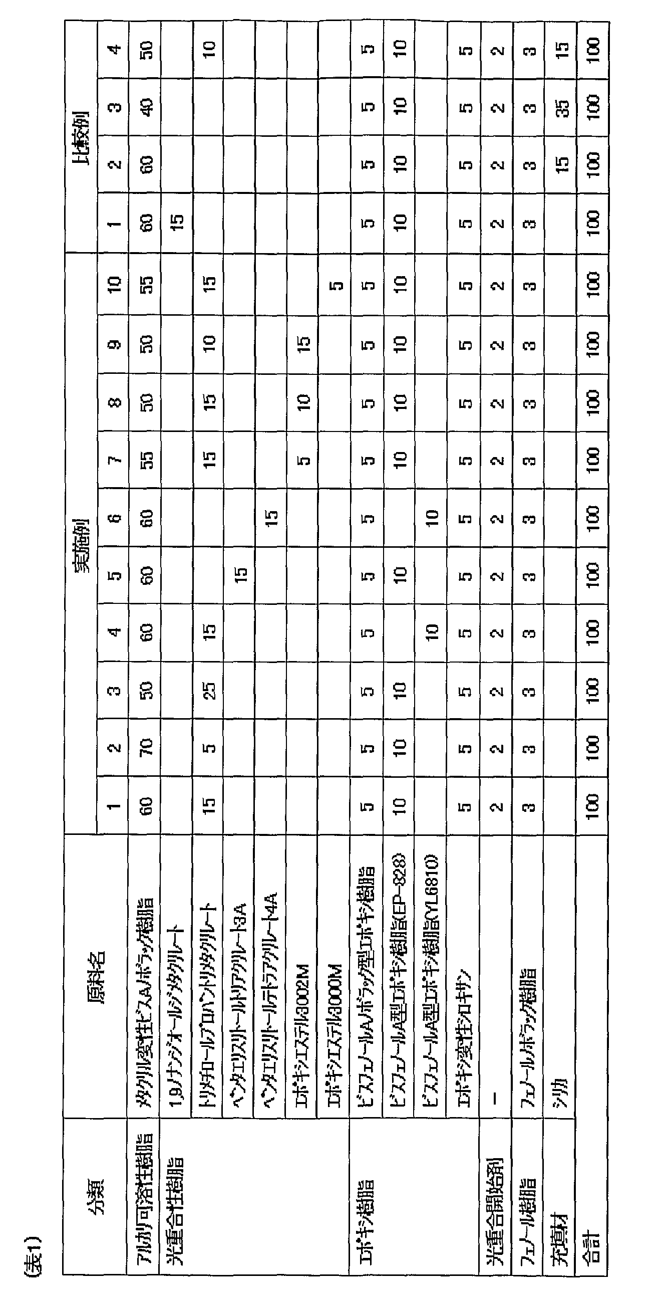

各実施例で得た接着フィルムの評価を以下のように行なった。結果を表3および表4に示した。 Evaluation of the adhesive film obtained in each example was performed as follows. The results are shown in Tables 3 and 4.
(1) 弾性率
実施例1~13、比較例1~4で得られた接着フィルムに、波長365nmの光を700mJ/cm2照射し露光を行った。次いで、接着フィルムからPETフィルムを剥がし接着層を3枚重ねて、動的粘弾性測定装置Rheo Stress RS150(HAAKE社製、測定周波数:1Hz、ギャップ間隔:100μm、測定温度範囲:25~200℃、昇温速度10℃/分)で貯蔵弾性率G´を測定し、80℃における弾性率を求めた。結果を表3および表4に示した。
(1) Elastic Modulus The adhesive films obtained in Examples 1 to 13 and Comparative Examples 1 to 4 were exposed to light having a wavelength of 365 nm by irradiation with 700 mJ / cm 2 . Next, the PET film was peeled off from the adhesive film and three adhesive layers were stacked, and a dynamic viscoelasticity measuring device Rheo Stress RS150 (manufactured by HAAKE, measurement frequency: 1 Hz, gap interval: 100 μm, measurement temperature range: 25 to 200 ° C., The storage elastic modulus G ′ was measured at a heating rate of 10 ° C./min), and the elastic modulus at 80 ° C. was determined. The results are shown in Tables 3 and 4.
(2) 透過率
厚さ25μmの接着フィルムを作製し、UV可視分光器(型番:UV-160A、(株)島津製作所製)を用い、測定波長:200~1000nmで透過率を測定し、波長365nmにおける透過率を測定値とした。結果を表3および表4に示した。
(2) Transmittance An adhesive film having a thickness of 25 μm was prepared, and the transmittance was measured at a measurement wavelength of 200 to 1000 nm using a UV-visible spectrometer (model number: UV-160A, manufactured by Shimadzu Corporation). The transmittance at 365 nm was taken as the measured value. The results are shown in Tables 3 and 4.
(3)透湿率
60℃に設定されたラミネータを用いて、接着フィルムを貼り合せ、膜厚100μmのフィルムを作製し、露光機を用いて、露光量700mJ/cm2(波長365nm)の光を照射したあとに、180℃/2時間熱硬化した。得られた硬化後のフィルムを透湿カップ法(JIS Z0208)に準じて、40℃/90%の環境下で評価し、透湿率を求めた。結果を表3および表4に示した。
(3) Moisture permeability Using a laminator set at 60 ° C., an adhesive film is laminated to produce a film with a thickness of 100 μm, and an exposure device is used to emit light with an exposure amount of 700 mJ / cm 2 (wavelength 365 nm). After the irradiation, it was heat-cured at 180 ° C./2 hours. The obtained cured film was evaluated in an environment of 40 ° C./90% in accordance with a moisture permeable cup method (JIS Z0208) to obtain a moisture permeability. The results are shown in Tables 3 and 4.
[規則26に基づく補充 17.06.2009]

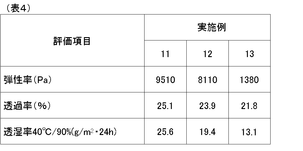
表3および表4から明らかなように、実施例1~13は硬化後の接着フィルムの弾性率、透過率および透湿率のいずれの点においても優れていた。 As is apparent from Tables 3 and 4, Examples 1 to 13 were excellent in all of the elastic modulus, transmittance and moisture permeability of the cured adhesive film.
次に、上述の接着フィルムを用いてベース基板と透明基板とを接合して得られた接着体の実施例について説明する。 Next, an example of an adhesive body obtained by joining a base substrate and a transparent substrate using the above-described adhesive film will be described.
8インチ半導体ウエハ(ベース基板)(厚み:300μm)に、実施例1~13、または、比較例1~4で得られた接着フィルムを、それぞれ、ロールラミネーター(ロール温度:60℃、速度:0.3m/分、シリンジ圧:2.0kgf/cm2)の条件でラミネートし、接着フィルム付き半導体ウエハを得た。次に、露光装置のマスクと接着フィルム付き8インチ半導体ウエハの位置合わせを波長600nmの光で行った。次に、波長365nmの光を700mJ/cm2照射し、PETフィルムを引き剥がした。さらに、2.38重量%TMAH(テトラメチルアンモニウムハイドロオキサイド)を用いて、現像液圧:0.3MPa、時間:90秒現像を行い、5mm角、幅0.6mmの形状の接着フィルムからなる枠部材を形成した。
次に、サブストレート・ボンダ(ズース・マイクロテック(株)製、SB8e)に上記枠部材を有する半導体ウエハおよび8インチ透明基板をセットし、8インチ半導体ウエハと8インチ透明基板の圧着を行い、さらに、150℃、90分の条件でポストキュアを行った。得られた8インチ半導体ウエハと8インチ透明基板の接着物を、ダイシングソーを用い、所定の大きさにダイシングし、受光装置を得た。
The adhesive films obtained in Examples 1 to 13 or Comparative Examples 1 to 4 were each applied to an 8-inch semiconductor wafer (base substrate) (thickness: 300 μm) using a roll laminator (roll temperature: 60 ° C., speed: 0). 3 m / min, syringe pressure: 2.0 kgf / cm 2 ) to obtain a semiconductor wafer with an adhesive film. Next, alignment of the mask of the exposure apparatus and the 8-inch semiconductor wafer with an adhesive film was performed with light having a wavelength of 600 nm. Next, 700 mJ / cm 2 of 365 nm wavelength light was applied to peel off the PET film. Further, using 2.38 wt% TMAH (tetramethylammonium hydroxide), a developing solution pressure: 0.3 MPa, time: development for 90 seconds, and a frame made of an adhesive film having a shape of 5 mm square and 0.6 mm width. A member was formed.
Next, a semiconductor wafer having the above frame member and an 8-inch transparent substrate are set on a substrate bonder (SB8e, manufactured by SUSS Microtech Co., Ltd.), and the 8-inch semiconductor wafer and the 8-inch transparent substrate are pressure-bonded. Further, post-cure was performed at 150 ° C. for 90 minutes. The obtained adhesive material of the 8-inch semiconductor wafer and the 8-inch transparent substrate was diced into a predetermined size using a dicing saw to obtain a light receiving device.
評価用サンプルで、以下のように評価した。結果はそれぞれ表5および表6に示した。
(4)形状保持性
上記評価用サンプルの枠部材のフロー性(つぶれ具合い)を目視により評価した。各符号は、以下の通りである。
○:熱圧着前後の枠部材の寸法に変化が無かった。
×:熱圧着後の樹脂スペーサが非常に大きくフローし、寸法、形状とも大きく変化していた。
Evaluation samples were evaluated as follows. The results are shown in Table 5 and Table 6, respectively.
(4) Shape retention The flowability (crushing condition) of the frame member of the evaluation sample was visually evaluated. Each code is as follows.
○: There was no change in the dimensions of the frame member before and after thermocompression bonding.
X: The resin spacer after thermocompression flowed very large, and the dimensions and shape were greatly changed.
(5)アンダーカット
露光および現像後の枠部材の断面を走査顕微鏡で観察した結果を図6に示す。比較例2の接着フィルムには、17μmのアンダーカットが観察された(図6(c))。また、比較例3の接着フィルムには、11μmのアンダーカットが観察された(図6(b))。一方、実施例1の接着フィルムには、5μmのアンダーカットが観察された(図6(a))。表5および表6では、アンダーカットが5μm以下のものを○、5μmより大きいものを×と示した。
(5) Undercut FIG. 6 shows the result of observing the cross section of the frame member after exposure and development with a scanning microscope. An undercut of 17 μm was observed in the adhesive film of Comparative Example 2 (FIG. 6C). Further, an undercut of 11 μm was observed in the adhesive film of Comparative Example 3 (FIG. 6B). On the other hand, an undercut of 5 μm was observed in the adhesive film of Example 1 (FIG. 6A). In Tables 5 and 6, those having an undercut of 5 μm or less are indicated by ◯, and those having an undercut of more than 5 μm are indicated by ×.
なお、図6(d)は、従来の接着フィルムを用いて同様な評価用サンプル(以下、従来品という)を作製し、枠部材のアンダーカットを観察したものである。このサンプルでは、27μmのアンダーカットが観察された。図7は、実施例1、比較例2,3および従来品の接着フィルムについて、アンダーカット量と光透過率との関係をグラフにしたものである。光透過率が向上すると、アンダーカット量が低減されることが示された。 Note that FIG. 6D shows a similar evaluation sample (hereinafter referred to as a conventional product) produced using a conventional adhesive film, and the undercut of the frame member observed. In this sample, an undercut of 27 μm was observed. FIG. 7 is a graph showing the relationship between the undercut amount and the light transmittance of Example 1, Comparative Examples 2 and 3, and conventional adhesive films. It was shown that the amount of undercut is reduced when the light transmittance is improved.
(6)残渣
露光および現像後、受光部を走査顕微鏡で観察したところ、比較例2の接着フィルムでは、図8(a)に示す異物(タイプA)、図9(a)に示す異物(タイプB)がウェハ上に観察された。図8(a)で示されるタイプAの異物を拡大すると、樹脂組成物由来の成分が認められた(図8(b))。図8(b)において点線で囲む部分を拡大して観察すると、シリカフィラーが観察された(図8(c))。図9(a)で示されるタイプBは液体の異物であった(図9(a))。図9(a)で示されるタイプBの異物を拡大すると、シリカフィラーが観察されたが、樹脂組成物由来の成分は認められなかった(図9(b))。比較例1の接着フィルムでは、図8で示すようなタイプAの異物は観察されなかったが、タイプBの異物は観察された。実施例1~13の接着フィルムでは、タイプA、Bいずれの異物も観察されなかった。なお、表5および表6では、ベース基板または透明基板上に異物が観察されなかったものを○、異物が観察されたものを×と示した。
(6) Residue After exposure and development, the light receiving part was observed with a scanning microscope. As a result, in the adhesive film of Comparative Example 2, the foreign matter (type A) shown in FIG. 8 (a) and the foreign matter (type) shown in FIG. B) was observed on the wafer. When the type A foreign material shown in FIG. 8A was enlarged, components derived from the resin composition were observed (FIG. 8B). When the portion surrounded by the dotted line in FIG. 8B was enlarged and observed, silica filler was observed (FIG. 8C). Type B shown in FIG. 9A was a liquid foreign substance (FIG. 9A). When the type B foreign matter shown in FIG. 9A was enlarged, silica filler was observed, but no component derived from the resin composition was observed (FIG. 9B). In the adhesive film of Comparative Example 1, no type A foreign matter as shown in FIG. 8 was observed, but type B foreign matter was observed. In the adhesive films of Examples 1 to 13, no foreign matter of type A or B was observed. In Tables 5 and 6, the case where no foreign matter was observed on the base substrate or the transparent substrate was indicated as ◯, and the case where foreign matter was observed was indicated as ×.
(7)結露
温度60℃、湿度90%の条件下で、500時間処理したあと、温度25℃、湿度50%の環境に出し、評価用サンプルのガラス基板の内側が結露するか顕微鏡で観察した。結果は表5および表6に示した。表5および表6では、結露がないものを○、結露が発生したものを×と示した。
(7) Condensation After processing for 500 hours under conditions of a temperature of 60 ° C. and a humidity of 90%, the sample was put out in an environment of a temperature of 25 ° C. and a humidity of 50%, and the inside of the glass substrate of the sample for evaluation was observed with a microscope. . The results are shown in Tables 5 and 6. In Tables 5 and 6, those having no condensation were indicated as ◯, and those having condensation were indicated as ×.

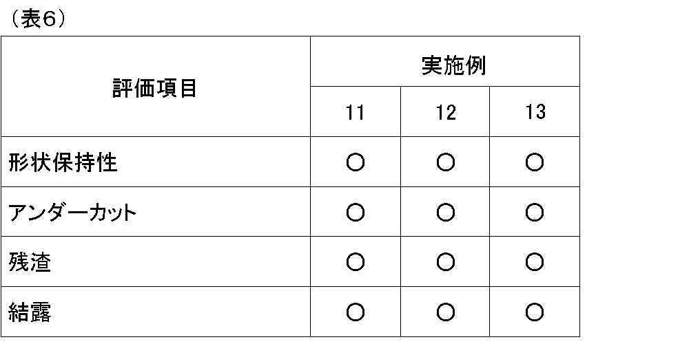
表5および表6から明らかなように、実施例1~13は受光装置の形状保持性に優れていた。また、枠部材のアンダーカットも少なかった。さらに、ウェハ上に残渣および結露が観察されず良好な信頼性を示した。 As is clear from Tables 5 and 6, Examples 1 to 13 were excellent in the shape retention of the light receiving device. Moreover, there was little undercut of the frame member. Furthermore, no residue or condensation was observed on the wafer, indicating good reliability.
Claims (11)
前記受光部が設けられたベース基板と、
前記ベース基板及び前記受光部に対向配置された透明基板と、
前記ベース基板と前記透明基板との間に前記受光部を囲むように配置された枠部材と、
を備え、
前記枠部材は、樹脂組成物が硬化されてなるものであり、
前記樹脂組成物は、
アルカリ可溶性樹脂と、
光重合性樹脂と、
9重量%以下の無機充填材と、
を含み、
前記光重合性樹脂は、アクリル系多官能モノマーを含み、
前記枠部材は、以下の(a)及び(b)の条件を満たす受光装置。
(a)JIS Z0208 B法により測定された前記枠部材の透湿率が12[g/m2・24h]以上
(b)水銀ランプで全波長の光を露光し、その積算露光量が、i線(365nm)の光で700mJ/cm2になるように露光した後の、前記枠部材の80℃における弾性率が100Pa以上。 At least one light receiving unit;
A base substrate provided with the light receiving portion;
A transparent substrate disposed opposite to the base substrate and the light receiving unit;
A frame member disposed so as to surround the light receiving portion between the base substrate and the transparent substrate;
With
The frame member is formed by curing a resin composition,
The resin composition is
An alkali-soluble resin;
A photopolymerizable resin;
9% by weight or less of inorganic filler,
Including
The photopolymerizable resin includes an acrylic polyfunctional monomer,
The frame member is a light receiving device that satisfies the following conditions (a) and (b).
(A) Moisture permeability of the frame member measured by JIS Z0208 B method is 12 [g / m 2 · 24 h] or more (b) Light of all wavelengths is exposed with a mercury lamp, and the integrated exposure amount is i The elastic modulus at 80 ° C. of the frame member after exposure to 700 mJ / cm 2 with light of a line (365 nm) is 100 Pa or more.
前記接着フィルムに対し、電子線を選択的に照射し、少なくとも前記ベース基板上の前記受光部を囲む領域、又は、前記透明基板を前記ベース基板と対向配置させた際に、前記透明基板の前記受光部を覆う各領域を囲む領域に前記接着フィルムを残す工程と、
前記ベース基板および前記透明基板を対向配置させて、前記接着フィルムにより接着する工程と、
前記ベース基板と、前記透明基板と、前記ベース基板および前記透明基板との間に設けられるとともに、前記接着フィルムにより構成され、前記受光部を囲むように配置された枠部材と、を有する受光装置を得る工程と、
を含み、
前記樹脂組成物は、
アルカリ可溶性樹脂と、
光重合性樹脂と、
9重量%以下の無機充填材と、
を含み、
前記光重合性樹脂は、アクリル系多官能モノマーを含み、
前記枠部材は、以下の(a)及び(b)の条件を満たす受光装置の製造方法。
(a)JIS Z0208 B法により測定された前記枠部材の透湿率が12[g/m2・24h]以上
(b)水銀ランプで全波長の光を露光し、その積算露光量が、i線(365nm)の光で700mJ/cm2になるように露光した後の、前記枠部材の80℃における弾性率が100Pa以上。 A step of attaching an adhesive film made of an electron beam curable resin composition to cover the base substrate or the transparent substrate on a base substrate provided with at least one or more light receiving units, or a transparent substrate;
The adhesive film is selectively irradiated with an electron beam, and at least the region surrounding the light receiving portion on the base substrate, or the transparent substrate when the transparent substrate is disposed opposite to the base substrate, the transparent substrate. Leaving the adhesive film in a region surrounding each region covering the light receiving unit;
A step of arranging the base substrate and the transparent substrate to face each other and bonding them with the adhesive film;
A light receiving device having the base substrate, the transparent substrate, and a frame member that is provided between the base substrate and the transparent substrate and is configured by the adhesive film so as to surround the light receiving unit. And obtaining
Including
The resin composition is
An alkali-soluble resin;
A photopolymerizable resin;
9% by weight or less of inorganic filler,
Including
The photopolymerizable resin includes an acrylic polyfunctional monomer,
The frame member is a method for manufacturing a light receiving device that satisfies the following conditions (a) and (b).
(A) Moisture permeability of the frame member measured by JIS Z0208 B method is 12 [g / m 2 · 24 h] or more (b) Light of all wavelengths is exposed with a mercury lamp, and the integrated exposure amount is i The elastic modulus at 80 ° C. of the frame member after exposure to 700 mJ / cm 2 with light of a line (365 nm) is 100 Pa or more.
Priority Applications (5)
| Application Number | Priority Date | Filing Date | Title |
|---|---|---|---|
| JP2010514381A JPWO2009144951A1 (en) | 2008-05-30 | 2009-05-29 | Light receiving device and method for manufacturing light receiving device |
| KR1020107029055A KR20110015444A (en) | 2008-05-30 | 2009-05-29 | Light receiving device, manufacturing method of light receiving device |
| US12/993,368 US20110101484A1 (en) | 2008-05-30 | 2009-05-29 | Light-receiving device and method of manufacturing the same |
| EP09754459A EP2282342A1 (en) | 2008-05-30 | 2009-05-29 | Light-receiving device and production therof |
| CN2009801203316A CN102047425A (en) | 2008-05-30 | 2009-05-29 | Light receiving device and manufacturing method thereof |
Applications Claiming Priority (4)
| Application Number | Priority Date | Filing Date | Title |
|---|---|---|---|
| JP2008-143199 | 2008-05-30 | ||
| JP2008143199 | 2008-05-30 | ||
| JP2008307046 | 2008-12-02 | ||
| JP2008-307046 | 2008-12-02 |
Publications (1)
| Publication Number | Publication Date |
|---|---|
| WO2009144951A1 true WO2009144951A1 (en) | 2009-12-03 |
Family
ID=41376840
Family Applications (1)
| Application Number | Title | Priority Date | Filing Date |
|---|---|---|---|
| PCT/JP2009/002382 Ceased WO2009144951A1 (en) | 2008-05-30 | 2009-05-29 | Light-receiving device and production therof |
Country Status (7)
| Country | Link |
|---|---|
| US (1) | US20110101484A1 (en) |
| EP (1) | EP2282342A1 (en) |
| JP (1) | JPWO2009144951A1 (en) |
| KR (1) | KR20110015444A (en) |
| CN (1) | CN102047425A (en) |
| TW (1) | TW201007933A (en) |
| WO (1) | WO2009144951A1 (en) |
Cited By (1)
| Publication number | Priority date | Publication date | Assignee | Title |
|---|---|---|---|---|
| WO2010113759A1 (en) * | 2009-03-31 | 2010-10-07 | 住友ベークライト株式会社 | Film for resin spacer, light-receiving device and method for manufacturing same, and mems device and method for manufacturing same |
Families Citing this family (3)
| Publication number | Priority date | Publication date | Assignee | Title |
|---|---|---|---|---|
| JP5634380B2 (en) | 2011-10-31 | 2014-12-03 | アオイ電子株式会社 | Light receiving device and manufacturing method thereof |
| CN104126331B (en) * | 2012-02-24 | 2016-09-14 | 三井化学株式会社 | Optics face encapsulation compositions, the encapsulation of optics face sheet, display and the manufacture method of display |
| US9481572B2 (en) * | 2014-07-17 | 2016-11-01 | Texas Instruments Incorporated | Optical electronic device and method of fabrication |
Citations (4)
| Publication number | Priority date | Publication date | Assignee | Title |
|---|---|---|---|---|
| JPS6191212A (en) * | 1984-10-12 | 1986-05-09 | Dainippon Ink & Chem Inc | Resin composition for electrical laminated sheet |
| JP2004296453A (en) | 2003-02-06 | 2004-10-21 | Sharp Corp | Solid-state imaging device, semiconductor wafer, module for optical device, method for manufacturing solid-state imaging device, and method for manufacturing module for optical device |
| JP2008022001A (en) * | 2007-07-09 | 2008-01-31 | Sumitomo Bakelite Co Ltd | Light receiving device and method for manufacturing light receiving device |
| JP2008042186A (en) * | 2006-07-11 | 2008-02-21 | Sumitomo Bakelite Co Ltd | Light receiving device and method for manufacturing light receiving device |
-
2009
- 2009-05-29 KR KR1020107029055A patent/KR20110015444A/en not_active Withdrawn
- 2009-05-29 WO PCT/JP2009/002382 patent/WO2009144951A1/en not_active Ceased
- 2009-05-29 CN CN2009801203316A patent/CN102047425A/en active Pending
- 2009-05-29 JP JP2010514381A patent/JPWO2009144951A1/en not_active Withdrawn
- 2009-05-29 EP EP09754459A patent/EP2282342A1/en not_active Withdrawn
- 2009-05-29 US US12/993,368 patent/US20110101484A1/en not_active Abandoned
- 2009-06-01 TW TW098117957A patent/TW201007933A/en unknown
Patent Citations (4)
| Publication number | Priority date | Publication date | Assignee | Title |
|---|---|---|---|---|
| JPS6191212A (en) * | 1984-10-12 | 1986-05-09 | Dainippon Ink & Chem Inc | Resin composition for electrical laminated sheet |
| JP2004296453A (en) | 2003-02-06 | 2004-10-21 | Sharp Corp | Solid-state imaging device, semiconductor wafer, module for optical device, method for manufacturing solid-state imaging device, and method for manufacturing module for optical device |
| JP2008042186A (en) * | 2006-07-11 | 2008-02-21 | Sumitomo Bakelite Co Ltd | Light receiving device and method for manufacturing light receiving device |
| JP2008022001A (en) * | 2007-07-09 | 2008-01-31 | Sumitomo Bakelite Co Ltd | Light receiving device and method for manufacturing light receiving device |
Cited By (1)
| Publication number | Priority date | Publication date | Assignee | Title |
|---|---|---|---|---|
| WO2010113759A1 (en) * | 2009-03-31 | 2010-10-07 | 住友ベークライト株式会社 | Film for resin spacer, light-receiving device and method for manufacturing same, and mems device and method for manufacturing same |
Also Published As
| Publication number | Publication date |
|---|---|
| KR20110015444A (en) | 2011-02-15 |
| TW201007933A (en) | 2010-02-16 |
| EP2282342A1 (en) | 2011-02-09 |
| CN102047425A (en) | 2011-05-04 |
| JPWO2009144951A1 (en) | 2011-10-06 |
| US20110101484A1 (en) | 2011-05-05 |
Similar Documents
| Publication | Publication Date | Title |
|---|---|---|
| JP4091969B1 (en) | Light receiving device and method for manufacturing light receiving device | |
| KR20100022019A (en) | Resin composition, resin spacer film, and semiconductor device | |
| JPWO2010119647A1 (en) | Photosensitive resin composition, adhesive film, and light receiving device | |
| WO2010113759A1 (en) | Film for resin spacer, light-receiving device and method for manufacturing same, and mems device and method for manufacturing same | |
| JP5338663B2 (en) | Manufacturing method of electronic device | |
| WO2011046181A1 (en) | Resin composition, semiconductor wafer-bonded body, and semiconductor device | |
| TWI459135B (en) | Photosensitive resin composition, photosensitive adhesive film and light receiving device | |
| WO2009144951A1 (en) | Light-receiving device and production therof | |
| WO2010095593A1 (en) | Semiconductor wafer assembly, method for producing semiconductor wafer assembly, and semiconductor device | |
| WO2011034025A1 (en) | Film for forming spacer, method for manufacturing semiconductor wafer bonded body, semiconductor wafer bonded body, and semiconductor device | |
| WO2010095592A1 (en) | Method for producing semiconductor wafer assembly, semiconductor wafer assembly, and semiconductor device | |
| JP2008042186A (en) | Light receiving device and method for manufacturing light receiving device | |
| JP4694804B2 (en) | Adhesive film and hollow package | |
| JP3958310B2 (en) | Resin composition and adhesive film | |
| JP2010008639A (en) | Photosensitive resin composition, adhesive film and light receiving device | |
| JP2008022001A (en) | Light receiving device and method for manufacturing light receiving device | |
| JP2009021542A (en) | Light receiving device and method for manufacturing light receiving device | |
| JP2011066167A (en) | Film for forming spacer, method for manufacturing semiconductor wafer bonded body, semiconductor wafer bonded body, and semiconductor device | |
| WO2011118600A1 (en) | Method for manufacturing a semiconductor wafer assembly, semiconductor wafer assembly, and semiconductor device | |
| JP2008091399A (en) | Manufacturing method of light receiving device | |
| JP4811320B2 (en) | Resin composition and adhesive film | |
| JPWO2010103903A1 (en) | Spacer forming film, semiconductor wafer, and semiconductor device | |
| WO2011030797A1 (en) | Method for producing semiconductor wafer assembly, semiconductor wafer assembly, and semiconductor device | |
| JP2013105941A (en) | Resin composition, semiconductor device, and method for manufacturing semiconductor device |
Legal Events
| Date | Code | Title | Description |
|---|---|---|---|
| WWE | Wipo information: entry into national phase |
Ref document number: 200980120331.6 Country of ref document: CN |
|
| 121 | Ep: the epo has been informed by wipo that ep was designated in this application |
Ref document number: 09754459 Country of ref document: EP Kind code of ref document: A1 |
|
| WWE | Wipo information: entry into national phase |
Ref document number: 2010514381 Country of ref document: JP |
|
| WWE | Wipo information: entry into national phase |
Ref document number: 2009754459 Country of ref document: EP |
|
| WWE | Wipo information: entry into national phase |
Ref document number: 12993368 Country of ref document: US |
|
| NENP | Non-entry into the national phase |
Ref country code: DE |
|
| ENP | Entry into the national phase |
Ref document number: 20107029055 Country of ref document: KR Kind code of ref document: A |