WO1997036210A1 - Perfluoroether release coatings for organic photoreceptors - Google Patents
Perfluoroether release coatings for organic photoreceptors Download PDFInfo
- Publication number
- WO1997036210A1 WO1997036210A1 PCT/US1997/002524 US9702524W WO9736210A1 WO 1997036210 A1 WO1997036210 A1 WO 1997036210A1 US 9702524 W US9702524 W US 9702524W WO 9736210 A1 WO9736210 A1 WO 9736210A1
- Authority
- WO
- WIPO (PCT)
- Prior art keywords
- group
- carbon atoms
- perfluoroether
- integer
- formula
- Prior art date
- Legal status (The legal status is an assumption and is not a legal conclusion. Google has not performed a legal analysis and makes no representation as to the accuracy of the status listed.)
- Ceased
Links
Classifications
-
- G—PHYSICS
- G03—PHOTOGRAPHY; CINEMATOGRAPHY; ANALOGOUS TECHNIQUES USING WAVES OTHER THAN OPTICAL WAVES; ELECTROGRAPHY; HOLOGRAPHY
- G03G—ELECTROGRAPHY; ELECTROPHOTOGRAPHY; MAGNETOGRAPHY
- G03G5/00—Recording members for original recording by exposure, e.g. to light, to heat, to electrons; Manufacture thereof; Selection of materials therefor
- G03G5/14—Inert intermediate or cover layers for charge-receiving layers
- G03G5/147—Cover layers
- G03G5/14708—Cover layers comprising organic material
- G03G5/14713—Macromolecular material
- G03G5/14786—Macromolecular compounds characterised by specific side-chain substituents or end groups
-
- G—PHYSICS
- G03—PHOTOGRAPHY; CINEMATOGRAPHY; ANALOGOUS TECHNIQUES USING WAVES OTHER THAN OPTICAL WAVES; ELECTROGRAPHY; HOLOGRAPHY
- G03G—ELECTROGRAPHY; ELECTROPHOTOGRAPHY; MAGNETOGRAPHY
- G03G5/00—Recording members for original recording by exposure, e.g. to light, to heat, to electrons; Manufacture thereof; Selection of materials therefor
- G03G5/14—Inert intermediate or cover layers for charge-receiving layers
- G03G5/147—Cover layers
- G03G5/14708—Cover layers comprising organic material
- G03G5/14713—Macromolecular material
- G03G5/14747—Macromolecular material obtained otherwise than by reactions only involving carbon-to-carbon unsaturated bonds
- G03G5/14769—Other polycondensates comprising nitrogen atoms with or without oxygen atoms in the main chain
-
- G—PHYSICS
- G03—PHOTOGRAPHY; CINEMATOGRAPHY; ANALOGOUS TECHNIQUES USING WAVES OTHER THAN OPTICAL WAVES; ELECTROGRAPHY; HOLOGRAPHY
- G03G—ELECTROGRAPHY; ELECTROPHOTOGRAPHY; MAGNETOGRAPHY
- G03G5/00—Recording members for original recording by exposure, e.g. to light, to heat, to electrons; Manufacture thereof; Selection of materials therefor
- G03G5/14—Inert intermediate or cover layers for charge-receiving layers
- G03G5/147—Cover layers
- G03G5/14708—Cover layers comprising organic material
- G03G5/14713—Macromolecular material
- G03G5/14747—Macromolecular material obtained otherwise than by reactions only involving carbon-to-carbon unsaturated bonds
- G03G5/14773—Polycondensates comprising silicon atoms in the main chain
Definitions
- the present invention relates to a photoreceptor element which is capable of transferring toner images to a receptor. More specifically, this invention relates to a release coating for the photoreceptor element.
- Electrophotography forms the technical basis for various well known imaging processes, including photocopying and laser printing.
- the basic electrophotographic process involves placing a uniform electrostatic charge on a photoreceptor element; imagewise exposing the photoreceptor element to light, thereby dissipating the charge in the exposed areas; developing the resulting electrostatic latent image with a toner; and transferring the toner image from the photoreceptor element to a final substrate, such as paper or film, either by direct transfer or via an intermediate transfer material.
- photoreceptor element may be a flat plate, a rotatable drum, or a continuous belt which is supported and circulated by rollers. All photoreceptor elements have a photoconductive layer which conducts electric current only when it is being exposed to light.
- the photoconductive layer is generally affixed to an electroconductive support.
- the surface of the photoconductor is either negatively or positively charged such that when light strikes the photoconductive layer, charge is conducted through the photoconductor in that region to neutralize the surface potential in the illuminated region.
- An optional barrier layer may be used over the photoconductive layer to protect the photoconductive layer and extend the service life of the photoconductive layer.
- a positively charged toner is attracted to those areas of the photoreceptor element which retain a charge after the imagewise exposure, thereby forming a toner image which corresponds to the electrostatic latent image.
- the toner need not be positively charged. Some toners are attracted to the areas of the photoconductor element where the charge has been dissipated.
- the toner may be either a powdered material comprising a blend of polymer and colored particulates, typically carbon, or a liquid material of finely divided solids dispersed in an insulating liquid. Liquid toners are often preferable because they are capable of giving higher resolution images.
- the toner image may be transferred to the substrate or an intermediate carrier by means of heat, pressure, a combination of heat and pressure, or electrostatic assist.
- a common problem that arises at this stage of electrophotographic imaging is poor transfer from the photoconductor to the receptor or intermediate carrier. Poor transfer may be manifested by low transfer efficiency and low image resolution. Low transfer efficiency results in images that are light and/or speckled. Low image resolution results in images that are fuzzy.
- the release layer is applied over the photoconductive layer or over the barrier layer if a barrier layer is being used.
- the release layer must adhere well to the photoconductive or barrier layer without the need for adhesives. Moreover, the release layer must not significantly interfere with the charge transport characteristics of the photoconductor construction.
- Typical release coatings known in the electrophotographic arts include silicone polymers such as those disclosed in U.S. Pat. No. 4,600,673.
- Conventional silicone polymer release materials tend to swell significantly in the hydrocarbon solvents which are used as carrier liquids in electrophotography. Swollen polymers generally have reduced toughness, and siloxanes, which typically do not have good tensile properties, are very easily scratched when swollen. Solvent resistance may be improved by adding fillers to or by cross-linking the polymer. However, cross-linked or filled systems tend to have increased the surface energy causing a decreased release performance.
- U.S. Pat. No. 4,996,125 discloses the use of a perfluoroalkyl polyether and its derivatives as a lubricating layer.
- This patent includes an Example having a perfluoroether-urethane polymer lubricating layer on a electrophotographic photoreceptor. Images were made using a FX 4300 copier (Fuji Xerox Co., Ltd.), which is a copier that uses dry toner.
- FX 4300 copier Fluji Xerox Co., Ltd.
- the present inventors tested similar release coatings with a liquid toner system they found that such perfluoroether-urethane polymer release coats had poor resistance to liquid toner and a relatively high peel force.
- the release layer should be mechanically durable as to withstand abrasion of the various rollers and scrapers which contact the photoreceptor element.
- the release layer must also be resistant to the toner carrier liquids.
- the present invention provides a photoreceptor element comprising an electroconductive substrate, a photoconductor layer, and a release layer which displays good release properties, as well as good durability and resistance to toner carrier liquids.
- the release layer comprises a perfluoroether urethane which includes silicon atoms (Si), via a silane group.
- the release layer comprises a perfluoroether urethane which is the reaction product of a di-functional perfluoroether, a diisocyanate, an amino functional silane, and, optionally, a diol chain extender.
- the perfluoroether urethane has the following structure: C-[B-A-B-D] x -[B-A] y -B-C, wherein A, B, C, and D are defined by the perfluoroether, the diisocyanate, the amino functional silane, and the diol chain extender, respectively; x is an integer from 0 to 10, and y is an integer from 1 to 10.
- Use of the diol chain extender, by having x greater than 1, is optional but preferred because it increases the resistance of the release layer to toner carrier liquids.
- This release layer on an organic photoconductor has good toner release performance and good resistance to wiping, swelling and crazing with a toner carrier liquid.
- the perfluoroether urethane release coating can be used as a durable overcoat for an organic photoconductor used with liquid toners.
- the photoreceptor element of this invention comprises an electroconductive substrate which supports at least a photoconductor layer and a release layer.
- the photoconductors of this invention may be of a drum type construction, a belt construction, a flat plate, or any other construction known in the art.
- Electroconductive substrates for photoconductive systems are well known in the art and are two general classes: (a) self-supporting layers or blocks of conducting metals, or other highly conducting materials; and (b) insulating materials such as polymer sheets, glass, or paper, to which a thin conductive coating, such as vapor coated aluminum, has been applied (e.g., aluminized polyethylene terephthalate).
- insulating materials such as polymer sheets, glass, or paper, to which a thin conductive coating, such as vapor coated aluminum, has been applied (e.g., aluminized polyethylene terephthalate).
- the photoconductive layer can be any type known in the art, including an inorganic photoconductor material in particulate form dispersed in a binder or, more preferably, an organic photoconductor material.
- the thickness of the photoconductor layer is dependent on the material used, but is typically in the range of 5 to 150 ⁇ m.
- the photoconductive layer can be a bilayer construction consisting of a charge generating layer and a charge transport layer.
- the charge generating layer is typically about 0.01 to 20 ⁇ m thick and includes a material which is capable of absorbing light to generate charge carriers, such as a dyestuff or pigment.
- the charge transport layer is typically 10-20 ⁇ m thick and includes a material capable of transporting the generated charge carriers, such as poly-N-vinylcarbazoles or derivatives of bis-(benzocarbazole)- phenylmethane in a suitable binder.
- the charge generation layer is typically located between the conductive substrate and the charge transport layer.
- a photoreceptor element is usually formed by coating the conductive substrate with a thin coating of a charge generation layer, overcoated by a relatively thick coating of a charge transport layer.
- the surface of the photoreceptor element is negatively charged.
- hole/electron pairs are formed at or near the charge generation layer/charge transport layer interface. Electrons migrate through the charge generation layer to the conductive substrate while holes migrate through the charge transport layer to neutralize the negative charge on the surface. In this way, charge is neutralized in the light-struck areas.
- an inverted bilayer system may be used. Photoconductor elements having an inverted bilayer organic photoconductor material require positive charging which results in less deterioration of the photoreceptor surface.
- the conductive substrate is coated with a relatively thick coating (preferably, 5-20 ⁇ m) of a charge transport layer, overcoated with a relatively thin (preferably, 0.01 to 5 ⁇ m) coating of a charge generation layer.
- the surface of the photo-receptor is positively charged.
- hole/electron pairs are formed at or near the charge generation layer/charge transport layer interface. Electrons migrate through the charge generation layer to neutralize the positive charge on the surface while holes migrate through the charge transport layer to the conductive substrate. In this way, charge is again neutralized in the light-struck areas.
- Single layer photoconductive layers are also common.
- a single-layer construction a mixture of charge generation and charge transport materials are incorporated into one layer. This layer has both charge generating and charge transport capabilities. Examples of single-layer organic photoconductive layers are described in U.S. Pat. Nos. 4,853,310; 5,087,540; and 3,816,118.
- a disadvantage of single layer constructions is that they tend suffer fatigue on repeated cycling and cannot be used in high speed systems.
- Suitable charge generating materials for use in a single layer photoconductor and/or the charge generating layer of a bilayer photoconductor include azo pigments, perylene pigments, phthalocyanine pigments, squaraine pigments, and two phase aggregate materials.
- the two phase aggregate materials contain a light sensitive filamentary crystalline phase dispersed in an amorphous matrix.
- the charge transport material transports the charge (holes or electrons) from the site of generation through the bulk of the film.
- Charge transport materials are typically either molecularly doped polymers or active transport polymers. Suitable charge transport materials include enamines, hydrazones, oxadiazoles, oxazoles, pyrazolines, triarylamines, and triarylmethanes.
- a suitable active transport polymer is polyvinyl carbazole. Especially preferred transport materials are polymers such as poly(N-vinyl carbazole) and acceptor doped poly(N- vinylcarbazole). Additional materials are disclosed in Borsenberger and Weiss, Photoreceptors: Organic Photoconductors, Ch. 9 Handbook of Imaging Materials, ed. Arthur S. Diamond, Marcel Dekker, Inc. 1991.
- Suitable binder resins for the organic photoconductor materials include polyesters, polyvinyl acetate, polyvinyl chloride, polyvinylidene chloride, polycarbonates, polyvinyl butyral, polyvinyl acetoacetal, polyvinyl formal, polyacrylonitrile, polymethyl methacrylate, polyacrylates, polyvinyl carbazoles, copolymers of monomers used in the above-mentioned polymers, vinyl chloride/vinyl acetate/vinyl alcohol terpolymers, vinyl chloride/vinyl acetate/maleic acid terpolymers, ethylene/vinyl acetate copolymers, vinyl chloride/vinylidene chloride copolymers, cellulose polymers and mixtures thereof.
- Suitable solvents used in coating the organic photoconductor materials include nitrobenzene, chlorobenzene, dichlorobenzene, trichloroethylene, tetrahydrofuran, and the like.
- Inorganic photoconductors such as, for example, zinc oxide, titanium dioxide, cadmium sulfide, and antimony sulfide, dispersed in an insulating binder are well known in the art and may be used in any of their conventional versions with the addition of sensitizing dyes where required.
- the preferred binders are resinous materials, including, but not limited to, styrenebutadiene copolymers, modified acrylic polymers, vinyl acetate polymers, styrene-alkyd resins, soya-alkyl resins, polyvinylchloride, polyvinylidene chloride, acrylonitrile, polycarbonate, polyacrylic and methacrylic esters, polystyrene, polyesters, and combinations thereof.
- resinous materials including, but not limited to, styrenebutadiene copolymers, modified acrylic polymers, vinyl acetate polymers, styrene-alkyd resins, soya-alkyl resins, polyvinylchloride, polyvinylidene chloride, acrylonitrile, polycarbonate, polyacrylic and methacrylic esters, polystyrene, polyesters, and combinations thereof.
- the release layer of this invention comprises a perfluorourethane preferably having the following structure:
- A is derived from a di-functional perfluoroether
- B is derived from a diisocyanate
- C is derived from an amino functional silane
- D is derived from a diol chain extender
- x is an integer from 0 to 10
- y is an integer from 1 to 10.
- x is 1 to 5 and y is 1 to 3.
- A has the formula
- each R is a divalent linking group
- each RF independently is perfluorinated oxyalkylene group from 1 to 5, more preferably 1 to 2 carbon atoms
- m is an integer of from 5 to 50. More preferably A has the formula
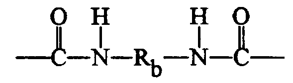
- B has the formula
- Rb is a divalent organic linking group.
- C has the formula
- Ri, R 2 , and R 3 are independently hydrogen, alkyl groups, preferably of 1 to 5 carbon atoms, aryl groups, and alkoxy groups, preferably of 1 to 5 carbon atoms, provided that at least one of Ri, R 2 , and R 3 , is a hydrogen or, more preferably an alkoxy group;
- R is an alkylene group, alkenylene group, or arylene group
- R A is a hydrogen, alkyl groups of 1 to 5 carbon atoms, or an aryl group, and d is an integer up to 10, preferably 1 to 5.
- D has the formula wherein Rd is a divalent organic linking group.
- the inventive release layer may be formed by initially reacting a di- functional perfluoroether, such as a perfluoroether diol with a diisocyanate. An amino silane is then added to the mixture and the reaction is completed.
- a di- functional perfluoroether such as a perfluoroether diol
- an amino silane is then added to the mixture and the reaction is completed.
- the perfluoroether diol and diisocyanate are further reacted with a diol chain extender before the addition of the silane.
- the equivalent ratios of the reactants are 1 equivalent of di-functional perfluoroether: 2 equivalents of diisocyanate: 1.5-1.9 equivalents of aminofunctional silane:0.1-0.5 equivalents of diol chain extender.
- Suitable perfluoroether diols include, but are not limited to, those having the formula:
- R is a divalent linking group, preferably a substituted or unsubstituted alkylene group of 1 to 5 carbon atoms or a carbon to oxygen bond, each R F independently is perfluonnated oxyalkylene group from 1 to 5, more preferably 1 to 2, carbon atoms, m is an integer of from 5 to 50.
- R is a divalent linking group, preferably a substituted or unsubstituted alkylene group of 1 to 5 carbon atoms or a carbon to oxygen bond
- each R F independently is perfluonnated oxyalkylene group from 1 to 5, more preferably 1 to 2, carbon atoms
- m is an integer of from 5 to 50.
- perfluoroether diols have the formula
- diisocyanate Any known diisocyanate may be used. Suitable diisocyanates include but are not limited to l,3-bis(l-isocyanato-l-methylethyl)-benzene; 1,12-diisocyanato- dodecane; 4,4'-methylenebis(cyclohexyl isocyanate); 4,4'-methylenebis(phenyl isocyanate); 4,4'-methylenebis(2,6-diethylphenyl isocyanate); 3,3 -dimethoxy- 4,4'-biphenylenediisocyanate; 3,3'-dimethyldiphenylmethane-4,4'-diisocyanate; 1,4-phenylene diisocyanate; 1,4-diisocyanatobutane; 1,3-phenylenediisocyanate; m-xylene diisocyanate; 1,8-diisocyanatooctane; trans- 1,4-
- Suitable silanes include those having the formula.
- Ri, R 2 , and R 3 are independently hydrogen, alkyl groups, preferably of 1 to 5 carbon atoms, aryl groups, and alkoxy groups, preferably of 1 to 5 carbon atoms, provided that at least one of Ri, R 2 , and R 3 , is a hydrogen or, more preferably an alkoxy group;
- R is an alkylene group, alkenylene group or arylene group
- ⁇ is a hydrogen, an alkyl group of 1 to 5 carbon atoms, or an aryl group
- d is an integer up to 10, preferably 1 to 5.
- Trialkoxysilyl-aminoalkanes are preferred.
- An especially prefened silane is 1 -triethoxysilyl-3 -N-methylaminopropane.
- Suitable chain extending diols include alkylene diols, arylene diols, alkenylene diols. Alkylene diols of 1 to 10 carbon atoms are preferred.
- the above release layer is mechanically durable and very resistant to hydrocarbons which typically serve as toner carrier liquids.
- the thickness of the release layer is at least 0.1 ⁇ m. The maximum thickness is dependent on the photoconductor material, but preferably is 0.3 to 3 ⁇ m, more preferably 0.5 to 1.0 ⁇ m.
- the photoreceptor element of this invention may further comprise a barrier layer between the photoconductor layer and the release layer.
- the barrier layer protects the photoconductor layer from the toner carrier liquid and other compounds which might damage the photoconductor.
- the barrier layer also protects the photoconductive layer from damage that could occur from charging the photoreceptor element with a high voltage corona.
- the barrier layer like the release layer, must not significantly interfere with the charge dissipation characteristics of the photoreceptor element and must adhere well to the photoconductive layer and the release layer without the need for adhesives.
- the barrier layer may be any known barrier layer, such as those disclosed in U.S. Pat. Nos. 4,439,509; 4,606,934; 4,595,602; 4,923,775; 5,124,220; 4,565,760; and WO95/02853.
- alkyl group is intended to include not only pure hydrocarbon alkyl chains, such as methyl, ethyl, propyl, /-butyl, cyclohexyl, iso-octyl, octadecyl and the like, but also alkyl chains bearing substituents known in the art, such as hydroxyl, alkoxy, phenyl, halogen atoms (F, Cl, Br, and I), cyano, nitro, amino, carboxy, etc.
- alkyl group includes ether groups (e.g.,
- alkyl moiety is limited to the inclusion of only pure hydrocarbon alkyl chains, such as methyl, ethyl, propyl, /-butyl, cyclohexyl, /s ⁇ -octyl, octadecyl, and the like. Substituents that react with active ingredients, such as very strongly electrophilic or oxidizing substituents, would of course be excluded by the ordinarily skilled artisan as not being inert or harmless.
- alkylene group is meant an alkyl group with two points of attachment formed by replacement of two hydrogen atoms with bonds (e.g. methylene from methane).
- alkenylene group is meant an alkene group with two points of attachment formed by replacement of two hydrogen atoms with bonds (e.g. butenylene from butene).
- arylene group is meant an aromatic group with two points of attachment formed by replacement of two hydrogen atoms with bonds (e.g. phenylene from benzene).
- oxyalkylene group is meant a chain of atoms comprising alkylene groups and oxygen atoms.
- FC-113 is a fluorochemical solvent available from 3M Company, St. Paul, MN.
- Daracure 1173 catalyst is a UV photoinitiator and is available from Merck.
- Desoto 952 is a UV-curable multifunctional acrylate monomer and is available from Desoto Corporation, IL.
- Dow Corning 176 is a tin catalyst and is available from Dow Corning Corp.
- l-Triethoxysilyl-3-N-methylaminopropane has the formula shown below and is the precursor for the C portion of the compounds described herein. It was obtained from Hul Company as catalog item No. M8620.
- 1,3-Butanediol has the formula shown below and is the precursor for the D portion of the compounds described herein.
- the perfluoroether diol used has a molecular weight of 1850 and has the structure shown below:
- Sample 1 release coat formulation as disclosed in U.S. Patent No. 4,600,673 based on Syl-OffTM 23 from Dow Corning.
- a solution of 20 g of fluorochemical solvent FC-113, 8.27 g of perfluoroether diol, 1.6 g of 2,4-toluenediisocyanate, and one drop (0.02 g) of dibutyltin dilaurate was prepared and st ⁇ red overnight (ca. 15 hours) at room temperature.
- 1,3-Butanediol (0.07 g) was added to the cloudy solution.
- An intermediate layer of l,3-bis(3-[2,2,2- triaryloyloxymethyl)ethoxy-2-hydroxypropyl]-5,5-dimethyl-2,4-imidixzolidinedione, IrgacureTM 184 photoinitiator (Ciba-Geigy), and fluorocarbon surfactant in ethanol was coated over the photoconductive layer, dried and cured.
- the overcoated photoconductor sheets were thermally cured at 80-90°C for 5-10 minutes and allowed to age at room temperature for two days prior to testing.
- the calculated coating thickness was approximately 0.9 ⁇ m
- 3M 202 masking tape 1" (2.54 cm) wide, was applied to the surface of the release coated organic photoconductor constructions with a 15 lb. (6.8 kg) roller. The tape was peeled off at a rate of 20 inches/min (50.8 cm/min) for 10 sec. a 90 degree angle while the peel force between the tape and the release overcoat was being measured.
- magenta toner was electroplated (500 Volts, 30 sec.) on 1.25" x 4" (3.175 cm x 10.16 cm) release overcoated organic photoconductor strips.
- the magenta toner was comprised of the solubilizing groups as described in the specification column 9, lines 49-56, US 4,925,766 which is inco ⁇ orated by reference. It was made at a charge direction level of 0.03g Zr HEXCEM g pigment and an organosol/pigment ratio of 4 using Sun Pigment Red 48:2 magenta pigment.
- the organosol was made at core/shell of 3 with PS 429 (Petrarch Systems, Inc., a polydimethylsiloxane with 0.5-0.6% methacryloxypropylmethyl groups, which is trimethylsiloxy terminated) and a core comprised of 70% ethyl acrylate and 30% methyl methacrylate.
- the organosol mean diameter was 239nm, and the organosal was made at 10% solids.
- Air dried strips were placed toner side down onto a previously coated surface of Dow Corning 730 fluorosilicone and hand pressed at room temperature. The overcoated organic photoconductor was then peeled off to observe the quality of toner transfer.
- Example 6 The results shown in the Table below indicate that the release layers (Samples 6 and 7) of this invention have the desired combination good resistance to Isopar L, good durability, and good release properties.
- Sample 7 has the best combination of Isopar L rubbing resistance (high rub number), low peel force (good release) and good toner transfer.
- Sample 6 has the second best combination of properties.
- the perfluoroether-urethane-silane system of this invention have good release with better durability.
- A perfluoroether diol
- A' perfluoroether diester
- B 2,4-toluene diisocyanate
- D 1 , 3 -butanediol
- C N-methylaminopropyltriethoxysilane
Landscapes
- Physics & Mathematics (AREA)
- Spectroscopy & Molecular Physics (AREA)
- General Physics & Mathematics (AREA)
- Chemical & Material Sciences (AREA)
- Chemical Kinetics & Catalysis (AREA)
- Photoreceptors In Electrophotography (AREA)
- Polyurethanes Or Polyureas (AREA)
Abstract
Description


Claims


Priority Applications (2)
| Application Number | Priority Date | Filing Date | Title |
|---|---|---|---|
| EP97906009A EP0890138A1 (en) | 1996-03-28 | 1997-02-17 | Perfluoroether release coatings for organic photoreceptors |
| JP9534388A JP2000508084A (en) | 1996-03-28 | 1997-02-17 | Perfluoroether release coatings for organic photoreceptors |
Applications Claiming Priority (2)
| Application Number | Priority Date | Filing Date | Title |
|---|---|---|---|
| US62359096A | 1996-03-28 | 1996-03-28 | |
| US08/623,590 | 1996-03-28 |
Publications (1)
| Publication Number | Publication Date |
|---|---|
| WO1997036210A1 true WO1997036210A1 (en) | 1997-10-02 |
Family
ID=24498663
Family Applications (1)
| Application Number | Title | Priority Date | Filing Date |
|---|---|---|---|
| PCT/US1997/002524 Ceased WO1997036210A1 (en) | 1996-03-28 | 1997-02-17 | Perfluoroether release coatings for organic photoreceptors |
Country Status (5)
| Country | Link |
|---|---|
| US (1) | US5723242A (en) |
| EP (1) | EP0890138A1 (en) |
| JP (1) | JP2000508084A (en) |
| KR (1) | KR20000004983A (en) |
| WO (1) | WO1997036210A1 (en) |
Cited By (31)
| Publication number | Priority date | Publication date | Assignee | Title |
|---|---|---|---|---|
| WO2013132438A3 (en) * | 2012-03-05 | 2014-04-10 | Landa Corporation Ltd. | Protonatable intermediate transfer members for use with indirect printing systems |
| US10179447B2 (en) | 2012-03-05 | 2019-01-15 | Landa Corporation Ltd. | Digital printing system |
| US10195843B2 (en) | 2012-03-05 | 2019-02-05 | Landa Corporation Ltd | Digital printing process |
| US10201968B2 (en) | 2012-03-15 | 2019-02-12 | Landa Corporation Ltd. | Endless flexible belt for a printing system |
| US10226920B2 (en) | 2015-04-14 | 2019-03-12 | Landa Corporation Ltd. | Apparatus for threading an intermediate transfer member of a printing system |
| US10266711B2 (en) | 2012-03-05 | 2019-04-23 | Landa Corporation Ltd. | Ink film constructions |
| US10300690B2 (en) | 2012-03-05 | 2019-05-28 | Landa Corporation Ltd. | Ink film constructions |
| US10357985B2 (en) | 2012-03-05 | 2019-07-23 | Landa Corporation Ltd. | Printing system |
| US10434761B2 (en) | 2012-03-05 | 2019-10-08 | Landa Corporation Ltd. | Digital printing process |
| US10518526B2 (en) | 2012-03-05 | 2019-12-31 | Landa Corporation Ltd. | Apparatus and method for control or monitoring a printing system |
| US10596804B2 (en) | 2015-03-20 | 2020-03-24 | Landa Corporation Ltd. | Indirect printing system |
| US10632740B2 (en) | 2010-04-23 | 2020-04-28 | Landa Corporation Ltd. | Digital printing process |
| US10642198B2 (en) | 2012-03-05 | 2020-05-05 | Landa Corporation Ltd. | Intermediate transfer members for use with indirect printing systems and protonatable intermediate transfer members for use with indirect printing systems |
| US10759953B2 (en) | 2013-09-11 | 2020-09-01 | Landa Corporation Ltd. | Ink formulations and film constructions thereof |
| US10889128B2 (en) | 2016-05-30 | 2021-01-12 | Landa Corporation Ltd. | Intermediate transfer member |
| US10926532B2 (en) | 2017-10-19 | 2021-02-23 | Landa Corporation Ltd. | Endless flexible belt for a printing system |
| US10933661B2 (en) | 2016-05-30 | 2021-03-02 | Landa Corporation Ltd. | Digital printing process |
| US10994528B1 (en) | 2018-08-02 | 2021-05-04 | Landa Corporation Ltd. | Digital printing system with flexible intermediate transfer member |
| US11267239B2 (en) | 2017-11-19 | 2022-03-08 | Landa Corporation Ltd. | Digital printing system |
| US11321028B2 (en) | 2019-12-11 | 2022-05-03 | Landa Corporation Ltd. | Correcting registration errors in digital printing |
| US11318734B2 (en) | 2018-10-08 | 2022-05-03 | Landa Corporation Ltd. | Friction reduction means for printing systems and method |
| US11465426B2 (en) | 2018-06-26 | 2022-10-11 | Landa Corporation Ltd. | Intermediate transfer member for a digital printing system |
| US11511536B2 (en) | 2017-11-27 | 2022-11-29 | Landa Corporation Ltd. | Calibration of runout error in a digital printing system |
| US11679615B2 (en) | 2017-12-07 | 2023-06-20 | Landa Corporation Ltd. | Digital printing process and method |
| US11707943B2 (en) | 2017-12-06 | 2023-07-25 | Landa Corporation Ltd. | Method and apparatus for digital printing |
| US11787170B2 (en) | 2018-12-24 | 2023-10-17 | Landa Corporation Ltd. | Digital printing system |
| US11833813B2 (en) | 2019-11-25 | 2023-12-05 | Landa Corporation Ltd. | Drying ink in digital printing using infrared radiation |
| US12001902B2 (en) | 2018-08-13 | 2024-06-04 | Landa Corporation Ltd. | Correcting distortions in digital printing by implanting dummy pixels in a digital image |
| US12011920B2 (en) | 2019-12-29 | 2024-06-18 | Landa Corporation Ltd. | Printing method and system |
| US12358277B2 (en) | 2019-03-31 | 2025-07-15 | Landa Corporation Ltd. | Systems and methods for preventing or minimizing printing defects in printing processes |
| US12430453B2 (en) | 2021-02-02 | 2025-09-30 | Landa Corporation Ltd. | Mitigating distortions in printed images |
Families Citing this family (14)
| Publication number | Priority date | Publication date | Assignee | Title |
|---|---|---|---|---|
| US6180305B1 (en) | 2000-02-16 | 2001-01-30 | Imation Corp. | Organic photoreceptors for liquid electrophotography |
| US20040168613A1 (en) * | 2003-02-27 | 2004-09-02 | Molecular Imprints, Inc. | Composition and method to form a release layer |
| US7452574B2 (en) * | 2003-02-27 | 2008-11-18 | Molecular Imprints, Inc. | Method to reduce adhesion between a polymerizable layer and a substrate employing a fluorine-containing layer |
| US20060108710A1 (en) * | 2004-11-24 | 2006-05-25 | Molecular Imprints, Inc. | Method to reduce adhesion between a conformable region and a mold |
| US7939131B2 (en) * | 2004-08-16 | 2011-05-10 | Molecular Imprints, Inc. | Method to provide a layer with uniform etch characteristics |
| US20060062922A1 (en) * | 2004-09-23 | 2006-03-23 | Molecular Imprints, Inc. | Polymerization technique to attenuate oxygen inhibition of solidification of liquids and composition therefor |
| US7439002B2 (en) * | 2005-07-12 | 2008-10-21 | Xerox Corporation | Imaging members |
| US8808808B2 (en) | 2005-07-22 | 2014-08-19 | Molecular Imprints, Inc. | Method for imprint lithography utilizing an adhesion primer layer |
| US7759407B2 (en) * | 2005-07-22 | 2010-07-20 | Molecular Imprints, Inc. | Composition for adhering materials together |
| US8557351B2 (en) * | 2005-07-22 | 2013-10-15 | Molecular Imprints, Inc. | Method for adhering materials together |
| US20080110557A1 (en) * | 2006-11-15 | 2008-05-15 | Molecular Imprints, Inc. | Methods and Compositions for Providing Preferential Adhesion and Release of Adjacent Surfaces |
| US10190012B2 (en) | 2012-03-05 | 2019-01-29 | Landa Corporation Ltd. | Treatment of release layer and inkjet ink formulations |
| US9643400B2 (en) | 2012-03-05 | 2017-05-09 | Landa Corporation Ltd. | Treatment of release layer |
| EP3044010B1 (en) | 2013-09-11 | 2019-11-06 | Landa Corporation Ltd. | Release layer treatment formulations |
Citations (4)
| Publication number | Priority date | Publication date | Assignee | Title |
|---|---|---|---|---|
| EP0356933A2 (en) * | 1988-08-29 | 1990-03-07 | Hitachi, Ltd. | Electrophotographic member and process for producing the same |
| EP0361346A2 (en) * | 1988-09-26 | 1990-04-04 | Hitachi, Ltd. | Fluoroalkyl ether, surface modifying composition and method for modifying surface |
| EP0389193A2 (en) * | 1989-03-18 | 1990-09-26 | Hitachi, Ltd. | Electrophotographic photosensitive element, method of making it and electrophotographic apparatus including it |
| US4997738A (en) * | 1988-12-01 | 1991-03-05 | Shindengen Electric Manufacturing Co., Ltd. | Electrophotographic photoreceptor having silicate with perfluoroalkyl groups in protective layer |
Family Cites Families (4)
| Publication number | Priority date | Publication date | Assignee | Title |
|---|---|---|---|---|
| US4600673A (en) * | 1983-08-04 | 1986-07-15 | Minnesota Mining And Manufacturing Company | Silicone release coatings for efficient toner transfer |
| JP2666314B2 (en) * | 1988-01-07 | 1997-10-22 | 富士ゼロックス株式会社 | Electrophotographic photoreceptor |
| US5124220A (en) * | 1990-04-27 | 1992-06-23 | Minnesota Mining And Manufacturing Company | Bilayer topcoats for organic photoconductive elements |
| JP3515133B2 (en) * | 1991-07-24 | 2004-04-05 | 株式会社リコー | Electrophotographic photoreceptor |
-
1997
- 1997-02-17 WO PCT/US1997/002524 patent/WO1997036210A1/en not_active Ceased
- 1997-02-17 JP JP9534388A patent/JP2000508084A/en active Pending
- 1997-02-17 EP EP97906009A patent/EP0890138A1/en not_active Withdrawn
- 1997-02-17 KR KR1019980707594A patent/KR20000004983A/en not_active Withdrawn
- 1997-07-18 US US08/896,857 patent/US5723242A/en not_active Expired - Fee Related
Patent Citations (4)
| Publication number | Priority date | Publication date | Assignee | Title |
|---|---|---|---|---|
| EP0356933A2 (en) * | 1988-08-29 | 1990-03-07 | Hitachi, Ltd. | Electrophotographic member and process for producing the same |
| EP0361346A2 (en) * | 1988-09-26 | 1990-04-04 | Hitachi, Ltd. | Fluoroalkyl ether, surface modifying composition and method for modifying surface |
| US4997738A (en) * | 1988-12-01 | 1991-03-05 | Shindengen Electric Manufacturing Co., Ltd. | Electrophotographic photoreceptor having silicate with perfluoroalkyl groups in protective layer |
| EP0389193A2 (en) * | 1989-03-18 | 1990-09-26 | Hitachi, Ltd. | Electrophotographic photosensitive element, method of making it and electrophotographic apparatus including it |
Cited By (32)
| Publication number | Priority date | Publication date | Assignee | Title |
|---|---|---|---|---|
| US10632740B2 (en) | 2010-04-23 | 2020-04-28 | Landa Corporation Ltd. | Digital printing process |
| US10357963B2 (en) | 2012-03-05 | 2019-07-23 | Landa Corporation Ltd. | Digital printing process |
| US10518526B2 (en) | 2012-03-05 | 2019-12-31 | Landa Corporation Ltd. | Apparatus and method for control or monitoring a printing system |
| WO2013132438A3 (en) * | 2012-03-05 | 2014-04-10 | Landa Corporation Ltd. | Protonatable intermediate transfer members for use with indirect printing systems |
| US10642198B2 (en) | 2012-03-05 | 2020-05-05 | Landa Corporation Ltd. | Intermediate transfer members for use with indirect printing systems and protonatable intermediate transfer members for use with indirect printing systems |
| US10266711B2 (en) | 2012-03-05 | 2019-04-23 | Landa Corporation Ltd. | Ink film constructions |
| US10300690B2 (en) | 2012-03-05 | 2019-05-28 | Landa Corporation Ltd. | Ink film constructions |
| US10195843B2 (en) | 2012-03-05 | 2019-02-05 | Landa Corporation Ltd | Digital printing process |
| US10357985B2 (en) | 2012-03-05 | 2019-07-23 | Landa Corporation Ltd. | Printing system |
| US10434761B2 (en) | 2012-03-05 | 2019-10-08 | Landa Corporation Ltd. | Digital printing process |
| US10179447B2 (en) | 2012-03-05 | 2019-01-15 | Landa Corporation Ltd. | Digital printing system |
| US10201968B2 (en) | 2012-03-15 | 2019-02-12 | Landa Corporation Ltd. | Endless flexible belt for a printing system |
| US10759953B2 (en) | 2013-09-11 | 2020-09-01 | Landa Corporation Ltd. | Ink formulations and film constructions thereof |
| US10596804B2 (en) | 2015-03-20 | 2020-03-24 | Landa Corporation Ltd. | Indirect printing system |
| US10226920B2 (en) | 2015-04-14 | 2019-03-12 | Landa Corporation Ltd. | Apparatus for threading an intermediate transfer member of a printing system |
| US10933661B2 (en) | 2016-05-30 | 2021-03-02 | Landa Corporation Ltd. | Digital printing process |
| US10889128B2 (en) | 2016-05-30 | 2021-01-12 | Landa Corporation Ltd. | Intermediate transfer member |
| US10926532B2 (en) | 2017-10-19 | 2021-02-23 | Landa Corporation Ltd. | Endless flexible belt for a printing system |
| US11267239B2 (en) | 2017-11-19 | 2022-03-08 | Landa Corporation Ltd. | Digital printing system |
| US11511536B2 (en) | 2017-11-27 | 2022-11-29 | Landa Corporation Ltd. | Calibration of runout error in a digital printing system |
| US11707943B2 (en) | 2017-12-06 | 2023-07-25 | Landa Corporation Ltd. | Method and apparatus for digital printing |
| US11679615B2 (en) | 2017-12-07 | 2023-06-20 | Landa Corporation Ltd. | Digital printing process and method |
| US11465426B2 (en) | 2018-06-26 | 2022-10-11 | Landa Corporation Ltd. | Intermediate transfer member for a digital printing system |
| US10994528B1 (en) | 2018-08-02 | 2021-05-04 | Landa Corporation Ltd. | Digital printing system with flexible intermediate transfer member |
| US12001902B2 (en) | 2018-08-13 | 2024-06-04 | Landa Corporation Ltd. | Correcting distortions in digital printing by implanting dummy pixels in a digital image |
| US11318734B2 (en) | 2018-10-08 | 2022-05-03 | Landa Corporation Ltd. | Friction reduction means for printing systems and method |
| US11787170B2 (en) | 2018-12-24 | 2023-10-17 | Landa Corporation Ltd. | Digital printing system |
| US12358277B2 (en) | 2019-03-31 | 2025-07-15 | Landa Corporation Ltd. | Systems and methods for preventing or minimizing printing defects in printing processes |
| US11833813B2 (en) | 2019-11-25 | 2023-12-05 | Landa Corporation Ltd. | Drying ink in digital printing using infrared radiation |
| US11321028B2 (en) | 2019-12-11 | 2022-05-03 | Landa Corporation Ltd. | Correcting registration errors in digital printing |
| US12011920B2 (en) | 2019-12-29 | 2024-06-18 | Landa Corporation Ltd. | Printing method and system |
| US12430453B2 (en) | 2021-02-02 | 2025-09-30 | Landa Corporation Ltd. | Mitigating distortions in printed images |
Also Published As
| Publication number | Publication date |
|---|---|
| JP2000508084A (en) | 2000-06-27 |
| KR20000004983A (en) | 2000-01-25 |
| US5723242A (en) | 1998-03-03 |
| EP0890138A1 (en) | 1999-01-13 |
Similar Documents
| Publication | Publication Date | Title |
|---|---|---|
| US5723242A (en) | Perfluoroether release coatings for organic photoreceptors | |
| US5834564A (en) | Photoconductor coating having perfluoro copolymer and composition for making same | |
| US5733698A (en) | Release layer for photoreceptors | |
| EP1383009B1 (en) | electrophotographic photosensitive member, electrophotographic apparatus, and process cartridge | |
| US7341813B2 (en) | Electrophotographic photoreceptor, electrophotographic member, process cartridge and image forming apparatus | |
| US6020098A (en) | Temporary image receptor and means for chemical modification of release surfaces on a temporary image receptor | |
| US5652078A (en) | Release layer for photoconductors | |
| US6342324B1 (en) | Release layers and compositions for forming the same | |
| EP0429116B1 (en) | Photoconductive recording material with special outermost layer | |
| US6884559B2 (en) | Electrophotographic imaging method | |
| JP3570140B2 (en) | Electrophotographic photoreceptor, manufacturing method thereof, and image forming method | |
| JP3741786B2 (en) | Charge injection barrier for photoreceptors and surface charge injection minimization method | |
| EP0667562A2 (en) | Charge injection barrier for positive charging organic photoconductor | |
| JP3144117B2 (en) | Electrophotographic photoreceptor | |
| JPH07128872A (en) | Electrophotographic photoreceptor and its production | |
| KR20040000228A (en) | Composition for overcoat layer of organic photoreceptor using polyaminoether and organic photoreceptor employing the overcoat layer formed therefrom | |
| JP2003316043A (en) | Electrophotographic photoreceptor, process cartridge having the electrophotographic photoreceptor, and electrophotographic apparatus | |
| JP3201134B2 (en) | Electrophotographic photoreceptor | |
| JPH08328438A (en) | Cleaning method and image forming device and device unit using the same | |
| KR100781741B1 (en) | Photoconductor with Polysiloxane and Polyvinyl Butyral Blend | |
| JP3206259B2 (en) | Electrophotographic photoreceptor | |
| JPH10288848A (en) | Electrophotographic photoreceptor | |
| JP2007248914A (en) | Electrophotographic photosensitive member, process cartridge, and electrophotographic apparatus | |
| JP4020181B2 (en) | Image forming method, image forming apparatus and developer used therefor | |
| WO1997038358A1 (en) | Bi-layer barrier for photoreceptors |
Legal Events
| Date | Code | Title | Description |
|---|---|---|---|
| AK | Designated states |
Kind code of ref document: A1 Designated state(s): JP KR |
|
| AL | Designated countries for regional patents |
Kind code of ref document: A1 Designated state(s): AT BE CH DE DK ES FI FR GB GR IE IT LU MC NL PT SE |
|
| DFPE | Request for preliminary examination filed prior to expiration of 19th month from priority date (pct application filed before 20040101) | ||
| 121 | Ep: the epo has been informed by wipo that ep was designated in this application | ||
| WWE | Wipo information: entry into national phase |
Ref document number: 1997906009 Country of ref document: EP |
|
| WWE | Wipo information: entry into national phase |
Ref document number: 1019980707594 Country of ref document: KR |
|
| WWP | Wipo information: published in national office |
Ref document number: 1997906009 Country of ref document: EP |
|
| WWW | Wipo information: withdrawn in national office |
Ref document number: 1997906009 Country of ref document: EP |
|
| WWP | Wipo information: published in national office |
Ref document number: 1019980707594 Country of ref document: KR |
|
| WWW | Wipo information: withdrawn in national office |
Ref document number: 1019980707594 Country of ref document: KR |