WO1988009036A2 - Vlsi chip - Google Patents
Vlsi chip Download PDFInfo
- Publication number
- WO1988009036A2 WO1988009036A2 PCT/GB1988/000348 GB8800348W WO8809036A2 WO 1988009036 A2 WO1988009036 A2 WO 1988009036A2 GB 8800348 W GB8800348 W GB 8800348W WO 8809036 A2 WO8809036 A2 WO 8809036A2
- Authority
- WO
- WIPO (PCT)
- Prior art keywords
- chip
- source
- cell
- cells
- substrate
- Prior art date
- Legal status (The legal status is an assumption and is not a legal conclusion. Google has not performed a legal analysis and makes no representation as to the accuracy of the status listed.)
- Ceased
Links
Classifications
-
- G—PHYSICS
- G11—INFORMATION STORAGE
- G11C—STATIC STORES
- G11C11/00—Digital stores characterised by the use of particular electric or magnetic storage elements; Storage elements therefor
- G11C11/21—Digital stores characterised by the use of particular electric or magnetic storage elements; Storage elements therefor using electric elements
- G11C11/24—Digital stores characterised by the use of particular electric or magnetic storage elements; Storage elements therefor using electric elements using capacitors
-
- G—PHYSICS
- G11—INFORMATION STORAGE
- G11C—STATIC STORES
- G11C11/00—Digital stores characterised by the use of particular electric or magnetic storage elements; Storage elements therefor
- G11C11/21—Digital stores characterised by the use of particular electric or magnetic storage elements; Storage elements therefor using electric elements
- G11C11/34—Digital stores characterised by the use of particular electric or magnetic storage elements; Storage elements therefor using electric elements using semiconductor devices
- G11C11/40—Digital stores characterised by the use of particular electric or magnetic storage elements; Storage elements therefor using electric elements using semiconductor devices using transistors
- G11C11/401—Digital stores characterised by the use of particular electric or magnetic storage elements; Storage elements therefor using electric elements using semiconductor devices using transistors forming cells needing refreshing or charge regeneration, i.e. dynamic cells
- G11C11/403—Digital stores characterised by the use of particular electric or magnetic storage elements; Storage elements therefor using electric elements using semiconductor devices using transistors forming cells needing refreshing or charge regeneration, i.e. dynamic cells with charge regeneration common to a multiplicity of memory cells, i.e. external refresh
- G11C11/405—Digital stores characterised by the use of particular electric or magnetic storage elements; Storage elements therefor using electric elements using semiconductor devices using transistors forming cells needing refreshing or charge regeneration, i.e. dynamic cells with charge regeneration common to a multiplicity of memory cells, i.e. external refresh with three charge-transfer gates, e.g. MOS transistors, per cell
Definitions
- Complementary IGFET or CMOS
- the JCMOS cell is compatible physically with conventional CMOS technology.
- the kinds and depths of diffusions needed to produce the complementary pairs of IGFETs on the chip are also suitable to produce the JCMOS memory cells. Therefore, the designer of a VLSI chip favours the use of the JCMOS memory cell because the JCMOS cell does not impose a need for more complexity in the production steps, as compared with the established CMOS technology.
- the JCMOS cell is compatible with CMOS technology from the physical or manufacturing point of view.
- the chip designer who wishes to provide JCMOS cells and complementary pairs of IGFETs on the same chip.
- the present invention is concerned with recognizing and alleviating these other problems.
- Fig 1 is a diagram of a JCMOS memory cell
- Fig 2 is an electrical circuit diagram of the JCMOS cell
- Figs 3A and 3B are the same diagram of an array of JCMOS memory cells on a chip, showing the connecting lines, and show the voltages on the lines during a WRITE and a READ operations, respectively;
- Fig 4 shows a column of JCMOS cells connected to a sense-amplifier
- Fig 5 is a cross-section showing two JCMOS memory cells and a complementary pair of IGFETs formed on a common substrate;
- Fig 6 is a plan of a practical layout, which embodies the invention, of an array of JCMOS cells, which are separated from each other by physical barriers;
- Fig 7 is a section on line 7-7 of Fig 6;
- Fig 8 is a section on line 8-8 of Fig 6;
- Fig 9 is a section of a JCMOS cell which is formed in an island diffusion - - an arrangement which embodies the invention
- Fig 10 shows pairs of JCMOS cells, each pair in a respective island diffusion
- Fig 11 shows a complementary pair of IGFETs and a JCMOS memory cell formed in a common substrate
- Fig 12 shows a preferred way of forming the JCMOS cells and the complementary pair of IGFETs in an overall substrate.
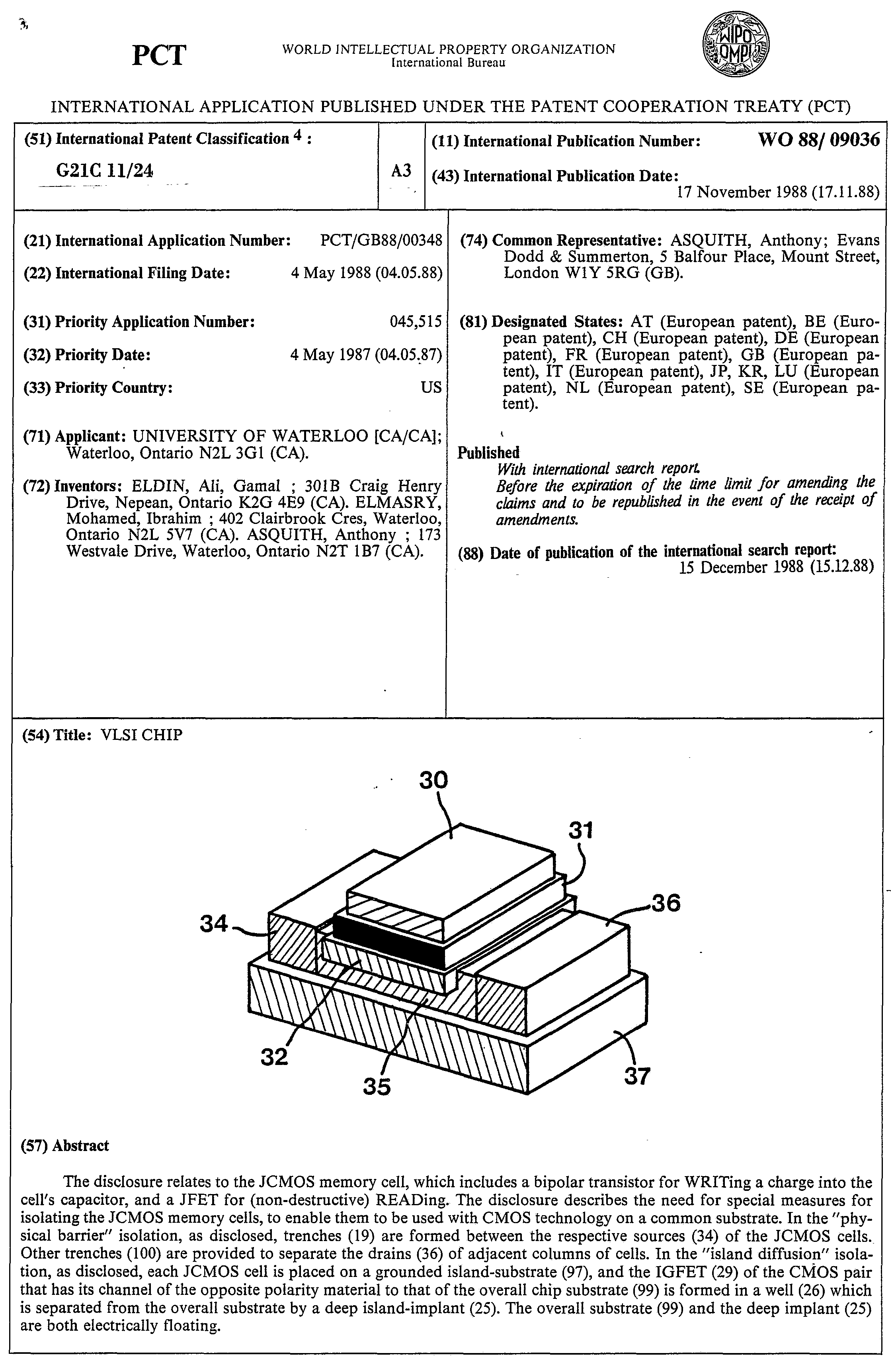
- Fig 1 is a diagram of the the physical layout of a single JCMOS cell.
- the cell includes a p-substrate 37 into which are diffused an n+ source 34 and an n+ drain 36.
- An n-diffused layer 35 constitutes a channel between the source and the drain, and is surmounted by a p-diffused layer 32.
- a layer of oxide 31 (or other insulating material) surmounts the layer 32, and a gate or plate 30 of metal (or other conducting material) resides on top of that.
- the equivalent circuit diagram of the JCMOS cell is shown in Fig 2.
- the regions 30, 31, 32 make up a capacitor, which either does or does not hold a charge, depending on whether the cell is storing a "0" or a "1".
- the regions 32, 35, 37 make up a bipolar transistor, which, when turned on, allows a charge to be placed on, or removed from, the capacitor. Turning on this bipolar transistor therefore allows a WRITE operation to be performed on the cell.
- the regions 34, 35, 36 make up an n-channel junction-gate field-effect transistor.
- the gate of the JFET comprises the bottom plate 32 of the capacitor. This JFET is arranged to either conduct or not conduct depending on whether the capacitor is or is not charged.
- the READ operation is carried out by applying a potential difference between the source 34 and drain 36 of the JFET, and by then sensing whether a current flows through the channel 35 of the JFET.
- Each cell is connected, as shown in Fig 2, to three lines: the WRITE-BIT-LINE 58, the WORD-LINE 50, and the READ-BIT-LINE 53.
- Figs 3A and 3B show several of the cells arranged together on the chip.
- the BIT-LINEs connect the cells together in columns 75,76,78,79 and the WORD-LINEs connect the cells together in rows 71,72,73.
- Fig 3A shows the voltages on the lines during a READ operation.
- Fig 3B shows the same thing during a WRITE operation.
- the cell 74 is the "selected" cell in both cases.
- the READ-BIT-LINEs 53 are connected to sensors, ie to sense-amplifiers, during a READ operation.
- the JFET in the selected JCMOS cell either does or does not conduct a voltage to the respective sense-amplifier on the particular READ-BIT-LINE, depending upon the stored state of the cell.
- Fig 4 shows the arrangement of the sense-amplifier 90 of the column defined by the READ-BIT-LINE 53.
- Each sense-amplifier 90 contains a complementary pair of insulated-gate field-effect transistors 92,93.
- the physical arrangement of these transistors, as diffused onto the chip, is shown in Fig 5.
- Transistor 92 is a p-channel IGFET
- transistor 93 is an n-channel IGFET.
- Also shown in Fig 5 are two of the JCMOS memory cells, one being the "selected" cell 74, and the other being the adjacent cell from the row 78.
- CMOS operation requires that the substrate (in the case of a p-substrate 80) be the most-negative region of the chip, for the following reason.
- the substrate 80 in the case of a p-substrate 80: be the most-negative region of the chip, for the following reason.
- the Source 89 and Drain 87 diffusions cannot be allowed to go negative with respect to the substrate 80, because if that happened the diffusion 87,89 would be forward-biassed with respect to the substrate 80: all the other diffusions in the vicinity are reverse-biassed with respect to the substrate, so that the presence of a forward-biassed diffusion would immediately give rise to a parasitic bipolar transistor action.
- the n-well 86 must never go negative with respect to the substrate 80, for the same reason. Similarly, the p-diffusions comprising the Source 84 and Drain 85 of the p-IGFET 92 should never go positive with respect to the n-well 86.
- CMOS technology normally requires that none of the p-n junctions ever become forward-biassed.
- CMOS technology if a p-type substrate is to be at ground voltage, the designer must see to it that the diffusions can only be connected to voltages that are positive.
- CMOS technology As far as the design of a VLSI memory chip is concerned, the use of CMOS technology is virtually mandatory, because the designer needs the very small energy dissipation feature of a complementary pair of IGFETs.
- the JCMOS memory cell however requires that during the WRITE operation a negative voltage (ie negative with respect to the p-substrate) be connected, via the WORD-LINE 50 to the Source 34 of the selected cell 74. It is this negative voltage which turns on the bipolar transistor of the cell, allowing the capacitor to be charged or discharged.
- the Source 34 of the selected cell (and of all the other cells on the same WORD-LINE) is therefore forward-biassed with respect to the (grounded) substrate 37 during a WRITE operation.
- the JCMOS cell though physically compatible with CMOS technology, is electrically incompatible. If, during a WRITE operation in the JCMOS cell, there were to exist in the vicinity any reverse-biassed n-diffusions, a parasitic bipolar transistor action would immediately ensue - - and in fact, there are of course many such reverse-biassed n-diffusions in the CMOS pairs of IGFETs, which will act as collectors for the electrons emitted from the forward-biassed regions.
- n-type Source 34 when the n-type Source 34 is forward-biassed, there also might occur a parasitic silicon-controlled-rectifier action. This would take place between the following four regions: the n-type Source 34, the p-substrate 37, and the n-well 86 and the p-type Source diffusion 96 of the p-channel IGFET 92.
- a parasitic SCR action if it occurred, could be disastrous to the chip, in that SCR conduction, once established, can become latched into the chip. Again, this possibility of SCR latch-up would seem to indicate that the JCMOS cell is incompatible with CMOS technology.
- the invention is concerned with the recognition that the JCMOS cell can, contrary to these indications, be incorporated into the same chip as IGFETs that are arranged in CMOS complementary pairs.
- the chip is provided with a means for electrically isolating the respective Source diffusion (ie the diffusion connected to the respective WORD-LINE) of each JCMOS cell, at a time when the said diffusion is forward biassed with respect to a second diffusion (being a diffusion of opposite polarity, and contiguous with the Source diffusion) of the chip, from all diffusions on the chip that are contiguous with, and reverse-biassed with respect to, the said second diffusion.
- a means for electrically isolating the respective Source diffusion ie the diffusion connected to the respective WORD-LINE
- a second diffusion being a diffusion of opposite polarity, and contiguous with the Source diffusion
- the JCMOS cell Sources can be electrically isolated from each other by imposing a physical barrier between the Sources, ie a barrier of insulating material.
- the required Isolation can be achieved by forming the JCMOS cells and the CMOS IGFETs in respective island-diffusions, which are allowed to float electrically.
- Fig 6 is a plan view of a section of a chip, showing part of an array of JCMOS memory cells.
- the Sources 5,6,7,8 on any one WORD-LINE 50 are all isolated from the Sources 45,46,47,48, 65,66,67,68 on the other WORD-LINEs 39,51 by the insulators 10.
- Fig 7 is a sectional view along line 7-7 of Fig 6, and Fig 8 is a sectional view along the line 8-8 of Fig 6.
- the insulators 10 comprise Source-separating trenches 19, which are cut (ie etched) or otherwise formed into the depth of the silicon of the chip.
- the trenches are lined with a coating 18 of insulative oxide.
- the trench 19 is filled in with a filler 17 of, for example, polysilicon.
- the filler 17 is just for physical strength; whether the filler is electrically conductive or not is irrelevant.
- the trench 19 should be formed deeply into the material of the chip.
- the trench should be at least as deep, and preferably should be deeper, than the Source diffusions. It may be regarded that the electrons or holes generated by the forward-biassed Sources 5,6,7,8 can reach a reverse-biassed region 45,46,47,48,65,66,67,68 only if the electrons or holes can travel directly in a straight line towards the reverse-biassed region. Thus the deeper the trench 19, the more tortuous the path the electrons or holes are forced to follow to reach a reverse-biassed region.
- Fig 6 shows the layout of the cells as shown in Fig 6 is very efficient as regards the packing density of the cells on the chip.
- the Figure actually shows the components in substantially the correct scale relative to each other, from which it can be seen that it is meaningful to refer to the area of the cell as being made up of a number of square units of area.
- Fig 6 shows four cells A,B,C,D in fourteen squares in the direction parallel to the WORD-LINEs, and five cells J,K,L,M,N in ten squares in the direction of the READ- and WRITE-BIT-LINEs. Each cell therefore requires an area of only seven squares, which is a very efficient utilisation of the space.
- the Drains 69 of the JCMOS cells are connected to each other in rows, as shown in Fig 6, by the respective READ-BIT-LINEs 52,53,54.
- the READ-BIT-LINE itself comprises the n+ diffusion.
- Adjacent READ-BIT-LINEs 52,53 must be electrically insulated, and again isolation trenches 100 are used for this purpose.
- the adjacent READ-LINEs 52,53 are actually diffused as one unitary region, which is then divided into the two READ-LINEs by the Drain-separating trench 100.
- the Sources 5,6 also may be formed as one unitary diffusion, which is then broken up into individual Sources by means of the Source-separating trenches 19.
- Fig 9 shows a JCMOS memory cell formed on an island diffusion 97 of p-type material, the overall substrate 99 of the chip being of n-type material.
- Fig 10 shows a section of the chip in which are located two adjacent pairs of JCMOS cells.
- each pair of cells resides in an individual well 97,98 of p-type material, rather than the whole substrate being of p-type material.
- the cell-substrate 97 is not now unitary with the overall substrate 99 of the chip.
- the substrate 99 itself is of n-type material.
- Fig 11 shows a p-channel IGFET 29 formed in the same n-substrate 99 as is shown in Fig 10.
- the p-type Source 27 and Drain 28 diffusions of the IGFET 29 cannot be allowed to become forward-biassed with respect to the n-substrate 99, so that the n-substrate 99 must be connected to the most positive voltage on the chip.
- the fact that the n-substrate 99 is therefore more positive than the p-well 97 of the JCMOS cell means that the p-well 97 is reverse-biassed with respect to the substrate 99.
- a parasitic bipolar action would occur between the n-substrate 99, the p-well 97 of the memory cell, and the n-Source 5,6 of the memory cell, during a WRITE operation.
- the parasitic bipolar action just described can be prevented by allowing the n-substrate 99 to float electrically, ie by connecting the substrate 99 neither to ground, nor to any other voltage level.
- the floating substrate 99 makes it possible for an SCR latch-up path to exist, between the following regions, ie: the p-type Source 27 of the IGFET 29, which is at positive voltage, the floating n-type substrate 99, the grounded p-well 97, and the n-type Source 5,6 of the JCMOS cell, which, during a WRITE operation, is at negative voltage.
- this parasitic SCR action can be prevented by forming the p-channel IGFET 29 in a well 26 of n-type material, and by surrounding that n-well 26 by a deeper well 25 of p-type material.
- the n-well 26 can be set most-positive, which is compatible with the CMOS technology.
- the deep p-well 25 is allowed to float electrically, like the n-substrate 99.
- JCMOS memory cells may be provided on the same chip as IGFETs arranged in complementary pairs, without the dangers of parasitic bipolar action, nor of SCR latch-up.
- the "island diffusion” means is the more reliable, in that with the "physical barrier” means, there is a slight chance that the electrons/holes that are emitted could find their way around or past the trenches.
- the “island diffusion” means is, in practice, effective to eliminate all spurious bipolar emitters.
- the n- and p-type polarities of the material may be reversed.
Landscapes
- Engineering & Computer Science (AREA)
- Microelectronics & Electronic Packaging (AREA)
- Computer Hardware Design (AREA)
- Power Engineering (AREA)
- Semiconductor Memories (AREA)
- Metal-Oxide And Bipolar Metal-Oxide Semiconductor Integrated Circuits (AREA)
- Dram (AREA)
Abstract
Description
Claims
Applications Claiming Priority (2)
| Application Number | Priority Date | Filing Date | Title |
|---|---|---|---|
| US4551587A | 1987-05-04 | 1987-05-04 | |
| US045,515 | 1987-05-04 |
Publications (2)
| Publication Number | Publication Date |
|---|---|
| WO1988009036A2 true WO1988009036A2 (en) | 1988-11-17 |
| WO1988009036A3 WO1988009036A3 (en) | 1988-12-15 |
Family
ID=21938341
Family Applications (1)
| Application Number | Title | Priority Date | Filing Date |
|---|---|---|---|
| PCT/GB1988/000348 Ceased WO1988009036A2 (en) | 1987-05-04 | 1988-05-04 | Vlsi chip |
Country Status (3)
| Country | Link |
|---|---|
| EP (1) | EP0358668A1 (en) |
| JP (1) | JPH02504335A (en) |
| WO (1) | WO1988009036A2 (en) |
Families Citing this family (2)
| Publication number | Priority date | Publication date | Assignee | Title |
|---|---|---|---|---|
| JPH05129559A (en) * | 1991-09-01 | 1993-05-25 | Tenki Ri | Structure and manufacture of bi-cmos dram cell |
| US6966693B2 (en) * | 2003-01-14 | 2005-11-22 | Hewlett-Packard Development Company, L.P. | Thermal characterization chip |
Family Cites Families (2)
| Publication number | Priority date | Publication date | Assignee | Title |
|---|---|---|---|---|
| US3827034A (en) * | 1972-09-14 | 1974-07-30 | Ferranti Ltd | Semiconductor information storage devices |
| NL7700880A (en) * | 1976-12-17 | 1978-08-01 | Philips Nv | ACCESSIBLE MEMORY WITH JUNCTION FIELD DEFECT TRANSISTORS. |
-
1988
- 1988-05-04 WO PCT/GB1988/000348 patent/WO1988009036A2/en not_active Ceased
- 1988-05-04 JP JP63503845A patent/JPH02504335A/en active Pending
- 1988-05-04 EP EP19880903896 patent/EP0358668A1/en not_active Withdrawn
Also Published As
| Publication number | Publication date |
|---|---|
| JPH02504335A (en) | 1990-12-06 |
| WO1988009036A3 (en) | 1988-12-15 |
| EP0358668A1 (en) | 1990-03-21 |
Similar Documents
| Publication | Publication Date | Title |
|---|---|---|
| US6133597A (en) | Biasing an integrated circuit well with a transistor electrode | |
| JP2950558B2 (en) | Semiconductor device | |
| US5795800A (en) | Integrated circuit fabrication method with buried oxide isolation | |
| US4679171A (en) | MOS/CMOS memory cell | |
| EP1253634A2 (en) | Semiconductor device | |
| US6903419B2 (en) | Semiconductor storage device and semiconductor integrated circuit | |
| US8519462B2 (en) | 6F2 DRAM cell | |
| US6531363B2 (en) | Method for manufacturing a semiconductor integrated circuit of triple well structure | |
| US6136638A (en) | Process technology architecture of embedded DRAM | |
| EP0239187B1 (en) | Semiconductor memory device | |
| KR0181348B1 (en) | Semiconductor device and manufacturing method thereof | |
| JPH0132660B2 (en) | ||
| US4791611A (en) | VLSI dynamic memory | |
| US4364075A (en) | CMOS Dynamic RAM cell and method of fabrication | |
| US10658028B2 (en) | Semiconductor storage device including memory cells, word driver, dummy word driver | |
| WO1988009036A2 (en) | Vlsi chip | |
| JP2003100904A (en) | Semiconductor integrated circuit device and method of manufacturing the same | |
| JP2003060071A (en) | Semiconductor integrated circuit device | |
| US6011712A (en) | Interconnection structures for integrated circuits including recessed conductive layers | |
| US6320233B1 (en) | CMOS semiconductor device | |
| US7250661B2 (en) | Semiconductor memory device with plural source/drain regions | |
| JP2554332B2 (en) | 1-transistor type dynamic memory cell | |
| JPH0752755B2 (en) | Method for manufacturing semiconductor device | |
| US20090067219A1 (en) | Semiconductor memory device including SRAM cell having well power potential supply region provided therein | |
| JPS6115362A (en) | Dynamic ram cell |
Legal Events
| Date | Code | Title | Description |
|---|---|---|---|
| AK | Designated states |
Kind code of ref document: A2 Designated state(s): JP KR |
|
| AL | Designated countries for regional patents |
Kind code of ref document: A2 Designated state(s): AT BE CH DE FR GB IT LU NL SE |
|
| AK | Designated states |
Kind code of ref document: A3 Designated state(s): JP KR |
|
| AL | Designated countries for regional patents |
Kind code of ref document: A3 Designated state(s): AT BE CH DE FR GB IT LU NL SE |
|
| WWE | Wipo information: entry into national phase |
Ref document number: 1988903896 Country of ref document: EP |
|
| WWP | Wipo information: published in national office |
Ref document number: 1988903896 Country of ref document: EP |
|
| WWW | Wipo information: withdrawn in national office |
Ref document number: 1988903896 Country of ref document: EP |