USRE33836E - Apparatus and method for making large area electronic devices, such as flat panel displays and the like, using correlated, aligned dual optical systems - Google Patents
Apparatus and method for making large area electronic devices, such as flat panel displays and the like, using correlated, aligned dual optical systems Download PDFInfo
- Publication number
- USRE33836E USRE33836E US07/573,400 US57340090A USRE33836E US RE33836 E USRE33836 E US RE33836E US 57340090 A US57340090 A US 57340090A US RE33836 E USRE33836 E US RE33836E
- Authority
- US
- United States
- Prior art keywords
- stage
- substrate
- images
- reticle
- image
- Prior art date
- Legal status (The legal status is an assumption and is not a legal conclusion. Google has not performed a legal analysis and makes no representation as to the accuracy of the status listed.)
- Expired - Lifetime
Links
Images


Classifications
-
- G—PHYSICS
- G03—PHOTOGRAPHY; CINEMATOGRAPHY; ANALOGOUS TECHNIQUES USING WAVES OTHER THAN OPTICAL WAVES; ELECTROGRAPHY; HOLOGRAPHY
- G03F—PHOTOMECHANICAL PRODUCTION OF TEXTURED OR PATTERNED SURFACES, e.g. FOR PRINTING, FOR PROCESSING OF SEMICONDUCTOR DEVICES; MATERIALS THEREFOR; ORIGINALS THEREFOR; APPARATUS SPECIALLY ADAPTED THEREFOR
- G03F7/00—Photomechanical, e.g. photolithographic, production of textured or patterned surfaces, e.g. printing surfaces; Materials therefor, e.g. comprising photoresists; Apparatus specially adapted therefor
- G03F7/70—Microphotolithographic exposure; Apparatus therefor
- G03F7/70691—Handling of masks or workpieces
-
- G—PHYSICS
- G03—PHOTOGRAPHY; CINEMATOGRAPHY; ANALOGOUS TECHNIQUES USING WAVES OTHER THAN OPTICAL WAVES; ELECTROGRAPHY; HOLOGRAPHY
- G03F—PHOTOMECHANICAL PRODUCTION OF TEXTURED OR PATTERNED SURFACES, e.g. FOR PRINTING, FOR PROCESSING OF SEMICONDUCTOR DEVICES; MATERIALS THEREFOR; ORIGINALS THEREFOR; APPARATUS SPECIALLY ADAPTED THEREFOR
- G03F7/00—Photomechanical, e.g. photolithographic, production of textured or patterned surfaces, e.g. printing surfaces; Materials therefor, e.g. comprising photoresists; Apparatus specially adapted therefor
- G03F7/70—Microphotolithographic exposure; Apparatus therefor
- G03F7/70216—Mask projection systems
- G03F7/70275—Multiple projection paths, e.g. array of projection systems, microlens projection systems or tandem projection systems
-
- G—PHYSICS
- G03—PHOTOGRAPHY; CINEMATOGRAPHY; ANALOGOUS TECHNIQUES USING WAVES OTHER THAN OPTICAL WAVES; ELECTROGRAPHY; HOLOGRAPHY
- G03F—PHOTOMECHANICAL PRODUCTION OF TEXTURED OR PATTERNED SURFACES, e.g. FOR PRINTING, FOR PROCESSING OF SEMICONDUCTOR DEVICES; MATERIALS THEREFOR; ORIGINALS THEREFOR; APPARATUS SPECIALLY ADAPTED THEREFOR
- G03F7/00—Photomechanical, e.g. photolithographic, production of textured or patterned surfaces, e.g. printing surfaces; Materials therefor, e.g. comprising photoresists; Apparatus specially adapted therefor
- G03F7/70—Microphotolithographic exposure; Apparatus therefor
- G03F7/70425—Imaging strategies, e.g. for increasing throughput or resolution, printing product fields larger than the image field or compensating lithography- or non-lithography errors, e.g. proximity correction, mix-and-match, stitching or double patterning
- G03F7/70475—Stitching, i.e. connecting image fields to produce a device field, the field occupied by a device such as a memory chip, processor chip, CCD, flat panel display
-
- G—PHYSICS
- G03—PHOTOGRAPHY; CINEMATOGRAPHY; ANALOGOUS TECHNIQUES USING WAVES OTHER THAN OPTICAL WAVES; ELECTROGRAPHY; HOLOGRAPHY
- G03F—PHOTOMECHANICAL PRODUCTION OF TEXTURED OR PATTERNED SURFACES, e.g. FOR PRINTING, FOR PROCESSING OF SEMICONDUCTOR DEVICES; MATERIALS THEREFOR; ORIGINALS THEREFOR; APPARATUS SPECIALLY ADAPTED THEREFOR
- G03F7/00—Photomechanical, e.g. photolithographic, production of textured or patterned surfaces, e.g. printing surfaces; Materials therefor, e.g. comprising photoresists; Apparatus specially adapted therefor
- G03F7/70—Microphotolithographic exposure; Apparatus therefor
- G03F7/70691—Handling of masks or workpieces
- G03F7/70791—Large workpieces, e.g. glass substrates for flat panel displays or solar panels
-
- G—PHYSICS
- G03—PHOTOGRAPHY; CINEMATOGRAPHY; ANALOGOUS TECHNIQUES USING WAVES OTHER THAN OPTICAL WAVES; ELECTROGRAPHY; HOLOGRAPHY
- G03F—PHOTOMECHANICAL PRODUCTION OF TEXTURED OR PATTERNED SURFACES, e.g. FOR PRINTING, FOR PROCESSING OF SEMICONDUCTOR DEVICES; MATERIALS THEREFOR; ORIGINALS THEREFOR; APPARATUS SPECIALLY ADAPTED THEREFOR
- G03F7/00—Photomechanical, e.g. photolithographic, production of textured or patterned surfaces, e.g. printing surfaces; Materials therefor, e.g. comprising photoresists; Apparatus specially adapted therefor
- G03F7/70—Microphotolithographic exposure; Apparatus therefor
- G03F7/708—Construction of apparatus, e.g. environment aspects, hygiene aspects or materials
- G03F7/70858—Environment aspects, e.g. pressure of beam-path gas, temperature
- G03F7/70866—Environment aspects, e.g. pressure of beam-path gas, temperature of mask or workpiece
- G03F7/70875—Temperature, e.g. temperature control of masks or workpieces via control of stage temperature
-
- G—PHYSICS
- G03—PHOTOGRAPHY; CINEMATOGRAPHY; ANALOGOUS TECHNIQUES USING WAVES OTHER THAN OPTICAL WAVES; ELECTROGRAPHY; HOLOGRAPHY
- G03F—PHOTOMECHANICAL PRODUCTION OF TEXTURED OR PATTERNED SURFACES, e.g. FOR PRINTING, FOR PROCESSING OF SEMICONDUCTOR DEVICES; MATERIALS THEREFOR; ORIGINALS THEREFOR; APPARATUS SPECIALLY ADAPTED THEREFOR
- G03F7/00—Photomechanical, e.g. photolithographic, production of textured or patterned surfaces, e.g. printing surfaces; Materials therefor, e.g. comprising photoresists; Apparatus specially adapted therefor
- G03F7/70—Microphotolithographic exposure; Apparatus therefor
- G03F7/708—Construction of apparatus, e.g. environment aspects, hygiene aspects or materials
- G03F7/70858—Environment aspects, e.g. pressure of beam-path gas, temperature
- G03F7/70883—Environment aspects, e.g. pressure of beam-path gas, temperature of optical system
- G03F7/70891—Temperature
-
- G—PHYSICS
- G02—OPTICS
- G02F—OPTICAL DEVICES OR ARRANGEMENTS FOR THE CONTROL OF LIGHT BY MODIFICATION OF THE OPTICAL PROPERTIES OF THE MEDIA OF THE ELEMENTS INVOLVED THEREIN; NON-LINEAR OPTICS; FREQUENCY-CHANGING OF LIGHT; OPTICAL LOGIC ELEMENTS; OPTICAL ANALOGUE/DIGITAL CONVERTERS
- G02F1/00—Devices or arrangements for the control of the intensity, colour, phase, polarisation or direction of light arriving from an independent light source, e.g. switching, gating or modulating; Non-linear optics
- G02F1/01—Devices or arrangements for the control of the intensity, colour, phase, polarisation or direction of light arriving from an independent light source, e.g. switching, gating or modulating; Non-linear optics for the control of the intensity, phase, polarisation or colour
- G02F1/13—Devices or arrangements for the control of the intensity, colour, phase, polarisation or direction of light arriving from an independent light source, e.g. switching, gating or modulating; Non-linear optics for the control of the intensity, phase, polarisation or colour based on liquid crystals, e.g. single liquid crystal display cells
- G02F1/133—Constructional arrangements; Operation of liquid crystal cells; Circuit arrangements
- G02F1/136—Liquid crystal cells structurally associated with a semi-conducting layer or substrate, e.g. cells forming part of an integrated circuit
- G02F1/1362—Active matrix addressed cells
- G02F1/13625—Patterning using multi-mask exposure
Definitions
- LAED large area electronic devices
- FPD flat panel displays
- image scanning arrays for facsimile machines or copiers
- print head arrays for facsimile machines or copiers
- FPD's the most commercially advanced of these applications, now measure 4.5 cm ⁇ 6.0 cm, but will soon be as large as 30 cm ⁇ 40 cm. They are typically 2.5 mm thick.
- these devices are formed on a glass substrate, not on single crystal silicon. Each device contains many picture elements (pixels), often made using liquid crystal display (LCD) materials.
- LCD liquid crystal display
- Each pixel is controlled by digital matrix circuitry at the edge of the device, and a thin film transistor (TFT) at each pixel.
- TFT thin film transistor
- the TFT's measure about 5 micrometers (ums) in their smallest horizontal dimension.
- TFT's are multi-layered structures, much like IC's; and the lateral tolerance between vertically-spaced layers must be one micrometer or better.
- Small displays contain typically 100,000 pixels (and TFT's) in one integrated circuit; the largest devices will contain 4,000,000 TFT's.
- This invention is related to wafer stepping, a technique used to make IC's.
- a scaled up wafer stepper will not provide the speed, tolerance, or low production cost required for these large area devices. Performance gains of 5 to 10 ⁇ over current practice are required.
- the intended applications differ from wafer stepping applications in that (a) images must be printed in a controlled manner on unstable, amorphous substrate materials, often transparent glass, (b) there are no "scribe lines" between images; the entire array of images must be oriented and dimensioned to abut, so that the composed array of images functions as one single large area electronic device, (c) the array must be composed of multiple image patterns per layer; up to 9 separate images may be required on one layer (IC's typically use only one pattern per layer), (d) the resulting product is viewed directly by people; therefore, image quality and abutting must meet difficult perception tolerances not relevant in IC manufacture.
- the apparatus and methods of this invention are directed to the rapid creation of precisely aligned layers over large areas of high resolution photoresist images on amorphous substrates, often transparent glass substrates. Significant speed, cost, and alignment tolerance improvements are provided for fabrication of LAED's.
- the large size of substrates used to make LAED's allows one to use two coordinated optical columns, i.e., camera and lens systems, to print the pattern. These two columns, when properly aligned, each print roughly half of an LAED, substantially doubling printing speed over conventional single column steppers since two lenses working simultaneously print twice the area at a time.
- LAED's such as flat panel displays
- All of the individual images must abut to tight horizontal tolerances to form an overall integrated, uniform, and precisely interconnected, correlated circuit pattern, with no perceivable joints. Due to the absence of spacing between images, one normally cannot use an alignment mark between images each time the stage is stepped. Rather, one set of alignment marks for the entire array, placed around the outside edge, is used. As a result, an order of magnitude improvement in stage metrology is needed to maintain vertical alignment tolerances.
- the apparatus of this invention includes special sensor subsystems, appropriate system control software, and machine setup methods to accomplish this improvement.
- the behavior of potentially unstable amorphous substrates must also be corrected for in the apparatus, to achieve proper coordination of the optical columns (cameras) when printing later levels of the LAED pattern.
- the partially completed circuit on the substrate
- the substrate and circuit pattern will likely change in overall size. This "scale” change is measured and compensated for in the system control software, using correcting mechanisms provided in the apparatus.
- the stepper built by Baggaley, et al. imaged a separate plate for each column.
- the relationship among the columns (cameras) was therefore not important; the images from the several columns were never integrated into one contiguous image on one plate.
- the apparatus of our invention must successfully project images in exact spacing, shape, size, and orientation onto one plate, so that an integrated large area electronic device is created from precisely joined images.
- a method for precisely setting and maintaining the absolute column magnification and spacing must be provided.
- Baggaley had no way of repositioning a substrate and no method of adjusting optical columns relative to one another.
- a special six degree of freedom chuck holds the reticle (master object). Motion of this chuck provides for adjustment of magnification, trapezoid error, X, Y position, and rotation of the projected image. The X adjustment also provides for the precise setting of the distance between the two cameras' images.
- Laser interferometer metering of the X and Y stages is used and is referenced to the optical axis of both columns. This enables proper placement of the stage under each optical axis. Stage yaw errors are measured with an extra laser interferometer, and stage yaw is corrected using a special yaw motion built into the Y stage and appropriate control software. In this manner, the substrate is simultaneously positioned in the proper position under the second camera. By correcting for stage yaw in the stage mechanism, the possibility of adding additional columns in the future is simplified.
- An in-stage calibration subsystem is used to establish and maintain the proper correlation between each camera's projected images and the X, Y motion.
- System control software and set-up methods provide proper control of system operations.
- array of images from each of the two lens systems are precisely butted with one another.
- the images from the two lens systems also abut, or almost abut, forming the first layer of a full-size, precise flat panel display.
- a separate, smaller circuit pattern equal to the remainder distance, can be used to fill the intermediate space.
- the column spacing can be fixed, precisely adjusted, yet be unequal to an exact division of the panel size, and still provide significant throughput improvement.
- Each camera also includes a fast, wheel-like reticle changing capability, so that multiple patterns can be printed on one substrate with minimum loss of throughput.
- a variable, rectangular field stop assembly (masking system) is provided. This system allows users to place multiple patterns on one reticle, but print only one pattern at a time. The offset of each such pattern from the optical axis is supplied by the user and compensated for in the control software.
- the round wheel-like changer mechanism carries four reticles, and automatically changes reticles.
- An in-column alignment system quickly positions each reticle after it is interchanged.
- a high-powered mercury arc lamp illuminator provides exposure energy.
- each illuminator is controlled by feedback from an intensity sensor on each lamp. In this manner the exposure energy of each camera can be matched and still provide the proper exposure dose, even though the optical efficiency of each camera may differ. Finally, each camera can be moved up and down on a rigid Z axis, nominally orthogonal to the X, Y plane. This motion provides precise adjustment of focus for each camera, even though the substrate may be at slightly different heights under each camera, due to plate unflatness or stage top runout.
- X and Y laser interferometers reference the right-hand lens column (the lower part of the right-hand camera) to the stage. These two interferometers provide positioning data which is used by the system control computer and software to precisely locate the stage under the right-hand camera.
- a second Y-axis interferometer is provided to measure the horizontal translation error caused by stage yaw.
- a third Y-axis interferometer is provided to maintain yaw control but allows the use of a much shorter stage mirror during some modes of operation.
- a transmission alignment system is included in the X, Y stage, below the substrate.
- a reflective alignment system is mounted on the right-hand lens column above the substrate.
- Calibration data gathered defines a first transfer function for the first level exposure.
- an alignment system either transmission alignment system or reflective alignment system, determines the X, Y location of the substrate, as loaded onto the X, Y stage.
- the rotation of the substrate, and its X, Y scale, are also determined; and the orthogonality between the X and Y axes is measured.
- This new data is used to modify the calibration database of the machine, creating a second transfer function for the second layer, and so on. In this way the apparatus is realigned with the substrate pattern, even when it is placed incorrectly onto the stage, or its amorphous nature has allowed a scale change in either X or Y direction, or both.
- the small differences between machines is automatically corrected for by using this six degree of freedom alignment method.
- the six degrees of freedom for alignment are X-, Y-, plate rotation, X scale, Y scale, and the orthogonality of the X- and Y-axes).
- our apparatus may use additional cameras to provide higher throughput on larger substrates.
- Our system can also be used to create multiple separate circuits upon a single substrate as long as the alignment is set.
- FIG. 1 is an exploded view of a portion of a flat panel display.
- FIG. 2A is an enlarged plan view of a portion of the display of FIG. 1.
- FIG. 2B is a further enlargement of a portion of FIG. 2A.
- FIG. 3 is a section of the thin film transistor, taken on line 3--3 of FIG. 2B.
- FIG. 4 is a plan view of the image layout (viewed from the back of the apparatus as in FIG. 6) required to project abutting images upon a substrate using dual optical columns.
- FIG. 5 is a flow chart explaining the methods for exposing substrates and for handling error calibration.
- FIG. 6 is a rear perspective schematic view showing the optical controls used for aligning the two optical columns with a substrate for producing image patterns such as are shown in FIG. 4.
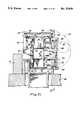
- FIG. 7 is a front elevation of our imaging system showing the stage and the dual optical columns.
- FIG. 8 is top plan view of the imaging system.
- FIG. 9 is a right side elevation of the imaging system.
- FIG. 10 is a rear elevation showing the optical columns and the laser interferometer systems for measurement and calibration.
- FIG. 11 is a plan view of the stage for carrying the substrate and showing the means for moving the stage in x and y directions.
- FIG. 12 is a vertical section taken on line 12--12 of FIG. 11 providing further details of the stage-moving means.
- FIG. 13 is a partial top plan view of the in-stage calibration unit.
- FIG. 14 is a plan view showing the alignment markings and detector geometries of the in-stage calibration unit.
- FIG. 15 is a vertical section taken on line 15--15 of FIG. 13 showing a portion of the in-stage calibration system.
- FIG. 16 is a vertical section taken on line 16--16 of FIG. 14 showing two of the sensors in the in-stage calibration system.
- FIG. 17 is a vertical section taken on line 17--17 of FIG. 8 showing placement of the dual lenses relative to the substrate.
- FIG. 18 is a plan view of the stage showing the transmission alignment system and the ⁇ -drive used for aligning the substrate with the reticles.
- FIG. 19A is a plan view of a portion of a reticle, showing alignment slits.
- FIG. 19B is an illustrative vertical section showing the relationship of the slits of FIG. 19A to the lens and the transmission alignment sensor in the stage.
- FIG. 19C is a plan view of the four sensors in a quadcell detector in the stage and showing the relationship of the four sensors to the slits in the in-stage calibration unit of FIG. 14.
- FIG. 20 is a vertical section, taken on line 20--20 of FIG. 8, showing the optical column and reticle mount for the left-hand camera. It shows the unit as if split in the middle and shown in vertical elevation.
- FIG. 21 is a vertical section (partially broken away) taken on lines 21--21 of FIGS. 8 and 22 of the right-hand reticle changer and field stop assembly.
- FIG. 22 is a side elevation of the reticle carrier and field stop assembly.
- FIG. 23 is a partial top plan view of the camera.
- FIG. 24 is a rear elevation of the left-hand camera.
- FIG. 25 is a side elevation of the camera showing the reticle alignment chuck.
- FIG. 26 is a section taken on line 26--26 of FIG. 25 showing the reticle on the chuck.
- FIG. 27 is a vertical section, partially broken away, taken on line 27--27 of FIG. 7, showing the support system for the right optical column.
- FPD flat panel display 2
- the preparation of a flat panel display 2 involves a new dimension in microlithography.
- the finished product is not a mask, made by repeated printing of the image on a reticle, for a mask is not multi-layered. It is not simply a multi-layered chip, one of a series made on a single wafer, for it is many times the size of a chip, for example, 25 cm on a side. It may be thought of as one large integrated circuit that must be built in parts, in which the parts are created in at least two places on the same substrate simultaneously and must be properly oriented and sized to accurately abut in the completed image. Simultaneous imaging is necessary to provide enhanced throughput time.
- FIG. 1 is an exploded view of a portion of a flat panel display (“FPD”), in this instance a liquid crystal display (“LCD”). It includes five functional layers.
- the first is a white light source 22.
- a first polarizing filter 23A which is usually mounted as a thin film directly on the next component, the circuit plate 19.
- the circuit plate provides electronic control over many small areas, called pixels 10 (see FIGS. 2A and 2B), across the area of the display.
- the next element is the color filter plate 20 which carries the three primary colors, also organized into pixels 10C.
- the back surface of plate 20 is coated with indium tin oxide (“ITO”) to act as a ground plate.
- ITO indium tin oxide
- the last component is another polarizing light filter 23B, rotated 90° with respect to the first
- the sandwich of components described above controls the transmission of light through the display as follows:
- the volume between plates 19 and 20 is filled with liquid crystal material 21.
- This material has the unusual property that it will rotate the polarization of light when an electric field is applied across it between pixel 10 and the ground plate.
- the two polarizing filters cause light coming through that part of the display to be blocked.
- the liquid crystal material 21 at that pixel site rotates the polarized light so that it can pass through the second polarizing filter. In this manner individual pixels of the display are turned on.
- the color of the pixel depends upon the color of its companion pixel on the color filter plate. Colors other than the three primary colors are achieved by "blending" portions of the primary colors. This blending of colors requires that the control of each pixel be proportional, not just on-off, so that various percentages of each primary color can be selected. This property is called “grey scale”.
- each pixel 10 In order to achieve a high resolution color picture each pixel 10 must be small. Many pixels are then used to provide a large area display. For example, one existing LCD display measures about 5.4 cm by 4.6 cm, for a total area of about 24.8 cm. This display uses 90,000 pixels, or about 3630 pixels per square centimeter.
- FIGS. 2A and 2B show enlarged views of a pixel on the circuit plate 19.
- the horizontal gate line 8 is energized (typically, to 20 volts)
- the gates of all transistors 6 in that row are ready to conduct electricity.
- Some of the vertical data lines 9 are energized (typically, to 10 volts), and some data lines are left unenergized.
- the energized data lines cause the transistors 6 at the data and gate line intersections to conduct electrons onto that pixel, turning that pixel on. In normal practice, another row of the display is written periodically.
- the transistors 6 on the inactive rows block the flow of electrons to or from the pixel. This holds the information pattern on each row until it is rewritten on the next scan.
- the nearly constant presence of charge at the "on" pixels gives excellent control of the liquid crystals at those points, resulting in good viewing angle and contrast.
- the transistor at each pixel serves to enhance the quality of the displays.
- the transistors 6 in their corners must be even smaller. Electrical properties also mandate small dimensions for the transistors.
- the transistors are typically made from thin films of amorphous silicon materials, on glass, as shown in FIG. 3. To get acceptable switching speeds from such "low grade" semiconductor materials, small gate lengths must be used, typically they are about 5.0 ums.
- the lateral relationships between vertically spaced image layers is important to circuit tolerances; and usually at least 1.0 um lateral alignment must be achieved. In short, the fabrication of transistors for active matrix displays requires manufacturers to achieve integrated circuit tolerances over the area of a full layer and also between layers.
- Projection aligners can provide the yield and patterning required, but no existing projection system can cover the area of a large display; at best, a 10 to 15 cm area can be printed in one exposure.
- FIG. 6 shows schematically the use of two lens systems 13 and 15 to generate one integrated image on substrate 1, as used in the circuit plate 19 of an active matrix liquid crystal display (AM/LCD).
- A/LCD active matrix liquid crystal display
- An alternative method is to use one camera to step a special reticle image into the remainder space 7, a "remainder image.” (See FIG. 4).
- This remainder image may be designed by the user to exactly fill space 7 a row at a time or may overlap the already projected arrays from each camera, taking advantage of the repetitive nature of the patterns.
- a higher throughput method is to produce reticle artwork for each camera's array that is smaller than the maximum allowed by the lens field of each camera, but is an integer subdivision of the inter-camera spacing. For example, in FIG. 4, if we assume that the optical columns have a minimum spacing 3 (FIG. 6) of 165 mm.
- This remainder space 7 could be filled with a separate 25 mm image, and, here, a fifth stage step for each horizontal row. However, this would require a change of reticle 117, taking approximately 10 seconds.
- a change of reticle 117 taking approximately 10 seconds.
- each single X-direction step can be followed by projection of all images in the Y-direction, followed by the next X-step.
- FIGS. 7-10 and 17 show the stage and the dual optical systems of our imaging system.
- Light for exposure is provided by illuminators 90. This light passes through field stop assembly 121, through the reticle 117, reflects off folding mirror 99, and passes through the main projection lens 13 or 15 to the substrate 1.
- the main projection lens 13 (or 15) images the pattern on reticle 117 onto the substrate 1.
- Use of the folding mirror 99 in the illumination system permits the two lenses to be placed closer to one another than would be the case if the mirrors were absent, since the diameter of the condensing lenses 95 is greater than the diameter of lenses 13 and 15.
- main projection lens 13 or 15
- autofocus sensor 213 FOG. 17
- Z axis drive 105 maintain precise control of focus of the projected image, even when the surface of substrate moves up and down slightly due to material tolerances or stage motion.
- the optical systems 29 rest on a large (1,000 kg) granite bridge structure 75, mounted on legs 77, which in turn are mounted on the large (3,000 kg) granite base 51. This structure provides the rigid, stable platform required for such a large and precise stepping and imaging system.
- Base 51 rests on commercial vibration isolation mounts 53.
- Reticle 117 is held on a six degree of freedom reticle chuck alignment chuck 130.
- Six degree of freedom we mean motion in x-, y-, and z- directions and rotation about ⁇ x , ⁇ y , and ⁇ z axes).
- This chuck's motions permit controlled, programmable motion of reticles as needed to correct magnification, trapezoid error, X, Y, rotation, and inter-image spacing. Since the main projection lenses 13 and 15 are asymmetrical, adjustment of magnification and trapezoid error can be made by varying the lens to reticle distance using actuators 84 and, of focus, by varying the lens to substrate distance. Adjustment of chuck 130 also serves to correlate image spacing and rotation; for example, rotation can be used to align images to compensate for rotation of the substrate.
- stage 11Y is partly mounted upon the X stage 11X, and partly references the main surface of the base 51.
- the X stage provides the Y axis guide 165, and drives the two stages in X. Both stages use commercial, frictionless linear motors 159 and 169 to step the stages across desired distances.
- the Y stage shown in plan view in FIG. 11, contains a banking chuck 189 and vacuum line 190 for drawing substrate 1 against banking pins 187. In this manner, substrates are prealigned on the stages. Provision has been made for substrates as small as 300 mm and as large as 450 mm, square or rectangular.
- the in-stage calibration unit 227 is located under the Y stage, as shown in FIG. 11. This unit is normally kept just below the substrate chucking surface of stage 11Y, but is raised to the image plane 30 when used for calibration of projected images.
- the yaw adjustment mechanism 200 is mounted to the stage 11Y as well.
- Bearings 57 provide the lift support of stage 11Y;
- Y guide bearings 203 and Y guide surface 204 provide guide control for stage 11Y.
- Transmission alignment system units 225A, B, C, D, and E, described below, are placed in the stage, under the edge of substrate 1, where they can be used for transmission alignment of transparent substrates, directly referencing substrate 1, when partly processed, to reticles 117L and 117R.
- Stage positioning is controlled by laser interferometers 17A-17D (FIGS. 6-10).
- Our system uses four interferometers for stage control, one, 17D, for X position, and three in Y, which is not typical.
- Interferometer 17B controls the position of the stage in Y, with reference to reflector 14, mounted on the right hand lens 13, and stage mirror 12Y.
- Interferometer 17C measures the Y translation error under left-hand lens 15 (with reference to reflector 16) caused by stage yaw and, together with the yaw correction mechanism 200, controls stage yaw errors.
- Interferometer 17A is used when the stage travels to its full right position, instead of interferometer 17A, so that stage mirror 12Y can be made shorter and yet provide the full travel in X with active yaw control.
- Stage mirror 12X provides for X position referencing and works in conjunction with interferometer 17D and reflector 18 on lens 13. Both stage mirrors are mounted on stage 11Y and are rigidly connected to substrate 1 during stepping to provide the best possible measurement of the position of substrate 1. (Normally a rotation mechanism for aligning the substrate to the mirrors would be included on top of stage 11Y. However, such rotation mechanisms contribute significantly to measurement errors and decrease stepping speed, so are to be avoided.
- the novel yaw control 200 of this system can be used, as well as chucks 130, to circumvent this problem).
- the entire system is placed in a temperature and particle controlled environmental enclosure (not shown).
- a computer and associated electronics control the system and are housed in separate electronic racks (not shown) outside the environmental enclosure.
- the dual optical systems 29 are mounted on granite bridge 75, above the motions of the machine.
- One optical system is the approximate mirror image of the other, with the exception of mirror 18 and the reflective alignment system 241 which are mounted only on the right-handed camera, on lens 13. The detailed description will therefore only be given for one camera but should be understood to apply to both. Subassemblies will be taken in their order of appearance, proceeding up from substrate 1.
- Each camera contains a main projection lens 13 or 15 (FIGS. 6, 7, 10, 17, and 20).
- This lens is asymmetrical, being telecentric to within 1° on the image (substrate) side and non-telecentric by 10° on the object (reticle) side.
- These values describe the approximate angle of a ray at the edge of the image and object, respectively, where 0° represents a ray that is exactly perpendicular to the image or object planes.
- the tangent of these angles properly predicts image size change with motion along the optical axis. (The tangent of 1° is 0.017).
- magnification stability is achieved, even on inexpensive production substrates.
- the 10° of non-telecentricity equates to 1 um of magnification change across the image field diameter for each 5.7 ums of motion of the reticle 117 in the z-direction with respect to lens 13.
- Non-telecentricity on the object side permits control of magnification.
- This design allows use of a six degree of freedom chuck 130 to adjust magnification of each camera independently and precisely, rather than rely upon having lenses of identical focal length (difficult to achieve within the necessary tolerances).
- Fold mirror 99 folds the optical path so that lenses 13 and 15 can be positioned more closely to one another without the reticle carriers 115, chucks 130, and condensing lenses 95 interfering with one another; and closer lens positioning enhances image accuracy.
- FIG. 23 shows the details of the six degree of freedom reticle chuck 130.
- the entire assembly mounts on support flexures 132 above the main projection lens 13, directly on the lens support 26.
- Three piezoelectric drivers 84 control the distance between the lens and the reticle. These drivers move small distances parallel to the optical axis to correct magnification errors. If any two drivers 84 are driven relative to the third, the tip and tilt ( ⁇ x and ⁇ y ) of the reticle chuck 125 is adjusted. This eliminates trapezoidal error in the imaging system.
- Piezo drives 84 position intermediate frame 140, which supports voice coil drivers 129, 131, and 133, flexure assembly 120, and reticle chuck 125.
- the coil drivers may be of the type disclosed in Borner U.S. Pat. No. 3,569,718).
- Voice coils 129 and 131 move together to adjust the alignment of reticle 117 in the X direction. If they move different amounts, they also serve to adjust alignment in the ⁇ -direction (rotation about the optical axis).
- Coil 133 is used for Y-direction adjustment.
- Each piezoactuator and voice coil contains a local position transducer which enables the control computer to reposition the drive at the correct alignment position (stored in the calibration data base 33DB) after power up or recalibration.
- Reticle carrier 115 shown in FIGS. 7-10, 20-22, and 27, holds four reticles 117 in openings 116.
- carrier 115 is driven by air cylinder 128 toward the reticle (to the left in FIG. 21), moving on slide 122.
- Pneumatic controls turn on vacuum on reticle carrier 115 and release the vacuum in reticle chuck 125. In this manner reticle 117 is passed to carrier 115.
- Air cylinder 128 then returns slide 122 and carrier 115 to the reticle changing position (to the right).
- Reticle carrier drive assembly 124 includes reticle carrier 115 which rotates, driven by motor 123, to place the new reticle in position opposite chuck 125. Carrier 115 is again moved to the left onto locating pin 126. The reticle is then handed off to reticle chuck 125 by reversing the above sequence. In-column alignment reference marks 134, seen in FIG. 27, are then used to precisely align the reticle to the top of the optical column 26.
- a programmable offset is entered into the system calibration database 33DB and is used to offset the alignment of the in-column system the correct amount, re-establishing its proper calibration and alignment.
- the above subsystems, lens 13, mirror 99, six degree of freedom stage 130, and reticle carrier 115 are all mounted on lens support 26, which is connected to camera support 83 by the Z-axis air bearings 106 (FIGS. 23 and 24).
- the Z-axis drive 105 (FIG. 27) supports the whole assembly, and provides Z-axis motions.
- Air cylinder 109 can be used to raise the whole assembly nearly 50 mm, allowing easy exchange of substrates under the lens.
- Fine drive of Z, for automatic correction of focus, is provided by voice coil 112, which drives pivoted support arm 110, mounted on pivot flexures 111. Movement of arm 110 drives lens support 26 through flexure linkages 107 and 108.
- Autofocus is provided by autofocus sensor 213 mounted in close proximity to the bottom of lenses 13 and 15 (FIG. 17).
- the autofocus sensor 213 monitors the distance between the bottom of the lens and the top of the substrate.
- the error signal developed by the sensor is used to drive the Z-axis drive 105.
- the autofocus sensor projects a beam of visible or invisible light (of a frequency that will not affect the photosensitive coating on the substrate) from a light source 215 onto substrate 1 to a point directly under the lens 13 on its optical axis. It is received and reflected back by mirror 218 to the substrate and then to a collector.
- the beam is then collected by the sensor in a manner similar to that in common use on wafer steppers (such as disclosed in Tigreat U.S. Pat. No. 4,447,185).
- the individual focus sensors mounted on each lens allow individual focus of each camera, thereby correcting for substrate and stage height variations that occur between cameras.
- the total panel image can be built up of precisely controlled image pieces that match each other so closely that the subtle differences that remain are invisible to the human eye.
- the spacing between the two cameras is adjustable, so that a standard value of column spacing 3 (FIGS. 4 and 6) (such as our 165.000 mm spacing) can be provided on all machines.
- a differential screw drive is fixed at the front of the right-hand camera to move it in the x-direction; the left-hand camera is considered fixed.
- Bridge support 79 acts as a guiding surface for this motion.
- the two cameras are placed on the bridge in approximate position, a test reticle is aligned on each camera, and the instage calibration unit 227 is used to measure the remaining error in the column spacing 3.
- the differential screw drive is then moved the desired amount, to remove most of the remaining error.
- the motion of the reticle alignment chuck 125 includes enough travel in the X and Y directions to accommodate the remaining adjustment.
- the pop-up calibration unit 227 and the X, Y laser metered stages will be used to locate projected reticle images 5 for each column, as described below. Any error in the exact column spacing can be calculated from the measurement data, and used to offset the reticle alignment origin (stored in the calibration database 33DB) in the direction and amount required to bring the column spacing into exact adjustment. In this manner, the column spacing is set and maintained at an exact value.
- Each reticle may contain more than one image pattern, even though only one is to used at a given time.
- Field stop assembly 121 (FIGS. 7, 8, 21, and 22) is positioned in the optical path between the reticle carrier 115 and the condenser 95. It serves to delineate the portion of a particular reticle that is to be used. Assembly 121 includes a pair of horizontal blades 137, driven by motors 149, guided by ball slide 146, belts 139, and guide slot 148; also, a pair of vertical blades 141, driven by motors 150 guided by ball slide 145, belts 143, and vertical guide slots 147. These blades may form any shape rectangle, providing a field stop for any part of the reticle.
- Assembly 121 is not, and need not be, in the plane of focus of lens 13 or 15 since the patterns on the reticle are spaced and so need not be exactly delineated by the field stop assembly. (A form of assembly is disclosed in Hill U.S. Pat. No. 3,980,407, though the Hill structure, in contrast to ours, only moves symmetrically).
- each optical system 29 includes an illuminator housing 90, which contains a mercury lamp 91, mirrors 93 to direct the light, and exposure control shutter 97, and a condensing lens 95 which directs the light through the field stop assembly 121 to reticle 117 and from there off mirror 99, through lens 13 or 15 onto substrate 1.
- a sensor is included in each illuminator to monitor exposure dose, so that the exposure energy for each system will be the same even when the lamp outputs and the optical efficiencies of the two cameras differ.
- Patterning a 450 mm square area requires a large, and, therefore, heavy stage.
- Aluminum stages weighing nearly 100 kg are used. While the use of two cameras simultaneously can reduce the travel required in one axis by 2X, initial calibration is best accomplished using 450 mm of travel in both X and Y.
- a massive, stiff structure is therefore required to provide rapid stepping and stable optical systems.
- a structure weighing nearly 5,000 kg is used (FIGS. 7-10, 20, and 27).
- Granite base 51 weighing 3,000 kg, rests on commercial vibration isolators 53, which reduces transmission of building vibrations.
- Granite bridge 75 weighs nearly 1,000 kg and supports both optical systems 29. Each optical system, including light source, weighs about 250 kg.
- Legs 77 are stiff enough to maintain high servo-drive bandwidth.
- the roughly 75 kg of assemblies mounted to the lens support casting 26 are supported by Z-axis drives 105. This entire structural assembly provides the stability and stiffness needed to step large stages rapidly, image high resolution patterns, and maintain system calibration.
- X-motion stage 11X moves along the top of base 51, supported on frictionless air bearings 55, and guided by air bearings 158 which move along the X-axis guide keys mounted in a slot in base 51, as shown in FIGS. 7 and 11.
- the guide bearings provide torsional stiffness of the X-axis motion stage 11X. Stiffness of 10,000 kg/mm are needed in these bearings to provide high gain servo control of the combined X and Y axes.
- X-motion stage 11X is driven by a commercial linear motor 159 (FIG. 9).
- the stator 160 for motor 159 consists of two rows of permanent magnets mounted to base 51.
- the armature 161 consists of a set of movable copper coils mounted from the stage so that it is centered between these two rows of magnets. Current in the coils provides thrust to move the stage. Precise control of the current, provided by digital servo loops, fine digital-to-analog converters (DAC's), and linear power amplifiers allows high speed coarse positioning and lower speed fine positioning to 0.10 um with no moving friction parts to wear out or inhibit precise stage positioning. Stops limit the motion of the stage at the ends. This design provides the capability needed to move the heavy stages precisely, without particle contamination, for the more than 20,000,000 steps per year anticipated in high volume production applications.
- the Y guide key 165 is an integral part of the X stage 11X, and provides orthogonal motion guidance for the Y stage 11Y (FIGS. 11 and 12).
- the Y stage is supported on three lift bearings 59. Two of these lift bearings 59 ride directly on the base 51, at the rear of the stage, under mirror 12Y, as can best be seen in FIG. 10.
- the third Y lift bearing 59 rides on top of the X stage. This design allows a 25% reduction of the size and weight of the Y stage, and permits easy service access from the rear.
- Linear motor 169 mounted within the Y guide key 165, provides the drive force to move stage 11Y in the Y direction; stator 171 is mounted to stage 11X, armature 170 is mounted under stage 11Y. Control of motor 169 is the same as described above for the X-axis linear motor 159.
- Interferometers 17 are of the type disclosed in Sommargen U.S. Pat. Nos. 4,688,940 and 4,693,605).
- Interferometer 17D works with stage mirror 12X and mirror 18 mounted on lens 13 to monitor X position.
- Interferometer 17B works with stage mirror 12Y and mirror 14 mounted on the rear of lens 13 to monitor the Y position of the stages relative to the right-hand lens.
- Interferometer 17C works with stage mirror 12Y and mirror 16 mounted on the rear of lens 15 to monitor the Y position of the stage under the left-hand lens.
- interferometer 17B and 17C Due to the nature of X and Y motions, small yaw rotations will occur in the as-built stages. Thus the Y positions determined by interferometers 17B and 17C will differ slightly. The system controls consider the true position to be that measured by interferometer 17B. The difference in distance measurements between the two interferometers represents the error in Y under lens 15 due to stage yaw. If left uncorrected, this error can exceed 1.6 um, which is too large.
- FIG. 18 provides a cutaway view through the Y stage and shows the yaw correcting guide mechanism 200.
- the front two guide bearings 203 are fixed, while the rear two are mounted to lever arms 199. These levers are attached to the Y stage through pivots 201; they are driven by voice coils 197, as shown. Servo current applied to the coils causes the Y stage to rotate slightly, until the yaw error at lens 15 is removed.
- stage 11Y When stage 11Y is moved in X to the far right, see FIG. 10, the laser beam from interferometer 17C will fall off the left end of mirror 12Y.
- the laser beam from interferometer 17C will fall off the left end of mirror 12Y.
- mirror 12Y During normal two camera operation, such travel is not required, and mirror 12Y need not be made longer. However, during initial system calibration the full travel is used. In this case, the mirror 12Y is too short, and active yaw correction is lost.
- a third interferometer 17A is provided to the right of 17B. As can be seen in FIG. 6, the beam from 17A picks up mirror 12Y just before the beam 17C passes off the other end of mirror 12Y.
- stage yaw position is passed by the system controls from interferometer 17C to 17A. In this manner active yaw control is maintained. While interferometer 17A does not reference any optical column, it need not, because in this range of travel, only lens 13 is in a position to image onto the substrate 1, lens 15's optical axis having passed off the left edge of the substrate a approximately the same time as the beam from interferometer 17C passed off mirror 12Y.
- the Y stage carries several sub-assemblies (FIGS. 11 and 18).
- Lift pins 188 are pneumatically driven and lift substrate 1 so that it can be removed from the stage by automatic material handlers. When a substrate is loaded onto the stage, it is placed on top of lift pins 188. These pins then lower the substrate to the stage surface.
- the vacuum line 190 in banking chuck 189 is turned on; the mechanism attached to banking chuck 189, which is below the stage, then pushes substrate 1 gently against banking pins 187 which reference the front and left edge of the substrate, thereby locating substrate 1 in approximate prealignment on top of stage 11Y.
- three or five transmission alignment system units 225A-225E are mounted in the stage under the edge of the substrate. The location of the in-stage calibration unit 227 is also shown.
- Stages 11 provide no separate mechanism for rotating substrate 1 with respect to the stage mirrors. Such mechanisms are common on wafer steppers, but detract from stepping and positioning performance.
- Stage 11Y contains five transmission alignment system sensors, as shown in FIG. 11.
- sensor 225A mounted in the corner
- sensors 225B and 225C will be used for smaller substrates
- sensors 225A, 225D, and 225E will be used for larger substrates, though all five may be used on large substrates. All five sensors are the same; a sectional view of one is shown in FIG. 19.
- Reticle 117 contains transmission alignment system slits 226, as shown in FIG. 19A.
- the surrounding area is opaque; slits 226 are clear, creating small slits of light when shutter 97 is opened.
- Field stop assembly 121 is used to mask all but the transmission alignment system slits of the reticle, so that undesired exposure of the main pattern doesn't take place during transmission alignment system use.
- the light from slits 226 is imaged by lens 13 or 15 onto substrate 1, where a corresponding set of four slits 222 partly blocks the light from the reticle, as shown in FIG. 19B.
- Light passing around substrate slits 222 is gathered by lenses 223 and focused onto quadcell detector 224, as shown.
- FIG. 19C The arrangement of the four detection cells of detector 224 is shown in FIG. 19C.
- the energy from each reticle slit 226 falls separately onto its respective portion of the quad cell detector.
- banking chuck 189 pre-aligns the substrate so that slits 222 fall roughly over transmission alignment system unit 225 at all locations.
- Quad cell detector 224 is large enough so that precise prealignment of substrate 1 to detector 224 is not needed.
- the stage is then moved in X and Y directions until transmission alignment system unit 225 is placed under the image of reticle slit 226 projected by lens 15 from a reticle aligned on the left camera. At this point in the procedure some misalignment will exist.
- slit 226Y1 could fall entirely onto quadcell 224Y1, while slit 226Y2 falls entirely onto the opaque area of substrate 1.
- this imbalance can be detected. It can also be determined which direction of misalignment exists.
- slits 222Y1 and 222Y2 can be moved until they are centered directly under slits 226Y1 and 226Y2.
- the Y position at which this balance is achieved is recorded in the system data base 32DB, as the desired Y location for alignment at location 225A.
- the transmission alignment system directly references projected images at the exposure wavelength. This is the most direct alignment method, and, therefore, the preferred method.
- the transmission alignment system sensors By making the transmission alignment system sensors small, multiple sensors can be easily included around the stage area, thereby avoiding the need for a large hole and viewing microscope intruding up through the stage assembly, as is common on most transmission viewing systems.
- the compactness of the transmission alignment system units is a key to the practical use of transmitted light for alignment.
- the location of the substrate in X, Y and rotation is known from the three position measurements just made. The X length, the Y length, and the angle between X and Y can also be determined. In this manner, six degrees of freedom of alignment of the substrate can be achieved. The use of this data to place the next layer of images correctly over the existing layer(s) is described later.
- a reflective alignment system 241 is provided for such substrates. It is mounted near the bottom of the right lens 13, as shown in FIG. 17. This unit consists of a combined dark field and bright field microscope. A built-in focus sensor is provided to eliminate small, residual non-telecentric effects in the reflective alignment system.
- the image of reflection alignment system mark 228 from the substrate is magnified by this microscope onto a charge coupled device ("CCD") array which is connected to a commercial image processor in the system controls.
- the processor analyzes the magnified image of mark 228 and determines its location in X and Y directions; from this analysis alignment corrections can be determined as above. Again, by measuring the X and Y location of three separate substrate marks, X, Y, ⁇ , scale X, and scale Y alignment can be achieved using the reflective alignment system unit.
- the reflective alignment system unit 241 does not directly reference marks on reticle 117; instead, the CCD array is used as a TV camera and provides an intermediate position reference. As a result, the relationship between reflective alignment system unit 241 and projected reticle images must be separately established during system calibration, and maintained thereafter, even during power downs and restarts.
- An in-stage calibration unit 227 is provided in stage 11Y for this purpose.
- in-stage calibration unit 227 (the "pop-up" unit) is raised by air cylinder 231 to place its top surface, the top surface of glass disc 229, at image plane 30.
- simpler units have been fixed at the image plane, inside the rectangular range of stage travel, but outside the circular area to be patterned (See Johannsmeier U.S. Pat. No. 4,414,749 and Tanimoto U.S. Pat. No. 4,629,313).
- this unused area often doesn't exist; the rectangular substrate may entirely fill the stage area. If such a sensor unit were mounted below the substrate, undesirable Abbe offsets would occur. It is desirable, therefore, to lift the sensor package 227 to the image plane, as shown in FIG. 15.
- Pop-up unit 227 contains three detector subsystems.
- Detector 235 a small light meter, is used to measure the intensity of exposure light coming through lens 13 or 15 at a small portion of the image field. By moving the X and Y stages around the image field of, say, lens 13, the uniformity of intensity of illumination for lens 13 can be determined. Shutter dynamics and exposure dose control behavior can also be measured.
- Detector 237 also contained in the pop-up unit, has two narrow slits, one for the Y-axis and one for the X-axis, aligned with the respective axes. Filtering and detection are provided below the two slits.
- a test reticle which contains an array of similar test slits, is used in conjunction with detector 237. The image of these slits is scanned by the X and Y stages, scanning slit 237Y and then slit 237X across the image of the test slits; during these scans, intensity vs. position data is collected and then analyzed to determine the resolving capability of the lens. If the lens performance is analyzed by stepping the lens along its optical axis, the position of best focus can be determined.
- the desired lens to substrate height is stored in the system calibration data base 33DB, and is then maintained by autofocus systems 213, mounted at the bottom of each lens.
- Pop-up unit 227 also contains a transmission alignment system sensor 230, similar to 225 described above described above. Only now, glass disc 229 carries the transmission alignment system slits 222 normally provided by substrate 1.
- the test reticle contains an array of many transmission alignment system slits 226 placed around the object field. By moving the X, Y stages to the nominal locations of these slits 226 in the projected image, and then making a transmission alignment system alignment at each site, the exact location of the projected images can be determined, as was described above for the transmission alignment system. In this way a map of the projected image errors can be made.
- the system software analyzes this map, using known techniques, to separate X, Y, ⁇ , magnification, and trapezoid errors, and to balance residual distortion errors.
- Sufficient X, Y stage travel is provided so that unit 227 can be scanned under both cameras, across the full image fields of both lenses 13 and 15. In this way, the location of images from both cameras is learned during the calibration procedure, and so is the spacing 3 between cameras.
- the measured X and Y error in camera spacing 3 is then stored in the system calibration database 33DB and is used to offset the right-hand camera's six degrees of freedom reticle alignment chuck 130 the necessary amount to align the two cameras precisely in Y and to space them our preferred 165.000 mm in X.
- the glass disc 229 used with the pop-up unit contains reflective alignment system alignment marks 228 (FIG. 14).
- the X, Y stages place the pop-up unit 227 at the desired location for the reflective alignment system 241, an alignment measurement is made with the reflective alignment system unit. Any error in this alignment is considered an error in the location of the reflective alignment system unit.
- an offset is stored in the system calibration database 32DB and used to correct later alignments. Note that by using an in-stage calibration unit 227 to locate the optical axes for lenses 13 and 15, and to locate the reflective alignment system unit, these three optical axes can be precisely located relative to each other.
- Scale 205 which is used for velocity of light (VOL) correction can be seen in FIG. 17, rigidly mounted on stage mirror 12X.
- Conventional means for measuring the index of refraction of air have at least 1.5 ppm residual errors. Across 450 mm of travel, an error of some 0.68 ums could occur, which is too large. A better means for measuring VOL is needed.
- Prior art reference systems operate only so long as power is not lost; on power up, they provide no absolute reference. (See, for example, Hewlett Packard Technical Data Bulletin on HP 10717A Wavelength Tracker).
- the apparatus of our invention includes scale 205, made of zero expansion material (such as Zerodur) to provide better VOL reference.
- the reflective alignment system unit 241 is used to measure the location of reflective alignment system marks 228B and 228F at the back and front of this scale, respectively.
- the original length which is known, is stored in the system calibration database 32DB.
- this scale is remeasured using the X, Y stages 11 and the reflective alignment system unit 241. Any change in measured length represents a change in VOL from any cause.
- This data is used by the system software to correct the factor used to convert fringe counts into millimeters of travel, as is normal in laser interferometry.
- Changes in focus or magnification of lenses 13 and 15 caused by a change in air index can be compensated for by direct measurement with the in-stage calibration unit 227, or by deduction, in the software, using models for the lens behavior derived from the original lens design modelling. Deductive correction will generally be quicker, therefore preferred.
- adaptive behavior can be included in the software system, whereby the anticipated change is predicted using the deductive models, and is checked using unit 227. The residual errors detected can be used to modify the deductive models until good agreement between these models and actual system performance is achieved.
- Yaw adjustment mechanism 200 and interferometers 17 provide no precise origin for X, Y or ⁇ upon power up.
- Scale 205 serves as the origin for X and Y.
- the reflective alignment system unit 227 is used to measure the X and Y locations of mark 228B, on scale 205. The system software treats this location, then, as the origin of X and Y travel. Reestablishment of the ⁇ origin is covered in the next section.
- the apparatus once assembled out of its component parts, will not, due to the precision required, operate to the desired tolerances. Even if the component parts are built to tight tolerances, this will be true.
- Initial system correction begins with the X, Y stages 11, since all other measurements are referenced to these stages.
- a "perfect" grid plate (with an array of reflective alignment system marks 228 positioned at known distances from one another in X- and Y-directions) is loaded onto stage 11Y. The locations of all these marks is measured with the reflective alignment system 241. Measured differences are assumed to be errors in the X, Y stepping matrix, or "grid" of the machine under test. For example, if the angle between the stage mirrors 11Y and 11X is incorrect by 2.0 arc sec, then 4.5 ums of error will be found across the 450 mm of travel.
- the amount of correction needed to shift the grid until it exactly matches the perfect grid plate is stored in the system's calibration data base 32DB and used to correct subsequent stepping patterns until an exact match has been made to the grid plate. In this manner, precisely matched stepping grids can be achieved on all tools, permitting, if desired, the imaging of successive layers on different tools.
- the grid calibration procedure for the first machine built is more complex than that for successor machines.
- the problem is that no grid standard exists for the size area imaged by our apparatus (450 mm square). So the grid standard for the first tool must be constructed using an iterative method.
- an X, Y array of calibration marks is printed on a substrate.
- the major grid errors can be discovered.
- the matrix of errors so discovered will be entered into the machine's X, Y stage corrections data base 32DB (in FIG.
- the calibrated machine is then used to step an X, Y grid pattern on a 450 mm square Zerodur (thermally stable) plate. This grid plate will record the corrected X and Y grid of the first machine and become the "perfect" grid plate used above.
- test reticles patterned on quartz substrates to tolerances of 0.1 ums (by using commercial IC mask making E-beam tools) are used as the positioning reference at the reticle plane. These test reticles contain transmission alignment system slits 226 (FIGS. 14 and 19) on 10.0000 mm centers, distributed around the 160 mm circular field. Such a test reticle is placed onto each reticle chuck 125 and aligned to the in-column alignment references 134 at the top of each camera.
- Field stop assembly 121 is opened fully; shutters 97 are opened to illuminate the reticles.
- the in-stage calibration unit 227 is then moved to the nominal position of each projected image of each transmission alignment system slit 226 in image plane 30. Deviations from the true position are measured and recorded in the apparatus' calibration data base 33DB. Subsequent analysis (See Holbrook, above) determines the amount of X, Y, ⁇ magnification and trapezoid errors found in each camera's projected images.
- the proper adjustments for the six degree of freedom alignment chucks 130 are calculated (see lens discussion above for an example).
- the calculated adjustments are fed back to each of the six degree of freedom adjustment actuators (described above), so that the desired correction is made. This is again checked by successive measurements, using stage 11 and the in-stage calibration unit 227, until the residual noise level of error is achieved.
- the optical axis position of each camera can be determined from the data as well, and from this data the X and Y separation 3 of the two cameras can be determined.
- the absolute separation is not needed, only the relative separation as compared to the X and Y stage stepping distances.
- the above method determines this desired relationship, by using only one in-stage detector 227 and stepping it around the image field of both lenses with the one stepping grid of stage 11.
- the correction needed in camera separation distance 3 is used to offset the X origin of the right-hand camera's six degree of freedom stage 130.
- both projected images are precisely matched to the grid of the stages, and their separation is precisely set to match the desired 165.000 mm distance of the X-axis of stage 11X travel. This leaves the tool properly corrected and ready for use in making LAED's.
- the second phase of calibration occurs at power up.
- VOL velocity of light
- Each of the actuators in the system contains a small built-in origin sensor, with repositioning capability of roughly 1.0 micron. These sensors serve to reestablish the machine relationships near to the desired, corrected settings.
- all offsets stored in the machine databases 32DB and 33DB are stored on hard disk and, therefore, available upon power up. These are used to offset all actuators by the last measured value. Thus, only one iteration of testing using the grid plate and in-stage calibration unit 227 is required upon power up to restore all corrections. In this way the machine is quickly and easily restored to its corrected performance.
- the third phase of calibration occurs during routine operation, when added corrections may be needed.
- a panel scaling capability may be needed.
- the above calibration assures that the coordinate systems of the two projected images and the X, Y stage coordinate system are aligned with sufficient precision to allow practical integration of their images into panel circuit patterns, such as FPD's.
- subsequent panel process steps may cause the X, Y scale of the panel to change.
- an added layer of aluminum can stress the substrate, causing it to shrink or expand; glass is an amorphous material and will change dimensions significantly as it undergoes temperature cycling in the normal process of depositing and etching panel layers.
- wafer aligners have provided a ⁇ stage just for final rotation adjustment of the substrate, after alignment. On most stepping aligners, this motion is placed between the X, Y stage metrology and the substrate. This extra mechanical linkage causes loss of metrology accuracy and precision, and detracts from throughput, since it is usually a flexible, hence vibrationprone subsystem. It detracts substantially from the accuracy needed for LAED's.
- the apparatus in our invention has eliminated the separate ⁇ stage, and employs instead the ⁇ correction built into the Y axis stage guidance to rotate the entire stage for the ⁇ correction needed.
- the mechanical banking used to pre-align each plate as it is loaded will align plates within 5.0 ums. So only small ⁇ corrections are needed. This precision of prealignment is achievable with panel substrates because they are square or rectangular, not round like wafers, and, because they are large, there is over 30 cm between reference points used for pre-alignment.
- Rotating the stage yaw correction deliberately out of yaw alignment to correct for plate rotation errors is one method by which the panel substrate may be brought into ⁇ alignment.
- Resulting X, Y positioning errors can be calculated from the known yaw rotation command, and entered into the X, Y stage calibration database, as added X, Y offsets. In this way a more rigid, higher throughput, lower cost system design is achieved without decreasing alignment performance.
- An alternate method for correcting substrate 1 misalignment to the X and Y axes is to rotate each camera's six degree of freedom alignment chuck 130 by the measured alignment error angle ⁇ , thereby aligning each image to the orientation of the images on the substrate.
- the X and Y origin for each camera will also need to be adjusted in X and Y by moving chucks 130, so that a line connecting the optical axes of the two cameras is brought into ⁇ alignment as well.
- a "stair-step" stepping pattern will need to be executed, so that the actual stepping pattern of the stages 11 is made parallel to the orientation of the images on the substrate.
- the apparatus and methods described above are controlled by a system computer. All data collection methods and precision adjustments are included in the software and, so, are automatic. This allows the user to repeat the complex calculation procedure quickly and precisely, without a high level of skill. It also allows the user to maximize productive uptime, since complex calibration sequences are handled automatically by the computer.
- the flow chart in FIG. 5 illustrates the use of these procedures during normal operations, such as power up 43, stage corrections 32, camera corrections 33, first level patterning 41, and upper level patterning 42.
- Correction data is stored in data bases 32DB and 33DB for the X, Y motions and the cameras, respectively.
- the data consists of coordinate offsets and scaling coefficients which are used to correct each subsystem so that its operation will be within the desired tolerances. More generally, the data consists of mathematical arrays (matrices).
- Models of subsystem behavior are also kept in these databases.
- the function which describes the nontelecentricity of each lens 13 or 15 is stored in database 33DB and is used to convert a desired magnification change (expressed in %) into motion increment commands (expressed in microns) for drives 84.
- drives 84 are voltage driven devices
- the function that accurately converts motion increment commands (in microns) into volts for drive 84 is also included in the data of database 33DB.
- these functions are known as transfer functions, because they transfer one set of commands into another set, with offset, scale, and unit-of-measure conversions being accomplished in the process. Since the input data is often a matrix of numbers, these transfer functions are also generally expressed as mathematical arrays (matrices).
- Database 32DB contains the correction data and the transfer functions for the X and Y stages.
- the primary input for this database comes from the stage correction procedure 32.
- Information which modifies this database comes from VOL and stage ⁇ origin measurements 38, panel alignment and scale measurements 48, and from real time stage ⁇ control 34.
- Database 33DB contains the correction data and the transfer functions for each camera.
- the primary input for this database comes from the camera correction procedure 33.
- Updates come from reticle selection 45, VOL measurements 38, and autofocus 35.
- All control of the apparatus is accomplished through user interface 39 in the form of job commands, which are then stored in the job command file 40.
- Commands may be typed in via a computer keyboard or may be entered via a programmable touch panel.
- routine operating commands such as "Start”
- An exception is the powerup routines.
- the apparatus Upon powerup, the apparatus automatically executes a set of startup commands that include normal computer diagnostic checks, safety and utility checks, ending with the initialization of each subsystem on the apparatus.
- mark 228B on scale 205 is brought under reflective alignment system unit 241 and its Y-axis location is measured.
- the stages 11 then move the known distance to mark 228F. This distance is calculated from data and functions in database 32DB, namely, the known length of scale 205, and a prior transfer function used to convert interferometer fringe counts into millimeters of motion.
- mark 228F is brought under reflective alignment system unit 241, and the Y-axis location of mark 228F is also determined.
- scale 205 is made of a material such as Zerodur, which does not change its dimension with time or with air pressure, etc., any measured length difference is assumed to be due to a change in air index, due to pressure changes (or any other index changing variable, such as temperature, humidity, etc.).
- the measured error in the length of scale 205 is therefore used to alter the VOL scaling factor in the stage transfer function, so that the computed nominal distance and the actual measured distance from mark 228B to mark 228F become the same.
- process step 38 causes the yaw drive 200 to set the stages to a nominal origin for stage ⁇ (rotation about Z).
- stage ⁇ rotation about Z
- the stages may be at a slightly different ⁇ orientation each time the apparatus is started up. This residual error, however, will be removed by step 33, where the cameras are recalibrated to match the new ⁇ orientation of the stages.
- stage correction procedure 32 may be run. Generally, however, the VOL correction is adequate, assuming that the stages have been corrected once, at some prior date. If, however, the stage correction procedure is to be rerun, one would load a grid calibration plate onto stage 11Y and begin procedure 32.
- Each grid plate contains an array of reflective alignment system marks 228 on a stable substrate, such as Zerodur. The corrected location of each mark on the grid plate is known and is already in database 32DB, from prior calibrations.
- the X and Y stages are moved from mark to mark by stepping the exact distance contained in database 32DB.
- Reflective alignment system unit 241 measures any residual error in the location of each mark. Measured deviations are assumed to be errors in the current X, Y stepping distances. These errors are stored as an array of correction values and become a transfer function, used to modify later commanded stepping distances so that an accurate distance is stepped.
- Procedure 33 the camera correction procedure, uses the X, Y motions as a local measuring machine. The best performance is achieved if the stage correction procedure 32 has been done first, as just described.
- Test reticles 117 which contain an array of transmission alignment system slits 226 on them are loaded onto chucks 125 on each camera and aligned to the in-column alignment references 134.
- the shutter 97 is opened, in-stage calibration unit 227 is raised to image plane 30.
- Sensor 23 is moved around each projected image until the location of the image of each slit 226 is measured. Offset and scale of each projected image can be determined from this process. The distance between each camera is also determined. In this way each camera's projected images are matched to the X, Y stepping distances and angles.
- First level patterns differ from upper level patterns in that first level patterns do not have any pattern on the substrate yet. So no alignment to the substrate is possible.
- the X, Y stages are stepped to each desired exposure location directly, using (see step 46) the transfer function from data base 32DB to modify commanded stepping distances as required by earlier VOL updates (38) and calibration corrections (32). In this manner each exposure is placed in its desired, accurate location.
- each step is increased by +0.4 ums, thereby providing a +2.0 ums correction across the full distance and matching the new stepping pattern exactly to the underlying, expanded pattern.
- the spacing between the optical images must also be adjusted using chuck 130. Since the optical image spacing is generally 165 mm, it must be increased by +1.65 um, which is accomplished by adding an offset to database 33DB, which in turn offsets the origin of the six degree of freedom reticle alignment system 130, so that the proper spacing 3 is provided to exactly match the substrate's new scale. Similarly, the magnification must be adjusted +0.001% so that the 40 mm image being stepped is increased to 40.004 mm to match the new stepping distance.
- the revised databases are used to modify job commands (in our example changing the 40.000 mm stepping distance to 40.004 mm), as the job is executed, again creating a new pattern level which is precisely and accurately matched to the underlying layer(s).
- job commands in our example changing the 40.000 mm stepping distance to 40.004 mm
- the apparatus described herein is maintained in calibration and used to step image arrays with the degree of control required to produce large arrays of electronic devices (such as thin film transistors) on amorphous substrates.
Landscapes
- Physics & Mathematics (AREA)
- General Physics & Mathematics (AREA)
- Health & Medical Sciences (AREA)
- Life Sciences & Earth Sciences (AREA)
- Atmospheric Sciences (AREA)
- Toxicology (AREA)
- Engineering & Computer Science (AREA)
- Environmental & Geological Engineering (AREA)
- Epidemiology (AREA)
- Public Health (AREA)
- Sustainable Development (AREA)
- Exposure And Positioning Against Photoresist Photosensitive Materials (AREA)
Abstract
Description
Claims (67)
Priority Applications (1)
| Application Number | Priority Date | Filing Date | Title |
|---|---|---|---|
| US07/573,400 USRE33836E (en) | 1987-10-22 | 1990-08-24 | Apparatus and method for making large area electronic devices, such as flat panel displays and the like, using correlated, aligned dual optical systems |
Applications Claiming Priority (2)
| Application Number | Priority Date | Filing Date | Title |
|---|---|---|---|
| US07/111,427 US4769680A (en) | 1987-10-22 | 1987-10-22 | Apparatus and method for making large area electronic devices, such as flat panel displays and the like, using correlated, aligned dual optical systems |
| US07/573,400 USRE33836E (en) | 1987-10-22 | 1990-08-24 | Apparatus and method for making large area electronic devices, such as flat panel displays and the like, using correlated, aligned dual optical systems |
Related Parent Applications (1)
| Application Number | Title | Priority Date | Filing Date |
|---|---|---|---|
| US07/111,427 Reissue US4769680A (en) | 1987-10-02 | 1987-10-22 | Apparatus and method for making large area electronic devices, such as flat panel displays and the like, using correlated, aligned dual optical systems |
Publications (1)
| Publication Number | Publication Date |
|---|---|
| USRE33836E true USRE33836E (en) | 1992-03-03 |
Family
ID=26808891
Family Applications (1)
| Application Number | Title | Priority Date | Filing Date |
|---|---|---|---|
| US07/573,400 Expired - Lifetime USRE33836E (en) | 1987-10-22 | 1990-08-24 | Apparatus and method for making large area electronic devices, such as flat panel displays and the like, using correlated, aligned dual optical systems |
Country Status (1)
| Country | Link |
|---|---|
| US (1) | USRE33836E (en) |
Cited By (60)
| Publication number | Priority date | Publication date | Assignee | Title |
|---|---|---|---|---|
| WO1993016394A1 (en) * | 1992-02-18 | 1993-08-19 | Elm Technology Corporation | Stepper scanner discretionary lithography and common mask discretionary lithography for integrated circuits |
| US5264835A (en) * | 1988-07-21 | 1993-11-23 | Proxima Corporation | Enhanced color display system and method of using same |
| US5451489A (en) * | 1988-05-16 | 1995-09-19 | Leedy; Glenn J. | Making and testing an integrated circuit using high density probe points |
| US5512397A (en) * | 1988-05-16 | 1996-04-30 | Leedy; Glenn J. | Stepper scanner discretionary lithography and common mask discretionary lithography for integrated circuits |
| US5625436A (en) * | 1993-11-11 | 1997-04-29 | Nikon Corporation | Scanning type exposure apparatus and exposure method |
| WO1997045827A1 (en) * | 1996-05-28 | 1997-12-04 | The Trustees Of Columbia University In The City Of New York | Crystallization processing of semiconductor film regions on a substrate, and devices made therewith |
| US5812396A (en) * | 1995-03-02 | 1998-09-22 | Canon Kabushiki Kaisha | Synchronous positioning control apparatus and control method thereof |
| US6266144B1 (en) | 1999-08-26 | 2001-07-24 | Taiwan Semiconductor Manufacturing Company | Stepper and scanner new exposure sequence with intra-field correction |
| US6278515B1 (en) * | 2000-08-29 | 2001-08-21 | International Business Machines Corporation | Method and apparatus for adjusting a tilt of a lithography tool |
| US20020005729A1 (en) * | 1988-05-16 | 2002-01-17 | Elm Technology Corporation. | Method and system for probing, testing, burn-in, repairing and programming of integrated circuits in a closed environment using a single apparatus |
| US6341011B1 (en) * | 1997-06-03 | 2002-01-22 | Nikon Corporation | Exposure method |
| US20020101178A1 (en) * | 2000-12-29 | 2002-08-01 | Jae Yong Park | Active matrix organic electroluminescence display device and method for manufacturing the same |
| US6480262B1 (en) | 1993-06-30 | 2002-11-12 | Nikon Corporation | Illumination optical apparatus for illuminating a mask, method of manufacturing and using same, and field stop used therein |
| US20030096489A1 (en) * | 1999-09-03 | 2003-05-22 | Im James S. | Methods for producing uniform large-grained and grain boundary location manipulated polycrystalline thin film semiconductors using sequential lateral solidification |
| US6639740B1 (en) | 2000-08-10 | 2003-10-28 | Nikon Corporation | Catadioptric lens barrel structure having a plurality of split lens barrels and a support structure supporting the split lens barrels |
| US6710754B2 (en) | 2001-11-29 | 2004-03-23 | Palm, Inc. | Moveable output device |
| US20040061843A1 (en) * | 2000-11-27 | 2004-04-01 | Im James S. | Process and mask projection system for laser crystallization processing of semiconductor film regions on a substrate |
| US6856404B2 (en) * | 1998-06-02 | 2005-02-15 | Canon Kabushiki Kaisha | Scanning exposure method and apparatus, and device manufacturing method using the same |
| US20050034653A1 (en) * | 2001-08-27 | 2005-02-17 | James Im | Polycrystalline tft uniformity through microstructure mis-alignment |
| US20050059224A1 (en) * | 2003-09-16 | 2005-03-17 | The Trustees Of Columbia University In The City Of New York | Systems and methods for inducing crystallization of thin films using multiple optical paths |
| US20050056623A1 (en) * | 2003-09-17 | 2005-03-17 | Jung Yun Ho | Sequential lateral solidification device and method of crystallizing silicon using the same |
| US20050059265A1 (en) * | 2003-09-16 | 2005-03-17 | The Trustees Of Columbia University In The City Of New York | Systems and methods for processing thin films |
| US20050059223A1 (en) * | 2003-09-16 | 2005-03-17 | The Trustees Of Columbia University | Laser-irradiated thin films having variable thickness |
| US6894763B2 (en) | 1997-11-22 | 2005-05-17 | Nikon Corporation | Exposure apparatus and methods utilizing plural mask and object stages movable in opposite directions, and methods of producing devices using the same |
| US20050202654A1 (en) * | 2002-08-19 | 2005-09-15 | Im James S. | Process and system for laser crystallization processing of film regions on a substrate to provide substantial uniformity, and a structure of such film regions |
| US20050235903A1 (en) * | 2003-09-19 | 2005-10-27 | The Trustees Of Columbia University In The City Of New York | Single scan irradiation for crystallization of thin films |
| US20050264777A1 (en) * | 2004-05-28 | 2005-12-01 | Azores Corporation | High speed lithography machine and method |
| US20060006464A1 (en) * | 2002-04-01 | 2006-01-12 | Im James S | Method and system for providing a thin film with a controlled crystal orientation using pulsed laser induced melting and nucleation-initiated crystallization |
| US20060040512A1 (en) * | 2002-08-19 | 2006-02-23 | Im James S | Single-shot semiconductor processing system and method having various irradiation patterns |
| US20060060130A1 (en) * | 2002-08-19 | 2006-03-23 | Im James S | Process and system for laser crystallization processing of film regions on a substrate to provide substantial uniformity within arears in such regions and edge areas thereof, and a structure of film regions |
| US20060102901A1 (en) * | 2004-11-18 | 2006-05-18 | The Trustees Of Columbia University In The City Of New York | Systems and methods for creating crystallographic-orientation controlled poly-Silicon films |
| US20060134890A1 (en) * | 2003-02-19 | 2006-06-22 | Im James S | System and process for processing a plurality of semiconductor thin films which are crystallized using sequential lateral solidification techniques |
| US20060148165A1 (en) * | 2003-02-25 | 2006-07-06 | Ui-Jin Chung | Crystallization apparatus and method of amorphous silicon |
| US7115503B2 (en) | 2000-10-10 | 2006-10-03 | The Trustees Of Columbia University In The City Of New York | Method and apparatus for processing thin metal layers |
| US20060254500A1 (en) * | 2005-04-06 | 2006-11-16 | The Trustees Of Columbia University In The City Of New York | Line scan sequential lateral solidification of thin films |
| US20070007242A1 (en) * | 2003-09-16 | 2007-01-11 | The Trustees Of Columbia University In The City Of New York | Method and system for producing crystalline thin films with a uniform crystalline orientation |
| US20070010074A1 (en) * | 2003-09-16 | 2007-01-11 | Im James S | Method and system for facilitating bi-directional growth |
| US20070012664A1 (en) * | 2003-09-16 | 2007-01-18 | Im James S | Enhancing the width of polycrystalline grains with mask |
| US20070020942A1 (en) * | 2003-09-16 | 2007-01-25 | Im James S | Method and system for providing a continuous motion sequential lateral solidification for reducing or eliminating artifacts, and a mask for facilitating such artifact reduction/elimination |
| US20070032096A1 (en) * | 2003-09-16 | 2007-02-08 | Im James S | System and process for providing multiple beam sequential lateral solidification |
| US7220660B2 (en) | 2000-03-21 | 2007-05-22 | The Trustees Of Columbia University In The City Of New York | Surface planarization of thin silicon films during and after processing by the sequential lateral solidification method |
| US20090001523A1 (en) * | 2005-12-05 | 2009-01-01 | Im James S | Systems and Methods for Processing a Film, and Thin Films |
| US20090130795A1 (en) * | 2007-11-21 | 2009-05-21 | Trustees Of Columbia University | Systems and methods for preparation of epitaxially textured thick films |
| US7622370B2 (en) | 2002-08-19 | 2009-11-24 | The Trustees Of Columbia University In The City Of New York | Process and system for laser crystallization processing of film regions on a substrate to minimize edge areas, and a structure of such film regions |
| US20110101368A1 (en) * | 2008-02-29 | 2011-05-05 | The Trustees Of Columbia University In The City Of New York | Flash lamp annealing crystallization for large area thin films |
| US20110108843A1 (en) * | 2007-09-21 | 2011-05-12 | The Trustees Of Columbia University In The City Of New York | Collections of laterally crystallized semiconductor islands for use in thin film transistors |
| US20110121306A1 (en) * | 2009-11-24 | 2011-05-26 | The Trustees Of Columbia University In The City Of New York | Systems and Methods for Non-Periodic Pulse Sequential Lateral Solidification |
| US20110175099A1 (en) * | 2008-02-29 | 2011-07-21 | The Trustees Of Columbia University In The City Of New York | Lithographic method of making uniform crystalline si films |
| US8012861B2 (en) | 2007-11-21 | 2011-09-06 | The Trustees Of Columbia University In The City Of New York | Systems and methods for preparing epitaxially textured polycrystalline films |
| US8415670B2 (en) | 2007-09-25 | 2013-04-09 | The Trustees Of Columbia University In The City Of New York | Methods of producing high uniformity in thin film transistor devices fabricated on laterally crystallized thin films |
| US8426296B2 (en) | 2007-11-21 | 2013-04-23 | The Trustees Of Columbia University In The City Of New York | Systems and methods for preparing epitaxially textured polycrystalline films |
| US8796159B2 (en) | 2003-09-16 | 2014-08-05 | The Trustees Of Columbia University In The City Of New York | Processes and systems for laser crystallization processing of film regions on a substrate utilizing a line-type beam, and structures of such film regions |
| US8802580B2 (en) | 2008-11-14 | 2014-08-12 | The Trustees Of Columbia University In The City Of New York | Systems and methods for the crystallization of thin films |
| US9087696B2 (en) | 2009-11-03 | 2015-07-21 | The Trustees Of Columbia University In The City Of New York | Systems and methods for non-periodic pulse partial melt film processing |
| US9625832B2 (en) | 2012-10-05 | 2017-04-18 | Rudolph Technologies, Inc. | Planar motor system with increased efficiency |
| US9646831B2 (en) | 2009-11-03 | 2017-05-09 | The Trustees Of Columbia University In The City Of New York | Advanced excimer laser annealing for thin films |
| US11215499B1 (en) * | 2019-04-05 | 2022-01-04 | Daedalus Technology Group, Inc. | Calibration apparatus and method |
| US11687010B2 (en) | 2020-02-21 | 2023-06-27 | Onto Innovation Inc. | System and method for correcting overlay errors in a lithographic process |
| US11926911B2 (en) | 2022-02-07 | 2024-03-12 | United States Of America As Represented By The Secretary Of The Air Force | Microfluidic process for the general electrochemical synthesis of geminal dipseudohalide or halide-pseudohalide compounds |
| US12066320B2 (en) | 2019-04-05 | 2024-08-20 | Daedalus Technology Group, Inc. | Calibration system and method |
Citations (18)
| Publication number | Priority date | Publication date | Assignee | Title |
|---|---|---|---|---|
| US3563648A (en) * | 1967-10-18 | 1971-02-16 | Texas Instruments Inc | Step and repeat camera with computer controlled film table |
| US3704945A (en) * | 1971-05-05 | 1972-12-05 | Computervision Corp | Photoplotter accurate film locating mechanism |
| US3722996A (en) * | 1971-01-04 | 1973-03-27 | Electromask Inc | Optical pattern generator or repeating projector or the like |
| US4040736A (en) * | 1973-09-12 | 1977-08-09 | Kasper Instruments, Inc. | Step-and-repeat projection alignment and exposure system |
| JPS59923A (en) * | 1982-06-25 | 1984-01-06 | Toshiba Corp | Projection type light exposing device |
| US4452526A (en) * | 1980-02-29 | 1984-06-05 | Optimetrix Corporation | Step-and-repeat projection alignment and exposure system with auxiliary optical unit |
| JPS60109228A (en) * | 1983-11-18 | 1985-06-14 | Hitachi Ltd | Projection exposing device |
| US4540277A (en) * | 1982-07-09 | 1985-09-10 | Perkin-Elmer Censor Anstalt | Device for the projection printing of masks into a workpiece |
| US4585337A (en) * | 1985-01-14 | 1986-04-29 | Phillips Edward H | Step-and-repeat alignment and exposure system |
| US4620785A (en) * | 1982-12-01 | 1986-11-04 | Canon Kabushiki Kaisha | Sheet-like member having alignment marks and an alignment apparatus for the same |
| US4629313A (en) * | 1982-10-22 | 1986-12-16 | Nippon Kogaku K.K. | Exposure apparatus |
| US4653903A (en) * | 1984-01-24 | 1987-03-31 | Canon Kabushiki Kaisha | Exposure apparatus |
| US4676630A (en) * | 1985-04-25 | 1987-06-30 | Canon Kabushiki Kaisha | Exposure apparatus |
| US4687322A (en) * | 1985-02-12 | 1987-08-18 | Nippon Kogaku K. K. | Projection optical apparatus |
| US4696889A (en) * | 1985-08-23 | 1987-09-29 | Yevick George J | Method of photoforming optical patterns for VLSI devices |
| US4702592A (en) * | 1986-06-30 | 1987-10-27 | Itt Corporation | Reticle assembly, system, and method for using the same |
| US4708466A (en) * | 1986-02-07 | 1987-11-24 | Canon Kabushiki Kaisha | Exposure apparatus |
| US4734746A (en) * | 1985-06-24 | 1988-03-29 | Nippon Kogaku K. K. | Exposure method and system for photolithography |
-
1990
- 1990-08-24 US US07/573,400 patent/USRE33836E/en not_active Expired - Lifetime
Patent Citations (18)
| Publication number | Priority date | Publication date | Assignee | Title |
|---|---|---|---|---|
| US3563648A (en) * | 1967-10-18 | 1971-02-16 | Texas Instruments Inc | Step and repeat camera with computer controlled film table |
| US3722996A (en) * | 1971-01-04 | 1973-03-27 | Electromask Inc | Optical pattern generator or repeating projector or the like |
| US3704945A (en) * | 1971-05-05 | 1972-12-05 | Computervision Corp | Photoplotter accurate film locating mechanism |
| US4040736A (en) * | 1973-09-12 | 1977-08-09 | Kasper Instruments, Inc. | Step-and-repeat projection alignment and exposure system |
| US4452526A (en) * | 1980-02-29 | 1984-06-05 | Optimetrix Corporation | Step-and-repeat projection alignment and exposure system with auxiliary optical unit |
| JPS59923A (en) * | 1982-06-25 | 1984-01-06 | Toshiba Corp | Projection type light exposing device |
| US4540277A (en) * | 1982-07-09 | 1985-09-10 | Perkin-Elmer Censor Anstalt | Device for the projection printing of masks into a workpiece |
| US4629313A (en) * | 1982-10-22 | 1986-12-16 | Nippon Kogaku K.K. | Exposure apparatus |
| US4620785A (en) * | 1982-12-01 | 1986-11-04 | Canon Kabushiki Kaisha | Sheet-like member having alignment marks and an alignment apparatus for the same |
| JPS60109228A (en) * | 1983-11-18 | 1985-06-14 | Hitachi Ltd | Projection exposing device |
| US4653903A (en) * | 1984-01-24 | 1987-03-31 | Canon Kabushiki Kaisha | Exposure apparatus |
| US4585337A (en) * | 1985-01-14 | 1986-04-29 | Phillips Edward H | Step-and-repeat alignment and exposure system |
| US4687322A (en) * | 1985-02-12 | 1987-08-18 | Nippon Kogaku K. K. | Projection optical apparatus |
| US4676630A (en) * | 1985-04-25 | 1987-06-30 | Canon Kabushiki Kaisha | Exposure apparatus |
| US4734746A (en) * | 1985-06-24 | 1988-03-29 | Nippon Kogaku K. K. | Exposure method and system for photolithography |
| US4696889A (en) * | 1985-08-23 | 1987-09-29 | Yevick George J | Method of photoforming optical patterns for VLSI devices |
| US4708466A (en) * | 1986-02-07 | 1987-11-24 | Canon Kabushiki Kaisha | Exposure apparatus |
| US4702592A (en) * | 1986-06-30 | 1987-10-27 | Itt Corporation | Reticle assembly, system, and method for using the same |
Non-Patent Citations (2)
| Title |
|---|
| M. C. King "SPIE Symposium on Microlithography Short Course Notes: Optical Lithography" Mar. 6, 1990, International Society for Optical Engineering, pp. 192-193. |
| M. C. King SPIE Symposium on Microlithography Short Course Notes: Optical Lithography Mar. 6, 1990, International Society for Optical Engineering, pp. 192 193. * |
Cited By (153)
| Publication number | Priority date | Publication date | Assignee | Title |
|---|---|---|---|---|
| US20020005729A1 (en) * | 1988-05-16 | 2002-01-17 | Elm Technology Corporation. | Method and system for probing, testing, burn-in, repairing and programming of integrated circuits in a closed environment using a single apparatus |
| US5451489A (en) * | 1988-05-16 | 1995-09-19 | Leedy; Glenn J. | Making and testing an integrated circuit using high density probe points |
| US5512397A (en) * | 1988-05-16 | 1996-04-30 | Leedy; Glenn J. | Stepper scanner discretionary lithography and common mask discretionary lithography for integrated circuits |
| US20040222809A1 (en) * | 1988-05-16 | 2004-11-11 | Glenn Leedy | System for probing, testing, burn-in, repairing and programming of integrated circuits |
| US5629137A (en) * | 1988-05-16 | 1997-05-13 | Elm Technology Corporation | Method of repairing an integrated circuit structure |
| US5654127A (en) * | 1988-05-16 | 1997-08-05 | Elm Technology Corporation | Method of making a tester surface with high density probe points |
| US6838896B2 (en) | 1988-05-16 | 2005-01-04 | Elm Technology Corporation | Method and system for probing, testing, burn-in, repairing and programming of integrated circuits in a closed environment using a single apparatus |
| US5725995A (en) * | 1988-05-16 | 1998-03-10 | Elm Technology Corporation | Method of repairing defective traces in an integrated circuit structure |
| US6891387B2 (en) | 1988-05-16 | 2005-05-10 | Elm Technology Corporation | System for probing, testing, burn-in, repairing and programming of integrated circuits |
| US5264835A (en) * | 1988-07-21 | 1993-11-23 | Proxima Corporation | Enhanced color display system and method of using same |
| WO1993016394A1 (en) * | 1992-02-18 | 1993-08-19 | Elm Technology Corporation | Stepper scanner discretionary lithography and common mask discretionary lithography for integrated circuits |
| US6480262B1 (en) | 1993-06-30 | 2002-11-12 | Nikon Corporation | Illumination optical apparatus for illuminating a mask, method of manufacturing and using same, and field stop used therein |
| US20030137644A1 (en) * | 1993-06-30 | 2003-07-24 | Nikon Corporation | Exposure apparatus, optical projection apparatus and a method for adjusting the optical projection apparatus |
| US7956984B2 (en) | 1993-06-30 | 2011-06-07 | Nikon Corporation | Exposure apparatus, optical projection apparatus and a method for adjusting the optical projection apparatus |
| US20060238729A1 (en) * | 1993-06-30 | 2006-10-26 | Nikon Corporation | Exposure apparatus, optical projection apparatus and a method for adjusting the optical projection apparatus |
| US20050185162A1 (en) * | 1993-06-30 | 2005-08-25 | Nikon Corporation | Exposure apparatus, optical projection apparatus and a method for adjusting the optical projection apparatus |
| US7023527B2 (en) | 1993-06-30 | 2006-04-04 | Nikon Corporation | Exposure apparatus, optical projection apparatus and a method for adjusting the optical projection apparatus |
| US20080192216A1 (en) * | 1993-06-30 | 2008-08-14 | Nikon Corporation | Exposure apparatus, optical projection apparatus and a method for adjusting the optical projection apparatus |
| US6795169B2 (en) | 1993-06-30 | 2004-09-21 | Nikon Corporation | Exposure apparatus, optical projection apparatus and a method for adjusting the optical projection apparatus |
| US6556278B1 (en) | 1993-06-30 | 2003-04-29 | Nikon Corporation | Exposure/imaging apparatus and method in which imaging characteristics of a projection optical system are adjusted |
| US20050012917A1 (en) * | 1993-06-30 | 2005-01-20 | Nikon Corporation | Exposure apparatus, optical projection apparatus and a method for adjusting the optical projection apparatus |
| US7372544B2 (en) | 1993-06-30 | 2008-05-13 | Nikon Corporation | Exposure apparatus, optical projection apparatus and a method for adjusting the optical projection apparatus |
| US7088425B2 (en) | 1993-06-30 | 2006-08-08 | Nikon Corporation | Exposure apparatus, optical projection apparatus and a method for adjusting the optical projection apparatus |
| US7372543B2 (en) | 1993-06-30 | 2008-05-13 | Nikon Corporation | Exposure apparatus, optical projection apparatus and a method for adjusting the optical projection apparatus |
| USRE37361E1 (en) | 1993-11-11 | 2001-09-11 | Nikon Corporation | Scanning type exposure apparatus and exposure method |
| US5625436A (en) * | 1993-11-11 | 1997-04-29 | Nikon Corporation | Scanning type exposure apparatus and exposure method |
| US5812396A (en) * | 1995-03-02 | 1998-09-22 | Canon Kabushiki Kaisha | Synchronous positioning control apparatus and control method thereof |
| US6322625B2 (en) | 1996-05-28 | 2001-11-27 | The Trustees Of Columbia University In The City Of New York | Crystallization processing of semiconductor film regions on a substrate, and devices made therewith |
| US20100032586A1 (en) * | 1996-05-28 | 2010-02-11 | Im James S | Uniform Large-Grained And Grain Boundary Location Manipulated Polycrystalline Thin Film Semiconductors Formed Using Sequential Lateral Solidification And Devices Formed Thereon |
| WO1997045827A1 (en) * | 1996-05-28 | 1997-12-04 | The Trustees Of Columbia University In The City Of New York | Crystallization processing of semiconductor film regions on a substrate, and devices made therewith |
| US8278659B2 (en) | 1996-05-28 | 2012-10-02 | The Trustees Of Columbia University In The City Of New York | Uniform large-grained and grain boundary location manipulated polycrystalline thin film semiconductors formed using sequential lateral solidification and devices formed thereon |
| US20090173948A1 (en) * | 1996-05-28 | 2009-07-09 | Im James S | Uniform large-grained and grain boundary location manipulated polycrystalline thin film semiconductors formed using sequential lateral solidification and devices formed thereon |
| US7319056B2 (en) | 1996-05-28 | 2008-01-15 | The Trustees Of Columbia University In The City Of New York | Methods for producing uniform large-grained and grain boundary location manipulated polycrystalline thin film semiconductors using sequential lateral solidification |
| US20090189164A1 (en) * | 1996-05-28 | 2009-07-30 | Im James S | Uniform large-grained and grain boundary location manipulated polycrystalline thin film semiconductors formed using sequential lateral solidification and devices formed thereon |
| US8859436B2 (en) | 1996-05-28 | 2014-10-14 | The Trustees Of Columbia University In The City Of New York | Uniform large-grained and grain boundary location manipulated polycrystalline thin film semiconductors formed using sequential lateral solidification and devices formed thereon |
| US8680427B2 (en) | 1996-05-28 | 2014-03-25 | The Trustees Of Columbia University In The City Of New York | Uniform large-grained and gain boundary location manipulated polycrystalline thin film semiconductors formed using sequential lateral solidification and devices formed thereon |
| US7679028B2 (en) | 1996-05-28 | 2010-03-16 | The Trustees Of Columbia University In The City Of New York | Methods for producing uniform large-grained and grain boundary location manipulated polycrystalline thin film semiconductors using sequential lateral solidification |
| US20050255640A1 (en) * | 1996-05-28 | 2005-11-17 | Im James S | Methods for producing uniform large-grained and grain boundary location manipulated polycrystalline thin film semiconductors using sequential lateral solidification |
| US20070202668A1 (en) * | 1996-05-28 | 2007-08-30 | Im James S | Methods for producing uniform large-grained and grain boundary location manipulated polycrystalline thin film semiconductors using sequential laterial solidification |
| US6341011B1 (en) * | 1997-06-03 | 2002-01-22 | Nikon Corporation | Exposure method |
| US6342943B1 (en) | 1997-06-03 | 2002-01-29 | Nikon Corporation | Exposure apparatus |
| US6894763B2 (en) | 1997-11-22 | 2005-05-17 | Nikon Corporation | Exposure apparatus and methods utilizing plural mask and object stages movable in opposite directions, and methods of producing devices using the same |
| US6856404B2 (en) * | 1998-06-02 | 2005-02-15 | Canon Kabushiki Kaisha | Scanning exposure method and apparatus, and device manufacturing method using the same |
| US6266144B1 (en) | 1999-08-26 | 2001-07-24 | Taiwan Semiconductor Manufacturing Company | Stepper and scanner new exposure sequence with intra-field correction |
| US7029996B2 (en) | 1999-09-03 | 2006-04-18 | The Trustees Of Columbia University In The City Of New York | Methods for producing uniform large-grained and grain boundary location manipulated polycrystalline thin film semiconductors using sequential lateral solidification |
| US20030096489A1 (en) * | 1999-09-03 | 2003-05-22 | Im James S. | Methods for producing uniform large-grained and grain boundary location manipulated polycrystalline thin film semiconductors using sequential lateral solidification |
| US20070145017A1 (en) * | 2000-03-21 | 2007-06-28 | The Trustees Of Columbia University | Surface planarization of thin silicon films during and after processing by the sequential lateral solidification method |
| US7220660B2 (en) | 2000-03-21 | 2007-05-22 | The Trustees Of Columbia University In The City Of New York | Surface planarization of thin silicon films during and after processing by the sequential lateral solidification method |
| US7704862B2 (en) | 2000-03-21 | 2010-04-27 | The Trustees Of Columbia University | Surface planarization of thin silicon films during and after processing by the sequential lateral solidification method |
| US6639740B1 (en) | 2000-08-10 | 2003-10-28 | Nikon Corporation | Catadioptric lens barrel structure having a plurality of split lens barrels and a support structure supporting the split lens barrels |
| US6278515B1 (en) * | 2000-08-29 | 2001-08-21 | International Business Machines Corporation | Method and apparatus for adjusting a tilt of a lithography tool |
| US7709378B2 (en) | 2000-10-10 | 2010-05-04 | The Trustees Of Columbia University In The City Of New York | Method and apparatus for processing thin metal layers |
| US7115503B2 (en) | 2000-10-10 | 2006-10-03 | The Trustees Of Columbia University In The City Of New York | Method and apparatus for processing thin metal layers |
| US20090140173A1 (en) * | 2000-10-10 | 2009-06-04 | Im James S | Method and apparatus for processing thin metal layers |
| US6961117B2 (en) | 2000-11-27 | 2005-11-01 | The Trustees Of Columbia University In The City Of New York | Process and mask projection system for laser crystallization processing of semiconductor film regions on a substrate |
| US20040061843A1 (en) * | 2000-11-27 | 2004-04-01 | Im James S. | Process and mask projection system for laser crystallization processing of semiconductor film regions on a substrate |
| US20020101178A1 (en) * | 2000-12-29 | 2002-08-01 | Jae Yong Park | Active matrix organic electroluminescence display device and method for manufacturing the same |
| US6836075B2 (en) | 2000-12-29 | 2004-12-28 | Lg.Philips Lcd Co., Ltd. | Active matrix organic electroluminescence display device and method for manufacturing the same |
| US7285435B2 (en) | 2000-12-29 | 2007-10-23 | Lg.Philips Lcd Co., Ltd. | Active matrix organic electroluminescence display device and method for manufacturing the same |
| US7160763B2 (en) | 2001-08-27 | 2007-01-09 | The Trustees Of Columbia University In The City Of New York | Polycrystalline TFT uniformity through microstructure mis-alignment |
| US20050034653A1 (en) * | 2001-08-27 | 2005-02-17 | James Im | Polycrystalline tft uniformity through microstructure mis-alignment |
| US6710754B2 (en) | 2001-11-29 | 2004-03-23 | Palm, Inc. | Moveable output device |
| US9977641B2 (en) | 2001-11-29 | 2018-05-22 | Qualcomm Incorporated | Display system and method for portable device |
| US20070052617A1 (en) * | 2001-11-29 | 2007-03-08 | Palm, Inc. | Moveable output device |
| US7399359B2 (en) | 2002-04-01 | 2008-07-15 | The Trustees of Columbia University in theCity of New York | Method and system for providing a thin film with a controlled crystal orientation using pulsed laser induced melting and nucleation-initiated crystallization |
| US20060006464A1 (en) * | 2002-04-01 | 2006-01-12 | Im James S | Method and system for providing a thin film with a controlled crystal orientation using pulsed laser induced melting and nucleation-initiated crystallization |
| US7300858B2 (en) | 2002-08-19 | 2007-11-27 | The Trustees Of Columbia University In The City Of New York | Laser crystallization and selective patterning using multiple beamlets |
| US20100065853A1 (en) * | 2002-08-19 | 2010-03-18 | Im James S | Process and system for laser crystallization processing of film regions on a substrate to minimize edge areas, and structure of such film regions |
| US20050202654A1 (en) * | 2002-08-19 | 2005-09-15 | Im James S. | Process and system for laser crystallization processing of film regions on a substrate to provide substantial uniformity, and a structure of such film regions |
| US7622370B2 (en) | 2002-08-19 | 2009-11-24 | The Trustees Of Columbia University In The City Of New York | Process and system for laser crystallization processing of film regions on a substrate to minimize edge areas, and a structure of such film regions |
| US8479681B2 (en) | 2002-08-19 | 2013-07-09 | The Trustees Of Columbia University In The City Of New York | Single-shot semiconductor processing system and method having various irradiation patterns |
| US8411713B2 (en) | 2002-08-19 | 2013-04-02 | The Trustees Of Columbia University In The City Of New York | Process and system for laser crystallization processing of film regions on a substrate to minimize edge areas, and structure of such film regions |
| US8883656B2 (en) | 2002-08-19 | 2014-11-11 | The Trustees Of Columbia University In The City Of New York | Single-shot semiconductor processing system and method having various irradiation patterns |
| US7259081B2 (en) | 2002-08-19 | 2007-08-21 | Im James S | Process and system for laser crystallization processing of film regions on a substrate to provide substantial uniformity, and a structure of such film regions |
| US20060040512A1 (en) * | 2002-08-19 | 2006-02-23 | Im James S | Single-shot semiconductor processing system and method having various irradiation patterns |
| US20110186854A1 (en) * | 2002-08-19 | 2011-08-04 | Im James S | Single-shot semiconductor processing system and method having various irradiation patterns |
| US7718517B2 (en) | 2002-08-19 | 2010-05-18 | Im James S | Single-shot semiconductor processing system and method having various irradiation patterns |
| US20100197147A1 (en) * | 2002-08-19 | 2010-08-05 | Im James S | Single-shot semiconductor processing system and method having various irradiation patterns |
| US7906414B2 (en) | 2002-08-19 | 2011-03-15 | The Trustees Of Columbia University In The City Of New York | Single-shot semiconductor processing system and method having various irradiation patterns |
| US20060060130A1 (en) * | 2002-08-19 | 2006-03-23 | Im James S | Process and system for laser crystallization processing of film regions on a substrate to provide substantial uniformity within arears in such regions and edge areas thereof, and a structure of film regions |
| US7341928B2 (en) | 2003-02-19 | 2008-03-11 | The Trustees Of Columbia University In The City Of New York | System and process for processing a plurality of semiconductor thin films which are crystallized using sequential lateral solidification techniques |
| US20080124526A1 (en) * | 2003-02-19 | 2008-05-29 | Im James S | System and process for processing a plurality of semiconductor thin films which are crystallized using sequential lateral solidification techniques |
| US20060134890A1 (en) * | 2003-02-19 | 2006-06-22 | Im James S | System and process for processing a plurality of semiconductor thin films which are crystallized using sequential lateral solidification techniques |
| US7902052B2 (en) | 2003-02-19 | 2011-03-08 | The Trustees Of Columbia University In The City Of New York | System and process for processing a plurality of semiconductor thin films which are crystallized using sequential lateral solidification techniques |
| US7879700B2 (en) * | 2003-02-25 | 2011-02-01 | Samsung Electronics Co., Ltd. | Crystallization apparatus and method of amorphous silicon |
| US20060148165A1 (en) * | 2003-02-25 | 2006-07-06 | Ui-Jin Chung | Crystallization apparatus and method of amorphous silicon |
| US8063338B2 (en) | 2003-09-16 | 2011-11-22 | The Trustees Of Columbia In The City Of New York | Enhancing the width of polycrystalline grains with mask |
| US20070012664A1 (en) * | 2003-09-16 | 2007-01-18 | Im James S | Enhancing the width of polycrystalline grains with mask |
| US20050059224A1 (en) * | 2003-09-16 | 2005-03-17 | The Trustees Of Columbia University In The City Of New York | Systems and methods for inducing crystallization of thin films using multiple optical paths |
| US9466402B2 (en) | 2003-09-16 | 2016-10-11 | The Trustees Of Columbia University In The City Of New York | Processes and systems for laser crystallization processing of film regions on a substrate utilizing a line-type beam, and structures of such film regions |
| US20050059265A1 (en) * | 2003-09-16 | 2005-03-17 | The Trustees Of Columbia University In The City Of New York | Systems and methods for processing thin films |
| US7638728B2 (en) | 2003-09-16 | 2009-12-29 | The Trustees Of Columbia University In The City Of New York | Enhancing the width of polycrystalline grains with mask |
| US8796159B2 (en) | 2003-09-16 | 2014-08-05 | The Trustees Of Columbia University In The City Of New York | Processes and systems for laser crystallization processing of film regions on a substrate utilizing a line-type beam, and structures of such film regions |
| US8715412B2 (en) | 2003-09-16 | 2014-05-06 | The Trustees Of Columbia University In The City Of New York | Laser-irradiated thin films having variable thickness |
| US20070032096A1 (en) * | 2003-09-16 | 2007-02-08 | Im James S | System and process for providing multiple beam sequential lateral solidification |
| US20070020942A1 (en) * | 2003-09-16 | 2007-01-25 | Im James S | Method and system for providing a continuous motion sequential lateral solidification for reducing or eliminating artifacts, and a mask for facilitating such artifact reduction/elimination |
| US7691687B2 (en) | 2003-09-16 | 2010-04-06 | The Trustees Of Columbia University In The City Of New York | Method for processing laser-irradiated thin films having variable thickness |
| US20050059223A1 (en) * | 2003-09-16 | 2005-03-17 | The Trustees Of Columbia University | Laser-irradiated thin films having variable thickness |
| US20100099273A1 (en) * | 2003-09-16 | 2010-04-22 | The Trustees Of Columbia University In The City Of New York | Enhancing the width of polycrystalline grains with mask |
| US8663387B2 (en) | 2003-09-16 | 2014-03-04 | The Trustees Of Columbia University In The City Of New York | Method and system for facilitating bi-directional growth |
| US7164152B2 (en) | 2003-09-16 | 2007-01-16 | The Trustees Of Columbia University In The City Of New York | Laser-irradiated thin films having variable thickness |
| US20070010074A1 (en) * | 2003-09-16 | 2007-01-11 | Im James S | Method and system for facilitating bi-directional growth |
| US7759230B2 (en) | 2003-09-16 | 2010-07-20 | The Trustees Of Columbia University In The City Of New York | System for providing a continuous motion sequential lateral solidification for reducing or eliminating artifacts in overlap regions, and a mask for facilitating such artifact reduction/elimination |
| US8476144B2 (en) | 2003-09-16 | 2013-07-02 | The Trustees Of Columbia University In The City Of New York | Method for providing a continuous motion sequential lateral solidification for reducing or eliminating artifacts in edge regions, and a mask for facilitating such artifact reduction/elimination |
| US20070007242A1 (en) * | 2003-09-16 | 2007-01-11 | The Trustees Of Columbia University In The City Of New York | Method and system for producing crystalline thin films with a uniform crystalline orientation |
| US20100233888A1 (en) * | 2003-09-16 | 2010-09-16 | Im James S | Method And System For Providing A Continuous Motion Sequential Lateral Solidification For Reducing Or Eliminating Artifacts In Edge Regions, And A Mask For Facilitating Such Artifact Reduction/Elimination |
| US7364952B2 (en) | 2003-09-16 | 2008-04-29 | The Trustees Of Columbia University In The City Of New York | Systems and methods for processing thin films |
| US20100187529A1 (en) * | 2003-09-16 | 2010-07-29 | Columbia University | Laser-irradiated thin films having variable thickness |
| US7318866B2 (en) | 2003-09-16 | 2008-01-15 | The Trustees Of Columbia University In The City Of New York | Systems and methods for inducing crystallization of thin films using multiple optical paths |
| US20070111349A1 (en) * | 2003-09-16 | 2007-05-17 | James Im | Laser-irradiated thin films having variable thickness |
| US8034698B2 (en) | 2003-09-16 | 2011-10-11 | The Trustees Of Columbia University In The City Of New York | Systems and methods for inducing crystallization of thin films using multiple optical paths |
| US20090045181A1 (en) * | 2003-09-16 | 2009-02-19 | The Trustees Of Columbia University In The City Of New York | Systems and methods for processing thin films |
| CN100338521C (en) * | 2003-09-17 | 2007-09-19 | Lg.菲利浦Lcd株式会社 | Sequential lateral solidification device and method of crystallizing silicon using the same |
| US7700892B2 (en) * | 2003-09-17 | 2010-04-20 | Lg Display Co., Ltd. | Sequential lateral solidification device and method of crystallizing silicon using the same |
| US20050056623A1 (en) * | 2003-09-17 | 2005-03-17 | Jung Yun Ho | Sequential lateral solidification device and method of crystallizing silicon using the same |
| US7311778B2 (en) | 2003-09-19 | 2007-12-25 | The Trustees Of Columbia University In The City Of New York | Single scan irradiation for crystallization of thin films |
| US8445365B2 (en) | 2003-09-19 | 2013-05-21 | The Trustees Of Columbia University In The City Of New York | Single scan irradiation for crystallization of thin films |
| US20050235903A1 (en) * | 2003-09-19 | 2005-10-27 | The Trustees Of Columbia University In The City Of New York | Single scan irradiation for crystallization of thin films |
| US7964480B2 (en) | 2003-09-19 | 2011-06-21 | Trustees Of Columbia University In The City Of New York | Single scan irradiation for crystallization of thin films |
| US20050264777A1 (en) * | 2004-05-28 | 2005-12-01 | Azores Corporation | High speed lithography machine and method |
| US7385671B2 (en) | 2004-05-28 | 2008-06-10 | Azores Corporation | High speed lithography machine and method |
| US8734584B2 (en) | 2004-11-18 | 2014-05-27 | The Trustees Of Columbia University In The City Of New York | Systems and methods for creating crystallographic-orientation controlled poly-silicon films |
| US20090309104A1 (en) * | 2004-11-18 | 2009-12-17 | Columbia University | SYSTEMS AND METHODS FOR CREATING CRYSTALLOGRAPHIC-ORIENTATION CONTROLLED poly-SILICON FILMS |
| US20060102901A1 (en) * | 2004-11-18 | 2006-05-18 | The Trustees Of Columbia University In The City Of New York | Systems and methods for creating crystallographic-orientation controlled poly-Silicon films |
| US7645337B2 (en) | 2004-11-18 | 2010-01-12 | The Trustees Of Columbia University In The City Of New York | Systems and methods for creating crystallographic-orientation controlled poly-silicon films |
| US8617313B2 (en) | 2005-04-06 | 2013-12-31 | The Trustees Of Columbia University In The City Of New York | Line scan sequential lateral solidification of thin films |
| US8221544B2 (en) | 2005-04-06 | 2012-07-17 | The Trustees Of Columbia University In The City Of New York | Line scan sequential lateral solidification of thin films |
| US20060254500A1 (en) * | 2005-04-06 | 2006-11-16 | The Trustees Of Columbia University In The City Of New York | Line scan sequential lateral solidification of thin films |
| US8598588B2 (en) | 2005-12-05 | 2013-12-03 | The Trustees Of Columbia University In The City Of New York | Systems and methods for processing a film, and thin films |
| US20090001523A1 (en) * | 2005-12-05 | 2009-01-01 | Im James S | Systems and Methods for Processing a Film, and Thin Films |
| US20110108843A1 (en) * | 2007-09-21 | 2011-05-12 | The Trustees Of Columbia University In The City Of New York | Collections of laterally crystallized semiconductor islands for use in thin film transistors |
| US9012309B2 (en) | 2007-09-21 | 2015-04-21 | The Trustees Of Columbia University In The City Of New York | Collections of laterally crystallized semiconductor islands for use in thin film transistors |
| US8614471B2 (en) | 2007-09-21 | 2013-12-24 | The Trustees Of Columbia University In The City Of New York | Collections of laterally crystallized semiconductor islands for use in thin film transistors |
| US8415670B2 (en) | 2007-09-25 | 2013-04-09 | The Trustees Of Columbia University In The City Of New York | Methods of producing high uniformity in thin film transistor devices fabricated on laterally crystallized thin films |
| US20090130795A1 (en) * | 2007-11-21 | 2009-05-21 | Trustees Of Columbia University | Systems and methods for preparation of epitaxially textured thick films |
| US8012861B2 (en) | 2007-11-21 | 2011-09-06 | The Trustees Of Columbia University In The City Of New York | Systems and methods for preparing epitaxially textured polycrystalline films |
| US8426296B2 (en) | 2007-11-21 | 2013-04-23 | The Trustees Of Columbia University In The City Of New York | Systems and methods for preparing epitaxially textured polycrystalline films |
| US8557040B2 (en) | 2007-11-21 | 2013-10-15 | The Trustees Of Columbia University In The City Of New York | Systems and methods for preparation of epitaxially textured thick films |
| US8871022B2 (en) | 2007-11-21 | 2014-10-28 | The Trustees Of Columbia University In The City Of New York | Systems and methods for preparation of epitaxially textured thick films |
| US20110101368A1 (en) * | 2008-02-29 | 2011-05-05 | The Trustees Of Columbia University In The City Of New York | Flash lamp annealing crystallization for large area thin films |
| US20110175099A1 (en) * | 2008-02-29 | 2011-07-21 | The Trustees Of Columbia University In The City Of New York | Lithographic method of making uniform crystalline si films |
| US8569155B2 (en) | 2008-02-29 | 2013-10-29 | The Trustees Of Columbia University In The City Of New York | Flash lamp annealing crystallization for large area thin films |
| US8802580B2 (en) | 2008-11-14 | 2014-08-12 | The Trustees Of Columbia University In The City Of New York | Systems and methods for the crystallization of thin films |
| US9087696B2 (en) | 2009-11-03 | 2015-07-21 | The Trustees Of Columbia University In The City Of New York | Systems and methods for non-periodic pulse partial melt film processing |
| US9646831B2 (en) | 2009-11-03 | 2017-05-09 | The Trustees Of Columbia University In The City Of New York | Advanced excimer laser annealing for thin films |
| US20110121306A1 (en) * | 2009-11-24 | 2011-05-26 | The Trustees Of Columbia University In The City Of New York | Systems and Methods for Non-Periodic Pulse Sequential Lateral Solidification |
| US8889569B2 (en) | 2009-11-24 | 2014-11-18 | The Trustees Of Columbia University In The City Of New York | Systems and methods for non-periodic pulse sequential lateral soldification |
| US8440581B2 (en) | 2009-11-24 | 2013-05-14 | The Trustees Of Columbia University In The City Of New York | Systems and methods for non-periodic pulse sequential lateral solidification |
| US9625832B2 (en) | 2012-10-05 | 2017-04-18 | Rudolph Technologies, Inc. | Planar motor system with increased efficiency |
| US11215499B1 (en) * | 2019-04-05 | 2022-01-04 | Daedalus Technology Group, Inc. | Calibration apparatus and method |
| US12066320B2 (en) | 2019-04-05 | 2024-08-20 | Daedalus Technology Group, Inc. | Calibration system and method |
| US11687010B2 (en) | 2020-02-21 | 2023-06-27 | Onto Innovation Inc. | System and method for correcting overlay errors in a lithographic process |
| US11926911B2 (en) | 2022-02-07 | 2024-03-12 | United States Of America As Represented By The Secretary Of The Air Force | Microfluidic process for the general electrochemical synthesis of geminal dipseudohalide or halide-pseudohalide compounds |
Similar Documents
| Publication | Publication Date | Title |
|---|---|---|
| USRE33836E (en) | Apparatus and method for making large area electronic devices, such as flat panel displays and the like, using correlated, aligned dual optical systems | |
| US4769680A (en) | Apparatus and method for making large area electronic devices, such as flat panel displays and the like, using correlated, aligned dual optical systems | |
| US5811211A (en) | Peripheral edge exposure method | |
| JP2679186B2 (en) | Exposure equipment | |
| US6333776B1 (en) | Projection exposure apparatus | |
| JP2690960B2 (en) | Magnification projection exposure method and apparatus | |
| US4999669A (en) | Levelling device in an exposure apparatus | |
| KR101240130B1 (en) | Exposure device, exposure method, and micro device manufacturing method | |
| US6337162B1 (en) | Method of exposure, photomask, method of production of photomask, microdevice, and method of production of microdevice | |
| US7385671B2 (en) | High speed lithography machine and method | |
| US4708465A (en) | Exposure apparatus | |
| CN101957567A (en) | The position correction of the alignment head in the bull alignment system | |
| CN102890431B (en) | Exposure method and device and manufacturing method | |
| JP4273679B2 (en) | Split sequential proximity exposure system | |
| US6172740B1 (en) | Projection exposure apparatus and device manufacturing method | |
| US5150152A (en) | Exposure apparatus including device for determining movement of an object | |
| JPS62122215A (en) | Projection-exposure equipment | |
| US20040025322A1 (en) | Waffle wafer chuck apparatus and method | |
| JP2010087310A (en) | Exposure apparatus, and method of manufacturing device | |
| JPH06232027A (en) | Projection aligner | |
| JP2000228344A (en) | Scanning projection aligner and device-manufacturing method | |
| JPH10294257A (en) | Method and apparatus for control of face position of substrate as well as method and apparatus for exposure | |
| JPH11219999A (en) | Delivery method for substrate and aligner using the same | |
| US20070024938A1 (en) | Method and apparatus using hologram masks for printing composite patterns onto large substrates | |
| US10474041B1 (en) | Digital lithography with extended depth of focus |
Legal Events
| Date | Code | Title | Description |
|---|---|---|---|
| AS | Assignment |
Owner name: FLEET BANK OF MASSACHUSETTS, N.W. Free format text: SECURITY INTEREST;ASSIGNOR:MRS TECHNOLOGY, INC.;REEL/FRAME:006589/0688 Effective date: 19930506 |
|
| AS | Assignment |
Owner name: MRS TECHNOLOGY, INC., MASSACHUSETTS Free format text: RELEASE BY SECURED PARTY;ASSIGNOR:FLEET BANK OF MASSACHUSETTS, N.A.;REEL/FRAME:006767/0666 Effective date: 19931022 |
|
| FEPP | Fee payment procedure |
Free format text: PAT HOLDER CLAIMS SMALL ENTITY STATUS - SMALL BUSINESS (ORIGINAL EVENT CODE: SM02); ENTITY STATUS OF PATENT OWNER: SMALL ENTITY |
|
| FPAY | Fee payment |
Year of fee payment: 8 |
|
| FPAY | Fee payment |
Year of fee payment: 12 |
|
| AS | Assignment |
Owner name: AZORES CORPORATION, MASSACHUSETTS Free format text: SALE PURSUANT TO BANKRUPTCY;ASSIGNOR:COAST BUSINESS CREDIT;REEL/FRAME:010881/0882 Effective date: 19990412 |
|
| AS | Assignment |
Owner name: COAST BUSINESS CREDIT, CALIFORNIA Free format text: STATE OF MASS FORM UCC-1; MOTION OF ENTRY OF ORDER TO TERMINATE AUTOMATIC STAY; PROCEEDING MEMORANDUM/ORDER OF COURT; AND TRANSMITTAL OF TITLE TRANSFER DOCUMENTS;ASSIGNOR:MRS TECHNOLOGY, INC.;REEL/FRAME:014154/0300 Effective date: 19990218 |
|
| AS | Assignment |
Owner name: RUDOLPH TECHNOLOGIES, INC., NEW JERSEY Free format text: NUNC PRO TUNC ASSIGNMENT;ASSIGNOR:AZORES CORPORATION;REEL/FRAME:030207/0009 Effective date: 20130207 |