US9953692B1 - Spin orbit torque MRAM memory cell with enhanced thermal stability - Google Patents
Spin orbit torque MRAM memory cell with enhanced thermal stability Download PDFInfo
- Publication number
- US9953692B1 US9953692B1 US15/485,049 US201715485049A US9953692B1 US 9953692 B1 US9953692 B1 US 9953692B1 US 201715485049 A US201715485049 A US 201715485049A US 9953692 B1 US9953692 B1 US 9953692B1
- Authority
- US
- United States
- Prior art keywords
- layer
- antiferromagnetic
- memory cell
- tunnel junction
- magnetic tunnel
- Prior art date
- Legal status (The legal status is an assumption and is not a legal conclusion. Google has not performed a legal analysis and makes no representation as to the accuracy of the status listed.)
- Active
Links
Images


Classifications
-
- G—PHYSICS
- G11—INFORMATION STORAGE
- G11C—STATIC STORES
- G11C11/00—Digital stores characterised by the use of particular electric or magnetic storage elements; Storage elements therefor
- G11C11/02—Digital stores characterised by the use of particular electric or magnetic storage elements; Storage elements therefor using magnetic elements
- G11C11/16—Digital stores characterised by the use of particular electric or magnetic storage elements; Storage elements therefor using magnetic elements using elements in which the storage effect is based on magnetic spin effect
- G11C11/165—Auxiliary circuits
- G11C11/1675—Writing or programming circuits or methods
-
- G—PHYSICS
- G11—INFORMATION STORAGE
- G11C—STATIC STORES
- G11C11/00—Digital stores characterised by the use of particular electric or magnetic storage elements; Storage elements therefor
- G11C11/02—Digital stores characterised by the use of particular electric or magnetic storage elements; Storage elements therefor using magnetic elements
- G11C11/16—Digital stores characterised by the use of particular electric or magnetic storage elements; Storage elements therefor using magnetic elements using elements in which the storage effect is based on magnetic spin effect
- G11C11/161—Digital stores characterised by the use of particular electric or magnetic storage elements; Storage elements therefor using magnetic elements using elements in which the storage effect is based on magnetic spin effect details concerning the memory cell structure, e.g. the layers of the ferromagnetic memory cell
-
- H01L43/08—
-
- H01L43/10—
-
- H—ELECTRICITY
- H10—SEMICONDUCTOR DEVICES; ELECTRIC SOLID-STATE DEVICES NOT OTHERWISE PROVIDED FOR
- H10N—ELECTRIC SOLID-STATE DEVICES NOT OTHERWISE PROVIDED FOR
- H10N50/00—Galvanomagnetic devices
- H10N50/10—Magnetoresistive devices
-
- H—ELECTRICITY
- H10—SEMICONDUCTOR DEVICES; ELECTRIC SOLID-STATE DEVICES NOT OTHERWISE PROVIDED FOR
- H10N—ELECTRIC SOLID-STATE DEVICES NOT OTHERWISE PROVIDED FOR
- H10N52/00—Hall-effect devices
Definitions
- Memory is widely used in various electronic devices such as cellular telephones, digital cameras, personal digital assistants, medical electronics, mobile computing devices, non-mobile computing devices and data servers.
- Memory may comprise non-volatile memory or volatile memory.
- a non-volatile memory allows information to be stored and retained even when the non-volatile memory is not connected to a source of power (e.g., a battery).
- MRAM magnetoresistive random access memory
- MRAM uses magnetization to represent stored data, in contrast to other memory technologies that use electronic charges to store data.
- MRAM includes a large number of magnetic memory cells formed on a semiconductor substrate, where each memory cell represents one data bit. A bit of data is written to a memory cell by changing the direction of magnetization of a magnetic element within the memory cell, and a bit is read by measuring the resistance of the memory cell (e.g., low resistance typically represents a “0” bit and high resistance typically represents a “1” bit).
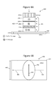
- FIG. 1A is a schematic perspective view of an example prior art MRAM memory cell 100 that makes use of spin orbit torque (SOT) for switching.
- SHE spin Hall Effect
- Memory cell 100 includes three terminals A, B and C; magnetic tunnel junction (MTJ) 101 ; and SHE layer 120 .
- MTJ 101 comprises pinned layer (PL) 102 , inter-layer coupling (ILC) layer 104 , reference layer (RL) 106 , tunnel barrier (TB) 108 and free layer (FL) 110 .
- free layer (FL) 110 has a direction of magnetization that can be switched between INTO the page and OUT of the page.
- a write current 122 is applied between terminal B and terminal C. Reading is achieved by passing current between terminal A and terminal B in order to sense the resistance of memory cell 100 . If the direction of magnetization of free layer (FL) 110 is parallel to the direction of magnetization of the RL ( 106 ), for example INTO the page, then memory cell 100 has a lower resistance. If the direction of magnetization of free layer (FL) 110 is antiparallel to the direction of magnetization of the RL ( 106 ), for example OUT the page, then memory cell 100 has a higher resistance.
- FIG. 1B is a top view of memory cell 100 , with bidirectional arrow 130 indicating the switchable direction of magnetization of free layer 110 .
- the shape of MTJ 101 is elliptical in order to maintain thermal stability. Namely, the elliptical shape of the FL introduces magnetic shape anisotropy which provides energy barrier against thermally activated magnetization reversal of the FL thus making FL magnetization thermally stable.
- the shape of SHE layer 120 is rectangular.
- the primary advantage of the SOT-switching design that exploits the SHE is that the write current 122 passes solely through the SHE layer 120 , and does not flow through the tunnel barrier 108 . This avoids long term degradation of the tunnel barrier by the switching current.
- the memory cell 100 loses its ability to retain data. This is because the magnetic shape anisotropy energy is directly proportional to the volume of the FL and as this volume is reduced the energy barrier against thermally activated magnetization reversal decreases, eventually to the point that thermally stable magnetization of the FL cannot be maintained.
- FIG. 1A is a block diagram of a side view of a MRAM memory cell.
- FIG. 1B is a block diagram of a top view of a MRAM memory cell.
- FIG. 2A is a block diagram of a side view of a MRAM memory cell.
- FIG. 2B is a block diagram of a top view of a MRAM memory cell.
- FIG. 3 is a flow chart describing one embodiment of a process for writing to a MRAM memory cell.
- FIG. 4A is a block diagram of a side view of a MRAM memory cell.
- FIG. 4B is a block diagram of a top view of a MRAM memory cell.
- FIG. 5A is a block diagram of a side view of a MRAM memory cell.
- FIG. 5B is a block diagram of a top view of a MRAM memory cell.
- FIG. 6A is a block diagram of a side view of a MRAM memory cell.
- FIG. 6B is a block diagram of a top view of a MRAM memory cell.
- FIG. 7 is a block diagram of a memory system that includes many MRAM memory cells.
- a coercive pinning mechanism is provided by an antiferromagnetic layer adjacent to the free layer.
- One embodiment includes ferromagnetic material that has a switchable direction of magnetization and antiferromagnetic material in contact with the ferromagnetic material.
- the ferromagnetic material is the free layer of a magnetic tunnel junction and the antiferromagnetic material has a thickness that is less than a minimum critical thickness needed to provide exchange bias for the free layer. More details are explained below.
- FIG. 2A is a schematic perspective view of one embodiment of a MRAM memory cell 200 that exploits SHE and makes use of spin orbit torque (SOT) for switching.
- FIG. 2B is a top view of memory cell 200 .
- a memory cell is a unit of storage in a memory system.
- Memory cell 200 includes three terminals A, B and C; magnetic tunnel junction (MTJ) 202 ; and SHE layer 220 .
- SHE layer is typically a heavy metal with high spin-orbit coupling (and generally corresponding high resistivity and short spin diffusion length), for example, Platinum, Tantalum or Tungsten.
- a magnetic tunnel junction is an apparatus comprising two ferromagnets separated by a thin insulator.
- MTJ 202 includes a pinned layer, a free layer and a tunnel barrier between the pinned layer and the free layer.
- MTJ 202 can also have more than three layers.
- MTJ 202 comprises pinned layer (PL) 204 , inter-layer coupling (ILC) layer 206 , reference layer (RL) 208 , tunnel barrier (TB) 210 and free layer (FL) 212 .
- Pinned layer 204 and reference layer 208 have fixed magnetizations, meaning that their direction of magnetization does not change.
- Pinned layer 204 can be many different types of materials including (but not limited to) multiple layers of Cobalt and/or an alloy of Cobalt and Iron.
- Reference layer 208 can be many different types of materials including (but not limited to) multiple layers of Cobalt and an alloy of Cobalt, Iron and Boron.
- ILC layer 104 is made of Ruthenium; however, other materials can also be used.
- Pinned layer 204 has a direction of magnetization that is opposite in direction to reference layer 208 . For example, FIG. 2A shows the direction of magnetization of pinned layer 204 being OUT of the page and the direction of magnetization of reference layer 208 being INTO the page.
- the magnetization of reference layer 208 cancels out the magnetization of pinned layer 204 (or vice versa) to create in aggregate a combined layer with close to zero net magnetization.
- the ILC layer 206 promotes this antiparallel (i.e. antiferromagnetic) coupling between PL 204 and RL 208 .
- tunnel barrier 210 is made of Magnesium Oxide (MgO); however, other materials can also be used. Tunnel barrier 210 is positioned between free layer 212 and the one or more layers of fixed magnetization; thus, in one embodiment tunnel barrier 210 is positioned between free layer 212 and reference layer 208 .
- Free layer 212 is a ferromagnetic metal that possess the ability to change/switch its direction of magnetization. Multilayers based on transition metals like Co, Fe and their alloys can be used to form free layer 212 .
- free layer 212 comprises an alloy of Cobalt, Iron and Boron. Free layer (FL) 212 has a direction of magnetization that can be switched between INTO the page and OUT of the page.
- memory cell 200 has a lower resistance. If the direction of magnetization of FL 212 is antiparallel to the direction of magnetization of the RL 208 , then memory cell 200 has a higher resistance. Low resistance represents a “0” bit and high resistance represents a “1” bit, or vice versa.
- the data (“0” or “1”) stored in memory cell 200 is read by measuring the resistance of the memory cell 200 .
- memory cell 200 includes three terminals: A, B and C. Reading is achieved by passing an electrical current between terminal A and terminal B in order to sense the resistance of memory cell 200 .
- an electrical write current 222 is applied between terminal B and terminal C in order to change the resistance of memory cell 200 by switching the direction of magnetization of free layer 212 .
- magnetization direction of the FL can be uniquely set in either INTO the page or OUT of the page direction, i.e. either parallel or antiparallel to the magnetization direction of the RL.
- polarity of write current 222 we can write “0” or “1” bit in the memory cell 200 .
- Memory cell 200 also includes two antiferromagnetic layers: antiferromagnetic layer (AFM-EB) 214 and antiferromagnetic layer (AFM-C) 216 .
- AFM-EB antiferromagnetic layer
- AFM-C antiferromagnetic layer
- the magnetic moments of atoms or molecules align in a regular pattern with neighboring spins (on different sub-lattices) pointing in opposite directions to realize zero net magnetization. That is magnetic moments align themselves into opposite, or antiparallel, arrangements throughout the material so that it exhibits almost no aggregate external magnetism.
- the ferromagnetic material When an antiferromagnetic material is in contact with a ferromagnetic material, the ferromagnetic material will couple to the antiferromagnetic material at the interface such that there will be a strong interaction between the magnetic moments at the interface between the antiferromagnetic material and the ferromagnetic material in order to align them, thereby creating a preferred magnetization direction for the ferromagnet. This phenomenon is called “exchange bias.” Due to the coupling between the antiferromagnetic material and the ferromagnetic material, it is significantly more difficult to change the direction of magnetization of the ferromagnetic material.
- antiferromagnetic layer (AFM-EB) 214 which is in contact with pinned layer 204 , provides exchange bias for pinned layer 204 in order to anchor the direction of magnetization of pinned layer 204 to remain OUT of the page.
- Terminal A is connected to antiferromagnetic layer 214 .
- an antiferromagnetic material that has a thickness that is less than the critical minimum thickness, but close to the critical minimum thickness, will not provide exchange bias but will provide coercivity to a ferromagnetic material in contact with the antiferromagnetic material.
- This coercivity will increase the energy barrier against thermally activated magnetization reversal of the FL for both magnetization directions, unlike exchange bias mechanism that does that for only one magnetization direction and is therefore not suitable for memory applications where two stable magnetization directions are required. Therefore, this coercivity will enhance thermal stability of the FL, in addition to shape anisotropy energy described before.
- IrMn which has a minimum critical thickness of 20 ⁇ .
- antiferromagnetic layer (AFM-C) 216 positioned between free layer 212 and SHE layer 220 so that it is in contact with free layer 212 , has a thickness that is less than a minimum critical thickness needed to provide exchange bias for free layer 212 (a ferromagnetic material); however, antiferromagnetic layer 216 does provide coercivity for free layer 212 .
- antiferromagnetic layer 216 makes it more difficult to switch the direction of magnetization of free layer 212 (but it is switchable) for both magnetization directions, which makes free layer 212 more stable and better at retaining data.
- antiferromagnetic layer (AFM-C) 216 is IrMn, at a thickness between 17-18 ⁇ , while antiferromagnetic layer (AFM-EB) 214 is IrMn, at a thickness of >40 ⁇ .
- Other materials that can be used for antiferromagnetic layer (AFM-C) 216 include FeMn, PtMn, and NiMn.
- FIG. 2B is a top view of memory cell 200 , with bidirectional arrow 230 indicating the switchable direction of magnetization of the free layer 212 .
- the shape of MTJ 202 is elliptical in order to maintain thermal stability via magnetic shape anisotropy energy.
- the shape of SHE layer 220 is rectangular.
- the shape of antiferromagnetic layer 216 is elliptical to assume the same shape as MTJ 202 .
- the shape of antiferromagnetic layer 216 is rectangular to assume the same shape as SHE layer 220 .
- FIG. 3 is a flow chart describing one embodiment of a method for writing data to memory cell 200 .
- writing to memory cell 200 includes changing the direction of magnetization of free layer 212 between parallel and anti-parallel with the direction of magnetization of reference layer 208 .
- the resistance of memory cell 200 is low, corresponding to data “0.”
- the resistance of memory cell 200 is high, corresponding to data “1.”
- a write current 222 is applied in SHE layer 220 between terminals B and C.
- FIG. 2A shows write current 222 applied in SHE layer 220 from terminal C to terminal B.
- the write current can be applied in the opposite direction, from terminal B to terminal C, to change the direction of magnetization in the opposite way.
- spin current (but not electrical current) is generated in the SHE layer 220 due to spin Hall effect in response to the write current of step 302 .
- This spin current has spin polarization direction that is collinear with magnetization direction of the FL, and it flows upward, that is in a direction toward MTJ 202 .
- SHE layer 220 acts as a source of spin current for MTJ 202 .
- spin current passes antiferromagnetic layer 216 into free layer 212 and imparts a torque on the free layer magnetization in step 308 .
- the direction of magnetization of the free layer will change in step 310 .
- the torque causes the direction of magnetization in free layer 212 to change to OUT, thus, the direction of magnetization in free layer 212 becomes antiparallel to the direction of magnetization of reference layer 208 .
- FIG. 4A is a schematic perspective view of another embodiment of a MRAM memory cell 400 that exploits SHE and makes use of SOT for switching.
- FIG. 4B is a top view of memory cell 400 .
- Memory cell 400 includes three terminals A, B and C; and magnetic tunnel junction (MTJ) 402 .
- MTJ 402 comprises the same pinned layer (PL) 204 , inter-layer coupling (ILC) layer 206 , reference layer (RL) 208 , tunnel barrier (TB) 210 and free layer (FL) 212 as MTJ 202 of FIG. 2A .
- Memory cell 400 also includes the same antiferromagnetic layer (AFM-EB) 214 as memory cell 200 of FIG. 2A , at a conventional thickness (e.g., a thickness greater than the minimum critical thickness) to provide exchange bias for the pinned layer 204 .
- Terminal A is connected to antiferromagnetic layer 214 .
- antiferromagnetic layer (AFM-C) 420 which has a thickness that is less than a minimum critical thickness needed to provide exchange bias for free layer 212 ; however, antiferromagnetic layer 420 does provide coercivity for free layer 212 .
- Terminals B and C are connected to antiferromagnetic layer 420 .
- FIG. 4B is a top view of memory cell 400 , with bidirectional arrow 440 indicating the switchable direction of magnetization of the free layer 212 .
- the shape of MTJ 402 is elliptical in order to maintain thermal stability.
- the shape of antiferromagnetic layer (AFM-C) 420 is rectangular.
- antiferromagnetic layer (AFM-C) 420 can be milled to be the same width 440 as free layer 212 .
- antiferromagnetic layer (AFM-C) 420 also acts as a source of spin current that exerts torque on free layer 212 . That is, antiferromagnetic layer (AFM-C) 420 provides the SHE so there is no need for a separate SHE layer.
- Write current 422 is applied through the antiferromagnetic layer (AFM-C) 420 , between terminals B and C. The write current is applied in one direction to apply a torque on free layer 212 to change the direction of magnetization to IN and in the opposite direction to apply a torque on free layer 212 to change the direction of magnetization to OUT.
- FIG. 5A is a schematic perspective view of another embodiment of a MRAM memory cell 500 that exploits SHE and makes use of SOT for switching.
- FIG. 5B is a top view of memory cell 500 .
- Memory cell 500 includes three terminals A, B and C; and magnetic tunnel junction (MTJ) 502 .
- MTJ 502 comprises the same pinned layer (PL) 204 , inter-layer coupling (ILC) layer 206 , reference layer (RL) 208 , tunnel barrier (TB) 210 and free layer (FL) 212 as MTJ 202 of FIG. 2A .
- Memory cell 500 also includes the same antiferromagnetic layer (AFM-EB) 214 as memory cell 200 of FIG. 2A , at a conventional thickness to provide exchange bias for the pinned layer 204 .
- Terminal A is connected to antiferromagnetic layer 214 .
- antiferromagnetic layer (AFM-C) 520 which has a thickness that is less than a minimum critical thickness needed to provide exchange bias for free layer 212 ; however, antiferromagnetic layer 520 does provide coercivity for free layer 212 .
- a spacer layer 522 is adjacent the antiferromagnetic layer 520 .
- a second antiferromagnetic layer, antiferromagnetic layer (AFM) 524 is adjacent spacer 522 .
- spacer 522 is thin, not magnetic and transparent to spin current (i.e., allows spin current to pass through), but breaks any exchange bias from AFM 524 .
- spacer 522 can be made from silver, copper or gold. Terminals B and C are connected to antiferromagnetic layers 524 and/or 520 .
- FIG. 5B is a top view of memory cell 500 , with bidirectional arrow 530 indicating the switchable direction of magnetization of the free layer 212 .
- the shape of MTJ 502 is elliptical in order to maintain thermal stability.
- the shape of antiferromagnetic layer (AFM-C) 520 , spacer 522 and antiferromagnetic layer (AFM) 524 is rectangular.
- both antiferromagnetic layers 524 and 520 act as source of spin current that exerts the torque on free layer 212 , thereby changing the direction of magnetization of free layer 212 . That is, antiferromagnetic layers 524 and 520 both provide the SHE.
- Write current 526 is applied through both layers between terminals B and C. The write current is applied in one direction to apply a torque on free layer 212 to change the direction of magnetization to IN and in the opposite direction to apply a torque on free layer 212 to change the direction of magnetization to OUT.
- FIG. 6A is a schematic perspective view of another embodiment of a MRAM memory cell 600 that exploits SHE and makes use of SOT for switching.
- FIG. 6B is a top view of memory cell 600 .
- Memory cell 600 includes three terminals A, B and C; and magnetic tunnel junction (MTJ) 602 .
- MTJ 602 comprises pinned layer (PL) 604 , inter-layer coupling (ILC) layer 606 , reference layer (RL) 608 , tunnel barrier (TB) 610 and free layer (FL) 612 .
- PL pinned layer
- ILC inter-layer coupling
- RL reference layer
- TB tunnel barrier
- FL free layer
- Memory cell 600 also includes the same antiferromagnetic layer (AFM-EB) 614 in contact with pinned layer 604 , at a conventional thickness (e.g., a thickness greater than the minimum critical thickness) to provide exchange bias for the pinned layer 604 .
- Terminal A is connected to antiferromagnetic layer 614 .
- antiferromagnetic layer (AFM-C) 620 which has a thickness that is less than a minimum critical thickness needed to provide exchange bias for free layer 612 ; however, antiferromagnetic layer 620 does provide coercivity for free layer 612 .
- antiferromagnetic layer 620 is the same as antiferromagnetic layer 420 of FIG. 4 . Terminals B and C are connected to antiferromagnetic layer 620 . From the side perspective view of FIG. 6A , the layers of memory cell 600 are similar to the layers of memory cell 400 of FIG. 4A . However, as discussed with respect to FIG. 6B , the shape of MTJ 602 is different than the shape of MTJ 402 .
- FIG. 6B is a top view of memory cell 600 , with bidirectional arrow 630 indicating the switchable direction of magnetization of the free layer 612 .
- the shape of MTJ 602 is round or circular (as opposed to elliptical).
- the shape of antiferromagnetic layer (AFM-C) 620 is rectangular.
- antiferromagnetic layer (AFM-C) 620 can be milled to the same width 640 as free layer 612 . Forming MTJ 602 as round allows MTJ to be scaled more aggressively, as it is easier to scale a circle than an ellipse since the minor radius of the ellipse may get too narrow before the major radius is small enough.
- MTJ 202 of the embodiment of FIG. 2A and MTJ 402 of the embodiment of FIG. 5A can also be implemented in a circular or round shape.
- antiferromagnetic layer (AFM-C) 620 also acts as a source of spin current that exerts the torque on free layer 612 . That is, antiferromagnetic layer (AFM-C) 620 provides the SHE so there is no need for a separate SHE layer.
- write current 622 is applied through the antiferromagnetic layer (AFM-C) 620 , between terminals B and C. The write current is applied in one direction to apply a torque on free layer 612 to change the direction of magnetization to IN and in the opposite direction to apply a torque on free layer 612 to change the direction of magnetization to OUT.
- FIG. 7 is a block diagram that depicts one example of a memory system 700 that can implement the technology described herein.
- Memory system 700 includes a memory array 702 that can include thousands or millions of any of memory cells described above.
- the array terminal lines of memory array 702 include the various layer(s) of word lines organized as rows, and the various layer(s) of bit lines organized as columns. However, other orientations can also be implemented.
- Memory system 700 includes row control circuitry 720 , whose outputs 708 are connected to respective word lines of the memory array 702 .
- Row control circuitry 720 receives a group of M row address signals and one or more various control signals from System Control Logic circuit 770 , and typically may include such circuits as row decoders 722 , array terminal drivers 724 , and block select circuitry 726 for both reading and writing operations.
- Memory system 700 also includes column control circuitry 710 whose input/outputs 706 are connected to respective bit lines of the memory array 702 .
- Column control circuitry 706 receives a group of N column address signals and one or more various control signals from System Control Logic 770 , and typically may include such circuits as column decoders 712 , array terminal receivers or drivers 714 , block select circuitry 716 , as well as read/write circuitry, and I/O multiplexers.
- System control logic 770 receives data and commands from a host and provides output data to the host. In other embodiments, system control logic 770 receives data and commands from a separate controller circuit and provides output data to that controller circuit, with the controller circuit communicating with the host. System control logic 770 may include one or more state machines, registers and other control logic for controlling the operation of memory system 700 .
- system control logic 770 , column control circuitry 710 and row control circuitry 720 are formed on the surface of a substrate and memory array 702 is a monolithic three dimensional memory array formed above the substrate (and, therefore, above system control logic 770 , column control circuitry 710 and row control circuitry 720 ). In some cases, a portion of the control circuitry can be formed on the same layers as some of the memory array.
- Integrated circuits incorporating a memory array usually subdivide the array into a number of sub-arrays or blocks.
- Blocks are contiguous group of memory cells having contiguous word and bit lines generally unbroken by decoders, drivers, sense amplifiers, and input/output circuits.
- any one or any combination of row control circuitry 720 , row decoders 722 , array drivers 724 , block selects 726 , column control circuitry 710 , column decoders 712 , driver circuitry 714 , block select circuits 716 and/or system control logic 770 can be considered a control circuit that is connected to the memory cells of memory array 702 and configured to program non-volatile data into the memory cell by changing the direction of magnetization of the free layers of the memory cells.
- One embodiment includes a non-volatile memory cell comprising first ferromagnetic material that has a switchable direction of magnetization and first antiferromagnetic material in contact with the first ferromagnetic material.
- One embodiment includes an apparatus comprising a magnetic tunnel junction and a layer of antiferromagnetic material in proximity to the magnetic tunnel junction.
- the layer of antiferromagnetic material has a thickness that is less than a minimum critical thickness needed to provide exchange bias.
- One embodiment includes a method, comprising: applying a write current in a layer of material in proximity to a magnetic tunnel junction; generating spin current in the layer of material due to Spin Hall Effect in response to the write current; passing spin current through an antiferromagnetic material into a free layer of the magnetic tunnel junction; imparting a torque on the free layer by the spin current incoming onto the free layer; and changing direction of magnetization of the free layer in response to the torque.
- One embodiment includes an apparatus comprising a magnetic tunnel junction that includes a pinned ferromagnetic layer and a free ferromagnetic layer.
- the free ferromagnetic layer has a switchable direction of magnetization.
- the pinned ferromagnetic layer has a fixed direction of magnetization.
- the apparatus further comprises means for providing coercivity and spin current to the free ferromagnetic layer without providing exchange bias for the free ferromagnetic layer.
- the means for providing coercivity and spin current includes antiferromagnetic material in contact with the free ferromagnetic layer.
- a connection may be a direct connection or an indirect connection (e.g., via one or more others parts).
- the element when an element is referred to as being connected or coupled to another element, the element may be directly connected to the other element or indirectly connected to the other element via intervening elements.
- the element When an element is referred to as being directly connected to another element, then there are no intervening elements between the element and the other element.
- Two devices are “in communication” if they are directly or indirectly connected so that they can communicate electronic signals between them.
- a connection includes an electrical connection or a mechanical connection, and can also include two materials in contact
- set of objects may refer to a “set” of one or more of the objects.
Landscapes
- Engineering & Computer Science (AREA)
- Computer Hardware Design (AREA)
- Hall/Mr Elements (AREA)
- Mram Or Spin Memory Techniques (AREA)
Abstract
Description
Claims (22)
Priority Applications (4)
| Application Number | Priority Date | Filing Date | Title |
|---|---|---|---|
| US15/485,049 US9953692B1 (en) | 2017-04-11 | 2017-04-11 | Spin orbit torque MRAM memory cell with enhanced thermal stability |
| CN201880018109.4A CN110447074A (en) | 2017-04-11 | 2018-02-28 | Spin-orbit torque MRAM memory cells with enhanced thermal stability |
| PCT/US2018/020164 WO2018190964A1 (en) | 2017-04-11 | 2018-02-28 | Spin orbit torque mram memory cell with enhanced thermal stability |
| DE112018000840.1T DE112018000840T5 (en) | 2017-04-11 | 2018-02-28 | SPIN PATH TORQUE MRAM MEMORY CELL WITH IMPROVED THERMAL STABILITY |
Applications Claiming Priority (1)
| Application Number | Priority Date | Filing Date | Title |
|---|---|---|---|
| US15/485,049 US9953692B1 (en) | 2017-04-11 | 2017-04-11 | Spin orbit torque MRAM memory cell with enhanced thermal stability |
Publications (1)
| Publication Number | Publication Date |
|---|---|
| US9953692B1 true US9953692B1 (en) | 2018-04-24 |
Family
ID=61622780
Family Applications (1)
| Application Number | Title | Priority Date | Filing Date |
|---|---|---|---|
| US15/485,049 Active US9953692B1 (en) | 2017-04-11 | 2017-04-11 | Spin orbit torque MRAM memory cell with enhanced thermal stability |
Country Status (4)
| Country | Link |
|---|---|
| US (1) | US9953692B1 (en) |
| CN (1) | CN110447074A (en) |
| DE (1) | DE112018000840T5 (en) |
| WO (1) | WO2018190964A1 (en) |
Cited By (24)
| Publication number | Priority date | Publication date | Assignee | Title |
|---|---|---|---|---|
| US20180337326A1 (en) * | 2015-11-27 | 2018-11-22 | Tdk Corporation | Magnetoresistive effect element, magnetic memory, magnetization rotation method, and spin current magnetization rotational element |
| CN109301063A (en) * | 2018-09-27 | 2019-02-01 | 中国科学院微电子研究所 | Spin-orbit torque-driven devices |
| US10381551B1 (en) | 2018-06-29 | 2019-08-13 | Sandisk Technologies Llc | Spin orbit torque magnetoresistive random access memory containing shielding element and method of making thereof |
| US10553783B2 (en) | 2018-06-29 | 2020-02-04 | Sandisk Technologies Llc | Spin orbit torque magnetoresistive random access memory containing shielding element and method of making thereof |
| CN110957420A (en) * | 2018-09-27 | 2020-04-03 | 台湾积体电路制造股份有限公司 | Magnetic random access memory assisted non-volatile device and method of making the same |
| US20200212291A1 (en) * | 2018-12-28 | 2020-07-02 | Intel Corporation | Antiferromagnet based spin orbit torque memory device |
| CN111384235A (en) * | 2020-03-20 | 2020-07-07 | 河南理工大学 | A magnetic tunnel junction and NSOT-MRAM device based on the magnetic tunnel junction |
| US10714136B1 (en) * | 2019-09-06 | 2020-07-14 | Headway Technologies, Inc. | Alternative designs for magnetic recording assisted by two spin hall effect (SHE) layers in the write gap |
| US10891999B1 (en) | 2019-06-19 | 2021-01-12 | Western Digital Technologies, Inc. | Perpendicular SOT MRAM |
| US11056136B2 (en) | 2019-11-12 | 2021-07-06 | Headway Technologies, Inc. | Third alternative design for magnetic recording assisted by one or two spin hall effect (SHE) layers in the write gap |
| US11121309B2 (en) | 2019-10-02 | 2021-09-14 | Samsung Electronics Co., Ltd. | Magnetic memory devices including magnetic tunnel junctions |
| US20210327960A1 (en) * | 2020-04-15 | 2021-10-21 | Rongfu Xiao | Bottom-pinned magnetic random access memory having a composite sot structure |
| US11239411B2 (en) * | 2018-03-16 | 2022-02-01 | Tdk Corporation | Spin-orbit-torque magnetization rotational element, spin-orbit-torque magnetoresistance effect element, magnetic memory, and oscillator |
| US11251362B2 (en) | 2020-02-18 | 2022-02-15 | International Business Machines Corporation | Stacked spin-orbit-torque magnetoresistive random-access memory |
| US11276817B2 (en) | 2020-03-13 | 2022-03-15 | International Business Machines Corporation | Magnetic tunnel junction having tapered all-around structure |
| CN114694706A (en) * | 2020-12-31 | 2022-07-01 | 浙江驰拓科技有限公司 | Magnetic memory cell and in-memory calculation method of magnetic memory cell |
| CN115335909A (en) * | 2020-01-23 | 2022-11-11 | 艾沃思宾技术公司 | Magnetoresistive device and method therefor |
| US11527708B2 (en) * | 2020-04-15 | 2022-12-13 | Yimin Guo | Ultra-fast magnetic random access memory having a composite SOT-MTJ structure |
| US11637235B2 (en) | 2019-01-18 | 2023-04-25 | Everspin Technologies, Inc. | In-plane spin orbit torque magnetoresistive stack/structure and methods therefor |
| TWI803724B (en) * | 2019-01-18 | 2023-06-01 | 美商艾爾斯賓科技公司 | Shared spin-orbit-torque write line in a spin-orbit-torque mram |
| US11723283B2 (en) | 2020-05-11 | 2023-08-08 | Applied Materials, Inc. | Spin-orbit torque MRAM structure and manufacture thereof |
| US11991933B2 (en) | 2020-09-30 | 2024-05-21 | Beihang University | Magnetic random-access memory |
| US12033682B2 (en) | 2021-12-02 | 2024-07-09 | Industrial Technology Research Institute | In-plane magnetized spin-orbit magnetic device |
| US12295268B2 (en) | 2021-08-05 | 2025-05-06 | Samsung Electronics Co., Ltd. | Magnetic memory device |
Families Citing this family (5)
| Publication number | Priority date | Publication date | Assignee | Title |
|---|---|---|---|---|
| TWI704558B (en) * | 2019-03-15 | 2020-09-11 | 國立清華大學 | External field-free spin-orbit torque magnetic random access memory |
| CN111540395B (en) * | 2020-03-25 | 2022-11-01 | 北京航空航天大学 | Magnetic random access memory cell and data writing method thereof |
| US20230276637A1 (en) * | 2020-06-24 | 2023-08-31 | Institute of Microelectronics, Chinese Academy of Sciences | Spin orbit torque magnetic random access memory cell, memory array, and memory |
| CN112201745B (en) * | 2020-08-24 | 2023-04-07 | 北京航空航天大学 | Low-power-consumption magnetic random access memory and writing and reading method thereof |
| TWI751728B (en) | 2020-10-07 | 2022-01-01 | 財團法人工業技術研究院 | In-plane magnetized spin-orbit magnetic device |
Citations (14)
| Publication number | Priority date | Publication date | Assignee | Title |
|---|---|---|---|---|
| US20010035545A1 (en) | 2000-04-14 | 2001-11-01 | Infineon Technologies Ag | MRAM memory |
| US20020008989A1 (en) | 2000-07-18 | 2002-01-24 | Heinz Honigschmid | MRAM memory cell |
| US7149106B2 (en) | 2004-10-22 | 2006-12-12 | Freescale Semiconductor, Inc. | Spin-transfer based MRAM using angular-dependent selectivity |
| US20080258247A1 (en) | 2007-04-18 | 2008-10-23 | Freescale Semiconductor, Inc. | Spin-transfer mram structure and methods |
| US7961493B2 (en) * | 2008-06-06 | 2011-06-14 | International Business Machines Corporation | Programmable device |
| US20120313191A1 (en) | 2011-06-10 | 2012-12-13 | Everspin Technologies, Inc. | Spin-torque magnetoresistive memory element and method of fabricating same |
| US20140038310A1 (en) | 2012-07-31 | 2014-02-06 | International Business Machines Corporation | Magnetic random access memory with synthetic antiferromagnetic storage layers |
| US20140070341A1 (en) | 2012-09-11 | 2014-03-13 | Headway Technologies, Inc. | Minimal Thickness Synthetic Antiferromagnetic (SAF) Structure with Perpendicular Magnetic Anisotropy for STT-MRAM |
| US8724376B2 (en) | 2011-09-15 | 2014-05-13 | International Business Machines Corporation | Antiferromagnetic storage device |
| US20140264511A1 (en) | 2013-03-15 | 2014-09-18 | International Business Machines Corporation | Spin hall effect assisted spin transfer torque magnetic random access memory |
| US9105832B2 (en) * | 2011-08-18 | 2015-08-11 | Cornell University | Spin hall effect magnetic apparatus, method and applications |
| US9379314B2 (en) | 2013-12-17 | 2016-06-28 | Qualcomm Incorporated | Hybrid synthetic antiferromagnetic layer for perpendicular magnetic tunnel junction (MTJ) |
| US20160276576A1 (en) | 2013-02-19 | 2016-09-22 | Qualcomm Incorporated | Stt-mram design enhanced by switching current induced magnetic field |
| US20170125078A1 (en) * | 2015-10-29 | 2017-05-04 | HGST Netherlands B.V. | Three Terminal Spin Orbit Torque Memory Cell with In-Stack MAGNETIC LAYER THAT PROVIDES Magnetic Bias Field AND SPIN ORBIT TORQUE VIA Anomalous Hall Effect |
Family Cites Families (5)
| Publication number | Priority date | Publication date | Assignee | Title |
|---|---|---|---|---|
| US7110287B2 (en) * | 2004-02-13 | 2006-09-19 | Grandis, Inc. | Method and system for providing heat assisted switching of a magnetic element utilizing spin transfer |
| US20070253120A1 (en) * | 2006-04-28 | 2007-11-01 | Kabushiki Kaisha Toshiba | Magnetoresistive effect element and magnetic memory |
| US8284594B2 (en) * | 2009-09-03 | 2012-10-09 | International Business Machines Corporation | Magnetic devices and structures |
| WO2016159017A1 (en) * | 2015-03-31 | 2016-10-06 | 国立大学法人東北大学 | Magnetic resistance effect element, magnetic memory device, manufacturing method, operation method, and integrated circuit |
| US20160300999A1 (en) * | 2015-04-07 | 2016-10-13 | Ge Yi | Magnetoresistive Random Access Memory Cell |
-
2017
- 2017-04-11 US US15/485,049 patent/US9953692B1/en active Active
-
2018
- 2018-02-28 DE DE112018000840.1T patent/DE112018000840T5/en not_active Ceased
- 2018-02-28 WO PCT/US2018/020164 patent/WO2018190964A1/en not_active Ceased
- 2018-02-28 CN CN201880018109.4A patent/CN110447074A/en active Pending
Patent Citations (15)
| Publication number | Priority date | Publication date | Assignee | Title |
|---|---|---|---|---|
| US20010035545A1 (en) | 2000-04-14 | 2001-11-01 | Infineon Technologies Ag | MRAM memory |
| US20020008989A1 (en) | 2000-07-18 | 2002-01-24 | Heinz Honigschmid | MRAM memory cell |
| US7149106B2 (en) | 2004-10-22 | 2006-12-12 | Freescale Semiconductor, Inc. | Spin-transfer based MRAM using angular-dependent selectivity |
| US20080258247A1 (en) | 2007-04-18 | 2008-10-23 | Freescale Semiconductor, Inc. | Spin-transfer mram structure and methods |
| US7961493B2 (en) * | 2008-06-06 | 2011-06-14 | International Business Machines Corporation | Programmable device |
| US20120313191A1 (en) | 2011-06-10 | 2012-12-13 | Everspin Technologies, Inc. | Spin-torque magnetoresistive memory element and method of fabricating same |
| US9105832B2 (en) * | 2011-08-18 | 2015-08-11 | Cornell University | Spin hall effect magnetic apparatus, method and applications |
| US9576631B2 (en) * | 2011-08-18 | 2017-02-21 | Cornell University | Spin hall effect magnetic apparatus, method and applications |
| US8724376B2 (en) | 2011-09-15 | 2014-05-13 | International Business Machines Corporation | Antiferromagnetic storage device |
| US20140038310A1 (en) | 2012-07-31 | 2014-02-06 | International Business Machines Corporation | Magnetic random access memory with synthetic antiferromagnetic storage layers |
| US20140070341A1 (en) | 2012-09-11 | 2014-03-13 | Headway Technologies, Inc. | Minimal Thickness Synthetic Antiferromagnetic (SAF) Structure with Perpendicular Magnetic Anisotropy for STT-MRAM |
| US20160276576A1 (en) | 2013-02-19 | 2016-09-22 | Qualcomm Incorporated | Stt-mram design enhanced by switching current induced magnetic field |
| US20140264511A1 (en) | 2013-03-15 | 2014-09-18 | International Business Machines Corporation | Spin hall effect assisted spin transfer torque magnetic random access memory |
| US9379314B2 (en) | 2013-12-17 | 2016-06-28 | Qualcomm Incorporated | Hybrid synthetic antiferromagnetic layer for perpendicular magnetic tunnel junction (MTJ) |
| US20170125078A1 (en) * | 2015-10-29 | 2017-05-04 | HGST Netherlands B.V. | Three Terminal Spin Orbit Torque Memory Cell with In-Stack MAGNETIC LAYER THAT PROVIDES Magnetic Bias Field AND SPIN ORBIT TORQUE VIA Anomalous Hall Effect |
Non-Patent Citations (9)
| Title |
|---|
| Ali, "Antiferromagnetic layer thickness dependence of the IrMn/Co exchange-bias system," The American Physical Society, Physical Review B 68, 214420, 2003. |
| Freitas, "Storage Class Memory, Technology and Use," IBM Corporation, IBM Almaden Research Center, Jul. 22, 2008. |
| Henley, Lecture 5.3 Antiferromagnetic and Frustrated Order, Fourier Approach to Classical Magnetic States, pp. 15-23, 2007. |
| Makarov, et al., "SOT-MRAM based on 1 Transistor-1MTJ-Cell Structure," 2015 15th Non-Volatile Memory Technology Symposium (NVMTS 2015) Oct. 12-14, 2015, Beijing, China. |
| McCord, et al., "Dynamic magnetic anisotropy at the onset of exchange bias: The Nife/IrMn ferromagnet/antiferromagnet system," The American Physical Society, Physical Review B 70, 094420, 2004. |
| Ou, et al., "Strong spin Hall effect in the antiferromagnet PtMn," American Physical Society, Physical Review B 93, 220405 (R), 2016. |
| Sbiaa, et al., "Materials with perpendicular magnetic anisotropy for magnetic random access memory," Phys. Status Solidi RRL 5, No. 12, 413-419. DOI:10.1002/pssr.201105420, Oct. 2011. |
| Stiles, et al., "Coercivity in exchange-bias bilayers," The American Physical Society, Physical Review B 63 064405, 2001. |
| Tshitoyan, et al., "Electrical manipulation of ferromagnetic NiFe by antiferromagnetic IrMn," American Physical Society, Physical Review B 92, 214406, 2015. |
Cited By (45)
| Publication number | Priority date | Publication date | Assignee | Title |
|---|---|---|---|---|
| US11637237B2 (en) | 2015-11-27 | 2023-04-25 | Tdk Corporation | Spin current magnetization rotational element |
| US20220223786A1 (en) | 2015-11-27 | 2022-07-14 | Tdk Corporation | Spin current magnetization rotational element, magnetoresistance effect element, and magnetic memory |
| US12096699B2 (en) | 2015-11-27 | 2024-09-17 | Tdk Corporation | Magnetoresistive effect element |
| US10490731B2 (en) | 2015-11-27 | 2019-11-26 | Tdk Corporation | Spin current magnetization rotational element, magnetoresistance effect element and magnetic memory |
| US10510948B2 (en) * | 2015-11-27 | 2019-12-17 | Tdk Corporation | Magnetoresistive effect element, magnetic memory, magnetization rotation method, and spin current magnetization rotational element |
| US10522742B2 (en) | 2015-11-27 | 2019-12-31 | Tdk Corporation | Spin current magnetization reversal element, magnetoresistance effect element, and magnetic memory |
| US11374166B2 (en) | 2015-11-27 | 2022-06-28 | Tdk Corporation | Spin current magnetization rotational element, magnetoresistance effect element, and magnetic memory |
| US10586916B2 (en) | 2015-11-27 | 2020-03-10 | Tdk Corporation | Spin current magnetization reversal element, magnetoresistance effect element, and magnetic memory |
| US20180337326A1 (en) * | 2015-11-27 | 2018-11-22 | Tdk Corporation | Magnetoresistive effect element, magnetic memory, magnetization rotation method, and spin current magnetization rotational element |
| US10964885B2 (en) | 2015-11-27 | 2021-03-30 | Tdk Corporation | Magnetoresistive effect element, magnetic memory, magnetization rotation method, and spin current magnetization rotational element |
| US12501838B2 (en) | 2015-11-27 | 2025-12-16 | Tdk Corporation | Spin current magnetization rotational element, magnetoresistance effect element, and magnetic memory |
| US10892401B2 (en) | 2015-11-27 | 2021-01-12 | Tdk Corporation | Spin current magnetization rotational element, magnetoresistance effect element and magnetic memory |
| US11355698B2 (en) | 2015-11-27 | 2022-06-07 | Tdk Corporation | Magnetoresistive effect element, magnetic memory, magnetization rotation method, and spin current magnetization rotational element |
| USRE50517E1 (en) | 2015-11-27 | 2025-08-05 | Tdk Corporation | Spin current magnetization reversal element, magnetoresistance effect element, and magnetic memory |
| US11239411B2 (en) * | 2018-03-16 | 2022-02-01 | Tdk Corporation | Spin-orbit-torque magnetization rotational element, spin-orbit-torque magnetoresistance effect element, magnetic memory, and oscillator |
| US10553783B2 (en) | 2018-06-29 | 2020-02-04 | Sandisk Technologies Llc | Spin orbit torque magnetoresistive random access memory containing shielding element and method of making thereof |
| US10381551B1 (en) | 2018-06-29 | 2019-08-13 | Sandisk Technologies Llc | Spin orbit torque magnetoresistive random access memory containing shielding element and method of making thereof |
| CN110957420A (en) * | 2018-09-27 | 2020-04-03 | 台湾积体电路制造股份有限公司 | Magnetic random access memory assisted non-volatile device and method of making the same |
| CN109301063B (en) * | 2018-09-27 | 2022-05-13 | 中国科学院微电子研究所 | Spin orbit torque driver |
| CN109301063A (en) * | 2018-09-27 | 2019-02-01 | 中国科学院微电子研究所 | Spin-orbit torque-driven devices |
| CN110957420B (en) * | 2018-09-27 | 2023-04-18 | 台湾积体电路制造股份有限公司 | MRAM assisted non-volatile devices and methods of manufacture |
| US20200212291A1 (en) * | 2018-12-28 | 2020-07-02 | Intel Corporation | Antiferromagnet based spin orbit torque memory device |
| US11621391B2 (en) * | 2018-12-28 | 2023-04-04 | Intel Corporation | Antiferromagnet based spin orbit torque memory device |
| US12167702B2 (en) | 2019-01-18 | 2024-12-10 | Everspin Technologies, Inc. | Magnetoresistive stack/structure and methods therefor |
| TWI803724B (en) * | 2019-01-18 | 2023-06-01 | 美商艾爾斯賓科技公司 | Shared spin-orbit-torque write line in a spin-orbit-torque mram |
| US11637235B2 (en) | 2019-01-18 | 2023-04-25 | Everspin Technologies, Inc. | In-plane spin orbit torque magnetoresistive stack/structure and methods therefor |
| US10891999B1 (en) | 2019-06-19 | 2021-01-12 | Western Digital Technologies, Inc. | Perpendicular SOT MRAM |
| US10714136B1 (en) * | 2019-09-06 | 2020-07-14 | Headway Technologies, Inc. | Alternative designs for magnetic recording assisted by two spin hall effect (SHE) layers in the write gap |
| US11121309B2 (en) | 2019-10-02 | 2021-09-14 | Samsung Electronics Co., Ltd. | Magnetic memory devices including magnetic tunnel junctions |
| US11588100B2 (en) | 2019-10-02 | 2023-02-21 | Samsung Electronics Co., Ltd. | Magnetic memory devices including magnetic tunnel junctions |
| US11056136B2 (en) | 2019-11-12 | 2021-07-06 | Headway Technologies, Inc. | Third alternative design for magnetic recording assisted by one or two spin hall effect (SHE) layers in the write gap |
| CN115335909A (en) * | 2020-01-23 | 2022-11-11 | 艾沃思宾技术公司 | Magnetoresistive device and method therefor |
| US11251362B2 (en) | 2020-02-18 | 2022-02-15 | International Business Machines Corporation | Stacked spin-orbit-torque magnetoresistive random-access memory |
| US11276817B2 (en) | 2020-03-13 | 2022-03-15 | International Business Machines Corporation | Magnetic tunnel junction having tapered all-around structure |
| CN111384235A (en) * | 2020-03-20 | 2020-07-07 | 河南理工大学 | A magnetic tunnel junction and NSOT-MRAM device based on the magnetic tunnel junction |
| CN111384235B (en) * | 2020-03-20 | 2023-05-23 | 河南理工大学 | Magnetic tunnel junction and NSOT-MRAM device based on magnetic tunnel junction |
| US20210327960A1 (en) * | 2020-04-15 | 2021-10-21 | Rongfu Xiao | Bottom-pinned magnetic random access memory having a composite sot structure |
| US11600660B2 (en) * | 2020-04-15 | 2023-03-07 | Rongfu Xiao | Bottom-pinned magnetic random access memory having a composite SOT structure |
| US11527708B2 (en) * | 2020-04-15 | 2022-12-13 | Yimin Guo | Ultra-fast magnetic random access memory having a composite SOT-MTJ structure |
| US11723283B2 (en) | 2020-05-11 | 2023-08-08 | Applied Materials, Inc. | Spin-orbit torque MRAM structure and manufacture thereof |
| US12201030B2 (en) | 2020-05-11 | 2025-01-14 | Applied Materials, Inc. | Spin-orbit torque MRAM structure and manufacture thereof |
| US11991933B2 (en) | 2020-09-30 | 2024-05-21 | Beihang University | Magnetic random-access memory |
| CN114694706A (en) * | 2020-12-31 | 2022-07-01 | 浙江驰拓科技有限公司 | Magnetic memory cell and in-memory calculation method of magnetic memory cell |
| US12295268B2 (en) | 2021-08-05 | 2025-05-06 | Samsung Electronics Co., Ltd. | Magnetic memory device |
| US12033682B2 (en) | 2021-12-02 | 2024-07-09 | Industrial Technology Research Institute | In-plane magnetized spin-orbit magnetic device |
Also Published As
| Publication number | Publication date |
|---|---|
| CN110447074A (en) | 2019-11-12 |
| WO2018190964A1 (en) | 2018-10-18 |
| DE112018000840T5 (en) | 2019-12-12 |
Similar Documents
| Publication | Publication Date | Title |
|---|---|---|
| US9953692B1 (en) | Spin orbit torque MRAM memory cell with enhanced thermal stability | |
| CN110797060B (en) | Vertical SOT-MRAM memory cell using spin-exchange induced spin current | |
| US10211393B2 (en) | Spin accumulation torque MRAM | |
| JP5441881B2 (en) | Magnetic memory with magnetic tunnel junction | |
| CN104995682B (en) | Crosspoint array MRAM with spin Hall MTJ device | |
| EP2232495B1 (en) | Magnetic memory with a thermally assisted writing procedure | |
| US8422278B2 (en) | Memory with separate read and write paths | |
| US9837602B2 (en) | Spin-orbit torque bit design for improved switching efficiency | |
| US10305026B2 (en) | Cross-point architecture for spin-transfer torque magnetoresistive random access memory with spin orbit writing | |
| CN101226769B (en) | Storage element and memory | |
| EP2124228B1 (en) | Magnetic random access memory with an elliptical junction | |
| US20170372761A1 (en) | Systems for Source Line Sensing of Magnetoelectric Junctions | |
| KR20170057806A (en) | Magnetic junctions having a magnetoelastic free layer programmable using spin transfer torque | |
| EP2249349A1 (en) | Magnetic memory with a thermally assisted writing procedure and reduced writng field | |
| US7755936B2 (en) | Integrated circuits, cell, cell arrangement, method of reading a cell, memory module | |
| US10832750B2 (en) | Perpendicular spin transfer torque MRAM memory cell with cap layer to achieve lower current density and increased write margin | |
| US11690299B2 (en) | Magnetoresistance effect element and magnetic memory | |
| US10079337B2 (en) | Double magnetic tunnel junction with dynamic reference layer |
Legal Events
| Date | Code | Title | Description |
|---|---|---|---|
| AS | Assignment |
Owner name: SANDISK TECHNOLOGIES LLC, TEXAS Free format text: ASSIGNMENT OF ASSIGNORS INTEREST;ASSIGNORS:MIHAJLOVIC, GORAN;TSANG, CHING HWA;REEL/FRAME:041981/0249 Effective date: 20170411 |
|
| STCF | Information on status: patent grant |
Free format text: PATENTED CASE |
|
| MAFP | Maintenance fee payment |
Free format text: PAYMENT OF MAINTENANCE FEE, 4TH YEAR, LARGE ENTITY (ORIGINAL EVENT CODE: M1551); ENTITY STATUS OF PATENT OWNER: LARGE ENTITY Year of fee payment: 4 |
|
| AS | Assignment |
Owner name: SANDISK TECHNOLOGIES, INC., CALIFORNIA Free format text: ASSIGNMENT OF ASSIGNORS INTEREST;ASSIGNOR:SANDISK TECHNOLOGIES LLC;REEL/FRAME:069796/0423 Effective date: 20241227 Owner name: SANDISK TECHNOLOGIES, INC., CALIFORNIA Free format text: ASSIGNMENT OF ASSIGNOR'S INTEREST;ASSIGNOR:SANDISK TECHNOLOGIES LLC;REEL/FRAME:069796/0423 Effective date: 20241227 |
|
| AS | Assignment |
Owner name: SANDISK TECHNOLOGIES, INC., CALIFORNIA Free format text: PARTIAL RELEASE OF SECURITY INTERESTS;ASSIGNOR:JPMORGAN CHASE BANK, N.A., AS AGENT;REEL/FRAME:071382/0001 Effective date: 20250424 Owner name: JPMORGAN CHASE BANK, N.A., AS COLLATERAL AGENT, ILLINOIS Free format text: SECURITY AGREEMENT;ASSIGNOR:SANDISK TECHNOLOGIES, INC.;REEL/FRAME:071050/0001 Effective date: 20250424 |
|
| FEPP | Fee payment procedure |
Free format text: MAINTENANCE FEE REMINDER MAILED (ORIGINAL EVENT CODE: REM.); ENTITY STATUS OF PATENT OWNER: LARGE ENTITY |