US9767245B1 - Method, system, and computer program product for improving mask designs and manufacturability of electronic designs for multi-exposure lithography - Google Patents
Method, system, and computer program product for improving mask designs and manufacturability of electronic designs for multi-exposure lithography Download PDFInfo
- Publication number
- US9767245B1 US9767245B1 US14/320,594 US201414320594A US9767245B1 US 9767245 B1 US9767245 B1 US 9767245B1 US 201414320594 A US201414320594 A US 201414320594A US 9767245 B1 US9767245 B1 US 9767245B1
- Authority
- US
- United States
- Prior art keywords
- gap
- block
- blocks
- rectangle
- rectangles
- Prior art date
- Legal status (The legal status is an assumption and is not a legal conclusion. Google has not performed a legal analysis and makes no representation as to the accuracy of the status listed.)
- Active, expires
Links
- 238000013461 design Methods 0.000 title claims abstract description 201
- 238000000034 method Methods 0.000 title claims abstract description 187
- 238000001459 lithography Methods 0.000 title claims abstract description 29
- 238000004590 computer program Methods 0.000 title description 2
- 239000002184 metal Substances 0.000 claims abstract description 70
- 230000002708 enhancing effect Effects 0.000 claims abstract description 11
- 230000008569 process Effects 0.000 claims description 41
- 238000012545 processing Methods 0.000 claims description 18
- 238000003860 storage Methods 0.000 claims description 15
- 238000004519 manufacturing process Methods 0.000 claims description 14
- 238000004891 communication Methods 0.000 claims description 7
- 230000006870 function Effects 0.000 claims description 5
- 238000010586 diagram Methods 0.000 description 15
- 230000003287 optical effect Effects 0.000 description 6
- 230000008859 change Effects 0.000 description 3
- 238000013500 data storage Methods 0.000 description 3
- 238000005457 optimization Methods 0.000 description 3
- 238000012795 verification Methods 0.000 description 3
- 238000012937 correction Methods 0.000 description 2
- 238000003780 insertion Methods 0.000 description 2
- 230000037431 insertion Effects 0.000 description 2
- 238000012986 modification Methods 0.000 description 2
- 230000004048 modification Effects 0.000 description 2
- 230000003068 static effect Effects 0.000 description 2
- 238000000605 extraction Methods 0.000 description 1
- 230000006872 improvement Effects 0.000 description 1
- 239000013067 intermediate product Substances 0.000 description 1
- 239000000463 material Substances 0.000 description 1
- 230000007246 mechanism Effects 0.000 description 1
- 230000003071 parasitic effect Effects 0.000 description 1
- 238000004088 simulation Methods 0.000 description 1
- 238000012546 transfer Methods 0.000 description 1
Images


Classifications
-
- G—PHYSICS
- G03—PHOTOGRAPHY; CINEMATOGRAPHY; ANALOGOUS TECHNIQUES USING WAVES OTHER THAN OPTICAL WAVES; ELECTROGRAPHY; HOLOGRAPHY
- G03F—PHOTOMECHANICAL PRODUCTION OF TEXTURED OR PATTERNED SURFACES, e.g. FOR PRINTING, FOR PROCESSING OF SEMICONDUCTOR DEVICES; MATERIALS THEREFOR; ORIGINALS THEREFOR; APPARATUS SPECIALLY ADAPTED THEREFOR
- G03F7/00—Photomechanical, e.g. photolithographic, production of textured or patterned surfaces, e.g. printing surfaces; Materials therefor, e.g. comprising photoresists; Apparatus specially adapted therefor
- G03F7/70—Microphotolithographic exposure; Apparatus therefor
- G03F7/70483—Information management; Active and passive control; Testing; Wafer monitoring, e.g. pattern monitoring
- G03F7/70491—Information management, e.g. software; Active and passive control, e.g. details of controlling exposure processes or exposure tool monitoring processes
- G03F7/705—Modelling or simulating from physical phenomena up to complete wafer processes or whole workflow in wafer productions
-
- G06F17/5081—
-
- G—PHYSICS
- G03—PHOTOGRAPHY; CINEMATOGRAPHY; ANALOGOUS TECHNIQUES USING WAVES OTHER THAN OPTICAL WAVES; ELECTROGRAPHY; HOLOGRAPHY
- G03F—PHOTOMECHANICAL PRODUCTION OF TEXTURED OR PATTERNED SURFACES, e.g. FOR PRINTING, FOR PROCESSING OF SEMICONDUCTOR DEVICES; MATERIALS THEREFOR; ORIGINALS THEREFOR; APPARATUS SPECIALLY ADAPTED THEREFOR
- G03F7/00—Photomechanical, e.g. photolithographic, production of textured or patterned surfaces, e.g. printing surfaces; Materials therefor, e.g. comprising photoresists; Apparatus specially adapted therefor
- G03F7/70—Microphotolithographic exposure; Apparatus therefor
- G03F7/70425—Imaging strategies, e.g. for increasing throughput or resolution, printing product fields larger than the image field or compensating lithography- or non-lithography errors, e.g. proximity correction, mix-and-match, stitching or double patterning
- G03F7/70433—Layout for increasing efficiency or for compensating imaging errors, e.g. layout of exposure fields for reducing focus errors; Use of mask features for increasing efficiency or for compensating imaging errors
-
- G—PHYSICS
- G03—PHOTOGRAPHY; CINEMATOGRAPHY; ANALOGOUS TECHNIQUES USING WAVES OTHER THAN OPTICAL WAVES; ELECTROGRAPHY; HOLOGRAPHY
- G03F—PHOTOMECHANICAL PRODUCTION OF TEXTURED OR PATTERNED SURFACES, e.g. FOR PRINTING, FOR PROCESSING OF SEMICONDUCTOR DEVICES; MATERIALS THEREFOR; ORIGINALS THEREFOR; APPARATUS SPECIALLY ADAPTED THEREFOR
- G03F7/00—Photomechanical, e.g. photolithographic, production of textured or patterned surfaces, e.g. printing surfaces; Materials therefor, e.g. comprising photoresists; Apparatus specially adapted therefor
- G03F7/70—Microphotolithographic exposure; Apparatus therefor
- G03F7/70425—Imaging strategies, e.g. for increasing throughput or resolution, printing product fields larger than the image field or compensating lithography- or non-lithography errors, e.g. proximity correction, mix-and-match, stitching or double patterning
- G03F7/70466—Multiple exposures, e.g. combination of fine and coarse exposures, double patterning or multiple exposures for printing a single feature
Definitions
- Some conventional lithographic techniques use grating plus trim resolution enhancement techniques such as sidewall image transfer (SIT) techniques to enhance design resolution for the manufacturing of electronic circuits with lithographic processes.
- SIT sidewall image transfer
- These resolution enhancing techniques often result in complex geometries in the trim or block mask designs which in turn give rise to less than desired fidelity or even electrical problems (e.g., short) for certain circuit features.
- OPC optical proximity correction
- These methods or system may identify the gap rectangles in an electronic design or a portion thereof and create one or more gap blocks with at least some of the identified gap rectangles based at least in part upon the positions of the identified gap rectangles in the design as well as upon one or more design rules.
- a relation graph may be determined among the gap blocks or gap rectangles for further processing the electronic design or the portion.
- the methods or systems may adjust some gap blocks by altering their sizes (in two dimensions) or dimensions (in one dimension for a gap block). Some gap blocks may be split into multiple smaller gap blocks that are situated along multiple tracks.
- the methods or system may convert some gap rectangles into one or more metal fills and/or one or more metal extensions to generate a structured physical design based at least in part upon the gap blocks and/or the multiple smaller gap blocks.
- Some embodiments are directed at a method for improving mask designs and manufacturability of electronic circuit designs for multi-exposure lithography.
- the method may identify gap rectangles based at least in part upon metal shapes in a portion of an electronic design, create one or more gap blocks by using at least the gap rectangles, and generate a physical design by at least converting at least one gap rectangle of the gap rectangles into metal fill or metal extension based at least in part upon the one or more gap blocks.
- the method may further determine a relation data structure for the gap rectangles, gap blocks, or a combination thereof, and adjust a first gap block of the gap blocks.
- the method may identify a first gap block and one or more neighboring gap blocks that neighbor the first gap block, determine whether the first gap block shares an opposite link with one or more of the one or more neighboring gap blocks, and determine whether a first size or a first dimension of the first gap block may be adjusted in some embodiments.
- the method may further change the first size or the first dimension of the first gap block in a first direction, wherein it is determined that the first size or the first dimension of the first gap block may be adjusted, change a second size or a second dimension of a neighboring gap block of the one or more neighboring gap blocks associated with the opposite link, and determine whether the portion of the electronic design satisfies one or more design rules governing at least the first gap block and the neighboring gap block.
- the method may determine a relation data structure by removing the first gap block or a neighboring gap block from the portion of the electronic design, and also by determining whether the portion of the electronic design satisfies one or more design rules governing at least the portion without the first gap block or the neighboring gap block in the portion.
- Some relation data structures may also be determine by moving the first gap block at a first location or a neighboring gap block at a second location to one or more different locations in the portion of the electronic design, and also by determining whether the portion of the electronic design satisfies one or more design rules governing at least the first gap block or the neighboring gap block that are moved to the one or more different locations, whereas at least one neighboring gap block of the one or more neighboring gap blocks may also be optionally adjusted in determining a relation data structure.
- a lower gap link or a higher gap link between the first gap block and the one or more neighboring gap blocks may be identified for a relation data structure, at least one neighboring gap block may be identified based at least in part upon the lower gap link or the higher gap link, and a sibling link and a first neighboring gap block associated with the sibling link may also be identified when determining a relation data structure in some embodiments.
- a gap rectangle may be identified by identifying a track in the portion of the electronic design, identifying a gap along the track by traversing the track, identifying a length and/or a width of the gap, and identifying a first gap rectangle of the gap rectangles by using at least the length of the gap in some embodiments.
- the gap rectangle may further be identified by identifying or determining an order of processing for at least the portion of the electronic design, identifying one or more additional tracks in the portion of the electronic design, identifying one or more remaining gap rectangles of the gap rectangles by at least scanning or traversing the one or more additional tracks based at least in part the order of processing.
- a gap block may be created by identifying a first gap rectangle along a first track in the portion of the electronic design, and also by identifying a neighboring gap rectangle along a second track that neighbors the first track in the portion of the electronic design in some embodiments.
- the method may create the gap block by further determining a common parallel projection along a first direction for the first gap rectangle and the neighboring gap rectangle, determining whether the common parallel projection satisfies one or more first design rules, determining whether the first gap rectangle or the neighboring gap rectangle is a part of a first gap block of the gap blocks, and extending the first gap block based at least in part upon a criterion, wherein the first gap rectangle or the neighboring gap rectangle is determined to be the part of the first gap block.
- a gap block may be created by identifying one or more second design rules, determining whether the first gap rectangle satisfies the one or more second design rules, splitting the first gap rectangle into multiple smaller gap rectangles based at least in part upon the one or more second design rules, creating a sibling link between at least two smaller gap rectangles of the multiple gap rectangles, and associating the sibling link with the at least two smaller gap rectangles by using a relation graph or a data structure.
- the method may generate a physical design (e.g., a layout) of an electronic design by splitting a gap block into multiple smaller gap blocks along a track in the portion of the electronic design, associating at least one sibling link between two smaller gap blocks of the multiple smaller gap blocks, identifying a first gap rectangle corresponding to the sibling link, and also by inserting a metal fill element in an area occupied by the first gap rectangle in some embodiments.
- a physical design e.g., a layout
- the hardware system may include, for example, one or more wire-like fill or extension or metal fill processing modules to insert, modify, or improve wire-like fill and/or metal fill segments, a design optimization module to improve or optimize electronic designs with wire-like fill or extension and/or metal fill segments, a track processing module to process routing tracks of interest in electronic designs, a photomask designation module to associate tracks or design components with photomask designs, and/or a wire processing module to process wire segments, etc. in some embodiments.
- the hardware system may further include one or more forms of non-transitory machine-readable storage media or devices to temporarily or persistently store various types of data or information such as the firmware. At least one of these aforementioned modules works in conjunction with at least one processor executing one or more threads of execution and/or the non-transitory machine-readable storage media or devices of a computing system to perform various acts described in this application. Some illustrative modules or components of the hardware system may be found in the System Architecture Overview section below.
- Some embodiments are directed at an article of manufacture that includes a non-transitory machine-accessible storage medium having stored thereupon a sequence of instructions which, when executed by at least one processor or at least one processor core, causes the at least one processor or the at least one processor core to perform any of the methods, processes, or sub-processes disclosed herein.
- Some illustrative forms of the non-transitory machine-readable storage media may also be found in the System Architecture Overview section below.
- FIG. 1 illustrates a illustrative high level schematic flow diagrams for a system for improving mask designs and manufacturability of electronic circuit designs for multi-exposure lithography in some embodiments.
- FIG. 2 illustrates a high level schematic flow diagram for a method or system for improving mask designs and manufacturability of electronic circuit designs for multi-exposure lithography in some embodiments.
- FIG. 3 illustrates a schematic flow diagram for a process or module illustrated in FIG. 2 for improving mask designs and manufacturability of electronic circuit designs for multi-exposure lithography in some embodiments.
- FIGS. 4 and 4A jointly illustrate a schematic flow diagram for a process or module illustrated in FIG. 2 for improving mask designs and manufacturability of electronic circuit designs for multi-exposure lithography in some embodiments.
- FIGS. 4B-C jointly illustrate a schematic flow diagram for a process or module illustrated in FIG. 2 for improving mask designs and manufacturability of electronic circuit designs for multi-exposure lithography in some embodiments.
- FIG. 4D illustrates a schematic flow diagram for a process or module illustrated in FIGS. 4B-C for improving mask designs and manufacturability of electronic circuit designs for multi-exposure lithography in some embodiments.
- FIG. 5 illustrates a schematic flow diagram for a process or module illustrated in FIG. 2 for improving mask designs and manufacturability of electronic circuit designs for multi-exposure lithography in some embodiments.
- FIGS. 6A-D illustrate the graphical representation of some design rules in some embodiments.
- FIGS. 7A-H illustrate some simplified working examples to which some of the techniques described herein apply in some embodiments.
- FIG. 8 illustrates a computerized system on which a method for improving mask designs and manufacturability of electronic circuit designs for multi-exposure lithography may be implemented.
- FIG. 1 illustrates an illustrative high level schematic block diagrams for enhancing manufacturability of electronic designs for multi-exposure lithography and may comprise one or more computing systems 100 , such as a general purpose computer described in the System Architecture Overview section to implement one or more special proposes.
- the one or more computing systems 100 may invoke various system resources such as the processor(s) or processor core(s), memory, disks, etc.
- the one or more computing systems 100 may also initiate or interact with other computing systems to access various resources 128 that may comprise a floorplanner, a global routing engine, and/or a detail routing engine 114 , a layout editor 116 , a design rule checker 118 , a verification engine 120 , etc.
- the one or more computing systems 100 may further write to and read from a local or remote volatile or non-volatile computer accessible storage 112 that stores thereupon data or information such as, but not limited to, one or more databases ( 124 ) such as schematic design database(s) or physical design database(s), electronic circuit design specification database(s), various statistics, various data, rule decks, various design rules, constraints, etc. ( 122 ), or other information or data ( 126 ) that may be used to facilitate the performance of various functions to achieve the intended purposes.
- databases 124
- databases such as schematic design database(s) or physical design database(s), electronic circuit design specification database(s), various statistics, various data, rule decks, various design rules, constraints, etc.
- 122 or other information or data ( 126 ) that may be used to facilitate the performance of various functions to achieve the intended purposes.
- the one or more computing systems 100 may, either directly or indirectly through various resources 128 to invoke various software, hardware modules or combinations thereof 152 that may comprises one or more wire-like fill insertion, modification, improvement, and optimization modules 102 to insert, remove, modify, improve, optimize, or otherwise operate upon wire-like fill structures, one or more design optimization modules 104 to improve or optimize electronic designs, one or more track processing modules 106 to perform various operations on routing tracks, one or more mask designation modules 108 to designate or assign electronic design components to various photomask designs, one or more wire processing modules 110 to process wires, vias, interconnects, or other geometries or shapes associated with wires, vias, or interconnects (collectively wire or wires hereinafter), etc.
- wire-like fill insertion, modification, improvement, and optimization modules 102 to insert, remove, modify, improve, optimize, or otherwise operate upon wire-like fill structures
- one or more design optimization modules 104 to improve or optimize electronic designs
- one or more track processing modules 106 to perform various operations on routing tracks
- a routing track or simply a track includes a one-dimensional fictitious line or line segment derived from the manufacturing grids provided by foundries.
- a routing track thus having zero width in physical designs (e.g., a layout of an electronic design) and is used to guide physical implementation tools (e.g., floorplanner, placement tools, or routing tools) to implement the physical design for an electronic design.
- a routing tool may lay the centerline of a wire segment along a routing track during the routing process.
- a routing track may nonetheless be associated with a width to indicate that the particular routing track is to be used to route wires having the associated width.
- some routing tracks may be illustrated as rectangular shapes to indicate that such routing tracks are associated with the widths as shown in various figures. Nonetheless, the rectangular representations of such routing tracks are not intended to explicitly, implicitly, or inherently indicate that routing tracks have two-dimensional geometrical structures or shapes.
- FIG. 2 illustrates a high level schematic flow diagram for a method or system for improving mask designs and manufacturability of electronic circuit designs for multi-exposure lithography in some embodiments.
- the method or system may identify multiple gap rectangles from a layer or a portion thereof in an electronic design at 202 .
- a gap rectangle comprises a reference rectangle that is situated along a track between two shapes (e.g., wires, interconnects, pins, pads, terminals, etc.) or between an end of a shape and the boundary of a region.
- a gap rectangle assumes or inherits the width associated with the track and has a length that is defined by distance between the respective end points of the shapes on both sides of the gap rectangle or the distance between one end of a shape and the boundary of the region.
- a gap rectangle represents the empty space between two shapes or between one shape and the boundary of a region, while inheriting the width associated with the track. Therefore, a gap rectangle does not include any geometric features that ever exist in an electronic design or any photomask designs therefor.
- a shape includes a geometric feature that physically exists in an electronic design or a mask design and will be manufactured either as a final feature or as an intermediate product leading to the final feature.
- gap rectangles represent the aforementioned geometric features artificially created for performing various functions or for achieving various purposes described herein. Gap blocks in a region may be identified by traversing each track in the region in a bottom-up or top-down manner.
- Gap blocks in another region may be identified by traversing each track in the region in a left-to-right or right-to-left manner. More details about identifying gap rectangles will be described in subsequent paragraphs with reference to FIG. 3 .
- the method or system may form or create one or more gap blocks by using at least the multiple gap rectangles.
- a gap block includes a plurality of gap rectangles as well as the empty space situated in the empty space between the plurality of gap rectangles in some embodiments.
- the gap block for the plurality of gap rectangles includes a width that is the minimal length of the plurality of gap rectangles.
- the width of a gap block may also be referred to as a pillar width for a mask design.
- the gap block has a height bounded by the two outermost boundary segments of the two outermost gap rectangles of the plurality of gap rectangles. More details about forming gap blocks with gap rectangles will be described in subsequent paragraphs with reference to FIGS. 4 and 4A .
- the method or system may determine a relation graph or a relation data structure among some gap blocks, gap rectangles, or any combinations thereof.
- a relation graph includes information about the links or relations between two gap blocks. It shall be noted that the terms “link” and “relation” may be used interchangeably throughout this Application. It shall also be noted that a relation graph may or may not be a graph representation of the relations.
- a relation graph may include a data structure storing one or more relations among the gap rectangles, gap blocks, or a combination thereof. Therefore, the term “relation graph” and “relation data structure” are used interchangeably throughout this disclosure.
- the method or system may determine the relation graph based at least in part upon one or more factors including, for example, spacing between two gap blocks, closest distance between two gap blocks, sibling link between two gap blocks, higher gap link between two gap blocks, lower gap link between two gap blocks, or any combinations thereof in some embodiments. More details about the relation graph will be described in subsequent paragraphs with reference to FIGS. 4B-C .
- the method or system may adjust one or more gap blocks.
- the method or system may convert some gap blocks into one or more metal extensions and/or one or more metal fills to generate a layout. More details about converting a gap block into a metal extension or a metal fill will be described in subsequent paragraphs with reference to FIG. 5 .
- FIG. 3 illustrates a schematic flow diagram for a process or module illustrated in FIG. 2 for improving mask designs and manufacturability of electronic circuit designs for multi-exposure lithography in some embodiments. More specifically, these embodiments illustrated in FIG. 3 illustrate more details about the process or module 202 of identifying gap rectangles illustrated in FIG. 2 . In these embodiments, the method or system may optionally identify or determine an order of processing an electronic design or a portion thereof at 302 .
- the order of processing may include a bottom-up processing order to process an electronic design or a portion thereof starting from the bottom (with reference to, for example the view screen) of the electronic design or the portion thereof, a top-down processing order, a left-to-right processing order, a right-to-left processing order, or a combination thereof (e.g., a bottom-up and left-to-right processing order starting from the bottom left corner of the design or a portion thereof).
- the method or system may identify a track in an electronic design or a portion thereof at 304 and scan or traverse the identified track to identify a gap between two immediately neighboring shapes or between a shape and a boundary of the electronic design or the portion at 306 .
- a gap includes an empty space having one side that abuts against one end of a metal shape and an opposite side that abuts against the boundary of a design region or one end of another metal shape.
- the method or system may identify or determine the length and/or the width of the gap.
- a gap represents the empty space between the two immediately neighboring shapes or between one shape and the boundary of a portion of the design.
- the width of the gap may thus be determined from the width associated with the track identified at 304 .
- the length of the gap may be determined from the shortest distance between the two opposing ends of the two shapes or the shortest distance between the boundary of the portion and the closer end of the shape.
- the method or system may thus identify a gap rectangle as the empty space bounded by the rectangle having the identified width and length.
- the method or system may further traverse the track to identify additional gaps along the track. If one or more additional gaps are identified along the track before the method or system reaches the end of the track, the method or system may return to 306 to further scan the track to determine whether there is at least one additional gap to be identified and repeat the identification or determination at 308 . If no further gaps are identified before the method or system reaches the end of the identified track, the method or system may return to 304 to identify another track and repeat the actions in 304 - 308 until all the tracks in the electronic design or the portion thereof are processed.
- FIGS. 4 and 4A jointly illustrate a schematic flow diagram for a process or module illustrated in FIG. 2 for improving mask designs and manufacturability of electronic circuit designs for multi-exposure lithography in some embodiments. More specifically, these embodiments illustrated in FIG. 3 illustrate more details about the process or module 204 of forming a gap block illustrated in FIG. 2 .
- the method or system may identify a first gap rectangle along a first track at 402 . The method or system may then identify one or more neighboring gap rectangles along one or more second tracks for the first gap rectangle at 404 .
- the one or more second track may include a track that immediately neighbors the first track without any intervening tracks between the track and the first track in some embodiments.
- the one or more second tracks may include the track that neighbors the first track with one or more intervening tracks between the first track and the track in some other embodiments.
- the method or system may determine whether or not the projected overlap between the first gap rectangle and the second gap rectangle satisfies the bock width requirement, constraint, or design rule (collectively “requirement” hereinafter).
- the block width requirement or design rule specifies a minimum width that a gap block is required or desired to satisfy.
- a projected overlap between the first and the second gap rectangles indicates the length of the overlap between the first and the second gap rectangles along the direction of a track when the first gap rectangle on the first track is projected onto the second track, or when the second gap rectangle on the second track is projected onto the first track in some of these embodiments. If it is determined that the projected overlap satisfies the block width requirement, the method or system may proceed to 410 to form a gap block with the projected overlap.
- the formed gap block may have the length of the projected overlap as the width of the gap block and the distance between the two outermost boundary segments of the first and the second gap rectangles as the length of the gap block.
- the method or system may proceed to 412 to determine whether one of the first and the second gap rectangles is a part of an existing gap block.
- a gap rectangle may be considered as being a part of a gap block if the gap block at least partially covers the space represented by the gap rectangle in some embodiments. In these embodiments, a gap rectangle is considered a part of an existing gap block if the space represented by the gap rectangle overlaps and the space represented by the existing gap block overlap in part or in all. If it is determined that one of the first and the second gap rectangles is a part of an existing gap block, the method or system may proceed to 414 to extend the existing gap block based on one or more factors or criteria.
- the factors or criteria may include the block width requirement. If it is determined that neither the first gap rectangle nor the second gap rectangle is a part of any existing gap block, the method or system may proceed to 416 to identify one or more design rules. More details about the one or more design rules will be described in subsequent paragraphs with reference to FIGS. 6A-D .
- the method or system may further determine whether or not the first gap rectangle satisfies one or more design rules identified at 416 . For example, the method or system may determine whether one or more dimensions or the size of the first gap rectangle is larger than or equal to the corresponding threshold size or the one or more corresponding threshold dimensions at 418 .
- the one or more dimensions of a gap rectangle may include, for example, the width or the length of the gap rectangle, and the size of a gap rectangle may include the area of the gap rectangle in some embodiments. If it is determined that the size or the one or more dimensions of the first gap rectangle is not larger than or equal to the corresponding threshold size or the one or more corresponding threshold dimensions, the method or the system may return to 402 to identify another gap rectangle and repeats the actions 402 - 418 as described above. Otherwise, if it is determined that the size or the one or more dimensions of the first gap rectangle is larger than or equal to the corresponding threshold size or the one or more corresponding threshold dimensions, the method or the system may proceed to 420 to split the first rectangle into multiple smaller gap rectangles.
- the multiple smaller gap rectangles may be immediately adjacent to one another with no intervening gaps or gap rectangles in some embodiments.
- the multiple smaller gap rectangles may also be adjacent to one another with an intervening gap or gap rectangle between two of the multiple smaller gap rectangles in some other embodiments.
- the method or system may create a sibling link between two neighboring smaller rectangles, which do not share a common boundary segment.
- a sibling link may be used to link two gap rectangles or two gap blocks to indicate that these two gap rectangles or two gap blocks are obtained by subdividing a larger gap rectangle or a larger gap block, respectively in some embodiments.
- the method or system may associate at least one sibling link created at 422 with two smaller gap rectangles of the multiple smaller gap rectangles for the first gap rectangle.
- FIGS. 4B-C jointly illustrate a schematic flow diagram for a process or module illustrated in FIG. 2 for improving mask designs and manufacturability of electronic circuit designs for multi-exposure lithography in some embodiments. More specifically, FIGS. 4B-C illustrate more details about the ac 206 of determining a relation graph among gap blocks, gap rectangles, or a combination thereof in some embodiments.
- the method or system may optionally sort multiple gap blocks or determine an order of processing for gap blocks in the electronic design or a portion thereof at 402 B in substantially similar manners as those described for 302 of FIG. 3 .
- the method or system may identify a first gap block and one or more neighboring gap blocks for the first gap block.
- the one or more neighboring gap blocks may be situated along one or more tracks that are immediately neighboring the one or more first tracks without any intervening tracks or are neighboring the one or more first tracks with at least one intervening track in between.
- the method or system may adjust the size or one or more dimensions of at least one gap block of the one or more neighboring gap blocks and the first gap block at 406 B. More details about adjusting the size or one or more dimensions of a gap block are described in subsequent paragraphs with reference to FIG. 4D .
- the method or system may determine whether the first gap block shares an opposite link with a neighboring gap block of the one or more neighboring gap blocks identified at 404 B.
- an opposite link or an opposite relation may be associated with two separate shapes (e.g., gap blocks) that may or may not overlap each other in the direction orthogonal to the direction of the tracks along which the two shapes are situated. These two shapes may be subject to one or more design rules governing the spacing between the ends of these two shapes.
- the method or system may use an opposite link to identify that the corresponding shapes fail to satisfy one or more pertinent design rules such that it may be necessary or desired to perform one or more fixes on one or both shapes to meet the one or more pertinent design rules.
- the results of the one or more fixes may change the opposite link into another type of link.
- the method or system may further update the opposite link or the data structure storing various links in an electronic design accordingly. For example, an opposite link may be changed to an upper gap link or a lower gap link due to a fix performed on a gap block associated with the opposite link. Changing an opposite link to another link may be needed or desired to, for example, maintain the spacing between the two original gap blocks associated with or sharing the opposite link because other processes performed on other features in the same design may affect one of these two gap blocks.
- the method or system may return to 404 B to identify another gap block and one or more neighboring gap blocks and repeat the actions 404 B- 408 B.
- the method or system may proceed to 410 B to further determine whether the first gap block may be adjusted. If the determination is negative, the method or system may proceed to 422 B to identify a design rule violation for the first gap block and the neighboring gap block that are associated with or share the opposite link in some embodiments.
- the non-adjustability of the first gap block that fails to satisfy a design rule may indicate an issue that was created by an electronic automation tool (e.g., a detail router generating a layout from which the first gap block is identified), and that the issue cannot be fixed without returning to the same electronic automation tool to re-implement at least a portion of the electronic design from which the first gap block is identified.
- the method or system may proceed to 412 B to decrease the size or one or more dimensions of the first gap block in the first direction in some embodiments.
- the first direction includes the direction along which one or more tracks associated with the first gap block run in the electronic design.
- the method or system may further decrease the size of a neighboring gap block associated with the opposite link in the second direction in some of these embodiments at 414 B.
- a second direction may include a direction orthogonal to the first direction.
- the first direction may include the right-way routing direction, and the second direction may include the wrong-way routing direction in some embodiments.
- the method or system may proceed from 410 B to 416 B to remove the first gap block or a neighboring gap block associated with the opposite link with the first gap block in some of these embodiments illustrated in FIG. 4C .
- the method or system may alternatively move the first gap block or a neighboring gap block sharing the opposite link with the first gap block at 418 B.
- the method or system may check to determine whether the electronic design or a portion thereof (e.g., the gap block pair including the first gap block and the neighboring gap block sharing the opposite link) satisfies one or more pertinent design rules at 420 B.
- FIG. 4D illustrates a schematic flow diagram for a process or module illustrated in FIGS. 4B-C for improving mask designs and manufacturability of electronic circuit designs for multi-exposure lithography in some embodiments. More specifically, FIG. 4D illustrates more details about the process or module 406 B for adjusting the size or one or more dimensions of one or more neighboring gap blocks of the first gap block of FIG. 4B . In these embodiments, the method or system may identify one or more lower gap links and/or one or more higher gap links between the first gap block and the one or more neighboring gap blocks at 402 D.
- a higher gap link or a lower gap link may be created to link two non-overlapping shapes on two separate tracks when the distance between or relative position of the two shapes fails to satisfy one or more design rules in some embodiments.
- the method or system may nevertheless have the option to keep the lower gap link and/or the higher gap link associated with these two shapes in some embodiments.
- the existence of a higher gap link and/or a lower gap link between two shapes may not indicate any design rule violations.
- a link that is created for linking a first gap block to a second gap block may be referred to as a higher gap link if a reference geometry (e.g., a center line, a center point, an edge, etc.) of the first gap block has a smaller coordinate along the vertical or horizontal axis than that of the second gap block.
- a reference geometry e.g., a center line, a center point, an edge, etc.
- a link that is created to link a first gap block to a second gap block may be referred to as a lower gap link if a reference geometry (e.g., a center line, a center point, an edge, etc.) of the first gap block has a larger coordinate along the horizontal or vertical axis than that of the second gap block.
- a reference geometry e.g., a center line, a center point, an edge, etc.
- the method or system may identify a gap block from the first gap block and the one or more gap blocks.
- the method or system may first sort the first gap block and the one or more gap blocks according to their dimensions in one or both directions (e.g., width and/or length).
- the method or system may then adjust the size or dimension of a gap block at 406 D based at least in part upon one or more design rules. For example, if the distance (e.g., the closest distance) between the first gap block and a neighboring gap block violates a spacing requirement, the method or system may shrink the width or the length of one of the two gap blocks to meet the spacing requirement at 406 D.
- the method or system may determine whether or not the first block and the corresponding neighboring gap block sharing a lower or higher gap block satisfy one or more pertinent design rules. If it is determined that the first block and the corresponding neighboring gap block sharing a lower or higher gap block satisfy the one or more pertinent design rules, the method or system may return to 402 D to identify another lower or higher gap link for the first gap block, to 404 B to identify another first gap block and its one or more neighboring gap blocks, or to end the process if no gap blocks are to be further processed. Otherwise, the method or system may proceed to 410 D to adjust the size of one or more dimensions of the one or more remaining gap blocks from the first gap block and its one or more neighboring gap blocks.
- the method or system may adjust the width of the first gap block at 406 D and yet determines that the first gap block and the corresponding neighboring gap block still fails to meet the spacing requirement at 408 D.
- the method or system may further adjust the width of the corresponding neighboring gap block at 410 D.
- the method or system may further determine whether the adjusted first gap block and the adjusted corresponding gap block satisfy the one or more pertinent design rules at 412 D.
- the method or system may return to 402 D to identify another lower or higher gap link for the first gap block, to 404 B to identify another first gap block and its one or more neighboring gap blocks, or to end the process if no gap blocks are to be further processed. Otherwise, the method or system may proceed to 414 D to determine whether there exists a second gap block having a sibling link with the first gap block or the corresponding neighboring gap block.
- the method or system may issue a warning or error and return to 402 D to identify another lower or higher gap link for the first gap block, to 404 B to identify another first gap block and its one or more neighboring gap blocks, or to end the process if no gap blocks are to be further processed. Otherwise, the method or system may remove the second gap block having the sibling link at 416 D.
- FIG. 5 illustrates a schematic flow diagram for a process or module illustrated in FIG. 2 for improving mask designs and manufacturability of electronic circuit designs for multi-exposure lithography in some embodiments. More specifically, FIG. 5 illustrates more details about the process or module 210 for generating a physical design (e.g., a layout) by at least converting a gap rectangle into metal extension or metal fill to generate a final layout of FIG. 2 . In these embodiments illustrated in FIG. 5 , the method or system may split a gap block into multiple smaller sub-blocks on multiple tracks in the electronic design or a portion thereof at 502 .
- a physical design e.g., a layout
- the method or system may insert a sibling link between each pair of immediately neighboring sub-blocks of the multiple smaller sub-blocks.
- the method or system may identify a sibling link between two sub-blocks of the multiple smaller sub-blocks at 504 and identify a first gap rectangle between two sub-blocks that are associated with the sibling link at 506 .
- the method or system may then insert metal fill in the empty space occupied by the first gap rectangle at 508 .
- the method or system may then iteratively process these multiple smaller sub-blocks determined by splitting the gap block until all the sibling links as a result of splitting the gap block are processed.
- the method or system may identify a second gap rectangle immediately adjacent to one or more sub-blocks that are not associated with any sibling links and also immediately neighboring an existing metal shape.
- the method or system may then add a metal extension element to fill the space occupied by the second gap rectangle at 512 .
- the addition of the metal extension element to the empty space occupied by the second gap rectangle effectively extends the existing metal shape because the second gap rectangle is immediately adjacent to the existing metal shape.
- the method or system may then process the gap blocks and gap rectangles as described above to convert some gap rectangles into one or more metal fill elements and one or more metal extension elements.
- the result of various processes or actions described in this application is a highly structured physical design (e.g., a layout) of the original electronic design.
- One of the advantages of a highly structured physical design as described herein is that various metal shapes in the physical design will print with much better resolution during lithography and will better reflect and approximate what the intended shapes of these metal shapes are in the original design, with or even without subsequent OPC (optical proximity correction) processes.
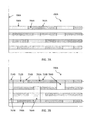
- FIGS. 6A-D illustrate the graphical representation of some design rules in some embodiments. More specifically, FIG. 6A shows a simplified graphical representation of a same track spacing rule 600 A between two gap blocks 612 A and 614 A along the same track 610 A.
- the same track spacing rule 600 A requires the spacing 608 A between the opposing ends of the two gap blocks 612 A (with neighboring shape 602 A) and 614 A (with neighboring shape 604 A) be greater than or equal to a prescribed value in some embodiments.
- the prescribed value may be constant or variable, depending upon the type of the shapes, the signals that these two shapes carry, the context (e.g., the surrounding shape(s) on the same layer or different layers) within which the two shapes, etc.
- the same track spacing rule When the empty space defined by the length 608 A between the opposing ends of 612 A and 614 A and the width associated with the track 610 A is identified as a gap rectangle 606 A, the same track spacing rule then requires that the gap rectangle 606 A must have at least a minimum length value as specified in the same track spacing rule as the prescribed spacing value 608 A.
- the same track spacing rule prescribes a minimum spacing value between the opposing ends of the gap blocks 612 A and 614 A.
- a common parallel projection occurs when the projected geometric entities of two gap blocks along the same direction overlap with each other in some embodiments. For example, gap blocks 612 A and 614 A share a common projection because the projection of 612 A and that of 614 A along the horizontal direction overlap each other.
- gap block 612 A and its neighboring shape 602 A and gap block 614 A appear to have the same width
- the widths of 612 A and 614 A may nevertheless differ at least in the context of gap blocks. This may be because gap blocks are formed with gap rectangles, and gap blocks 612 A and 614 A may thus have different widths. In some embodiments, gap block 612 A or gap block 614 A may span across multiple tracks.
- the widths of wires or interconnects 602 A and 604 A are identical because wires or interconnects not having the same width as the width value associated with the track 610 A may not be implemented along track 610 A. In either case (gap blocks having the same width or gap blocks having different width spanning across multiple tracks), gap blocks 612 A and 614 A share a common projection in, for example, the horizontal direction.
- FIG. 6B shows a simplified graphical representation of a one-track spacing rule 600 B in some embodiments.
- the one-track spacing rule applies when two gap blocks do not have a common parallel projection in either routing direction and are not separated by any tracks.
- the projection of gap block 612 B (with neighboring shape 602 B) and that of gap block 614 B (with neighboring shape 604 B) do not overlap each other regardless of which routing direction is selected for the projection.
- the one-track spacing 600 B requires that the spacing between two ends of the two gap blocks of interest be greater than or equal to a prescribed value.
- the spacing between gap block 612 B and gap block 614 B may be the horizontal spacing 606 B between two opposing ends of these two gap blocks. In some other embodiments, the spacing between these two gap blocks 612 B and 614 B may be the closest distance 616 B between these two gap blocks. In some embodiments, the two shapes include two gap blocks, and the two-track spacing requires a minimum spacing between the opposing ends of these two gap blocks 612 B and 614 B.
- FIG. 6C shows a simplified graphical representation of a two-track spacing rule 600 C in some embodiments.
- the two-track spacing rule applies when two shapes do not have a common parallel projection in either routing direction and are separated by one track. As illustrated in FIG. 6C , the projection of gap block 612 C (with neighboring shape 602 C) and that of gap block 614 C (with neighboring shape 604 C) do not overlap each other regardless of which routing direction is selected for the projection. In addition, there exist one track 608 C situated between shape 602 C and shape 604 C.
- the two-track spacing 600 C requires that the spacing between two ends of the two gap rectangles 612 C and 614 C be greater than or equal to a prescribed value.
- the spacing between gap block 612 C and gap block 614 C may include the horizontal spacing 606 C between two opposing ends of these two gap blocks 612 C and gap block 614 C. In some other embodiments, the spacing between these two gap blocks 612 C and 614 C may include the closest distance 610 C between these two gap blocks. In some embodiments, the two shapes include two gap blocks, and the two-track spacing requires a minimum spacing between the opposing ends of these two gap blocks 612 C and 614 C.
- FIG. 6D shows a simplified graphical representation of a more general N-track spacing rule 600 D in some embodiments where N includes a positive integer greater than two.
- the N-track spacing rule applies when two gap blocks do not have a common parallel projection in either routing direction and are separated by (N ⁇ 1) tracks.
- the projection of gap block 612 D (with neighboring shape 602 D) and that of gap block 614 D (with neighboring shape 604 D) do not overlap each other regardless of which routing direction is selected for the projection.
- the two track spacing 600 D requires that the spacing between two ends of the two gap blocks of interest be greater than or equal to a prescribed value.
- the spacing between gap block 612 D and gap block 614 D may include the horizontal spacing 606 D between two opposing ends of these two gap blocks.
- the spacing between these two gap blocks 612 D and 614 D may include the closest distance 616 D between these two gap blocks.
- the two shapes include two gap blocks, and the two-track spacing requires a minimum spacing between the opposing ends of these two gap blocks 612 D and 614 D.
- FIGS. 7A-H illustrate some simplified working examples to which some of the techniques described herein apply in some embodiments. More specifically, FIG. 7A illustrates a simplified portion of a layout 700 A including a plurality of tracks 706 A in the first direction. The portion also includes multiple shapes 702 A that represent electronic design components such as wires or interconnects in the portion of the layout.
- the geometric entities 704 A represent gap rectangles formed between two immediately neighboring shapes 702 A or between a shape 702 A and the boundary 708 A of the portion or the layout. As it can be seen from FIG. 7A , each gap rectangle is formed with the length along the first direction between the opposing ends of two shapes 702 A or between the boundary 708 A of the portion or the layout and the near end of a shape 702 A.
- Each gap rectangle is also formed with the width that is associated with its respective track 706 A. It shall be noted that in these embodiments illustrated in FIGS. 7A-H , the widths of the shapes 702 A also match those of their respective tracks because of, for example, a design rule that requires or desires that the width of a shape implemented along a track match the width associated with the track.
- FIG. 7B illustrates further progress of some methods or processes performed on the illustrated layout or the portion thereof. More specifically, FIG. 7B shows the creation of three gap blocks 702 B, 704 B, and 706 B from the respective groups of gap rectangles 704 A.
- gap block 702 B may be created by identifying or determining the common parallel projection of the respective four gap rectangles as the width of the gap block to be formed.
- the length of the gap block 702 B may be determined by spanning the gap block to cover area between the two outermost edges 708 B and 710 B of the gap rectangles of interest.
- FIG. 7B shows the creation of three gap blocks 702 B, 704 B, and 706 B from the respective groups of gap rectangles 704 A.
- gap block 702 B may be created by identifying or determining the common parallel projection of the respective four gap rectangles as the width of the gap block to be formed.
- the length of the gap block 702 B may be determined by spanning the gap block to cover area between the two outermost edges 708 B and 710 B
- FIG. 7B further illustrates splitting a larger gap rectangle 712 B (which is a part of the gap rectangles 704 A) into multiple smaller gap rectangles 714 B and 716 B if it is determined that the larger gap rectangle 712 B has certain size or dimension(s) such that the smaller gap rectangles 714 B and 716 B meet one or more design rules in some embodiments.
- the method or system may determine whether or not the spacing or closest distance between the smaller gap rectangles 714 B and 716 B satisfies the same track spacing requirement.
- FIGS. 7A-B also illustrate the legends used in FIGS. 7A-H .
- FIG. 7C illustrates further progress of some methods or processes performed on the illustrated layout or the portion thereof. More specifically, FIG. 7C illustrates the sibling link 702 C associated with the two gap rectangles labeled “1” and “6” in a portion of an electronic design 700 C. FIG. 7C further illustrates a lower gap link 706 C that associates gap block formed by the smaller gap rectangle labeled “1” and having a smaller coordinate along the first direction (e.g., the direction of the tracks) with the gap block labeled “3” having a larger coordinate along the first direction.
- FIG. 7C illustrates further progress of some methods or processes performed on the illustrated layout or the portion thereof. More specifically, FIG. 7C illustrates the sibling link 702 C associated with the two gap rectangles labeled “1” and “6” in a portion of an electronic design 700 C. FIG. 7C further illustrates a lower gap link 706 C that associates gap block formed by the smaller gap rectangle labeled “1” and having a smaller coordinate along the first direction (e
- FIG. 7C also illustrates a higher gap link 704 C that associates the smaller gap rectangle labeled “3” and having a larger coordinate along the first direction (e.g., the direction of the tracks) with the gap block formed from the smaller gap rectangle labeled “1” having a smaller coordinate along the first direction.
- a lower gap link is created from a shape having a larger coordinate to another shape having a smaller coordinate (and hence the term “lower”) in a particular direction (e.g., the direction of the track); and a higher gap link is created from a shape having a smaller coordinate to another shape having a larger coordinate (and hence the term “higher”) in the same direction.
- a higher gap link from a first gap block to a second gap block may be created when the second coordinate of a second reference point (e.g., the closest point to the first gap block) of the second gap block along a direction is larger than the first coordinate of a first reference point (e.g., a closest point to the second gap block) of the first gap block in the same direction.
- a second reference point e.g., the closest point to the first gap block
- various methods or systems may generate a higher gap link and/or a lower gap link between two non-overlapping shapes on separate tracks to indicate that the distance between or relative position of the two shapes fails to satisfy one or more design rules.
- the method or system generates both the lower gap link 706 C and the higher gap link 704 C to indicate that the spacing or closest distance between the gap block derived from the gap rectangle labeled “1” and the gap block labeled “3” violates one or more design rules.
- FIG. 7C illustrates an opposite link 708 C between the gap block labeled “4” and the gap block labeled “5” to indicate that these two gap blocks labeled “4” and “5” may have violated one or more pertinent design rules (e.g., the two-track spacing rule as described above in FIG. 6C ).
- FIG. 7D illustrates further progress of some methods or processes performed on the illustrated layout or the portion thereof. More specifically, FIG. 7D illustrates a real-time or after-the-fact design rule check indicating that the design 700 D as shown in FIG. 7C has violated one or more design rules between the gap block formed from the smaller gap rectangle labeled “1” and the gap block labeled “3”.
- the method or system generates both the lower gap link 706 D and the higher gap link 704 D (or inherits the higher gap link 704 C and lower gap link 706 C from FIG. 7C ) to indicate that the spacing or closest distance between the gap block derived from the gap rectangle labeled “1” and the gap block labeled “3” violates one or more design rules.
- the method or system may then adjust one or both gap blocks associated with the lower and higher gap links.
- the method or system adjusts the width of the gap block labeled “3” to a smaller width value in order to satisfy the one or more design rules violated by these two gap blocks as illustrated in FIG. 7C .
- the opposite link 708 C also indicates the violation of one or more design rules between the gap blocks labeled “4” and “5”.
- the method or system may adjust one or both shapes to fix the violation.
- the method or system adjusts the widths of both gap blocks labeled “4” and “5” to smaller width values.
- the method or system may then convert the opposite link into a higher gap link, a lower gap link, or both.
- the method or system converts the opposite link 708 C into the lower gap link 708 D and the higher gap link 710 D after the adjustment to both gap blocks.
- FIG. 7E illustrates that the method or system may split one or more gap blocks into multiple smaller sub-blocks along multiple tracks. More specifically, the gap block labeled “2” in the portion of electronic design 700 E illustrated in FIG. 7D is split into four sub-blocks 702 E; the adjusted gap block labeled “3” in FIG. 7D is split into three smaller sub-blocks 704 E; and the gap block labeled “4” in FIG. 7D is split into two smaller sub-blocks 706 E as illustrated in FIG. 7E .
- FIG. 7F illustrates the insertion of metal fills for the portion of the layout of FIG. 7E .
- the method or system may identify a sibling link between two sub-blocks and identify a first gap rectangle between these two sub-blocks that are associated with the sibling link. Once the gap rectangle is identified, the method or system may then insert metal fill in the empty space occupied by the first gap rectangle.
- the method or system identifies the sibling link 702 C enclosed by two sub-blocks in the portion of the electronic design 700 F, identifies the gap rectangle 702 F neighboring both sub-blocks, and inserts metal fill in the space occupied by the gap rectangle 702 F.
- FIG. 7G illustrates extensions of metal shapes for the portion of the layout of FIG. 7F .
- the method or system may identify a gap rectangle immediately adjacent to one or more sub-blocks that are not associated with any sibling links. Once the gap rectangle is identified, the method or system may then add metal extension to one or both ends of the second gap rectangle to fill the empty space between one or more existing metal shapes and the identified gap block. For example, the method may identify the gap rectangle 704 F (see FIG. 7F ) that is immediately adjacent to the gap block 708 G in the portion of the layout 700 G. The gap rectangle 704 F is not associated with any sibling links with other gap blocks or gap rectangles.
- the method or system may add metal extension 712 G to the space occupied by gap rectangle 704 F of FIG. 7F .
- This metal extension 712 G effectively extends the metal shape 714 G now occupying the space covered by both 714 G and 712 G illustrated in FIG. 7G .
- the method or system may similarly insert metal extension 710 G to extend metal shape 716 G.
- shapes 702 G represent metal extensions added by various methods or system described in this Application to extend existing metal shapes.
- FIG. 7H illustrates a finished portion of the layout. More specifically, FIG. 7H illustrates that the method or system may thus generate the finished portion of the layout by removing the gap blocks and the smaller sub-blocks from the portion 700 H illustrated in FIG. 7G . It shall be noted that although FIG. 7H still shows different patterns for the originally designed metal shapes 702 H as well as the metal extensions 704 H, the connected metal shape 702 H and metal extension 704 H are treated as one integral metal shape because they are designed to be manufactured as a single, integral metal shape. As described with reference to FIG. 7F, 706H indicates a metal fill element in the portion of the layout 700 H.
- FIG. 8 illustrates a block diagram of an illustrative computing system 800 suitable for enhancing manufacturability of electronic designs for multi-exposure lithography as described in the preceding paragraphs with reference to various figures.
- Computer system 800 includes a bus 806 or other communication mechanism for communicating information, which interconnects subsystems and devices, such as processor 807 , system memory 808 (e.g., RAM), static storage device 809 (e.g., ROM), disk drive 810 (e.g., magnetic or optical), communication interface 814 (e.g., modem or Ethernet card), display 811 (e.g., CRT or LCD), input device 812 (e.g., keyboard), and cursor control (not shown).
- processor 807 e.g., system memory 808 (e.g., RAM), static storage device 809 (e.g., ROM), disk drive 810 (e.g., magnetic or optical), communication interface 814 (e.g., modem or Ethernet card), display 811 (e.g.
- computer system 800 performs specific operations by one or more processor or processor cores 807 executing one or more sequences of one or more instructions contained in system memory 808 .
- Such instructions may be read into system memory 808 from another computer readable/usable storage medium, such as static storage device 809 or disk drive 810 .
- static storage device 809 or disk drive 810 may be used in place of or in combination with software instructions to implement the invention.
- hard-wired circuitry may be used in place of or in combination with software instructions to implement the invention.
- embodiments of the invention are not limited to any specific combination of hardware circuitry and/or software.
- the term “logic” shall mean any combination of software or hardware that is used to implement all or part of the invention.
- Various actions or processes as described in the preceding paragraphs may be performed by using one or more processors, one or more processor cores, or combination thereof 807 , where the one or more processors, one or more processor cores, or combination thereof executes one or more threads.
- the act of specifying various net or terminal sets or the act or module of performing verification or simulation, etc. may be performed by one or more processors, one or more processor cores, or combination thereof.
- the parasitic extraction, current solving, current density computation and current or current density verification is done in memory as layout objects or nets are created or modified.
- Non-volatile media includes, for example, optical or magnetic disks, such as disk drive 810 .
- Volatile media includes dynamic memory, such as system memory 808 .
- Computer readable storage media includes, for example, electromechanical disk drives (such as a floppy disk, a flexible disk, or a hard disk), a flash-based, RAM-based (such as SRAM, DRAM, SDRAM, DDR, MRAM, etc.), or any other solid-state drives (SSD), magnetic tape, any other magnetic or magneto-optical medium, CD-ROM, any other optical medium, any other physical medium with patterns of holes, RAM, PROM, EPROM, FLASH-EPROM, any other memory chip or cartridge, or any other medium from which a computer can read.
- electromechanical disk drives such as a floppy disk, a flexible disk, or a hard disk
- RAM-based such as SRAM, DRAM, SDRAM, DDR, MRAM, etc.
- SSD solid-state drives
- magnetic tape any other magnetic or magneto-optical medium
- CD-ROM any other optical medium
- any other physical medium with patterns of holes RAM, PROM, EPROM, FLASH-EPROM, any other memory chip or cartridge, or any other
- execution of the sequences of instructions to practice the invention is performed by a single computer system 800 .
- two or more computer systems 800 coupled by communication link 815 may perform the sequence of instructions required to practice the invention in coordination with one another.
- Computer system 800 may transmit and receive messages, data, and instructions, including program, i.e., application code, through communication link 815 and communication interface 814 .
- Received program code may be executed by processor 807 as it is received, and/or stored in disk drive 810 , or other non-volatile storage for later execution.
- the computer system 800 operates in conjunction with a data storage system 831 , e.g., a data storage system 831 that includes a database 832 that is readily accessible by the computer system 800 .
- the computer system 800 communicates with the data storage system 831 through a data interface 833 .
- a data interface 833 which is coupled to the bus 806 (e.g., memory bus, system bus, data bus, etc.), transmits and receives electrical, electromagnetic or optical signals that include data streams representing various types of signal information, e.g., instructions, messages and data.
- the functions of the data interface 833 may be performed by the communication interface 814 .
Landscapes
- Physics & Mathematics (AREA)
- General Physics & Mathematics (AREA)
- Design And Manufacture Of Integrated Circuits (AREA)
Abstract
Description
Claims (28)
Priority Applications (1)
| Application Number | Priority Date | Filing Date | Title |
|---|---|---|---|
| US14/320,594 US9767245B1 (en) | 2014-06-30 | 2014-06-30 | Method, system, and computer program product for improving mask designs and manufacturability of electronic designs for multi-exposure lithography |
Applications Claiming Priority (1)
| Application Number | Priority Date | Filing Date | Title |
|---|---|---|---|
| US14/320,594 US9767245B1 (en) | 2014-06-30 | 2014-06-30 | Method, system, and computer program product for improving mask designs and manufacturability of electronic designs for multi-exposure lithography |
Publications (1)
| Publication Number | Publication Date |
|---|---|
| US9767245B1 true US9767245B1 (en) | 2017-09-19 |
Family
ID=59828524
Family Applications (1)
| Application Number | Title | Priority Date | Filing Date |
|---|---|---|---|
| US14/320,594 Active 2034-08-16 US9767245B1 (en) | 2014-06-30 | 2014-06-30 | Method, system, and computer program product for improving mask designs and manufacturability of electronic designs for multi-exposure lithography |
Country Status (1)
| Country | Link |
|---|---|
| US (1) | US9767245B1 (en) |
Citations (33)
| Publication number | Priority date | Publication date | Assignee | Title |
|---|---|---|---|---|
| US5861342A (en) * | 1995-12-26 | 1999-01-19 | Vlsi Technology, Inc. | Optimized structures for dummy fill mask design |
| US6543041B1 (en) | 1999-06-15 | 2003-04-01 | Cadence Design Systems, Inc. | Method and apparatus for reducing signal integrity and reliability problems in ICS through netlist changes during placement |
| US20030229479A1 (en) * | 2002-06-07 | 2003-12-11 | Smith Taber H. | Dummy fill for integrated circuits |
| US20030228714A1 (en) * | 2002-06-07 | 2003-12-11 | Smith Taber H. | Dummy fill for integrated circuits |
| US20040044978A1 (en) * | 2002-08-28 | 2004-03-04 | Werner Juengling | Pattern generation on a semiconductor surface |
| US20050064634A1 (en) * | 2003-09-24 | 2005-03-24 | Infineon Technologies North America Corp. | Structure and method for placement, sizing and shaping of dummy structures |
| US6981235B1 (en) | 2003-01-14 | 2005-12-27 | Cadence Design Systems, Inc. | Nearest neighbor mechanism |
| US7089526B1 (en) | 2003-01-14 | 2006-08-08 | Cadence Design Systems, Inc. | Maximum flow analysis for electronic circuit design |
| US7100129B1 (en) | 2003-01-14 | 2006-08-29 | Cadence Design Systems, Inc. | Hierarchical gcell method and mechanism |
| US7100128B1 (en) | 2003-01-14 | 2006-08-29 | Cadence Design Systems, Inc. | Zone tree method and mechanism |
| US20080066027A1 (en) | 2006-09-13 | 2008-03-13 | Stefanus Mantik | Computationally efficient design rule checking for circuit interconnect routing design |
| US20090055793A1 (en) * | 2007-08-22 | 2009-02-26 | Hanno Melzner | Method of making an integrated circuit having fill structures |
| US20090319969A1 (en) | 2008-06-20 | 2009-12-24 | Lizheng Zhang | Method and system for performing statistical leakage characterization, analysis, and modeling |
| US7676781B1 (en) | 2003-01-14 | 2010-03-09 | Cadence Design Systems, Inc. | Method and mechanism for implementing a minimum spanning tree |
| US20100083198A1 (en) | 2008-09-30 | 2010-04-01 | Lizheng Zhang | Method and system for performing statistical leakage characterization, analysis, and modeling |
| US20110014786A1 (en) * | 2009-07-16 | 2011-01-20 | Cadence Design Systems, Inc. | Method, system, and program product for routing an integrated circuit to be manufactured by doubled patterning |
| US8065652B1 (en) | 2007-08-13 | 2011-11-22 | Cadence Design Systems, Inc. | Method and system for determining hard and preferred rules in global routing of electronic designs |
| US8151229B1 (en) | 2007-04-10 | 2012-04-03 | Cadence Design Systems, Inc. | System and method of computing pin criticalities under process variations for timing analysis and optimization |
| US20120190188A1 (en) * | 2010-12-15 | 2012-07-26 | Chao Zhao | Method for filling a gap |
| US8336010B1 (en) | 2009-12-04 | 2012-12-18 | Cadence Design Systems, Inc. | Design-specific on chip variation de-rating factors for static timing analysis of integrated circuits |
| US8375348B1 (en) | 2010-12-29 | 2013-02-12 | Cadence Design Systems, Inc. | Method, system, and program product to implement colored tiles for detail routing for double pattern lithography |
| US8560998B1 (en) | 2010-12-29 | 2013-10-15 | Cadence Design Systems, Inc. | Method, system, and program product to implement C-routing for double pattern lithography |
| US8640080B1 (en) | 2012-06-01 | 2014-01-28 | Cadence Design Systems, Inc. | Method and system for visualizing pin access locations |
| US8671368B1 (en) | 2010-12-29 | 2014-03-11 | Cadence Design Systems, Inc. | Method, system, and program product to implement detail routing for double pattern lithography |
| US8782570B1 (en) | 2012-05-07 | 2014-07-15 | Cadence Design Systems, Inc. | Methods, systems, and articles of manufacture for implementing a physical electronic circuit design with multiple-patterning techniques |
| US8863048B1 (en) | 2013-03-15 | 2014-10-14 | Cadence Design Systems, Inc. | Methods, systems, and articles of manufacture for implementing multiple-patterning-aware correct-by-construction layout processing for an electronic design |
| US20140359548A1 (en) | 2013-06-03 | 2014-12-04 | International Business Machines Corporation | Orthogonal circuit element routing |
| US8935649B1 (en) | 2012-08-31 | 2015-01-13 | Cadence Design Systems, Inc. | Methods, systems, and articles of manufacture for routing an electronic design using spacetiles |
| US8984465B1 (en) | 2013-06-28 | 2015-03-17 | Cadence Design Systems, Inc. | Methods, systems, and articles of manufacture for automatically assigning track patterns to regions for physical implementation of an electronic design |
| US9003349B1 (en) | 2013-06-28 | 2015-04-07 | Cadence Design Systems, Inc. | Methods, systems, and articles of manufacture for implementing a physical electronic design with area-bounded tracks |
| US9087174B1 (en) | 2013-03-15 | 2015-07-21 | Cadence Design Systems, Inc. | Methods, systems, and articles of manufacture for implementing multiple-patterning-aware design rule check for electronic designs |
| US9104830B1 (en) | 2013-06-28 | 2015-08-11 | Cadence Design Systems, Inc. | Methods, systems, and articles of manufacture for assigning track patterns to regions of an electronic design |
| US9117052B1 (en) | 2012-04-12 | 2015-08-25 | Cadence Design Systems, Inc. | Methods, systems, and articles of manufacture for interactively implementing physical electronic designs with track patterns |
-
2014
- 2014-06-30 US US14/320,594 patent/US9767245B1/en active Active
Patent Citations (39)
| Publication number | Priority date | Publication date | Assignee | Title |
|---|---|---|---|---|
| US5861342A (en) * | 1995-12-26 | 1999-01-19 | Vlsi Technology, Inc. | Optimized structures for dummy fill mask design |
| US6543041B1 (en) | 1999-06-15 | 2003-04-01 | Cadence Design Systems, Inc. | Method and apparatus for reducing signal integrity and reliability problems in ICS through netlist changes during placement |
| US20030229479A1 (en) * | 2002-06-07 | 2003-12-11 | Smith Taber H. | Dummy fill for integrated circuits |
| US20030228714A1 (en) * | 2002-06-07 | 2003-12-11 | Smith Taber H. | Dummy fill for integrated circuits |
| US20040044978A1 (en) * | 2002-08-28 | 2004-03-04 | Werner Juengling | Pattern generation on a semiconductor surface |
| US7100129B1 (en) | 2003-01-14 | 2006-08-29 | Cadence Design Systems, Inc. | Hierarchical gcell method and mechanism |
| US7594214B1 (en) | 2003-01-14 | 2009-09-22 | Cadence Design Systems, Inc. | Maximum flow analysis for electronic circuit design |
| US7089526B1 (en) | 2003-01-14 | 2006-08-08 | Cadence Design Systems, Inc. | Maximum flow analysis for electronic circuit design |
| US8117569B1 (en) | 2003-01-14 | 2012-02-14 | Cadence Design Systems, Inc. | Method and mechanism for implementing a minimum spanning tree |
| US7100128B1 (en) | 2003-01-14 | 2006-08-29 | Cadence Design Systems, Inc. | Zone tree method and mechanism |
| US7676781B1 (en) | 2003-01-14 | 2010-03-09 | Cadence Design Systems, Inc. | Method and mechanism for implementing a minimum spanning tree |
| US6981235B1 (en) | 2003-01-14 | 2005-12-27 | Cadence Design Systems, Inc. | Nearest neighbor mechanism |
| US20050064634A1 (en) * | 2003-09-24 | 2005-03-24 | Infineon Technologies North America Corp. | Structure and method for placement, sizing and shaping of dummy structures |
| US20080066027A1 (en) | 2006-09-13 | 2008-03-13 | Stefanus Mantik | Computationally efficient design rule checking for circuit interconnect routing design |
| US8151229B1 (en) | 2007-04-10 | 2012-04-03 | Cadence Design Systems, Inc. | System and method of computing pin criticalities under process variations for timing analysis and optimization |
| US8065652B1 (en) | 2007-08-13 | 2011-11-22 | Cadence Design Systems, Inc. | Method and system for determining hard and preferred rules in global routing of electronic designs |
| US20090055793A1 (en) * | 2007-08-22 | 2009-02-26 | Hanno Melzner | Method of making an integrated circuit having fill structures |
| US20090319969A1 (en) | 2008-06-20 | 2009-12-24 | Lizheng Zhang | Method and system for performing statistical leakage characterization, analysis, and modeling |
| US8086978B2 (en) | 2008-06-20 | 2011-12-27 | Cadence Design Systems, Inc. | Method and system for performing statistical leakage characterization, analysis, and modeling |
| US8069432B2 (en) | 2008-09-30 | 2011-11-29 | Cadence Design Systems, Inc. | Method and system for performing statistical leakage characterization, analysis, and modeling |
| US20100083198A1 (en) | 2008-09-30 | 2010-04-01 | Lizheng Zhang | Method and system for performing statistical leakage characterization, analysis, and modeling |
| US20110014786A1 (en) * | 2009-07-16 | 2011-01-20 | Cadence Design Systems, Inc. | Method, system, and program product for routing an integrated circuit to be manufactured by doubled patterning |
| US8782586B2 (en) | 2009-07-16 | 2014-07-15 | Cadence Design Systems, Inc. | Method, system, and program product for routing an integrated circuit to be manufactured by doubled patterning |
| US8762908B1 (en) | 2009-12-04 | 2014-06-24 | Cadence Design Systems, Inc. | Static timing analysis with design-specific on chip variation de-rating factors |
| US8336010B1 (en) | 2009-12-04 | 2012-12-18 | Cadence Design Systems, Inc. | Design-specific on chip variation de-rating factors for static timing analysis of integrated circuits |
| US20120190188A1 (en) * | 2010-12-15 | 2012-07-26 | Chao Zhao | Method for filling a gap |
| US8375348B1 (en) | 2010-12-29 | 2013-02-12 | Cadence Design Systems, Inc. | Method, system, and program product to implement colored tiles for detail routing for double pattern lithography |
| US8671368B1 (en) | 2010-12-29 | 2014-03-11 | Cadence Design Systems, Inc. | Method, system, and program product to implement detail routing for double pattern lithography |
| US8560998B1 (en) | 2010-12-29 | 2013-10-15 | Cadence Design Systems, Inc. | Method, system, and program product to implement C-routing for double pattern lithography |
| US9117052B1 (en) | 2012-04-12 | 2015-08-25 | Cadence Design Systems, Inc. | Methods, systems, and articles of manufacture for interactively implementing physical electronic designs with track patterns |
| US8782570B1 (en) | 2012-05-07 | 2014-07-15 | Cadence Design Systems, Inc. | Methods, systems, and articles of manufacture for implementing a physical electronic circuit design with multiple-patterning techniques |
| US8640080B1 (en) | 2012-06-01 | 2014-01-28 | Cadence Design Systems, Inc. | Method and system for visualizing pin access locations |
| US8935649B1 (en) | 2012-08-31 | 2015-01-13 | Cadence Design Systems, Inc. | Methods, systems, and articles of manufacture for routing an electronic design using spacetiles |
| US8863048B1 (en) | 2013-03-15 | 2014-10-14 | Cadence Design Systems, Inc. | Methods, systems, and articles of manufacture for implementing multiple-patterning-aware correct-by-construction layout processing for an electronic design |
| US9087174B1 (en) | 2013-03-15 | 2015-07-21 | Cadence Design Systems, Inc. | Methods, systems, and articles of manufacture for implementing multiple-patterning-aware design rule check for electronic designs |
| US20140359548A1 (en) | 2013-06-03 | 2014-12-04 | International Business Machines Corporation | Orthogonal circuit element routing |
| US8984465B1 (en) | 2013-06-28 | 2015-03-17 | Cadence Design Systems, Inc. | Methods, systems, and articles of manufacture for automatically assigning track patterns to regions for physical implementation of an electronic design |
| US9003349B1 (en) | 2013-06-28 | 2015-04-07 | Cadence Design Systems, Inc. | Methods, systems, and articles of manufacture for implementing a physical electronic design with area-bounded tracks |
| US9104830B1 (en) | 2013-06-28 | 2015-08-11 | Cadence Design Systems, Inc. | Methods, systems, and articles of manufacture for assigning track patterns to regions of an electronic design |
Similar Documents
| Publication | Publication Date | Title |
|---|---|---|
| US8782570B1 (en) | Methods, systems, and articles of manufacture for implementing a physical electronic circuit design with multiple-patterning techniques | |
| US9396301B1 (en) | Method, system, and computer program product for interconnecting circuit components with track patterns for electronic circuit designs | |
| US11222157B2 (en) | Pin access hybrid cell height design | |
| US9659138B1 (en) | Methods, systems, and computer program product for a bottom-up electronic design implementation flow and track pattern definition for multiple-patterning lithographic techniques | |
| US9904756B1 (en) | Methods, systems, and computer program product for implementing DRC clean multi-patterning process nodes with lateral fills in electronic designs | |
| US9652579B1 (en) | Methods, systems, and computer program product for implementing DRC clean multi-patterning process nodes with parallel fills in electronic designs | |
| US8516402B1 (en) | Method and apparatus for automatically fixing double patterning loop violations | |
| US8473874B1 (en) | Method and apparatus for automatically fixing double patterning loop violations | |
| US9613175B2 (en) | Method, computer system and computer-readable storage medium for creating a layout of an integrated circuit | |
| US8527930B2 (en) | Generating and using route fix guidance | |
| US8683392B2 (en) | Double patterning methodology | |
| JP4474404B2 (en) | Packing-based macro placement method and semiconductor chip using the same | |
| US9003349B1 (en) | Methods, systems, and articles of manufacture for implementing a physical electronic design with area-bounded tracks | |
| US9372955B1 (en) | Method, system, and computer program product for implementing repetitive track patterns for electronic circuit designs | |
| US8984465B1 (en) | Methods, systems, and articles of manufacture for automatically assigning track patterns to regions for physical implementation of an electronic design | |
| US20230385514A1 (en) | Using machine trained network during routing to modify locations of vias in an ic design | |
| US9087174B1 (en) | Methods, systems, and articles of manufacture for implementing multiple-patterning-aware design rule check for electronic designs | |
| US20230306177A1 (en) | Using topological and geometric routers to produce curvilinear routes | |
| US9372952B1 (en) | Methods, systems, and articles of manufacture for enhancing metrics of electronic designs using design rule driven physical design implementation techniques | |
| US10192018B1 (en) | Method and system for implementing efficient trim data representation for an electronic design | |
| US9563737B1 (en) | Method, system, and computer program product for checking or verifying shapes in track patterns for electronic circuit designs | |
| US9286432B1 (en) | Methods, systems, and articles of manufacture for implementing correct-by-construction physical designs with multiple-patterning-awareness | |
| US9183343B1 (en) | Methods, systems, and articles of manufacture for implementing high current carrying interconnects in electronic designs | |
| US8935649B1 (en) | Methods, systems, and articles of manufacture for routing an electronic design using spacetiles | |
| US8914763B1 (en) | Methods, systems, and articles of manufacture for generating multi-layer local maximal orthogonal routing paths in fractured space |
Legal Events
| Date | Code | Title | Description |
|---|---|---|---|
| AS | Assignment |
Owner name: CADENCE DESIGN SYSTEMS, INC., CALIFORNIA Free format text: ASSIGNMENT OF ASSIGNORS INTEREST;ASSIGNORS:MANTIK, STEFANUS;GEROUSIS, VASSILIOS C.;REEL/FRAME:033216/0448 Effective date: 20140626 |
|
| FEPP | Fee payment procedure |
Free format text: PAYOR NUMBER ASSIGNED (ORIGINAL EVENT CODE: ASPN) |
|
| STCF | Information on status: patent grant |
Free format text: PATENTED CASE |
|
| MAFP | Maintenance fee payment |
Free format text: PAYMENT OF MAINTENANCE FEE, 4TH YEAR, LARGE ENTITY (ORIGINAL EVENT CODE: M1551); ENTITY STATUS OF PATENT OWNER: LARGE ENTITY Year of fee payment: 4 |
|
| MAFP | Maintenance fee payment |
Free format text: PAYMENT OF MAINTENANCE FEE, 8TH YEAR, LARGE ENTITY (ORIGINAL EVENT CODE: M1552); ENTITY STATUS OF PATENT OWNER: LARGE ENTITY Year of fee payment: 8 |