US9711402B1 - Method of forming contact metal - Google Patents
Method of forming contact metal Download PDFInfo
- Publication number
- US9711402B1 US9711402B1 US15/063,905 US201615063905A US9711402B1 US 9711402 B1 US9711402 B1 US 9711402B1 US 201615063905 A US201615063905 A US 201615063905A US 9711402 B1 US9711402 B1 US 9711402B1
- Authority
- US
- United States
- Prior art keywords
- layer
- forming
- over
- tin
- source
- Prior art date
- Legal status (The legal status is an assumption and is not a legal conclusion. Google has not performed a legal analysis and makes no representation as to the accuracy of the status listed.)
- Active
Links
Images


Classifications
-
- H10W20/0698—
-
- H—ELECTRICITY
- H01—ELECTRIC ELEMENTS
- H01L—SEMICONDUCTOR DEVICES NOT COVERED BY CLASS H10
- H01L21/00—Processes or apparatus adapted for the manufacture or treatment of semiconductor or solid state devices or of parts thereof
- H01L21/70—Manufacture or treatment of devices consisting of a plurality of solid state components formed in or on a common substrate or of parts thereof; Manufacture of integrated circuit devices or of parts thereof
- H01L21/71—Manufacture of specific parts of devices defined in group H01L21/70
- H01L21/768—Applying interconnections to be used for carrying current between separate components within a device comprising conductors and dielectrics
- H01L21/76838—Applying interconnections to be used for carrying current between separate components within a device comprising conductors and dielectrics characterised by the formation and the after-treatment of the conductors
- H01L21/76895—Local interconnects; Local pads, as exemplified by patent document EP0896365
-
- H—ELECTRICITY
- H10—SEMICONDUCTOR DEVICES; ELECTRIC SOLID-STATE DEVICES NOT OTHERWISE PROVIDED FOR
- H10D—INORGANIC ELECTRIC SEMICONDUCTOR DEVICES
- H10D84/00—Integrated devices formed in or on semiconductor substrates that comprise only semiconducting layers, e.g. on Si wafers or on GaAs-on-Si wafers
- H10D84/01—Manufacture or treatment
- H10D84/0123—Integrating together multiple components covered by H10D12/00 or H10D30/00, e.g. integrating multiple IGBTs
- H10D84/0126—Integrating together multiple components covered by H10D12/00 or H10D30/00, e.g. integrating multiple IGBTs the components including insulated gates, e.g. IGFETs
- H10D84/0158—Integrating together multiple components covered by H10D12/00 or H10D30/00, e.g. integrating multiple IGBTs the components including insulated gates, e.g. IGFETs the components including FinFETs
-
- H—ELECTRICITY
- H01—ELECTRIC ELEMENTS
- H01L—SEMICONDUCTOR DEVICES NOT COVERED BY CLASS H10
- H01L21/00—Processes or apparatus adapted for the manufacture or treatment of semiconductor or solid state devices or of parts thereof
- H01L21/70—Manufacture or treatment of devices consisting of a plurality of solid state components formed in or on a common substrate or of parts thereof; Manufacture of integrated circuit devices or of parts thereof
- H01L21/71—Manufacture of specific parts of devices defined in group H01L21/70
- H01L21/768—Applying interconnections to be used for carrying current between separate components within a device comprising conductors and dielectrics
- H01L21/76801—Applying interconnections to be used for carrying current between separate components within a device comprising conductors and dielectrics characterised by the formation and the after-treatment of the dielectrics, e.g. smoothing
- H01L21/76802—Applying interconnections to be used for carrying current between separate components within a device comprising conductors and dielectrics characterised by the formation and the after-treatment of the dielectrics, e.g. smoothing by forming openings in dielectrics
- H01L21/76805—Applying interconnections to be used for carrying current between separate components within a device comprising conductors and dielectrics characterised by the formation and the after-treatment of the dielectrics, e.g. smoothing by forming openings in dielectrics the opening being a via or contact hole penetrating the underlying conductor
-
- H—ELECTRICITY
- H01—ELECTRIC ELEMENTS
- H01L—SEMICONDUCTOR DEVICES NOT COVERED BY CLASS H10
- H01L21/00—Processes or apparatus adapted for the manufacture or treatment of semiconductor or solid state devices or of parts thereof
- H01L21/70—Manufacture or treatment of devices consisting of a plurality of solid state components formed in or on a common substrate or of parts thereof; Manufacture of integrated circuit devices or of parts thereof
- H01L21/71—Manufacture of specific parts of devices defined in group H01L21/70
- H01L21/768—Applying interconnections to be used for carrying current between separate components within a device comprising conductors and dielectrics
- H01L21/76838—Applying interconnections to be used for carrying current between separate components within a device comprising conductors and dielectrics characterised by the formation and the after-treatment of the conductors
- H01L21/76841—Barrier, adhesion or liner layers
- H01L21/76843—Barrier, adhesion or liner layers formed in openings in a dielectric
-
- H—ELECTRICITY
- H01—ELECTRIC ELEMENTS
- H01L—SEMICONDUCTOR DEVICES NOT COVERED BY CLASS H10
- H01L21/00—Processes or apparatus adapted for the manufacture or treatment of semiconductor or solid state devices or of parts thereof
- H01L21/70—Manufacture or treatment of devices consisting of a plurality of solid state components formed in or on a common substrate or of parts thereof; Manufacture of integrated circuit devices or of parts thereof
- H01L21/71—Manufacture of specific parts of devices defined in group H01L21/70
- H01L21/768—Applying interconnections to be used for carrying current between separate components within a device comprising conductors and dielectrics
- H01L21/76838—Applying interconnections to be used for carrying current between separate components within a device comprising conductors and dielectrics characterised by the formation and the after-treatment of the conductors
- H01L21/76886—Modifying permanently or temporarily the pattern or the conductivity of conductive members, e.g. formation of alloys, reduction of contact resistances
- H01L21/76889—Modifying permanently or temporarily the pattern or the conductivity of conductive members, e.g. formation of alloys, reduction of contact resistances by forming silicides of refractory metals
-
- H01L21/823814—
-
- H01L21/823821—
-
- H01L21/823871—
-
- H—ELECTRICITY
- H10—SEMICONDUCTOR DEVICES; ELECTRIC SOLID-STATE DEVICES NOT OTHERWISE PROVIDED FOR
- H10D—INORGANIC ELECTRIC SEMICONDUCTOR DEVICES
- H10D30/00—Field-effect transistors [FET]
- H10D30/01—Manufacture or treatment
- H10D30/021—Manufacture or treatment of FETs having insulated gates [IGFET]
- H10D30/0212—Manufacture or treatment of FETs having insulated gates [IGFET] using self-aligned silicidation
-
- H—ELECTRICITY
- H10—SEMICONDUCTOR DEVICES; ELECTRIC SOLID-STATE DEVICES NOT OTHERWISE PROVIDED FOR
- H10D—INORGANIC ELECTRIC SEMICONDUCTOR DEVICES
- H10D30/00—Field-effect transistors [FET]
- H10D30/01—Manufacture or treatment
- H10D30/021—Manufacture or treatment of FETs having insulated gates [IGFET]
- H10D30/024—Manufacture or treatment of FETs having insulated gates [IGFET] of fin field-effect transistors [FinFET]
-
- H—ELECTRICITY
- H10—SEMICONDUCTOR DEVICES; ELECTRIC SOLID-STATE DEVICES NOT OTHERWISE PROVIDED FOR
- H10D—INORGANIC ELECTRIC SEMICONDUCTOR DEVICES
- H10D30/00—Field-effect transistors [FET]
- H10D30/60—Insulated-gate field-effect transistors [IGFET]
- H10D30/62—Fin field-effect transistors [FinFET]
- H10D30/6211—Fin field-effect transistors [FinFET] having fin-shaped semiconductor bodies integral with the bulk semiconductor substrates
-
- H—ELECTRICITY
- H10—SEMICONDUCTOR DEVICES; ELECTRIC SOLID-STATE DEVICES NOT OTHERWISE PROVIDED FOR
- H10D—INORGANIC ELECTRIC SEMICONDUCTOR DEVICES
- H10D30/00—Field-effect transistors [FET]
- H10D30/60—Insulated-gate field-effect transistors [IGFET]
- H10D30/62—Fin field-effect transistors [FinFET]
- H10D30/6219—Fin field-effect transistors [FinFET] characterised by the source or drain electrodes
-
- H—ELECTRICITY
- H10—SEMICONDUCTOR DEVICES; ELECTRIC SOLID-STATE DEVICES NOT OTHERWISE PROVIDED FOR
- H10D—INORGANIC ELECTRIC SEMICONDUCTOR DEVICES
- H10D84/00—Integrated devices formed in or on semiconductor substrates that comprise only semiconducting layers, e.g. on Si wafers or on GaAs-on-Si wafers
- H10D84/01—Manufacture or treatment
- H10D84/0123—Integrating together multiple components covered by H10D12/00 or H10D30/00, e.g. integrating multiple IGBTs
- H10D84/0126—Integrating together multiple components covered by H10D12/00 or H10D30/00, e.g. integrating multiple IGBTs the components including insulated gates, e.g. IGFETs
- H10D84/0149—Manufacturing their interconnections or electrodes, e.g. source or drain electrodes
-
- H—ELECTRICITY
- H10—SEMICONDUCTOR DEVICES; ELECTRIC SOLID-STATE DEVICES NOT OTHERWISE PROVIDED FOR
- H10D—INORGANIC ELECTRIC SEMICONDUCTOR DEVICES
- H10D84/00—Integrated devices formed in or on semiconductor substrates that comprise only semiconducting layers, e.g. on Si wafers or on GaAs-on-Si wafers
- H10D84/01—Manufacture or treatment
- H10D84/0123—Integrating together multiple components covered by H10D12/00 or H10D30/00, e.g. integrating multiple IGBTs
- H10D84/0126—Integrating together multiple components covered by H10D12/00 or H10D30/00, e.g. integrating multiple IGBTs the components including insulated gates, e.g. IGFETs
- H10D84/0165—Integrating together multiple components covered by H10D12/00 or H10D30/00, e.g. integrating multiple IGBTs the components including insulated gates, e.g. IGFETs the components including complementary IGFETs, e.g. CMOS devices
- H10D84/017—Manufacturing their source or drain regions, e.g. silicided source or drain regions
-
- H—ELECTRICITY
- H10—SEMICONDUCTOR DEVICES; ELECTRIC SOLID-STATE DEVICES NOT OTHERWISE PROVIDED FOR
- H10D—INORGANIC ELECTRIC SEMICONDUCTOR DEVICES
- H10D84/00—Integrated devices formed in or on semiconductor substrates that comprise only semiconducting layers, e.g. on Si wafers or on GaAs-on-Si wafers
- H10D84/01—Manufacture or treatment
- H10D84/0123—Integrating together multiple components covered by H10D12/00 or H10D30/00, e.g. integrating multiple IGBTs
- H10D84/0126—Integrating together multiple components covered by H10D12/00 or H10D30/00, e.g. integrating multiple IGBTs the components including insulated gates, e.g. IGFETs
- H10D84/0165—Integrating together multiple components covered by H10D12/00 or H10D30/00, e.g. integrating multiple IGBTs the components including insulated gates, e.g. IGFETs the components including complementary IGFETs, e.g. CMOS devices
- H10D84/0186—Manufacturing their interconnections or electrodes, e.g. source or drain electrodes
-
- H—ELECTRICITY
- H10—SEMICONDUCTOR DEVICES; ELECTRIC SOLID-STATE DEVICES NOT OTHERWISE PROVIDED FOR
- H10D—INORGANIC ELECTRIC SEMICONDUCTOR DEVICES
- H10D84/00—Integrated devices formed in or on semiconductor substrates that comprise only semiconducting layers, e.g. on Si wafers or on GaAs-on-Si wafers
- H10D84/01—Manufacture or treatment
- H10D84/0123—Integrating together multiple components covered by H10D12/00 or H10D30/00, e.g. integrating multiple IGBTs
- H10D84/0126—Integrating together multiple components covered by H10D12/00 or H10D30/00, e.g. integrating multiple IGBTs the components including insulated gates, e.g. IGFETs
- H10D84/0165—Integrating together multiple components covered by H10D12/00 or H10D30/00, e.g. integrating multiple IGBTs the components including insulated gates, e.g. IGFETs the components including complementary IGFETs, e.g. CMOS devices
- H10D84/0193—Integrating together multiple components covered by H10D12/00 or H10D30/00, e.g. integrating multiple IGBTs the components including insulated gates, e.g. IGFETs the components including complementary IGFETs, e.g. CMOS devices the components including FinFETs
-
- H—ELECTRICITY
- H10—SEMICONDUCTOR DEVICES; ELECTRIC SOLID-STATE DEVICES NOT OTHERWISE PROVIDED FOR
- H10D—INORGANIC ELECTRIC SEMICONDUCTOR DEVICES
- H10D84/00—Integrated devices formed in or on semiconductor substrates that comprise only semiconducting layers, e.g. on Si wafers or on GaAs-on-Si wafers
- H10D84/01—Manufacture or treatment
- H10D84/02—Manufacture or treatment characterised by using material-based technologies
- H10D84/03—Manufacture or treatment characterised by using material-based technologies using Group IV technology, e.g. silicon technology or silicon-carbide [SiC] technology
- H10D84/038—Manufacture or treatment characterised by using material-based technologies using Group IV technology, e.g. silicon technology or silicon-carbide [SiC] technology using silicon technology, e.g. SiGe
-
- H10W20/033—
-
- H10W20/056—
-
- H10W20/066—
-
- H10W20/083—
-
- H10W20/084—
Definitions
- This scaling down process generally provides benefits by increasing production efficiency and lowering associated costs. Such scaling down has also increased the complexity of IC processing and manufacturing. For these advances to be realized, similar developments in IC processing and manufacturing are needed.
- One area is the wiring, or interconnects, between the transistors and other devices.
- existing methods of fabricating IC devices have been generally adequate for their intended purposes, they have not been entirely satisfactory in all respects. For example, improvements in the process of forming of a contact metal in a FinFET device are desired.
- FIG. 1 is a flowchart of an example method for fabricating a semiconductor device constructed in accordance with some embodiments.
- FIG. 2A is a diagrammatic perspective view of an initial structure of an example semiconductor device in accordance with some embodiments.
- FIG. 2B is a cross section view of an example of the initial structure in accordance with some embodiments, along the line A-A in FIG. 2A .
- FIGS. 3A, 3B, 4A, 4B, 5A, 5B, 6A, 6B, 7A, 7B, 8A and 8B are cross-sectional views of an example semiconductor device in accordance with some embodiments, along the line A-A in FIG. 2A .
- first and second features are formed in direct contact
- additional features may be formed between the first and second features, such that the first and second features may not be in direct contact
- present disclosure may repeat reference numerals and/or letters in the various examples. This repetition is for the purpose of simplicity and clarity and does not in itself dictate a relationship between the various embodiments and/or configurations discussed.
- spatially relative terms such as “beneath,” “below,” “lower,” “above,” “upper” and the like, may be used herein for ease of description to describe one element or feature's relationship to another element(s) or feature(s) as illustrated in the figures.
- the spatially relative terms are intended to encompass different orientations of the device in use or operation in addition to the orientation depicted in the figures.
- the apparatus may be otherwise oriented (rotated 90 degrees or at other orientations) and the spatially relative descriptors used herein may likewise be interpreted accordingly.
- the present disclosure is directed to, but not otherwise limited to, a fin-like field-effect transistor (FinFET) device.
- a FinFET device may include a P-type metal-oxide-semiconductor FinFET device or an N-type metal-oxide-semiconductor FinFET device.
- the FinFET device may be a dual-gate device, tri-gate device, bulk device, silicon-on-insulator (SOI) device, and/or other configuration.
- SOI silicon-on-insulator
- One of ordinary skill may recognize other embodiments of semiconductor devices that may benefit from aspects of the present disclosure. For example, some embodiments as described herein may also be applied to gate-all-around (GAA) devices, Omega-gate ( ⁇ -gate) devices, or Pi-gate ( ⁇ -gate) devices.
- GAA gate-all-around
- ⁇ -gate Omega-gate
- ⁇ -gate Pi-gate
- FIG. 1 is a flowchart of a method 100 of fabricating one or more semiconductor devices in accordance with some embodiments. The method 100 is discussed in detail below, with reference to an initial structure 205 of a semiconductor device 200 showed in FIGS. 2A and 2B , and the semiconductor device 200 shown in FIGS. 3A through 8B .
- the initial structure 205 includes a substrate 210 .
- the substrate 210 may be a bulk silicon substrate.
- the substrate 210 may comprise an elementary semiconductor, such as silicon or germanium in a crystalline structure; a compound semiconductor, such as silicon germanium, silicon carbide, gallium arsenic, gallium phosphide, indium phosphide, indium arsenide, and/or indium antimonide; or combinations thereof.
- Possible substrates 210 also include a silicon-on-insulator (SOI) substrate. SOI substrates are fabricated using separation by implantation of oxygen (SIMOX), wafer bonding, and/or other suitable methods.
- SIMOX separation by implantation of oxygen
- Some exemplary substrates 210 also include an insulator layer.
- the insulator layer comprises any suitable material, including silicon oxide, sapphire, and/or combinations thereof.
- An exemplary insulator layer may be a buried oxide layer (BOX).
- the insulator is formed by any suitable process, such as implantation (e.g., SIMOX), oxidation, deposition, and/or other suitable process.
- the insulator layer is a component (e.g., layer) of a silicon-on-insulator substrate.
- the substrate 210 may also include various doped regions.
- the doped regions may be doped with p-type dopants, such as boron or BF 2 ; n-type dopants, such as phosphorus or arsenic; and/or combinations thereof.
- the doped regions may be formed directly on the substrate 210 , in a P-well structure, in an N-well structure, in a dual-well structure, or using a raised structure.
- the substrate 210 may further include various active regions, such as regions configured for an N-type metal-oxide-semiconductor transistor device and regions configured for a P-type metal-oxide-semiconductor transistor device.
- the substrate 210 may also include various isolation features 220 .
- the isolation features 220 separate various device regions in the substrate 210 .
- the isolation features 220 include different structures formed by using different processing technologies.
- the isolation features 220 may include shallow trench isolation (STI) features.
- the formation of a STI may include etching a trench in the substrate 210 and filling in the trench with insulator materials such as silicon oxide, silicon nitride, or silicon oxynitride.
- the filled trench may have a multi-layer structure such as a thermal oxide liner layer with silicon nitride filling the trench.
- a chemical mechanical polishing (CMP) may be performed to polish back excessive insulator materials and planarize the top surface of the isolation features 220 .
- CMP chemical mechanical polishing
- the initial structure 205 also includes a plurality of fin features 230 formed over the substrate 210 .
- the fin feature 230 may include silicon (Si), silicon germanium (SiGe), silicon germanium tin (SiGeSn), gallium arsenic (GaAs), gallium phosphide (GaP), indium phosphide (InP), indium arsenide (InAs), and/or other suitable materials.
- the fin feature 230 is formed by any suitable process including various deposition, photolithography, and/or etching processes. As an example, the fin feature 230 is formed by patterning and etching a portion of the substrate 210 .
- the initial structure 205 also includes a plurality of first conductive features 240 over the substrate 210 .
- the first conductive feature 240 may be gate structures including high-k/metal gate stacks (HK/MGs) wrapping over a portion of the fin features 230 .
- the first conductive feature 240 may also include a portion of the interconnect structure, such as a contact, a metal via, and/or metal line.
- the first conductive features 240 include electrodes, capacitors, resistors and/or a portion of a resistor.
- the first conductive feature 240 is referred to as the HK/MG 240 .
- the HK/MGs 240 may include gate dielectric layer and MG electrode layer.
- the gate dielectric layer of HK/MGs 240 may include LaO, AlO, ZrO, TiO, Ta 2 O 5 , Y 2 O 3 , SrTiO 3 (STO), BaTiO 3 (BTO), BaZrO, HfZrO, HfLaO, HfSiO, LaSiO, AlSiO, HfTaO, HfTiO, (Ba,Sr)TiO 3 (BST), Al 2 O 3 , Si 3 N 4 , oxynitrides (SiON), or other suitable materials.
- the gate dielectric layers may be deposited by a suitable method, such as chemical vapor deposition (CVD), atomic layer deposition (ALD), thermal oxidation or ozone oxidation, other suitable technique, and/or a combination thereof.
- the MG electrode layer may include a single layer or multi layers, such as a metal layer, a liner layer, a wetting layer, and an adhesion layer.
- the MG may include Ti, Ag, Al, TiAlN, TaC, TaCN, TaSiN, Mn, Zr, TiN, TaN, Ru, Mo, Al, WN, Cu, W, or any suitable materials.
- the MG may be formed by ALD, physical vapor deposition (PVD), CVD, and/or other suitable process.
- dummy gate stacks are formed first and then are replaced later by HK/MGs 240 after high thermal temperature processes are performed, such as thermal processes during sources/drains formation.
- the dummy gate stack may include a dummy gate dielectric layer and a polysilicon layer and may be formed by deposition, patterning and etching processes.
- a gate hard mask (HM) 245 is formed on top of each of the HK/MGs 240 to provide protection in subsequent etch processes.
- the gate HM 245 may include titanium (Ti), titanium oxide, TiN, TiSiN, tantalum (Ta), tantalum oxide, TaN, TaSiN, silicon nitride, silicon oxide, silicon carbide, silicon carbide nitride, manganese (Mn), cobalt (Co), ruthenium (Ru), WN, aluminum nitride, aluminum oxide, and/or other suitable material.
- the gate HM 245 may be formed by deposition, lithography patterning and etch processes.
- sidewall spacers 250 may be formed along the sidewalls of the HK/MGs 240 .
- the sidewall spacers 250 may include a dielectric material such as silicon oxide, silicon nitride, silicon carbide, silicon oxynitride, and/or other suitable material.
- the sidewall spacers 250 may be formed by depositing a gate sidewall spacer layer and then anisotropic dry etching the gate sidewall spacer layer.
- the initial structure 205 also may include second conductive features 260 over the substrate 210 .
- the second conductive features 260 are source/drain (S/D) features, beside and separated by the HK/MG 240 .
- the second conductive feature 260 may also include a portion of the interconnect structure, such as a contact, metal via, and/or metal line.
- the first conductive features 260 include electrodes, capacitors, resistors or a portion of a resistor.
- the second conductive feature 260 is referred to as the S/D features 260 hereinafter.
- one of the S/D features 260 is a source feature and another one of the S/D features 260 is a drain feature.
- the S/D features 260 are separated by the HK/MG 240 .
- a portion of the substrate 210 , beside the HK/MG 240 is recessed to form S/D recesses and then the S/D features 250 are formed over the S/D recesses by epitaxial growing processes, such as CVD, VPE and/or UHV-CVD, molecular beam epitaxy, and/or other suitable processes.
- the S/D features 260 may include germanium (Ge), silicon (Si), gallium arsenide (GaAs), aluminum gallium arsenide (AlGaAs), silicon germanium (SiGe), gallium arsenide phosphide (GaAsP), gallium antimony (GaSb), indium antimony (InSb), indium gallium arsenide (InGaAs), indium arsenide (InAs), or other suitable materials.
- the S/D features 260 may be formed by epitaxial growing processes, such as CVD deposition techniques (e.g., vapor-phase epitaxy (VPE) and/or ultra-high vacuum CVD (UHV-CVD)), molecular beam epitaxy, and/or other suitable processes. After the S/D recesses are filled with the S/D feature 260 , further epitaxial growth of a top layer of the S/D features 260 expands horizontally and facets may start to form, such as a diamond shape facets.
- the S/D features 260 may be in-situ doped during the epi processes.
- the S/D feature 260 is not in-situ doped, an implantation process (i.e., a junction implant process) is performed to dope the S/D feature 260 .
- a junction implant process i.e., a junction implant process
- One or more annealing processes may be performed to activate dopants.
- the annealing processes comprise rapid thermal annealing (RTA) and/or laser annealing processes.
- the initial structure 205 includes a dielectric layer 270 deposited over the substrate 210 .
- the dielectric layer 270 is formed such that it fully fills in spaces between HK/MGs 240 and such that the S/D features 260 are embedded in the dielectric layer 270 .
- the dielectric layer 270 may include silicon oxide, a dielectric material having a dielectric constant (k) lower than thermal silicon oxide (therefore referred to as low-k dielectric material layer), and/or other suitable dielectric material layer.
- the dielectric layer 270 may include a single layer or multiple layers.
- the first dielectric layer 260 may be deposited by CVD, ALD or spin-on coating.
- the dielectric layer 270 is different from the sidewall spacer 250 and the gate HM 245 to achieve etching selectivity during a subsequent etch as described in more detail below.
- the dielectric layer 270 includes silicon oxide while both of the sidewall spacer 250 and the gate HM 245 include silicon nitride.
- step 104 by forming a HM 310 having an opening 320 over the dielectric layer 270 .
- Designated S/D features 260 are within opening 320 .
- edges of the opening 320 align to respective edges of the sidewall spacers 250 toward to designated S/D features 250 , as shown in FIG. 3A .
- the opening 320 has a larger width such that it extends to adjacent HK/MGs 240 (with the gate HM 245 ) to obtain advantages, such as relaxing lithography process resolution constrains.
- the HM 310 is a patterned photoresist layer. In another embodiment, the HM 310 is formed by depositing a HM layer over the dielectric layer 270 , depositing photoresist layer over the HM layer, patterning the photoresist layer, then etching the HM layer through patterned photoresist layer to pattern the HM layer and then etching the HM 310 through the patterned HM layer to form the opening 320 in the HM 310 .
- method 100 proceeds to step 106 by etching the dielectric layers 270 through the opening 320 to form a contact trench 410 and the S/D features 260 are exposed in the contact trench 410 .
- the trench etch may include a wet etch, a dry etch, and/or a combination thereof.
- the trench etch includes a plasma dry etching process using a fluorine-based chemistry, such as CF 4 , SF 6 , CH 2 F 2 , CHF 3 , and/or C 2 F 6 .
- the respective etch process may be tuned with various etching parameters, such as etchant used, etching temperature, etching solution concentration, etching pressure, etchant flow rate, and/or other suitable parameters.
- the trench etch process is chosen to selectively etch the dielectric layers 270 without substantially etching the gate HM 245 and the sidewall spacer 250 , as shown in FIG. 4B . Accordingly, the adjacent HK/MG 240 is protected by the gate HM 245 and the sidewall spacers 250 during the etching process. In other words, the exposed portions of the gate HM 245 and the sidewall spacer 250 serve as a sub-etch-mask.
- the contact trench 410 includes an upper portion 410 U and a lower portion 410 L. The upper portion 410 U is wider than the lower portion 410 L.
- the HM 310 is removed by another etch process.
- the HM 310 is removed by wet stripping and/or plasma ashing.
- method 100 proceeds to step 107 by forming a silicide layer 510 over the exposed S/D features 260 to reduce the contact resistance.
- the silicide layer 510 is formed over the top surface of the S/D features 260 .
- the silicide layer 510 may include such materials as nickel silicide, cobalt silicide, tungsten silicide, tantalum silicide, titanium silicide, platinum silicide, erbium silicide, palladium silicide, and/or combinations thereof.
- the silicide layer 510 may be formed by silicidation such as self-aligned silicide (Salicide), in which a metal is deposited, reacted with silicon during an annealing process, and then the unreacted metal is removed by etch. Particularly, after the metal deposition, temperature is raised to for annealing to enhance reaction between Si and metal to form silicide, finally unreacted metal may be etched away. Annealing may be one step or multi-step annealing depending on metal material and other conditions. Alternatively, the silicide layer 510 may be formed by a procedure including silicide deposition, such as CVD, PVD, or ALD.
- the deposited metal layer includes titanium (Ti).
- Ti titanium
- an annealing process is applied to react the metal (e.g. Ti) with silicon of the S/D features 260 , thereby forming the silicide layer 510 , such as Ti silicide (TiSi).
- An etching process then follows to remove unreacted Ti layer.
- a metal layer will be filled in the contact trench 410 to form a contact metal for providing electric connection with one of underlayer features such as S/D features 260 .
- underlayer features such as S/D features 260 .
- Contact resistance plays an important factor on device performance, such as boosting I on /I off performance.
- a low resistivity metal layer having good adhesion ability with sidewalls/bottom of the contact trench is desired.
- a resistivity of cobalt (Co) metal 62.4 n ⁇ m, is much lower than resistivity of tungsten (W) metal, 52.8 n ⁇ m.
- the present disclosure provides methods of forming a metal layer within the contact trench with good adhesion ability and conformity.
- step 110 by forming an adhesion layer 520 along sidewalls of the contact trench 410 and extends within the contact trench 410 toward S/D features 260 .
- the adhesion layer 520 is chosen to have adequate adhesion ability to metal layers to be filled in the contact trench 410 .
- the metal layer to be filled in the contact trench 410 includes cobalt (Co) layer and the adhesion layer 520 for the Co layer includes titanium nitride (TiN).
- the TiN adhesion layer 520 is chosen such that it has quite a thin thickness, which allows the to-be-filled-in Co layer to obtain a larger volume and results in a lower contact resistance.
- the TiN adhesion layer 520 is also chosen to have high film density and a low ratio of oxygen to titanium at its surface to enhance adhesion ability with the to-be-filled-in Co layer.
- a thickness of the TiN adhesion layer 520 is less than 30 angstroms, a density of about 4.75 g/cm 3 and a ratio of oxygen to titanium (0/Ti) that is less than 0.5.
- the TiN adhesion layer 520 is formed conformably along sidewalls and bottom of the contact trench 410 with conformity greater than 90%.
- conformity refers to a comparison of the thickness of the film along the bottom of the trench versus the thickness of the film along the sidewall of the trench.
- the TiN adhesion layer 520 is deposited by an ALD process with a tetrakis (dimethylamino) titanium (TDMAT)/TiCl 4 precursor carried by precursor carrier gases of mixture of argon, helium and nitrogen.
- the deposition process includes a process temperature ranging from 200 C to 450 C and a deposition pressure ranging from 0.5 torr to 10 torr.
- the adhesion layer 520 may also include tantalum nitride (TaN), tungsten nitride (WN), titanium silicon nitride (TiSiN) or tantalum silicon nitride (TaSiN), and/or other materials and be deposited by CVD, PVD, metal-organic chemical vapor deposition (MOCVD), plating, and/or other techniques.
- TaN tantalum nitride
- WN tungsten nitride
- TiSiN titanium silicon nitride
- TaSiN tantalum silicon nitride
- the adhesion layer 510 is deposited along sidewalls of the upper portion 410 U as well, as shown in FIG. 6B .
- step 110 by forming a metal layer 610 over the adhesion layer 520 in the contact trench 410 .
- the conductive layer 610 includes a Co layer.
- a Co seed layer is deposited over the TiN adhesion layer 520 first by ALD process for a good conformal deposition and followed by a bulk-cobalt PVD process to fill the contact trench 410 via a high deposition rate.
- the Co seed layer has a thickness ranging from 5 A to 100 A.
- the TiN adhesion layer 520 not only demonstrates a characteristic of good adhesion but also demonstrates improvement of electromigration resistance.
- the metal layer 610 may include copper (Cu), copper, copper magnesium (CuMn), copper aluminum (CuAl) or copper silicon (CuSi), aluminum (Al), tungsten (W), and/or other suitable conductive material.
- the metal layer 610 may be deposited by ALD, PVD, CVD, metal-organic chemical vapor deposition (MOCVD), plating, and/or other techniques.
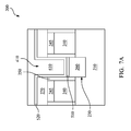
- the metal layer 610 may be recessed, as well as the adhesion layer 520 over the dielectric layer 270 , to provide a planar topography for subsequent processes, such as a lithography process, as shown in FIG. 8A (in conjunction with the process described with respect to FIG. 7A ).
- a CMP process is performed to remove excessive the metal layer 610 and the adhesion layer 520 .
- the remaining metal layer 610 in the contact trench 410 forms a contact metal 615 .
- the contact metal 615 has an upper portion 615 U and a lower portion 615 L, as shown in FIG. 8B .
- a width of the upper portion 615 U is greater than the lower portion 615 L.
- Additional steps can be provided before, during, and after the method 100 , and some of the steps described can be replaced, eliminated, or moved around for additional embodiments of the method 100 .
- the semiconductor devices, 200 may include additional features, which may be formed by subsequent processing.
- various vias/lines and multilayers interconnect features e.g., metal layers and interlayer dielectrics
- a multilayer interconnection includes vertical interconnects, such as conventional vias or contacts, and horizontal interconnects, such as metal lines.
- the various interconnection features may implement various conductive materials including copper, tungsten, and/or silicide.
- a damascene and/or dual damascene process is used to form a copper related multilayer interconnection structure.
- the present disclosure provide methods of forming a cobalt contact metal.
- the method Prior to forming the Cobalt layer with in a contact trench, the method employs forming a thin ALD TiN to enhance adhesion ability and improve electromigration resistance.
- the method provides a robust butted contact metal formation process to reduce contact resistance.
- a method for fabricating a semiconductor device includes forming a source/drain feature over a substrate, forming a dielectric layer over the source/drain feature, forming a contact trench through the dielectric layer to expose the source/drain feature, depositing a titanium nitride (TiN) layer by a first atomic layer deposition (ALD) process in the contact trench and depositing a cobalt layer over the TiN layer in the contact trench.
- TiN titanium nitride
- ALD first atomic layer deposition
- a method in yet another embodiment, includes forming a first gate stack and a second gate stack over a substrate, forming a source/drain feature over the substrate.
- the source/drain feature is disposed between the first and second gate stacks.
- the method also includes forming a dielectric layer over the source/drain feature, forming a contact trench through the dielectric layer to expose the source/drain feature, forming a self-aligned silicide layer over the exposed source/drain feature and depositing a titanium nitride (TiN) layer by a first atomic layer deposition (ALD) process in the contact trench, including over the self-aligned silicide layer.
- the method also includes depositing a cobalt layer over the TiN layer in the contact trench.
- a semiconductor device in yet another embodiment, includes forming a dielectric layer over a substrate, forming a trench in the dielectric layer, forming a titanium nitride layer by a first atomic layer deposition (ALD) process in the trench and forming a cobalt layer over the titanium nitride layer.
- ALD first atomic layer deposition
Landscapes
- Engineering & Computer Science (AREA)
- Physics & Mathematics (AREA)
- Condensed Matter Physics & Semiconductors (AREA)
- General Physics & Mathematics (AREA)
- Manufacturing & Machinery (AREA)
- Computer Hardware Design (AREA)
- Microelectronics & Electronic Packaging (AREA)
- Power Engineering (AREA)
- Electrodes Of Semiconductors (AREA)
- Insulated Gate Type Field-Effect Transistor (AREA)
Abstract
Description
Claims (21)
Priority Applications (9)
| Application Number | Priority Date | Filing Date | Title |
|---|---|---|---|
| US15/063,905 US9711402B1 (en) | 2016-03-08 | 2016-03-08 | Method of forming contact metal |
| CN202211159869.1A CN115394717A (en) | 2016-03-08 | 2016-10-28 | Method for forming semiconductor device |
| CN201610996710.3A CN107170706A (en) | 2016-03-08 | 2016-10-28 | Method for forming semiconductor device |
| TW105135667A TWI713145B (en) | 2016-03-08 | 2016-11-03 | Semiconductor devices and methods of forming the same |
| US15/628,267 US10418279B2 (en) | 2016-03-08 | 2017-06-20 | Method of forming contact metal |
| US16/571,536 US11232985B2 (en) | 2016-03-08 | 2019-09-16 | Method of forming contact metal |
| US17/580,904 US11791208B2 (en) | 2016-03-08 | 2022-01-21 | Method of forming contact metal |
| US18/360,587 US12211747B2 (en) | 2016-03-08 | 2023-07-27 | Method of forming contact metal |
| US19/027,412 US20250167047A1 (en) | 2016-03-08 | 2025-01-17 | Method of Forming Contact Metal |
Applications Claiming Priority (1)
| Application Number | Priority Date | Filing Date | Title |
|---|---|---|---|
| US15/063,905 US9711402B1 (en) | 2016-03-08 | 2016-03-08 | Method of forming contact metal |
Related Child Applications (1)
| Application Number | Title | Priority Date | Filing Date |
|---|---|---|---|
| US15/628,267 Continuation US10418279B2 (en) | 2016-03-08 | 2017-06-20 | Method of forming contact metal |
Publications (1)
| Publication Number | Publication Date |
|---|---|
| US9711402B1 true US9711402B1 (en) | 2017-07-18 |
Family
ID=59296486
Family Applications (6)
| Application Number | Title | Priority Date | Filing Date |
|---|---|---|---|
| US15/063,905 Active US9711402B1 (en) | 2016-03-08 | 2016-03-08 | Method of forming contact metal |
| US15/628,267 Active 2036-08-24 US10418279B2 (en) | 2016-03-08 | 2017-06-20 | Method of forming contact metal |
| US16/571,536 Active 2036-04-01 US11232985B2 (en) | 2016-03-08 | 2019-09-16 | Method of forming contact metal |
| US17/580,904 Active US11791208B2 (en) | 2016-03-08 | 2022-01-21 | Method of forming contact metal |
| US18/360,587 Active US12211747B2 (en) | 2016-03-08 | 2023-07-27 | Method of forming contact metal |
| US19/027,412 Pending US20250167047A1 (en) | 2016-03-08 | 2025-01-17 | Method of Forming Contact Metal |
Family Applications After (5)
| Application Number | Title | Priority Date | Filing Date |
|---|---|---|---|
| US15/628,267 Active 2036-08-24 US10418279B2 (en) | 2016-03-08 | 2017-06-20 | Method of forming contact metal |
| US16/571,536 Active 2036-04-01 US11232985B2 (en) | 2016-03-08 | 2019-09-16 | Method of forming contact metal |
| US17/580,904 Active US11791208B2 (en) | 2016-03-08 | 2022-01-21 | Method of forming contact metal |
| US18/360,587 Active US12211747B2 (en) | 2016-03-08 | 2023-07-27 | Method of forming contact metal |
| US19/027,412 Pending US20250167047A1 (en) | 2016-03-08 | 2025-01-17 | Method of Forming Contact Metal |
Country Status (3)
| Country | Link |
|---|---|
| US (6) | US9711402B1 (en) |
| CN (2) | CN115394717A (en) |
| TW (1) | TWI713145B (en) |
Cited By (1)
| Publication number | Priority date | Publication date | Assignee | Title |
|---|---|---|---|---|
| US11205703B2 (en) * | 2019-07-08 | 2021-12-21 | Semiconductor Manufacturing International (Shanghai) Corporation | Semiconductor device and fabrication method thereof |
Families Citing this family (2)
| Publication number | Priority date | Publication date | Assignee | Title |
|---|---|---|---|---|
| US9711402B1 (en) | 2016-03-08 | 2017-07-18 | Taiwan Semiconductor Manufacturing Company, Ltd. | Method of forming contact metal |
| DE102018102448B4 (en) * | 2017-11-30 | 2023-06-15 | Taiwan Semiconductor Manufacturing Co., Ltd. | Formation and structure of conductive features |
Citations (32)
| Publication number | Priority date | Publication date | Assignee | Title |
|---|---|---|---|---|
| US5858875A (en) * | 1995-02-03 | 1999-01-12 | National Semiconductor Corporation | Integrated circuits with borderless vias |
| US20020068429A1 (en) * | 1999-09-01 | 2002-06-06 | Micron Technology, Inc. | Local interconnect structures and methods for making the same |
| US20070069385A1 (en) * | 2005-09-13 | 2007-03-29 | Anthony Oates | MIM capacitor integrated into the damascene structure and method of making thereof |
| US20080296666A1 (en) * | 2007-06-04 | 2008-12-04 | Elpida Memory, Inc. | Semiconductor device including an embedded contact plug |
| US7473637B2 (en) * | 2005-07-20 | 2009-01-06 | Micron Technology, Inc. | ALD formed titanium nitride films |
| US7667271B2 (en) | 2007-04-27 | 2010-02-23 | Taiwan Semiconductor Manufacturing Company, Ltd. | Fin field-effect transistors |
| US20100155846A1 (en) * | 2008-12-19 | 2010-06-24 | Niloy Mukherjee | Metal-insulator-semiconductor tunneling contacts |
| US7910453B2 (en) | 2008-07-14 | 2011-03-22 | Taiwan Semiconductor Manufacturing Company, Ltd. | Storage nitride encapsulation for non-planar sonos NAND flash charge retention |
| US20120139015A1 (en) * | 2010-12-07 | 2012-06-07 | GlobalFoundries, Inc. | Metal semiconductor alloy contact with low resistance |
| US20120329234A1 (en) * | 2011-06-22 | 2012-12-27 | Porter Jason T | Method for forming a semiconductor device having a cobalt silicide |
| US8377779B1 (en) | 2012-01-03 | 2013-02-19 | Taiwan Semiconductor Manufacturing Company, Ltd. | Methods of manufacturing semiconductor devices and transistors |
| US8399931B2 (en) | 2010-06-30 | 2013-03-19 | Taiwan Semiconductor Manufacturing Company, Ltd. | Layout for multiple-fin SRAM cell |
| US20130175626A1 (en) * | 2012-01-06 | 2013-07-11 | International Business Machines Corporation | Integrated circuit having raised source drains devices with reduced silicide contact resistance and methods to fabricate same |
| US20140001520A1 (en) * | 2012-06-29 | 2014-01-02 | Glenn A. Glass | Contact resistance reduced p-mos transistors employing ge-rich contact layer |
| US20140001574A1 (en) | 2011-09-08 | 2014-01-02 | Taiwan Semiconductor Manufacturing Company, Ltd. | Improved silicide formation and associated devices |
| US8652894B2 (en) | 2010-02-11 | 2014-02-18 | Taiwan Semiconductor Manufacturing Company, Ltd. | Method for fabricating a FinFET device |
| US20140110755A1 (en) | 2012-10-24 | 2014-04-24 | Taiwan Semiconductor Manufacturing Company, Ltd. | Apparatus and Method for Forming Semiconductor Contacts |
| US8716765B2 (en) | 2012-03-23 | 2014-05-06 | Taiwan Semiconductor Manufacturing Company, Ltd. | Contact structure of semiconductor device |
| US20140124842A1 (en) * | 2012-11-08 | 2014-05-08 | Taiwan Semiconductor Manufacturing Company, Ltd. | Contact Structure of Semiconductor Device |
| US8723272B2 (en) | 2011-10-04 | 2014-05-13 | Taiwan Semiconductor Manufacturing Company, Ltd. | FinFET device and method of manufacturing same |
| US8729627B2 (en) | 2010-05-14 | 2014-05-20 | Taiwan Semiconductor Manufacturing Company, Ltd. | Strained channel integrated circuit devices |
| US8735993B2 (en) | 2012-01-31 | 2014-05-27 | Taiwan Semiconductor Manufacturing Company, Ltd. | FinFET body contact and method of making same |
| US8736056B2 (en) | 2012-07-31 | 2014-05-27 | Taiwan Semiconductor Manufacturing Company, Ltd. | Device for reducing contact resistance of a metal |
| US20140151812A1 (en) | 2012-11-30 | 2014-06-05 | Taiwan Semiconductor Manufacturing Company, Ltd. | Contact Plugs in SRAM Cells and the Method of Forming the Same |
| US20140183645A1 (en) * | 2012-12-28 | 2014-07-03 | Taiwan Semiconductor Manufacturing Company, Ltd. | Complimentary Metal-Oxide-Semiconductor (CMOS) With Low Contact Resistivity and Method of Forming Same |
| US8785285B2 (en) | 2012-03-08 | 2014-07-22 | Taiwan Semiconductor Manufacturing Company, Ltd. | Semiconductor devices and methods of manufacture thereof |
| US8816444B2 (en) | 2011-04-29 | 2014-08-26 | Taiwan Semiconductor Manufacturing Company, Ltd. | System and methods for converting planar design to FinFET design |
| US8860148B2 (en) | 2012-04-11 | 2014-10-14 | Taiwan Semiconductor Manufacturing Company, Ltd. | Structure and method for FinFET integrated with capacitor |
| US20150279970A1 (en) * | 2014-03-31 | 2015-10-01 | Stmicroelctronics, Inc. | Soi finfet transistor with strained channel |
| US9219062B2 (en) * | 2013-05-24 | 2015-12-22 | GlobalFoundries, Inc. | Integrated circuits with improved source/drain contacts and methods for fabricating such integrated circuits |
| US9373680B1 (en) * | 2015-02-02 | 2016-06-21 | Globalfoundries Inc. | Integrated circuits with capacitors and methods of producing the same |
| US9396995B1 (en) * | 2015-02-27 | 2016-07-19 | Globalfoundries Inc. | MOL contact metallization scheme for improved yield and device reliability |
Family Cites Families (38)
| Publication number | Priority date | Publication date | Assignee | Title |
|---|---|---|---|---|
| DE3138705A1 (en) * | 1981-09-29 | 1983-04-07 | Siemens AG, 1000 Berlin und 8000 München | "ELECTROCHROMIC DISPLAY" |
| JPH0950986A (en) * | 1995-05-29 | 1997-02-18 | Sony Corp | Forming connection holes |
| TW412640B (en) * | 1998-02-24 | 2000-11-21 | Asahi Glass Co Ltd | Light absorption antireflective body and method of producing the same |
| TW382787B (en) * | 1998-10-02 | 2000-02-21 | United Microelectronics Corp | Method of fabricating dual damascene |
| US6211048B1 (en) * | 1998-12-21 | 2001-04-03 | United Microelectronics Corp. | Method of reducing salicide lateral growth |
| US8994104B2 (en) * | 1999-09-28 | 2015-03-31 | Intel Corporation | Contact resistance reduction employing germanium overlayer pre-contact metalization |
| US6727169B1 (en) * | 1999-10-15 | 2004-04-27 | Asm International, N.V. | Method of making conformal lining layers for damascene metallization |
| KR100363088B1 (en) * | 2000-04-20 | 2002-12-02 | 삼성전자 주식회사 | Method of manufacturing barrier metal layer using atomic layer deposition method |
| US6399490B1 (en) * | 2000-06-29 | 2002-06-04 | International Business Machines Corporation | Highly conformal titanium nitride deposition process for high aspect ratio structures |
| KR100343653B1 (en) * | 2000-09-22 | 2002-07-11 | 윤종용 | Semiconductor device with metal silicide layer and method of manufacturing the same |
| JP2002319551A (en) * | 2001-04-23 | 2002-10-31 | Nec Corp | Semiconductor device and manufacturing method thereof |
| US6667510B2 (en) * | 2002-02-19 | 2003-12-23 | Silicon Based Technology Corp. | Self-aligned split-gate flash memory cell and its contactless memory array |
| US6776185B2 (en) * | 2002-07-03 | 2004-08-17 | Delphi Technologies, Inc. | Grounded jet pump assembly for fuel system |
| KR100467021B1 (en) * | 2002-08-20 | 2005-01-24 | 삼성전자주식회사 | Contact structure of semiconductro device and method for fabricating the same |
| CN1627504A (en) * | 2003-12-12 | 2005-06-15 | 南亚科技股份有限公司 | Method for improving contact resistance value of bit line |
| KR100615237B1 (en) * | 2004-08-07 | 2006-08-25 | 삼성에스디아이 주식회사 | Thin film transistor and method of manufacturing same |
| TW200847404A (en) * | 2007-05-18 | 2008-12-01 | Nanya Technology Corp | Flash memory device and method for fabricating thereof |
| US7622354B2 (en) * | 2007-08-31 | 2009-11-24 | Qimonda Ag | Integrated circuit and method of manufacturing an integrated circuit |
| JP2010080798A (en) * | 2008-09-29 | 2010-04-08 | Renesas Technology Corp | Semiconductor integrated circuit device and method of manufacturing the same |
| US7863123B2 (en) * | 2009-01-19 | 2011-01-04 | International Business Machines Corporation | Direct contact between high-κ/metal gate and wiring process flow |
| US8435851B2 (en) | 2011-01-12 | 2013-05-07 | International Business Machines Corporation | Implementing semiconductor SoC with metal via gate node high performance stacked transistors |
| US8507350B2 (en) * | 2011-09-21 | 2013-08-13 | United Microelectronics Corporation | Fabricating method of semiconductor elements |
| US8975672B2 (en) * | 2011-11-09 | 2015-03-10 | United Microelectronics Corp. | Metal oxide semiconductor transistor and manufacturing method thereof |
| EP2779224A3 (en) * | 2013-03-15 | 2014-12-31 | Applied Materials, Inc. | Methods for producing interconnects in semiconductor devices |
| US20150008488A1 (en) * | 2013-07-02 | 2015-01-08 | Stmicroelectronics, Inc. | Uniform height replacement metal gate |
| US20150372143A1 (en) * | 2014-06-20 | 2015-12-24 | Samsung Electronics Co., Ltd. | Semiconductor device and method for fabricating the same |
| US9595524B2 (en) * | 2014-07-15 | 2017-03-14 | Globalfoundries Inc. | FinFET source-drain merged by silicide-based material |
| US9716160B2 (en) * | 2014-08-01 | 2017-07-25 | International Business Machines Corporation | Extended contact area using undercut silicide extensions |
| US10297673B2 (en) * | 2014-10-08 | 2019-05-21 | Samsung Electronics Co., Ltd. | Methods of forming semiconductor devices including conductive contacts on source/drains |
| US9761691B2 (en) * | 2014-12-04 | 2017-09-12 | GlobalFoundries, Inc. | Integrated circuits including replacement gate structures and methods for fabricating the same |
| US9570348B2 (en) * | 2015-05-11 | 2017-02-14 | United Microelectronics Corp. | Method of forming contact strucutre |
| US9627498B2 (en) * | 2015-05-20 | 2017-04-18 | Macronix International Co., Ltd. | Contact structure for thin film semiconductor |
| WO2016209285A1 (en) * | 2015-06-26 | 2016-12-29 | Intel Corporation | Pseudomorphic ingaas on gaas for gate-all-around transistors |
| EP3353813B1 (en) * | 2015-09-25 | 2024-06-05 | Intel Corporation | Semiconductor device contacts with increased contact area |
| US9755078B2 (en) * | 2015-10-23 | 2017-09-05 | International Business Machines Corporation | Structure and method for multi-threshold voltage adjusted silicon germanium alloy devices with same silicon germanium content |
| US9583612B1 (en) * | 2016-01-21 | 2017-02-28 | Texas Instruments Incorporated | Drift region implant self-aligned to field relief oxide with sidewall dielectric |
| US10153351B2 (en) * | 2016-01-29 | 2018-12-11 | Taiwan Semiconductor Manufacturing Co., Ltd. | Semiconductor device and a method for fabricating the same |
| US9711402B1 (en) | 2016-03-08 | 2017-07-18 | Taiwan Semiconductor Manufacturing Company, Ltd. | Method of forming contact metal |
-
2016
- 2016-03-08 US US15/063,905 patent/US9711402B1/en active Active
- 2016-10-28 CN CN202211159869.1A patent/CN115394717A/en active Pending
- 2016-10-28 CN CN201610996710.3A patent/CN107170706A/en active Pending
- 2016-11-03 TW TW105135667A patent/TWI713145B/en active
-
2017
- 2017-06-20 US US15/628,267 patent/US10418279B2/en active Active
-
2019
- 2019-09-16 US US16/571,536 patent/US11232985B2/en active Active
-
2022
- 2022-01-21 US US17/580,904 patent/US11791208B2/en active Active
-
2023
- 2023-07-27 US US18/360,587 patent/US12211747B2/en active Active
-
2025
- 2025-01-17 US US19/027,412 patent/US20250167047A1/en active Pending
Patent Citations (35)
| Publication number | Priority date | Publication date | Assignee | Title |
|---|---|---|---|---|
| US5858875A (en) * | 1995-02-03 | 1999-01-12 | National Semiconductor Corporation | Integrated circuits with borderless vias |
| US20020068429A1 (en) * | 1999-09-01 | 2002-06-06 | Micron Technology, Inc. | Local interconnect structures and methods for making the same |
| US7473637B2 (en) * | 2005-07-20 | 2009-01-06 | Micron Technology, Inc. | ALD formed titanium nitride films |
| US20070069385A1 (en) * | 2005-09-13 | 2007-03-29 | Anthony Oates | MIM capacitor integrated into the damascene structure and method of making thereof |
| US7667271B2 (en) | 2007-04-27 | 2010-02-23 | Taiwan Semiconductor Manufacturing Company, Ltd. | Fin field-effect transistors |
| US20080296666A1 (en) * | 2007-06-04 | 2008-12-04 | Elpida Memory, Inc. | Semiconductor device including an embedded contact plug |
| US7910453B2 (en) | 2008-07-14 | 2011-03-22 | Taiwan Semiconductor Manufacturing Company, Ltd. | Storage nitride encapsulation for non-planar sonos NAND flash charge retention |
| US20100155846A1 (en) * | 2008-12-19 | 2010-06-24 | Niloy Mukherjee | Metal-insulator-semiconductor tunneling contacts |
| US8652894B2 (en) | 2010-02-11 | 2014-02-18 | Taiwan Semiconductor Manufacturing Company, Ltd. | Method for fabricating a FinFET device |
| US8729627B2 (en) | 2010-05-14 | 2014-05-20 | Taiwan Semiconductor Manufacturing Company, Ltd. | Strained channel integrated circuit devices |
| US8399931B2 (en) | 2010-06-30 | 2013-03-19 | Taiwan Semiconductor Manufacturing Company, Ltd. | Layout for multiple-fin SRAM cell |
| US20120139015A1 (en) * | 2010-12-07 | 2012-06-07 | GlobalFoundries, Inc. | Metal semiconductor alloy contact with low resistance |
| US8816444B2 (en) | 2011-04-29 | 2014-08-26 | Taiwan Semiconductor Manufacturing Company, Ltd. | System and methods for converting planar design to FinFET design |
| US20120329234A1 (en) * | 2011-06-22 | 2012-12-27 | Porter Jason T | Method for forming a semiconductor device having a cobalt silicide |
| US8686516B2 (en) | 2011-09-08 | 2014-04-01 | Taiwan Semiconductor Manufacturing Company, Ltd. | Silicide formation and associated devices |
| US20140001574A1 (en) | 2011-09-08 | 2014-01-02 | Taiwan Semiconductor Manufacturing Company, Ltd. | Improved silicide formation and associated devices |
| US8723272B2 (en) | 2011-10-04 | 2014-05-13 | Taiwan Semiconductor Manufacturing Company, Ltd. | FinFET device and method of manufacturing same |
| US8377779B1 (en) | 2012-01-03 | 2013-02-19 | Taiwan Semiconductor Manufacturing Company, Ltd. | Methods of manufacturing semiconductor devices and transistors |
| US20130175626A1 (en) * | 2012-01-06 | 2013-07-11 | International Business Machines Corporation | Integrated circuit having raised source drains devices with reduced silicide contact resistance and methods to fabricate same |
| US8735993B2 (en) | 2012-01-31 | 2014-05-27 | Taiwan Semiconductor Manufacturing Company, Ltd. | FinFET body contact and method of making same |
| US8785285B2 (en) | 2012-03-08 | 2014-07-22 | Taiwan Semiconductor Manufacturing Company, Ltd. | Semiconductor devices and methods of manufacture thereof |
| US8716765B2 (en) | 2012-03-23 | 2014-05-06 | Taiwan Semiconductor Manufacturing Company, Ltd. | Contact structure of semiconductor device |
| US8860148B2 (en) | 2012-04-11 | 2014-10-14 | Taiwan Semiconductor Manufacturing Company, Ltd. | Structure and method for FinFET integrated with capacitor |
| US20140001520A1 (en) * | 2012-06-29 | 2014-01-02 | Glenn A. Glass | Contact resistance reduced p-mos transistors employing ge-rich contact layer |
| US8736056B2 (en) | 2012-07-31 | 2014-05-27 | Taiwan Semiconductor Manufacturing Company, Ltd. | Device for reducing contact resistance of a metal |
| US8772109B2 (en) | 2012-10-24 | 2014-07-08 | Taiwan Semiconductor Manufacturing Company, Ltd. | Apparatus and method for forming semiconductor contacts |
| US20140110755A1 (en) | 2012-10-24 | 2014-04-24 | Taiwan Semiconductor Manufacturing Company, Ltd. | Apparatus and Method for Forming Semiconductor Contacts |
| US20140124842A1 (en) * | 2012-11-08 | 2014-05-08 | Taiwan Semiconductor Manufacturing Company, Ltd. | Contact Structure of Semiconductor Device |
| US8823065B2 (en) | 2012-11-08 | 2014-09-02 | Taiwan Semiconductor Manufacturing Company, Ltd. | Contact structure of semiconductor device |
| US20140151812A1 (en) | 2012-11-30 | 2014-06-05 | Taiwan Semiconductor Manufacturing Company, Ltd. | Contact Plugs in SRAM Cells and the Method of Forming the Same |
| US20140183645A1 (en) * | 2012-12-28 | 2014-07-03 | Taiwan Semiconductor Manufacturing Company, Ltd. | Complimentary Metal-Oxide-Semiconductor (CMOS) With Low Contact Resistivity and Method of Forming Same |
| US9219062B2 (en) * | 2013-05-24 | 2015-12-22 | GlobalFoundries, Inc. | Integrated circuits with improved source/drain contacts and methods for fabricating such integrated circuits |
| US20150279970A1 (en) * | 2014-03-31 | 2015-10-01 | Stmicroelctronics, Inc. | Soi finfet transistor with strained channel |
| US9373680B1 (en) * | 2015-02-02 | 2016-06-21 | Globalfoundries Inc. | Integrated circuits with capacitors and methods of producing the same |
| US9396995B1 (en) * | 2015-02-27 | 2016-07-19 | Globalfoundries Inc. | MOL contact metallization scheme for improved yield and device reliability |
Cited By (2)
| Publication number | Priority date | Publication date | Assignee | Title |
|---|---|---|---|---|
| US11205703B2 (en) * | 2019-07-08 | 2021-12-21 | Semiconductor Manufacturing International (Shanghai) Corporation | Semiconductor device and fabrication method thereof |
| US11742398B2 (en) | 2019-07-08 | 2023-08-29 | Semiconductor Manufacturing International (Shanghai) Corporation | Semiconductor device with isolation between conductive structures |
Also Published As
| Publication number | Publication date |
|---|---|
| CN107170706A (en) | 2017-09-15 |
| US20200013674A1 (en) | 2020-01-09 |
| US20230386918A1 (en) | 2023-11-30 |
| US10418279B2 (en) | 2019-09-17 |
| US20250167047A1 (en) | 2025-05-22 |
| US12211747B2 (en) | 2025-01-28 |
| CN115394717A (en) | 2022-11-25 |
| US20170287779A1 (en) | 2017-10-05 |
| US11232985B2 (en) | 2022-01-25 |
| US20220148920A1 (en) | 2022-05-12 |
| US11791208B2 (en) | 2023-10-17 |
| TWI713145B (en) | 2020-12-11 |
| TW201733003A (en) | 2017-09-16 |
Similar Documents
| Publication | Publication Date | Title |
|---|---|---|
| US11610888B2 (en) | Semiconductor device having cap layer | |
| US10163720B2 (en) | Method of forming source/drain contact | |
| US12198974B2 (en) | Dielectric gap-filling process for semiconductor device | |
| US10325816B2 (en) | Structure and method for FinFET device | |
| US11145719B2 (en) | Semiconductor device having a contact | |
| US9564363B1 (en) | Method of forming butted contact | |
| US12125748B2 (en) | Contact plug | |
| US12211747B2 (en) | Method of forming contact metal | |
| US10163719B2 (en) | Method of forming self-alignment contact | |
| TWI749871B (en) | Semiconductor device and method for forming the same |
Legal Events
| Date | Code | Title | Description |
|---|---|---|---|
| AS | Assignment |
Owner name: TAIWAN SEMICONDUCTOR MANUFACTURING COMPANY, LTD., Free format text: ASSIGNMENT OF ASSIGNORS INTEREST;ASSIGNORS:HUANG, CHUN-HSIEN;LEE, HONG-MAO;LIN, WEI-JUNG;AND OTHERS;REEL/FRAME:037921/0265 Effective date: 20160302 |
|
| STCF | Information on status: patent grant |
Free format text: PATENTED CASE |
|
| MAFP | Maintenance fee payment |
Free format text: PAYMENT OF MAINTENANCE FEE, 4TH YEAR, LARGE ENTITY (ORIGINAL EVENT CODE: M1551); ENTITY STATUS OF PATENT OWNER: LARGE ENTITY Year of fee payment: 4 |
|
| MAFP | Maintenance fee payment |
Free format text: PAYMENT OF MAINTENANCE FEE, 8TH YEAR, LARGE ENTITY (ORIGINAL EVENT CODE: M1552); ENTITY STATUS OF PATENT OWNER: LARGE ENTITY Year of fee payment: 8 |