US9240325B2 - Method for making an integrated circuit - Google Patents
Method for making an integrated circuit Download PDFInfo
- Publication number
- US9240325B2 US9240325B2 US14/498,091 US201414498091A US9240325B2 US 9240325 B2 US9240325 B2 US 9240325B2 US 201414498091 A US201414498091 A US 201414498091A US 9240325 B2 US9240325 B2 US 9240325B2
- Authority
- US
- United States
- Prior art keywords
- layer
- metal
- gate
- zones
- zone
- Prior art date
- Legal status (The legal status is an assumption and is not a legal conclusion. Google has not performed a legal analysis and makes no representation as to the accuracy of the status listed.)
- Active
Links
Images


Classifications
-
- H—ELECTRICITY
- H10—SEMICONDUCTOR DEVICES; ELECTRIC SOLID-STATE DEVICES NOT OTHERWISE PROVIDED FOR
- H10D—INORGANIC ELECTRIC SEMICONDUCTOR DEVICES
- H10D64/00—Electrodes of devices having potential barriers
- H10D64/20—Electrodes characterised by their shapes, relative sizes or dispositions
- H10D64/27—Electrodes not carrying the current to be rectified, amplified, oscillated or switched, e.g. gates
- H10D64/311—Gate electrodes for field-effect devices
- H10D64/411—Gate electrodes for field-effect devices for FETs
- H10D64/511—Gate electrodes for field-effect devices for FETs for IGFETs
- H10D64/517—Gate electrodes for field-effect devices for FETs for IGFETs characterised by the conducting layers
-
- H—ELECTRICITY
- H01—ELECTRIC ELEMENTS
- H01L—SEMICONDUCTOR DEVICES NOT COVERED BY CLASS H10
- H01L21/00—Processes or apparatus adapted for the manufacture or treatment of semiconductor or solid state devices or of parts thereof
- H01L21/02—Manufacture or treatment of semiconductor devices or of parts thereof
- H01L21/04—Manufacture or treatment of semiconductor devices or of parts thereof the devices having potential barriers, e.g. a PN junction, depletion layer or carrier concentration layer
- H01L21/18—Manufacture or treatment of semiconductor devices or of parts thereof the devices having potential barriers, e.g. a PN junction, depletion layer or carrier concentration layer the devices having semiconductor bodies comprising elements of Group IV of the Periodic Table or AIIIBV compounds with or without impurities, e.g. doping materials
- H01L21/28—Manufacture of electrodes on semiconductor bodies using processes or apparatus not provided for in groups H01L21/20 - H01L21/268
- H01L21/28008—Making conductor-insulator-semiconductor electrodes
- H01L21/28017—Making conductor-insulator-semiconductor electrodes the insulator being formed after the semiconductor body, the semiconductor being silicon
- H01L21/28026—Making conductor-insulator-semiconductor electrodes the insulator being formed after the semiconductor body, the semiconductor being silicon characterised by the conductor
- H01L21/28035—Making conductor-insulator-semiconductor electrodes the insulator being formed after the semiconductor body, the semiconductor being silicon characterised by the conductor the final conductor layer next to the insulator being silicon, e.g. polysilicon, with or without impurities
- H01L21/28044—Making conductor-insulator-semiconductor electrodes the insulator being formed after the semiconductor body, the semiconductor being silicon characterised by the conductor the final conductor layer next to the insulator being silicon, e.g. polysilicon, with or without impurities the conductor comprising at least another non-silicon conductive layer
- H01L21/28052—Making conductor-insulator-semiconductor electrodes the insulator being formed after the semiconductor body, the semiconductor being silicon characterised by the conductor the final conductor layer next to the insulator being silicon, e.g. polysilicon, with or without impurities the conductor comprising at least another non-silicon conductive layer the conductor comprising a silicide layer formed by the silicidation reaction of silicon with a metal layer
-
- H—ELECTRICITY
- H01—ELECTRIC ELEMENTS
- H01L—SEMICONDUCTOR DEVICES NOT COVERED BY CLASS H10
- H01L21/00—Processes or apparatus adapted for the manufacture or treatment of semiconductor or solid state devices or of parts thereof
- H01L21/02—Manufacture or treatment of semiconductor devices or of parts thereof
- H01L21/04—Manufacture or treatment of semiconductor devices or of parts thereof the devices having potential barriers, e.g. a PN junction, depletion layer or carrier concentration layer
- H01L21/18—Manufacture or treatment of semiconductor devices or of parts thereof the devices having potential barriers, e.g. a PN junction, depletion layer or carrier concentration layer the devices having semiconductor bodies comprising elements of Group IV of the Periodic Table or AIIIBV compounds with or without impurities, e.g. doping materials
- H01L21/28—Manufacture of electrodes on semiconductor bodies using processes or apparatus not provided for in groups H01L21/20 - H01L21/268
- H01L21/28008—Making conductor-insulator-semiconductor electrodes
- H01L21/28017—Making conductor-insulator-semiconductor electrodes the insulator being formed after the semiconductor body, the semiconductor being silicon
- H01L21/28026—Making conductor-insulator-semiconductor electrodes the insulator being formed after the semiconductor body, the semiconductor being silicon characterised by the conductor
- H01L21/28123—Lithography-related aspects, e.g. sub-lithography lengths; Isolation-related aspects, e.g. to solve problems arising at the crossing with the side of the device isolation; Planarisation aspects
-
- H—ELECTRICITY
- H01—ELECTRIC ELEMENTS
- H01L—SEMICONDUCTOR DEVICES NOT COVERED BY CLASS H10
- H01L21/00—Processes or apparatus adapted for the manufacture or treatment of semiconductor or solid state devices or of parts thereof
- H01L21/02—Manufacture or treatment of semiconductor devices or of parts thereof
- H01L21/04—Manufacture or treatment of semiconductor devices or of parts thereof the devices having potential barriers, e.g. a PN junction, depletion layer or carrier concentration layer
- H01L21/18—Manufacture or treatment of semiconductor devices or of parts thereof the devices having potential barriers, e.g. a PN junction, depletion layer or carrier concentration layer the devices having semiconductor bodies comprising elements of Group IV of the Periodic Table or AIIIBV compounds with or without impurities, e.g. doping materials
- H01L21/28—Manufacture of electrodes on semiconductor bodies using processes or apparatus not provided for in groups H01L21/20 - H01L21/268
- H01L21/283—Deposition of conductive or insulating materials for electrodes conducting electric current
-
- H01L29/42372—
-
- H01L29/49—
-
- H01L29/4933—
-
- H01L29/4975—
-
- H01L29/66507—
-
- H01L29/6653—
-
- H01L29/66545—
-
- H01L29/78—
-
- H—ELECTRICITY
- H10—SEMICONDUCTOR DEVICES; ELECTRIC SOLID-STATE DEVICES NOT OTHERWISE PROVIDED FOR
- H10D—INORGANIC ELECTRIC SEMICONDUCTOR DEVICES
- H10D30/00—Field-effect transistors [FET]
- H10D30/01—Manufacture or treatment
- H10D30/021—Manufacture or treatment of FETs having insulated gates [IGFET]
- H10D30/0212—Manufacture or treatment of FETs having insulated gates [IGFET] using self-aligned silicidation
- H10D30/0213—Manufacture or treatment of FETs having insulated gates [IGFET] using self-aligned silicidation providing different silicide thicknesses on gate electrodes and on source regions or drain regions
-
- H—ELECTRICITY
- H10—SEMICONDUCTOR DEVICES; ELECTRIC SOLID-STATE DEVICES NOT OTHERWISE PROVIDED FOR
- H10D—INORGANIC ELECTRIC SEMICONDUCTOR DEVICES
- H10D30/00—Field-effect transistors [FET]
- H10D30/60—Insulated-gate field-effect transistors [IGFET]
-
- H—ELECTRICITY
- H10—SEMICONDUCTOR DEVICES; ELECTRIC SOLID-STATE DEVICES NOT OTHERWISE PROVIDED FOR
- H10D—INORGANIC ELECTRIC SEMICONDUCTOR DEVICES
- H10D62/00—Semiconductor bodies, or regions thereof, of devices having potential barriers
- H10D62/10—Shapes, relative sizes or dispositions of the regions of the semiconductor bodies; Shapes of the semiconductor bodies
- H10D62/113—Isolations within a component, i.e. internal isolations
- H10D62/115—Dielectric isolations, e.g. air gaps
-
- H10D64/013—
-
- H10D64/0131—
-
- H10D64/01326—
-
- H—ELECTRICITY
- H10—SEMICONDUCTOR DEVICES; ELECTRIC SOLID-STATE DEVICES NOT OTHERWISE PROVIDED FOR
- H10D—INORGANIC ELECTRIC SEMICONDUCTOR DEVICES
- H10D64/00—Electrodes of devices having potential barriers
- H10D64/01—Manufacture or treatment
- H10D64/015—Manufacture or treatment removing at least parts of gate spacers, e.g. disposable spacers
-
- H—ELECTRICITY
- H10—SEMICONDUCTOR DEVICES; ELECTRIC SOLID-STATE DEVICES NOT OTHERWISE PROVIDED FOR
- H10D—INORGANIC ELECTRIC SEMICONDUCTOR DEVICES
- H10D64/00—Electrodes of devices having potential barriers
- H10D64/01—Manufacture or treatment
- H10D64/017—Manufacture or treatment using dummy gates in processes wherein at least parts of the final gates are self-aligned to the dummy gates, i.e. replacement gate processes
-
- H—ELECTRICITY
- H10—SEMICONDUCTOR DEVICES; ELECTRIC SOLID-STATE DEVICES NOT OTHERWISE PROVIDED FOR
- H10D—INORGANIC ELECTRIC SEMICONDUCTOR DEVICES
- H10D64/00—Electrodes of devices having potential barriers
- H10D64/60—Electrodes characterised by their materials
- H10D64/62—Electrodes ohmically coupled to a semiconductor
-
- H—ELECTRICITY
- H10—SEMICONDUCTOR DEVICES; ELECTRIC SOLID-STATE DEVICES NOT OTHERWISE PROVIDED FOR
- H10D—INORGANIC ELECTRIC SEMICONDUCTOR DEVICES
- H10D64/00—Electrodes of devices having potential barriers
- H10D64/60—Electrodes characterised by their materials
- H10D64/66—Electrodes having a conductor capacitively coupled to a semiconductor by an insulator, e.g. MIS electrodes
- H10D64/661—Electrodes having a conductor capacitively coupled to a semiconductor by an insulator, e.g. MIS electrodes the conductor comprising a layer of silicon contacting the insulator, e.g. polysilicon having vertical doping variation
- H10D64/662—Electrodes having a conductor capacitively coupled to a semiconductor by an insulator, e.g. MIS electrodes the conductor comprising a layer of silicon contacting the insulator, e.g. polysilicon having vertical doping variation the conductor further comprising additional layers, e.g. multiple silicon layers having different crystal structures
- H10D64/663—Electrodes having a conductor capacitively coupled to a semiconductor by an insulator, e.g. MIS electrodes the conductor comprising a layer of silicon contacting the insulator, e.g. polysilicon having vertical doping variation the conductor further comprising additional layers, e.g. multiple silicon layers having different crystal structures the additional layers comprising a silicide layer contacting the layer of silicon, e.g. polycide gates
-
- H—ELECTRICITY
- H10—SEMICONDUCTOR DEVICES; ELECTRIC SOLID-STATE DEVICES NOT OTHERWISE PROVIDED FOR
- H10D—INORGANIC ELECTRIC SEMICONDUCTOR DEVICES
- H10D64/00—Electrodes of devices having potential barriers
- H10D64/60—Electrodes characterised by their materials
- H10D64/66—Electrodes having a conductor capacitively coupled to a semiconductor by an insulator, e.g. MIS electrodes
- H10D64/667—Electrodes having a conductor capacitively coupled to a semiconductor by an insulator, e.g. MIS electrodes the conductor comprising a layer of alloy material, compound material or organic material contacting the insulator, e.g. TiN workfunction layers
- H10D64/668—Electrodes having a conductor capacitively coupled to a semiconductor by an insulator, e.g. MIS electrodes the conductor comprising a layer of alloy material, compound material or organic material contacting the insulator, e.g. TiN workfunction layers the layer being a silicide, e.g. TiSi2
-
- H—ELECTRICITY
- H10—SEMICONDUCTOR DEVICES; ELECTRIC SOLID-STATE DEVICES NOT OTHERWISE PROVIDED FOR
- H10D—INORGANIC ELECTRIC SEMICONDUCTOR DEVICES
- H10D84/00—Integrated devices formed in or on semiconductor substrates that comprise only semiconducting layers, e.g. on Si wafers or on GaAs-on-Si wafers
- H10D84/80—Integrated devices formed in or on semiconductor substrates that comprise only semiconducting layers, e.g. on Si wafers or on GaAs-on-Si wafers characterised by the integration of at least one component covered by groups H10D12/00 or H10D30/00, e.g. integration of IGFETs
- H10D84/82—Integrated devices formed in or on semiconductor substrates that comprise only semiconducting layers, e.g. on Si wafers or on GaAs-on-Si wafers characterised by the integration of at least one component covered by groups H10D12/00 or H10D30/00, e.g. integration of IGFETs of only field-effect components
- H10D84/83—Integrated devices formed in or on semiconductor substrates that comprise only semiconducting layers, e.g. on Si wafers or on GaAs-on-Si wafers characterised by the integration of at least one component covered by groups H10D12/00 or H10D30/00, e.g. integration of IGFETs of only field-effect components of only insulated-gate FETs [IGFET]
-
- H10P14/40—
Definitions
- the technical field of the invention is that of methods for making integrated circuits.
- the present invention relates to a method for making a transistor and in particular a method for making a transistor with self-aligned contacts using a “gate-first” approach.
- SOI silicon on insulator
- a method for making a transistor with a “gate-last” type approach comprises a step for making a gate zone within a sacrificial stack, then a step for replacing the sacrificial stack with the final gate stack.
- Another possible approach is the “gate-first” approach.
- a gate zone is made directly in a gate stack, which will make up the gate zone in the final integrated circuit.
- a “gate-first” approach does not require the use of sacrificial materials and is therefore beneficially less costly to implement than a “gate-last” approach.
- SOI technology favours “gate-first” type approaches in the manufacture of components, since the specifications in terms of threshold voltage are slightly less restrictive than in “bulk” type approaches.
- FIGS. 1 to 12 A method 100 for making MOSFET transistors with self-aligned contacts in a “gate-first” approach in accordance with the state of the art is described, for example, in FIGS. 1 to 12 .
- FIGS. 1 to 12 are described jointly.
- a first step 101 in the method 100 is shown in sectional view in FIG. 1 a and in a top view in FIG. 1 b .
- the sectional view is along a first plane P 1 with centre O and orthogonal axes X and Z; the top view is along a second plane P 2 of centre O and orthogonal axes X and Y.
- the second plane P 2 is perpendicular to the first plane P 1 .
- a start is made from a substrate 10 of the SOI type which incorporates shallow trench insulation (STI).
- the substrate 10 comprises a first layer 11 of Si, on which an insulating layer 12 of SiO2 extends, also known as Box (“buried oxide”).
- the insulating layer 12 has a thickness measured along the Z axis which is typically less than or equal to 25 nm.
- a thin layer 13 of Si extends over the insulating layer 12 .
- the thin layer 13 of Si has a thickness measured along the Z axis which is typically less than 5 nm.
- the thin layer 13 of Si forms an active zone.
- the substrate 10 incorporates STI insulation zones 14 .
- the substrate 10 thus has alternating insulation zones 14 and active zones 13 .
- a second step 102 of the method 100 is illustrated as a sectional view in FIG. 2 .
- the sectional view is along the first plane P 1 .
- a gate stack 15 is deposited on the substrate 10 .
- the gate stack 15 can typically comprise;
- a third step 103 in the method 100 is shown in sectional view in FIG. 3 a and in a top view in FIG. 3 b .
- the sectional view is along the first plane P 1 and the top view is along the second plane P 2 .
- gate zones 16 are defined in the gate stack 15 , for example using lithography and anisotropic etching of the gate stack 15 .
- Each gate zone 16 has, in the example shown, a width of 14 nm measured along the X axis.
- the separation distance along the X axis between two consecutive gate zones 16 is 64 nm in the example shown.
- First insulating spacers 17 are then made around each gate zone 16 .
- a fourth step 104 in the method 100 is shown in sectional view in FIG. 4 a and in a top view in FIG. 4 b .
- the sectional view is along the first plane P 1 and the top view is along the second plane P 2 .
- a start is made by using a first mask M 1 to protect a region which is later intended to form pMOS transistors in the example shown.
- first drain and source zones 18 are made which are n-type in the example shown.
- the first mask M 1 is removed at the end of the third step 103 .
- a fifth step 105 in the method 100 is shown in sectional view in FIG. 5 a and in a top view in FIG. 5 b .
- the sectional view is along the first plane P 1 and the top view is along the second plane P 2 .
- a start is made by using a second mask M 2 to protect a region which is later intended to form nMOS transistors in the example shown.
- second drain and source zones 19 are made which are p-type.
- the second mask M 2 is removed at the end of the fifth step 105 .
- a sixth step 106 in the method 100 is shown in sectional view in FIG. 6 a and in a top view in FIG. 6 b .
- the sectional view is along the first plane P 1 and the top view is along the second plane P 2 .
- second insulating spacers 20 are made around the first insulating spacers 17 .
- the second insulating spacers 20 are made from a dielectric material, for example a nitride. Other spacers in contact with the second spacers could also be made.
- a seventh step 107 of the method 100 is shown in sectional view in FIG. 7 .
- the sectional view is along the first plane P 1 .
- the fourth layer 15 - 4 of dielectric, located at the top of each gate zone 16 is removed thus exposing the third layer 15 - 3 of polysilicon.
- a layer 21 of a material which is suitable for silicidation using, for example, a layer of nickel Ni, is then deposited on the surface of the device, covering in particular each third layer 15 - 3 of gate zones 16 as well as the first source and drain zones 18 and the second source and drain zones 19 .
- An eighth step 108 in the method 100 is shown in sectional view in FIG. 8 a and in a top view in FIG. 8 b .
- the sectional view is along the first plane P 1 and the top view is along the second plane P 2 .
- heat treatment is carried out so as to cause, starting from layer 21 , the formation of zones 22 of silicide at the surface of each third layer 15 - 3 of the gate zones 16 as well as the first drain and source zones 18 and the second drain and source zones 19 .
- the residual material of the layer 21 is then removed by etching which is selective in relation to the material of the second spacers 20 .
- a ninth step 109 of the method 100 is shown in sectional view in FIG. 9 .
- the sectional view is along the first plane P 1 .
- the deposition of a layer 23 of a pre-metal dielectric (PMD) material is carried out at the surface of the entire device.
- a polishing step 23 of the PMD dielectric material is carried out, for example using a chemical-mechanical polishing step (CMP).
- CMP chemical-mechanical polishing step
- a tenth step 110 of the method 100 is shown in sectional view in FIG. 10 .
- the sectional view is along the first plane P 1 .
- a third mask M 3 is deposited on the layer 23 of the PMD dielectric material.
- the third mask M 3 may be, for example, a layer of resin.
- a lithography step is then carried out on the third mask M 3 in order to define the zones to be etched in the PMD dielectric material. At the end of this lithography step the third mask M 3 is preserved above the insulation zones 14 and therefore protects the insulation zones 14 .
- An eleventh step 111 of the method 100 is shown in sectional view in FIG. 11 a and in a top view in FIG. 11 b .
- the sectional view is along the first plane P 1 and the top view is along the second plane P 2 .
- anisotropic etching of the layer 23 of PMD dielectric material which is not protected by the third mask M 3 is carried out, for example by means of a reactive-ion etching (RIE) method.
- RIE reactive-ion etching
- the third masque M 3 is then removed, for example by a stripping method.
- a twelfth step 112 of the method 100 is shown in sectional view in FIG. 12 .
- the sectional view is along the first plane P 1 .
- a layer 24 of pre-contacts metal is deposited.
- the pre-contacts metal may be, for example, tungsten.
- a thirteenth step 113 of the method 100 is shown in sectional view in FIG. 13 .
- the sectional view is along the first plane P 1 .
- a step for polishing the layer 24 of the pre-contact metal is carried out, for example by CMP chemical-mechanical polishing. This polishing step is done to break the circuit between the gate zones 16 , the first source and drain zones 18 and the second source and drain zones 19 .
- This step for breaking the circuit however has the drawback of also removing zones 22 of silicide previously formed on the surface of gate zones 16 .
- the method 100 of the state of the art described above shows the difficulty experienced in obtaining self-aligned contacts in a “gate first” approach whilst ensuring silicised gates are obtained.
- An aspect of the invention offers a solution to the problem described above, by offering a method for making an integrated circuit with self-aligned contacts using a “gate-first” approach, which in particular allows gate zones, source zones and drain zones to be obtained where the circuit between these are broken whilst ensuring a zone of low electrical resistivity is obtained at the surface of the gate zones.
- a gate stack is beneficially used which comprises a layer of a first metal and a layer of a second metal.
- the layer of first metal can be preserved, with this forming a zone of low electrical resistivity at the surface of the gate zone on the active zone.
- Making a protective plug at the surface of the gate zone on the active zone provides protection of the layer of first metal during later integration steps, in particular during etching and/or polishing steps.
- the method according to an embodiment of the invention may exhibit one or more additional characteristics from amongst the following, considered individually or according to technically possible combinations:
- FIGS. 1 a to 13 show the steps in a method for making integrated circuits with self-aligned contacts using a “gate-first” approach according to the state of the art.
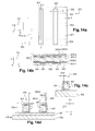
- FIGS. 14 a , 14 b , 14 c and 14 d respectively show a top view and a first, second and third sectional view of a first step of a method according to an embodiment of the invention allowing an integrated circuit to be made with self-aligned contacts using a “gate-first” approach.
- FIGS. 15 a , 15 b , 15 c and 15 d respectively show a top view and a first, second, and third sectional view of a second step in the method according to an embodiment of the invention.
- FIGS. 16 a , 16 b , 16 c and 16 d respectively show a top view and a first, second, and third sectional view of a third step in the method according to an embodiment of the invention.
- FIGS. 17 a , 17 b , 17 c and 17 d respectively show a top view and a first, second, and third sectional view of a fourth step in the method according to an embodiment of the invention.
- FIGS. 18 a , 18 b , 18 c and 18 d respectively show a top view and a first, second, and third sectional view of a fifth step in the method according to an embodiment of the invention.
- FIGS. 19 a , 19 b , 19 c and 19 d respectively show a top view and a first, second, and third sectional view of a sixth step in the method according to an embodiment of the invention.
- FIGS. 20 a , 20 b , 20 c and 20 d respectively show a top view and a first, second, and third sectional view of a seventh step in the method according to an embodiment of the invention.
- FIGS. 21 a , 21 b , 21 c and 21 d respectively show a top view and a first, second, and third sectional view of an eighth step in the method according to an embodiment of the invention.
- FIGS. 22 a , 22 b , 22 c and 22 d respectively show a top view and a first, second, and third sectional view of a ninth step in the method according to an embodiment of the invention.
- FIGS. 23 a , 23 b , 23 c and 23 d respectively show a top view and a first, second, and third sectional view of a tenth step in the method according to an embodiment of the invention.
- FIGS. 24 a , 24 b , 24 c and 24 d respectively show a top view and a first, second, and third sectional view of an eleventh step in the method according to an embodiment of the invention.
- FIGS. 25 a , 25 b , 25 c and 25 d respectively show a top view and a first, second and third sectional view of a twelfth step in the method according to an embodiment of the invention.
- FIGS. 26 a , 26 b , 26 c and 26 d respectively show a top view and a first, second, and third sectional view of a thirteenth step in the method according to an embodiment of the invention.
- FIGS. 27 a , 27 b , 27 c and 27 d respectively show a top view and a first, second, and third sectional view of a fourteenth step in the method according to an embodiment of the invention.
- FIGS. 28 a , 28 b , 28 c and 28 d respectively show a top view and a first, second, and third sectional view of a fifteenth step in the method according to an embodiment of the invention.
- FIG. 29 is a diagram which schematically shows the organisation of the various steps in a method according to an embodiment of the invention.
- FIGS. 14 a to 28 d schematically represent the steps in a method 200 according to an embodiment of the invention in the context of making an integrated circuit with self-aligned contacts and using a “gate-first” approach.
- FIG. 29 is a diagram which summarises the organisation of the various steps in the method 200 according to an embodiment of the invention.
- the method 200 offers an alternative to the conventional approach described previously in association with FIGS. 1 a to 13 , and which is incompatible with the need to preserve the silicide zones on the gate zones.
- a first step 201 in the method 200 is shown in FIGS. 14 a , 14 b , 14 c and 14 d.
- FIG. 14 a shows a top view, along second plane P 2 with orthogonal X and Y axes, of the device during the first step 201 .
- a first section plane A, a second section plane B and a third section plane C are shown in FIG. 14 a .
- the first section plane A and the second section plane B are parallel to the first plane P 1 with orthogonal X and Z axes.
- the third section plane C is parallel to a third section plane P 3 with orthogonal Y and Z axes.
- the third section plane C is therefore perpendicular to the first and to the second section planes A and B.
- FIG. 14 c is a sectional view along the first section plane A of the device during the first step 201 .
- FIG. 14 d is a sectional view along the second section plane B of the device during the first step 201 .
- FIG. 14 b is a sectional view along the third section plane C of the device during the first step 201 .
- the substrate is, in the example shown, an SOI type substrate.
- the substrate may however also be a “bulk” type silicon substrate.
- the substrate is of the SOI type, it comprises an insulating layer 303 , made for example of SiO 2 oxide, also called Box.
- the insulating layer 303 has a thickness measured along the axis OZ which is typically less than 25 nm.
- the initial layer 300 comprises, in the example shown, several active zones 301 , separated from each other by insulation zones 302 .
- the active zones 301 may be made of monocrystalline silicon.
- the insulation zones 302 are formed of a dielectric material, for example an oxide of silicon.
- the active zones 301 and insulation zones 302 extend, in the example shown, over the insulating layer 303 .
- the active zones 301 have a thickness which is typically less than or equal to 5 nm.
- the active zones have 301 have a width W active measured along the Y axis.
- a gate stack 305 is then deposited on the initial layer 300 .
- the gate stack 305 comprises, in the example in this description:
- first layer 305 - 1 is a high-k dielectric layer; embodiments of the invention however are not limited to this and relate more generally to a gate stack 305 which comprises a first layer 305 - 1 of a dielectric.
- a gate stack 305 comprises the second layer 305 - 2 made of titanium nitride; embodiments of the invention however are not restricted to this case and relate more generally to any gate stack comprising the first layer 305 - 1 of a dielectric and the third layer 305 - 3 of a gate conductive layer and which optionally comprises the second layer 305 - 2 .
- the first metal of the fourth layer 305 - 4 is beneficially an alloy of titanium Ti, an alloy of tungsten W, an alloy of tantalum Ta or an alloy of a metal and of silicon Si.
- the fourth layer 305 - 4 can beneficially be obtained by a step of silicidation of the third gate conductive layer 305 - 3 , the gate conductive layer being made, for example, of polycrystalline silicon.
- the second metal of the fifth layer 305 - 5 is beneficially an alloy of titanium Ti, for example titanium nitride, an alloy of tungsten W an alloy of tantalum Ta.
- the height of the gate stack 305 measured along the axis OZ is typically between 30 nm and 75 nm.
- Gate zones 306 are then defined in the gate stack 305 .
- Each gate zone 306 forms a line which extends parallel to the Y axis.
- Each gate zone 306 has, in the example shown, a width of 14 nm, measured along the direction OX.
- the separation spacing step, along direction OX, between the consecutive gate zones 306 also called “pitch” or technology node, is 64 nm in the example shown.
- the dimensions chosen for the gate zones 306 may typically be as follows:
- each gate zone 306 is directly made in the gate stack 305 .
- the gate stack 305 deposited during the first step 201 is directly made up of materials destined to form the gate zones 306 .
- the gate zones 306 may be made in different ways, in particular depending on the desired dimensions of the integrated circuit to be made.
- the gate zones 306 may be made using conventional photo-lithography.
- a mask defining the shape of the gate zones 306 is deposited on the gate stack 305 .
- the gate stack is then illuminated through the mask.
- the illuminated portions of the gate stack 305 are then removed using an appropriate solvent.
- the gate zones 306 can be made using double exposure (“double patterning”) or “spacer patterning” techniques.
- double patterning is known to those skilled in the art and involves carrying out two photo-lithography steps to make a single level.
- a first photo-lithography step is first of all carried out in order to define one of two patterns and then a second photo-lithography step is carried out to define the remaining patterns.
- This technique is used to make patterns with a resolution which can be twice that obtained using conventional lithographic techniques.
- First insulating spacers 307 are then made on either side of each gate zone 306 .
- the first spacers 307 are made of a dielectric material, which may be, for example, a nitride or an oxide/nitride bi-layer. All the first spacers 307 may be made of the same material, or they may be made from different materials.
- the maximum thickness measured along the X axis of the first spacers 307 is typically 8 nm.
- the methods used to make the first insulating spacers 307 are known in the prior art.
- the first insulating spacers 307 can be made, for example, in the following way:
- the upper surfaces of the first insulating spacers 307 can then be planarised such that they are aligned with the upper surfaces of the gate zones 306 . This step may be carried out, for example, by CMP chemical-mechanical polishing.
- the first insulating spacers 307 will contribute to insulating the gate zones 306 from the contacts that will subsequently be made.
- FIGS. 15 a , 15 b , 15 c and 15 d A second step 202 in the method 200 is shown in FIGS. 15 a , 15 b , 15 c and 15 d.
- FIG. 15 a shows a top view along the second plane P 2 of the device during the second step 202 .
- FIG. 15 c is a sectional view along the first section plane A of the device during the second step 202 .
- FIG. 15 d is a sectional view along the second section plane B of the device during the second step 202 .
- FIG. 15 b is a sectional view along the third section plane C of the device during the second step 202 .
- Source and drain zones 308 are made during the second step 202 .
- the zones 308 are located on the active zones 301 on either side of the gate zones 306 on active zones 301 surrounded by the first insulating spacers 307 .
- Making source and drain zones 308 may include a step for epitaxial growth from active zones 301 made of Si.
- Source and drain zones 308 are then beneficially in the form of a truncated a pyramid which has a square base which extends along the second plane P 2 and which typically has a height, measured along axis Z, of 15 nm.
- Each source or drain zone 308 then beneficially has four facets 308 -F which are the four sides of the truncated pyramid.
- the facets 308 -F typically make an angle ⁇ of 72° with the square base. Such facets 308 -F beneficially allow the distances to be increased between, on one hand, the gate zones 306 on active zones 301 and on the other hand source and drain zones 308 adjacent to each gate zone 306 on active zone 301 .
- the source and drain zones 308 are doped in situ if appropriate, during growth, or during a specific implantation step.
- FIGS. 16 a , 16 b , 16 c and 16 d A third step 203 in the method 200 is shown in FIGS. 16 a , 16 b , 16 c and 16 d.
- FIG. 16 a shows a top view along the second plane P 2 of the device during the third step 203 .
- FIG. 16 c is a sectional view along the first section plane A of the device during the third step 203 .
- FIG. 16 d is a sectional view along the second section plane B of the device during the third step 203 .
- FIG. 16 b is a sectional view along the third section plane C of the device during the third step 203 .
- second insulating spacers 309 are made around first insulating spacers 307 .
- the second insulating spacers 309 are made from a dielectric material, for example a nitride.
- the maximum thickness, measured along the X axis, of the second spacers 309 is typically 10 nm.
- the maximum cumulative thickness of the first spacers 307 and of the second spacers 309 measured along the X axis is therefore typically 18 nm.
- a fourth step 204 in the method 200 is shown in FIGS. 17 a , 17 b , 17 c and 17 d.
- FIG. 17 a shows a top view along the second plane P 2 of the device during the fourth step 204 .
- FIG. 17 c is a sectional view along the first section plane A of the device during the fourth step 204 .
- FIG. 17 d is a sectional view along the second section plane B of the device during the fourth step 204 .
- FIG. 17 b is a sectional view along the third section plane C of the device during the fourth step 204 .
- Silicidation zones 310 at the surface of the source and drain zones 308 are made during the fourth step 204 .
- Silicidation is known in the prior art; it is equivalent to the metallisation of source and drain zones 308 using the chemical reaction between the constituent silicon of the source and drain zone 308 and a metal, for example nickel, in order to form zones of low resistivity.
- a metal for example nickel
- no silicidation zone is created at this stage of the method in gate zones 306 , at the surface of which there is still the sixth layer 305 - 6 made of nitride.
- the gate zones 306 already include the fourth layer 305 - 4 of the first metal, which provides a silicidation function.
- a fifth step 205 in the method 200 is shown in FIGS. 18 a , 18 b , 18 c and 18 d.
- FIG. 18 a shows a top view along the second plane P 2 of the device during the fifth step 205 .
- FIG. 18 c is a sectional view along the first section plane A of the device during the fifth step 205 .
- FIG. 18 d is a sectional view along the second section plane B of the device during the fifth step 205 .
- FIG. 18 b is a sectional view along the third section plane C of the device during the fifth step 205 .
- the deposition of a layer 311 of a first level of dielectric, the “inter-layer dielectric” (ILD), is carried out on the device.
- the dielectric material used to form the layer 311 of the ILD first dielectric layer may be, for example, SiO 2 .
- FIGS. 19 a , 19 b , 19 c and 19 d A sixth step 206 in the method 200 is shown in FIGS. 19 a , 19 b , 19 c and 19 d.
- FIG. 19 a shows a top view along the second plane P 2 of the device during the sixth step 206 .
- FIG. 19 c is a sectional view along the first section plane A of the device during the sixth step 206 .
- FIG. 19 d is a sectional view along the second section plane B of the device during the sixth step 206 .
- FIG. 19 b is a sectional view along the third section plane C of the device during the sixth step 206 .
- the layer 311 of the ILD first dielectric layer previously deposited in the fifth step 205 is planarised. This planarisation is, in the example shown, carried out in two steps:
- the space between the first insulating spacers 307 is completely filled by the layer 311 of the first ILD dielectric level.
- a seventh step 207 in the method 200 is shown in FIGS. 20 a , 20 b , 20 c and 20 d.
- FIG. 20 a shows a top view along the second plane P 2 of the device during the seventh step 207 .
- FIG. 20 c is a sectional view along the first section plane A of the device during the seventh step 207 .
- FIG. 20 d is a sectional view along the second section plane B of the device during the seventh step 207 .
- FIG. 20 b is a sectional view along the third section plane C of the device during the seventh step 207 .
- a fourth mask M 4 is made at each insulation zone 302 , in order to protect the insulation zones 302 .
- the distance measured, along the Y axis, between two masks M 4 covering two consecutive insulation zones 302 is greater than the width W active of the active zones 301 .
- the sixth layer 305 - 6 of the dielectric as well as the fifth layer 305 - 5 of the second metal is etched on the active zones 301 not protected by the fourth mask M 4 . Etching is then stopped on the fourth layer 305 - 4 of the first metal.
- the etching on the active zones 301 not protected by the fourth mask M 4 , of the sixth and fifth layers 305 - 6 and 305 - 5 results in a cavity 306 -C appearing at the surface of each gate zone 306 on active zone 301 , between the first insulating spacers 307 .
- the gate zones 306 on insulation zone 302 are protected by the fourth mask M 4 during the seventh step 207 .
- the fourth mask M 4 is then removed.
- the fact that the distance, measured along the Y axis, between two mask M 4 covering two consecutive insulation zones 302 is greater than the width W active of the active zones 301 beneficially means that on the active zones the fifth layer 305 - 5 of the second metal is completely removed and that there is no residue.
- the first metal of the fourth layer 305 - 4 is beneficially an alloy of titanium, an alloy of tungsten, an alloy of tantalum or an alloy of a metal and silicon. More generally any refractory metal is suitable for forming the fourth layer 305 - 4 .
- the second metal of the fifth layer 305 - 5 is beneficially an alloy of titanium, of tungsten or of tantalum. More generally, any refractory material which can be etched selectively, for example by plasma or wet etching, in relation to the first metal, to the layer 311 of the first layer of the ILD dielectric layer and to the materials of the first and second spacers 3074 and 309 , beneficially with a selectivity ratio greater than 5:1 in relation to the first metal, is suitable for forming the fifth layer 305 - 5 .
- refractory metal refers to a metal capable of withstanding a thermal budget of the order of 1000° C., in particular during the creation of the source and drain zones 308 , which usually involves an implantation step followed by a thermal annealing step.
- etching selectivity ratio greater than 5:1 means that during a given etching step, the layer of second metal may be etched more than five times faster than the layer of first metal.
- the first metal is beneficially different from the second metal; that is, the first metal and the second metal beneficially have a different chemical composition, in order to contribute to ensuring that good etching selectivity is achieved. It may be envisaged, however, without going beyond the scope of the invention, that the first metal and the second metal are one and the same material. In this case the fourth layer 305 - 4 and the fifth layer 305 - 5 now only form the same single layer. Stopping the etching of the fifth layer 305 - 5 should then be controlled in order not to consume the fourth layer 305 - 4 .
- FIGS. 21 a , 21 b , 21 c and 21 d An eighth step 208 in the method 200 is shown in FIGS. 21 a , 21 b , 21 c and 21 d.
- FIG. 21 a shows a top view along the second plane P 2 of the device during the eighth step 208 .
- FIG. 21 c is a sectional view along the first section plane A of the device during the eighth step 208 .
- FIG. 21 d is a sectional view along the second section plane B of the device during the eighth step 208 .
- FIG. 21 b is a sectional view along the third section plane C of the device during the eighth step 208 .
- a layer 312 of a dielectric for example a silicon nitride SiN
- the principal role of dielectric material deposited in the layer 312 is to insulate future self-aligned contacts in relation to the gate zones 306 on active zone 301 .
- the dielectric material of layer 312 may in particular be SiN, BN or HfO 2 , deposited using a technique for the deposition of thin atomic layers known as ALD (“Atomic Layer Deposition”) or by a PEALD (“Plasma Enhanced Atomic Layer Deposition”) technique.
- the layer of dielectric 312 is in particular deposited on each gate zone 306 on the active zone 301 , in contact with the fourth layer 305 - 4 of the first metal previously exposed during the seventh step. CMP polishing of the layer 312 of dielectric is then carried out. At the end of this polishing step, the dielectric layer 312 is only preserved over the gate zones 306 on the active zone 301 , thus forming a protective plug over each gate zone 306 on the active zone 301 , which fills the cavities 306 -C formed beforehand.
- These protective plugs contribute to preventing a short-circuit between the gate zones 306 on active zone 301 and source and drain contacts formed later and which are self-aligned with the gate zones 306 on the active zone 301 .
- the protective plugs also contribute to reducing any parasitic capacitive coupling between the gate zones 306 on active zones 301 and the source and drain contacts.
- each gate zone 306 on the active zone 301 thus comprises, in the example shown:
- FIGS. 22 a , 22 b , 22 c and 22 d A ninth step 209 in the method 200 is shown in FIGS. 22 a , 22 b , 22 c and 22 d.
- FIG. 22 a shows a top view along the second plane P 2 of the device during the ninth step 209 .
- FIG. 22 c is a sectional view along the first section plane A of the device during the ninth step 209 .
- FIG. 22 d is a sectional view along the second section plane B of the device during the ninth step 209 .
- FIG. 22 b is a sectional view along the third section plane C of the device during the ninth step 209 .
- a fifth mask M 5 is made at each insulation zone 302 , in order to protect the insulation zones 302 .
- the distance, measured along the Y axis, between two masks M 5 covering two consecutive insulation zones 302 is less than the width W active of the active zones 301 .
- the fifth mask M 5 is a hard mask, for example a hard mask made of nitride.
- the layer 311 of the first ILD dielectric layer present on the active zones 301 and not protected by the fifth mask M 5 is etched. This etching is carried out selectively in relation to the silicidation zones 310 , the first spacers 307 and the second spacers 309 , for example by plasma etching.
- the silicidation zones 310 are exposed.
- the first ILD dielectric level 311 present on the insulation zones 302 is protected by the fifth mask M 5 and it is therefore preserved at the end of the ninth step 209 .
- the fifth mask M 5 is removed.
- FIGS. 23 a , 23 b , 23 c and 23 d A tenth step 210 in the method 200 is shown in FIGS. 23 a , 23 b , 23 c and 23 d.
- FIG. 23 a shows a top view along the second plane P 2 of the device during the tenth step 210 .
- FIG. 23 c is a sectional view along the first section plane A of the device during the tenth step 210 .
- FIG. 23 d is a sectional view along the second section plane B of the device during the tenth step 210 .
- FIG. 23 b is a sectional view along the third section plane C of the device during the tenth step 210 .
- the first constituent material of the source and drain contacts may be any material usually used in the prior art to make source and drain contacts in transistors.
- FIGS. 24 a , 24 b , 24 c and 24 d An eleventh step 211 in the method 200 is shown in FIGS. 24 a , 24 b , 24 c and 24 d.
- FIG. 24 a shows a top view along the second plane P 2 of the device during the eleventh step 211 .
- FIG. 24 c is a sectional view along the first section plane A of the device during the eleventh step 211 .
- FIG. 24 d is a sectional view along the second section plane B of the device during the eleventh step 211 .
- FIG. 24 b is a sectional view along the third section plane C of the device during the eleventh step 211
- CMP polishing of the layer 313 of conductive material previously deposited in the tenth step 210 is carried out in order to break the circuit between the source and drain zones 308 .
- the conductive material is only preserved on the active zones 301 between the gate zones 306 on the active zone 301 . There is no longer any conductive material 313 on the insulation zones 302 .
- the gate zones 306 on the active zones 301 comprise, at the end of the eleventh polishing step 211 :
- Each gate zone 306 on active zone 301 is thus protected by a protective plug 312 which extends over the fourth layer 305 - 4 of the first metal.
- the first metal 305 - 4 which acts as silicide, therefore remains fully present on the active zones 301 , despite the eleventh polishing step 211 .
- the gate zones 306 on the insulation zones 302 comprise, at the end of the eleventh polishing step 211 :
- a twelfth step 212 in the method 200 is shown in FIGS. 25 a , 25 b , 25 c and 25 d.
- FIG. 25 a shows a top view along the second plane P 2 of the device during the twelfth step 212 .
- FIG. 25 c is a sectional view along the first section plane A of the device during the twelfth step 212 .
- FIG. 25 d is a sectional view along the second section plane B of the device during the twelfth step 212 .
- FIG. 25 b is a sectional view along the third section plane C of the device during the twelfth step 212 .
- the gate zones 306 on active zone 301 are protected during the twelfth step 212 by the nitride plugs 312 .
- FIGS. 26 a , 26 b , 26 c and 26 d A thirteenth step 213 in the method 200 is shown in FIGS. 26 a , 26 b , 26 c and 26 d.
- FIG. 26 a shows a top view along the second plane P 2 of the device during the thirteenth step 213 .
- FIG. 26 c is a sectional view along the first section plane A of the device during the thirteenth step 213 .
- FIG. 26 d is a sectional view along the second section plane B of the device during the thirteenth step 213 .
- FIG. 26 b is a sectional view along the third section plane C of the device during the thirteenth step 213 .
- an etch stop layer (ESL) 314 is carried out.
- the layer 314 is, for example, a silicon nitride.
- a polishing step of the etch stop layer (ESL) 314 may be carried out, for example using a chemical-mechanical polishing step (CMP).
- FIGS. 27 a , 27 b , 27 c and 27 d A fourteenth step 214 in the method 200 is shown in FIGS. 27 a , 27 b , 27 c and 27 d.
- FIG. 27 a shows a top view along the second plane P 2 of the device during the fourteenth step 214 .
- FIG. 27 c is a sectional view along the first section plane A of the device during the fourteenth step 214 .
- FIG. 27 d is a sectional view along the second section plane B of the device during the fourteenth step 214 .
- FIG. 27 b is a sectional view along the third section plane C of the device during the fourteenth step 214 .
- the fourteenth step 214 the deposition of a layer 315 of a second level of ILD dielectric 315 is carried out.
- FIGS. 28 a , 28 b , 28 c and 28 d A fifteenth step 215 in the method 200 is shown in FIGS. 28 a , 28 b , 28 c and 28 d.
- FIG. 28 a shows a top view along the second plane P 2 of the device during the fifteenth step 215 .
- FIG. 28 c is a sectional view along the first section plane A of the device during the fifteenth step 215 .
- FIG. 28 d is a sectional view along the second section plane B of the device during the fifteenth step 215 .
- FIG. 28 b is a sectional view along the third section plane C of the device during the fifteenth step 215 .
- a start is made by defining the contours of future source, drain and gate contacts, that is, the patterning of the contacts is carried out using lithography.
- Source and drain contacts 317 are to be located on active zone 301 on either side of the gate zones 306 on active zone 301 .
- a gate contact 318 will be located on the insulation zone 302 .
- the levels of source and drain contact 317 and gate contacts 318 are then opened by an etching step on the layer 315 of the second ILD dielectric level and of the ESL stop layer 314 . Then the deposition of a conductive material 316 in the previously defined contact levels is carried out.
- the method of an embodiment of the invention beneficially contributes towards a particular profile being obtained which allows the creation of a gate contact 308 function on insulation zone 302 and of gate zones 306 on active zones 301 .
- the fourth layer 305 - 4 of the gates zones 306 on active zones 301 has a coordinate Z 1 along the Z axis.
- the lower level of the gate contacts 318 and source and drain contacts 317 have a coordinate Z 2 along the Z axis.
- the method 200 beneficially allows gate zones 306 to be made on active zones 310 whose fourth layer 305 - 4 of first metal, which is substantially parallel to the plane P 2 , is located below the lower level, also substantially parallel to the plane P 2 , the gate contacts 318 and source and drain contacts 317 ; that is to say Z 1 is lower than Z 2 .
Landscapes
- Engineering & Computer Science (AREA)
- Manufacturing & Machinery (AREA)
- Microelectronics & Electronic Packaging (AREA)
- Power Engineering (AREA)
- Computer Hardware Design (AREA)
- General Physics & Mathematics (AREA)
- Physics & Mathematics (AREA)
- Condensed Matter Physics & Semiconductors (AREA)
- Electrodes Of Semiconductors (AREA)
- Insulated Gate Type Field-Effect Transistor (AREA)
- Chemical & Material Sciences (AREA)
- Composite Materials (AREA)
- Materials Engineering (AREA)
- Metal-Oxide And Bipolar Metal-Oxide Semiconductor Integrated Circuits (AREA)
- Chemical Kinetics & Catalysis (AREA)
Abstract
Description
-
- a first layer 15-1 of a high-k dielectric, with the first layer 15-1 extending over the
substrate 10; - a second layer 15-2 of titanium nitride, with the second layer 15-2 extending over the first layer 15-1;
- a third layer 15-3 of polysilicon, with the third layer 15-3 extending over the second layer 15-2;
- a fourth layer 15-4 of a dielectric, for example a nitride, with the fourth layer 15-4 extending over the third layer 15-3;
- a first layer 15-1 of a high-k dielectric, with the first layer 15-1 extending over the
-
- making a gate stack on the surface of an active zone, comprising the following steps:
- deposition of a first gate dielectric layer which extends over the active zone;
- deposition of a gate conductive layer which extends over the layer of first dielectric;
- deposition of a layer of a first metal, where the layer of the first metal extends over the gate conductive layer;
- deposition of a layer of a second metal, where the layer of the second metal extends over the layer of the first metal;
- deposition of a layer of a second dielectric extending over the layer of the second metal;
- partial etching of the gate stack for the formation of a gate zone on the active zone;
- making insulating spacers on either side of the gate zone on the active zone;
- making source and drain electrodes zones;
- making silicidation zones on the surface of the source and drain zones; etching, in the gate zone on the active zone, of the second dielectric layer and of the layer of second metal with a stop on the layer of the first metal, so as to form a cavity between the insulating spacers;
- making a protective plug at the surface of the layer of first metal of the gate zone on the active zone, where the protective plug fills the cavity.
- making a gate stack on the surface of an active zone, comprising the following steps:
-
- The layer of first metal is a layer made of a refractory metal alloy. A refractory metal is a metal capable of withstanding a thermal budget of the order of 1000° C., in particular during the creation of the source and drain zones, which usually involves an implantation step followed by a thermal annealing step.
- The layer of first metal is a layer made of one of the following materials
- an alloy of Titanium Ti;
- an alloy of Tungsten W;
- an alloy of Tantalum Ta;
- an alloy of a metal and silicon Si;
- When the layer of the first metal is an alloy of metal and silicon, the layer of first metal can beneficially be obtained by a step of silicidation of the gate conductive layer, the gate conductive layer then being made, for example, of polycrystalline silicon.
- The layer of the second metal is a layer made of a refractory metal alloy.
- The layer of the second metal is a layer made of one of the following materials
- an alloy of Titanium Ti;
- an alloy of Tungsten W;
- an alloy of Tantalum Ta;
- an alloy of any other refractory metal.
- The first metal of the layer of first metal layer is beneficially different from the second metal of the layer of the second metal. Thus during etching of the dielectric layer and of the layer of second metal, stopping the etching on the layer of first metal in order to preserve the layer of first metal is facilitated,
- The layer of second metal may be etched selectively relative to the layer of the first metal.
- The selectivity ratio between etching of the layer of second metal and etching of the layer of first metal is greater than 5:1.
- The term “selectivity ratio between etching of the layer of second metal and etching of the layer of first metal is greater than 5:1” means that during a given etching step, the layer of second metal may be etched five times faster than the layer of first metal,
- The thickness of the layer of first metal is greater than or equal to 15 nm.
- The layer of second metal has a thickness between 20 nm and 50 nm.
- The thickness of the gate conductive layer is greater than or equal to 15 nm.
- The cumulative thickness of the gate conductive layer and of the layer of first metal is less than or equal to 100 nm.
- The method of an embodiment of the invention moreover comprises the following steps:
- deposition of a conductive layer over the entire device;
- polishing of the conductive layer in order to break the circuit between the source and drain silicidation zones.
- The method of an embodiment of the invention moreover comprises the following steps:
- deposition of a stop layer over the entire device;
- deposition of a layer of a dielectric on the stop layer;
- selective etching of the dielectric layer and of the stop layer to expose the conductive layer, so as to cut trenches above the source and drain silicidation zones;
- filling of the trenches with a conductive material in order to make contacts on the source and drain silicidation zones.
- Integrated circuit obtained by a manufacturing method according to an embodiment of the invention, comprising:
- at least one active zone and at least one insulation zone;
- at least one gate zone on the active zone, comprising a layer of first dielectric, a gate conductive layer, a layer of a first metal and a protective plug;
- at least one gate zone on the insulation zone, comprising a layer of first dielectric, a gate conductive layer, a layer of a first metal and a layer of a second metal.
-
- a first layer 305-1 of a high-k dielectric, with the first layer 305-1 extending over the
initial layer 300; - a second layer 305-2 of titanium nitride, with the second layer 305-2 extending over the first layer 305-1;
- a third layer 305-3 of a gate conductive material, for example polysilicon, with the third layer 305-3 extending over the second layer 305-2;
- a fourth layer 305-4 of a first metal, with the fourth layer 305-4 extending over the third layer 305-3;
- a fifth layer 305-5 of a second metal, with the fifth layer 305-5 extending over the fourth layer 305-4;
- a sixth layer 305-6 of a dielectric, for example a nitride, with the sixth layer 305-6 extending over the fifth layer 305-5;
- a first layer 305-1 of a high-k dielectric, with the first layer 305-1 extending over the
-
- The first layer 305-1 of dielectric typically has a thickness, measured along axis OZ, of 5 nm;
- The second layer 305-2 typically has a thickness, measured along axis OZ, of 5 nm;
- the third layer 305-3 and the fourth layer 305-4 respectively have a thickness, measured along the Z axis, typically greater than or equal to 15 nm, with the sum of the thickness of the third layer 305-3 and of the thickness of the fourth layer 305-4 being between 30 nm and 100 nm. The smaller the desired technology node, then beneficially, the smaller the sum of the thicknesses of the third layer 305-3 and of the fourth layer 305-4, so as to minimise any parasitic capacitances. The thickness of the fourth layer 305-4 should, however, be sufficient to reduce the resistivity of the
gate zone 306; - the thickness of the fifth layer 305-5 of second metal is typically, measured along the OZ axis, between 20 nm and 50 nm. The thickness of the fifth layer 305-5 is chosen in accordance with the need to perform the later polishing and etching steps, and in particular in accordance with the need for selectivity of etching and/or for precision of the etching stop that has to be implemented. In effect, one wishes to ensure that the thickness of the layer 305-5 will be sufficient for the fourth layer 305-4 to be preserved at the surface of the
gate zones 306; - the sixth layer 305-6 of dielectric typically has a thickness, measured along axis OZ, of 15 nm;
-
- a layer of insulating material forming the first insulating spacers 307 (for example nitride or a nitride-oxide bi-layer) is deposited over all the
gate zones 306 and over theinitial layer 300; - the layer of insulating material is anisotropically etched so as to preserve the vertical parts of the layer made of insulating material. The vertical parts of the layer made of insulating material then form the
first spacers 307 on either side of eachgate zone 306.
- a layer of insulating material forming the first insulating spacers 307 (for example nitride or a nitride-oxide bi-layer) is deposited over all the
-
- firstly a partial CMP chemical-mechanical polishing is carried out, at the end of which a portion of the thickness of the
layer 311 of the first ILD dielectric level, measured along the Z axis, remains at the surface of thegate zones 306. The CMP chemical-mechanical polishing is therefore stopped a little before the upper surface of thegate zones 306; - then a finishing polishing step is carried out using an etch-back method which ends up at the surface of the
gate zones 306 in order to expose the sixth layer 305-6.
- firstly a partial CMP chemical-mechanical polishing is carried out, at the end of which a portion of the thickness of the
-
- the first layer of dielectric 305-1;
- the second layer of titanium nitride 305-2;
- the third gate conductive layer 305-3;
- the fourth layer 305-4 of first metal;
- the
protective plug 312 made of dielectric material.
-
- the first layer 305-1 of a high-k dielectric, which extends over the
initial layer 300; - the second layer 305-2 of titanium nitride, which extends over the first layer 305-1;
- the third layer 305-3 of polysilicon, which extends over the second layer 305-2;
- the fourth layer 305-4 of the first metal which extends over the third layer 305-3;
- the
protective plug 312 made of dielectric material.
- the first layer 305-1 of a high-k dielectric, which extends over the
-
- the first layer 305-1 of a high-k dielectric, which extends over the
initial layer 300; - the second layer 305-2 of titanium nitride, which extends over the first layer 305-1;
- the third layer 305-3 of polysilicon, which extends over the second layer 305-2;
- the fourth layer 305-4 of the first metal which extends over the third layer 305-3;
- the fifth layer 305-5 of the second metal which extends over the fourth layer 305-4;
- the sixth layer 305-6 of dielectric, which extends over the fifth layer 305-5;
- the first layer 305-1 of a high-k dielectric, which extends over the
-
- the sixth layer 305-6 of dielectric, which remained only on the
insulation zones 302 at the end of theseventh step 207; - the fifth layer 305-5 of the second metal which also remained on the
insulation zones 302.
- the sixth layer 305-6 of dielectric, which remained only on the
Claims (15)
Priority Applications (1)
| Application Number | Priority Date | Filing Date | Title |
|---|---|---|---|
| US14/965,519 US20160099326A1 (en) | 2013-09-27 | 2015-12-10 | Method for making an integrated circuit |
Applications Claiming Priority (2)
| Application Number | Priority Date | Filing Date | Title |
|---|---|---|---|
| FR1359365A FR3011382B1 (en) | 2013-09-27 | 2013-09-27 | METHOD FOR PRODUCING AN INTEGRATED CIRCUIT |
| FR1359365 | 2013-09-27 |
Related Child Applications (1)
| Application Number | Title | Priority Date | Filing Date |
|---|---|---|---|
| US14/965,519 Division US20160099326A1 (en) | 2013-09-27 | 2015-12-10 | Method for making an integrated circuit |
Publications (2)
| Publication Number | Publication Date |
|---|---|
| US20150091106A1 US20150091106A1 (en) | 2015-04-02 |
| US9240325B2 true US9240325B2 (en) | 2016-01-19 |
Family
ID=49753384
Family Applications (2)
| Application Number | Title | Priority Date | Filing Date |
|---|---|---|---|
| US14/498,091 Active US9240325B2 (en) | 2013-09-27 | 2014-09-26 | Method for making an integrated circuit |
| US14/965,519 Abandoned US20160099326A1 (en) | 2013-09-27 | 2015-12-10 | Method for making an integrated circuit |
Family Applications After (1)
| Application Number | Title | Priority Date | Filing Date |
|---|---|---|---|
| US14/965,519 Abandoned US20160099326A1 (en) | 2013-09-27 | 2015-12-10 | Method for making an integrated circuit |
Country Status (2)
| Country | Link |
|---|---|
| US (2) | US9240325B2 (en) |
| FR (1) | FR3011382B1 (en) |
Families Citing this family (1)
| Publication number | Priority date | Publication date | Assignee | Title |
|---|---|---|---|---|
| US11929314B2 (en) * | 2021-03-12 | 2024-03-12 | Taiwan Semiconductor Manufacturing Company, Ltd. | Interconnect structures including a fin structure and a metal cap |
Citations (8)
| Publication number | Priority date | Publication date | Assignee | Title |
|---|---|---|---|---|
| US5686329A (en) | 1995-12-29 | 1997-11-11 | Taiwan Semiconductor Manufacturing Company, Ltd. | Method for forming a metal oxide semiconductor field effect transistor (MOSFET) having improved hot carrier immunity |
| US20050095797A1 (en) | 2003-10-29 | 2005-05-05 | Hynix Semiconductor Inc. | Method for fabricating semiconductor device with use of partial gate recessing process |
| US20050095793A1 (en) * | 2003-10-31 | 2005-05-05 | Hynix Semiconductor Inc. | Transistor of semiconductor device and method for manufacturing the same |
| US20070026578A1 (en) | 2005-07-28 | 2007-02-01 | Hyun-Su Kim | Method for forming a silicided gate |
| US20070296052A1 (en) * | 2006-06-26 | 2007-12-27 | Taiwan Semiconductor Manufacturing Company, Ltd. | Methods of forming silicide regions and resulting MOS devices |
| US20080224325A1 (en) * | 2007-03-16 | 2008-09-18 | Fujitsu Limited | Wiring board, mounting structure for electronic components, and semiconductor device |
| US20080224235A1 (en) | 2007-03-15 | 2008-09-18 | Lavoie Adrien R | Selectively depositing aluminium in a replacement metal gate process |
| WO2011090571A2 (en) | 2009-12-30 | 2011-07-28 | Intel Corporation | Self-aligned contacts |
Family Cites Families (15)
| Publication number | Priority date | Publication date | Assignee | Title |
|---|---|---|---|---|
| US6764911B2 (en) * | 2002-05-10 | 2004-07-20 | Taiwan Semiconductor Manufacturing Co., Ltd | Multiple etch method for fabricating spacer layers |
| US7019351B2 (en) * | 2003-03-12 | 2006-03-28 | Micron Technology, Inc. | Transistor devices, and methods of forming transistor devices and circuit devices |
| KR100502426B1 (en) * | 2003-09-18 | 2005-07-20 | 삼성전자주식회사 | Semiconductor devices having dual gates and methods of forming the same |
| JP4904815B2 (en) * | 2003-10-09 | 2012-03-28 | 日本電気株式会社 | Semiconductor device and manufacturing method thereof |
| KR100560818B1 (en) * | 2004-06-02 | 2006-03-13 | 삼성전자주식회사 | Semiconductor device and manufacturing method thereof |
| US7598545B2 (en) * | 2005-04-21 | 2009-10-06 | International Business Machines Corporation | Using metal/metal nitride bilayers as gate electrodes in self-aligned aggressively scaled CMOS devices |
| JP4718908B2 (en) * | 2005-06-14 | 2011-07-06 | 株式会社東芝 | Semiconductor device and manufacturing method of semiconductor device |
| JP2007005721A (en) * | 2005-06-27 | 2007-01-11 | Toshiba Corp | Semiconductor device and manufacturing method thereof |
| JP4940682B2 (en) * | 2005-09-09 | 2012-05-30 | 富士通セミコンダクター株式会社 | Field effect transistor and manufacturing method thereof |
| JP2008103644A (en) * | 2006-10-20 | 2008-05-01 | Toshiba Corp | Semiconductor device and manufacturing method thereof |
| FR2930073B1 (en) * | 2008-04-11 | 2010-09-03 | Centre Nat Rech Scient | METHOD FOR MANUFACTURING COMPLEMENTARY P AND N TYPE MOSFET TRANSISTORS, AND ELECTRONIC DEVICE COMPRISING SUCH TRANSISTORS, AND PROCESSOR COMPRISING AT LEAST ONE SUCH DEVICE. |
| US20130032886A1 (en) * | 2011-08-01 | 2013-02-07 | International Business Machines Corporation | Low Threshold Voltage And Inversion Oxide Thickness Scaling For A High-K Metal Gate P-Type MOSFET |
| KR20110137435A (en) * | 2010-06-17 | 2011-12-23 | 삼성전자주식회사 | Manufacturing Method of Semiconductor Device |
| WO2012107970A1 (en) * | 2011-02-10 | 2012-08-16 | パナソニック株式会社 | Semiconductor device |
| WO2013101007A1 (en) * | 2011-12-28 | 2013-07-04 | Intel Corporation | Methods of integrating multiple gate dielectric transistors on a tri-gate (finfet) process |
-
2013
- 2013-09-27 FR FR1359365A patent/FR3011382B1/en active Active
-
2014
- 2014-09-26 US US14/498,091 patent/US9240325B2/en active Active
-
2015
- 2015-12-10 US US14/965,519 patent/US20160099326A1/en not_active Abandoned
Patent Citations (8)
| Publication number | Priority date | Publication date | Assignee | Title |
|---|---|---|---|---|
| US5686329A (en) | 1995-12-29 | 1997-11-11 | Taiwan Semiconductor Manufacturing Company, Ltd. | Method for forming a metal oxide semiconductor field effect transistor (MOSFET) having improved hot carrier immunity |
| US20050095797A1 (en) | 2003-10-29 | 2005-05-05 | Hynix Semiconductor Inc. | Method for fabricating semiconductor device with use of partial gate recessing process |
| US20050095793A1 (en) * | 2003-10-31 | 2005-05-05 | Hynix Semiconductor Inc. | Transistor of semiconductor device and method for manufacturing the same |
| US20070026578A1 (en) | 2005-07-28 | 2007-02-01 | Hyun-Su Kim | Method for forming a silicided gate |
| US20070296052A1 (en) * | 2006-06-26 | 2007-12-27 | Taiwan Semiconductor Manufacturing Company, Ltd. | Methods of forming silicide regions and resulting MOS devices |
| US20080224235A1 (en) | 2007-03-15 | 2008-09-18 | Lavoie Adrien R | Selectively depositing aluminium in a replacement metal gate process |
| US20080224325A1 (en) * | 2007-03-16 | 2008-09-18 | Fujitsu Limited | Wiring board, mounting structure for electronic components, and semiconductor device |
| WO2011090571A2 (en) | 2009-12-30 | 2011-07-28 | Intel Corporation | Self-aligned contacts |
Non-Patent Citations (2)
| Title |
|---|
| E.P. Gusev et al., "Advanced high-k dielectric stacks with polySi and metal gates: Recent progress and current challenges", IBM Journal of Research and Development, Jul./Sep. 2006, pp. 387-410, XP55106143. |
| Search Report and Written Opinion issued for French Patent Application No. 1359365, dated Mar. 13, 2014. |
Also Published As
| Publication number | Publication date |
|---|---|
| US20150091106A1 (en) | 2015-04-02 |
| US20160099326A1 (en) | 2016-04-07 |
| FR3011382A1 (en) | 2015-04-03 |
| FR3011382B1 (en) | 2019-03-29 |
Similar Documents
| Publication | Publication Date | Title |
|---|---|---|
| US11948839B2 (en) | Power reduction in finFET structures | |
| KR101879051B1 (en) | Semiconductor device and manufacturing method thereof | |
| KR102123920B1 (en) | Semiconductor device and method of manufacture | |
| US9882029B2 (en) | Semiconductor device including Fin-FET and manufacturing method thereof | |
| US9947766B2 (en) | Semiconductor device and fabricating method thereof | |
| US9147765B2 (en) | FinFET semiconductor devices with improved source/drain resistance and methods of making same | |
| KR101363699B1 (en) | Metal gate semiconductor device | |
| KR101976916B1 (en) | Semiconductor device and method | |
| US10325848B2 (en) | Self-aligned local interconnect technology | |
| KR20190002301A (en) | Metal gate structure cutting process | |
| KR20180120637A (en) | Semiconductor device and manufacturing method thereof | |
| US9680017B2 (en) | Semiconductor device including Fin FET and manufacturing method thereof | |
| KR101954509B1 (en) | Semiconductor device and method | |
| KR20180078126A (en) | A semiconductor device and a method for fabricating the same | |
| US10276574B2 (en) | Semiconductor device and manufacturing method thereof | |
| CN103489784B (en) | There is semiconductor device and the manufacture method thereof of the gate height uniformity of improvement | |
| CN108074817A (en) | Method for forming semiconductor device | |
| US11676869B2 (en) | Semiconductor device and manufacturing method thereof | |
| CN108878529B (en) | Semiconductor device and method for manufacturing the same | |
| KR102370296B1 (en) | Semiconductor device and method of manufacture | |
| US11404418B2 (en) | Semiconductor device and manufacturing method thereof | |
| CN102299092B (en) | Semiconductor device and forming method thereof | |
| US9240325B2 (en) | Method for making an integrated circuit | |
| CN115458601A (en) | Semiconductor device and method for manufacturing the same |
Legal Events
| Date | Code | Title | Description |
|---|---|---|---|
| AS | Assignment |
Owner name: COMMISSARIAT A L'ENERGIE ATOMIQUE ET AUX ENERGIES Free format text: ASSIGNMENT OF ASSIGNORS INTEREST;ASSIGNOR:BARNOLA, SEBASTIEN;REEL/FRAME:035231/0789 Effective date: 20150319 Owner name: STMICROELECTRONICS (CROLLES 2) SAS, FRANCE Free format text: ASSIGNMENT OF ASSIGNORS INTEREST;ASSIGNORS:MORAND, YVES;NIEBOJEWSKI, HEIMANU;REEL/FRAME:035231/0685 Effective date: 20150319 Owner name: STMICROELECTRONICS SA, FRANCE Free format text: ASSIGNMENT OF ASSIGNORS INTEREST;ASSIGNORS:MORAND, YVES;NIEBOJEWSKI, HEIMANU;REEL/FRAME:035231/0685 Effective date: 20150319 |
|
| STCF | Information on status: patent grant |
Free format text: PATENTED CASE |
|
| MAFP | Maintenance fee payment |
Free format text: PAYMENT OF MAINTENANCE FEE, 4TH YEAR, LARGE ENTITY (ORIGINAL EVENT CODE: M1551); ENTITY STATUS OF PATENT OWNER: LARGE ENTITY Year of fee payment: 4 |
|
| MAFP | Maintenance fee payment |
Free format text: PAYMENT OF MAINTENANCE FEE, 8TH YEAR, LARGE ENTITY (ORIGINAL EVENT CODE: M1552); ENTITY STATUS OF PATENT OWNER: LARGE ENTITY Year of fee payment: 8 |
|
| AS | Assignment |
Owner name: STMICROELECTRONICS FRANCE, FRANCE Free format text: CHANGE OF NAME;ASSIGNOR:STMICROELECTRONICS SA;REEL/FRAME:066124/0686 Effective date: 20230126 |