US9223541B2 - Method and apparatus to eliminate frequency holes in a memory I/O system - Google Patents
Method and apparatus to eliminate frequency holes in a memory I/O system Download PDFInfo
- Publication number
- US9223541B2 US9223541B2 US13/682,487 US201213682487A US9223541B2 US 9223541 B2 US9223541 B2 US 9223541B2 US 201213682487 A US201213682487 A US 201213682487A US 9223541 B2 US9223541 B2 US 9223541B2
- Authority
- US
- United States
- Prior art keywords
- signal path
- processor
- skew
- memory device
- data signal
- Prior art date
- Legal status (The legal status is an assumption and is not a legal conclusion. Google has not performed a legal analysis and makes no representation as to the accuracy of the status listed.)
- Active, expires
Links
Images


Classifications
-
- G—PHYSICS
- G06—COMPUTING; CALCULATING OR COUNTING
- G06F—ELECTRIC DIGITAL DATA PROCESSING
- G06F5/00—Methods or arrangements for data conversion without changing the order or content of the data handled
- G06F5/06—Methods or arrangements for data conversion without changing the order or content of the data handled for changing the speed of data flow, i.e. speed regularising or timing, e.g. delay lines, FIFO buffers; over- or underrun control therefor
- G06F5/065—Partitioned buffers, e.g. allowing multiple independent queues, bidirectional FIFO's
-
- G—PHYSICS
- G06—COMPUTING; CALCULATING OR COUNTING
- G06F—ELECTRIC DIGITAL DATA PROCESSING
- G06F1/00—Details not covered by groups G06F3/00 - G06F13/00 and G06F21/00
- G06F1/04—Generating or distributing clock signals or signals derived directly therefrom
- G06F1/10—Distribution of clock signals, e.g. skew
-
- G—PHYSICS
- G06—COMPUTING; CALCULATING OR COUNTING
- G06F—ELECTRIC DIGITAL DATA PROCESSING
- G06F2205/00—Indexing scheme relating to group G06F5/00; Methods or arrangements for data conversion without changing the order or content of the data handled
- G06F2205/06—Indexing scheme relating to groups G06F5/06 - G06F5/16
- G06F2205/067—Bidirectional FIFO, i.e. system allowing data transfer in two directions
Definitions
- This invention relates generally to computing devices utilizing memory devices and to methods and apparatus for managing signals between memory devices and other devices.
- DRAM dynamic random access memory
- a processor may include logic that provides synchronous clocking for the data bus channel and the clock channel
- some conventional DRAMS tend to introduce skew between the signals received from a processor on the data bus channel and the clock channel. The skew is seldom constant, but instead exhibits phase jitter and/or drift over time and as a function of temperature.
- phase jitter If the amount of phase jitter exceeds certain thresholds for a given system, the signal received at the memory device will be flagged as an error, resulting in a so-called “memory operating frequency hole.” Memory operating frequency holes can lead to lower device performance or other errors.
- phase jitter One conventional technique to address the issue of phase jitter is to impose sufficient wide band isolation, through silicon design, package design or both, between the processor and the memory device input/outputs (I/Os). This technique tends to be costly. Other conventional techniques involve over or under clocking the processor and/or the memory, which may not be practical for various reasons.
- the present invention is directed to overcoming or reducing the effects of one or more of the foregoing disadvantages.
- a method of managing signals between a processor and a memory device wherein the processor and the memory device are operatively coupled by a data signal path and a clock signal path is provided.
- the method includes setting the skew between the data signal path and the clock signal path away from a spectral peak of a phase jitter transfer function.
- a method of managing signals between a processor and a memory device of a computing device wherein the processor and the memory device are operatively coupled by a data signal path, a clock signal path and an error detection signal path is provided.
- the method includes setting the skew between the data signal path and the clock signal path away from a spectral peak of a phase jitter transfer function.
- an apparatus in accordance with another aspect of an embodiment of the present invention, includes a processor and a memory device operatively coupled to the processor by a data signal path and a clock signal path.
- the processor is operable to set the skew between the data signal path and the clock signal path away from a spectral peak of a phase jitter transfer function.
- FIGS. 1A and 1B are a block diagram of an exemplary embodiment of a computing device that includes a processor and a memory device;
- FIG. 2 is a system model diagram for an exemplary physical layer portion of the processor and the memory device
- FIG. 3 is a graph of an exemplary transfer function representing phase jitter between clock and data signal paths of the processor and the memory device;
- FIG. 4 is a graph of an exemplary performance phase jitter optimization algorithm curve
- FIG. 5 is a simplified depiction of the exemplary system model diagram of FIG. 2 .
- An exemplary method includes setting the skew between the data signal path and the clock signal path away from a spectral peak, and possibly to at least one spectral null, of a phase jitter transfer function. When set to the spectral null, the transmit noise due to phase jitter is attenuated. Additional details will now be described.
- FIG. 1 FIGS. 1A and 1B therein is depicted a block diagram of an exemplary embodiment of a computing device 10 that includes a processor 15 and a memory device 20 .
- the computing device 10 may be a computer, a digital television, a handheld mobile device, a personal computer, a server, a memory device, an add-in board such as a graphics card, or any other computing device employing semiconductors.
- the processor 15 may be a microprocessor, a graphics processor, a combined microprocessor/graphic processor, an application specific integrated circuit, a communications device or other.
- the memory device 20 may be a random access memory or other type of memory device.
- the processor 15 is linked electrically or optically to the memory device 20 by a data bus channel 25 , a clock channel 30 and an error detection channel 35 .
- the data bus channel 25 and the clock channel 30 are operable to deliver data and clock signals from the processor 15 to the memory device 20 and the error detection channel 35 is operable to deliver error detection signals from the memory device 20 to the processor 15 .
- the processor 15 is a graphics processor that includes processor engines 40 and a memory controller 45 .
- the processor engines 40 and the memory controller 45 are linked by a multi-channel bus 50 .
- a system level clocking function is provided by an oscillator 55 and a system phase lock loop (PLL) 60 .
- the oscillator 55 is operable to deliver some oscillating signal with a frequency F REF-SYS .
- the processor 15 includes a physical device layer (PHY) 65 .
- the PHY 65 includes a FIFO read and write block 70 associated with the data bus channel 25 and FIFO read and write block 75 associated with the clock channel 30 .
- the FIFO read/write block 70 is linked to the memory controller 45 by a bus 80 and the FIFO read and write block 75 is linked to the memory controller 45 by way of another bus 85 .
- the output 90 of the FIFO read and write block 70 is tied to a serializer 95 .
- the serializer 95 is, in-turn, linked to a transmitter 100 associated with the data bus channel 25 .
- the FIFO read and write block 75 similarly has an output 105 that is tied to another serializer 110 that, in-turn, feeds a transmitter 115 associated with the clock channel 30 .
- the PHY layer 65 includes an I/O PLL 120 that is fed by an oscillator 125 supplying some frequency F REF — I/O .
- the output 130 of the I/O PLL 120 is fed to the transmitters 100 and 115 .
- delay elements 140 and 145 associated with the pathways to the transmitters 100 and 115 respectively.
- the delay element 140 has some delay value ⁇ T d0 and the delay element 145 has some delay value ⁇ T c0 .
- the values of ⁇ T d0 and ⁇ T c0 may be modified selectively in order to correlate the phase noise associated with the data bus channel 25 and the clock channel 30 .
- the delay elements 140 and 145 may be implemented in a variety ways, such integrated circuits, a combination of plural inverters and a multiplexer or other circuitry that provides selectable time delay.
- the error detection channel 35 is connected to a receiver deserializer 150 that provides an input 155 to clock recovery logic 160 and another input to a signature analyzer error detection control loop 165 .
- the error detection control loop 165 provides output signals at 170 and 175 that can modify the values ⁇ T d0 and ⁇ T d0 to be described in more detail below.
- the error detection control loop 165 is tied electrically to the memory controller 45 by way of a bus 180 .
- the data bus channel 25 is connected to a receiver 185 in the memory device 20 .
- the output 195 of the receiver is tied to a deserializer 200 .
- the output 205 of the deserializer 200 is delivered to TO FIFO logic of the memory device 20 .
- the deserializer provides output data on a data bus 210 that is used by a received data signature generator 215 , which is designed to facilitate send and received data comparison for error detection purposes.
- the output 220 of the received data signature generator 215 is tied to a serializer 225 .
- the output of the serializer 230 is tied to a transmitter 235 that is connected to the error detection channel 35 .
- the clock channel 30 is connected to a PLL filter 240 and in parallel to a multiplexer 245 .
- the output of the PLL filter 240 is similarly tied to the multiplexer 245 .
- the output of the multiplexer 245 has associated with it respective delay elements 250 and 255 that have respective delay values ⁇ T c1 and ⁇ T c2 .
- These delay values ⁇ T c1 and ⁇ T c2 are configurable by way of registers 260 and 265 . In this way, clock signals from the clock channel 30 may be delivered to the receiver 185 and the transmitter 235 with some selected delays ⁇ T c1 and ⁇ T c2 .
- FIG. 2 A system model diagram for the physical layer 65 and the memory device 20 is depicted in FIG. 2 .
- the block H PHY-PLL(f) corresponds to the I/O PLL 120 shown in FIG. 1A .
- the output of the I/O PLL 120 (also shown in FIG. 1A ) and designated as block H PHY-PLL(f) in FIG. 2 is a signal X 0 .
- there is a phase shift associated with the delay element 135 that has a value e ⁇ i ⁇ f ⁇ Tc .
- noise signal N engine(f) that is associated with the processor engines 40 depicted in FIG. 1A and there is a noise component N PHY(f) associated with the physical device layer 65 itself shown in FIG. 1A .
- the signal X 1 is the combination of the X 0 signal and the noise components N PHY-PLL(f) , N engine(f) and N PHY(f) and the phase shift e ⁇ i2 ⁇ f ⁇ Tc delivered commonly to the delay elements 140 and 145 at node x 1 .
- the phase shift associated with the delay element 140 shown in FIG. 1A and thus the transmitter 100 is given by e ⁇ i2 ⁇ Td0 and the phase shift associated with the delay element 145 and thus the transmitter 115 shown at FIG.
- Node x 2 has a crosstalk noise input N xtlk-clock(f) resulting in output at node x 4 and node x 3 has a crosstalk noise input N xtlk-data(f) resulting in output at node x 5 .
- these crosstalk inputs N xtlk-clock(f) and N xtlk-data(f) will be ignored for computational purposes.
- the combined X 1 and e ⁇ i2 ⁇ f ⁇ Tc0 signal is delivered to the PLL filter 240 at node x 4 and to node x 8 , which is a bypass of the PLL filter 240 leading to a multiplexer 245 .
- the x 8 node will be used for system modeling.
- the output signal of the PLL filter 240 (alternatively labeled H MEM-PLL(f) has some crosstalk noise N MEM-PLL(f) component associated with it and thus the combination of the two is delivered to the multiplexer 245 at node x 6 .
- the output of the multiplexer 245 has some phase shift component e ⁇ i2 ⁇ f ⁇ Tc1 associated with the delay element 250 .
- the delay element 190 introduces some time phase shift component of e ⁇ i2 ⁇ f ⁇ Td1 .
- outputs X DATA and X CLOCK are delivered to a decision device 270 .
- the output of the decision device 270 is some hard decision such as a read or write decision.
- the decision device 270 may be a flip-flop, a comparator, or an integrated circuitry capable of sampling incoming data with clock and determining the data type, i.e. ones or zeroes for binary encoding or other other values for other encoding schemes.
- T( ⁇ ) As a function of system variables, such as the memory I/O bit rate BR, as follows:
- Equation (12) expresses the DRAM clock tree delay, ⁇ T DRAM , as a multiple a of the symbol duration or unit interval given by:
- Unit ⁇ ⁇ Interval 1 BR ( 13 )
- a bit rate of 1.0 GB/s yields a symbol duration or unit interval of 10 ⁇ 9 seconds.
- Reexpressing T( ⁇ ) as a function of frequency leads to the following:
- Equation (14) shows that for very small timing skews, i.e. ⁇ 0, there is complete correlation and the transmit noise is attenuated at all frequencies.
- Some memory systems, such as GDDR5 DRAM's, may not exhibit low timing skew. Instead the clock-data insertion skew is typically on the order of a couple of nano seconds and varies from one DRAM vendor to another.
- performance requirements can be translated into independent engine and memory clock requirements.
- the memory I/O bit rate can be 6.0 Gbps, which yields a BR value of 6.0 GHz.
- the engine clock is operating at 1.0 GHz. This is an optimum configuration that leads to a balanced memory-engine system where both engine/memory performance and power are optimized.
- Anon-balanced processing system can arise when the engine noise spurs inject themselves (additive noise process N engine(f) in FIG. 2 ) on the PHY transmit path.
- N engine(f) additive noise process
- the I/O noise budget is not met and the system will likely not meet the bit error specification, resulting in compulsory diagnostics and real application failures.
- This last scenario is not practical in a real system.
- the better alternative would be to fix the engine and memory clock requirements needed for the balanced system and adjust the variable a as set forth in the exemplary embodiments described herein.
- the hardware may be a variable delay element in the data and/or clock path on the PHY or DRAM side of the link.
- the delay ⁇ T DRAM of the delay elements 140 and 145 may be modified as necessary and repeatedly to aim for minimized slew between the clock and data channels 25 and 30 in FIG. 1 .
- delay elements 140 and 145 can be assumed to have upper bounds on their intrinsic noise magnitude and that the noise magnitude is independent of the delay value. Nulling the transmit jitter is achieved by adjusting the relative values of the delays ⁇ T d0 and ⁇ T 0 in FIGS. 1 and 2 associated with the delay elements 140 and 145 . This adjustment can be part of a close loop adaptation loop implementing a least mean squares type algorithm.
- the performance surface can be derived from the retry and/or error detection code metrics of a GDDR5 or other type of memory system.
- the error detection channel 35 and the signature analyzer error detection control loop 165 can deliver control signals via inputs 170 and 175 to the variable delay elements 145 and 140 , respectively.
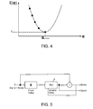
- a search algorithm can be used to descend a performance curve and find the optimum delay value. It will be useful to define a new function E( ⁇ ) proportional to the jitter transfer function T( ⁇ ) such that: E ( ⁇ ) ⁇ T ( ⁇ ) (16) where E( ⁇ ) canrepresent any function that has a one-to-one and monotonic mapping to T( ⁇ ). Examples include bit error rate and edge jitter at the decision device.
- the task of the search algorithm is to converge to a minimum value of E( ⁇ ). Since the performance curve (see the curve shown in FIG.
- FIG. 4 depicts one possible traversal of the performance curve in search of the optimum delay tuple, ( ⁇ OPTIMUM , E OPTIMUM ).
- the search described above can be performed periodically.
- the periodic interval to perform this search would be chosen based on system tolerances and dynamics. For example, the thermal time constant of the system and the temperature sensitivity of the various delay paths result in drift in the optimum value.
- the periodic interval would be chosen to keep this drift within the system operating budget.
- the search can be performed during lulls in the bus activity. Under this algorithm, there is no closed loop tracking. It may be termed an open loop periodic retrain scheme. Note that FIG. 4 represents and idealized situation. Actual curves may have multiple local minima and maxima.
- an alternative algorithm replaces and complements the search algorithm just described.
- This alternative algorithm can be used for closed loop tracking, after an optimum value is found under the previously-described algorithm, or it can be used to achieve both convergence and tracking simultaneously.
- the algorithm is presented in the discrete time domain. A continuous time version also applies and can be implemented.
- FIG. 5 shows a further simplified representation of the system model presented in FIG. 2 . The same assumptions used to derive Equation (14) are made in this simplified diagram.
- the fixed delay component between the data path and the clock path is represented by ⁇ in FIG. 5
- the variable delay component is represented by the filter transfer function H(z).
- H(z) was assumed to be a variable delay element that introduces further delay between the clock and data paths.
- H(z) will be a more generalized filter structure with filter coefficient ⁇ .
- LMS least mean square
- ⁇ ⁇ [ n ] ⁇ y ⁇ ( n ) ⁇ ⁇ ( 19 )
- Other simplified variants of this LMS algorithm can be used, such as the sign-data LMS, sign-error LMS, and sign-sign LMS.
- other training and tracking/adaptation algorithms can be used. These other alternative algorithms should include traps for outlier conditions to account for limitations in the system parameters such as a finite delay tuning range, and limitation of the physical implementation of any filter structure.
Landscapes
- Engineering & Computer Science (AREA)
- Theoretical Computer Science (AREA)
- Physics & Mathematics (AREA)
- General Engineering & Computer Science (AREA)
- General Physics & Mathematics (AREA)
- Dram (AREA)
Abstract
Description
-
- 1. The system illustrated in the
FIG. 2 block diagram uses source synchronous clocking for data transfer to the memory device. Noise analysis can start from the common source between the clock and the data path at node x1. All noise sources and contribution before node x1 are assumed to be common and correlated between the clock and the data paths; - 2. Noise margin at the sampling device is the difference (given by a difference function to be defined below) between the data path and clock path phase noise processes. Static phase de-skewing will be assumed to have taken place at time t=0 such that the noise analysis described herein is initiated at time t≧0;
- 3. The DRAM data pin insertion delay is negligible such that ΔTd1=0;
- 4. The DRAM clock pin insertion delay is dominant such that ΔTc1>>ΔTd1 and ΔTc1=ΔTDRAM;
- 5. The
PHY layer 65 clock tree is designed and constructed such that ΔTd0=ΔTd0=ΔTphy; - 6. The
PLL 240 of thememory device 20 is bypassed. The system modeling will use the x8 node in the system model block diagram ofFIG. 2 ; and - 7. System noise budget is not crosstalk dominated such that:
N xtlk-data(f)≅0∀fε[0,∞] (1)
and
N xtlk-clock(f)≅0∀fε[0,∞] (2)
Therefore, crosstalk may be neglected. Under these assumptions, the phase noise at node x1 associated with thedata channel 25 is given by:
X data(f)=X 1 ×e −2πfΔTPHY (3)
and the phase noise at node x1 associated with theclock channel 30 is given by:
X clock(f)=X 1 ×e −i2πfΔTDRAM ×e −i2πfΔTPHY (4)
The difference function S(f) for Equations (3) and (4) is given by:
S(f)=X data(f)−X clock(f)=X 1 ×e −2πfΔTPHY ×[1−e −i2πfΔTDRAM ] (5)
The magnitude of the difference function S(f) is given by:
|S(f)|2 =S(f)×S x(f)=T(f) (6)
where S*(f) denotes the conjugate function of S(f). Substituting, T(f) is given by:
T(f)=|X 1|2×[1−e −i2πfΔTDRAM ]×[1−e i2πfΔTDRAM ] (7)
Equation (7) can be further simplified by defining a variable φ as:
φf×ΔT DRAM (8)
then normalizing by:
2|X 1|2
and using trigonometric identities to convert T(f) to:
T(φ)=1−cos(2πφ) (9)
Equation (9) shows that the noise margin of the memory system at the sampling/decision device 270 (in the memory device 20) exhibits spectral nulls and peaks as a function of φ. The timing skew between the clock and the data paths leads to periodic nulls and peaks of the transmit noise X1 as shown inFIG. 3 . If:
φ=n (10)
where n is a positive integer, then T(φ)=0, i.e., a spectral null for noise transfer results, the phase noise between clock and data are correlated, and there is noise cancellation and maximum noise margin at the sampling device. However, if:
- 1. The system illustrated in the
where n is a positive integer, then T(φ)=2, i.e, a spectral peak for noise transfer results where the data and clock noise components have opposite phases, which gives minimum noise margin at the noise sampling device. The noise is doubled.
Equation (12) expresses the DRAM clock tree delay, ΔTDRAM, as a multiple a of the symbol duration or unit interval given by:
For example, a bit rate of 1.0 GB/s yields a symbol duration or unit interval of 10−9 seconds. Reexpressing T(φ) as a function of frequency leads to the following:
X 1(f)=0∀f≠1GHz (15)
E(α)∝T(α) (16)
where E(α) canrepresent any function that has a one-to-one and monotonic mapping to T(α). Examples include bit error rate and edge jitter at the decision device. The task of the search algorithm is to converge to a minimum value of E(α). Since the performance curve (see the curve shown in
e(n)=X 1(n)−y(n) (17)
Using this error signal e(n), the jitter transfer optimization can be performed with the following steepest descent algorithm:
-
- 1. Change the coefficient in the filter H(z) in and check whether the power of the error signal increased or decreased.
- 2. If it decreased, go on to the next coefficient value.
- 3. If it increased, switch the sign of the coefficient change and go on to the next coefficient value.
- 4. Repeat this procedure until the error signal e(n) is minimized.
α[n+1]=α[n]+2×μ×e[n]×Φ[n] *18)
Where μ is the tracking/adaptation parameter. It can be a constant or time variant. Φ[n] is a gradient signal of the parameter α, i.e.:
The algorithm can be initiated with α[0]=αOPTIMUM if available or an arbitrary value if the optimum value is not. Other simplified variants of this LMS algorithm can be used, such as the sign-data LMS, sign-error LMS, and sign-sign LMS. In addition to these exemplary algorithms, other training and tracking/adaptation algorithms can be used. These other alternative algorithms should include traps for outlier conditions to account for limitations in the system parameters such as a finite delay tuning range, and limitation of the physical implementation of any filter structure.
Claims (35)
Priority Applications (1)
| Application Number | Priority Date | Filing Date | Title |
|---|---|---|---|
| US13/682,487 US9223541B2 (en) | 2012-11-20 | 2012-11-20 | Method and apparatus to eliminate frequency holes in a memory I/O system |
Applications Claiming Priority (1)
| Application Number | Priority Date | Filing Date | Title |
|---|---|---|---|
| US13/682,487 US9223541B2 (en) | 2012-11-20 | 2012-11-20 | Method and apparatus to eliminate frequency holes in a memory I/O system |
Publications (2)
| Publication Number | Publication Date |
|---|---|
| US20140143585A1 US20140143585A1 (en) | 2014-05-22 |
| US9223541B2 true US9223541B2 (en) | 2015-12-29 |
Family
ID=50729119
Family Applications (1)
| Application Number | Title | Priority Date | Filing Date |
|---|---|---|---|
| US13/682,487 Active 2033-12-26 US9223541B2 (en) | 2012-11-20 | 2012-11-20 | Method and apparatus to eliminate frequency holes in a memory I/O system |
Country Status (1)
| Country | Link |
|---|---|
| US (1) | US9223541B2 (en) |
Cited By (4)
| Publication number | Priority date | Publication date | Assignee | Title |
|---|---|---|---|---|
| US10510721B2 (en) | 2017-08-11 | 2019-12-17 | Advanced Micro Devices, Inc. | Molded chip combination |
| US10593628B2 (en) | 2018-04-24 | 2020-03-17 | Advanced Micro Devices, Inc. | Molded die last chip combination |
| US10923430B2 (en) | 2019-06-30 | 2021-02-16 | Advanced Micro Devices, Inc. | High density cross link die with polymer routing layer |
| US11833826B2 (en) | 2018-06-04 | 2023-12-05 | Mevam Bv | Add-on module for a disposable printer cartridge and a printer |
Families Citing this family (2)
| Publication number | Priority date | Publication date | Assignee | Title |
|---|---|---|---|---|
| US11310075B2 (en) * | 2014-04-02 | 2022-04-19 | Aten International Co., Ltd. | Asymmetric duplex transmission device and switching system thereof |
| US20160132072A1 (en) * | 2014-11-10 | 2016-05-12 | Intel Corporation | Link layer signal synchronization |
Citations (5)
| Publication number | Priority date | Publication date | Assignee | Title |
|---|---|---|---|---|
| US20070036256A1 (en) * | 2001-03-20 | 2007-02-15 | Advantest Corporation | Apparatus for and method of measuring clock skew |
| US20070217559A1 (en) * | 2006-03-16 | 2007-09-20 | Rambus Inc. | Signaling system with adaptive timing calibration |
| US20080301485A1 (en) * | 2007-05-30 | 2008-12-04 | Texas Instruments Deutschland Gmbh | Register with process, supply voltage and temperature variation independent propagation delay path |
| US20110025389A1 (en) * | 2009-04-01 | 2011-02-03 | Yantao Ma | Clock jitter compensated clock circuits and methods for generating jitter compensated clock signals |
| US20110249718A1 (en) * | 2008-12-31 | 2011-10-13 | Rambus Inc. | Method and apparatus for correcting phase errors during transient events in high-speed signaling systems |
-
2012
- 2012-11-20 US US13/682,487 patent/US9223541B2/en active Active
Patent Citations (5)
| Publication number | Priority date | Publication date | Assignee | Title |
|---|---|---|---|---|
| US20070036256A1 (en) * | 2001-03-20 | 2007-02-15 | Advantest Corporation | Apparatus for and method of measuring clock skew |
| US20070217559A1 (en) * | 2006-03-16 | 2007-09-20 | Rambus Inc. | Signaling system with adaptive timing calibration |
| US20080301485A1 (en) * | 2007-05-30 | 2008-12-04 | Texas Instruments Deutschland Gmbh | Register with process, supply voltage and temperature variation independent propagation delay path |
| US20110249718A1 (en) * | 2008-12-31 | 2011-10-13 | Rambus Inc. | Method and apparatus for correcting phase errors during transient events in high-speed signaling systems |
| US20110025389A1 (en) * | 2009-04-01 | 2011-02-03 | Yantao Ma | Clock jitter compensated clock circuits and methods for generating jitter compensated clock signals |
Non-Patent Citations (2)
| Title |
|---|
| Wikipedia; Jitter; http://en.wikipedia.org/wiki/Jitter; May 21, 2012; pp. 1-7. |
| Wikipedia; Phase Noise; http://en.wikipedia.org/wiki/Phase-noise; Jun. 14, 2012; pp. 1-4. |
Cited By (5)
| Publication number | Priority date | Publication date | Assignee | Title |
|---|---|---|---|---|
| US10510721B2 (en) | 2017-08-11 | 2019-12-17 | Advanced Micro Devices, Inc. | Molded chip combination |
| US10593628B2 (en) | 2018-04-24 | 2020-03-17 | Advanced Micro Devices, Inc. | Molded die last chip combination |
| US11211332B2 (en) | 2018-04-24 | 2021-12-28 | Advanced Micro Devices, Inc. | Molded die last chip combination |
| US11833826B2 (en) | 2018-06-04 | 2023-12-05 | Mevam Bv | Add-on module for a disposable printer cartridge and a printer |
| US10923430B2 (en) | 2019-06-30 | 2021-02-16 | Advanced Micro Devices, Inc. | High density cross link die with polymer routing layer |
Also Published As
| Publication number | Publication date |
|---|---|
| US20140143585A1 (en) | 2014-05-22 |
Similar Documents
| Publication | Publication Date | Title |
|---|---|---|
| US9223541B2 (en) | Method and apparatus to eliminate frequency holes in a memory I/O system | |
| Sonntag et al. | A digital clock and data recovery architecture for multi-gigabit/s binary links | |
| Sidiropoulos et al. | A semidigital dual delay-locked loop | |
| EP1394949B1 (en) | Clock generator for generating an accurate and low-jitter clock | |
| Ye et al. | A multiple-crystal interface PLL with VCO realignment to reduce phase noise | |
| US5870594A (en) | Data transfer system and method | |
| US7844023B2 (en) | Phase offset cancellation for multi-phase clocks | |
| TWI484318B (en) | Clock data recovery circuit module and method for generating data recovery clock | |
| KR102240293B1 (en) | System and method for maintaining high speed communication | |
| JP4542286B2 (en) | Parallel signal automatic phase adjustment circuit | |
| KR101172270B1 (en) | Duty-cycle correction in a delay-locked loop | |
| KR20140010667A (en) | Semiconductor device and method of driving the same | |
| KR100849222B1 (en) | Method and Record readable medium, and apparatus for controlling transmission frequency in Serial Advanced Technology Attachment | |
| Agrawal et al. | An 8$\,\times\, $5 Gb/s Parallel Receiver With Collaborative Timing Recovery | |
| Lee et al. | A 0.8-to-6.5 Gb/s continuous-rate reference-less digital CDR with half-rate common-mode clock-embedded signaling | |
| US8782458B2 (en) | System and method of data communications between electronic devices | |
| KR101610625B1 (en) | Authentication system and method for device using physically unclonable function | |
| Casper | Clocking wireline systems: An overview of wireline design techniques | |
| US7555089B2 (en) | Data edge-to-clock edge phase detector for high speed circuits | |
| Ragab et al. | Receiver Jitter Tracking Characteristics in High‐Speed Source Synchronous Links | |
| KR100892637B1 (en) | Clock Distribution Circuit and Interface Device Using the Same | |
| US8742809B2 (en) | Delay-locked loop having a loop bandwidth dependency on phase error | |
| KR101212735B1 (en) | Delay-locked loop having loop bandwidth dependency on operating frequency | |
| US9049020B2 (en) | Circuitry to facilitate testing of serial interfaces | |
| Wahid | Hybrid Pulse-Amplitude-Modulation Signaling Scheme and Clock Synthesis for Next Generation Ultra-High-Speed Wire-Line Receivers |
Legal Events
| Date | Code | Title | Description |
|---|---|---|---|
| AS | Assignment |
Owner name: ADVANCED MICRO DEVICES, INC., CALIFORNIA Free format text: ASSIGNMENT OF ASSIGNORS INTEREST;ASSIGNOR:BARAKAT, SHADI;REEL/FRAME:029332/0984 Effective date: 20121114 |
|
| STCF | Information on status: patent grant |
Free format text: PATENTED CASE |
|
| MAFP | Maintenance fee payment |
Free format text: PAYMENT OF MAINTENANCE FEE, 4TH YEAR, LARGE ENTITY (ORIGINAL EVENT CODE: M1551); ENTITY STATUS OF PATENT OWNER: LARGE ENTITY Year of fee payment: 4 |
|
| MAFP | Maintenance fee payment |
Free format text: PAYMENT OF MAINTENANCE FEE, 8TH YEAR, LARGE ENTITY (ORIGINAL EVENT CODE: M1552); ENTITY STATUS OF PATENT OWNER: LARGE ENTITY Year of fee payment: 8 |